coulomb blockade and single-electron transistors eee5425 introduction to nanotechnology1
TRANSCRIPT

EEE5425 Introduction to Nanotechnology 1
COULOMB BLOCKADE AND SINGLE-ELECTRON TRANSISTORS

© Nezih Pala [email protected] EEE5425 Introduction to Nanotechnology 2
Nanocapacitor
With the basics of tunneling described in earlier, we can examine the “connection” between a quantum dot and electrical leads depicted in the figure. It turns out that tunneling is the process by which current can flow from lead to lead through quantum dot. In this type of situation, the quantum dot, which is merely a very small material region, is also called a quantum island or Coulomb island. We will model the quantum dot and the exterior leads using the classical concept of capacitance and consider electron conduction via tunneling and so we use a mixed classical-quantum model. As we will see, one of the most fundamental effects in nanoelectronics is related to the significant change in energy when a single electron is transferred into a nanoscopic material region, such as quantum dot leading to what is known as Coulomb Blockade.
Lead LeadQuantum dot

© Nezih Pala [email protected] EEE5425 Introduction to Nanotechnology 3
Nanocapacitor
Early studies of Coulomb blockade arose out of the consideration of electron transport through materials consisting of granular metallic particles. It was realized that current flow through the material could be inhibited if the capacitance of the particle was sufficiently small. However, only more recently has the phenomenon been extensively studied using modern experimental methods. In the following, we first consider a generic tunnel junction consisting of two conductors separated by an insulating gap, after which we examine more complicated structures, leading up to the study of a single-electron transistor. Recall that for two conductors separated by an insulator, charge and voltage are proportional.
where Q is the charge on the conductors (+Q on one conductor and -Q on the other), C is the capacitance, and V is the d.c. voltage between the conductors. The electrostatic energy stored in a capacitor is
which is the energy required to separate the charges initially upon applying the potential across the conductors (i.e., the work that must be done by a source to establish the charge configuration on the capacitor surfaces).
VCQ
C
QCVE
22
1 22

© Nezih Pala [email protected] EEE5425 Introduction to Nanotechnology 4
NanocapacitorThe simplest capacitor is formed by two parallel plates of area A and plate separation d. For this configuration,
A (nm2 ) d (nm) C (F) ∆E (eV)
Nanocapacitor 52 2 1.1 x10⁻¹⁹ 0.73
Nanocapacitor 802 1 5.7 x 10⁻¹⁷ 0.0014
μ capacitor (5 x 10³ )2 2 1.1 x 10⁻¹³ 7.3 X 10⁻⁷
mm capacitor (5 x 10⁶ )2 2x10⁶ 1.1 x10⁻¹³ 7.3 X 10⁻⁷
As can be seen, the nanoscale capacitors have extremely small values of capacitance.
For nanoscale dimensions, the small values of capacitance lead to the interesting observation that the transfer of a single electron results in an appreciable energy change. For example, for the nanoscale capacitor having C = 1.1 x 10⁻¹⁹ F, the transfer of a single electron yields a change in energy ∆E that is an appreciable fraction of an electron volt. For the macroscopic capacitor (C = 1.1 x10⁻¹³ F), the change in energy due to the transfer of a single electron is negligible. For nanoscale capacitors, it is this sensitivity to the transfer of an extremely small amount of charge that allows for the possibility of so-called single-electron precision devices.

© Nezih Pala [email protected] EEE5425 Introduction to Nanotechnology 5
Coulomb Blockade in a Nanocapacitor -1Consider a small capacitor made by creating an insulating layer between two metal surfaces, and assume that the capacitor plates carry charges ±Q. The initial energy stored in the electrostatic field between the capacitor plates is given
Note that even though charge itself is quantized (in units of |qe|), the charge Q on the capacitor plates is not quantized. The charge on the capacitor plates (sometimes called a polarization charge) merely represents a displacement of electrons relative to a background of positive ions. That is, certain electrons may be found nearer to, or farther from, the material's surface, depending on the situation. These discrete charges can, in this way, contribute a continuous amount of charge to the interface. Therefore, the discreteness of electronic charge does not show up in macroscopic circuits for two reasons. First, because there are so many electrons involved (for example, 1 mA d.c. current corresponds to the movement of 6.25 x 10¹⁵ electrons/second, since A = C/s), and second, because discrete charges can contribute continuous amounts of charge to an interface.
C
QE i
2
2
+Q
-QV

© Nezih Pala [email protected] EEE5425 Introduction to Nanotechnology 6
Coulomb Blockade in a Nanocapacitor -2
Now let a single electron tunnel through the insulating layer from the negative terminal to the positive terminal, such that charge Q + qe resides on the top plate, and -Q - qe . resides on the bottom plate. The energy stored in the field of the capacitor is now
C
qQE ef
2
2
such that the change in energy stored is C
qQqEEE eeif
22/)(
It must be energetically favorable for the tunneling event to occur, and if we require ΔE < 0, remembering that qe<0 we find that
2eqQ
for tunneling to occur.
andC
qV e
2
Repeating for the opposite polarity, we find that in order for tunneling to occur, we must have
C
qV
C
q ee
22
That is, tunneling current will only flow when a sufficiently large voltage ( |V|> |qe|/2C) exists across the capacitor. This effect is called Coulomb blockade.

© Nezih Pala [email protected] EEE5425 Introduction to Nanotechnology 7
Coulomb Blockade in a Nanocapacitor -3
V
I
|qe|/2C
Since qeV is energy
is called the charging energy of the capacitor. This is the energy required to add a charge to the capacitor, which is, itself, a classical idea based on charge repulsion. The resulting I -V characteristics depicting Coulomb blockade are shown in the figure.
C
qE ec 2
2
For example, in the small yet macroscopic capacitor, where C = 1.1 x 10⁻¹³ F, we only need IV I > 0.73 μV for tunneling to occur. Note, however, that regardless of the voltage, capacitor plate separation d must be adequately small such that tunneling can take place.
For the nanoscale capacitor with C = 5.7 x 10⁻¹⁷ F we need IVI > 1.4 mV to have tunneling, and for the nanoscale capacitor with C = 1.1 x 10⁻¹⁹ F, lV|> 0.73 V is required. Thus, Coulomb blockade is not evident in macro-sized circuits because the charging energy is so low, but may be observed in nanometer scale circuits.

© Nezih Pala [email protected] EEE5425 Introduction to Nanotechnology 8
Coulomb Blockade in a Nanocapacitor -4
Temperature plays an important role in Coulomb blockade phenomena. The preceding development is only strictly valid at T = 0 K. For higher temperatures, thermal energy is available such that the condition E > 0 (where E is based on (7.2) can be relaxed. We typically need the charging energy to be greater than the thermal energy,
to observe Coulomb blockade, where kB is Boltzmann's constant. Put simply, if the last equation is not satisfied there is too much thermal energy available to the electron to be held back by the charging energy Ec of the capacitor. For the nanoscale capacitor considered previously (C = 1.1 x 10⁻¹⁹ F), T << 16,911 K, which is obviously the typical situation. Therefore, we should be able to observe Coulomb blockade for this capacitor at any practical temperature. However, for the macroscale capacitor (C = 1.1 x 10⁻¹³ F), T <<0.017 K, which is difficult to achieve. (This, of course, explains why Coulomb blockade is not seen in macroscale electronics at room temperature.) For the somewhat larger nano-scale capacitor (C = 5.7 X 10⁻¹⁷ F), T <<32.6 K.
TkC
qB
e
2
1
2
2
Tk
qC
B
e2
or

© Nezih Pala [email protected] EEE5425 Introduction to Nanotechnology 9
Coulomb Blockade in a Nanocapacitor -5
We can also gain an appreciation of the effect of thermal fluctuations by considering the following argument. If, rather than having a single-electron tunnel, we assume that n electrons tunnel as a group, i.e., that a charge of nqe is the tunneling object, it is easily shown that
replace the expressions derived previously for the single charge case. Equating the charging energy to the thermal energy, we have
which is, roughly, the number of electrons (or the uncertainty in the number of electrons) that could be transferred due to thermal energy. Assuming room temperature operation (T = 293 K), if C = 1 fF then n = 13 electrons can be transferred by thermal energy. However, if C = 7 aF, then n = 1. It is obvious that as C and/or T decrease, the uncertainty in the number of electrons transferred can be reduced to an acceptable value, at which point Coulomb blockade can be observed.
C
nqV
C
nq ee
22
C
nqE ec 2
2
2e
B
q
TCkn

© Nezih Pala [email protected] EEE5425 Introduction to Nanotechnology 10
Tunnel Junctions -1The tunneling that occurs across the capacitor can be accounted for by considering the capacitor to be a leaky capacitor, modeled by an ideal capacitance in parallel with a resistance Rt = V /I, where V is a d.c. voltage applied across the junction and I is the resulting current due to tunneling.
This tunneling resistance is not an ordinary resistance, but conceptually allows electrons to cross the insulating junction as discrete events. The parallel combination of the capacitor and the tunneling resistance is called a tunnel junction, and is depicted in the figure.
The tunneling effect accounted for by Rt should be weak enough (i.e., Rt should be sufficiently large) to prevent the charge of the tunneling electrons from becoming delocalized over (i.e., shared by) the capacitor plates. However, Rt must be finite, and not too large, so that tunneling can actually take place. In this case, the charge on the island is said to be "well quantized," and the leaky capacitor is considered to be a tunnel junction. Considering the discussion of tunneling earlier, we can appreciate that Rt is related to the potential energy barrier width, i.e., the separation between the capacitor plates.

© Nezih Pala [email protected] EEE5425 Introduction to Nanotechnology 11
Tunnel Junctions -2
SEM images of tunnel junction devices made with 2D arrays of Au islands. (a) The Au islands cover the whole surface, and the width of the array is roughly given by the width of the source and drain electrodes (here, 80 nm; the interelectrode gap is 20 nm), (b) A patterned array where the islands are only kept under a narrow resist line between the contact electrodes. From Pepin, A., et a1., "Temperature Evolution of Multiple Tunnel Junction Devices Mode with Disordered Two-Dimensional Arrays of Metallic Islands," Appl. Phys. Lett. 74 (1999): 3047.

© Nezih Pala [email protected] EEE5425 Introduction to Nanotechnology 12
Tunnel Junctions -3
Typical 1-V characteristics of the devices shown in the previous pictures, where an 8 x 5 array of Au islands occur in the interelectrode gap. (Curves have been offset for clarity.)

© Nezih Pala [email protected] EEE5425 Introduction to Nanotechnology 13
Tunnel Junctions -2
In order to see Coulomb blockade, we need to limit tunneling to some degree, and we can get an estimate of this by considering the uncertainty relation between time and energy
Given that the time constant of a parallel RC circuit is
2/ tE
RC
then τ = RtC is a characteristic time associated with tunneling events. This is not the time to tunnel through the junction, but, rather, the time between tunneling events; τ is considered to be the approximate lifetime of the energy state of the electron on one side of the barrier. Thus, considering the uncertainty in energy
C
qE e
2
2
we obtain22
22 CR
C
qtE t
e
To observe the Coulomb blockade effect, the charging energy must be much larger than this uncertainty, such that
kq
Re
t 1.42

© Nezih Pala [email protected] EEE5425 Introduction to Nanotechnology 14
Tunnel Junction Excited by a Current Source -1An interesting circuit that leads to a surprisingly complex phenomenon consists of a tunnel junction fed by a constant current source IS as depicted in the figure.
For a classical ideal capacitor (no tunneling allowed), the relation between voltage and current,
dt
dVCI
leads to the conclusion that the voltage over a current-source-driven capacitor will increase linearly with respect to time,
tC
IdtI
CtV S
t
S 0
1)( tItQ S)(as will the charge
Even though no d.c. current can pass through the capacitor, one has the idea that the current source is pushing electrons onto the capacitor plate, where they are stored, building up the voltage and accumulated charge. For a real capacitor that admits tunneling, at the point when
2eqQ and
C
qV e
2

© Nezih Pala [email protected] EEE5425 Introduction to Nanotechnology 15
Tunnel Junction Excited by a Current Source -2
For a real capacitor that admits tunneling, at the point when
2eqQ and equivalently
C
qV e
2
tunneling from the lower to the upper capacitor plate can occur (since Coulomb blockade is then thwarted). This results in a decrease in the positive charge on the top plate,
and an increase in the positive charge on the bottom plate,
The voltage then decreases by |qe|/C , and the process repeats itself, as shown in the figure . The net result is that the voltage across the capacitor oscillates, which is known as single-electron tunneling (SET) oscillations.
|| ee qQqQQ
|| ee qQqQQ

© Nezih Pala [email protected] EEE5425 Introduction to Nanotechnology 16
Tunnel Junction Excited by a Current Source -3The period of oscillation can be calculated as
S
ST
S I
eT
C
eT
C
IdtI
CTtV 22
1)2/(
2/
0
Therefore, the time between tunneling events is on the order of 10-10 s assuming nanoamp currents (i.e., |qe|/10-9 = 1.6 x 10⁻¹⁰), which is much larger than the typical tunneling time of 10-14 s.
It turns out that the previously described oscillation is difficult to observe due to experimental factors, such as the generally high lead capacitance in experimental systems. To assess this issue, consider the world as seen by the tunnel junction. In a circuit model, the tunnel junction is connected to external bias and measurement circuitry by some lengths of electrical leads. The fact that there is no direct electrical contact between the island and the leads is modeled by the tunnel junction itself, via the tunnel resistance Rt and junction capacitance C.

© Nezih Pala [email protected] EEE5425 Introduction to Nanotechnology 17
Coulomb Blockade in a Quantum Dot Circuit -1
We are now in a position to consider a metallic quantum dot coupled to external leads, as shown in the figure with the equivalent circuit where, to a first approximation, we can ignore the external environment. This is a valid approximation due to the presence of two tunnel junctions (and, hence, of an isolated charge island).
The tunnel junctions represent the insulating regions isolating the island (dot) from the leads connected to an external source V,. The tunnel junctions can be modeled by leaky capacitors, i.e., a capacitance in parallel with a resistance. Therefore, for one junction, we have Ca , and Rta , and for the other junction, Cb and Rtb . where Rti is the tunneling resistance of junction i. Associated with each tunnel junction, we have
bbbaaa VCQVCQ ,
ab QQQ such that the net charge on the island is the difference

© Nezih Pala [email protected] EEE5425 Introduction to Nanotechnology 18
Coulomb Blockade in a Quantum Dot Circuit -2Electron tunneling allows a discrete number of electrons to accumulate on the island, and so
enqQ where n is an integer. Note that in this semiclassical model, the discrete index n and the continuous charge Q are classical (not quantum) quantities, with well-defined values at all times. The energy stored in the capacitors is
2222
2
1
22 bbaab
b
a
ase VCVC
C
Q
C
QE
Kirchhoff's voltage law applied to the circuit yields
b
aaa
b
aa
b
babas C
VCQV
C
QQV
C
QVVVV
)()(
leading to, using Q = nqe
ebss
a nqCVC
V 1 eas
sb nqCVC
V 1
and
where Cs = Ca + Cb.
© Nezih Pala [email protected] EEE5425 Introduction to Nanotechnology 19
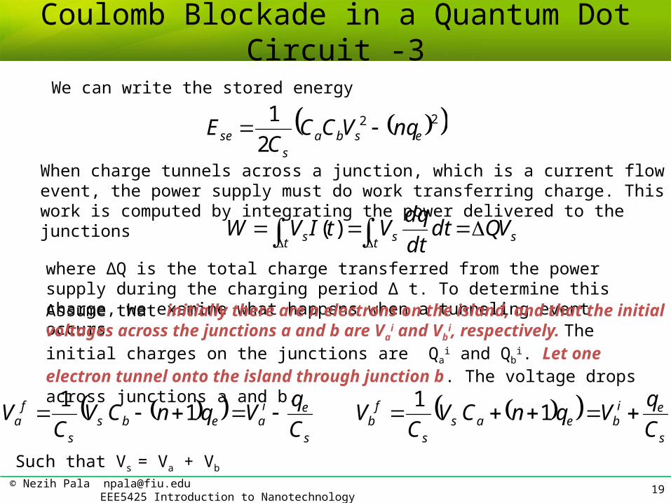
Coulomb Blockade in a Quantum Dot Circuit -3
We can write the stored energy
22
2
1esba
sse nqVCC
CE
When charge tunnels across a junction, which is a current flow event, the power supply must do work transferring charge. This work is computed by integrating the power delivered to the junctions
where ∆Q is the total charge transferred from the power supply during the charging period ∆ t. To determine this charge, we examine what happens when a tunneling event occurs.
st st s VQdtdt
dqVtIVW
)(
Assume that initially there are n electrons on the island, and that the initial voltages across the junctions a and b are Va
i and Vbi, respectively. The initial charges on the
junctions are Qai and Qb
i. Let one electron tunnel onto the island through junction b. The voltage drops across junctions a and b.
s
eiaebs
s
fa C
qVqnCV
CV 1
1 s
eibeas
s
fb C
qVqnCV
CV 1
1
Such that Vs = Va + Vb

© Nezih Pala [email protected] EEE5425 Introduction to Nanotechnology 20
Coulomb Blockade in a Quantum Dot Circuit -4The resulting charge stored by junction a is
s
eaia
s
eaiaa
faa
fa C
qCQ
C
qCVCVCQ
The change in charge ΔQa = Qaf - Qa
i must come from the power supply (the change in charge on junction b is associated with the tunneling event), and is associated with the supply doing work
s
eas C
qCVW
Upon the electron tunneling onto the island through junction b, the change in the total energy (the change in the stored energy minus the work done ) is
s
easesba
sesba
s
set
C
qCVqnVCC
CnqVCC
C
WEE
2222 ))1((2
1)(
2
1
This energy change must be positive for the tunneling event to b energetically favorable.

© Nezih Pala [email protected] EEE5425 Introduction to Nanotechnology 21
Coulomb Blockade in a Quantum Dot Circuit -5
Therefore
0)2
1(
ase
s
e CVnqC
q)
2
1( n
C
qV
a
essuch that
In a similar manner, when an electron tunnels off the island through junction a, the voltage across the junction change as
s
eiaebs
s
fa C
qVqnCV
CV 1
1 s
eibeas
s
fb C
qVqnCV
CV 1
1
And the resulting charge stored in junction b is
s
ebib
s
ebibbbb
fb C
qCQ
C
qCVCVCQ
Associated with work
s
ebs C
qCVW

© Nezih Pala [email protected] EEE5425 Introduction to Nanotechnology 22
Coulomb Blockade in a Quantum Dot Circuit -6
The change in the total energy is
s
ebsesba
sesba
s
set
C
qCVqnVCC
CnqVCC
C
WEE
2222 ))1((2
1)(
2
1
Requiring this to be positive (the system must evolve from higher energy to a lower energy stat, in the absence of any other energy input ) we have
0)2
1(
bse
s
e CVnqC
q)
2
1( n
C
qV
b
esleading to
As a special case, if we let Ca=Cb=C and n=0 then Vs for both previous cases reduce to
C
qV es 2

© Nezih Pala [email protected] EEE5425 Introduction to Nanotechnology 23
Coulomb Blockade in a Quantum Dot Circuit -7
Now consider the opposite situation, where an electron tunnels onto the island through junction and off the island through junction b. For Ca=Cb=C and n=0 we would find
C
qV es 2
Thus under these conditions, we have
C
qV
C
q es
e
22
C
eVs 2
or
The same Coulomb blockade as encountered for a single capacitor and associated charging energy Ec = qe
2/2C

© Nezih Pala [email protected] EEE5425 Introduction to Nanotechnology 24
Coulomb Blockade in a Quantum Dot Circuit -8
Consider a junction with identical capacitances, (Ca = Cb = C), and one where the island is very large. In this case, the charge on the island is not well discretized, and the Fermi energy on the island is approximately that of the bulk material. Assuming that the island and leads are made of the same material, at are at thermal equilibrium, we find that the energy band diagram is as shown in the upper figure.
If a potential difference V0 is applied across the structure, the energy levels will shift as shown in the lower figure, allowing tunneling to occur onto or off of the island.

© Nezih Pala [email protected] EEE5425 Introduction to Nanotechnology 25
Coulomb Blockade in a Quantum Dot Circuit -9
Now let the island be very small, such that the energy levels are well discretized and the charging energy is significant compared to the Fermi level. In this case, for which the previous development applies, the charging energy is represented by an energy gap (a range of energies for which there are no states) of size e2/2C, which appears symmetrically about the Fermi level if the junctions are symmetric. as shown in the upper figure. On the island, empty states appear above the gap.
If a voltage is applied across the structure, then the band diagram. If the applied voltage is slightly larger than e2/2C, the. the band diagram becomes as shown the lower figure allowing an electron to tunnel onto the island.

© Nezih Pala [email protected] EEE5425 Introduction to Nanotechnology 26
Coulomb Blockade in a Quantum Dot Circuit -10
After the electron tunnels onto the island. the energy on the island i increased by e2/2C. readjusting the energy bands, and Coulomb blockade is re-established until either |V|>3e/2C (as explained later) or the electron tunnels off of the island, reducing the island's energy by e2/2C. Now assume that one electron has already tunneled onto the island through junction b. If a second electron tunnels onto the dot through junction b, the change in energy is
s
easesba
sesba
s
set
C
qCVqnVCC
CqnVCC
C
WEE
2222 ))2((2
1))1((
2
1
and enforcing ∆Et > 0 leads to
0)2
3(
ase
s
e CVnqC
qsuch that
C
qV es 2
||3

© Nezih Pala [email protected] EEE5425 Introduction to Nanotechnology 27
Coulomb Blockade in a Quantum Dot Circuit -11
Considering a third tunneling event, we would obtain
C
qV es 2
||5
and, in general, we have
C
meVs 2
m = 1,3,5, ... , for 1,2,3, ... electron tunneling events, respectively. Thus, electron tunneling events, giving rise to currents, will occur at discrete voltage steps. The resulting I-V characteristic, known as a Coulomb staircase, is depicted in the figure, where V1= e/(2C), and I1 = e/(RtCs) .

© Nezih Pala [email protected] EEE5425 Introduction to Nanotechnology 28
Coulomb Blockade in a Quantum Dot Circuit -12We usually need to have asymmetric junctions to observe the Coulomb staircase, and it is often convenient to have Ca = Cb = C, but Rta >> Rtb , or Rta << Rtb . This can be achieved by having different-sized insulating gaps separating the leads from the island. In this way, the junctions have different tunneling rates. For example, assume that Rta >> Rtb . Then, tunneling is limited by junction a, so that as soon as one electron tunnels off of the island through junction a, it will be quickly replaced by a tunneling event through junction b. In this case, since junction a approximately controls tunneling, the resulting current will be ∆I ~ ∆Va/ Rta .Hence
s
eia
faa C
qVVV
sta
e
ta
aa CR
q
R
VI
and so the resulting current is
as shown in the last figure (In the figure, I is normalized by I1 = Iqe|/ (RtCs), where Rt, is the larger of the tunnel resistances.)

© Nezih Pala [email protected] EEE5425 Introduction to Nanotechnology 29
Coulomb Blockade in a Quantum Dot Circuit -13
Experimental results showing the Coulomb staircase are shown in the figure. In this experiment, the setup consisted of an In droplet separated from an Al ground plane by a tunneling oxide layer approximately 1 nm thick. An STM tip is brought into close proximity to the droplet, forming a metal-insulator-island-insulator-metal junction, as depicted in the figure below.
From Wilkins, R., E. Ben-Jacob, and R. C. Jaklevic, "Scanning-Tunneling-Microscope Observations of Coulomb Blockade and Oxide Polarization in Small Metal Droplets," Phys. Rev. Lett. 63 (1989)

© Nezih Pala [email protected] EEE5425 Introduction to Nanotechnology 30
Single Electron Transistor -1
We can gain additional control of the double-tunnel junction by adding a gate terminal, isolated from the island by an ideal (no tunneling) gate capacitance, and connected to a gate voltage, as depicted by the circuit shown in the figure. This device is called a single-electron tunneling transistor (SET transistor), or simply a single-electron transistor (SET).

© Nezih Pala [email protected] EEE5425 Introduction to Nanotechnology 31
Single Electron Transistor -2
Jukka P. Pekola, Juha J. Vartiainen, Mikko Möttönen, Olli-Pentti Saira, Matthias Meschke & Dmitri V. Averin Nature Physics 4, 120 - 124 (2008)

© Nezih Pala [email protected] EEE5425 Introduction to Nanotechnology 32
Single Electron Transistor -3
The effect of the gate electrode can easily be understood from an energy band diagram as shown in the figure. Application of a gate voltage Vg > 0 depresses the Fermi level on the island. Depending on how much gate voltage is applied, the top of the energy gap can be made to lie above, below, or even with the left and right Fermi levels. Thus, the strength of the applied source-drain voltage Vs required to drive a current through the device can be varied at the gate.
Following a development similar to that presented in the previous discussion, we have
)(
,
bggg
bbbaaa
VVCQ
VCQVCQ
such that the net charge on the island is the difference
egab nqQQQQ

© Nezih Pala [email protected] EEE5425 Introduction to Nanotechnology 33
Single Electron Transistor -4
The energy stored in the capacitors is
g
g
b
b
a
ase C
Q
C
Q
C
QE
222
2
1
and Kirchhoff's voltage law applied to the circuit yields
b
b
g
gbggg
b
b
a
abas C
Q
C
QVVV
C
Q
C
QVVV ,
So we can obtain
s
gggbsaa C
QVCCCVCQ
)(
s
ggsabb C
QVCVCCQ
s
saabggg C
QVCCCVCQ
)()(
where Cs = Ca + Cb + Cg , and the stored energy is
2222)(2
1QVCCVCCVVCC
CE ggbsbagsag
sse

© Nezih Pala [email protected] EEE5425 Introduction to Nanotechnology 34
Single Electron Transistor -5When charge tunnels across a junction (i.e., a current flow event occurs), the power supplies must do work transferring charge. Assume that one electron tunnels onto the island through junction b. The change in stored energy is
se
s
eese C
nq
C
qnnqE
2
12
2
))1(()( 222
and the change in charge on junction a and on the gate is
The work associated with supplying this change is s
egg
s
eaa C
qCQ
C
qCQ ,
gs
eggggs
s
easaa V
C
qCVQWV
C
qCVQW ,
and, requiring that the tunneling event be energetically favorable,
0)( gaset WWEE 02
1
ggsae VCVCnqresulting

© Nezih Pala [email protected] EEE5425 Introduction to Nanotechnology 35
Single Electron Transistor -6In a similar manner, for an electron on the island to tunnel off of the island through junction a, we would find that
To consider current flow, assume that initially the island is charge neutral (n = 0), and that an electron tunnels onto the island through junction b. Then, for tunneling to occur, we need
02
1
gggbse VCCCVnq
gg
e
as VC
q
CV
2
1
which is plotted in the figure.

© Nezih Pala [email protected] EEE5425 Introduction to Nanotechnology 36
Single Electron Transistor -7
Now n = 1, and for the electron to tunnel off of the island through junction a, we need
gg
e
gbs VC
q
CCV
2
1
which is depicted in the upper figure.
For positive current to flow (l > 0; positive current flow is from top to bottom), the electron must tunnel onto the island through junction b, then off of the island through junction a, and so both conditions need to be met, resulting in the lower figure.

© Nezih Pala [email protected] EEE5425 Introduction to Nanotechnology 37
Single Electron Transistor -8
Now if we assume that there is already one electron on the island, and another electron tunnels onto the island through junction b, then off of the island through junction a, we obtain
gge
as VC
q
CV
2
31
gg
e
gbs VC
q
CCV
2
31
Continuing in this manner, and considering the opposing tunneling events (that is, an electron tunneling onto the island through junction a, and then off of the island through junction b), we obtain the Coulomb diamonds shown in the figure, where V1= e/ (2Cg). This is also called a charge stability diagram, since for combinations of Vs and Vg lying within the shaded regions, no tunneling is allowed (I = 0) and the charge on the island will remain stable.

© Nezih Pala [email protected] EEE5425 Introduction to Nanotechnology 38
Single Electron Transistor -9
For the center shaded region, n = 1, and, moving outwards from the center, each shaded region corresponds to an integral change in the charge.
Note that by adjusting the gate voltage, one can tune the effective Coulomb gap seen by Vs. For Vg = me/2Cg, m = ± I, ±3, ±5, ... , there is no Coulomb gap, and current will flow for a small voltage Vs. However, for m = 0, ±2, ±4, ±6, ... , there is a maximum Coulomb gap that must be overcome in order for current to flow.

© Nezih Pala [email protected] EEE5425 Introduction to Nanotechnology 39
Single Electron Transistor -10
The Coulomb diamond has been observed in a variety of experiments where both Vg and Vs are varied. For example, in the figure below the experimental conductance of a metal junction SET is shown, clearly exhibiting the Coulomb diamond structure.
The conductance of a SET (dI/dVg) plotted versus the bias voltage (Vs) and the gate voltage Vg The gray diamonds are regions of Coulomb blockade (zero conduction). White is positive differential conductance and black is negative differential conductance; T = 50 mK.
From Hadley, P., et al., "Single-Electron Effects in Metals and Nanotubes for Nanoscale Circuits," in Proceedings of the MIOP-The German Wireless Week. 11th Conference on Microwaves, Radio Communication and Electromagnetic Compatibility, Stuttgart, Germany, 2001. 408-412.