controlled polymer nanostructures by alternative lithography
TRANSCRIPT

CONTROLLED POLYMER NANOSTRUCTURES
by
ALTERNATIVE LITHOGRAPHY

This research has been supported by the MESA+ Institute for Nanotechnology (SRO
Nanofabrication).
Controlled Polymer Nanostructures by Alternative Lithography
Canet Acikgoz
Ph. D. Thesis
University of Twente, Enschede, The Netherlands
ISBN: 978-90-365-2976-1
Publisher: Ipskamp Drukkers B. V., Josink Maatweg 43, 7545 PS, Enschede,
The Netherlends, http://www.ipskampdrukkers.nl
© Canet Acikgoz, Enschede, 2010
Cover graphics: www.filminthefridge.com
No part of this work may be reproduced by print, photocopy or any other means without the
permission in writing of the author.

CONTROLLED POLYMER NANOSTRUCTURES BY
ALTERNATIVE LITHOGRAPHY
PROEFSCHRIFT
ter verkrijging van
de graad van doctor aan de Universiteit Twente,
op gezag van de rector magnificus,
prof. dr. H. Brinksma,
volgens besluit van het College voor Promoties
in het openbaar te verdedigen
op vrijdag 12 februari 2010 om 15.00 uur
door
Canet Acikgoz
geboren op 10 januari 1980
te Iskenderun, Turkije

Dit proefschrift is goedgekeurd door:
Promotoren: Prof. dr. ir. Jurriaan Huskens
Prof. dr. G. Julius Vancso
Assistent Promotor: Dr. Mark A. Hempenius

This thesis is dedicated to my family


Table of Contents
Chapter 1 General introduction 1
Chapter 2 Conventional and Alternative Lithography Techniques for the
Fabrication of Nanostructures
7
2.1. Introduction 8
2.2. Conventional Lithography 9
2.2.1 Photolithography 9
2.2.2 Serial Writing with Charged Particles 11
2.2.2.1 Electron Beam Lithography 11
2.2.2.2 Ion Beam Lithography 12
2.3. Alternative Lithographies 12
2.3.1 Mold Fabrication 14
2.3.2 Nanoimprint Lithography 15
2.3.3 Ultraviolet-assisted Nanoimprint Lithography 19
2.3.4 Soft Lithography
2.3.5 Colloidal Lithography
2.3.5.1 Synthetic Methods to Prepare Colloidal Particles
2.3.5.2 Methods of Colloidal Crystal Assembly
2.3.5.3 Nanopatterning with Colloidal Masks
2.3.5.4 Modification of Colloidal Masks
23
25
25
26
28
31
2.4. Surface Structuring with Organometallic Polymers
2.5 Conclusions
33
38
2.6. References 38
Chapter 3 3D Ordered Nanostructures Fabricated by Nanosphere
Lithography Using an Organometallic Etch Mask
47
3.1. Introduction 48
3.2. Results and Discussion 49
3.2.1 Assembly of Particles on Silicon Surfaces 49

ii
3.2.2 Fabrication of Nanostructures 50
3.3. Conclusions 56
3.4. Experimental 57
3.5. Acknowledgements 58
3.6. References 58
Chapter 4 Fabrication of Free-standing Nanoporous Polyethersulfone
Membranes by Organometallic Polymer Resists Patterned by
Nanosphere Lithography
61
4.1. Introduction 62
4.2. Results and Discussion 63
4.3. Conclusions 67
4.4. Experimental 68
4.5. Acknowledgements 69
4.6. References 70
Chapter 5 Direct Surface Structuring of Organometallic Resists Using
Nanoimprint Lithography
73
5.1. Introduction 74
5.2. Results and discussion 75
5.2.1 Synthesis and Characterization of Poly(ferrocenyl-
methylphenylsilane)
5.2.2 Thermal Nanoimprinting of PFMPS
5.2.3 Pattern Transfer into the Silicon Substrate
5.3. Conclusions
75
77
82
83
5.4. Experimental 83
5.5. Acknowledgements 85
5.6. References 85
Chapter 6 Nanoscale Patterning by UV Nanoimprint lithography Using an
Organometallic Resist
87
6.1. Introduction 88
6.2. Results and Discussion 90

iii
6.3. Conclusions 96
6.4. Experimental 96
6.5. Acknowledgements 97
6.6. References 97
Chapter 7 Exploiting Nanoimprint Lithography for Polymer Brush
Engineering and Protein Immobilization
101
7.1. Introduction 102
7.2. Results and Discussion
7.2.1 Preparation and Characterization of Brushes
7.2.2.PEGMA Brushes as Platforms for Immobilization of
Proteins
104
104
111
7.3. Conclusions 117
7.4. Experimental 117
7.5. Acknowledgements 120
7.6. References 120
Chapter 8 Size Distribution of Microdomains in Spherical Morphology 123
Polystyrene-polyferrocenyldimethylsilane Block Copolymers
Thin Films
8.1. Introduction 124
8.2. Results and Discussion 125
8.2.1 Sequential anionic Polymerization of Styrene and 1,1’- 125
Dimethylsilylferrocenophane
8.2.2 Film Thickness and Annealing Time Effects 126
8.2.3 Volume Fraction and Molecular Weight Effects 128
8.2.4 Polydispersity Effect (PDI) 130
8.3. Conclusions 130
8.4. Experimental 131
8.5. Acknowledgements 132
8.6. References 133

iv
Summary and Outlook 135
Samenvatting 139
Acknowledgements 143
About the author 147
Chapter 1
General introduction
One of the main objectives of nanotechnology is to manipulate matter at the nanoscale
and to directly control structure at this lengthscale. Depending on the structural features to be
controlled, on the material used, and on the ultimate properties targeted, several fabrication
approaches have been employed.[1] For example by scaling down lithographic techniques,
thereby miniaturizing patterns and creating nanostructures which are essential in fields of
future electronic devices,[2, 3] high density data storage,[4] and analytical and synthetic
chemistry have been developed.[5, 6] The objectives of nanoscale fabrication of functional
systems and devices are presently being pursued using two approaches: top-down and
bottom-up techniques. Methods that are used in top-down approaches encompass mostly
lithographic techniques such as (extreme) UV lithography, nanoimprint lithography, e-beam
lithography, soft lithography and scanning probe lithography.[7] The challenges for these
techniques lie in enhancing the resolution, reliability, speed, and overlay accuracy. In bottom-
up nanofabrication, self-assembly of molecules or nanoparticles is used to create
nanostructures or nanopatterns. The most important concern in bottom-up nanotechnology is
the control over the spatial position of the molecules or nanoparticles.[8] For the fabrication of
devices, a combination with top-down techniques is required.
In both approaches, polymers play an important role owing to their lengthscale, their
processability, low cost, tunable properties, diverse functionalities and (if block copolymers
are used) microphase separation. These features make polymers versatile materials for
nanoscale UV lithography[9] and imprint lithography[10] as examples of existing top-down
techniques where these materials are utilized either as a resist layer or as a substrate.
Polymers have been widely used in patterning of surfaces by top-down “soft lithography”,
which, according to Nuzzo et al., refers to a group of techniques using “elastomeric stamps,
molds, and conformable photomasks” for pattern replication.[11, 12] Regarding the use of
polymers in top-down techniques, each specific technique has its own merits, challenges and
limitations.

Chapter 1
2
Self-organizing materials, including liquid crystals, block co-polymers, hydrogen- and
π-bonded complexes, and biopolymers, could form hierarchical structures which are
extensively used in bottom-up approaches. Without doubt, the primary reason for using
polymeric systems in these techniques is that they can form ordered nanoscale structures in
bulk or in solution.[13] These ordered nanostructures, represented typically by block co-
polymers, microemulsions, and many natural macromolecules, are tunable over a broad
variety of morphologies ranging from discrete micelles to symmetric continuous network
structures. Controlled functional polymer nanostructures can offer enhanced performance for
various applications, such as organic photovoltaics, light emitting diodes, biosensors, and
nanomedicine.[13]
Polymers containing inorganic elements or organometallic units in the main chain are
interesting materials. In addition to their processibility typical to polymers, they also show
potentially useful chemical, electrochemical, optical, and other interesting characteristics
which can not be found in organic molecules.[14-17] Poly(ferrocenylsilane)s (PFSs), composed
of alternating ferrocene and silane units in the main chain, belong to the class of
organometallic polymers.[18, 19] The discovery of the anionic ring-opening polymerization of
silicon-bridged ferrocenophanes by Manners et al. gave rise to well-defined, monodisperse
PFS homo and block copolymers.[20] The presence of iron and silicon in the PFS backbone
adds a distinctive functionality to this class of materials. PFSs are effective resists in reactive
ion etching processes due to the formation of an etch-resistant iron/silicon oxide layer in
oxygen plasmas, resulting in several lithographic applications.[14, 21, 22] PFS was used as ink in
different lithographic techniques to generate patterns on micron and sub-micron scales[21] and
block copolymer lithography was performed for nanopatterning since upon phase separation
block copolymers of PFS blocks form well defined nanostructures.[23] These nanostructures
can either be transferred into silicon substrates in a one-step etching process[24] or used as a
template in the fabrication of nanometer-sized cobalt magnetic dots by a sequential
process.[25]
Many polymers have been successfully patterned and they are also employed as
synthetic templates for the fabrication of nanostructured materials. The variety in structures
and the dimensions provided with polymers by using different techniques are presented in
this thesis. The principal goal of this work is to enhance the use of polymers in bottom-up and
top-down micro-and nanofabrication techniques providing patterned platforms. There is a
need for further development in macromolecule-based lithography resists and polymer
patterning, as currently available approaches show insufficient etch resistivity, adhesion to

General introduction
3
the substrate, proper mold release properties, etc. PFS homo and block copolymers were
applied as resists in lithographic applications such as NIL, UV-NIL and nanosphere
lithography (NSL). UV-NIL was also employed to prepare polymer brush patterns which
serve as platforms for protein immobilization.
Chapter 2 provides a literature review on existing lithography techniques and
materials used by these techniques. It gives an overview of both conventional and
unconventional lithography approaches and discusses the use of PFSs as resists in
lithography.
In Chapter 3, the NSL technique is described to fabricate patterns at a silicon substrate
with controlled shape by the use of PFS as an etch resist. Silica nanoparticles of different
sizes were used as starting materials, and poly(ferrocenylmethylphenylsilane) (PFMPS) as an
etch-resistant polymer, to produce a negative replica of the nanoparticle array. The size and
shape of the pores were controlled by changing the etching time. The patterned silicon
substrate was then employed as a mold for NIL.
Chapter 4 illustrates a new method to fabricate free-standing porous polyethersulfone
(PES) membranes using NSL with colloidal silica, which yields highly ordered membranes
with well-defined pore sizes using PFS as an etch resist. These membranes were utilized as a
platform for the size-selective filtration of particles.
In Chapter 5, the application of PFS as a new type of imprint resist is reported.
Thermal imprinting of PFMPS is demonstrated and the patterns are shown to be transferred
into silicon substrates by reactive ion etching. The parameters for imprinting such as polymer
molar mass and initial film thickness are investigated.
Chapter 6 describes the fabrication of PFS patterns by step-and-flash imprint
lithography (S-FIL), which is a variant of UV-NIL, for use as high-contrast etch masks in dry
etch processes. The possibility of creating etch resistant patterns of PFMPS with sizes down
to the nm range is shown and plasma compositions leading to different etch profiles is
demonstrated.
Chapter 7 introduces the fabrication of patterned polymer brush layers by S-FIL.
“Grafting from” polymerization was performed on patterned surface-attached initiator
surfaces. These substrates were subsequently used as a platform for protein immobilization.
Symmetry, pattern quality and correlation as a function of the primary structure of
polystyrene-block-poly(ferrocenyldimethylsilane) (PS-b-PFS) is discussed in Chapter 8. A set
of PS-b-PFS block copolymers were synthesized and the effects of volume fraction,
molecular weight, and polydispersity index (PDI) on microdomain size distribution, period

Chapter 1
4
and correlation length of thin films of spherical-morphology PS-b-PFS block copolymers are
studied.
REFERENCES
[1] Z. Cui, Nanofabrication Principles, Capabilities and Limits Springer, United
Kingdom, 2008.
[2] D. I. Gittins, D. Bethell, D. J. Schiffrin, R. J. Nichols, Nature 2000, 408, 67.
[3] C. P. Collier, G. Mattersteig, E. W. Wong, Y. Luo, K. Beverly, J. Sampaio, F. M.
Raymo, J. F. Stoddart, J. R. Heath, Science 2000, 289, 1172.
[4] M. I. Lutwyche, M. Despont, U. Drechsler, U. Durig, W. Haberle, H. Rothuizen, R.
Stutz, R. Widmer, G. K. Binnig, P. Vettiger, Appl. Phys. Lett. 2000, 77, 3299.
[5] R. E. Service, Science 1995, 268, 1698.
[6] A. Manz, Chimia 1996, 50, 140.
[7] Y. N. Xia, J. A. Rogers, K. E. Paul, G. M. Whitesides, Chem. Rev. 1999, 99, 1823.
[8] B. D. Gates, Q. B. Xu, M. Stewart, D. Ryan, C. G. Willson, G. M. Whitesides, Chem.
Rev. 2005, 105, 1171.
[9] J. Haisma, M. Verheijen, K. van den Heuvel, J. van den Berg, J. Vac. Sci. Technol. B
1996, 14, 4124.
[10] S. Y. Chou, P. R. Krauss, P. J. Renstrom, Appl. Phys. Lett. 1995, 67, 3114.
[11] J. A. Rogers, R. G. Nuzzo, Mater. Today 2005, 50.
[12] Y. N. Xia, G. M. Whitesides, Annu. Rev. Mater. Sci. 1998, 28, 153.
[13] T. Liu, C. Burger, B. Chu, Prog. Polym. Sci. 2003, 28, 5.
[14] I. Korczagin, R. G. H. Lammertink, M. A. Hempenius, S. Golze, G. J. Vancso, Adv.
Polym. Sci. 2006, 200, 91.
[15] A. C. Arsenault, V. Kitaev, I. Manners, G. A. Ozin, A. Mihi, H. Miguez, J. Mater.
Chem. 2005, 15, 133.
[16] F. Fleischhaker, A. C. Arsenault, Z. Wang, V. Kitaev, F. C. Peiris, G. von Freymann,
I. Manners, R. Zentel, G. A. Ozin, Adv. Mater. 2005, 17, 2455.
[17] K. Kulbaba, I. Manners, Macromol. Rapid Commun. 2001, 22, 711.
[18] I. Manners, Synthetic Metal-Containing Polymers, Wiley-VCH, Weinheim Germany,
2004.
[19] I. Manners, J. Polym. Sci. Part A: Polym. Chem. 2002, 40, 179.
[20] Y. Z. Ni, R. Rulkens, I. Manners, J. Am. Chem. Soc. 1996, 118, 4102.

General introduction
5
[21] I. Korczagin, S. Golze, M. A. Hempenius, G. J. Vancso, Chem. Mater. 2003, 15,
3663.
[22] I. Korczagin, H. Xu, M. A. Hempenius, G. J. Vancso, Eur. Polym. J. 2008, 44, 2523.
[23] R. G. H. Lammertink, M. A. Hempenius, E. L. Thomas, G. J. Vancso, J. Polym. Sci.
Part B: Polym. Phys. 1999, 37, 1009.
[24] R. G. H. Lammertink, M. A. Hempenius, J. E. van den Enk, V. Z. H. Chan, E. L.
Thomas, G. J. Vancso, Adv. Mater. 2000, 12, 98.
[25] J. Y. Cheng, C. A. Ross, V. Z. H. Chan, E. L. Thomas, R. G. H. Lammertink, G. J.
Vancso, Adv. Mater. 2001, 13, 1174.

Chapter 1
6

Chapter 2
Conventional and Alternative Lithography Techniques for the
Fabrication of Nanostructures
ABSTRACT. This chapter gives an overview on lithography techniques and materials used
by these techniques that are relevant for the subject of the thesis. The first part focuses on the
conventional lithography techniques used to fabricate complex micro- and nanostructured
surfaces. In the second part, the focus lies on patterning with unconventional lithography
techniques such as printing, molding, and embossing, to fabricate nanostructures which are
central to the development of a number of existing and emerging technologies. In the last
part, an overview of organometallic polymers used as resists in nanolithography is given.

Chapter 2
8
2.1 INTRODUCTION
Nanofabrication is the process of making functional structures with patterns having
minimum dimensions of approximately <100 nm. Methods used to fabricate nanoscale
structures and nanostructured materials are labelled as ‘top-down’ and ‘bottom-up’.
Photolithography and scanning beam lithography for the creation of patterns in the
micrometer and nanometer range are so called top-down approaches, in which the structure is
imposed on the substrate by a mask or by direct writing. When the surface is structured by
self-assembly of small building blocks such as copolymers, vesicles, micelles, or particles,
‘bottom-up’ term is generally used.[1]
The top-down techniques including photolithography
Similarly, direct ‘one-to-one’ manipulation of atoms,
molecules and nanoscale molecular objects is also referred to as ‘bottom-up’ assembly. [2, 3] and scanning beam
lithography[4] are known as conventional lithography. These techniques have relatively high
cost and/or expose substrates to high energy radiation and relatively high temperatures.
Alternative techniques have emerged to pattern relatively fragile materials, such as organic
materials other than photoresists. These techniques are often employed in research and allow
fast prototyping of nanostructures. Unconventional nanofabrication techniques explored are
molding,[5] embossing,[6, 7] printing,[8, 9] scanning probe lithography,[10-12] edge lithography,[13-
16] and self-assembly.[17, 18]
Critical issues such as resolution, reliability, speed, and overlay accuracy need to be
considered in developing new lithography techniques. Unconventional nanofabrication
techniques offer alternatives to photolithography and create opportunities for fabrication on
nonplanar surfaces and over large areas. Moreover, they have the potential to be low-cost for
manufacturing and they are easier to operate and are applicable to biological materials.
The first three techniques are top-down approaches whereas
scanning probe lithography, edge lithography and self-assembly bridge ‘top-down’ and
‘bottom up’ strategies for nanofabrication,
This chapter gives an overview on lithography techniques and materials used in these
lithographic techniques. Herein, the first part focuses on the conventional lithography
techniques used to fabricate complex micro- and nanostructured surfaces. In the second part,
the focus lies on patterning with unconventional lithography techniques such as printing,
molding, and embossing to fabricate nanostructures which are central to the development of a
number of existing and emerging technologies. A brief introduction to organometallic
polymers is provided in the last part and their use in nanolithography is shown, as they play a
pivotal role in the nanofabrication schemes developed in this thesis.

Conventional and Alternative Lithography Techniques for the Fabrication of Nanostructures
9
2.2 CONVENTIONAL LITHOGRAPHY
Conventional techniques for nanofabrication are commercially available and widely
implemented in manufacturing. These conventional approaches have their limitations such as
high cost and the difficulty in accessing the facilities to use them. There are two dominant
methods for conventional lithography: photolithography and particle beam lithography such
as electron beam lithography and ion beam lithography.
2.2.1 Photolithography
Photolithographic methods all share the same operational principle: exposure of an
appropriate material to electromagnetic radiation to modify the solubility of the material as a
result of chemical changes in its molecular structure, followed by developing of the material
(Figure 2.1a). The exposed photoresist is immersed in solvents that dissolve the exposed
(positive photoresist) or unexposed (negative photoresist) regions to provide access to the
surface of the substrate. Pattern transfer is achieved by an etching process.[19]
Most efforts in lithography have been directed at shrinking the lateral dimensions of
the features, and different resolution enhancement approaches (projection and immersion
optics, phase-shifting masks) have been developed.
[3, 20] In current semiconductor
nanofabrication, photolithography can pattern 37 nm-wide features with 193-nm
wavelength.[21]
Chapter 2
10
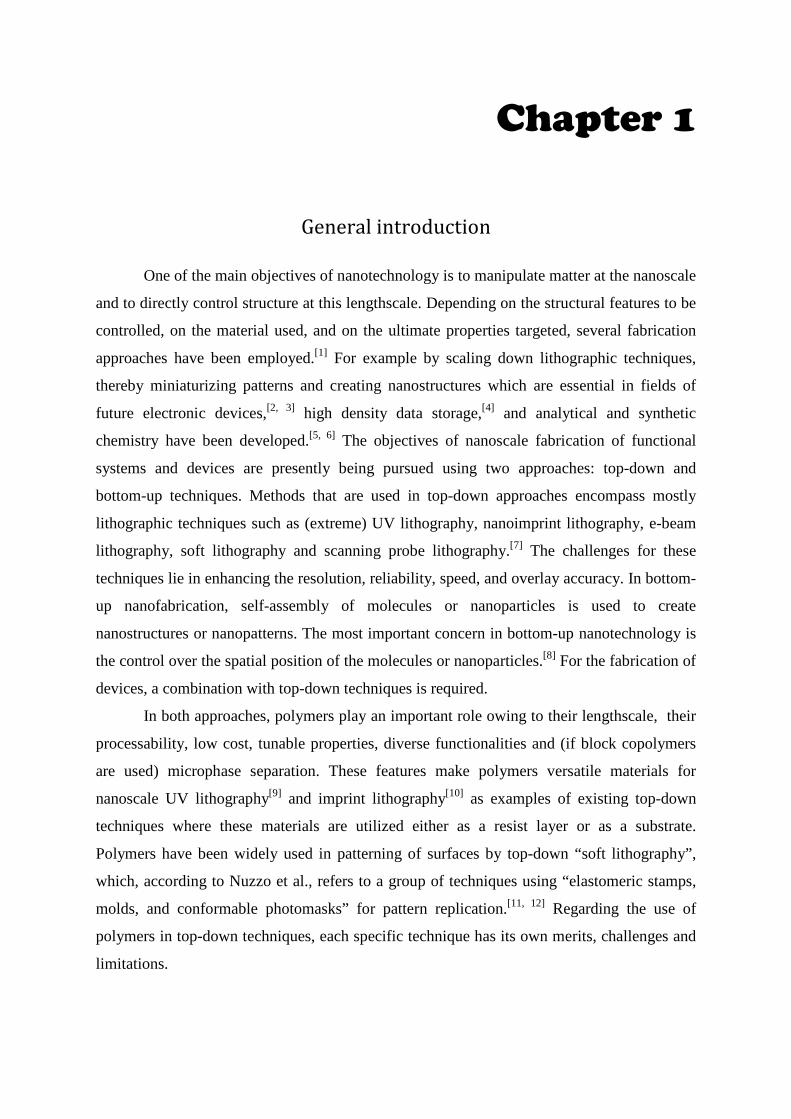
Figure 2.1 Photolithographic methods using masked irradiation and a negative photoresist
material: (a) Patterning by single exposure, (b) patterning by layer-by-layer coating and
exposure, (c) tilted patterning by single inclined exposure, (d) patterning by double inclined
exposure, (e) tapered patterns by rotating tilted exposure. [22]
Recently, photolithographic approaches have been extended to generate more
complex structures including high aspect ratio, tilted, suspended, or curved geometries
(Figure 2.1).[22] In conventional lithography, the mask and resist film are perpendicularly
aligned with respect to the irradiation source. By tilting the mask and resist film with respect
to the beam using a tilting stage, inclined structures can be fabricated (Figure 2.1c). Han et al.
showed the generation of bridges, embedded channels, and V-grooves with aspect ratios >4
using SU-8 (epoxy-based negative photoresist) and a conventional UV mask aligner (Figure
2.2a).[23] More complex 3D structures can be fabricated with three or four times inclined UV
exposures along different axes (Figure 2.1d).[24, 25] Inclined micro-pillars with an aspect ratio

Conventional and Alternative Lithography Techniques for the Fabrication of Nanostructures
11
of 20 (Figure 2.2b) were fabricated using a two-axes exposure method with four backside
exposures but the multi-exposure process can generate heavy UV dose domains which could
cause distortions. Tapered structures with nonvertical sidewalls can be also obtained if the
photomask and substrate with photoresist are tilted and rotated simultaneously during
irradiation as shown in Figure 2.1d and the SEM image in Figure 2.2c.[23]
Figure 2.2 SEM images of (a) tilted SU-8 patterns,[23] (b) patterns by double inclined
exposure,[24] (c) tapered patterns by rotating tilted exposure.[23]
2.2.2 Serial Writing with Charged Particles
Serial writing with electrons or ions is a lithographic technique with low throughput,
high cost and only suited for small area fabrication. These techniques provide, however,
flexibility in feature design making them attractive in academic research.
2.2.2.1 Electron Beam Lithography
In typical e-beam lithography, a beam of electrons is used to expose an electron
sensitive resist. The electrons generate secondary electrons with relatively low energy to form
free radicals and radical cations, which interact with the surface of a layer of resist, such as
poly(methyl methacrylate) (PMMA). Interaction of the electron beam with the resist causes
local changes in its solubility, and in the case of PMMA, the electrons will locally induce
chain scissions that makes the polymer soluble in a developer. PMMA was one of the first
polymers recognized to exhibit sensitivity to electron beam radiation and is nowadays the
most frequently used polymer in e-beam lithography.[22]
The resolution is limited because of the electron scattering of primary and secondary
electrons in the resist even though electron wavelengths on the order of 1Å can be achieved.
Patterns with features as small as ~50 nm can be generated by this technique.
[26]
E-beam lithography is impractical for mass production because of long writing times.
Therefore, it is mainly used to produce photomasks in optical lithography or to produce small

Chapter 2
12
numbers of nanostructures for research purposes. It is also used in the areas where optical
lithography fails such as for the fabrication of high frequency GaAs field-effect transistor
(FET) devices that require a resolution down to ~100 nm.[27]
2.2.2.2 Ion Beam Lithography
This method includes a variation of the electron beam lithography technique, using a
focused ion beam (FIB) instead of an electron beam. High energy ions, such as Ga+, H+, or
He+ are able to penetrate a resist material with well defined paths. The penetration depth
depends on the ion energy. Ion-electron interactions do not result in significant deviation of
the trajectory of the ion from the straight line path. Therefore high aspect ratio structures with
vertical side walls can be fabricated. Similar to e-beam writing, the low energy secondary
electrons initiate chemical reactions.[22]
The utilization of a focused mega-electron-volt (MeV) proton beam to write accurate
high-aspect-ratio walls of 30 nm width with sub-3 nm edge smoothness has been reported.[28]
Typically, a MeV proton beam is focused to a sub-100 nm spot size and scanned over a
suitable resist material. When the proton beam interacts with matter it follows an almost
straight path. The secondary electrons induced by the primary proton beam have low energy
and therefore limited range, resulting in minimal proximity effects. These features enable
smooth three-dimensional structures to be directly written into resist materials. The technique
is named p-beam writing.[28]
2.3 ALTERNATIVE LITHOGRAPHIES
Photolithography has circumvented many limitations during its development and is
widely used to fabricate nanostructures.[29, 30] However, the limitations based on the physics
of diffraction and interactions of high energy photons are hard to overcome. This technique
cannot easily be performed on polymeric or curved substrates and cannot pattern large areas
with high resolution in a single step. It also has the disadvantage of high capital and
operational cost. Hence in order to accomplish smaller features at a lower cost, new
patterning techniques are being explored and developed. Some of the oldest and conceptually
simplest forms of plastics macroscale processing (embossing, molding, stamping, or printing
are now being re-examined for their potential adaptation to nanofabrication. In the molding
technique, the surface relief of a hard stamp or mold is transferred into a soft material.
Several methods have been developed in the past decade to obtain micro- and nanostructured
polymer surfaces using molding or related strategies. Some of them are i) temperature-based
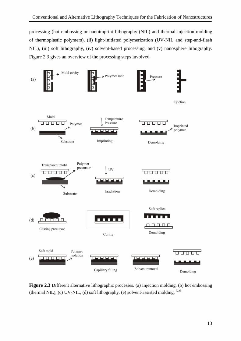
Conventional and Alternative Lithography Techniques for the Fabrication of Nanostructures
13
processing (hot embossing or nanoimprint lithography (NIL) and thermal injection molding
of thermoplastic polymers), (ii) light-initiated polymerization (UV-NIL and step-and-flash
NIL), (iii) soft lithography, (iv) solvent-based processing, and (v) nanosphere lithography.
Figure 2.3 gives an overview of the processing steps involved.
Figure 2.3 Different alternative lithographic processes. (a) Injection molding, (b) hot embossing (thermal NIL), (c) UV-NIL, (d) soft lithography, (e) solvent-assisted molding. [22]
Chapter 2
14
2.3.1 Mold Fabrication
Mold fabrication is the most time- and cost-consuming step and one of the largest
limitations in industrial application.[31] For this reason, a master is fabricated and copies of
the master in other hard materials are preferentially used as molds for imprinting. High
resolution 3D stamps are fabricated by e-beam lithography and dry etching, while shallow
stamps by e-beam lithography and metal lift-off can be obtained.[32] A widespread choice of
stamp material is Si with an oxide layer on top.[33, 34] Masters of Si are fabricated by reactive
ion etching techniques [35] or deposition of nickel and other metals on patterned resist
substrates. Small features with sub-20 nm dimensions have been achieved by electron beam
lithography and lift off.[36] An optimized double-layer resist system allowed the formation of
a Cr etching mask of 15-20 nm in diameter. However, the metal roughness was found to be a
problem for sizes below 10 nm due to the crystal grain structure of the evaporated metal.[37]
Selecting the mold material should be carefully done and issues such as hardness,
compatibility with other microfabrication processing and thermal expansion coefficients must
be considered. Diamond[38] and lithium[39] have been investigated as potential mold materials
for NIL by some groups. Taniguchi et al. used a spin-on-glass (SOG) material, which is
almost the same as quartz in composition, as a material for hard stamps.[40] The SOG acted as
a positive-tone electron beam resist and nanopatterns were fabricated by using e-beam
lithography (EBL). The obtained pattern was directly usable as a nanoimprint mold without
the risk of etching.
EBL has been established as a useful method for production of masters but so far lacks
the commercial viability due to the high cost related to the exposure procedure. Etching of
poly(tetrafluoroethylene) (PTFE) using synchrotron radiation has also been shown to perform
3D fabrication of masters.[41] Owing to its thermostability, resistance to chemicals and its
very low adhesion, PTFE may be one of the most suitable materials for molding polymers,
however PTFE is notoriously difficult to process. Processing of 1000 µm height structures by
synchrotron radiation takes about 10 min, much shorter than achieved by X-ray lithography.
Due to the directional emission of synchrotron radiation, high aspect ratio structures can be
easily created.
In order to facilitate mold release, antisticking surface coatings are being used. These
layers lower the surface tension of the mold surface and reduce adhesion. Different strategies
can be employed: (i) use of fluoropolymer films deposited (noncovalently bonded) on the
stamps with the help of a plasma treatment; (ii) treatment of silicon masters with
perfluorosilanes, e.g., 1H,1H,2H,2H-perfluorodecyltrichlorosilane;[42] and (iii) treatment of

Conventional and Alternative Lithography Techniques for the Fabrication of Nanostructures
15
Ni or alumina stamps with fluorinated alkyl phosphoric acid derivatives.[43] Alternatively,
molds made of fluoropolymers, such as PTFE, can be used. These molds are fabricated by
casting a fluoropolymer solution on the master followed by drying, or imprinting the
fluoropolymer melt.
One of the many advantages of molding is that it does not use light energy beams, and
therefore, its resolution is not limited by the effects of wave diffraction, scattering, or back
scattering from the substrate.[30] The same mold can be used several times to fabricate
nanostructures which makes it a low cost technique. The availability of a suitable mold and
the possibility of removing the molded material from it without damage are the prerequisites for
molding.
2.3.2 Nanoimprint Lithography: Embossing Thermoplastic Materials
The principle of nanoimprint lithography[7, 33, 34] (hot embossing) and thermal
injection is that a hard mold containing nanoscale features on its surface is used to deform a
thermoplastic polymer deposited on the wafer substrate under controlled temperature and
pressure (Figure 2.3b).[44] Increase of the temperature of the polymer reduces the viscosity of
the material so that pressure application causes the polymer melt to flow into the cavities of
the mold. The subsequent cooling of the system freezes the pattern on the target surface, thus
providing a negative copy of the master.
Injection molding and hot embossing differ in their applications and process
conditions. In injection molding, a polymer melt is injected at high pressure into a cavity
where it cools and hardens (Figure 2.3a). In NIL, polymer sheets are compressed between the
plates of an embossing press against the mold. Since imprint lithography makes a replica of
surface patterns, the resist materials used in imprinting should be deformable under the
applied pressure.[33, 45] In NIL, typically a thermoplastic material is used as the imprinting
resist and a suitable imprint temperature is chosen which is above the glass transition
temperature of the material. It has been shown that an optimal imprinting temperature is 70-
80 oC above the Tg of the material used,[46] to ensure the polymer has a sufficiently reduced
viscosity so that imprinting can be performed at a reasonable pressure. Raising the
temperature above the Tg of the polymer causes a significant drop in both Young’s modulus
and the viscosity. The viscosity of a polymer material not only depends on the temperature,
but also strongly on the polymer molar mass. In practice, low-molecular weight polymers can
be imprinted at lower temperatures, lower pressures, or within shorter times.[47] A high
imprint pressure is needed for resist viscosities of 1000 Pa s and more to provide conformal

Chapter 2
16
contact between substrate and stamp over large areas. Thin polymer layer can be chosen
where cavities are only partially filled, and thick layers can be used for the integration of
lenses and microfluidic channels.[48-50] A good choice of process parameters such as height,
pressure, thickness and temperature is always required to imprint polymers.
The availability of polymers such as PMMA and PS with a range of molar masses Mw
and different polydispersities is an advantage for thermal NIL, and rheological
characterization of the thermoplastic materials is available.[51] These materials are, however,
not fully optimized for the special requirements of the NIL process. One of the most
important requirements of the polymers used for NIL is that they should provide excellent
mold releasing properties during the demolding process. Commercially available polymers
can hardly satisfy this requirement. During imprinting of high aspect ratio patterns, the
imprinted polymer tends to adhere to the mold, creating pattern defects although the mould
surface is treated with an antisticking layer. In addition, a higher dry etching resistance is
desirable if the imprinted polymer pattern is to be used as a mask for further pattern transfer.
Adding a Si-containing material can address this problem.[52]
NIL can be used to mold a variety of polymeric materials and pattern features as small
as ~5 nm[53] and aspect ratios of up to ~20.[54] Arrays of 10 nm diameter and 40 nm period
holes in PMMA on either silicon or gold substrates, and 6 nm diameter and 65 nm period
holes in PMMA on silicon substrates have been fabricated by NIL (Figure 2.4a).[53] NIL was
used together with optical lithography to fabricate silicon quantum dot wires, which showed
the same behavior as those fabricated using conventional electron-beam lithography. In
addition, nanoimprint lithography was used to fabricate nanocompact disks with 10 nm
features and 400 Gbits/in2 data density—nearly three orders of magnitude higher than current
CDs (Figure 2.4b).[53] Materials that have been patterned succesfully include biomolecules,[55]
block copolymers,[56] and conducting polymers.[57] This process has been extended to pattern
components for a range of microelectronics, optical, and optoelectronic devices.[58] The
fabrication of 60-nm channel metal–oxide–semiconductor field-effect transistors on whole 4-
in wafers using NIL was presented. The nanotransistors exhibit excellent operational
characteristics across the wafer.[59]
Nanoimprint lithography has made great progress in a relatively short time but there
are still some challenges related to this technique, one of which is the lifetime of the mold.
Nanoimprint molds have to be replaced after ~50 consecutive imprints. High pressures and
heating and cooling cycles cause stress and wear on the nanoimprint mold. Room temperature
nanoimprint lithography[60] has been developed to overcome this problem. Spin-on-glass[61]

Conventional and Alternative Lithography Techniques for the Fabrication of Nanostructures
17
or hydrogen silsequioxane[62] have been used as resist materials at room temperature
nanoimprint lithography. Some different approaches have also been developed targeting the
problems mentioned above. One of the approaches is reverse nanoimprint lithography[52]
which employs a polymer film spin-coated onto the mold rather than on the substrate. The
produced film can be transferred from the mold to the substrate by NIL (Figure 2.4c). This
technique was performed by using PMMA and Figure 2.4c shows imprinted PMMA patterns
with 350 nm line spacing. This technique can also be used to transfer patterns onto substrates
that are not suitable for spin-coating or have surface topographies, which have been a long-
standing problem in imprint-based lithography.[63] Multilayer resist approaches with a thick
planarization layer on top of the non-flat substrate have been used to solve this problem but
these approaches require complex processes with multiple steps and need deep etching
through the thick planarization layer.[64] Reverse imprinting has solved this problem very
efficiently. Figure 2.4d shows polycarbonate grating structures reverse imprinted over etched
features on a Si substrate which could have potential application in chemical and biological
analysis.[63] This technique also offers the fabrication of three-dimensional structures by a
layer-by-layer approach. Figure 2.4e demonstrates the imprinted three-layer nanostructure,
using three different polymers. The imprinting results depend on several parameters such as
Tg of the polymers, film thickness, width and height of the features on the substrate, and
mechanical properties of the polymers.[63]

Chapter 2
18
Figure 2.4 (a) SEM image of holes imprinted into PMMA.[53] (b) SEM image of a 40 nm
track of a nano-CD fabricated by NIL and metal lift-off.[53] (c) Schematic of reverse
nanoimprint and SEM of reverse imprinted PMMA gratings with 350 nm line
width/spacing.[63] (d) SEM image of polycarbonate grating structures imprinted with reverse
imprinting.[63] (e) SEM image of an imprinted three-layer nanostructure, using three different
polymers.[63]
A high viscosity of the polymer film presents another challenge for nanofabrication
using NIL. An optimal pattern size and feature density should be provided for NIL.[65]
Embossing micrometer–scale features can be more challenging than nano-scale features since
filling large areas within the mold requires more lateral displacement of the polymer than
smaller features and thus the processing time increases. The thickness of the residual layer
can also vary across the imprinted region depending on the pattern density or layout of the
patterns. Residual layer non-uniformities present a challenge for transferring the pattern
uniformly into the underlying substrate.[1]
During imprinting, the resist is displaced by squeeze flow and capillary forces.[66] The
flow phenomena have been investigated by use of specific test patterns, for example negative
and positive stamps or stamps with different pattern sizes. It was found that large patterns are
much harder to be filled completely than small patterns. This is due to the polymer having to
be transferred over large distances in the case of micrometer sized structures.
Combination of NIL with other patterning techniques allows the fabrication of 3D
structures.[67] It has been shown that performing a step of imprinting into a PMMA film and

Conventional and Alternative Lithography Techniques for the Fabrication of Nanostructures
19
utilizing that prepatterned polymer layer as a resist for X-ray lithography provides a flexible
method to fabricate a wide class of complex small-scale 3D structures (Figure 2.5).
Figure 2.5 3D patterns obtained by combining X-ray lithography with NIL. The scale bar
represents 10 µm.[67]
NIL has also been combined with photolithography to replicate structures in negative
tone resists by introducing a hybrid mask concept which is made of UV transparent material
and acts both as a NIL mold and as a photolithography mask.[52] A further improvement has
been made by placing a metal layer on top of the mold so that exposure of the resist layer
underneath could be prevented while unexposed residual layer can be removed easily in a
developer solution. This can eliminate the residual layer removal step in NIL completely and
could simultaneously solve the problem associated with the non-uniformity of the residual
layer.
2.3.3 Ultraviolet-assisted Nanoimprint Lithography (UV-NIL)
UV-NIL[68] makes use of UV-curable polymeric materials for imprinting. In this
technique, the mold (made of quartz, indium tin oxide or hydrogen silsesquioxane)[69-71] is
pressed into the UV-curable solution at room temperature after which the solution is
photopolymerized by UV-irradiation (Figure 2.3c). Due to the low viscosity of the resist, only
low pressure is needed to press the mold into the resist. After the detachment of the mold, a
replica of the mold’s topography remains in the resist layer.
There are some advantages of UV-NIL over thermal NIL: i) UV curing is rapid,
therefore, high-throughput can be achieved; ii) it can be performed at room temperature and
low pressure; iii) the low viscosity of the polymeric precursors facilitates filling of high
aspect ratio cavities; iv) since thermal cycling is not required in UV-NIL, accurate shape
transfer can be obtained. A thin residual layer remains which is different from conventional
lithography.

Chapter 2
20
Acrylates are most often used in UV-NIL formulations, because of their commercial
availability, low viscosity, and rapid photopolymerization via radical propagation.[22]
However, the application of acrylates requires an inert atmosphere since oxygen is a strong
radical inhibitor for this process. Vinyl ethers have been proposed to replace acrylates since
their polymerization proceeds via a cationic mechanism which is insensitive to oxygen.[72]
The limitation of vinyl ether formulations is that they adhere to the substrate more strongly so
that double force is required for mold release. This is overcome by the higher tensile strength
of vinyl formulations. Figure 2.6 shows some UV-curable resists used for imprinting.
Figure 2.6 UV-curable resist components.
Shrinkage is an important parameter to be optimized to avoid rupture of the embossed
structures during demolding. During UV curing, the material shrinks by a value between 3-
15% and this facilitates demolding. However this makes pattern design and control difficult.
In order to obtain high aspect ratio structures the UV irradiation should be controlled.
Excessive UV curing causes excessive shrinkage and brittleness of the resist which also
results in cracking and breaking during demolding. Insufficient UV curing leads to low
cohesive strength of the polymer and causes distortion and collapse of the structures.[73] A
profound analysis of the factors such as UV polymerization time, vertical walls and surface
energy of the mould, surface roughness, and resin transparency affecting replication and
demolding during UV-NIL have been reported.[73, 74]

Conventional and Alternative Lithography Techniques for the Fabrication of Nanostructures
21
Jung et al. have developed a UV-NIL process to fabricate 34×34 crossbar circuits with
a half-pitch of 50 nm.[75] In this process, a new resist formulation including benzyl
methacrylate monomer and irgacure (photoinitiator) was used to overcome the shrinkage
problem during curing and to minimize the residual layer thickness. The problem of trapped
air during contact with the mold was solved by changing the surface energy of the substrate.
Step-and-flash imprint lithography (SFIL),[76, 77] a UV-NIL variant, uses a
photocurable prepolymer solution as a material to replicate the topography of a mold. In
SFIL, a low viscosity, photocurable liquid or solution is not spin-coated but dispensed in the
form of small droplets onto the substrate to fill the voids of the quartz mold. The solution
contains a low-molecular-molar mass monomer and a photoinitiator. Exposing this solution
to UV light cures the photopolymer to make a solidified replica while in contact with the
mold. Removing the mold leaves the inverse replica on the substrate. Because of the ability to
pattern at room temperature and at low pressure, the template can be stepped to pattern the
whole wafer area as in a stepper lithography tool. Examples of imprinted features by SFIL are
shown in Figure 2.7a-d.
Figure 2.7 SEM images of imprinted images by the S-FIL process: (a) 50 nm dense lines, (b)
20 nm semidense lines, (c) 60 nm posts, and (d) three-tiered structures. (e) SEM image of an
S-FIL replicated structure (the inset scale bar shows 80 nm lenses on the surface).[77, 78]
SFIL avoids incomplete mold filling by using monomeric fluids with a low viscosity.
However, complete displacement of the fluid by the mold is prevented by hydrodynamic
forces resulting in a residual layer of cured material between patterned features.[1, 78] The
substrate and the mold should be parallel and flat enough to obtain a uniform residual layer
over the entire imprinted area. The residual layer can be removed via etching.
Chapter 2
22
Fluid dynamics is an important issue in the SFIL process.[79] There are several
parameters that govern fluid flow of the liquid monomer between the substrate and the
template. Parameters governing the fluid flow include the number of initial monomer drops
and the relative volume of drops dispensed, flow front arrest at edges of high aspect ratio
features and template edges, air entrapment during feature filling, template velocity and force
used for imprint, and imprint time.
Pattern density is not a problem for this technique in contrast to thermal NIL.[66, 80]
The imprint quality for thermal NIL is limited by the differences in pattern size which is not
the case for SFIL since a low viscosity fluid is used. However, shrinkage as a result of
polymerization must be controlled since this could affect the size, shape and the placement of
the replicated structures.
By using an SFIL multilayer method, PMMA lines of 60 nm with an aspect ratio of 6
and 80 nm lines with an aspect ratio of 14 were reported in early publications.[30] Multilayer
device fabrication is possible since distortions caused by differential thermal expansion are
not an issue. This process can pattern dielectric gates for the fabrication of a metal oxide
semiconducter field-effect transistor (MOSFET) and is also being developed to pattern
curved surfaces and topographies in a single step. The fabrication of contact holes of 80 nm
was demonstrated which is a significant advance in high density semiconducter devices.[78]
The ultimate resolution of replication by SFIL is unknown but it has been limited by
the size of the structures created on the template. Different methods have been employed to
fabricate templates, one of which is the use of EBL which requires several processing steps:
application of resist onto a fused silica substrate, electron beam exposure, resist development,
oxygen plasma etching, chrome etching, resist stripping and fused silica dry etching.[70, 76] In
another process, a conductive and transparent layer of indium tin oxide on the glass substrate
was incorporated to suppress charging for SEM inspection, and the UV characteristics of the
final template were affected minimally which resulted in features as small as 30 nm.[78] In
another template fabrication process, to eliminate the etching process, a film of hydrogen
silsesquioxane (HSQ) was spin-coated on the ITO layer and then directly written with e-beam
lithography. The use of HSQ for direct patterning of SFIL template structures is very
convenient since it becomes a durable oxide in its cured state.[71] The use of Focused Ion
Beam (FIB) writing as an alternative process to EBL has been demonstrated for the
fabrication of 3D structures for SFIL templates which reduces the number of aforementioned
lithography steps.[81] As an example, Figure 2.7e shows a fabricated array of concave
Motheye lenses employing FIB and then replicated through SFIL imprinting.

Conventional and Alternative Lithography Techniques for the Fabrication of Nanostructures
23
2.3.4 Soft Lithography
Soft lithography refers to a collection of pattern replication methods that rely on an
elastomeric mold.[8] The process can be separated into two parts: fabrication of elastomeric
elements by casting and thermal curing of a liquid prepolymer on a master and the use of
these elements as a mold or stamp in a subsequent patterning process (Figure 2.3d). A
number of polymers can be used for molding. Elastomers such as poly(dimethylsiloxane) or
PDMS (for example, Sylgard 184, Dow Corning) are a versatile class of polymers for
replication of the master.[82] PDMS has a number of useful properties for nanofabrication as it
is durable, inert to most of the materials being patterned or molded and chemically resistant
to many solvents. Despite the advantages of PDMS, the material also suffers from high
compressibility which causes shallow relief features of a stamp to deform, buckle, or collaps,
in addition, these relief structures tend to deform upon release from the master because of
surface tension.[83-86] Other elastomers tested as pattern transfer elements are polyurethane,
polyimide, and cross-linked Novolac resins. A new class of fluoropolymers called
perfluoropolyethers (PFPE) are used to replace PDMS owing to their excellent release
properties and resistance to swelling by organic solvents and monomers. A microfluidic
device based on PFPE was fabricated and tested by using different solvents, thus proving its
potential in the field of microfluidics.[87]
Microcontact printing (µCP), a soft lithography technique,[88, 89] transfers molecules
from a patterned PDMS stamp to a substrate by the formation of covalent bonds.[90-92] It was
mainly developed for self-assembled monolayers (SAMs) of alkanethiols on gold and silver.
In this process, an elastomeric PDMS stamp inked with an appropriate solution of an
alkanethiol, is brought into contact with the surface of a substrate to transfer the ink
molecules to those regions of the substrate that contact the stamp. The flexibility of the
PDMS stamp and the conformal contact between the stamp and the surface of the substrate
are both advantageous for printing over large areas and on curved surfaces. The patterned
SAMs can be used either as resists in selective wet etching[92] or as templates[93, 94] in
selective deposition to form patterned structures of a variety of materials: metals, silicon,
organic polymers.[9, 95]

Chapter 2
24
Figure 2.9 Schematic illustration of the µCP procedure.
High aspect ratio (HAR) patterns were obtained by direct casting of PDMS onto a
mold prepared by using excimer laser perforating into wax films coated on glass or metal.
Micro-hairs of PDMS (post dimensions of 30 µm) were manufactured with aspect ratios of
up to 20 (Figure 2.8a).[96] However, thinner size posts obtained were curved in spirals due to
the capillary effects and air being trapped in the holes. X-ray LIGA (a German acronym for
lithography, electroplating, and molding) molds have also been used to fabricate HAR
structures from PDMS with an aspect ratio of 15.[97] The low Young’s modulus of PDMS
limits its use in HAR patterning of submicrometer structures. Soft elastomeric features are
affected by gravity, adhesion, and capillary forces and may collapse, generating defects in the
pattern formed.[9] To improve the mechanical stability of elastomeric stamps, alternative
materials have been proposed such as composite PDMS,[98] UV-curable PDMS[99] and
photocurable fluorinated organic-inorganic hybrids.[100]
Figure 2.8 SEM images of (a) an array of microposts in PDMS, (b) and (c) replicas in acrylic
resin obtained after soft molding with PDMS (the scale bars in (b) and (c) represent 10
µm).[96]
Soft molding includes the patterning techniques based on flexible PDMS stamps and
has some advantages over molding with hard masters. The demolding step is facilitated by
the elasticity and low surface energy of PDMS which also gives the possibility to replicate

Conventional and Alternative Lithography Techniques for the Fabrication of Nanostructures
25
the size and shape of the features present on the mold by mechanical deformation. Multiple
PDMS molds can be inexpensively fabricated from a single master.[101]
There are different molding processes depending on the material to be molded by
PDMS and the hardening mechanism. One of these is solvent-assisted micro-molding where
the polymer solution is drawn into the cavities of the PDMS mold by capillary forces (Figure
2.3e). The others are mainly UV molding of polymer films and micromolding in capillaries
(MIMIC).[1, 101]
Soft lithography is relatively cheap and flexible and allows one to control surface
chemistry which can be modified by plasma treatment and reaction with organosilanes. This
makes the technique very useful when complex organic functional groups are needed in
chemistry, biology or biochemistry. Replication of 3D structures is possible because of the
softness and elasticity of PDMS. Structures created with an acrylic polymer using
multiphoton absorption polymerization (MAP) were replicated by microtransfer molding
using a PDMS stamp (Figure 2.8b and c). It is not possible to use microtransfer molding to
replicate every structure generated by the MAP technique but careful study of the effects of
peeling rate and angle of PDMS stamp removal could increase the reproducibility.[102]
2.3.5 Colloidal Lithography
Colloidal lithography uses particles which are an attractive tool for nanofabrication
due to their ability to self-organize. The self-assembled particles have been used in the
fabrication of nanopatterns and lithographic masks. Colloidal lithography is inexpensive,
inherently parallel, high-throughput, and has a high materials versatility. It is capable of
producing well-ordered, 2D-3D periodic arrays of nanoparticles from a variety of materials
on many substrates. Three dimensional layers are of interest for photonic applications,
whereas two-dimensional layers are used as etch or lithographic masks.[103]
2.3.5.1 Synthetic Methods to Prepare Colloidal Particles
Various polymerization methods such as emulsion, dispersion, precipitation and
suspension polymerization can be used to synthesize polymer colloidal particles.[104] Polymer
particles such as polystyrene (PS) and poly(methyl methacrylate) (PMMA) are commonly
synthesized by emulsion and dispersion polymerization. The particle sizes vary in the range
of 0.05 to 10 µm depending on the reaction conditions. For emulsifier-free emulsion
polymerization,[105] the reaction temperature and the monomer concentration are the most
important factors that control the size of the particles. Increase of the temperature and a

Chapter 2
26
decrease of the monomer concentration give rise to a decrease of the particle size since the
solubility of the monomer in the aqueous phase depends on the temperature, and the
depletion time of the monomer varies with the monomer concentration. The seed
polymerization method[106] can be used for monodisperse polymeric spheres larger than 1 µm
in diameter. Larger polymer particles are produced by additional repeated polymerization
onto the seed polymer latexes which broadens the polydispersity due to the repeated addition
of the raw materials. A single-step dispersion polymerization is generally used as an
alternative to produce larger particles. In dispersion polymerization, the reaction site is a
monomer droplet stabilized by a smaller amount of surfactants and an initiator, which is
soluble in oil and diffuses to the monomer droplets which act as a bulk polymerization
reactor.[103, 107]
Stöber et al.[107] developed a technique to prepare inorganic oxide particles, for
example silica particles, by using sol-gel chemistry. It is based on the hydrolysis and
condensation of tetraethylorthosilicate (TEOS) in a mixture of alcohol, water and ammonia.
Synthesis of inorganic particles is achieved following two steps which are nucleation and
subsequent growth. To obtain monodisperse particles, these two steps should be separated
such that the nuclei can be homogeneously generated without simultaneous growth. In
general, the size and polydispersity of particles are related to many factors such as pH, the
concentration of the catalyst, the composition of reagents, the type of solvent, and the
reaction temperature, which all affect the rates of hydrolysis and condensation.[108]
The principles involved in the preparation of particles have been described[109] and it
is now possible to obtain uniform metal oxides, halides, sulfides, selenides, phosphates,
carbonates, etc. in different morphologies. Properties of these powders can be modified either
by producing solids of internally mixed composition or by coating cores with shells of a
different compound.[109]
2.3.5.2 Methods of Colloidal Crystal Assembly
Dispersion stability and the crystallization of the colloidal dispersion are governed by
interactions including Van der Waals forces, steric repulsion, and Coulombic repulsion.
During the fabrication of colloidal templates or masks, the evaporation of solvent may induce
self-assembly of the colloidal particles which makes capillary forces important in the
arrangement of the particles.[103, 110] Figure 2.10 shows the strategies for fabricating 2D
colloidal arrays including dip-coating, floating on an interface, electrophoretic deposition,
physical and chemical template-guided self-assembly, and spin-casting.

Conventional and Alternative Lithography Techniques for the Fabrication of Nanostructures
27
In dip-coating,[111] capillary forces and controlled evaporation induce self-
organization of particles (Figure 2.10a). The quality of the self-organization is determined by
the evaporation rate, which can be controlled by a step motor which helps to lift up the
substrate from the colloidal suspension at a controlled rate such that the entire surface can be
covered by domains.
Figure 2.10 Self-assembly strategies to create ordered colloidal arrays: a) dip-coating, b)
electrophoretic deposition of colloids, c) template-guided self-organization, d) chemical or
electrochemical self-organization of colloidal particles, e) lifting up a colloidal array from an
interface using a substrate, f) spin-coating of assembled colloidal particles.
Electrophoretic deposition[112, 113] of the particles employs electric fields to move the
particles as shown in Figure 2.10b. Particle assembly takes place inside a thin layer of a
colloidal suspension sandwiched between conducting substrates such as indium tin oxide
coated glass substrates followed by applying the electric field across the electrodes.[35]
Electrophoretic movement not only accelerates the sedimentation speed of small colloidal
particles but also guides the growth of a colloidal crystal over a large area in a controlled
manner. The combination of patterned electrode templates with electric field driven assembly
was shown to control crystal packing and lattice orientation control. Hexagonal and square
type packing symmetries of 2D colloidal monolayers were obtained over large surfaces by
uisng this so called graphoepitaxy method.[113]
Defect formation can be suppressed by template-assisted self-assembly of colloidal
particles.[114] A chemically[115, 116] (Figure 2.10d) or topographically[117] (Figure 2.10c)
patterned substrate can be used for the selective deposition of colloidal particles. Physical

Chapter 2
28
templates based on relief structures patterned on the surfaces of solid substrates have been
used by Xia et al. to produce a variety of structures including polygonal, polyhedral, spiral,
and hybrid aggregates of spherical particles that are difficult to fabricate with other
methods.[117] The structure of the aggregates was controlled by changing the shape and the
dimensions of the template using conventional photolithography, which also prevented the
production of templates with feature sizes smaller than 100 nm.
Figure 2.10e shows the assembly of a colloidal array floating on an interface. The
quality and packing of the array at the interface can be controlled by changing the
concentration of the particles or electrolytes, the particle size, the surface charge and the
hydrophobicity of the particles.[118, 119] For example, silica colloids modified by silanizing the
surface to enhance the hydrophobicity were self-assembled at an octane/water interface. A
monolayer without variation in the layer thickness could be obtained which is not possible for
evaporation-induced self-assembly.[120] The Langmuir-Blodgett film technique can also be
used to obtain such a uniform layer. [121]
Another way of preparing a colloidal array is by using spin-coating.[122] The colloidal
particles organize themselves into a hexagonal array more rapidly due to the centrifugal
forces (Figure 2.10f). The thickness of the particle layer is controlled by adjusting the particle
loading and the spin speed. Spin-coating provides advantages for both scaling up and mass
production since the process is rapid and compatible with wafer processing.
2.3.5.3 Nanopatterning with Colloidal Masks
Colloidal particles in a hexagonally packed array can be used as a mask so that
deposition or etching proceeds through the interstices between the colloidal particles.
Evaporation and sputtering into these interstices has been used to produce very thin films (<
30 nm) of metals and inorganic oxides. The sputtered material can be chosen without any
limitation, and the size, height, and number density of the metal dots can be controlled by
simply adjusting the particle size and the sputtering conditions.
The use of colloidal particle arrays as masks for metal sputtering or etching substrates
was pioneered by Fischer et al. and Deckman et al.[123, 124] Duyne et al.[125] used single- or
double-layered PS particles on various substrates as a mask for metal deposition as illustrated
in Figure 2.11. As seen in Figure 2.11a and b, a hexagonally ordered triangular array of metal
dots formed from a single layer colloidal mask, and a spherical dot array with different unit
lattices was fabricated from the double-layer mask (Figure 2.11c, d). The reason for the
formation of a spherical dot array is that when a second layer of nanospheres assembles onto

Conventional and Alternative Lithography Techniques for the Fabrication of Nanostructures
29
the first, every other three-fold hole is blocked, and a smaller density of six-fold interstices
results as shown in Figure 2.11c and d.
Figure 2.11 (a) Schematic diagram of a single layer nanosphere mask and (b) a hexagonally
ordered triangular array of metal dots after removal of the template. (c) Schematic diagram of
a double layer nanosphere mask and (d) spherical dot arrays after removal of the template.[125]
Colloidal arrays as masks have also been used for the nanofabrication of various
organic and inorganic materials. The deposited materials, in some cases, can be used as seeds
for the growth of other functional materials. For instance, carbon nanotubes were grown on
nickel nanodots that were pre-deposited through a colloidal mask by using plasma-enhanced
chemical vapor deposition (PECVD) (Figure 2.12a).[126] Zinc oxide nanorod arrays were also
prepared using PS particles as a template for patterning gold catalyst particles and subsequent
bottom-up growth in a tube furnace using chemical vapor deposition (Figure 2.12b).[127]
Similarly, an organic light-emiting nanodiode (OLED) array was fabricated by deposition of
multilayers through the interstices of the particle array without causing etching damage which
is the case for conventional masking processes.[128] Patterning of ferromagnetic arrays was
demonstrated over an area greater than 1 cm2 without agglomeration of particles after metal
evaporation which gave control over the diameter, aspect ratio, and pitch of the fabricated
elements.

Chapter 2
30
Figure 2.12 (a) Vertically aligned carbon nanotube array by using plasma-enhanced chemical
vapor deposition (PECVD).[126] (b) ZnO nanorod arrays prepared using gold catalyst particles
and subsequent bottom-up growth in a tube furnace using chemical vapor deposition[127] (c)
SEM image of silicon nanopillars fabricated by means of an aluminum etch mask obtained
using a PS particle array.[129] The scale bar indicates 200 nm. (d) Cross-sectional image of the
Si nanopillars after etching.
Sputtered metal arrays can be used as etching masks to create surface topography.
Silicon nanopillars with diameters as small as 40 nm and aspect ratios of up to 7 were
fabricated by preparing an aluminum etch mask using a PS particle array (Figure 2.12c).[129]
Large-area periodic silicon nanopillar arrays have been obtained after metal deposition, lift-
off, and etching processes. By varying the etching parameters, such as mask materials and
etching recipes, the size and the shape of silicon nanopillars can be modified, thus size and
shape control of nanostructures can be achieved.[129]
The combination of colloidal lithography (CL) and alkanethiol self-assembly was
used to create substrates with controlled surface topography and chemical composition.
Patterns exhibiting also chemical contrast allow one to investigate the interfacial interactions
or adsorption behavior of biomolecules and nanoparticles. For example, Michel et al. created
topographical contrast via colloidal patterning to design platforms for the attachment of
targeted proteins.[130] Nanopillars of TiO2 (50-90 nm in diameter, 20 nm in height) on
oxidized silicon were fabricated by using colloidal lithography and were then rendered
hydrophobic by the selective self-assembly of an organophosphate, whereas a poly(ethylene
glycol)-grafted copolymer was adsorbed onto the surrounding SiO2, rendering it protein
resistant. Further binding of streptavidin onto the organophosphate and immobilization of
biotinylated liposomes to the streptavidin was accomplished successfully.[130]
Tan et al.[131] used particle arrays as a mask to fabricate a dome structure by reactive
ion etching [35] which converts the spheres into nonspherical particles. Single and double
layers of packed colloidal polystyrene microspheres of uniform size (diameter 1.2 µm) were
spin-coated onto cleaned Si substrates, which were then exposed to CF4 and O2 plasma

Conventional and Alternative Lithography Techniques for the Fabrication of Nanostructures
31
mixtures. Due to preferential etching in the direction normal to the surface of the substrate,
the microspheres were reduced to a nonspherical form resembling a biconvex microlense
(Figure 2.12d).
Spherical colloidal particles can be utilized for preparing various types of porous
materials that exhibit precisely controlled pore sizes and highly ordered 3D porous structures.
After drying the colloidal array, the voids between the colloidal spheres are fully infiltrated
with a liquid precursor such as an ultraviolet [132] or thermally curable organic
prepolymer,[109] or an ordinary organic monomer (plus an initiator).[133] Subsequent
solidification of the precursor and removal of the colloidal spheres gives a 3D porous
structure. Johnson et al.[133] prepared ordered mesoporous polymers by filling the pores in the
colloidal crystals (silica spheres of 35 nm in diameter) with divinylbenzene (DVB),
ethyleneglycol dimethacrylate (EDMA), or a mixture of the two. Polymerization and
subsequent dissolution of the silica template left a polycrystalline network of interconnected
pores. When mixtures of DVB and EDMA were used, the pore size of the polymer replicas
varied continuously between 35 and 15 nm because the polymer shrinks when the silica
template is removed.[133] Initiated chemical vapor deposition (iCVD) has also been used to
produce grafted polymeric layers (Figure 2.13).[134] Patterns were generated for a broad range
of materials including organic polymers (pBA, pHEMA), fluoropolymers (pPFDA, pPFM)
and organosilicones. Since iCVD is a solvent-free process, it has many advantages compared
to solution polymerization.[134]
Figure 2.13 Schematic process to produce polymeric nanostructures using CL. A
hydroxylated substrate was treated with a vapor-phase silane coupling agent, which
covalently attaches the vinyl groups to the substrate in the exposed regions of the colloidal
mask. The polymer was grafted and the grafted film was sonicated to remove the colloidal
template, leaving an array of bowl-shaped nanostructures.
2.3.5.4 Modification of Colloidal Masks
One of the disadvantages of the CL method is the limited control over the shape of the
patterns, which is triangular or spherical. Adjustment of the deposition method and
modification of the colloidal masks have been suggested to overcome this limitation.[103] The

Chapter 2
32
deposition method can be modified by tilted or rotated deposition through the as prepared
colloidal mask. The angle between the deposition flow and the substrate normal can be
controlled and a variety of structures (elongated triangles or double triangles) has been
obtained by varying this angle. However, the shapes obtained are restricted by the mask
shape.[103]
A more effective approach is to modify the colloidal particles by suitable post-
treatment such as RIE, ion milling, or annealing. The deformation of polymeric beads such as
PS and PMMA occurs above the glass transition temparature and this has been utilized to
modify the colloidal mask for fabricating a gold disk array via CL. The size of the disk was
adjusted by changing the annealing time, since polymeric particles spread over a wider
distance with the annealing time (Figure 2.14a-f). Microwave heating can also be used to
anneal the polymer particles which gives more precise control over the degree of
annealing.[135] Kosiorek et al. produced particles with morphologies such as rings, rods, and
dots by changing the mask morphology by temperature processing and varying the
evaporation conditions.[135] The technique was shown to scale down the size of metallic
nanoparticles from 200 to 30 nm, while preserving the original nanospheres pacing and order.
It was shown that by temperature treatment it is easy to control the spaces between the
spheres, and therefore the size of the particles deposited through the PS mask.
Meanwhile, RIE has been used to modify the colloidal mask by changing the size and
the shape of the particles.[136] RIE has been employed to control the surface morphology and
roughness and to enhance the surface hydrophilicity in polymeric and biological applications.
RIE was used to fabricate polymeric nanofibrillar surfaces and patterned structures using
colloidal single layers and double layers. Choi et al. have created well organized layers of
nonspherical colloidal particles by using anisotropic RIE of the spherical polymer latexes that
were stacked layer-by-layer, with the top layer acting as a mask.[137] The shadowing effect
from the upper layer of particles to the layers beneath resulted in nonspherically etched
polymeric structures (Figure 2.14g). The resulting patterns and particle shapes were
dependent on the crystal orientation relative to the substrate (Figure 2.14h), the number of
colloidal layers, and the RIE conditions.

Conventional and Alternative Lithography Techniques for the Fabrication of Nanostructures
33
Figure 2.14 A 540-nm PS latex mask annealed in 25 mL of a water/EtOH/ acetone mixture
by a) 1, b) 2, c) 4, d) 6, e) 7, and f) 10 microwave pulses.[135] g) Binary particle arrays and 2-
D nanopatterns produced from a double layer of small PS beads (200 nm). h) Ternary particle
arrays produced after partial RIE etching of PS beads in fcc symmetry.[137]
2.4 SURFACE STRUCTURING with ORGANOMETALLIC POLYMERS
Poly(ferrocenylsilane)s (PFSs) composed of alternating ferrocene and silane units in
the main chain, belong to the class of organometallic polymers. High molar mass
poly(ferrocenylsilane) macromolecules were discovered in the early 1990s by Manners et
al.[138] by thermal-ring opening polymerization of highly strained, silicon-bridged
[1]ferrocenophanes. There are several ways to polymerize silicon-bridged [1]ferrocenophanes
such as by use of anionic initiators,[139] transition metal catalysts[140, 141] or in the solid state
using a 60C γ-ray source[142] (Figure 2.15). The physical properties of PFS depend on the
substituents at silicon. Symmetrically substitued PFSs are often semicrystalline,[143] whereas
asymmetrically substitued PFSs are, in general, amorphous.[144] Several types of PFSs bearing
alkyl, alkoxy, aryloxy, and amino groups have been synthesized.[145]
Figure 2.15 Ring opening polymerization of strained dimethylsila[1]ferrocenophane.

Chapter 2
34
The presence of alternating ferrocene and silane units in the backbone renders this
organometallic polymer highly useful for applications in optics, semiconductors,
nanopatterned catalysis for carbon nanotube growth, electrochemically responsive substrates
or media, etc.[138, 145-147] One of the unique applications is their use as resists in "maskless"
lithography due to the presence of Fe and Si in the backbone which makes PFSs highly etch
resistant in reactive ion etching environments in comparison with organic polymers.[148]
Pattern transfer into various substrates by using these organometallic homopolymers as inks
in soft lithography owing to their etch resistance has been already demonstrated[149] and
silicon nanopillars with aspect ratios of 10 have also been fabricated.[149] One of the most
spectacular applications included the use of a PFS-b-PS diblock copolymer work to transfer
spherical patterns into magnetic cobalt films via stepwise etching using plasma etching and
ion sputtering steps.[150]
Organometallic compounds are known to act as an etch barrier in oxygen and oxygen
containing plasmas since the products of chemical etching with oxygen plasmas are non-
volatile and do not desorb from the surface.[148] When PFS films are exposed to oxygen
plasma, a thin Fe/Si-oxide layer forms on top of the film, as proven by XPS.[151] The XPS
spectra of poly(ferrocenyldimethylsilane) gave information regarding the atoms present at the
surface after treatment with oxygen plasma. It was shown that the carbon concentration was
reduced at the surface, while the oxygen, iron and silicon concentration increased and
aromaticity was destroyed.
Two soft lithography approaches, solvent-assisted dewetting and capillary force
lithography (Figure 2.16a), were employed to pattern PFS.[149] The use of
poly(ferrocenyldimethylsilane) as an ink in microcontact printing was not successful because
of the poor wettability of the PDMS stamp. Although the wettability of the PDMS stamps
was improved by treating the stamp with with an oxygen plasma prior to inking, PFS patterns
did not replicate fully the stamp pattern which proves that the polymer solution dewets
between the stamp and Si surface, forming continuous lines in the middle of the protruding
stamp. A chemically patterned substrate, prepared by microcontact printing, was also used as
a template to spin-coat poly(ferrocenyldimethylsilane) which directed the dewetting of the
polymer film.[148]

Conventional and Alternative Lithography Techniques for the Fabrication of Nanostructures
35
Figure 2.16 a) The scheme for capillary force lithography. b) SEM image of a substrate
patterned with capillary force lithography. c) SEM image of a substrate patterned with
MIMIC.[148]
Capillary force lithography (CFL) was also employed to pattern PFS.[148] Polymer
structures of 110 nm high and 500 nm wide were fabricated and subsequently developed by
CF4/O2 RIE. In addition, the influence of processing conditions and polymer architecture on
the pattern transfer in CFL using PFS etch resists was investigated. The patterns in CFL
experiments were fabricated by placing the PDMS mold in contact with the 20 nm thin
polymer films and keeping it for 4 h at temperatures ranging from 30 to 140 oC, under
vacuum. Polymers with low molar mass and corresponding low viscosities showed signs of
polymer dewetting, on the other hand polymers with too high viscosity did not yield patterns.
Most of the good quality patterns were prepared with polymer viscosities which fall into the
range between 50 and 1500 Pa·s.[152]
Thin films of organic-organometallic block copolymers self-assemble to form regions
that have a significantly different etching behavior. This property of PFS was used in block
copolymer lithography where structures down to 20 nm could be etched into the substrate.
PFS block copolymers were also employed to pattern thin films, as was shown by the use of
ferrocenylsilane-styrene block copolymers as templates in the fabrication of cobalt magnetic
dot arrays.[150] The organic-rich phase is quickly removed whereas the organometallic-rich
phase shows high resistance against oxygen and fluorocarbon plasmas which opens up the
possibility of transferring the patterns generated by block copolymer self-assembly in a one-
step etching process into the underlying substrate.[150]

Chapter 2
36
Phase-separated thin films of PS-b-PFS were used to synthesize carbon nanotubes
which show catalytic activity.[153] Substrates for nanotube growth were prepared by spin
coating. After spin-coating, the substrates were annealed in vacuum and subsequently treated
in oxygen plasma in order to remove the PS matrix and to form iron oxide-containing
nanoparticles. Carbon nanotube growth was then performed on the substrates using acetylene
as the carbon source.
Combining block copolymer self-assembly with long-range ordering methods would
allow nanostructures to be lithographically fabricated in precise positions on a substrate.[154]
Graphoepitaxy is a method that allows the formation of nanostructures by spin-coating a
block copolymer over surfaces already patterned with shallow grooves.[155] The effect of the
width of the grooves on pattern order has been shown and within a 300-nm-wide groove,
about nine rows of close-packed PFS features were aligned.[156] Figure 2.17a shows a top
view and cross section of a sphere array after spin-coating, annealing and etching. The top
surface shows a square symmetry in the sphere packing, and the cross section shows 11 rows
of spheres parallel to the surface of the substrate as shown 2.17b. For the smallest V grooves
with the thinnest films, a single of row spheres was formed. The commensurability between
the thickness of the layer and the plane spacing determines the packing and the size of
domains.[155] Ross et al. have also studied the locations and long range order of the PFS
microdomains by using templates of different sizes.[156]
Figure 2.17 SEM images of PS-PFS films in V grooves after 72 h annealing and etching (a)
square packing of spheres is visible in the top view, (b) the same sample as that in part a in a
cross sectional view showing a sphere array with 11 rows.[155]

Conventional and Alternative Lithography Techniques for the Fabrication of Nanostructures
37
Well controlled 1D arrays were formed by templating a spherical-morphology block
copolymer within a narrow groove. made from a hydrogen silsesquioxane resist layer
patterned using electron-beam lithography. A single row of PFS domains forms when 0.6 <
W/d0 < 1.5. where d0 is domain spacing and W is the confinement width of the channel. It was
shown in Figure 2.18 that the domains were distorted into ellipses with aspect ratio and major
axis orientation controlled by the groove width.
Figure 2.18 SEM image of PFS block copolymer domains within channels of different
confinement widths W. A single row of spheres forms for 0.6 < W/d0 < 1.5, where d0 is the
equilibrium row spacing of this block copolymer.[157]

Chapter 2
38
CONCLUSIONS
Conventional and unconvential techniques have enabled fabrication of 2D and 3D
structures ranging from several tens of nanometers to micrometer scales. Historically,
photolithography has been the dominant technique for replication despite of its resolution
limit. Photolithography continues to overcome obstacles to achieve new resolution limits
which, however, increases the cost. The high cost of conventional equipment for
nanofabrication pave the way to unconventional techniques. Unconventinal techniques for
nanofabrication are being widely accepted and they are extensively explored for research
purposes. Molding, embossing, and printing techniques provide higher resolution patterning
with high througput at a lower cost. Despite all recent progress in patterning, each patterning
method has its own specific strengths and advantages and can not meet the requirements of
all fabrication needs. In addition, the large-scale fabrication of surfaces by using reported
methods still remains a big challenge. Combining of different fabrication methods could help
the future development of devices and their performances.
2.5 REFERENCES
[1] B. D. Gates, Q. B. Xu, M. Stewart, D. Ryan, C. G. Willson, G. M. Whitesides, Chem.
Rev. 2005, 105, 1171.
[2] T. Ito, S. Okazaki, Nature 2000, 406, 1027.
[3] G. M. Wallraff, W. D. Hinsberg, Chem. Rev. 1999, 99, 1801.
[4] K. Gamo, Microelectron. Eng. 1996, 32, 159.
[5] Y. N. Xia, E. Kim, X. M. Zhao, J. A. Rogers, M. Prentiss, G. M. Whitesides, Science
1996, 273, 347.
[6] S. Y. Chou, S. J. Schablitsky, L. Zhuang, J. Vac. Sci. Technol. B 1997, 15, 2864.
[7] S. Y. Chou, P. R. Krauss, P. J. Renstrom, Science 1996, 272, 85.
[8] Y. N. Xia, G. M. Whitesides, Ange. Chem. Int. Ed. 1998, 37, 551.
[9] Y. N. Xia, G. M. Whitesides, Annu. Rev. Mater. Sci. 1998, 28, 153.
[10] D. M. Eigler, E. K. Schweizer, Nature 1990, 344, 524.
[11] R. D. Piner, J. Zhu, F. Xu, S. H. Hong, C. A. Mirkin, Science 1999, 283, 661.
[12] D. Wouters, U. S. Schubert, Angew. Chem. Int. Ed. 2004, 43, 2480.
[13] J. A. Rogers, K. E. Paul, R. J. Jackman, G. M. Whitesides, Appl. Phys. Lett. 1997, 70,
2658.
[14] J. A. Rogers, K. E. Paul, R. J. Jackman, G. M. Whitesides, J. Vac. Sci. Technol. B
1998, 16, 59.

Conventional and Alternative Lithography Techniques for the Fabrication of Nanostructures
39
[15] N. A. Melosh, A. Boukai, F. Diana, B. Gerardot, A. Badolato, P. M. Petroff, J. R.
Heath, Science 2003, 300, 112.
[16] Q. B. Xu, B. D. Gates, G. M. Whitesides, J. Am. Chem. Soc. 2004, 126, 1332.
[17] G. M. Whitesides, P. E. Laibinis, Langmuir 1990, 6, 87.
[18] G. M. Whitesides, J. P. Mathias, C. T. Seto, Science 1991, 254, 1312.
[19] W. M. Moreau, Semiconductor Lithography: Principles and Materials, Plenum, New
York, 1988.
[20] M. Rothschild, T. M. Bloomstein, R. R. Kunz, V. Liberman, M. Switkes, S. T.
Palmacci, J. H. C. Sedlacek, D. Hardy, A. Grenville, J. Vac. Sci. Technol. B 2004, 22,
2877.
[21] M. Rothschild, Mater. Today 2005, 18.
[22] A. del Campo, E. Arzt, Chem. Rev. 2008, 108, 911.
[23] M. Han, W. Lee, S. K. Lee, S. S. Lee, Sens Actuators A: Phys. 2004, 111, 14.
[24] H. Sato, Y. Houshi, S. Shoji, Microsystem Technologies 2004, 10, 440.
[25] F. Romanato, M. Tormen, L. Businaro, L. Vaccari, T. Stomeo, A. Passaseo, E. Di
Fabrizio, Microelectron. Eng. 2004, 73-4, 870.
[26] H. Elsner, H. G. Meyer, Microelectron. Eng. 2001, 57-8, 291.
[27] Y. N. Xia, J. A. Rogers, K. E. Paul, G. M. Whitesides, Chem. Rev. 1999, 99, 1823.
[28] J. A. van Kan, A. A. Bettiol, F. Watt, Appl. Phys. Lett. 2003, 83, 1629.
[29] S. Okazaki, J. Vac. Sci. Technol. B 1991, 9, 2829.
[30] M. Colburn, A. Grot, B. J. Choi, M. Amistoso, T. Bailey, S. V. Sreenivasan, J. G.
Ekerdt, C. G. Willson, J. Vac. Sci. Technol. B 2001, 19, 2162.
[31] I. Junarsa, P. F. Nealeya, J. Vac. Sci. Technol. B 2004, 22, 2685.
[32] K. Ansari, P. G. Shao, J. A. van Kan, A. A. Bettiol, F. Watt, Nuclear Instruments and
Methods in Physics Research Section B: Beam Interactions with Materials and Atoms
2005, 231, 407.
[33] S. Y. Chou, P. R. Krauss, P. J. Renstrom, Applied Physics Letters 1995, 67, 3114.
[34] S. Y. Chou, P. R. Krauss, P. J. Renstrom, J. Vac. Sci. Technol. B 1996, 14, 4129.
[35] A. E. Larsen, D. G. Grier, Phys. Rev. Lett. 1996, 76, 3862.
[36] I. Maximov, E. L. Sarwe, M. Beck, K. Deppert, M. Graczyk, M. H. Magnusson, L.
Montelius, Microelectron. Eng. 2002, 61-2, 449.
[37] C. M. Sotomayor Torres, S. Zankovych, J. Seekamp, A. P. Kam, C. Clavijo Cedeño,
T. Hoffmann, J. Ahopelto, F. Reuther, K. Pfeiffer, G. Bleidiessel, G. Gruetzner, M. V.
Maximov, B. Heidari, Mater. Sci. Eng. C 2003, 23, 23.

Chapter 2
40
[38] J. Taniguchi, Y. Tokano, I. Miyamoto, M. Komuro, H. Hiroshima, Nanotechnology
2002, 13, 592.
[39] M. T. Li, Princeton University, 2003.
[40] J. Taniguchi, K. Koga, Y. Kogo, I. Miyamoto, Microelectron. Eng., 83, 940.
[41] T. Katoh, N. Nishi, M. Fukagawa, H. Ueno, S. Sugiyama, Sens. Actuators, A: Phys.
2001, 89, 10.
[42] R. W. Jaszewski, H. Schift, P. Gröning, G. Margaritondo, Microelectron. Eng. 1997,
35, 381.
[43] M. Keil, M. Beck, G. Frennesson, E. Theander, E. Bolmsjo, L. Montelius, B. Heidari,
J. Vac. Sci. Technol. B 2004, 22, 3283.
[44] A. Fuchs, B. Vratzov, T. Wahlbrink, Y. Georgiev, H. Kurz, J. Vac. Sci. Technol. B.
2004, 22, 3242.
[45] C. M. Sotomayor Torres, Alternative Lithography, Kluwer Academic, New York,
2003.
[46] H. Schift, S. Bellini, J. Gobrecht, F. Reuther, M. Kubenz, M. B. Mikkelsen, K.
Vogelsang, Microelectron. Eng. 2007, 84, 932.
[47] L. J. Guo, Adv. Mater. 2007, 19, 495.
[48] N. Bogdanski, M. Wissen, S. Mollenbeck, H. C. Scheer, J. Vac. Sci. Technol. B 2006,
24, 2998.
[49] N. Bogdanski, M. Wissen, A. Ziegler, H. C. Scheer, Microelectron. Eng. 2005, 78-79,
598.
[50] V. Studer, A. Pepin, Y. Chen, Appl. Phys. Lett. 2002, 80, 3614.
[51] H. Schift, J. Vac. Sci. Technol. B 2008, 26, 458.
[52] L. J. Guo, J. Phys. D-Appl. Phys. 2004, 37, R123.
[53] S. Y. Chou, P. R. Krauss, W. Zhang, L. J. Guo, L. Zhuang, J. Vac. Sci. Technol. B
1997, 15, 2897.
[54] K. Ansari, J. A. van Kan, A. A. Bettiol, F. Watt, Appl. Phys. Lett. 2004, 85, 476.
[55] J. D. Hoff, L. J. Cheng, E. Meyhofer, L. J. Guo, A. J. Hunt, Nano Lett. 2004, 4, 853.
[56] H. W. Li, W. T. S. Huck, Nano Lett. 2004, 4, 1633.
[57] M. Behl, J. Seekamp, S. Zankovych, C. M. S. Torres, R. Zentel, J. Ahopelto, Adv.
Mater. 2002, 14, 588.
[58] M. T. Li, J. A. Wang, L. Zhuang, S. Y. Chou, Appl. Phys. Lett. 2000, 76, 673.
[59] W. Zhang, S. Y. Chou, Appl. Phys. Lett. 2003, 83, 1632.
[60] D. Y. Khang, H. Yoon, H. H. Lee, Adv. Mater. 2001, 13, 749.

Conventional and Alternative Lithography Techniques for the Fabrication of Nanostructures
41
[61] S. Matsui, Y. Igaku, H. Ishigaki, J. Fujita, M. Ishida, Y. Ochiai, M. Komuro, H.
Hiroshima, J. Vac. Sci. Technol. B 2001, 19, 2801.
[62] S. Matsui, Y. Igaku, H. Ishigaki, J. Fujita, M. Ishida, Y. Ochiai, H. Namatsu, M.
Komuro, J. Vac. Sci. Technol. B 2003, 21, 688.
[63] L. R. Bao, X. Cheng, X. D. Huang, L. J. Guo, S. W. Pang, A. F. Yee, J. Vac. Sci.
Technol. B 2002, 20, 2881.
[64] N. Kehagias, V. Reboud, G. Chansin, M. Zelsmann, C. Jeppesen, C. Schuster, M.
Kubenz, F. Reuther, G. Gruetzner, C. M. S. Torres, Nanotechnology 2007, 18.
[65] K. Pfeiffer, F. Reuther, M. Fink, G. Gruetzner, P. Carlberg, I. Maximov, L.
Montelius, J. Seekamp, S. Zankovych, C. M. Sotomayor-Torres, H. Schulz, H. C.
Scheer, Microelectron. Eng. 2003, 67-8, 266.
[66] H. C. Scheer, H. Schulz, Microelectron. Eng. 2001, 56, 311.
[67] M. Tormen, F. Romanato, M. Altissimo, L. Businaro, P. Candeloro, E. M. Di
Fabrizio, J. Vac. Sci. Technol. B 2004, 22, 766.
[68] M. Bender, M. Otto, B. Hadam, B. Vratzov, B. Spangenberg, H. Kurz, Microelectron.
Eng. 2000, 53, 233.
[69] W. J. Dauksher, K. J. Nordquist, D. P. Mancini, D. J. Resnick, J. H. Baker, A. E.
Hooper, A. A. Talin, T. C. Bailey, A. M. Lemonds, S. V. Sreenivasan, J. G. Ekerdt, C.
G. Willson, J. Vac. Sci. Technol. B 2002, 20, 2857.
[70] T. C. Bailey, D. J. Resnick, D. Mancini, K. J. Nordquist, W. J. Dauksher, E. Ainley,
A. Talin, K. Gehoski, J. H. Baker, B. J. Choi, S. Johnson, M. Colburn, M. Meissl, S.
V. Sreenivasan, J. G. Ekerdt, C. G. Willson, Microelectron. Eng. 2002, 61-2, 461.
[71] D. P. Mancini, K. A. Gehoski, E. Ainley, K. J. Nordquist, D. J. Resnick, T. C. Bailey,
S. V. Sreenivasan, J. G. Ekerdt, C. G. Willson, J. Vac. Sci. Technol. B 2002, 20, 2896.
[72] E. K. Kim, N. A. Stacey, B. J. Smith, M. D. Dickey, S. C. Johnson, B. C. Trinque, C.
G. Willson, J. Vac. Sci. Technol. B 2004, 22, 131.
[73] M. B. Chan-Park, Y. C. Lam, P. Laulia, S. C. Joshi, Langmuir 2005, 21, 2000.
[74] M. B. Chan-Park, Y. H. Yan, W. K. Neo, W. X. Zhou, J. Zhang, C. Y. Yue, Langmuir
2003, 19, 4371.
[75] G. Y. Jung, S. Ganapathiappan, D. A. A. Ohlberg, D. L. Olynick, Y. Chen, W. M.
Tong, R. S. Williams, Nano Lett. 2004, 4, 1225.
[76] T. C. Bailey, S. C. Johnson, S. V. Sreenivasan, J. G. Ekerdt, C. G. Willson, D. J.
Resnick, J. Photopolym. Sci. Technol. 2002, 15, 481.

Chapter 2
42
[77] M. D. Stewart, S. C. Johnson, S. V. Sreenivasan, D. J. Resnick, C. G. Willson, J.
Microlith. Microfab. Microsys. 2005, 4.
[78] D. J. Resnick, S. V. Sreenivasan, C. G. Willson, Mater. Today 2005, 8, 34.
[79] S. Reddy, R. T. Bonnecaze, Microelectron. Eng. 2005, 82, 60.
[80] H. C. Scheer, H. Schulz, T. Hoffmann, C. M. S. Torres, J. Vac. Sci. Technol. B 1998,
16, 3917.
[81] J. Kettle, R. T. Hoyle, S. Dimov, R. M. Perks, Microelectron. Eng. 2008, 85, 853.
[82] J. A. Ragers, R. G. Nuzzo, Mater. Today 2005, 50.
[83] J. N. Lee, C. Park, G. M. Whitesides, Anal. Chem. 2003, 75, 6544.
[84] E. Delamarche, H. Schmid, B. Michel, H. Biebuyck, Adv. Mater. 1997, 9, 741.
[85] A. Bietsch, B. Michel, J. Appl. Phys. 2000, 88, 4310.
[86] C. Y. Hui, A. Jagota, Y. Y. Lin, E. J. Kramer, Langmuir 2002, 18, 1394.
[87] J. P. Rolland, R. M. Van Dam, D. A. Schorzman, S. R. Quake, J. M. DeSimone, J.
Am. Chem. Soc. 2004, 126, 2322.
[88] Y. N. Xia, X. M. Zhao, G. M. Whitesides, Microelectron. Eng. 1996, 32, 255.
[89] Y. Xia, E. Kim, G. M. Whitesides, J. Electrochem. Soc. 1996, 143, 1070.
[90] A. Kumar, G. M. Whitesides, Appl. Phys. Lett. 1993, 63, 2002.
[91] A. Kumar, H. A. Biebuyck, G. M. Whitesides, Langmuir 1994, 10, 1498.
[92] Y. N. Xia, X. M. Zhao, E. Kim, G. M. Whitesides, Chem. Mater. 1995, 7, 2332.
[93] N. L. Jeon, P. G. Clem, D. A. Payne, R. G. Nuzzo, Langmuir 1996, 12, 5350.
[94] N. L. Jeon, K. Finnie, K. Branshaw, R. G. Nuzzo, Langmuir 1997, 13, 3382.
[95] N. L. Jeon, I. S. Choi, G. M. Whitesides, N. Y. Kim, P. E. Laibinis, Y. Harada, K. R.
Finnie, G. S. Girolami, R. G. Nuzzo, Appl. Phys. Lett. 1999, 75, 4201.
[96] G. J. Schmitz, C. Brucker, P. Jacobs, J. Micromech. Microeng. 2005, 15, 1904.
[97] K. Kim, S. Park, J. B. Lee, H. Manohara, Y. Desta, M. Murphy, C. H. Ahn,
Microsyst. Technol. 2002, 9, 5.
[98] T. W. Odom, J. C. Love, D. B. Wolfe, K. E. Paul, G. M. Whitesides, Langmuir 2002,
18, 5314.
[99] K. M. Choi, J. A. Rogers, J. Am. Chem. Soc. 2003, 125, 4060.
[100] D. G. Choi, J. H. Jeong, Y. S. Sim, E. S. Lee, W. S. Kim, B. S. Bae, Langmuir 2005,
21, 9390.
[101] B. D. Gates, Q. B. Xu, J. C. Love, D. B. Wolfe, G. M. Whitesides, Annu. Rev. Mater.
Res. 2004, 34, 339.

Conventional and Alternative Lithography Techniques for the Fabrication of Nanostructures
43
[102] C. N. LaFratta, T. Baldacchini, R. A. Farrer, J. T. Fourkas, M. C. Teich, B. E. A.
Saleh, M. J. Naughton, J. Phys. Chem. B 2004, 108, 11256.
[103] S. M. Yang, S. G. Jang, D. G. Choi, S. Kim, H. K. Yu, Small 2006, 2, 458.
[104] R. Arshady, Colloid Polym. Sci. 1992, 270, 717.
[105] R. H. Ottewill, J. N. Shaw, Kolloid-Zeitschrift and Zeitschrift Fur Polymere 1967,
218, 34.
[106] D. Z. Zou, L. Q. Sun, J. J. Aklonis, R. Salovey, J. Polym. Sci., Part A: Polym. Chem
1992, 30, 1463.
[107] W. Stober, A. Fink, E. Bohn, J. Colloid and Interface Sci. 1968, 26, 62.
[108] A. K. Van Helden, J. W. Jansen, A. Vrij, J. Colloid Interface Sci. 1981, 81, 354.
[109] Y. N. Xia, B. Gates, Y. D. Yin, Y. Lu, Adv. Mater. 2000, 12, 693.
[110] N. V. Dziomkina, G. J. Vancso, Soft Matter 2005, 1, 265.
[111] N. D. Denkov, O. D. Velev, P. A. Kralchevsky, I. B. Ivanov, H. Yoshimura, K.
Nagayama, Langmuir 1992, 8, 3183.
[112] M. Trau, S. Sankaran, D. A. Saville, I. A. Aksay, Nature 1995, 374, 437.
[113] N. V. Dziomkina, M. A. Hempenius, G. J. Vancso, Adv. Mater. 2005, 17, 237.
[114] B. Gates, D. Qin, Y. N. Xia, Adv. Mater. 1999, 11, 466.
[115] J. Aizenberg, P. V. Braun, P. Wiltzius, Phys. Rev. Lett. 2000, 84, 2997.
[116] H. P. Zheng, I. Lee, M. F. Rubner, P. T. Hammond, Adv. Mater. 2002, 14, 569.
[117] Y. N. Xia, Y. D. Yin, Y. Lu, J. McLellan, Adv. Funct. Mater. 2003, 13, 907.
[118] M. Kondo, K. Shinozaki, L. Bergstrom, N. Mizutani, Langmuir 1995, 11, 394.
[119] H. H. Wickman, J. N. Korley, Nature 1998, 393, 445.
[120] R. Aveyard, J. H. Clint, D. Nees, V. N. Paunov, Langmuir 2000, 16, 1969.
[121] K. U. Fulda, B. Tieke, Adv. Mater. 1994, 6, 288.
[122] D. Y. Wang, H. Mohwald, Adv. Mater. 2004, 16, 244.
[123] H. W. Deckman, J. H. Dunsmuir, Appl. Phys. Lett. 1982, 41, 377.
[124] U. C. Fischer, H. P. Zingsheim, J. Vac. Sci. Technol. A 1981, 19, 881.
[125] J. C. Hulteen, R. P. Vanduyne, J. Vac. Sci. Technol. A 1995, 13, 1553.
[126] K. Kempa, B. Kimball, J. Rybczynski, Z. P. Huang, P. F. Wu, D. Steeves, M. Sennett,
M. Giersig, D. Rao, D. L. Carnahan, D. Z. Wang, J. Y. Lao, W. Z. Li, Z. F. Ren, Nano
Lett. 2003, 3, 13.
[127] X. D. Wang, C. J. Summers, Z. L. Wang, Nano Lett. 2004, 4, 423.
[128] J. G. C. Veinot, H. Yan, S. M. Smith, J. Cui, Q. L. Huang, T. J. Marks, Nano Lett.
2002, 2, 333.
Chapter 2
44
[129] C. W. Kuo, J. Y. Shiu, P. L. Chen, Chem. Mater. 2003, 15, 2917.
[130] R. Michel, I. Reviakine, D. Sutherland, C. Fokas, G. Csucs, G. Danuser, N. D.
Spencer, M. Textor, Langmuir 2002, 18, 8580.
[131] B. J. Y. Tan, C. H. Sow, K. Y. Lim, F. C. Cheong, G. L. Chong, A. T. S. Wee, C. K.
Ong, J. Phys. Chem. B 2004, 108, 18575.
[132] J. Haisma, M. Verheijen, K. vandenHeuvel, J. vandenBerg, J. Vac. Sci. Technol. B
1996, 14, 4124.
[133] S. A. Johnson, P. J. Ollivier, T. E. Mallouk, Science 1999, 283, 963.
[134] N. J. Trujillo, S. H. Baxamusa, K. K. Gleason, Chem. Mater. 2009, 21, 742.
[135] A. Kosiorek, W. Kandulski, H. Glaczynska, M. Giersig, Small 2005, 1, 439.
[136] C. Haginoya, M. Ishibashi, K. Koike, Appl. Phys. Lett. 1997, 71, 2934.
[137] D. G. Choi, H. K. Yu, S. G. Jang, S. M. Yang, J. Am. Chem. Soc. 2004, 126, 7019.
[138] I. Manners, Synthetic metal-containing polymers, New York, 2004.
[139] R. Rulkens, Y. Z. Ni, I. Manners, J. Am. Chem. Soc. 1994, 116, 12121.
[140] Y. Z. Ni, R. Rulkens, J. K. Pudelski, I. Manners, Macromol. Rapid Commun. 1995,
16, 637.
[141] P. GomezElipe, P. M. Macdonald, I. Manners, Angew. Chem. Int. Ed. 1997, 36, 762.
[142] J. Rasburn, R. Petersen, T. Jahr, R. Rulkens, I. Manners, G. J. Vancso, Chem. Mater.
1995, 7, 871.
[143] D. A. Foucher, R. Ziembinski, B. Z. Tang, P. M. Macdonald, J. Massey, C. R. Jaeger,
G. J. Vancso, I. Manners, Macromolecules 1993, 26, 2878.
[144] D. Foucher, R. Ziembinski, R. Petersen, J. Pudelski, M. Edwards, Y. Z. Ni, J. Massey,
C. R. Jaeger, G. J. Vancso, I. Manners, Macromolecules 1994, 27, 3992.
[145] K. Kulbaba, I. Manners, Macromol. Rapid Commun. 2001, 22, 711.
[146] J. Q. Lu, T. E. Kopley, N. Moll, D. Roitman, D. Chamberlin, Q. Fu, J. Liu, T. P.
Russell, D. A. Rider, I. Manners, M. A. Winnik, Chem. Mater. 2005, 17, 2227.
[147] A. C. Arsenault, H. Miguez, V. Kitaev, G. A. Ozin, I. Manners, Adv. Mater. 2003, 15,
503.
[148] I. Korczagin, R. G. H. Lammertink, M. A. Hempenius, S. Golze, G. J. Vancso, Adv.
Polym. Sci. 2006, 200, 91.
[149] I. Korczagin, S. Golze, M. A. Hempenius, G. J. Vancso, Chem. Mater. 2003, 15,
3663.
[150] J. Y. Cheng, C. A. Ross, V. Z. H. Chan, E. L. Thomas, R. G. H. Lammertink, G. J.
Vancso, Adv. Mater. 2001, 13, 1174.

Conventional and Alternative Lithography Techniques for the Fabrication of Nanostructures
45
[151] R. G. H. Lammertink, M. A. Hempenius, V. Z. H. Chan, E. L. Thomas, G. J. Vancso,
Chem. Mater. 2001, 13, 429.
[152] I. Korczagin, H. Xu, M. A. Hempenius, G. J. Vancso, Eur. Polym. J. 2008, 44, 2523.
[153] M. Roerdink, J. Pragt, I. Korczagin, M. A. Hempenius, T. Stockli, Y. Keles, H. F.
Knapp, C. Hinderling, G. J. Vancso, J. Nanosci. Nanotechnol. 2007, 7, 1052.
[154] M. Roerdink, M. A. Hempenius, U. Gunst, H. F. Arlinghaus, G. J. Vancso, Small
2007, 3, 1415.
[155] V. P. Chuang, J. Y. Cheng, T. A. Savas, C. A. Ross, Nano Lett. 2006, 6, 2332.
[156] J. Y. Cheng, C. A. Ross, H. I. Smith, E. L. Thomas, Adv. Mater. 2006, 18, 2505.
[157] J. Y. Cheng, F. Zhang, V. P. Chuang, A. M. Mayes, C. A. Ross, Nano Lett. 2006, 6,
2099.

Chapter 2
46

Chapter 3
3D Ordered Nanostructures Fabricated by Nanosphere
Lithography Using an Organometallic Etch Mask
ABSTRACT. In this chapter a new approach for fabricating porous structures on silicon
substrates is demonstrated by using colloidal particle arrays with a polymer mask of a highly
etch-resistant organometallic polymer. Monolayers of silica particles, with diameters of 60
nm, 150 nm, 300 nm, and 1 µm, were formed on a silicon substrate and the voids of the
arrays were filled with poly(ferrocenylmethylphenylsilane) (PFMPS). Argon ion sputtering
removed the excess PFMPS on the particles which enabled removal of the particles with HF.
Further pattern transfer steps with reactive ion etching for different time intervals provided
structures in silicon. The resulting pores obtained after etching on silicon substrates were
used as molds for nanoimprint lithography (NIL). The combination of the techniques of
nanosphere lithography (NSL) and NIL resulted in 3D nanostructures with a hemispherical
shape (inherited from the nanoparticles) which were obtained both in silicon and in PMMA
______________________________
This work has been submitted to Nanoscale by C.Acikgoz, X. Y. Ling, I. Y. Phang, M. A.
Hempenius, D. N. Reinhoudt, G. J. Vancso, and J. Huskens.

Chapter 3
48
3.1 INTRODUCTION
Nanotechnology requires approaches to control the structure of matter down to the nm
length scale for the fabrication of the future generations of optical, electronic and biological
devices.[1] In particular, nanofabrication opens the door for the increasing demand of
miniaturization owing to its ability to design and manufacture structures at the nanometer
length scale.
Conventional lithographies, e.g. photolithography, e-beam lithography, X-ray
lithography, and ion-beam lithography, although suitable for the fabrication of nanometer-
sized structures, are often expensive with high capital and running costs.[2] As a result,
alternative and unconventional techniques, e.g. soft lithography, nanoimprint lithography,
scanning probe lithography and self-assembly have been developed in recent years to fulfill
the needs for cheap and user-friendly fabrication techniques and in particular for use in
research environments where rapid prototyping and versatility are crucial. Microcontact
printing[3] has been demonstrated to produce self-assembled structures with high yield.
However, because of the elastomeric properties of the PDMS stamp, it is difficult to fabricate
structures with sub-micron dimensions.[3] Nanoimprint lithography, pioneered by Chou et al.
has emerged as a good candidate for the fabrication of structures with nanometer scale
dimensions.[4, 5]
Nanosphere lithography (NSL) employs self-assembled single or double layers of
particles as lithographic masks or templates to produce nanosized features of polymers and
metals in a low cost and simple manner.
By applying a prefabricated master (or mold) onto a thin film of polymer
above the glass transition temperature and at high pressure, structures are replicated by flow
of the polymer into the mold features. For nanostructures, the fabrication of the mold is
usually the bottleneck of this technique.
[6-8] Complex equipment is not required to create
patterns on the nanometer scale and the assembly of the particles is achieved readily by spin-
coating or dip-coating. In most examples of NSL, particles are assembled into arrays in order
to serve as templates, the voids of which are infiltrated by a material that solidifies therein.
To fill the voids, a range of materials can be used using various routes such as chemical vapor
deposition, liquid-phase reactions, deposition of small particles and sol-gel chemistry. [9-11]
Long-range periodic structures such as honeycomb lattices,[12] hexagonally packed
nanoparticle arrays and nano-triangles[13] have been obtained on diverse substrates such as
graphite and diamond,[14] and polymers[15] after subsequent removal of the particles. Various
ordered 1D nanostructure arrays, consisting of carbon nanotubes,[16] ZnO nanorods[17] and Si
nanorods[18] have been produced by using nanoparticle arrays as the template. The use of

Fabrication of 3D Nanostructures by Nanosphere Lithography
49
such nanoparticle arrays as masks for silicon etching has resulted in silicon pillars which are
important for semiconductor technology.[19]
Spherical colloidal particles can be utilized also for preparing various types of porous
materials that exhibit precisely controlled pore sizes and highly ordered 3D porous structures.
After drying the colloidal array, the void spaces among the colloidal spheres are fully
infiltrated with a liquid precursor such as an ultraviolet (UV)[20] or thermally curable organic
prepolymer,[21] or an ordinary organic monomer (plus an initiator).[22] Poly(ferrocenylsilanes)
(PFS)[23, 24] owe many of their useful and unique characteristics to the presence of ferrocene
and silane units in the main chain which, upon exposure to oxygen plasma, lead to the
formation of a silicon/iron oxide layer at the surface since inorganic components are
converted into nonvolatile oxides which are inert to further etching.[25, 26] In this chapter, we
show a simple and versatile approach to pattern silicon substrates by using NSL-prepared
patterned PFMPS layers as an etch mask. The fabrication of 3D patterns into a silicon
substrate with controlled shape is accomplished owing to the etch resistivity of PFMPS. The
size of the pores is tuned by varying the etching time. Large-scale periodic structures with
hemispherical shape are fabricated and these are used as a mold for NIL to imprint PMMA.
3.2 RESULTS & DISCUSSION
3.2.1 Assembly of Particles on Silicon Surfaces
The assembly of particles on a silicon substrate was achieved by convective self
assembly.[27] Convective assembly has been defined as the mechanism of assembly of
colloidal particle suspensions in thin evaporating films: the flow of water caused by solvent
evaporation leads the particles to assemble onto a substrate in an ordered way. Figure 3.1
illustrates the experimental setup used for the particle assembly. A droplet of 0.2 wt % of
particle suspension was added into the gap between a mobile substrate and a fixed glass slide
while the temperature was controlled between 4 - 20 ̊C. The substrate was then shifted to the
left at a constant velocity (0.1 – 1 µm/s).[28] As seen in Figure 3.1, the substrates were
considered into two zones, the assembly and bulk suspension zones. In the assembly zone,
the particles assemble as a result of convective flow of particles induced by the evaporation
of solvent. Between the glass slide and the substrate is the suspension zone (B). Convective
flow allows the particles move from the suspension zone to the assembly zone. Using
convective assembly, it is possible to generate large scale, highly ordered particle films on a
substrate.

Chapter 3
50
Figure 3.1 Schematic illustration of the assembly of particles on a substrate.[28]
3.2.2 Fabrication of Nanostructures
Figure 3.2 describes the fabrication procedure that is used to prepare 3D
hemispherical nanostructures on a silicon substrate. Assembly of a particle array on a silicon
substrate is followed by spin-coating of PFMPS, and by argon sputtering to open the surface
of the nanoparticle array. The particles are etched away by aqueous HF before the sample is
exposed to plasma etching into the underlying Si substrate and to nitric acid to remove the
oxidized PFMPS. To fabricate a positive replica of the nanoparticle array into a polymer
layer, the fabricated structure was used as a mold for NIL.
Figure 3.2 Fabrication scheme for patterned silicon substrates by the convective assembly of
nanoparticles onto a substrate followed by spin coating of PFMPS, followed by etch steps for
transferring the patterns into the Si substrate.
The initial nanoparticle array assembled from 300-nm SiO2 nanoparticles was imaged by
SEM and AFM. As shown in Figure 3.3 (A-C), the array is highly hexagonally close-packed
(hcp), with occasional domain boundaries observed, which is common for a convectively
assembled nanoparticle crystals.[29] The height profile of the array, as determined by atomic
force microscopy (AFM), indicates that the array is uniform in curvature, as a result of the
spherical nature of the particles.

Fabrication of 3D Nanostructures by Nanosphere Lithography
51
Figure 3.3 SEM (A) and AFM (B) images and AFM height profile (C) of a 300-nm particle
array. The scale bar is 500 nm.
The spin-coating of PFMPS resulted in complete coverage of the nanoparticle array,
with an excess layer of PFMPS formed on top of the array. Argon sputtering was applied to
etch away the excess of PFMPS,[30] exposing the top surface of the nanoparticles (Figure 3.4
A-C). The 3D view of the surface showed that the particles remained in hcp-order and were
interconnected by PFMPS. At this point, due to the infiltration of PFMPS, the roughness of
the array had been diminished (Figure 3.4C), however, the array still maintained some degree
of curvature.
The silica nanoparticles were etched by aqueous HF, leaving a porous PFMPS layer
on the surface, which resembles a negative replica of the nanoparticle array (Figure 3.4D-F).
High-resolution SEM (inset of Figure 3.4D) revealed that the spherical porous PFMPS mask
layer exhibits a bowl-like shape with the top side open. The porous PFMPS mask layer is
interconnected in the array, with a height of approximately 200 nm. The height profile reveals
that the PFMPS mask layer separates the pores with a PFMPS wall of at least 60 nm wide.

Chapter 3
52
Figure 3.4 SEM and AFM images and AFM height profiles of samples made from a
preformed particle array followed by spin-coating of PFMPS and argon sputtering (A-C), HF
etching (D-F) and RIE and HNO3 wet-etching (G-I). The scale bars indicate 500 nm.
PFMPS, owing to the presence of ferrocene and silicon, is known to be highly resistant
to reactive ion etching (RIE).[26] While exposing the nanoparticle array infiltrated with
PFMPS to a mixture of O2 and SF6 in RIE, the silicon underneath the PFMPS was protected
from the RIE, whereas the unprotected areas were etched vertically into the silicon substrate
(Figure 3.2). The substrate was subsequently sonicated in toluene and nitric acid, to remove
the remaining oxidized PFMPS. A silicon substrate patterned with submicron sized and hcp
ordered hexagonally shaped pores (Figure 3.4G-I) was obtained without the use of
lithographic techniques. The pore size was slightly enlarged to ~300 nm and a thinner wall
was observed as compared to Figure 3.4D after etching into the silicon substrate which is
attributed to isotropic RIE. The effect of RIE was also observed in the pore shape which was
changed slightly from spherical to hexagonal.

Fabrication of 3D Nanostructures by Nanosphere Lithography
53
An advantage of this method is the ability to control the size of the pores and their
periodicity by varying the size of the particles. In Figure 3.5, examples of the patterns
fabricated with particle sizes of 60 nm, 300 nm and 500 nm are shown. For the particles of
500 nm (Figure 3.5C), the patterns fabricated in a substrate have a spherical shape rather than
hexagonal. When particles of 60 nm were used, the hole patterns were not well ordered as
seen in Figure 3.5A. This is attributed to the larger size distribution of the smaller particles.
Figure 3.5 Nanosize-patterned silicon substrates prepared by using (A) 60-nm nanoparticles
and (B) 300-nm particles and (C) 500-nm particles.
Alternatively, the pore size can be controlled by the RIE etch time used for creating
the holes in the Si substrate. Figure 3.6 shows the change in the pattern shape fabricated in a
silicon substrate as a function of the etching time using 300 nm particles. By increasing the
etching time, the shape of patterns formed in the silicon substrate changed from spherical
(Figure 3.6A and B) to hexagonal (Figure 3.6C) due to the underetching of silicon underneath
of PFMPS. Figure 3.6D shows the relationship between the hole size and the RIE time, which
indicates that the size of the pores can be easily controlled by changing the etching time. The
depth of the pores after 1 min of RIE etching was ~ 200 nm.

Chapter 3
54
Figure 3.6 SEM images of the features obtained in silicon substrates after etching with SF6
and O2 at etching time of (A) 10 s, (B) 30 s, and (C) 60 s. Scale bars indicate 200 nm. (D)
The plot of the feature size with respect to variable O2/SF6 RIE etching duration.
The patterned silicon substrates were used as molds for nanoimprint lithography
(NIL). The mold was first covered with a monolayer of 1H,1H,2H,2H-
perfluorodecyltriethoxysilane (PFDTS) prior to NIL. The silicon master was pressed against a
silicon substrate spin-coated with poly(methyl methacrylate) (PMMA) to yield 3D
hemispherical polymer features of ~ 300 nm in size and 200 nm in height (Figure 3.7), which
is the positive replica of the original 300-nm nanoparticle array used to fabricate the mold
(Figure 3.2). The 3D AFM image (Figure 3.7B) shows that the patterns obtained in PMMA
possess a curvature. Such patterns are hard to obtain with commercially available molds.
SEM images in Figure 3.7D and E show imprints in PMMA with the masters fabricated using
the silica particles with 60 nm, and 500 nm diameter, respectively.

Fabrication of 3D Nanostructures by Nanosphere Lithography
55
Figure 3.7 SEM (A) and AFM image (B) and height profile (C) of the PMMA nanostructure
replicated from the patterned silicon masters fabricated from the 300-nm particles after 1 min
of RIE with SF6/O2. SEM images of PMMA nanostructures replicated from the patterned
silicon masters fabricated using 60 nm (D) and 500 nm (E) particles.
RIE time is very important to obtain patterns with desired shape and height. SEM
images in Figure 3.8 show the imprinted structures using molds fabricated from 300-nm
particles and etched with SF6/O2 plasma for 10, 30 and 60 s. respectively. Figure 3.8D shows
the variation in pattern height with the molds employed. Patterns with different height and
shapes were replicated depending on the mold used. The silicon substrate etched for 10 s with
SF6 and O2 showed a pore size of ~170 nm, and the replicated PMMA structures had nearly
the same pattern size (Figure 3.8A). Hexagonal patterns in PMMA obtained by using the

Chapter 3
56
mold etched for 1 min (Figure 3.8C) and the height of the PMMA patterns obtained was ~200
nm (Figure 3.8D).
Figure 3.8 Patterns imprinted in PMMA using the molds fabricated with 300 nm silica
particles etched with SF6/O2 plasma for 10 s (A), 30 s (B) and 60 s. (C). AFM height profiles
(D) of the imprinted PMMA structures as a function of RIE time.
3.3 CONCLUSIONS
Pores in silicon substrates with submicron sizes and hcp order were fabricated by
nanosphere lithography. Silica nanoparticles of different sizes were used as starting materials
and PFMPS as an etch-resistant polymer to produce a negative replica of the nanoparticle
array. The patterned silicon substrate was subsequently used as a master to replicate the
nanoparticle array by using NIL. By using this method, the size of the pores in silicon
substrate can be easily controlled by changing the size of the particles. It is also shown that

Fabrication of 3D Nanostructures by Nanosphere Lithography
57
the size and shape of the pores can be controlled by changing the etching time. Our approach
opens a promising technique to fabricate structures into substrates such as Si, glass as well as
into polymers with low cost. These kinds of structures can be used for in the fabrication of
micro-optical elements, such as microlenses and microlens arrays.
3.4 EXPERIMENTAL
Silica nanoparticles were purchased from Polysciences Inc. (diameter = 500 nm, 300 nm, 150
nm, standard deviation <10%) as an aqueous suspension, particles of 60 nm were synthesized
following a literature procedure.[31] 1H,1H,2H,2H-perfluorodecyltriethoxysilane (PFDTS,
ABCR) and poly(methyl methacrylate) (PMMA, Mw ~ 35,000, Acros) were used as
received.
3.4.1 Polymer synthesis and characterization [1]Methylphenylsilaferrocenophane was
prepared as described before.[23, 32] The monomer was purified by several crystallizations
from n-heptane at –70 °C followed by vacuum sublimation. Transition metal-catalyzed ring-
opening polymerization of [1]methylphenylsilaferrocenophane was carried out in the
presence of Et3SiH with the addition of Karstedt’s catalyst. The
poly(ferrocenylmethylphenylsilane) (PFMPS) was then precipitated in n-heptane. The weight
average and number average molar masses Mw and Mn of the polymer were determined by gel
permeation chromatography (GPC) measurements in THF, using polystyrene calibration, Mw
= 5.5 x 10⁴ g/mol, Mn = 5.1 x 10⁴ g/mol, Mw/Mn = 1.09.
3.4.2 Substrate preparation. Silicon substrates were cleaned by immersion in piranha
solution (conc. H2SO4 and 33% aq H2O2 in a 3:1 volume ratio, Warning! piranha should be
handled with caution; it can detonate unexpectedly) for 15 min to form a SiO2 layer on the
surface. The substrates were then sonicated in Milli-Q water and ethanol for 1 min, and dried
with N2. A monolayer of silica particles on the silicon substrate was prepared by vertical
capillary assisted deposition at a withdrawal speed of 0.5 µm/s.[28] A layer of 80 nm of
PFMPS was spin-coated onto the particle layer from a 2 wt % PFMPS solution in toluene.
The top layer of PFMPS was etched away by argon plasma sputtering for 25 min (Ion Beam
Etcher, 350 V, 6 mA) resulting in exposure of the top of the silica particle arrays. The silica
particles were removed by dipping the substrate into a 10 wt% aqueous hydrogen fluoride
(HF) solution for 12 h, followed by rinsing with Milli-Q water and drying with N2.
(Warning! HF solution should be handled with caution; it can cause serious health
problems). Reactive ion etching (RIE) experiments were performed in a reactive ion etching

Chapter 3
58
setup, carried out in an Elektrotech PF 340 apparatus (10 mTorr, 20 sccm O2 and 40 sccm
SF6, 50W). Substrates were dipped in 10 wt% aqueous nitric acid solution to remove oxidized
(PFMPS) from the substrate. Subsequently, an anti-sticking layer of PFDTS was applied.
3.4.3 Nanoimprint Lithography. A piranha-cleaned silicon substrate was first spin-coated
with a 500 nm thick layer of poly(methyl methacrylate) (PMMA). Stamp and substrate were
put in contact and a pressure of 20 bar was applied at a temperature of 200 ºC using a
hydraulic press (Specac).
All SEM images were taken with a HR-LEO 1550 FEF SEM. The samples were not coated
with a conducting layer. AFM measurements were carried out with a Dimension D3100 using
a NanoScope IVa controller equipped with a hybrid 153 scanner (Veeco/Digital Instruments
(DI), Santa Barbara, CA) under ambient conditions. Silicon cantilevers from Nanosensors
(Nanosensors, Wetzlar, Germany) were used for intermittent contact (tapping) mode
operation.
3.5 ACKNOWLEDGMENTS
We thank Mark Smithers for acquiring the SEM images.
3.6 REFERENCES
[1] C. P. Poole, F. J. Owens, Introduction to Nanotechnology, Wiley, New Jersey, 2003.
[2] B. D. Gates, Q. B. Xu, M. Stewart, D. Ryan, C. G. Willson, G. M. Whitesides, Chem.
Rev. 2005, 105, 1171.
[3] Y. N. Xia, G. M. Whitesides, Ann. Rev. Mater. Sci. 1998, 28, 153.
[4] S. Y. Chou, P. R. Krauss, P. J. Renstrom, Appl. Phys. Lett. 1995, 67, 3114.
[5] M. D. Austin, H. X. Ge, W. Wu, M. T. Li, Z. N. Yu, D. Wasserman, S. A. Lyon, S. Y.
Chou, Appl. Phys. Lett. 2004, 84, 5299.
[6] P. Jiang, J. F. Bertone, V. L. Colvin, Science 2001, 291, 453.
[7] X. Chen, Z. M. Chen, N. Fu, G. Lu, B. Yang, Adv. Mater. 2003, 15, 1413.
[8] U. C. Fischer, H. P. Zingsheim, J. Vac. Sci. Technol. 1981, 19, 881.
[9] B. T. Holland, C. F. Blanford, A. Stein, Science 1998, 281, 538.
[10] J. S. Yin, Z. L. Wang, Adv. Mater. 1999, 11, 469.
[11] P. Jiang, J. Cizeron, J. F. Bertone, V. L. Colvin, J. Am. Chem. Soc. 1999, 121, 7957.
[12] S. B. Han, A. L. Briseno, X. Y. Shi, D. A. Mah, F. M. Zhou, J. Phys. Chem. B 2002,
106, 6465.
[13] C. L. Haynes, R. P. Van Duyne, J. Phys. Chem. B 2001, 105, 5599.

Fabrication of 3D Nanostructures by Nanosphere Lithography
59
[14] A. A. Zakhidov, R. H. Baughman, Z. Iqbal, C. X. Cui, I. Khayrullin, S. O. Dantas, I.
Marti, V. G. Ralchenko, Science 1998, 282, 897.
[15] A. Valsesia, P. Colpo, M. M. Silvan, T. Meziani, G. Ceccone, F. Rossi, Nano Lett.
2004, 4, 1047.
[16] M. Olek, J. Ostrander, S. Jurga, H. Mohwald, N. Kotov, K. Kempa, M. Giersig, Nano
Lett. 2004, 4, 1889.
[17] J. Rybczynski, D. Banerjee, A. Kosiorek, M. Giersig, Z. F. Ren, Nano Lett. 2004, 4,
2037.
[18] B. Fuhrmann, H. S. Leipner, H. R. Hoche, L. Schubert, P. Werner, U. Gosele, Nano
Lett. 2005, 5, 2524.
[19] A. Sinitskii, S. Neumeier, J. Nelles, M. Fischler, U. Simon, Nanotechnology 2007, 18,
305307.
[20] S. H. Park, Y. N. Xia, Adv. Mater. 1998, 10, 1045.
[21] B. Gates, Y. D. Yin, Y. N. Xia, Chem. Mater. 1999, 11, 2827.
[22] S. A. Johnson, P. J. Ollivier, T. E. Mallouk, Science 1999, 283, 963.
[23] R. Rulkens, A. J. Lough, I. Manners, J. Am. Chem. Soc. 1994, 116, 797.
[24] D. Foucher, R. Ziembinski, R. Petersen, J. Pudelski, M. Edwards, Y. Z. Ni, J. Massey,
C. R. Jaeger, G. J. Vancso, I. Manners, Macromolecules 1994, 27, 3992.
[25] R. G. H. Lammertink, M. A. Hempenius, J. E. van den Enk, V. Z. H. Chan, E. L.
Thomas, G. J. Vancso, Adv. Mater. 2000, 12, 98.
[26] R. G. H. Lammertink, M. A. Hempenius, V. Z. H. Chan, E. L. Thomas, G. J. Vancso,
Chem. Mater. 2001, 13, 429.
[27] Z. Yuan, D. B. Burckel, P. Atanassov, H. Y. Fan, J. Mater. Chem. 2006, 16, 4637.
[28] X. Y. Ling, L. Malaquin, D. N. Reinhoudt, H. Wolf, J. Huskens, Langmuir 2007, 23,
9990.
[29] Y. N. Xia, B. Gates, Y. D. Yin, Y. Lu, Adv. Mater. 2000, 12, 693.
[30] C. Acikgoz, M. A. Hempenius, G. J. Vancso, J. Huskens, Nanotechnology 2009, 20,
135304.
[31] X. Y. Ling, D. N. Reinhoudt, J. Huskens, Langmuir 2006, 22, 8777.
[32] P. Gomez-Elipe, R. Resendes, P. M. Macdonald, I. Manners, J. Am. Chem. Soc. 1998,
120, 8348.

Chapter 3
60

Chapter 4
Fabrication of Free-standing Nanoporous Polyethersulfone
Membranes by Organometallic Polymer Resists Patterned by
Nanosphere Lithography ABSTRACT. A novel method for fabricating free-standing, nanoporous polymer membranes
by using colloidal silica particle arrays to obtain patterned poly(ferrocenylsilane) as an etch
resist layer for subsequent reactive ion etching (RIE) is reported. The fabrication process
starts by spin-coating of a sacrificial cellulose acetate (CA) layer on a silicon wafer followed
by spin-coating of polyethersulfone (PES). Silica particles were coated onto the PES layer.
RIE resistant poly(ferrocenylmethylphenylsilane) (PFMPS) was used from solution to fill the
pores among the tightly packed silica particles. PFMPS acts as an etch resist, and when
patterned, it functions as a mask on top of the PES layer to protect it from RIE. During
pattern transfer of the silica spheres to the PES, the top layer of PFMPS was removed first
exposing unprotected silica spheres. Following removal of the spheres by HF, a negative
(hollow) pattern of the colloidal particles was formed in the PFMPS layer resulting in a
lateral variation of the thickness of the etch resist. In RIE, the PES film was perforated in
unprotected areas corresponding to transfer of the projection pattern of the silica spheres.
Subsequent removal of PFMPS in nitric acid resulted in highly uniform, well ordered pores in
PES. The preparation of free-standing PES films was completed by dissolving the sacrificial
layer CA layer and floating off the free-standing membranes. The PES membranes exhibiting
dense, highly ordered pores can serve as a platform for size-selective filtration considering
the highly uniform pore size as it was demonstrated by a feasibility filtration experiment
using model silica spheres.
______________________________
This chapter has been published in C. Acikgoz, X. Y. Ling, I. Y. Phang, M. A. Hempenius,
D. N. Reinhoudt, J. Huskens and G. J. Vancso, Fabrication of free-standing nanoporous
polyethersulfone membranes by organometallic polymer resists patterned by nanosphere
lithography, Adv. Mater. 2009, 21, 2064-2067.

Chapter 4
62
4.1 INTRODUCTION
Membranes are used in many fields such as pharmaceutical, biotechnological and
food industries for removal of particles or bacteria, as well as for waste water purification.[1-3]
Even though membranes manufactured from silicon, ceramic, or other inorganic materials are
gaining importance, the majority of membranes are made of polymers.[4] There are several
methods to fabricate membranes, such as track-etching of polymer films[5] or electrochemical
etching to form alumina membranes.[6] Alumina membranes have a relatively limited range
of pore diameters.[7] Track-etching involves the use of high-energy particles obtained e.g.
from a cyclotron, to produce tracks in polymer films that can subsequently be etched to form
a pore. The track-etch membranes are commercially available in a variety of pore sizes, but
they have low porosities and the pores are randomly distributed.
Alternative approaches for membrane fabrication with controlled pore sizes have
recently emerged, employing for instance nanostructures in polymer matrices to produce
nanoporous membranes.[8] Block copolymers[9-10] or imprint lithography[11] have also been
used to form large arrays of small, cylindrical pores in polymer films. Even though many
methods have been developed, the fabrication of porous membranes that have well defined
structures and controlled pore sizes is still a challenge. In addition to pore size control, there
is a strong recent interest in creating membranes with high surface pore densities to achieve
high transport rates.[12-13]
In this chapter, we report on a new method to fabricate free-standing porous polymer
membranes using "nanosphere lithography" (NSL)[14-16] with colloidal silica, as a technique
which allows the formation of highly ordered, well defined pore size membranes using
poly(ferrocenylmethylphenylsilane)[17] (PFMPS) as the etch resist. The versatility of the
method is demonstrated by the fabrication of free-standing polymer membranes, obtained by
employing cellulose acetate (CA) as a sacrificial layer.
At the heart of our approach is the preparation of a patterned poly(ferrocenylsilane)
(PFS) film which exhibits a thickness variation in a given pattern. PFSs consist of polymer
main chains featuring ferrocene in their backbone, which renders this organometallic polymer
highly useful for applications in optics, semiconductors, nanopatterned catalysis for carbon
nanotube growth, electrochemically responsive substrates or media, etc.[18-24] One of the
unique applications is their use as resists in "maskless" lithography due to the presence of Fe
and Si in the backbone which makes PFSs highly etch resistant in RIE environments in
comparison with organic polymers.[25-30] Areas of a substrate covered by PFS are protected
against RIE while exposed domains can be etched into substrates such as Si, Si3Ni4 and glass.

Free-standing Membranes by use of Nanosphere Lithography
63
PFS patterns have been used with success in MIMIC, temperature and solvent assisted
lithography and block copolymer lithography (featuring organic-organometallic block
copolymers).[31] In this study we used asymmetrically substituted (amorphous) PFMPS to
prevent undesired polymer crystallization which could destroy the etch mask.
4.2 RESULTS & DISCUSSION
We followed a multilayer fabrication strategy (Figure 4.1) with the aim of preparing
porous polyethersulfone (PES) on silica wafer substrates. PES, a commercially available
polymer, is a widely used membrane material. It possesses a high thermal stability, high
toughness and an excellent resistance to acids, bases, and to a variety of solvents such as
alcohols and aliphatic hydrocarbons.[32] The fabrication process starts by spin-coating a
sacrificial CA layer on a silicon substrate followed by spin coating of PES. This was followed
by the assembly of silica particles by the convective self-assembly method. The method of
convective assembly has been defined as the mechanism of self-assembly of colloidal particle
suspensions in thin evaporating films as described in Chapter 3. [33] PFMPS was spin-coated
on top of the silica particle layer to fill the pores between the particles, in order to create the
etch mask. In contrast to regular NSL, in our case the silica particles are not used as an etch
mask, but rather as an inversion mask.
Figure 4.1 Fabrication of free-standing PES membranes.

Chapter 4
64
First we present and discuss the patterns obtained during the fabrication process
shown in Figure 4.1. Figure 4.2a displays an Atomic Force Microscopy (AFM) image of the
silica colloidal particle array (particle diameter 300 nm), which was ordered in a close-packed
arrangement and Figure 4.2d depicts the corresponding three dimensional AFM image. The
spin-coated PFMPS inherited the structure of the array (Figure 4.2b) and a three dimensional
(3D) AFM image (Figure 4.2e) shows tightly packed silica particles with smooth surfaces.
The height of the particle array was about 60 nm as seen in Figure 4.2g. After infiltration
with an 80 nm PFMPS layer, the height variation on top of the particle array decreased to 40
nm (Figure 4.2h), proving that PFMPS occupies the triangular voids between the neighboring
spheres.
Figure 4.2 (a) AFM height image of a 300 nm particle array as assembled, (b) AFM height
image of a 300 nm particle array infiltrated with PFMPS, (c) AFM phase image of particles
treated with argon ion sputtering, and corresponding 3D AFM images (d, e, f) with
corresponding height profiles (g, h, i), respectively.
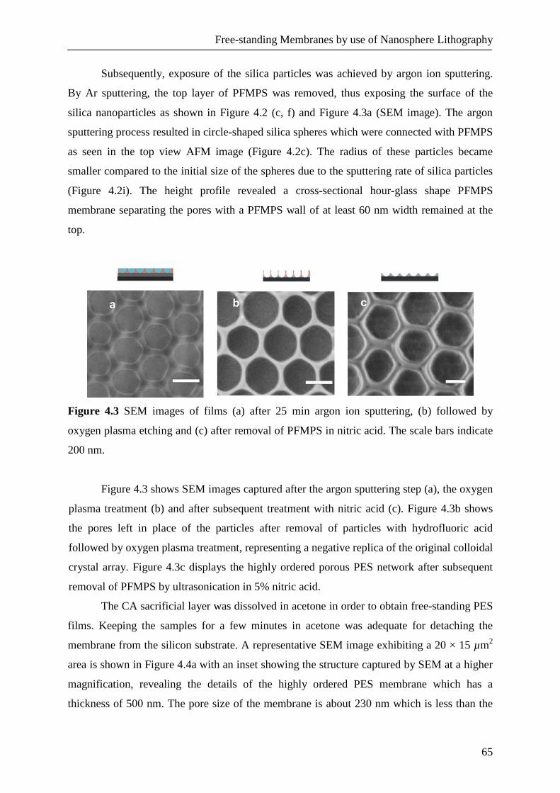
Free-standing Membranes by use of Nanosphere Lithography
65
Subsequently, exposure of the silica particles was achieved by argon ion sputtering.
By Ar sputtering, the top layer of PFMPS was removed, thus exposing the surface of the
silica nanoparticles as shown in Figure 4.2 (c, f) and Figure 4.3a (SEM image). The argon
sputtering process resulted in circle-shaped silica spheres which were connected with PFMPS
as seen in the top view AFM image (Figure 4.2c). The radius of these particles became
smaller compared to the initial size of the spheres due to the sputtering rate of silica particles
(Figure 4.2i). The height profile revealed a cross-sectional hour-glass shape PFMPS
membrane separating the pores with a PFMPS wall of at least 60 nm width remained at the
top.
Figure 4.3 SEM images of films (a) after 25 min argon ion sputtering, (b) followed by
oxygen plasma etching and (c) after removal of PFMPS in nitric acid. The scale bars indicate
200 nm.
Figure 4.3 shows SEM images captured after the argon sputtering step (a), the oxygen
plasma treatment (b) and after subsequent treatment with nitric acid (c). Figure 4.3b shows
the pores left in place of the particles after removal of particles with hydrofluoric acid
followed by oxygen plasma treatment, representing a negative replica of the original colloidal
crystal array. Figure 4.3c displays the highly ordered porous PES network after subsequent
removal of PFMPS by ultrasonication in 5% nitric acid.
The CA sacrificial layer was dissolved in acetone in order to obtain free-standing PES
films. Keeping the samples for a few minutes in acetone was adequate for detaching the
membrane from the silicon substrate. A representative SEM image exhibiting a 20 × 15 µm2
area is shown in Figure 4.4a with an inset showing the structure captured by SEM at a higher
magnification, revealing the details of the highly ordered PES membrane which has a
thickness of 500 nm. The pore size of the membrane is about 230 nm which is less than the

Chapter 4
66
size of the particles used due to the difference in sputtering rate of PFMPS and silica
nanoparticles in a stream of Ar+
ions. With a thickness of 500 nm, the membrane was strong
enough to be peeled off and handled with tweezers. The PES films that peeled off in acetone
were readily transferred onto a substrate without any damage to the membrane (Figure 4.4b
and c), which proved the mechanical stability of the porous films. The lateral dimensions of
the membranes are in principle only limited by the size of the substrate used.
Figure 4.4 (a) SEM images of a PES membrane after removing the sacrificial cellulose
acetate layer in acetone, (b) SEM image of the membrane after being peeled off and
transferred to a substrate (c) optical photograph of a piece of a PES membrane (picked up by
tweezers) after floating off from the substrate.
The pore size can be simply controlled by changing the size of the silica particles
used. We here varied the size of the silica particles to show the fabrication of membranes
with different pore sizes. Figure 4.5 shows SEM images of membranes made from silica
particle sizes of 150 nm, 300 nm and 500 nm. Figure 4.5d shows a membrane fabricated from
a mixture of particles with sizes of 150 nm and 500 nm. Since the voids between the particles
are larger when using a mixture of particles, more material fills the voids which resulted in
wider membrane walls.
Figure 4.5 PES membranes made from (a) 150-nm, (b) 300-nm, (c) 500-nm particles, and (d)
mixed 150-nm and 500-nm particles employing the fabrication sequence in Figure 4.1.
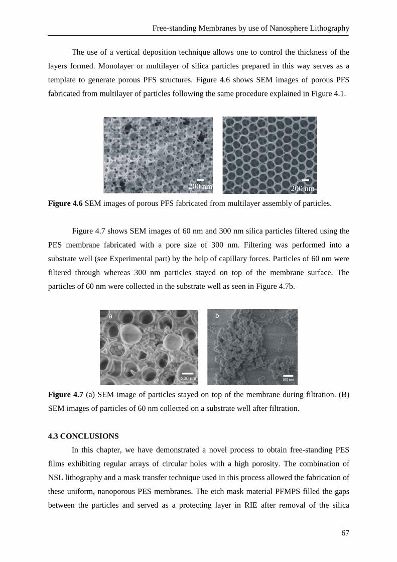
Free-standing Membranes by use of Nanosphere Lithography
67
The use of a vertical deposition technique allows one to control the thickness of the
layers formed. Monolayer or multilayer of silica particles prepared in this way serves as a
template to generate porous PFS structures. Figure 4.6 shows SEM images of porous PFS
fabricated from multilayer of particles following the same procedure explained in Figure 4.1.
Figure 4.6 SEM images of porous PFS fabricated from multilayer assembly of particles.
Figure 4.7 shows SEM images of 60 nm and 300 nm silica particles filtered using the
PES membrane fabricated with a pore size of 300 nm. Filtering was performed into a
substrate well (see Experimental part) by the help of capillary forces. Particles of 60 nm were
filtered through whereas 300 nm particles stayed on top of the membrane surface. The
particles of 60 nm were collected in the substrate well as seen in Figure 4.7b.
Figure 4.7 (a) SEM image of particles stayed on top of the membrane during filtration. (B)
SEM images of particles of 60 nm collected on a substrate well after filtration.
4.3 CONCLUSIONS
In this chapter, we have demonstrated a novel process to obtain free-standing PES
films exhibiting regular arrays of circular holes with a high porosity. The combination of
NSL lithography and a mask transfer technique used in this process allowed the fabrication of
these uniform, nanoporous PES membranes. The etch mask material PFMPS filled the gaps
between the particles and served as a protecting layer in RIE after removal of the silica

Chapter 4
68
spheres. Pores were generated in the PES layer during RIE. Detachment of the PES
membrane from the substrate was achieved by dissolving the sacrificial CA layer in acetone.
A free-standing PES film was obtained, which was used to perform feasibility filtration
experiments. Silica particles were successfully separated by size. Since the size of the silica
particles can be varied, membranes with a range of pore sizes down to 150 nm were
fabricated using this process.
4.4 EXPERIMENTAL
Silica nanoparticles were purchased from Polysciences Inc. (diameter = 300 nm,
standard deviation <10%) as an aqueous suspension, particles of 60 nm were synthesized
following a literature procedure.[34] Polyethersulfone (PES) (UDEL P-1700) was obtained
from Solvay Advanced Polymers and cellulose acetate (CA) was purchased from Acros
Organics. N,N,N',N',-Tetramethylethylenediamine (TMEDA), ferrocene,
dichloromethylphenylsilane, Karstedt’s catalyst and Et3
[1]Methylphenylsilaferrocenophane was prepared as described earlier.[17,26] The
monomer was purified by several crystallization steps from n-heptane at –70 °C followed by
vacuum sublimation. Transition-metal-catalyzed ring opening polymerization was carried out
in the presence of Et3SiH with the addition of Karstedt’s catalyst. The polymer obtained was
precipitated in n-heptane. The weight average and number average molar masses Mw and Mn
of the polymer were determined by gel permeation chromatography (GPC) measurements in
THF, using polystyrene calibration, Mw = 5.5 x 10⁴ g/mol, Mn = 5.1 x 10⁴ g/mol, Mw/Mn =
1.09.
SiH were purchased from Aldrich and
were used as obtained.
Silicon substrates were cleaned by immersion in piranha solution, conc. H2SO4 and
33% H2O2 in a 3:1 volume ratio (Warning! piranha should be handled with caution; it can detonate unexpectedly) for 15 min to form a clean SiO2 layer at the surface. The substrates
were then sonicated in Milli-Q water and ethanol for 1 min, and dried with N2. CA layers of
150 nm were obtained by spin coating in a cleanroom environment from toluene solution.
Subsequently, a PES film of 500 nm was spin-coated from chloroform onto the CA film. The
PES film was exposed to oxygen plasma for 30 sec for mild oxidation in a reactive-ion
eching (O2-RIE) setup, carried out in an Elektrotech PF 340 apparatus (10 mTorr, 20 sccm
O2, 10 W). Mild oxidation of PES resulted in a hydrophilic surface which allowed the
assembly of silica particles. A monolayer of silica colloidal particles on the PES substrate

Free-standing Membranes by use of Nanosphere Lithography
69
was prepared by capillary assisted deposition at a speed of 0.5 µm/s.[33] A layer of 80 nm PFS
was spin-coated onto the particle layer from 2 wt % PFS solution in toluene. The top layer of
PFS was etched away by argon plasma sputtering for 25 min (Ion Beam Etcher, 350 V, 6
mA) resulting in exposure of the top of the silica particles. The silica particles were removed
by dipping the substrate into a 10 wt% aqueous hydrogen fluoride (HF) solution for 12 h,
subsequently rinsing with Milli-Q water and drying with N2
Oxygen plasma etching experiments, for the removal of PES in unprotected areas,
were performed in a reactive-ion etching (O
. (Warning! HF solution should be handled with caution; it can cause serious health problems)
2-RIE) setup, carried out in an Elektrotech PF
340 apparatus (10 mTorr, 20 sccm O2
In order to gauge membrane performance, a simple filtration experiment was carried
out by filtering silica particles with different diameters onto a substrate exhibiting ‘wells’
which were fabricated by Focused Ion Beam (FIB). The wells displayed a depth of 10 µm
and a diameter of 10 µm to provide capillary forces for particles to be filtrated. The PES
membrane was placed on top of the well, and a droplet of an aqueous solution containing a
mixture of 300 nm and 60 nm silica particles was placed on top of the membrane.
, 50 W) for 5 min. The substrate was sonicated with 10
wt% aqueous nitric acid solution in a Branson 8510 ultrasonic bath to remove PFMPS. Free
standing membranes were obtained by dipping the etched substrates in acetone to dissolve the
CA sacrificial layer.
All SEM images were taken with a HR-LEO 1550 FEF SEM. The samples were not
coated with a conducting layer. AFM measurements were carried out with a Dimension
D3100 using a NanoScope IVa controller equipped with a hybrid 153 scanner (Veeco/Digital
Instruments (DI), Santa Barbara, CA) under ambient conditions. Silicon cantilevers from
Nanosensors (Nanosensors, Wetzlar, Germany) were used for intermittent contact (tapping)
mode operation.
4.5 ACKNOWLEDGEMENTS
We thank Mr. Mark Smithers for the SEM images and Mr. Clemens Padberg for the
technical support.

Chapter 4
70
4.6 REFERENCES
[1] L. J. Zeman, A. L. Zyndey, Microfiltration and Ultrafiltration Principles and
Applications, Marcel Dekker Inc., New York 1996.
[2] M. Cheryan, Ultrafiltration and Microfiltration Handbook, Technomic Publishing
Company, Lanchester, PA 1998.
[3] J. Mallevialle, P. E. Odendaal, M. R. Wiesner, Water Treatment Membrane
Processes, McGraw-Hill, New York 1996.
[4] M. Ulbricht, Polymer 2006, 47, 2217.
[5] R. L. Fleischer, P. B. Price, R. M. Walker Nuclear Tracks in Solids. University of
California Press, Berkeley, CA 1975.
[6] R. C. Furneaux, W. R. Rigby, A. P. Davidson, Nature 1989, 337, 147.
[7] C. R. Martin, Science 1994, 266, 1961.
[8] C. Jiang, V. V. Tsukruk, Soft Matter 2005, 1, 334.
[9] G. J. Liu, J. F. Ding, T. Hashimoto, K. Saijo, F. M. Winnik, S. Nigam, Chem. Mater.
1999, 11, 2233.
[10] A. S. Zalusky, R. Olayo-Valles, C. J. Taylor, M. A. Hillmeyer, J. Am. Chem. Soc.
2001, 123, 1519.
[11] S. Y. Chou, MRS Bull. 2001, 26, 512.
[12] D. Zimnitsky, V. V. Shevchenko, V. V. Tsukruk, Langmuir 2008, 24, 5996
[13] B. Gates, Y. Yin, Y. Xia, Chem. Mater. 1999, 11, 2827.
[14] P. Jiang, J. F. Bertone, V.L. Colvin, Science 2001, 291, 453.
[15] X. Chen, Z. Chen, N. Fu, G. Lu, B. Yang, Adv. Mater. 2003, 15, 1413.
[16] U. C. Fischer, H. P. Zingsheim, J. Vac. Sci. Technol. B. 1981, 19, 881.
[17] D. A. Foucher, B. Z. Tang, I. Manners, J. Am. Chem. Soc. 1992, 114, 6246.
[18] I. Manners, Synthetic Metal-Containing Polymer, Wiley-VCH, Weinheim, Germany
2004.
[19] K. Kulbaba, I. Manners, Macromol. Rapid Commun. 2001, 22, 711.
[20] C. Hinderling, Y. Keles, T. Stöckli, H. F. Knapp, T. De Los Arcos, P. Oelhafen, I.
Korczagin, M. A. Hempenius, G. J. Vancso, R. Pugin, H. Heinzelmann, Adv. Mater.
[21]
2004, 16, 876.
J. Q. Lu, T. E. Kopley, N. Moll, D. Roitman, D. Chamberlin, Q. Fu, J. Liu, T. P.
Russell, D. A. Rider, I. Manners, M. A. Winnik, Chem. Mater.
[22] R. G. H. Lammertink, M. A. Hempenius, J. E. Van den Enk, V. Z.-H. Chan, E. L
2005, 17, 2227.
Thomas, G. J. Vancso, Adv. Mater. 2000, 12, 98.

Free-standing Membranes by use of Nanosphere Lithography
71
[23] A. C. Arsenault, H. Míguez, V. Kitaev, G. A. Ozin, I. Manners, Adv. Mater.
[24]
2003, 15, 503.
M. Péter, R. G. H. Lammertink, M. A. Hempenius, G. J. Vancso, Langmuir 2005, 21,
5115.
[25] I. Korczagin,
R. G. H. Lammertink, M. A. Hempenius, S. Golze, G. J. Vancso,
Adv.
[26] I. Korczagin, S. Golze, M. A. Hempenius, G. J.
Polym. Sci. 2006, 200, 91.
3663.
Vancso, Chem. Mater. 2003, 15,
[27] M. A. Hempenius, R. G. H. Lammertink, M. Péter, G. J. Vancso,
Macromol. Symp.
2003, 196
[28] J. Y. Cheng, C. A. Ross, V. Z. H. Chan, E. L. Thomas, R. G. H. Lammertink, G. J.
, 45.
Vancso,
[29] R. G. H. Lammertink, M. A. Hempenius, V. Z. Chan, E. L. Thomas, G. J. Vancso
Adv. Mater. 2001, 13, 1174.
Chem. Mater. 2001, 13, 429.
[30] J. Lu, D. Chamberlin, D. A. Rider, M. Liu, I. Manners, T. P. Russell, Nanotechnology
2006, 17, 5792.
[31] K. Temple, J. A. Massey, Z. H. Chen, N. Vaidya, A. Berenbaum, D. M. Foster, I.
Manners, J. Inorg. Organomet. Polym. 1999, 9, 189.
[32] (a) Z. Fan, Z. Wang, N. Sun, J. Wang, S. Wang, J. Membr. Sci. 2008, 320, 363. (b) D.
S. Wavhal, E. R. Fisher, J. Polym. Sci. Part B: Polym. Phys. 2002, 40, 2473.
[33] X. Y. Ling, L. Malaquin, D. N. Reinhoudt, H. Wolf, J. Huskens, Langmuir 2007, 23,
9990.
[34] X. Y. Ling, D. N. Reinhoudt, J. Huskens, Langmuir 2006, 22, 8777.

Chapter 4
72

Chapter 5
Direct Surface Structuring of Organometallic Resists Using
Nanoimprint Lithography
ABSTRACT. The availability of suitable resist materials is essential for nanoimprint
lithography (NIL). In this chapter, the application of poly(ferrocenylmethylphenylsilane)
(PFMPS) as a new type of imprint resist is reported. As PFMPS contains iron and silicon in
the main chain, it possesses a very high resistance to reactive ion etching. Polymer patterns
formed after imprinting were transferred into silicon substrates owing to the high etch
resistivity of PFMPS. The parameters for imprinting such as polymer molar mass and initial
film thickness were investigated. A decrease in the initial film thickness facilitated the
residual layer removal, as well as the pattern transfer. Only upon complete removal of the
residual layer with argon plasma, pattern transfer resulted in aspect ratios up to 4:1 and lower
surface roughness.
______________________________
This work has been published in C. Acikgoz, M.A. Hempenius, G. J. Vancso, J. Huskens,
Direct surface structuring of organometallic resists using nanoimprint lithography,
Nanotechnology 2009, 20, 135304.

Chapter 5
74
5.1 INTRODUCTION
Imprint lithography[1, 2] has become an enabling platform to fabricate micro and
nanostructures for a wide variety of applications, for example in electronics[3, 4] and in bio-
nanotechnology.[5, 6] Among the imprint-based lithographic techniques, thermal nanoimprint
lithography (NIL)[1, 2] is one of the most versatile methods, capable of fabricating patterns
from less than ten nanometers to a few microns on a large area, at a low cost with a high
throughput. Multiple copies of the pattern can be produced once the stamp is available. A
hard stamp is used to replicate patterns by NIL, distinguishing it from microcontact printing
(µCP), which uses a soft and flexible PDMS stamp. The hard features on NIL molds can
enable imprinting of features with sizes down to below 10 nm, which can not be achieved by
µCP using a soft stamp.[2] In order to create the patterns, a stamp is pressed into a thin layer
of polymer resist, followed by heating at a temperature approximately 80 °C above the glass
transition temperature (Tg) of the polymer. Polymer and stamp are cooled to below the Tg of
the polymer followed by demolding of the stamp, leaving the desired patterns in the polymer
film.[3] Pattern transfer is enabled by anisotropic etching such as reactive ion etching.[7]
This technology has found widespread use, however, the resist material is generally
regarded as one of the challenges of this technique.[8] There are some requirements for
materials to be employed as a NIL resist such as modest imprint temperature and pressure,
proper mold release and etch selectivity.[8] Poly(methyl methacrylate) and polystyrene are
most widely used as NIL resists and they work well in many processes. Nevertheless, they
have in some occasions be subject to mold-sticking and fracture defects during mold
release.[9, 10] High imprint temperatures can also cause thermal stress and degradation in the
polymer film and increase the processing time.[11] The use of imprinted patterns as an etch
mask is necessary if patterns are to be transferred into the substrate using plasma etching.
PMMA breaks down easily when exposed to reactive species in RIE processing, i.e. it does
not show a high etch resistivity in plasma processing, which prevents pattern transfer into
silicon and similar substrates. Anisotropic etching of submicron trenches in silicon has been
achieved by using a non-standard SF6 and C2Cl3F3 plasma with a Si/PMMA etch selectivity
of about 10:1.[12] The fabrication of high-aspect-ratio patterns can be achieved by
implementing an additional metal evaporation and lift-off process, which can increase the
selectivity up to 40:1. This approach, however, introduces additional problems such as
granularity of the metal and concomitant edge roughness.[13]
Poly(ferrocenylsilane) (PFS),[14-18] containing iron and silicon atoms in the main
chain, is a class of organometallic polymers which show very diverse and interesting

Direct Surface Structuring of PFS by NIL
75
properties. PFSs can be prepared by thermal ring-opening polymerization of the
corresponding ferrocenophanes,[15] by anionic polymerization and other types of chemistries.
Pattern transfer into various substrates by using these organometallic homopolymers as inks
in soft lithography owing to their etch resistance has been demonstrated already.[19-21] The
high etch resistance of PFS compared to silicon substrates has enabled the fabrication of
structures with aspect ratios of 10. An etch rate contrast of 600:1 (silicon to PFS) was
established after using PFS as a mask material.[22] In a recent paper, pattern transfer fidelity
in capillary force lithography using PFS plasma etch resists was studied. An optimal viscosity
range was established with respect to molar masses and processing temperatures. In the
optimal processing window polymers possess enough mobility to allow for fast surface
pattern fromation, yet they are not too mobile thus patterns preserve shapes when quenched
to below Tg prior to serving as etch masks.[23]
In this chapter, the use of poly(ferrocenylmethylphenylsilane) (PFMPS) as a NIL
resist is described. As shown earlier,[15] this polymer has a low Tg, it forms homogeneous
films and has a high etch resistivity. In the current study, thermal imprinting of PFMPS is
demonstrated and the patterns are transferred into silicon substrates by applying different
compositions of gases in plasma etching. The residual layer is removed by treatment with
argon plasma sputtering prior to transfer into the substrate. Imprint parameters such as initial
film thickness and polymer molar mass are investigated. Employing PFMPS as an etch mask
reduces the number of process steps by eliminating the need for metal evaporation and lift-
off, which implies faster and easier fabrication of nanostructured surfaces.
5.2 RESULTS & DISCUSSION
5.2.1 Synthesis and Characterization of Poly(ferrocenylmethylphenylsilane)
Poly(ferrocenylmethylphenylsilane) (PFMPS) is an amorphous polymer due to atactic
substitution on the silicon atom in the main chain, and has a glass transition temperature
suitable for thermal imprinting. Since crystallization may destruct patterns, it was essential to
choose a non-crystalline polymer. PFMPS forms homogeneous films and has a Tg above
room temperature which is important to preserve the shape of the structures after removal of
the stamp. The extrapolated value of the Tg for PFMPS to infinite molecular weight was
reported to be 92 oC.[19] The synthesis and characterization of PFMPS were carried out
according to a literature procedure (Figure 5.1).[14, 24]
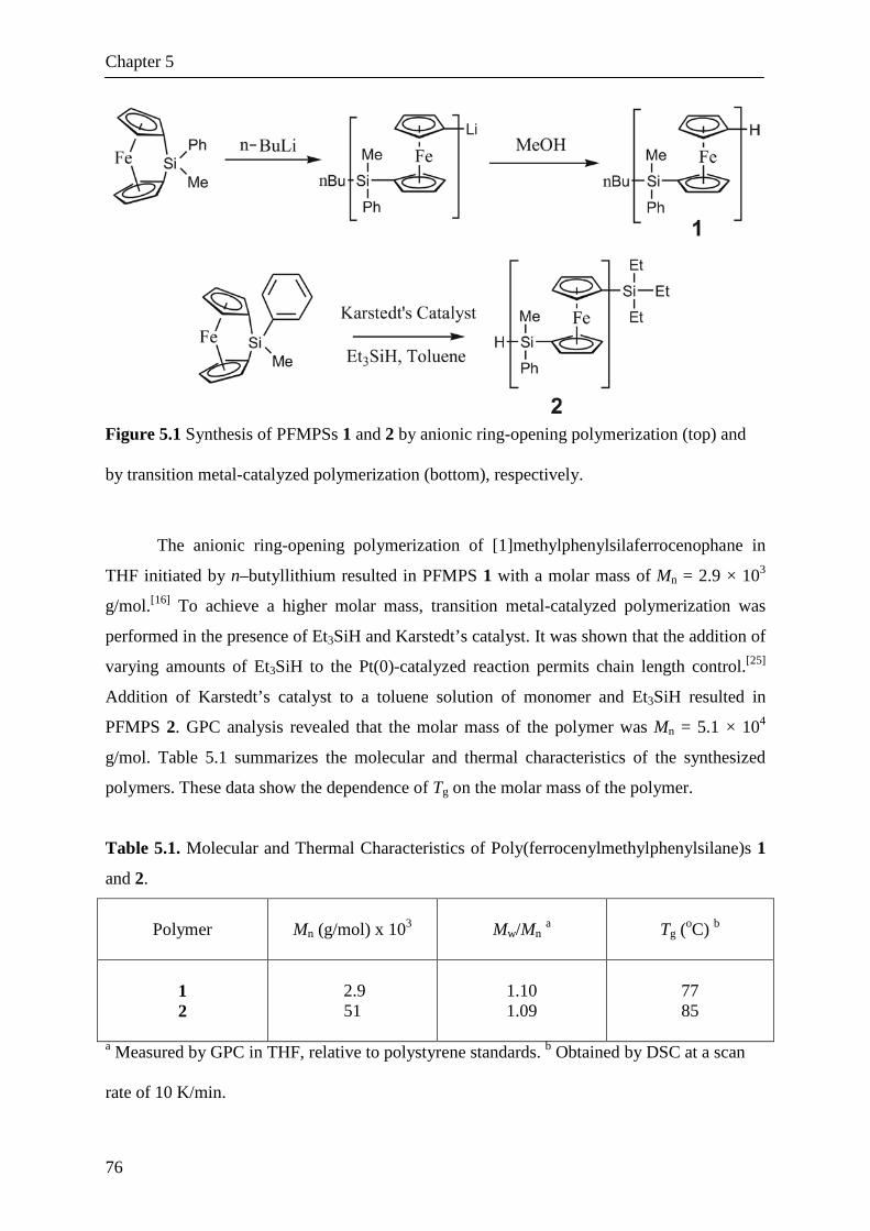
Chapter 5
76
Figure 5.1 Synthesis of PFMPSs 1 and 2 by anionic ring-opening polymerization (top) and
by transition metal-catalyzed polymerization (bottom), respectively.
The anionic ring-opening polymerization of [1]methylphenylsilaferrocenophane in
THF initiated by n–butyllithium resulted in PFMPS 1 with a molar mass of Mn = 2.9 × 10³
g/mol.[16] To achieve a higher molar mass, transition metal-catalyzed polymerization was
performed in the presence of Et3SiH and Karstedt’s catalyst. It was shown that the addition of
varying amounts of Et3SiH to the Pt(0)-catalyzed reaction permits chain length control.[25]
Addition of Karstedt’s catalyst to a toluene solution of monomer and Et3SiH resulted in
PFMPS 2. GPC analysis revealed that the molar mass of the polymer was Mn = 5.1 × 10⁴
g/mol. Table 5.1 summarizes the molecular and thermal characteristics of the synthesized
polymers. These data show the dependence of Tg on the molar mass of the polymer.
Table 5.1. Molecular and Thermal Characteristics of Poly(ferrocenylmethylphenylsilane)s 1
and 2.
Polymer
Mn (g/mol) x 103
Mw/Mn a
Tg (oC) b
1 2
2.9 51
1.10 1.09
77 85
a Measured by GPC in THF, relative to polystyrene standards. b Obtained by DSC at a scan
rate of 10 K/min.

Direct Surface Structuring of PFS by NIL
77
5.2.2 Thermal Nanoimprinting of PFMPS
PFMPS 1 and 2, having different molar masses, were used as resists in NIL. Thin
polymer films were spin-coated on silicon oxide substrates from toluene solutions, followed
by softbaking at 120 oC to evaporate the remaining solvent and to improve the resist-substrate
adhesion. By the spin-coating process, it was possible to control the thickness of the polymer
layer and to prepare uniformly coated silicon substrates.[26] The resulting polymer films were
homogeneous, which is essential for imprinting. Following spin-coating, the sample and the
stamp were heated to 150 ºC and pressure of 80 bar was applied.
In the case of the low molar mass PFMPS 1, the stamp features were transferred into
the polymer, but incomplete filling and dewetting were observed (Figure 5.2a). These
problems are attributed to the low molar mass of the polymer, which favors dewetting. In
contrast, in the case of the high molar mass polymer 2, no dewetting was observed. Figure 5.2
(b and c) shows imprinted lines with a width of 1 µm and a 5 µm period and of 100 nm wide
lines with a 1 µm period, respectively, imprinted into 120 nm of PFMPS 2 at a temperature
of 150 °C at 80 bar for 1 min. The features of the stamps were successfully transferred into
PFMPS 2 after demolding at a temperature of 75 ºC. Therefore, all subsequent experiments
were performed with PFMPS 2.
Figure 5.2 (a) Optical micrograph of imprint into PFMPS 1. (b) AFM image of imprinted
lines with a width of 1 µm and a 5 µm period and (c) SEM image of imprinted lines of 200
nm wide with a 500 nm period obtained after NIL in PFMPS 2.

Chapter 5
78
The flow behavior of polymers at elevated temperatures is a crucial issue in NIL.
Polymers at temperatures above their glass transition temperature are liquids, but with a very
high viscosity. As the temperature increases, the viscosity of polymer decreases and the
mobility of flow increases. Therefore, the viscosity of PFMPS 2 was determined. Viscosity
measurements were performed in a parallel plate configuration using oscillatory shear flow
experiments at different temperatures. At every measurement point, viscosity was calculated
as a ratio of shear stress and shear rate. The zero-shear-rate viscosity was determined by
extrapolation of the viscosity values as a function of shear rate. The zero-shear-rate viscosity
of PFMPS 2 was found to be 334 Pa.s at 150 °C (the imprint temperature), which is
appropriate for NIL since good-quality patterns can typically be generated with polymers
having viscosities in the range of 50 to 1500 Pa.s.[23]
Thermal NIL typically results in the formation of a residual resist layer in the
imprinted regions. The thickness and the uniformity of the residual layer is thus critical as an
additional etching step is required to remove this residual layer before the patterns can be
transferred to the substrate. Oxygen and oxygen-containing plasmas are most commonly
employed to remove a residual layer. The imprinted PFMPS 2 films were exposed to oxygen
reactive ion etching (O2-RIE) in order to remove the residual layer.
Figure 5.3a demonstrates the influence of oxide layer formation upon oxygen plasma
treatment of PFMPS. The residual layer was not removed by this process while the roughness
(compared to Figure 5.2b) became more pronounced. This was confirmed by AFM roughness
measurements which showed that the roughness before oxygen plasma treatment was 1.0 nm
whereas it increased to 3.4 nm after O2 plasma. Upon exposure to oxygen plasma, a Si/Fe
oxide layer is formed at the surface of PFMPS since inorganic components are converted into
nonvolatile oxides as witnessed by earlier.[27] After addition of CHF3 gas to the plasma, the
residual polymer layer was removed. This was confirmed by the observation that further
etching into the silicon substrate, which was achieved by an O2/SF6 plasma and led to an
increased feature height of ~ 400 nm (Figure 5.3b). However, considerable roughness was
still observed in the regions between the lines (Figure 5.3b and c). This roughness is
attributed to traces of residual PFMPS, which, when converted into Si/Fe oxide, acts as an
etch barrier.

Direct Surface Structuring of PFS by NIL
79
Figure 5.3 (a) AFM height image of a thermal imprint into PFMPS 2 upon exposure to
oxygen plasma. AFM height (b) and phase (c) images acquired after residual layer removal
by O2 and CHF3 plasma followed by etching into the substrate by applying an O2/SF6 plasma.
In conclusion, upon treatment of PFMPS resist with oxygen plasma, coverage of the
whole surface with an oxide layer hindered the removal of the residual layer. A proper
selection of gases from which the plasma is generated could decrease the formation of this
oxide layer and thus enhance etching. However, the surface became rough during the initial
steps of etching, and this roughness was transferred to the substrate after applying SF6 and O2
plasma (Figure 5.3c). Therefore, this oxide layer between the lines limits the etch contrast
and prevents the fabrication of high-aspect-ratio patterns.
Optimization of the RIE process conditions requires quantification and control of the
residual layer thickness. Achieving a minimal residual layer thickness is advantageous for
most imprint applications as this minimizes loss of dimensional accuracy during the plasma
etching process. By tuning the initial film thickness, we tried to obtain a thin residual layer.
Polymer 2 was spin-coated onto a silicon surface to thicknesses of 120, 70 and 40 nm,
respectively. The thickness of the residual layer after imprinting was around 80 nm for the
120 nm initial film thickness, as was measured by AFM after scratching. After decreasing the
initial thickness of the polymer layer to 70 nm, the thickness of the residual layer was
determined to be 50 nm.

Chapter 5
80
The cross-section SEM images given in Figure 5.4 show the residual layer
thicknesses. When the initial film thickness was 70 nm, the thickness of the residual layer
was found to be 40 to 50 nm (Figure 5.4a) Decreasing the initial film thickness to 40 nm
resulted in a residual layer of 20 to 30 nm as seen in Figure 5.4b. When calculating the
residual layer thickness from the observed, partially filled, feature heights, similar values are
obtained: the height of 300 nm observed for the 100 nm wide lines at 1 μm period (Figure
5.4a) corresponds to a residual layer of 45 nm, while the height of 140 nm observed for 1 µm
lines at 5 µm period (Figure 5.4b) corresponds to a residual layer thickness of about 20 nm.
Figure 5.4 Cross-section SEM images of structures imprinted into (a) 70 nm and (b) 40 nm
initial layer thickness of PFMPS 2.
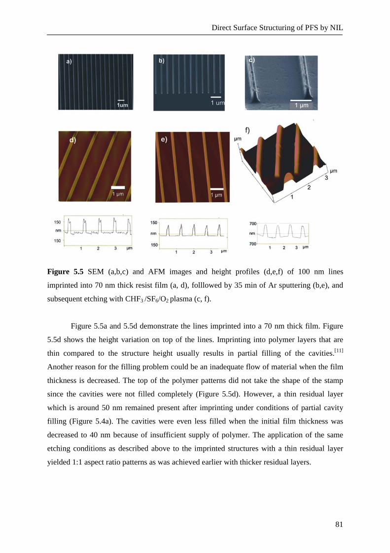
Direct Surface Structuring of PFS by NIL
81
Figure 5.5 SEM (a,b,c) and AFM images and height profiles (d,e,f) of 100 nm lines
imprinted into 70 nm thick resist film (a, d), folllowed by 35 min of Ar sputtering (b,e), and
subsequent etching with CHF3 /SF6/O2 plasma (c, f).
Figure 5.5a and 5.5d demonstrate the lines imprinted into a 70 nm thick film. Figure
5.5d shows the height variation on top of the lines. Imprinting into polymer layers that are
thin compared to the structure height usually results in partial filling of the cavities.[11]
Another reason for the filling problem could be an inadequate flow of material when the film
thickness is decreased. The top of the polymer patterns did not take the shape of the stamp
since the cavities were not filled completely (Figure 5.5d). However, a thin residual layer
which is around 50 nm remained present after imprinting under conditions of partial cavity
filling (Figure 5.4a). The cavities were even less filled when the initial film thickness was
decreased to 40 nm because of insufficient supply of polymer. The application of the same
etching conditions as described above to the imprinted structures with a thin residual layer
yielded 1:1 aspect ratio patterns as was achieved earlier with thicker residual layers.

Chapter 5
82
5.2.3 Pattern Transfer into the Silicon Substrate
Figure 5.6 Etching process applied to completely remove the residual layer and to etch into
the substrate.
Figure 5.6 illustrates the procedure applied to eliminate the residual layer problem.
RIE is a combination of chemical and physical etching.[28] The formation of a nonvolatile
oxide layer at the surface of PFMPS is due to chemical etching. Physical etching becomes
less pronounced during RIE since the oxide layer acts as a very strong mask preventing
further etching into the substrate. Argon sputtering, which is a purely physical etching
process, is expected to prevent the formation of nonvolatile oxide since the layer is physically
bombarded with high energy ions and is removed by the corresponding sputtering effect.
Therefore, physical etching was performed with sputtering using high energy Ar ions to
remove the residual layer. The etch rate of PFMPS 2 was determined to be 1.5 nm/min after
exposure to argon plasma. Taking into account this value, the imprinted sample was exposed
to argon plasma for 35 min to ensure that the residual layer was removed completely.
The height difference before (Figure 5.5a, d) and after Ar plasma (Figure 5.5b, e)
treatment revealed the complete removal of PFMPS in the recessed regions. Exposure of
PFMPS to Ar plasma resulted in a high initial roughness (data not shown). This roughness
was not observed after complete removal of PFMPS from recessed regions by sputtering as
can be seen in Figure 5.5e. Keeping the film thickness as thin as possible significantly
reduces the required time of treatment with Ar plasma. Further etching into the substrate also
proved that no residual layer remained (Figure 5.5c, f). Reactive ion etching with a mixture of
CHF3 (20 sccm), O2 (20 sccm) and SF6 (50 sccm) was performed to transfer these lines into
the substrate[29] (Figure 5.5c). An aspect ratio of 4:1 was achieved after a 2 min treatment
with the plasma containing these gases. Using this process we obtained etch rates of 400
nm/min into Si and around 1 nm/min in PFMPS layer resulting in an etch rate contrast of
approximately 400. The height profile in Figure 5.5f shows that the sidewalls are not
completely vertical after etching into the substrate.
It was observed that changes in pattern size influenced the etching characteristics of
the patterns. More vertical sidewalls were obtained for 1 µm wide lines (Figure 5.7a). The

Direct Surface Structuring of PFS by NIL
83
roughness on the recessed regions was also diminished after Ar plasma, which facilitated
etching into the substrate. Defect-free patterns were thus reproducibly obtained over large
areas (Figure 5.7b).
Figure 5.7 (a) SEM image of sidewalls obtained after etching into the substrate for 1 µm
wide lines. (b) Large area SEM image of etched sample with a CHF3 /SF6/O2 plasma.
5.3 CONCLUSIONS
We have described the application of PFMPS as a resist in nanoimprint lithography. Stable,
homogeneous high molar mass PFMPS films obtained by spin coating were imprinted and
the resulting patterns were further transferred into the substrate by reactive ion etching.
Decreasing the initial film thickness and tuning the reactive ion etching conditions facilitated
the residual layer removal and improved the pattern transfer. In order to obtain high aspect
ratios, the residual layer was completely removed by Ar sputtering since direct etching
without removal of the residual layer gave rise to oxide layer formation, which prevented
further pattern transfer. A drawback of this process is the relatively long sputtering time
needed. This can be further improved by (i) increase of the sputter rate, (ii) further reduction
of the residual layer, and/or (iii) use of processes that circumvent the formation of a residual
layer altogether.[30] Overall, it was shown that PFMPS, because of its excellent etch contrast
vs Si, can be used as a single step resist since there is no need for metal lift-off, which renders
this approach a low-cost and potentially high-throughput process
5. 4 EXPERIMENTAL
5.4.1 Polymer Synthesis and Characterization
N,N,N',N',-Tetramethylethylenediamine (TMEDA), ferrocene, dichloromethylphenyl-
silane, Karstedt’s catalyst, Et3SiH and n-butyllithium were purchased from Aldrich.

Chapter 5
84
[1]Methylphenylsilaferrocenophane was prepared as described earlier.[15, 24] This monomer
was purified by several crystallizations from n-heptane at –70 °C followed by vacuum
sublimation. Polymerizations were carried out in THF in a glovebox purged with prepurified
nitrogen. n-Butyllithium was used as initiator for anionic polymerization and the reaction was
terminated after 2 h by adding a few drops of degassed methanol. The polymer was
precipitated in methanol and dried. Transition metal-catalyzed ring opening polymerization
of [1]methylphenylsilaferrocenophane was carried out in the presence of Et3SiH with the
addition of Karstedt’s catalyst. The polymer was then precipitated in n-heptane. For resists
with low/moderate molar masses, anionic polymerisation was employed, while higher molar
masses were achieved using transition metal-catalyzed polymerisation. Molar mass
characteristics of the polymer were determined by gel permeation chromatography (GPC)
measurements in THF, using polystyrene calibration. A Perkin-Elmer Pyris 1 differential
scanning calorimeter was used for the determination of glass transition temperatures (Tg) at a
scan rate of 10 K/min.
Viscosity measurements were performed on a Physica UDS 200 rheometer using a parallel
plate configuration. The gap between the plates was 0.5 mm and a shear strain of 1 % was
applied. The viscosity was measured at frequencies from 0.01 to 50 Hz as a function of
temperature between 80 ºC and 150 ºC. Zero-shear-rate viscosity was calculated by
extrapolation of the viscosity values using an exponential function model for an isothermal
scan at 150 ºC.
5.4.2 Pattern Fabrication
The Si stamp was fabricated by electron beam lithography followed by reactive ion
etching. The stamp has dimensions of 2×2 cm2 and contains 80×40 μm 2 patterned regions
with features of 1 μm lines at 5 μm period, 500 nm lines at 5 μm period, 200 nm lines at 1 μm
period, 200 nm lines at 500 nm spacings, 100 nm lines at 1 μm period, and all at a height of
500 nm. 1H,1H,2H,2H-Perfluorodecyltrichlorosilane was used as an anti-adhesion layer to
facilitate demolding. Cleaning of the substrates and coating of the films were carried out in a
cleanroom. Film thicknesses of 120, 70, and 40 nm were applied, as measured by
ellipsometry. Stamp and substrate were put in contact and a pressure of 80 bar was applied at
a temperature of 150 oC using a hydraulic press (Specac).
After imprinting, the residual layer was removed by argon plasma sputtering applied
for 35 min (Ion Beam Etcher, 350 V, 6 mA). Further etching into the substrate was
accomplished by RIE performed in an Elektrotech PF 340 apparatus. During oxygen plasma
RIE, the pressure inside the etching chamber was 10 mTorr, the substrate temperature was 10
Direct Surface Structuring of PFS by NIL
85
oC and an oxygen flow rate of 20 sccm was maintained. The second etch step was performed
with a mixture of 50% CHF3 and 50% O2 at a pressure of 8 mTorr, with a substrate
temperature of 10 oC. The power was kept at 50 V. The final etch step was enabled with a
mixture of 20 sccm of CHF3 and 20 sccm of O2 and 50 sccm of SF6 at a pressure of 10 mTorr.
The resist was stripped following sonication for 1 h in 10% nitric acid solution. AFM analysis
were carried out with a Nanoscope III multimode AFM (Veeco Co., Santa Barbara, CA) by
using a J scanner. SEM characterization was done with a HR-LEO 1550 FEF SEM. A FEI
Focus Ion Beam apparatus was used to generate the cross sections in order to determine the
exact residual layer thickness.
5.5 ACKNOWLEDGEMENTS
We thank the EC-funded project NAPA that provided the stamp and Mark Smithers
for the SEM images.
5. 6 REFERENCES
[1] S. Y. Chou, P. R. Krauss, P. J. Renstrom, Appl. Phys. Lett. 1995, 67, 3114.
[2] L. J. Guo, J. Phys. D: Appl. Phys. 2004, 37, R123.
[3] M. Beck, F. Persson, P. Carlberg, M. Graczyk, I. Maximov, T. G. I. Ling, L.
Montelius, Microelectron. Eng. 2004, 73-4, 837.
[4] S. Y. Chou, P. R. Krauss, W. Zhang, L. J. Guo, L. Zhuang, J. Vac. Sci. Technol. B
1997, 15, 2897.
[5] F. Johansson, P. Carlberg, N. Danielsen, L. Montelius, M. Kanje, Biomaterials 2006,
27, 1251.
[6] V. N. Truskett, M. P. C. Watts, Trends Biotechnol. 2006, 24, 312.
[7] S. Y. Chou, P. R. Krauss, P. J. Renstrom, Science 1996, 272, 85.
[8] P. Choi, P. F. Fu, L. J. Guo, Adv. Funct. Mater. 2007, 17, 65.
[9] M. D. Chen Y, Boyd E, Moran D, Thayne I, Thomas S J. Vac. Sci. Technol. B 2002,
20, 2887.
[10] Y. Hirai, S. Yoshida, N. Takagi, J. Vac. Sci. Technol. B 2003, 21, 2765.
[11] K. Pfeiffer, F. Reuther, M. Fink, G. Gruetzner, P. Carlberg, I. Maximov, L.
Montelius, J. Seekamp, S. Zankovych, C. M. Sotomayor-Torres, H. Schulz, H. C.
Scheer, Microelectron. Eng. 2003, 67-8, 266.
[12] V. A. Yunkin, D. Fischer, E. Voges, Microelectron. Eng. 1995, 27, 463.
Chapter 5
86
[13] N. Bogdanski, M. Wissen, S. Mollenbeck, H. C. Scheer, J. Vac. Sci. Technol. B 2006,
24, 2998.
[14] D. Foucher, R. Ziembinski, R. Petersen, J. Pudelski, M. Edwards, Y. Z. Ni, J. Massey,
C. R. Jaeger, G. J. Vancso, I. Manners, Macromolecules 1994, 27, 3992.
[15] D. A. Foucher, B. Z. Tang, I. Manners, J. Am. Chem. Soc. 1992, 114, 6246.
[16] R. Rulkens, Y. Z. Ni, I. Manners, J. Am. Chem. Soc. 1994, 116, 12121.
[17] K. Kulbaba, I. Manners, Macromol. Rapid Commun. 2001, 22, 711.
[18] I. Manners, Synthetic Metal-Containing Polymers Wiley-VCH, Weinheim, Germany,
2004.
[19] I. Korczagin, S. Golze, M. A. Hempenius, G. J. Vancso, Chem. Mater. 2003, 15,
3663.
[20] M. A. Hempenius, R. G. H. Lammertink, M. Peter, G. J. Vancso, Macromol. Symp.
2003, 196, 45.
[21] J. Y. Cheng, C. A. Ross, E. L. Thomas, H. I. Smith, G. J. Vancso, Adv. Mater. 2003,
15, 1599.
[22] G. J. Vancso, S. Golze, M. A. Hempenius, H. Hillborg, I. Korczagin, R. G. H.
Lammertink, Polym. Prep. 2003, 44, 197.
[23] I. Korczagin, H. Xu, M. A. Hempenius, G. J. Vancso, Eur. Polym. J. 2008, 44, 2523.
[24] K. Temple, J. A. Massey, Z. H. Chen, N. Vaidya, A. Berenbaum, M. D. Foster, I.
Manners, J. Inorg. Organomet. Polym. 1999, 9, 189.
[25] K. Temple, F. Jakle, J. B. Sheridan, I. Manners, J. Am. Chem. Soc. 2001, 123, 1355.
[26] C. B. Walsh, E. I. Franses, Thin Solid Films 2003, 429, 71.
[27] R. G. H. Lammertink, M. A. Hempenius, V. Z. H. Chan, E. L. Thomas, G. J. Vancso,
Chem. Mater. 2001, 13, 429.
[28] D. M. Manos, D. L. Flamm, Plasma Etching, An Introduction Academic Press, San
Diego, 1988.
[29] H. Jansen, M. de Boer, J. Burger, R. Legtenberg, M. Elwenspoek, Microelectron.
Eng. 1995, 27, 475.
[30] Y. S. Chou, Q. Xia, Nature Nanotechnol. 2008, 3, 295.

Chapter 6
Nanoscale Patterning by UV Nanoimprint lithography Using an
Organometallic Resist
ABSTRACT. This chapter presents the fabrication of poly(ferrocenylmethylphenylsilane)
(PFMPS) patterns by step-and-flash imprint lithography for use as high-contrast etch masks
in dry etch processes. PFMPS was spin-coated onto a resist template made by UV
nanoimprint lithography to create a reactive ion etch resist layer with a thickness variation
corresponding to the imprinted pattern. Etching back the excess of PFMPS by argon
sputtering revealed the imprinted organic resist material, which was subsequently removed by
oxygen plasma. PFMPS lines down to 30 nm were obtained after removal of organic resist by
oxygen plasma. Because PFMPS contains iron and silicon atoms in its main chain, it
possesses a high resistance to oxygen reactive ion etching and e.g., CHF3/O2 or SF6/O2
reactive ion etch processes. PFMPS patterns formed after imprinting were subsequently
transferred into the underlying silicon substrate, and etch rates of 300 nm/min into Si and
around 1 nm/min into the PFMPS layer were achieved, resulting in an etch contrast of
approximately 300.
___________________________
This work has been published in C. Acikgoz, B. Vratzov, M. A. Hempenius, G. J. Vancso, J.
Huskens, Nanoscale Patterning by UV Nanoimprint lithography Using an Organometallic
Resist in ACS Appl. Mater. Inter. 2009, 1, 2645.

Chapter 6
88
6.1 INTRODUCTION
Nanoimprint lithography (NIL) is an emerging nanopatterning technology that allows
the fabrication of nanostructures with high resolution and complements an alternative to
traditional photolithography. Among the imprint-based lithographic technologies, thermal
NIL[1, 2] and UV-light-assisted NIL (UV-NIL)[3, 4] are the two techniques capable of
replicating sub-10-nm features in a low-cost and high-throughput manner. The basic principle
of these imprint-based techniques is that a rigid template or mold with prefabricated
topographic features is used to replicate patterns within a resist layer, which can be
subsequently employed as an etch mask for further pattern transfer. In thermal NIL, mold
patterns are replicated into a thermoplastic material by heating the polymer above its glass
transition temperature and applying pressure on the mold. The necessary but time-consuming
temperature cycling gives rise to differences in the thermal expansion of resist, substrate, and
template, leading to decreased throughput and improper overlay of the device layers and
features.[5] UV-NIL differs from thermal NIL as it is performed at room temperature and low
pressure using low-viscosity, photocurable resists and a transparent, rigid template.[6]
The major components of UV imprint resist materials are an organic acrylate, a cross-
linker, and a photoinitiator. The resist may function as an etch mask for pattern transfer into
the underlying substrate material.
This
method does not require temperature cycling, leading to higher throughput than that in
thermal NIL, and the transparency of the template offers the possibility for easy optical and
high-precision alignment. UV-NIL uses a low-viscosity resist, which also beneficially
influences the imprint force and compression time.
[7] The availability of an appropriate UV-curing resist
material is an important issue because the material has to fulfill several requirements such as
low viscosity, low adhesion to the mold, good adhesion to the substrate, fast curing times,
and high etch resistance to allow pattern transfer into the substrate.[8] There are some
commercially available UV-curable imprinting materials but their characteristics and
properties are still under study.[9]
Poly(ferrocenylsilane)s (PFSs),
The development of new resist materials for UV-NIL,
therefore, remains crucial for enhancing the performance and scope of the technique.
[10-12] containing iron and silicon atoms in the main
chain, show very diverse and interesting properties. PFSs can be prepared by thermal ring-
opening polymerization (ROP) of the corresponding silicon-bridged ferrocenophanes,[13] by
transition-metal-catalyzed ROP[14] and also by anionic polymerization.[15] Especially the latter
technique allows one to produce PFS homopolymers with controlled molar mass and low
polydispersities. In addition, because of the living character of this polymerization, well-

Nanoscale Patterning by UV-NIL
89
defined PFS containing block copolymers can be obtained with regular anionically
polymerizable blocks such as polystyrene, polyisoprene, and many others.[16, 17] Because of
the presence of iron and silicon atoms in the main chain, PFSs show a very high resistance to
reactive ion etching (RIE).[18, 19] Oxygen plasma treatments lead to the formation of iron-
silicon oxide layer domains in PFS-covered areas, which prevents further removal of PFS in
oxygen RIE, while the high resistance to fluorocarbon and SF6 RIE allows pattern transfer
into silicon, silicon oxide, and silicon nitride substrates.
Methods for PFS-based lithography where generated patterns were transferred into
various substrates include soft lithography, involving the use of PFS homopolymers as
inks,
[20]
[21, 22] and block copolymer lithography where self-assembly of hybrid organic-
organometallic block copolymers followed by etching led to nanoperiodic structures with
feature sizes down to 20 nm in silicon substrates[20] and even in thin metal films.[23] The use
of poly(ferrocenylmethylphenylsilane) (PFMPS) as a thermal NIL resist was recently
demonstrated by us.[24] Polymer patterns formed after thermal imprinting were directly
transferred into silicon substrates.
In this chapter, patterns of PFMPS were created on a template made by step-and-flash
imprint lithography (SFIL) using a UV-curable resist.
In order to obtain high aspect ratios, the residual layer was
completely removed by argon sputtering because direct etching without removal of the
residual layer gave rise to oxide layer formation, which prevented further pattern transfer.
Although the direct thermal imprinting process into PFMPS enabled us to transfer the
patterns into the substrate, shortcomings were observed when the feature sizes became
smaller. Small features below 100 nm were not transferred faithfully into the substrate
because they were damaged during argon sputtering. Additional benefits of UV-NIL such as
higher throughput and elimination of thermal cycling, as discussed above, make the
development of a UV-NIL process based on PFSs desirable.
[25] This approach is an example of a
bilayer-type SFIL process because two different materials are used with different etch
selectivities[26] and PFMPS is used as the top resist. The choice of the top resist is critical for
successful dry etching into silicon substrates because the masking layer that is to be etched
should have a distinctly different etch selectivity over the underlying UV-curable resist. After
patterning of the UV-curable resist, PFMPS is spin-coated onto the imprinted structures to
form bilayer structures and subsequent treatment with argon and oxygen plasma provides
patterns of PFMPS with good reproducibility because of the high etch contrast between the
two polymers. The process prevents the formation of a residual layer of PFMPS and thus its
cumbersome removal,[24] which thus constitutes an advantage over the direct hot embossing

Chapter 6
90
of PFMPS. The technique allows the possibility of creating etch-resistant patterns of PFMPS
with sizes down to the nanometer range. Moreover, using PFMPS in this process allows
control of the critical dimensions. Because it is a bilayer process, the final pattern size is not
defined by imprinting alone but also by subsequent etch processes, which makes the role of
PFMPS highly important. It provides a very high selectivity over UV-curable resist due to its
high iron and silicon content which is difficult to obtain with other imprint materials.
6.2 RESULTS & DISCUSSION
Poly(ferrocenylmethylphenylsilane) (PFMPS) was chosen as a resist, because it is an
amorphous polymer due to the unsymmetric substitution on the silicon atom in the main
chain. The use of an amorphous polymer is essential since crystallization may destroy the
imprinted patterns. Also, PFMPS forms homogeneous films. Figure 6.1 summarizes the
bilayer-type SFIL process which consists of the fabrication of patterns of a UV-curable
monomer, deposition of PFMPS on this template, and the etch sequence steps for transferring
the patterns into the substrate. The imprint material was dispensed onto the transfer layer-
coated substrates and the template was brought into contact with the still liquid imprint
material. The transfer layer provided a good adhesion of the imprint material to the substrate.
After exposure and curing of the imprint material, the template was demolded from the
substrate, leaving its negative 3D image. The PFMPS was spin coated on top of the imprinted
structures, creating an organometallic layer with a corresponding thickness variation. Argon
plasma treatment was performed to homogeneously etch down the polymer in order to expose
the organic imprint material. Subsequent treatment with oxygen plasma led to removal of the
exposed organic imprint material and the PFMPS lines were transferred into the substrate,
leading to pattern inversion.

Nanoscale Patterning by UV-NIL
91
Figure 6.1 Fabrication process for creating PFMPS RIE resist patterns and subsequent
pattern transfer into the underlying substrate.
The S-FILTM method[25]
used to create patterns on a substrate, consisting of lines of
100 nm wide with pitches of 1:1, 1:2 and 1:3 and with a height of 100 nm, is shown in Figure
6.2. Figure 6.3 shows a cross-section image of the imprinted lines after spin-coating PFMPS
onto the imprinted structures. As seen in the cross section SEM image in Figure 6.3, the
thickness of the transfer layer was 60 nm and the residual UV-curable resist layer after
imprinting was about 40-50 nm. The dispensing conditions were optimized to obtain such
thin residual layers after imprinting. Since the dispensed monomer was crosslinked upon UV-
curing, spin coating of a solution of PFMPS in toluene did not affect the resist patterns. The
thickness of the PFMPS polymer between the resist lines after spin-coating was determined
to be 120 nm, while on top of the UV-imprinted structures it was about 60 nm. It is crucial to
adjust the layer thickness to planarize the features. The PFMPS thickness applied here
appeared to be sufficient for covering the nanometer and micrometer features completely
with sufficient planarization (see also Figure 6.4, below). The PFMPS provided good wetting
and adhesion performance to the imprint material which is important for subsequent
processing.

Chapter 6
92
Figure 6.2 SEM images of UV-imprinted structures of (a) lines of 100 nm wide with pitches
of 1:1, 1:2 and 1:3 and with a height of 100 nm (b) lines of 100 nm height showing the total
thickness of the residual UV-curable resist layer and the transfer layer.
Figure 6.3 SEM image of a PFMPS layer spin coated on top of imprinted resist lines.
The PFMPS layer was etched back homogeneously in an argon plasma to reveal the
top of the imprinted structures (Figure 6.4). The etch rate of PFMPS upon argon sputtering
was determined to be 1.5 nm min-1. Taking this etch rate into consideration, the time of the
argon sputtering treatment was varied from 15 to 25 min. A time of 15 min proved to be
insufficient for exposing the resist lines (Figure 6.4a), whereas after 25 min the PFMPS layer
was removed, while the resist line shapes were not affected adversely (Figure 6.4b, c).
Opening of the imprinted areas could only be achieved by argon sputtering since oxygen
plasma results in highly etch resistant oxide formation, as mentioned before.[24]

Nanoscale Patterning by UV-NIL
93
Figure 6.4 SEM images of PFMPS structures after argon plasma treatment to expose the
imprinted lines (a) for 15 min, and (b, c) for 25 min. Prior to argon sputtering, PFMPS was
spin coated on top of the UV-imprinted resist lines.
The argon sputtering step was followed by O2 RIE during which the exposed organic
imprint layer and the transfer layer material underneath were selectively etched through.
During this treatment, the PFMPS was oxidized to form a hard Fe/Si oxide layer which
allowed further pattern transfer into the substrate.[18] The O2 RIE etch rates of PFMPS and the
organic imprint material were found to be 1 and 60 nm/min, respectively, which results in an
etch selectivity of 60. Two minutes of treatment with oxygen plasma was sufficient to
remove the imprint material down to the substrate as shown in Figures 6.5a and 6.5b for
features of 80 and 30 nm lines, respectively. PFMPS lines down to 30 nm were obtained after
oxygen plasma treatment as shown in Figure 6.5b. The PFMPS lines revealed a linewidth
roughness of about 5 nm (for the thinner lines, Figure 6.5b), which is similar to the edge
roughness of the lines on the template used during imprinting. The imprint and sputtering
processes apparently did not add additional linewidth roughness to the PFMPS features.
Figure 6.5 SEM images of lines fabricated after O2 RIE of (a) 80 nm PFMPS lines and (b) 30
nm PFMPS lines after 2 min of treatment. (c) 100 nm PFMPS lines after a 2.5 min treatment.
Prior to O2 RIE, the samples were coated with PFMPS and then etched back for 25 min by
argon sputtering. The dark stripes in the images correspond to PFMPS lines.
Figure 6.5a and 6.5b show the occurence of some degree of undercutting upon
extension of the O2 plasma treatment. Figure 6.5c demonstrates the undercut profile obtained

Chapter 6
94
upon increasing the oxygen plasma treatment to 2.5 minutes. Nevertheless, the material in
between the PFMPS lines was completely removed while the width of the PFMPS areas
remained intact, which are required for transferring these lines into the underlying substrate.
Upon pattern transfer into the underlying Si substrate, RIE with CHF3 and SF6 was
tested. The thickness of the PFMPS etch mask remained almost the same upon exposure to
CHF3 and SF6 plasmas. Etch rates of 300 nm/min into Si and around 1 nm/min into the
PFMPS layer were found, resulting in an etch contrast of approximately 300. Different etch
profiles were obtained by tuning the composition of the gas mixture in the plasma. Figure
6.6a shows the lines etched with a mixture of CHF3 (25 sccm), O2 (20 sccm) and SF6 (30
sccm) for 1 min.[27] Figure 6.6b shows the etching profile attained after decreasing the
amount of CHF3 and SF6 in the plasma while keeping the amount of oxygen constant. The
profile has a rounded shape for the mixture of CHF3 (20 sccm) and SF6 (24 sccm). A
decrease in CHF3 (18 sccm) and SF6 (20 sccm) resulted in profiles which were tapered with
an aspect ratio of 3 in case of 2 min of etching (Figure 6.6c). The profile became more
vertical with a flat surface at the bottom after a 10 % decrease in the amount of CHF3 and
SF6 (Figure 6.6d).
Figure 6.6. SEM images of samples etched with CHF3/O2/SF6 (gas flow rates in sccm) (a)
(25/20/30) for 1 min for 200 nm lines. (b) 20/20/ 24 for 1 min for 100 nm lines (c) 18/20/20
for 2 min for 200 nm lines (d) 16/ 20/18 for 1 min for 100 nm lines. Organometallic resist
material is still present on top of the lines.

Nanoscale Patterning by UV-NIL
95
The different profiles obtained can be correlated to the oxygen content in the plasma.
Increase in the relative oxygen content likely enhances passivation of the vertical silicon
surfaces with an SiOxFy layer and therefore enables the process to become more
anisotropic.[28]
It was also observed that changes in pattern dimensions can influence the
etching characteristics. In Figure 6.7a, the walls obtained were more vertical than the line
patterns in Figure 6.7b, even though they were treated under the same plasma conditions.
Figure 6.7 Profile obtained after treatment with CHF3/O2/SF6
Figure 6.7 exemplifies the stability of the PFMPS resist after exposure to an O
(in sccm) 16/20/18 during 1
min (a) for 100 nm lines (b) for 500 nm lines.
2
containing plasma. Even though the resist is very stable, it could be easily removed in dilute
nitric acid followed by sonication in toluene. Figure 6.8a demonstrates grooves fabricated in
Si with an aspect ratio of 3 after 3 min of wet etching and Figure 6.8b shows 500 nm lines
with an aspect ratio of 1 after 1 min of etching followed by removal of the resist material.
Figure 6.8 SEM images of fabricated lines after removal of resist material, imprint material
and transfer layer in dilute nitric acid and toluene (a) after etching with a mixture of CHF3
(18 sccm), O2 (20 sccm) and SF6 (20 sccm) for 500 nm lines for 2 min and (b) after etching
with a mixture of CHF3 (16 sccm), O2 (20 sccm) and SF6
(18 sccm) for 1 µm lines for 1 min.
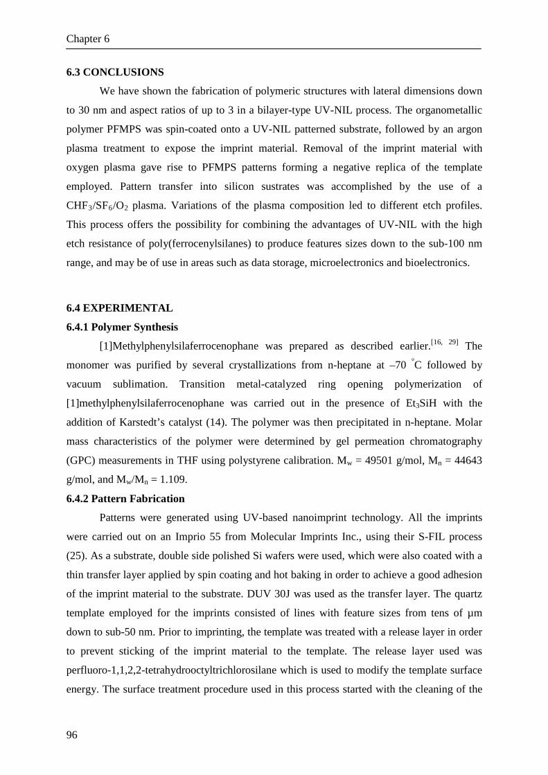
Chapter 6
96
6.3 CONCLUSIONS
We have shown the fabrication of polymeric structures with lateral dimensions down
to 30 nm and aspect ratios of up to 3 in a bilayer-type UV-NIL process. The organometallic
polymer PFMPS was spin-coated onto a UV-NIL patterned substrate, followed by an argon
plasma treatment to expose the imprint material. Removal of the imprint material with
oxygen plasma gave rise to PFMPS patterns forming a negative replica of the template
employed. Pattern transfer into silicon sustrates was accomplished by the use of a
CHF3/SF6/O2
plasma. Variations of the plasma composition led to different etch profiles.
This process offers the possibility for combining the advantages of UV-NIL with the high
etch resistance of poly(ferrocenylsilanes) to produce features sizes down to the sub-100 nm
range, and may be of use in areas such as data storage, microelectronics and bioelectronics.
6.4 EXPERIMENTAL
6.4.1 Polymer Synthesis
[1]Methylphenylsilaferrocenophane was prepared as described earlier.[16, 29] The
monomer was purified by several crystallizations from n-heptane at –70 °C followed by
vacuum sublimation. Transition metal-catalyzed ring opening polymerization of
[1]methylphenylsilaferrocenophane was carried out in the presence of Et3SiH with the
addition of Karstedt’s catalyst (14). The polymer was then precipitated in n-heptane. Molar
mass characteristics of the polymer were determined by gel permeation chromatography
(GPC) measurements in THF using polystyrene calibration. Mw = 49501 g/mol, Mn = 44643
g/mol, and Mw/Mn = 1.109.
6.4.2 Pattern Fabrication
Patterns were generated using UV-based nanoimprint technology. All the imprints
were carried out on an Imprio 55 from Molecular Imprints Inc., using their S-FIL process
(25). As a substrate, double side polished Si wafers were used, which were also coated with a
thin transfer layer applied by spin coating and hot baking in order to achieve a good adhesion
of the imprint material to the substrate. DUV 30J was used as the transfer layer. The quartz
template employed for the imprints consisted of lines with feature sizes from tens of µm
down to sub-50 nm. Prior to imprinting, the template was treated with a release layer in order
to prevent sticking of the imprint material to the template. The release layer used was
perfluoro-1,1,2,2-tetrahydrooctyltrichlorosilane which is used to modify the template surface
energy. The surface treatment procedure used in this process started with the cleaning of the

Nanoscale Patterning by UV-NIL
97
template with a piranha solution (conc. H2SO4 and 33% aq H2O2 in a 3:1 volume ratio,
Warning! piranha should be handled with caution; it can detonate unexpectedly) for 30 min
to remove any surface organic contaminants. After the piranha treatment, the substrates were
blown dry with N2 and reacted with the alkyltrichlorosilane (6). Imprinting was performed
using a low-viscosity acrylate-based organic SFIL resist. (Monomat, Molecular Imprints Inc.)
The imprint material was deposited by direct dispensing, where the volume was locally
adjusted to the pattern definition. After dispensing, the template was pressed into the still
liquid imprint material and held for 20 s under a pressure of 50 mbar to fill all the features.
Thereafter, the imprint material was cured by UV light irradiation through the transparent
template, followed by demolding.
6.4.3 Pattern Transfer
The synthesized PFMPS was spin coated on top of the imprinted resist. Argon plasma
sputtering was applied for 20-25 min (Ion Beam Etcher, 350 V, 6 mA) in order to expose the
organic imprint material. The imprinted resist features were subsequently etched with oxygen
plasma to expose the PFMPS lines. Oxygen reactive ion etching to remove the imprinted
resist was performed in an Elektrotech PF 340 apparatus (8 mTorr, 50 W, 20 sccm O2).
Etching into the substrate using the PFMPS lines as a template was enabled with different
mixtures of CHF3, O2 and SF6
SEM characterization was performed with a HR-LEO 1550 FEF SEM.
at a pressure of 10 mTorr. The resist was stripped off by
sonication for 1 h in 10% nitric acid solution followed by sonication in toluene.
6.5 ACKNOWLEDGEMENTS
We thank Mark Smithers for acquiring the SEM images.
6.6 REFERENCES
[1] S. Y. Chou, P. R. Krauss, P. J. Renstrom, Appl. Phys. Lett. 1995, 67, 3114.
[2] S. Y. Chou, P. R. Krauss, P. J. Renstrom, Science 1996, 272, 85.
[3] M. Bender, M. Otto, B. Hadam, B. Vratzov, B. Spangenberg, H. Kurz, Microelectron.
Eng. 2000, 53, 233.
[4] S. J. M.Colburn, M. Stewart, S. Dample, T. Bailey, B. Choi, M. Wedlake, T.
Michaelson, S. V. Sreenivasan, J. G. Ekerdt, C. G. Willson, Proc. SPIE 1999, 379.
[5] M. D. Stewart, S. C. Johnson, S. V. Sreenivasan, D. J. Resnick, C. G. Willson, J.
Microlithogr. Microfabr. Microsyst. 2005, 4.

Chapter 6
98
[6] T. Bailey, B. J. Choi, M. Colburn, M. Meissl, S. Shaya, J. G. Ekerdt, S. V.
Sreenivasan, C. G. Willson, J. Vac. Sci. Technol. B 2000, 18, 3572.
[7] J. H. Choi, S. W. Lee, D. G. Choi, K. D. Kim, J. H. Jeong, E. S. Lee, J. Vac. Sci.
Technol. B 2008, 26, 1390.
[8] H. Schmitt, L. Frey, H. Ryssel, M. Rommel, C. Lehrer, J. Vac. Sci. Technol. B 2007,
25, 785.
[9] N. Sakai, J. Taniguchi, K. Kawaguchi, M. Ohtaguchi, T. Hirasawa, J. Photopolym.
Sci. Technol. 2005, 18, 531.
[10] J. C. Eloi, L. Chabanne, G. R. Whittell, I. Manners, Mater. Today 2008, 11, 28.
[11] K. Kulbaba, I. Manners, Macromol. Rapid Commun. 2001, 22, 711.
[12] G. R. Whittell, I. Manners, Adv. Mater. 2007, 19, 3439.
[13] D. A. Foucher, B. Z. Tang, I. Manners, J. Am. Chem. Soc. 1992, 114, 6246.
[14] P. GomezElipe, P. M. Macdonald, I. Manners, Angew. Chem. Int. Ed. Engl. 1997, 36,
762.
[15] R. Rulkens, Y. Z. Ni, I. Manners, J. Am. Chem. Soc. 1994, 116, 12121.
[16] Y. Z. Ni, R. Rulkens, I. Manners, J. Am. Chem. Soc. 1996, 118, 4102.
[17] C. Kloninger, M. Rehahn, Macromolecules 2004, 37, 1720.
[18] R. G. H. Lammertink, M. A. Hempenius, V. Z. H. Chan, E. L. Thomas, G. J. Vancso,
Chem. Mater. 2001, 13, 429.
[19] I. Korczagin, R. G. H. Lammertink, M. A. Hempenius, S. Golze, G. J. Vancso, in
Ordered Polymeric Nanostructures at Surfaces, 200, 2006, 91.
[20] R. G. H. Lammertink, M. A. Hempenius, J. E. van den Enk, V. Z. H. Chan, E. L.
Thomas, G. J. Vancso, Adv. Mater. 2000, 12, 98.
[21] I. Korczagin, S. Golze, M. A. Hempenius, G. J. Vancso, Chem. Mater. 2003, 15,
3663.
[22] M. A. Hempenius, R. G. H. Lammertink, M. Peter, G. J. Vancso, Macromol. Symp.
2003, 196, 45.
[23] J. Y. Cheng, C. A. Ross, V. Z. H. Chan, E. L. Thomas, R. G. H. Lammertink, G. J.
Vancso, Adv. Mater. 2001, 13, 1174.
[24] C. Acikgoz, M. A. Hempenius, G. J. Vancso, J. Huskens, Nanotechnology 2009, 20,
135304.
[25] S. V. S. D. Resnick, C. G. Willson, Mater. Today 2005, 34.
[26] I. M. S. V. Sreenivasan, F. Xu, D. Wang, N. Stacey, Micro Magazine 2005.

Nanoscale Patterning by UV-NIL
99
[27] H. Jansen, M. Deboer, R. Legtenberg, M. Elwenspoek, J. Micromech. Microeng.
1995, 5, 115.
[28] R. Legtenberg, H. Jansen, M. Deboer, M. Elwenspoek, J. Electrochem. Soc. 1995,
142, 2020.
[29] K. Temple, J. A. Massey, Z. H. Chen, N. Vaidya, A. Berenbaum, M. D. Foster, I.
Manners, J. Inorg. Organomet. Polym. 1999, 9, 189.

Chapter 6
100

Chapter 7
Exploiting Nanoimprint Lithography for Polymer Brush
Engineering and Protein Immobilization
ABSTRACT. In this chapter the combination of step-and-flash imprint lithography and
surface initiated polymerization is described to obtain topologically and chemically patterned
surfaces. Following fabrication of patterns with lateral dimensions from several microns
down to the sub-100-nm range, the residual layer between the imprinted lines was etched
down to expose the silicon substrate. Self-assembled monolayers (SAMs) of initiators were
anchored to the exposed silicon, and brushes of polystyrene (PS), poly(glycidyl methacrylate)
(PGMA), and poly(ethylene glycol methacrylate) (PEGMA) were grown on the initiator-
covered areas. PEGMA brush structures were functionalized with succinic anhydride and
their swelling properties to different pH were investigated. The variety of the structures
enabled us to study the dependence of the size of the patterns on the height of the polymer
brush patterns. The functionalized patterned PEGMA layers were used for selective
immobilization of proteins. For this purpose, biotin and subsequently streptavidin were
immobilized on PEGMA brush layers. Protein patterns were successfully generated and AFM
analysis was used to calculate the amount of protein attached on a particular pattern.

Chapter 7
102
7.1 INTRODUCTION
Patterned nanostructures of polymer films have a wide range of applications in
biochips, biosensors and photonic crystal materials.[1-5] Stable, covalently bonded polymer
films represent a versatile tool to synthesize tunable platforms and allow one to tailor the
chemical, mechanical and energetic properties of surfaces. A covalent attachment of the
polymers to the surface is desirable especially in biological systems where the patterned
surface comes in contact with solvents and with other molecules which might lead to a
complete displacement of the polymer film and the loss of the pattern.[6] Different living
cationic,[7] anionic,[8] ring opening,[9] nitroxide mediated,[10] and atom transfer radical
polymerization[11] (ATRP) reactions have been successfully employed to give surface-grafted
polymers under controlled growth conditions providing excellent mechanical stability and
functionality and controllable brush length. The formation of dense polymer brushes is
possible through a grafting from approach in which covalently attached polymers are grown
by surface-initiated polymerization from the substrate (SIP).[12] In SIP, the polymer chains are
grown from surface-bound initiators which are self-assembled monolayers [13] of suitably
functionalized alkyl-chlorosilanes and alkanethiols. SIP could provide control over the shape,
feature dimensions and funtionality of brush architectures when it is combined with other
patterning techniques and would allow to fabricate macromolecular sensors, single-protein
platforms, antifouling surfaces and nano-fluidic devices with controlled dimensions.[14-16]
Several techniques such as photolithography, microcontact printing,[17, 18] chemical
lithography,[19] contact molding,[20] and electron beam lithography[14, 21, 22] have been
explored to pattern polymer brushes in combination with a grafting from approach. Of the
many patterning techniques studied, imprint lithography shows great promise since it is a
low-cost, high-throughput process and larger areas can be patterned simultaneously. Smaller
features could be fabricated by thermal imprinting[23, 24] or light-initiated polymerization[25]
(UV-NIL) and these techniques have circumvented many limitations of conventional
techniques.[26] Step-and-flash imprint lithography (SFIL), a UV-NIL variant, uses a
photocurable prepolymer solution as a resist to replicate the topography of a mold.[27] In
SFIL, a low viscosity, photocurable liquid or solution is not spin coated but dispensed in the
form of small droplets onto the substrate to fill the voids of the quartz mold. The solution
contains low molar mass monomer and a photoinitiator. Exposing this solution to UV light
cures the photopolymer to make a solidified replica while in contact with the mold.
Removing the mold leaves the inverse replica on the substrate. Because of the ability to
pattern at room temperature and at low pressure, the template can be stepped to pattern the
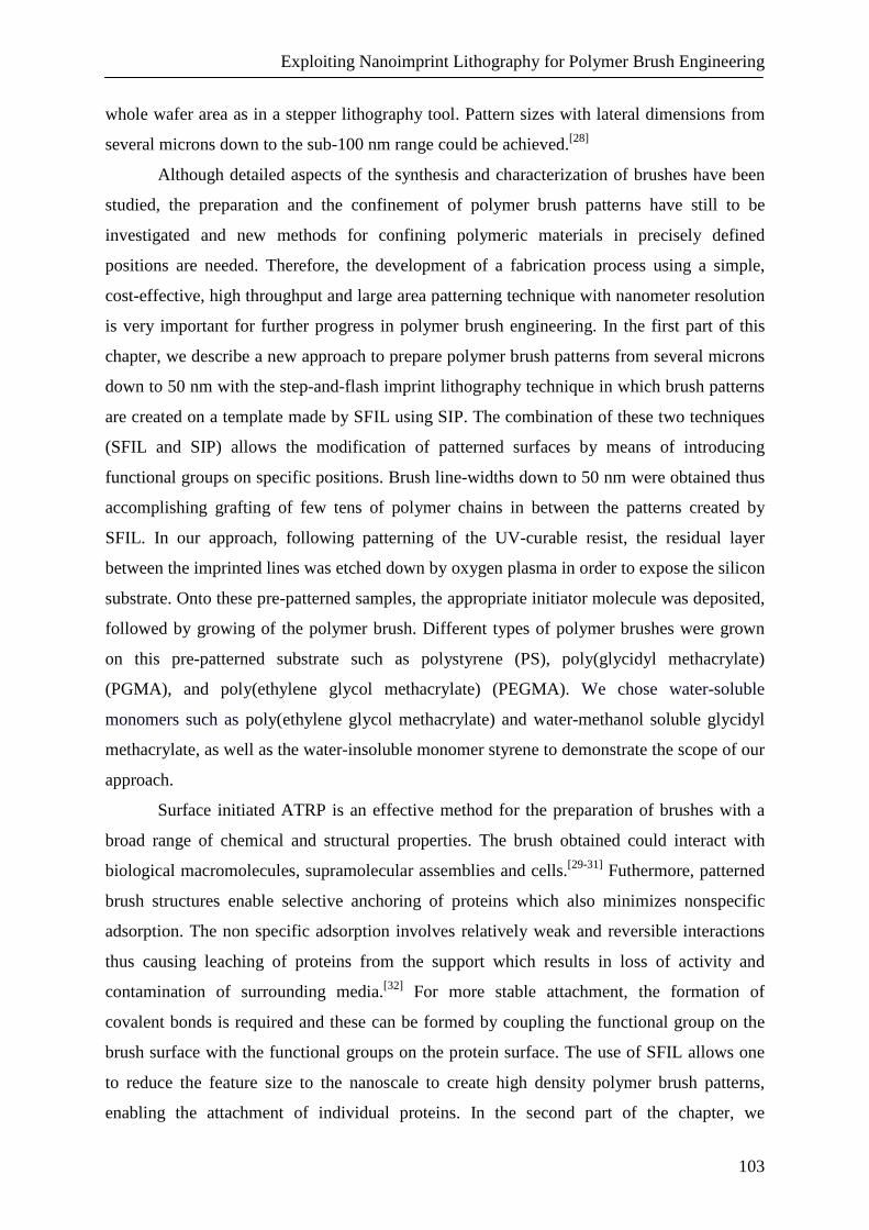
Exploiting Nanoimprint Lithography for Polymer Brush Engineering
103
whole wafer area as in a stepper lithography tool. Pattern sizes with lateral dimensions from
several microns down to the sub-100 nm range could be achieved.[28]
Although detailed aspects of the synthesis and characterization of brushes have been
studied, the preparation and the confinement of polymer brush patterns have still to be
investigated and new methods for confining polymeric materials in precisely defined
positions are needed. Therefore, the development of a fabrication process using a simple,
cost-effective, high throughput and large area patterning technique with nanometer resolution
is very important for further progress in polymer brush engineering. In the first part of this
chapter, we describe a new approach to prepare polymer brush patterns from several microns
down to 50 nm with the step-and-flash imprint lithography technique in which brush patterns
are created on a template made by SFIL using SIP. The combination of these two techniques
(SFIL and SIP) allows the modification of patterned surfaces by means of introducing
functional groups on specific positions. Brush line-widths down to 50 nm were obtained thus
accomplishing grafting of few tens of polymer chains in between the patterns created by
SFIL. In our approach, following patterning of the UV-curable resist, the residual layer
between the imprinted lines was etched down by oxygen plasma in order to expose the silicon
substrate. Onto these pre-patterned samples, the appropriate initiator molecule was deposited,
followed by growing of the polymer brush. Different types of polymer brushes were grown
on this pre-patterned substrate such as polystyrene (PS), poly(glycidyl methacrylate)
(PGMA), and poly(ethylene glycol methacrylate) (PEGMA). We chose water-soluble
monomers such as poly(ethylene glycol methacrylate) and water-methanol soluble glycidyl
methacrylate, as well as the water-insoluble monomer styrene to demonstrate the scope of our
approach.
Surface initiated ATRP is an effective method for the preparation of brushes with a
broad range of chemical and structural properties. The brush obtained could interact with
biological macromolecules, supramolecular assemblies and cells.[29-31] Futhermore, patterned
brush structures enable selective anchoring of proteins which also minimizes nonspecific
adsorption. The non specific adsorption involves relatively weak and reversible interactions
thus causing leaching of proteins from the support which results in loss of activity and
contamination of surrounding media.[32] For more stable attachment, the formation of
covalent bonds is required and these can be formed by coupling the functional group on the
brush surface with the functional groups on the protein surface. The use of SFIL allows one
to reduce the feature size to the nanoscale to create high density polymer brush patterns,
enabling the attachment of individual proteins. In the second part of the chapter, we
Chapter 7
104
demonstrate the use of patterned PEGMA brushes as platforms for immobilization of
proteins. To immobilize proteins, the brush patterned substrate was initially passivated with
poly(ethylene oxide)-silane monolayers to prevent nonspecific adsorption in the grooves of
the brush patterns. Then PEGMA was modified sequentially with succinic anhydride (SA), 1-
ethyl-3-(3-dimethylaminopropyl)-carbodiimide (EDC) and N-hydroxysuccinimide (NHS),
amino-biotin and finally streptavidin. The structure and morphology of the graft-
functionalized silicon surfaces were characterized by Fourier transform infrared (FTIR)
spectroscopy, and atomic force microscopy (AFM).
7.2 RESULTS & DISCUSSION
7.2.1 Preparation and Characterization of Brushes
Figure 7.1 shows the fabrication scheme of patterned polymer brushes via the
combination of SFIL[27] and SIP. In the SFIL process, the acrylate based imprint material was
dispensed onto the transfer layer-coated substrates, and the template was brought into contact
with the still liquid imprint material. The transfer layer provided a good adhesion of the
imprint material to the substrate. After exposure and curing of the imprint material, the
template was demolded from the substrate, leaving its negative 3D image. To expose the
silicon substrate in the grooves of the imprinted structures, the residual layer was removed by
exposure to an oxygen plasma. The wafers were then reacted with an ATRP initiator and
polymer brushes were grown from the ATRP initiator-covered regions. After polymerization,
the resist lines were removed via sonication. In this process, the imprinted polymeric
structures were used as template to grow brushes and the polymer template was removed
following the brush synthesis. The removal of the polymer template could be also performed
before brush synthesis but since the resist monomer was crosslinked upon UV-curing, the
template formed can withstand subsequent polymerization conditions and stay intact during
brush synthesis.

Exploiting Nanoimprint Lithography for Polymer Brush Engineering
105
Figure 7.1 Fabrication process for creating polymer brush patterns.
The template used in the S-FILTM process has patterns consisting of lines of 500 nm
to 100 nm wide with pitches of 1:1, 1:2, 1:3, 1:4, 1:5 and with a height of 100 nm. The same
template contains pillars and grooves with widths of 70 nm to 200 nm. Figure 7.2a shows the
line patterns of 100 nm width onto a substrate with pitches of 1:1, 1:2 and 1:3 created on a
substrate with this template. Figure 7.2b shows a cross-section image of the imprinted lines.
As seen here, the combined thickness of the transfer layer and residual UV-curable resist
layer following imprinting was about 40 nm. This rather thin residual layer thickness was
achieved by optimizing the dispensing conditions. Subsequently, the samples were treated
with oxygen plasma during which the exposed organic imprint layer and the transfer layer
material underneath were removed. A short exposure time to oxygen plasma was sufficient to
remove the imprint material down to the substrate as shown in Figure 7.2c. The height of the
features of the lines after imprinting was around 100 nm. Following etching the exposed
silicon oxide substrate was functionalized with the ATRP initiator which contains a
bromoisobutyryl group.

Chapter 7
106
Figure 7.2 SEM images of UV-imprinted structures of (a) lines of 100 nm wide with pitches
of 1:1, 1:2 and 1:3 and with a height of 100 nm. (b) SEM images of lines of 200 nm wide
showing the total thickness of the residual UV-curable resist layer and the transfer layer. (c)
SEM image of lines of 150 nm wide after removal of the residual layer by O2 RIE.
Growth of dense brushes of PEGMA (Figure 7.3a) on silicon substrates by atom
transfer radical polymerization was reported earlier by Xu et al.[33] In our case, using the
prepatterned substrate, PEGMA brushes were obtained with the CuCl/CuBr2/bipy catalyst
system in aqueous solution at room temperature on prepatterned substrates (Figure 7.3b). The
morphology of polymer brushes formed on the surfaces was investigated with tapping mode
AFM imaging. Figure 7.3c captures an image of the PEGMA brushes after removal of the
resist lines via sonication in acetone. Removal of the imprint material gave rise to PEGMA
brush patterns forming a negative replica of the template employed (Figure 7.3c). The height
of the brushes after polymerization was around 70 nm after 1 hour of polymerization as
determined with AFM analysis (Figure 7.3d).
In order to prove the effective removal of the resist lines between the brush patterns,
AFM and SEM analysis were performed. An AFM phase image (Figure 7.4e) shows the clear
contrast between the brush (bright areas) and bare silicon surface (dark areas) and confirms
the absence of any residual layer. In addition, the SEM image (Figure 7.4f) recorded for the
same sample confirms that well‐contrasted silicon regions can be recognized in between the
brush patterns.

Exploiting Nanoimprint Lithography for Polymer Brush Engineering
107
Figure 7.3 (a) Schematic of PEGMA brushes. (b) AFM image of the resist lines of 250 nm
with a pitch of 1.2 obtained after etching. (c) AFM image of PEGMA brushes obtained after
removal of the resist lines. (d) AFM height profile of the AFM image (c). (e) AFM image of
corresponding AFM image (c). (e) SEM image of brush lines after resist removal.
The width of the polymer brushes obtained by using this approach strongly depends
on the lateral feature width of the patterns.[34, 35] Figure 7.4a-e shows AFM images of a series
of patterns after polymerization with resist patterns and Figure 7.4f-l shows brush patterns
after polymerization and subsequent resist removal. The resist patterns used encompasses a
series of 100 nm lines with 1:1, 1:2, 1:3, 1:4, 1:5 lateral distances, respectively. A typical
imprinted series resulted in brush patterns characterized by average widths ranging from 500
for the 1:5 distance to 80 nm for the 1:1 distance (Figure f and l). Height values varied
ranging from 80 to 30 nm (for the widest and narrowest patterns, respectively).

Chapter 7
108
Figure 7.4 AFM images of a series of patterns after polymerization with resist patterns (a-e)
and brush patterns after polymerization and subsequent resist removal (f-l).
As the lateral distance between the resist lines gets smaller, size effects becomes more
evident and the brush height significantly decreases.[35] The AFM height profiles of the
samples are displayed in Figure 7.5A before (grey cross-sections) and following (black cross-
sections) removal of the resist lines for AFM imaging (see Figure 7.4a-l). In the graph in
Figure 7.5B, the width/height of different brush patterns are plotted as a function of the
average line-to-line resist distance. As it is clearly shown in the plot, not only the width of the
brush features decreases when the resist lines are closer to each other, but also the height of
the features follows a similar trend. When the distance between the resist lines increases, the
height of the polymer brushes approaches the value of the thickness of the homogenous
polymer film on unpatterned surface as one would anticipate. This behaviour is thought to be
related to the density of initiator sites or to a monomer diffusion limitation which become
more important when resist lines are more closely spaced. Polymer chains at the domain
boundaries extend into the surrounding polymer-free areas resulting in a decrease in the
height of the brush which could also explain the observed height decrease.[35]

Exploiting Nanoimprint Lithography for Polymer Brush Engineering
109
Figure 7.5 (A) Graph showing the height profile before before (grey cross-sections) and
following (black cross-sections) removal of the resist lines. (B) Height vs width of brush
patterns plotted as a function of the average line-to-line resist distance.
The S-FIL technique in principle allows one to achieve patterning on the nanometer
scale which is one of the main advantages of this technique. Employing this method, we
demonstrate the fabrication of polymer hedge-brushes of PEGMA having a width of 60 nm
and a height of 10 nm (Figure 7.6). According to the lateral width of these features the
constituent brush structures are formed by a few tens of grafted macromolecules.
Figure 7.6 AFM image of polymer hedge-brushes of PEGMA obtained with high resolution.

Chapter 7
110
To show the versatility of the approach, PS and PGMA brushes were grown on pre-
patterned samples as well. PS brushes were synthesized from initiator-modified silicon
substrates by ATRP at 60 ̊C (as shown in Figure 7.1).[8, 13] The height of the brushes obtained
after 12 h of polymerization was 40 nm. The AFM image in Figure 7.7a shows the PS brush
patterns with a lateral distance of 100 nm. The pillars (Figure 7.7b) have a width of
approximately 40 nm after polymerization and variations in size have been observed. This
could be due to swelling behavior of the resist during polymerization since was performed at
high T and in bulk. The FTIR spectrum in Figure 7.7c shows the absorption bands
corresponding to the symmetric and asymmetric stretching vibration of C–H along the main
chain of PS appear between 2800 - 3000 cm-1, whereas those at 3000 - 3200 cm-1are assigned
to the stretching vibration of the aryl C–H.
Figure 7.7 AFM images (a, b) and FTIR spectrum (c) of fabricated PS brushes
PGMA brushes may serve as a platform for many applications due to the presence of
the epoxide functionalities and thus a chemical functionality which can be further
exploited.[18, 36] PGMA brushes were grown by aqueous ATRP as reported earlier.[36] The
PGMA structures were analyzed by AFM (Figure 7.8a). The height of the brushes was
around 50 nm and they were highly uniform over large areas as seen in Figure 7.8b. FTIR
shows the epoxide group peak at around 910 cm-1 which is a characteristic fingerprint of this
moiety (Figure 7.8c).

Exploiting Nanoimprint Lithography for Polymer Brush Engineering
111
Figure 7.8 AFM images (a, b) and FTIR spectrum (c) of PGMA brushes.
7.2.2 PEGMA Brushes as Platforms for Immobilization of Proteins
To be used in biological applications, patterns must fulfill specific requirements, one
of which is to create bio-interactive patterns in a non-interactive background. Poly(ethylene
glycol)s (PEG)s are commonly used for the preparation of antifouling surfaces. Herein, we
covalently couple proteins onto the protein resistant (biologically inert) PEG- based brushes
by reacting the hydroxyl group of the PEG brushes via succinic anhydride (SA) and later on
by NHS-assisted coupling of the specific biomolecules, thus ensuring a high ratio of specific
to non-specific binding.[37] In order to achieve a selective immobilization onto the
brush‐hedge structures avoiding nonspecific adsorption to the surrounding substrate, the
exposed silicon oxide surface was previously passivated via anchoring of PEO‐silane species.
Biotin/streptavidin[38, 39] bioconjugates have been used as a model system to study the
selective protein immobilization on patterned brushes and brush-hedge structures.
Streptavidin with the highly specific interaction to the complementary biotin offers many
advantages since the selective and specific interaction between them has been proven while
simultaneously all other non-specific binding is being minimized. After binding of
streptavidin is optimized with two remaining binding sites facing the aqueous phase, they can
be used to bind and organize other functional units like antibodies, their fragments, colloids,
oligonucleotides.[39] For immobilization, PEGMA surfaces were first activated and then
reacted with biotin-PEG(10)-NH2 and subsequently with streptavidin in PBS solution (Figure
7.9).

Chapter 7
112
Figure 7.9 Schematics of brush functionalization with proteins and pH-responsive behavior.
PEGMA brush patterns were reacted with succinic anhydride in order to introduce
carboxylic acid moieties along the polymer backbones (Figure 7.9). PEGMA samples having
a thickness of 70 nm (Figure 7.10a) were incubated for 10 h in a dry pyridine solution of
succinic anhydride. Following the reaction, the thickness was measured with AFM and
determined to be 80 nm (Figure 7.10b). The increase in the thickness is due to the expected
volume increase of the monomer units constituting the brushes (Figure 7.10c). Due to the
presence of carboxylic acid moieties in the brush architecture, succinic anhydride
functionalized PEGMA brushes display pH-dependent swelling properties. At pH 3.0 the
polymer chains are protonated and charge neutral, and they display an average height value
of 36 nm and width of 131 nm indistinguishable from the average dry height (Figure 7.11a).
When the brush hedges are immersed in a pH 7.0 buffer solution, negative charges
accumulate inside the brush structure, thus producing a profused swelling increment (Figure
7.11b). In this case, the average height value increases to 59 nm while the width reaches 140
nm. The graph plotted in Figure 7.11c (height vs pattern) clearly displays the pH-responsive
behavior of the brush patterns.
Exploiting Nanoimprint Lithography for Polymer Brush Engineering
113
Figure 7.10 (a) AFM height image of PEGMA brush before treatment with SA. (b) AFM
image of PEGMA brush after treatment with SA. (c) Cross sectional plot with (a) and (b)
showing the height increase after SA treatment.
Figure 7.11 pH responsive behavior of PEGMA brushes after treatment with SA (a) at pH
3.0, (b) at pH 7.0. (c) Average brush height plotted as a function of pattern size at pH 3 and at
pH 7.0.
FTIR spectra depicted in Figure 7.12 reveal the presence of signals corresponding to
the desired functionalities of the polymer brushes discussed earlier. FTIR spectra were taken
on continuous brush films which underwent the same treatments with respect to the patterned
samples. The FTIR spectrum of the PEGMA surface displays the presence of two major

Chapter 7
114
absorption bands in the 1700 and 1140 cm-1 region, arising from the stretching of the ester
carbonyl group and the C-O-C group, respectively. As it can be seen in Figure 7.13b, after
succinic anhydride functionalization the OH band completely disappeared and the intensity of
C=O signal (1700 cm-1) increased as compared to the signal in Figure 7.13a. The increase in
height of this peak reflected an increase in C=O content along the PEGMA chain. Each step
of the protein immobilization process was monitored by FTIR. Reaction with NHS-EDC
resulted in the characteristic peaks shown in Figure 7.13c. The shoulder peaks at 1710 cm-1
and 1720 cm-1 are assigned to the carbon stretching of NHS. The peak at 1070 cm-1 in Figure
7.13c is assigned to the C-N stretching. Reaction with biotin-PEG(10)-NH2 results in a peak
at 1680 cm-1 due to the amide stretching vibration of biotin (Figure 7.13d). The FTIR
spectrum of the streptavidin functionalized film shows the absorption corresponding to amide
I and II bands at 1700-1600 cm-1 and 1600-1500 cm-1, respectively (Figure 7.13e).
Figure 7.12 FTIR spectra obtained for a) PEGMA brushes, (b) PEGMA reacted with SA, (c)
after reaction with NHS-EDC, (d) following amide bond formation with biotin, (e) final
reaction with streptavidin.
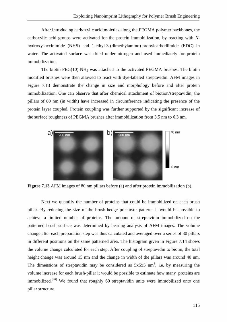
Exploiting Nanoimprint Lithography for Polymer Brush Engineering
115
After introducing carboxylic acid moieties along the PEGMA polymer backbones, the
carboxylic acid groups were activated for the protein immobilization, by reacting with N-
hydroxysuccinimide (NHS) and 1-ethyl-3-(dimethylamino)-propylcarbodiimide (EDC) in
water. The activated surface was dried under nitrogen and used immediately for protein
immobilization.
The biotin-PEG(10)-NH2 was attached to the activated PEGMA brushes. The biotin
modified brushes were then allowed to react with dye-labeled streptavidin. AFM images in
Figure 7.13 demonstrate the change in size and morphology before and after protein
immobilization. One can observe that after chemical attachment of biotion/streptavidin, the
pillars of 80 nm (in width) have increased in circumference indicating the presence of the
protein layer coupled. Protein coupling was further supported by the significant increase of
the surface roughness of PEGMA brushes after immobilization from 3.5 nm to 6.3 nm.
Figure 7.13 AFM images of 80 nm pillars before (a) and after protein immobilization (b).
Next we quantify the number of proteins that could be immobilized on each brush
pillar. By reducing the size of the brush-hedge precursor patterns it would be possible to
achieve a limited number of proteins. The amount of streptavidin immobilized on the
patterned brush surface was determined by bearing analysis of AFM images. The volume
change after each preparation step was thus calculated and averaged over a series of 30 pillars
in different positions on the same patterned area. The histogram given in Figure 7.14 shows
the volume change calculated for each step. After coupling of streptavidin to biotin, the total
height change was around 15 nm and the change in width of the pillars was around 40 nm.
The dimensions of streptavidin may be considered as 5x5x5 nm3, i.e. by measuring the
volume increase for each brush-pillar it would be possible to estimate how many proteins are
immobilized.[40] We found that roughly 60 streptavidin units were immobilized onto one
pillar structure.

Chapter 7
116
PP-S
A
P-SA_
NHS
P-SA_
biotin
P-SA_
strep
tavidi
n0
100000
200000
300000
400000
500000
Tota
l vol
ume
of o
ne p
illar
(nm
3 )
Figure 7.14 Histogram showing the volume of PEGMA brushes, PEGMA brushes were
reacted with SA, activated with EDC-NHS, coupled with biotin and finally immobilized with
streptavidin(y axis is in nm3).
Further evidence for the attachament of biotin and streptavidin is provided by
fluorescence microscopy (Figure 7.15). The green lines indicate the presence of streptavidin,
which coincides with the brush patterns. Binding occurs only to the brush patterns, not to
regions in between the brush patterns (dark regions). The results indicate that streptavidin
was only bound to the regions where biotin was present on the brush patterns. In addition, the
regions between the patterns were successfully passivated and no nonspecific absorption of
protein was observed within these regions.

Exploiting Nanoimprint Lithography for Polymer Brush Engineering
117
Figure 7.15 Fluorescence microscopy images of patterned PEGMA brushes coupled with
biotin/streptavidin.
7.3 CONCLUSIONS
We presented a simple but versatile method to fabricate polymer brush patterns by
combining SFIL and SIP. Patterns created by SFIL were further used for anchoring SAM of
initiator for performing SIP. The method allowed controlled preparation of brush patterns of
PEGMA, PS and PGMA with lateral dimensions ranging from several microns down to 40
nm. Such variations in domain size enabled the study of the dependence of the width of the
pattern on the height/width of the brush structures. It was shown that nanosized domains
exhibit a significantly reduced height. The functionalization of PEGMA brush patterns was
demonstrated. Due to the presence of carboxylic acid moieties in the PEGMA brush
architecture, these brushes exhibit controlled swelling at different pH values, which was
monitored by AFM. The structurally robust and functional patterned PEGMA polymeric
nanostructures obtained enabled protein immobilization. Streptavidin/biotin were selectively
coupled on the activated PEGMA brush patterns. This approach is very promising for
fabricating protein patterns which could be integrated into microfabricated devices and
sensors.
7.4 EXPERIMENTAL
7.4.1 Pattern Fabrication
Patterns were generated using UV-based nanoimprint technology. All imprints were
carried out on an Imprio 55 from Molecular Imprints Inc., using the S-FIL process.[28] As a
substrate, double side polished Si wafers were used, which were also coated with a thin
transfer layer applied by spin coating and hot baking in order to achieve a good adhesion of
the imprint material to the substrate. DUV 30J was used as the transfer layer. The quartz

Chapter 7
118
template employed for the imprints consisted of lines, pillars, and groves with feature sizes
from tens of µm down to sub-50 nm. Prior to imprinting, the template was treated with a
release layer of perfluoro-1,1,2,2-tetrahydrooctyltrichlorosilane in order to prevent sticking of
the imprint material to the template. The surface treatment procedure used in this process
started with the cleaning of the template with a piranha solution (conc. H2SO4 and 33% aq
H2O2 in a 3:1 volume ratio, Warning! Piranha should be handled with caution; it can detonate unexpectedly) for 30 min to remove any organic contaminants from the surface.
Following the piranha treatment, the substrates were blown dry with N2 and reacted with the
alkyltrichlorosilane. Imprinting was performed using a low-viscosity acrylate-based organic
SFIL resist. (Monomat, Molecular Imprints Inc.) The imprint material was deposited by
direct dispensing, where the volume was locally adjusted to the pattern definition. After
dispensing, the template was pressed into the still liquid imprint material and held for 20 s
under a pressure of 50 mbar to fill all the features. Thereafter, the imprint material was cured
by UV light irradiation through the transparent template, followed by demolding. Oxygen
reactive ion etching to remove the residual layer was performed in an Elektrotech PF 340
apparatus (10 mTorr, 10 W, 10 sccm O2
7.4.2 Preparation, Functionalization and Characterization of Brushes
) for 70 sec. As an initiator 3-
(chlorodimethylsilyl)proply 2-bromo-2-methylpropionate was used and the synthesis of the
initiator was shown before. The initiator was anchored to a surface by gas-phase evaporation
in a desiccator under vacuum.
7.4.2.1 Surface-initiated ATRP of PEGMA
CuBr2 was purchased from Aldrich and used as received. CuCl was purified by
washing glacial acetic acid and, after filtration by rinsing with ethanol and acetone.
Poly(ethylene glycol methacrylate) with an average molecular weight of 360 Da was
purchased from Sigma and subsequently purified from inhibitors employing basic alumina
column. In a typical ATRP 0.162 g of bipyridine were added to a mixture of 7.5 g of PEGMA
360 and 7.5 g of water. This solution was degassed by three freeze-thaw-pump cycles and
later on transferred, via a degassed syringe, to a second flask containing CuCl (41.18 mg),
CuBr2
(9.2 mg). The resulting mixture was stirred at ambient temperature for 30 minutes,
until complete formation of dark-brown complex. Subsequently, the reaction solution was
transferred, via a degassed syringe, into an argon purged flask containing the ATRP initiator
functionalized samples. The polymerization was carried out for 1 h at room temperature
under nitrogen.

Exploiting Nanoimprint Lithography for Polymer Brush Engineering
119
7.4.2.2 Surface-initiated ATRP of PGMA
PGMA was purchased from Aldrich and subsequently purified from inhibitors by
employing a basic aluminum oxide column. A solution of glycidyl methacrylate (5 ml, 5.21
g) in methanol and water (1 ml) was degassed by bubbling through argon for 15 min. To this
solution added CuCl (36.4 mg), CuBr2
7.4.2.3 Surface-initiated ATRP of PS
(3.9 mg), and 2,2’-dipyridyl (141 mg). To dissolve all
solids, the mixture was stirred for 5 min while degassing continued, giving a dark brown
solution. After stirring, the reaction solution was transferred, via a degassed syringe, into an
argon purged flask containing the ATRP initiator functionalized samples. The polymerization
had been allowed to proceed for 1 hour and then the sample was removed and washed with
methanol and water, followed by dichloromethane and dried under a nitrogen stream.
Styrene was purchased from Aldrich and subsequently purified from inhibitors
employing a basic aluminum oxide column. Polymerization of styrene from the ATRP
initiator coated silicon substrates was carried out in bulk conditions (Styrene concentration
8.6 M). The catalyst comprised of Cu(I)Br and ligand, PMDETA, with a molar ratio of 1:1
and a catalyst concentration of 8.6 × 10⁻²
7.4.2.4 Functionalization of Brushes and pH responsive
M. The monomer was degassed by three freeze-
pump-thaw cycles and then transferred to the catalyst with maximum precautions to avoid
oxygen. After stirring, the reaction solution was transferred, via a degassed syringe , into an
argon purged flask containing the ATRP initiator functionalized samples . The polymerization
was carried out at 60 ̊C overnight under an Ar stream.
Before functionalization the of PEGMA brushes, the samples were immersed in dry
toluene solution of 2-[methoxy(polyethyleneoxy)propyl]trimethoxysilane overnight under an
Ar stream for passivation.
PEGMA-based brush films were derivatized with succinic anhydride by overnight
reaction in 30 mg/ml dry pyridine solution. The pH was adjusted by adding 0.1 M HCl or 0.1
M NaOH to the aqueous solutions.
The derivatized PEGMA brush films were activated by immersion in an aqueous
solution of EDC (1 M) and NHS (0.2 M) for 30 min. The samples were then rinsed with
Milli-Q water, dried in a stream of nitrogen, and used immediately thereafter.
7.4.2.5 Characterization
Surface morphology images of the fabricated brush films were recorded by tapping
mode atomic force microscopy. Contact mode AFM imaging was performed using a liquid

Chapter 7
120
cell setup in order to determine the swelling properties of the brush films at different pH
values.
FTIR-spectra (spectral resolution of 8 cm-1
SEM images were taken with a HR-LEO 1550 FEF SEM. No sample surface coating
was applied.
, 2048 scans) were obtained using a BIO-
RAD FTS575C FTIR spectrometer equipped with a nitrogen-cooled cryogenic cadmium
mercury telluride detector. Background spectra were obtained by scanning a clean silicon
substrate.
7.4.3 Protein Immobilization
Following activation of surfaces with EDC/NHS, the samples were incubated in PBS
solution of biotin-PEG (10) NH2
7.5 ACKNOWLEDGEMENT
overnight (1 µM). Biotin functionalized surfaces were
immersed PBS solution of streptavidin (1 µM) overnight.
We thank Mark Smithers for acquiring the SEM images.
7.6 REFERENCES
[1] M. Geissler, Y. N. Xia, Adv. Mater. 2004, 16, 1249.
[2] H. Tu, C. E. Heitzman, P. V. Braun, Langmuir 2004, 20, 8313.
[3] C. D. H. Alarcon, T. Farhan, V. L. Osborne, W. T. S. Huck, C. Alexander, J. Mater.
Chem. 2005, 15, 2089.
[4] N. Mahajan, R. B. Lu, S. T. Wu, J. Y. Fang, Langmuir 2005, 21, 3132.
[5] P. T. Hammond, Adv. Mater. 2004, 16, 1271.
[6] O. Prucker, J. Habicht, I. J. Park, J. Ruhe, Mater. Sci. Engin. C 1999, 8-9, 291.
[7] M. D. K. Ingall, C. H. Honeyman, J. V. Mercure, P. A. Bianconi, R. R. Kunz, J. Am.
Chem. Soc. 1999, 121, 3607.
[8] R. Jordan, A. Ulman, J. F. Kang, M. H. Rafailovich, J. Sokolov, J. Am. Chem. Soc.
1999, 121, 1016.
[9] M. Weck, J. J. Jackiw, R. R. Rossi, P. S. Weiss, R. H. Grubbs, J. Am. Chem. Soc.
1999, 121, 4088.
[10] M. Husemann, M. Morrison, D. Benoit, K. J. Frommer, C. M. Mate, W. D. Hinsberg,
J. L. Hedrick, C. J. Hawker, J. Am. Chem. Soc. 2000, 122, 1844.
[11] X. Huang, M. J. Wirth, Macromolecules 1999, 32, 1694.
[12] O. Prucker, J. Ruhe, Langmuir 1998, 14, 6893.

Exploiting Nanoimprint Lithography for Polymer Brush Engineering
121
[13] A. Samadi, S. M. Husson, Y. Liu, I. Luzinov, S. M. Kilbey, Macromol. Rapid
Commun. 2005, 26, 1829.
[14] S. J. Ahn, M. Kaholek, W. K. Lee, B. LaMattina, T. H. LaBean, S. Zauscher, Adv.
Mater. 2004, 16, 2141.
[15] R. C. Bailey, J. T. Hupp, Anal. Chem. 2003, 75, 2392.
[16] N. Nath, A. Chilkoti, Adv. Mater. 2002, 14, 1243.
[17] M. Husemann, D. Mecerreyes, C. J. Hawker, J. L. Hedrick, R. Shah, N. L. Abbott,
Angew. Chem. Int. Ed. 1999, 38, 647.
[18] D. M. Jones, W. T. S. Huck, Adv. Mater. 2001, 13, 1256.
[19] U. Schmelmer, R. Jordan, W. Geyer, W. Eck, A. Golzhauser, M. Grunze, A. Ulman,
Angew. Chem. Int. Ed. 2003, 42, 559.
[20] T. A. von Werne, D. S. Germack, E. C. Hagberg, V. V. Sheares, C. J. Hawker, K. R.
Carter, J. Am. Chem. Soc. 2003, 125, 3831.
[21] U. Schmelmer, A. Paul, A. Kuller, M. Steenackers, A. Ulman, M. Grunze, A.
Golzhauser, R. Jordan, Small 2007, 3, 459.
[22] Y. Tsujii, M. Ejaz, S. Yamamoto, T. Fukuda, K. Shigeto, K. Mibu, T. Shinjo, Polymer
2002, 43, 3837.
[23] S. Y. Chou, P. R. Krauss, P. J. Renstrom, J. Vac. Sci. Technol. B 1996, 14, 4129.
[24] S. Y. Chou, P. R. Krauss, P. J. Renstrom, Science 1996, 272, 85.
[25] M. Bender, M. Otto, B. Hadam, B. Vratzov, B. Spangenberg, H. Kurz, Microelectron.
Eng. 2000, 53, 233.
[26] B. D. Gates, Q. B. Xu, M. Stewart, D. Ryan, C. G. Willson, G. M. Whitesides, Chem.
Rev. 2005, 105, 1171.
[27] D. Resnick, S. V. Sreenivasan, C. G. Willson, Mater. Today 2005, 34.
[28] S. V. Sreenivasan, I. McMackin, F. Xu, D. Wang, N. Stacey, Micro Magazine 2005.
[29] J. Nicolas, G. Mantovani, D. M. Haddleton, Macromol. Rapid Commun. 2007, 28,
1083.
[30] S. Zauscher, A. Chilkoti, Biointerphases 2009, 4, FA1.
[31] R. Dong, S. Krishnan, B. A. Baird, M. Lindau, C. K. Ober, Biomacromolecules 2007,
8, 3082.
[32] L. S. Wong, F. Khan, J. Micklefield, Chem. Rev. 2009, 109, 4025.
[33] D. Xu, W. H. Yu, E. T. Kang, K. G. Neoh, J. Colloid Interface Sci. 2004, 279, 78.
[34] W. K. Lee, M. Patra, P. Linse, S. Zauscher, Small 2007, 3, 63.

Chapter 7
122
[35] M. Mathieu, A. Friebe, S. Franzka, M. Ulbricht, N. Hartmann, Langmuir 2009, 25,
12393.
[36] S. Edmondson, W. T. S. Huck, J. Mater. Chem. 2004, 14, 730.
[37] F. J. Xu, H. Z. Li, J. Li, Y. H. E. Teo, C. X. Zhu, E. T. Kang, K. G. Neoh, Biosens.
Bioelectron. 2008, 24, 773.
[38] Z. L. Ding, R. B. Fong, C. J. Long, P. S. Stayton, A. S. Hoffman, Nature 2001, 411,
59.
[39] P. Jonkheijm, D. Weinrich, H. Schroder, C. M. Niemeyer, H. Waldmann, Angew.
Chem. Int. Ed. 2008, 47, 9618.
[40] A. Arakaki, S. Hideshima, T. Nakagawa, D. Niwa, T. Tanaka, T. Matsunaga, T.
Osaka, Biotechnol. Bioeng. 2004, 88, 543.

Chapter 8
Size Distribution of Microdomains in Spherical Morphology
Polystyrene-polyferrocenyldimethylsilane Block copolymer Thin
Films
ABSTRACT. Thin films of organic-organometallic block copolymers have been used in
bottom-up lithography because of the high etch selectivity between the two blocks and the
etch resistance of the organometallic block. The study in this chapter investigates the effects
of volume fraction, molecular weight, and polydispersity index (PDI) on the distribution of
the size and spacing of the spherical microdomains of thin films of polystyrene-block-
polyferrocenyldimethylsilane (PS-b-PFS) block copolymers which are comprised of a
monolayer of PFS microdomains. Size and spacing distributions depend on volume fraction,
but have little dependence on PDI and molecular weight. The minor effects of PDI are
attributed to the statistical variation in the number of chain ends per microdomain, which is
only 7% of the total number of chain ends per PFS microdomain.

Chapter 8
124
8.1 INTRODUCTION
As the size of electronic and magnetic devices decreases, strategies to accomplish
planar processing on the nanoscale have become increasingly important. Patterning is
conventionally achieved using top-down lithographic processes such as optical or electron-
beam lithography, but the resolution of optical lithography is limited to ~50 nm for 193 nm
wavelength, while electron-beam lithography is too slow for manufacturing. Instead, bottom-
up methods based on self-assembly have been explored for their potential to create high-
throughput nanoscale patterns suitable for nanolithography. Diblock copolymers form a
variety of well-ordered morphologies depending on the volume fractions of the two
constituents with nanoscale periodicity,[1] and have been widely studied for lithographic
patterning.[2-12] The size and the periods of the microdomains are governed by the chain
dimensions and are typically on the order of 10 nm. Structures smaller than 10 nm are also
obtainable if one chooses appropriate blocks with a high Flory-Huggins interaction
parameter[1] and decreases the block lengths. The periodic patterns, including spheres,
cylinders or lamella generated by block copolymers, are particularly well suited for
applications requiring periodic arrays of nanostructures, for example for the fabrication of
high-density patterned magnetic recording media where a 25 nm periodicity would
correspond to up to 1 Tb/in2 of data density.[4, 13] Futhermore, each block of the copolymer
can be used for a specific application, and selective removal of one block relative to the other
one is possible by use of chemical and physical dissimilarities between the two blocks.
Much work on block copolymer lithography has been carried out using polystyrene-b-
polymethylmethacrylate (PS-b-PMMA), which has excellent etch selectivity between the two
blocks, allowing the PMMA to be removed upon plasma treatment.[14, 15] However, the
remaining PS microdomains have a low etch resistance, which limits subsequent pattern
transfer steps. In order to be used in the lithography process, the block copolymer film also
must be compatible with the etch process. To obtain a pattern with higher etch resistance,
block copolymers containing both an organic block and an organometallic or Si-containing
block, such as polystyrene-b-polyferrocenyldimethylsilane[4, 16-19] (PS-b-PFDMS) (Figure 8.
1) or polystyrene-b-polydimethylsiloxane[20, 21] (PS-b-PDMS) have been explored. Typically,
the organic block is removed using an oxygen plasma, and the remaining, partly oxidized
PFS or PDMS microdomains have a high etch resistance, enabling them to be used as a mask
for subsequent etching steps to pattern an underlying material.

Thin Films of PS-b-PFS
125
Figure 8.1 The chemical structure of polystyrene-b-polyferrocenyldimethylsilane.
Processing and pattern transfer methods of the hybrid block copolymers are now
established, but there has been less study of how the uniformity in size and spacing of the
microdomains depends on the polymer characteristics and the processing conditions.[22, 23]
The uniformity is critical in applications of block copolymers in lithography and it is assumed
that a strong segregation of blocks and a narrow molecular weight distribution are necessary
to achieve a high degree of ordering. For example, in patterned media fabrication, variability
in the placement and size of the magnetic ‘bits’ leads to jitter which degrades the readback
signal.[24] In this chapter, we examine a set of five spherical morphology PS-b-PFS block
copolymers to study the origins of the size distribution of the spherical PFS microdomains.
In this chapter, in particular, we examine the effects of volume fraction, molecular weight,
and polydispersity index (PDI) on microdomain size distribution, period and correlation
length of thin films of spherical-morphology PS-b-PFS block copolymers.
8.2 RESULTS & DISCUSSION
8.2.1 Sequential Anionic Polymerization of Styrene and 1,1’-Dimethylsilyl-
ferrocenophane
Poly(styrene-block-polyferrocenyldimethylsilane) copolymers were synthesized by
sequential anionic polymerization (Table 8.1). Polymerization of styrene in ethylbenzene was
initiated by n-butyllithium and allowed to proceed for 5 hours. After the styrene block
formation was completed, 1,1’-dimethylsilylferrocenophane was added to the solution and
stirred for 5 minutes. Since 1,1’-dimethylsilylferrocenophane does not polymerize in
ethylbenzene, THF was added to the reaction mixture, allowing the polymerization of the
organometallic block to proceed. By using this method the reaction of living polystyryl
chains with THF is prevented. After 2 hours, the living chains were terminated by adding a
few drops of degassed methanol. The polymers were precipitated and dried under vacuum.

Chapter 8
126
Table 8.1 shows the molecular characteristics of PS-b-PFS, obtained by 1H NMR and GPC
measurements. The variation in PDI was achieved by adding the required amount of initiator
in several portions at different time intervals, rather than at once.
Table 8.1 Molecular characteristics of the five PS/PFS samples studied. Ф indicates volume
fraction. Sample PDI Ф PFS MWPS MWPFS Composition
(vol%) (103 kg/mol) (103 kg/mol) fractions
A 1.198 13 42 7.5 PS403PFS31
B 1.114 17 39 9.4 PS371PFS39
C 1.109 19 43 11.8 PS371PFS39
D 1.188 20 40 12 PS378PFS50
E 1.123 22 35 11.8 PS337PFS49
8.2.2 Film Thickness and Annealing Time Effects
The effect of film thickness on morphology was investigated for polymer C, which
has the lowest PDI, 1.109, and the median volume fraction of PFS, 19%. A thickness range of
36.1 to 62.2 nm was selected in order to cover the range over which a monolayer of spheres
forms. On oxidized silicon, PFS wets the substrate to form a surface layer of ~10 nm
thickness,[19] and the periodicity of the block copolymer is near 30 nm, so a film in the range
of 40 nm thick is expected to exhibit a monolayer of spheres.
Polymer C formed a single layer of spheres for films up to 45 nm thick (Figure 8.2a),
beyond which a second layer of spheres nucleated (Fig. 8.2b). Figure 8.3 shows the variation
of the microdomain area, correlation length, and periodicity with thickness. The mean
distance between the PFS microdomains and the mean area of the microdomains are larger in
the monolayer samples than in the bilayer samples, and the correlation lengths of the
monolayer samples are greater than those of the bilayer samples. Monolayer correlation
lengths range from 162 to 195 nm (5.5-6.5 periods), while bilayer correlation lengths range
from 138 to 165 nm. Bilayer measurements were made using only the top layer of spheres,
which are distinguished due to their greater contrast on SEM images. Based on these results,
a thickness of 42 nm was chosen for subsequent measurements. This produced a monolayer
of spheres for all five polymers.
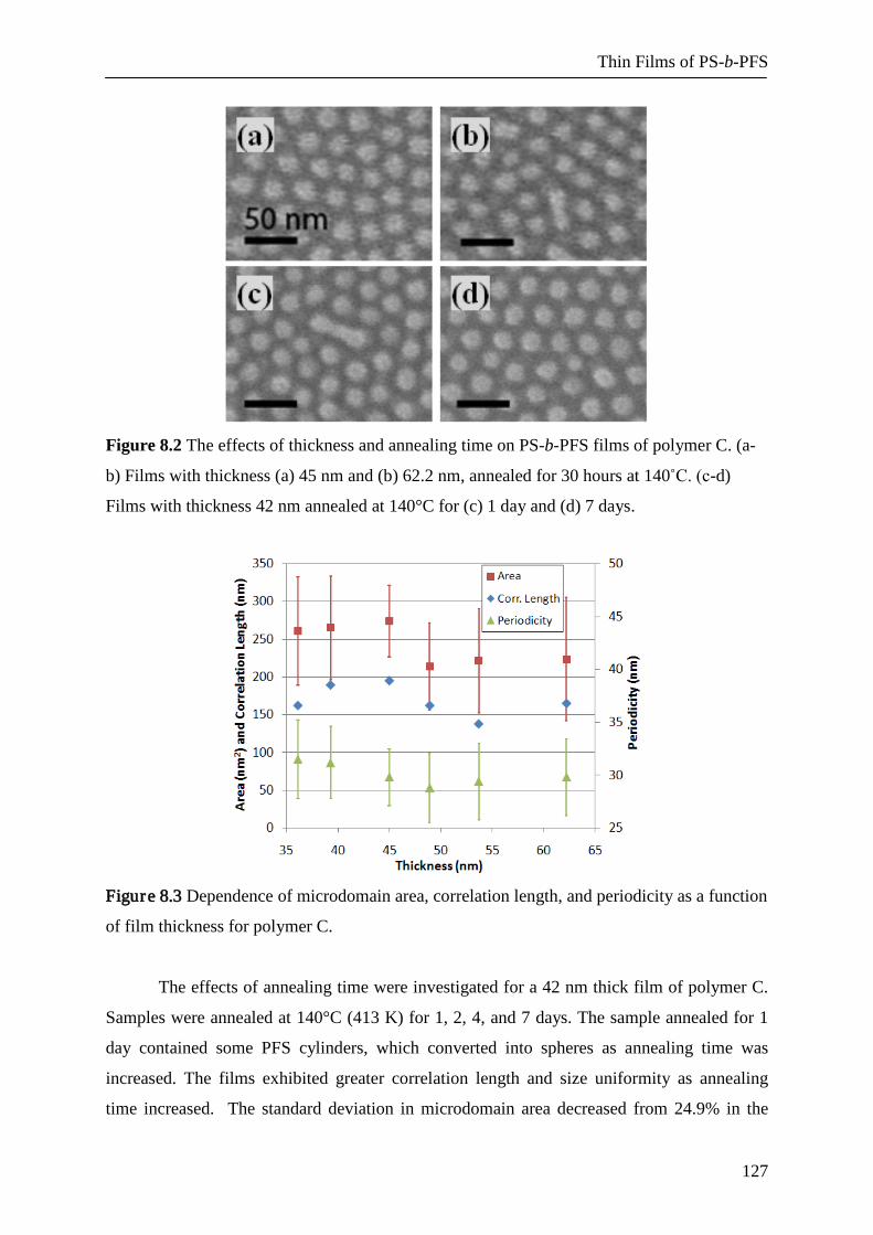
Thin Films of PS-b-PFS
127
Figure 8.2 The effects of thickness and annealing time on PS-b-PFS films of polymer C. (a-
b) Films with thickness (a) 45 nm and (b) 62.2 nm, annealed for 30 hours at 140˚C. (c-d)
Films with thickness 42 nm annealed at 140°C for (c) 1 day and (d) 7 days.
Figure 8.3 Dependence of microdomain area, correlation length, and periodicity as a function
of film thickness for polymer C.
The effects of annealing time were investigated for a 42 nm thick film of polymer C.
Samples were annealed at 140°C (413 K) for 1, 2, 4, and 7 days. The sample annealed for 1
day contained some PFS cylinders, which converted into spheres as annealing time was
increased. The films exhibited greater correlation length and size uniformity as annealing
time increased. The standard deviation in microdomain area decreased from 24.9% in the

Chapter 8
128
sample annealed for 1 day to 16.1% in the sample annealed for 7 days, while the standard
deviation in the microdomain period decreased from 32.2% to 8.7% and the correlation
length increased from 135 to 198 nm. Correlation length has been found to increase slowly
with annealing time by a power law 4/1)( tt ∝ξ for spherical-morphology PS-b-PI under
thermal annealing.[25] In our experiment, the correlation length after 2 days of annealing was
similar to that after 7 days annealing, so an annealing time of 30 h was chosen for subsequent
experiments.
8.2.3 Volume Fraction and Molecular Weight Effects
Figure 8.4 shows the morphology of etched 42 nm thick films of the five polymers
after 30 h annealing at 140̊ C. Although these polymers differ in their PFS volume fraction,
PDI and total molecular weight, the morphologies correlate most clearly with volume fraction
ФPFS. At low volume fractions (sample A: ФPFS = 13%), the PFS microdomains are small and
irregular. At mid-range volume fractions (samples B, C: ФPFS = 17-19%), the PFS
microdomains form uniform spheres, but at higher volume fractions (samples D, E: ФPFS =
20-22%), short PFS cylinders and spheres form simultaneously. The sphere-to-cylinder
transition occurring at ФPFS= 20% is similar to results from previous work.[4, 26] Table 8.2
gives the distributions in microdomain area and period and the correlation length for the five
polymers. The microdomain area (and its standard deviation) and period both increase with
ФPFS.
Figure 8.4 (a-e) PS-b-PFS films with thickness 42 nm, annealed for 30 hours, from polymers
A – E, respectively. (f) A pair density function (PDF) for image C.

Thin Films of PS-b-PFS
129
Table 8.2 Properties of five PS/PFS films with thickness of 42 nm, annealed for 30 hours.
Sample Area(nm2) Period(nm) ξ
Mean Std. Dev. Mean Std. Dev (nm)
A 117.8 47.3 22.7 4.5 120
B 222.5 47.7 26.4 2.9 141
C 249.8 44.9 29.5 3.1 171
D 290.7 104.9 29.0 3.3 195
E 447.1 381.2 30.3 3.2 135
The sphere-to-cylinder (S/C) and order/disorder (O/D) transitions may be predicted
from χN, with N the degree of polymerization and χ the Flory-Huggins interaction parameter.
For the PS-b-PFS system, χ is given by:
TTPFSPS /28.3028.0)(/ +=χ [27]
At an annealing temperature of 413 K and the average N-value of 419.7, χN = 15.1. The χN
vs. Ф phase diagram for the ideal behavior of a polystyrene-polyisoprene block copolymer[1]
predicts an O/D transition at Ф = 27% and S/C transition at Ф = 37%. In this experiment,
microphase separation clearly occurs for ФPFS = 13%, with a χN-value of 15.5, and the S/C
transition occurs near ФPFS = 22%, with a χN-value of 13.7. The phase diagram of PS-b-PFS
diblock-homopolymer blends is shown to be asymmetric which explains the shift in O/D
transition.[28]
No clear trends in microdomain area, period and correlation length with molecular
weight could be identified in this series of samples because of the overriding effects of
volume fraction. An increase in microdomain diameter and period with M2/3 is expected in
the strong segregation limit.[29] Comparing polymers B (ФPFS = 17%, M = 48.3 kg/mol) and C
(ФPFS = 19%, M = 54.1 kg/mol), both in the spherical regime without cylinders present, the
period increases by 1.12 (with standard deviation 10%), similar to the ratio (MC/MB)2/3 =
1.08. The ratio of PFS microdomain diameters is 1.06 (standard deviation 18%), but this is at
least partly due to the 5% increase in ФPFS.
8.2.4 Polydispersity Effect (PDI)
The PDI, defined as Mw/Mn, where Mw is the weight average and Mn the number
average molecular weight is of particular interest because it may determine the ultimate
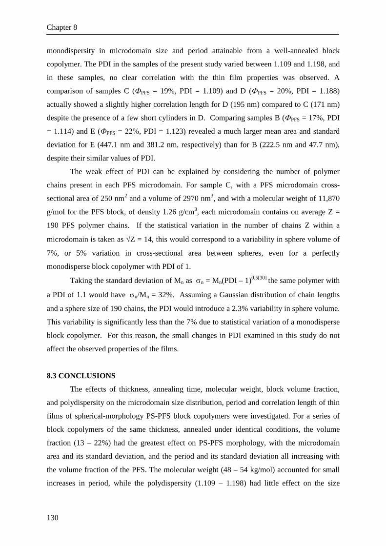
Chapter 8
130
monodispersity in microdomain size and period attainable from a well-annealed block
copolymer. The PDI in the samples of the present study varied between 1.109 and 1.198, and
in these samples, no clear correlation with the thin film properties was observed. A
comparison of samples C (ФPFS = 19%, PDI = 1.109) and D (ФPFS = 20%, PDI = 1.188)
actually showed a slightly higher correlation length for D (195 nm) compared to C (171 nm)
despite the presence of a few short cylinders in D. Comparing samples B (ФPFS = 17%, PDI
= 1.114) and E (ФPFS = 22%, PDI = 1.123) revealed a much larger mean area and standard
deviation for E (447.1 nm and 381.2 nm, respectively) than for B (222.5 nm and 47.7 nm),
despite their similar values of PDI.
The weak effect of PDI can be explained by considering the number of polymer
chains present in each PFS microdomain. For sample C, with a PFS microdomain cross-
sectional area of 250 nm2 and a volume of 2970 nm3, and with a molecular weight of 11,870
g/mol for the PFS block, of density 1.26 g/cm3, each microdomain contains on average Z =
190 PFS polymer chains. If the statistical variation in the number of chains Z within a
microdomain is taken as √Z = 14, this would correspond to a variability in sphere volume of
7%, or 5% variation in cross-sectional area between spheres, even for a perfectly
monodisperse block copolymer with PDI of 1.
Taking the standard deviation of Mn as σn = Mn(PDI – 1)0.5[30] the same polymer with
a PDI of 1.1 would have σn/Mn = 32%. Assuming a Gaussian distribution of chain lengths
and a sphere size of 190 chains, the PDI would introduce a 2.3% variability in sphere volume.
This variability is significantly less than the 7% due to statistical variation of a monodisperse
block copolymer. For this reason, the small changes in PDI examined in this study do not
affect the observed properties of the films.
8.3 CONCLUSIONS
The effects of thickness, annealing time, molecular weight, block volume fraction,
and polydispersity on the microdomain size distribution, period and correlation length of thin
films of spherical-morphology PS-PFS block copolymers were investigated. For a series of
block copolymers of the same thickness, annealed under identical conditions, the volume
fraction (13 – 22%) had the greatest effect on PS-PFS morphology, with the microdomain
area and its standard deviation, and the period and its standard deviation all increasing with
the volume fraction of the PFS. The molecular weight (48 – 54 kg/mol) accounted for small
increases in period, while the polydispersity (1.109 – 1.198) had little effect on the size

Thin Films of PS-b-PFS
131
distribution and period of the microdomains. The minor effects of PDI are attributed to the
large number of chains present in each microdomain.
Block copolymers containing an organic and an organometallic block are of interest
for self-assembled lithography because of the high etch selectivity between the blocks and the
high etch resistance of the organometallic block. The results of this study have implications
in the design of block copolymers for lithographic applications, such as the fabrication of
patterned magnetic recording media, where variation in the size and spacing of the
microdomains would produce a distribution of magnetic bit sizes and positions, leading to
increased noise in the readback signal.
8.4 EXPERIMENTAL
Poly(styrene-block-ferrocenyldimethylsilane) copolymers were synthesized by
sequential anionic polymerization. N,N,N',N',-Tetramethylethylenediamine (TMEDA),
ferrocene, styrene, n-butyllithium (1.6 M in hexanes), dibutylmagnesium (1.0 M in heptane)
and dichlorodimethylsilane were purchased from Aldrich. [1]Dimethylsilaferrocenophane
was prepared as described earlier and was purified by sequential crystallization and vacuum
sublimation cycles.[18, 31] Crystallizations was performed at low temperature in n-heptane.
Solutions of styrene in ethylbenzene were dried on dibutylmagnesium and distilled under
vacuum. n-Butyllithium was diluted to 0.2 M with n-heptane, which was dried over n-
butyllithium and distilled under vacuum. Tetrahydrofuran (THF) for anionic polymerization
was distilled from sodium-benzophenone under argon, degassed in three freeze-pump-thaw
cycles, and distilled by vacuum condensation from n-butyllithium at low temperature.
Polymer synthesis was carried out in an Mbraun Labmaster 130 glovebox under an
atmosphere of prepurified nitrogen (<0.1 ppm of H2O). Polymerization of styrene in
ethylbenzene was initiated by n-butyllithium and stirred for 5 hours at room temperature.
After the styrene block formation was completed, [1]-dimethylsilaferrocenophane was added
to the solution followed by some THF, allowing the formation of the organometallic block.
After 2 hours, the living chains were terminated by adding a few drops of degassed methanol.
The polymers were precipitated in methanol and dried under vacuum. Five different
copolymers were prepared by adding the required amount of initiator in several portions at
different time intervals, rather than at once.
The polymers were characterized by gel permeation chromatography (GPC) and 1H
NMR spectrometry. GPC measurements were carried out in THF using Waters™
microstyragel columns with pore sizes of 105, 104, 103 Å and a 500 Å guard column (Waters).

Chapter 8
132
The instrument was equipped with a dual detection system consisting of a differential
refractometer (Waters model 410) and a viscometer (Viscotek model H502). Molar masses
were determined relative to narrow polystyrene standards. 1H NMR spectra were recorded on
a Varian Unity Inova (300 MHz) instrument at 300.3 MHz in deuterated chloroform. Block
ratios were calculated from 1H NMR peak integrals. The density of
poly(ferrocenyldimethylsilane), 1.26 g/cm3, was obtained using a pycnometer. The properties
of the polymers are summarized in Table 8.1.
Solutions of the polymers in toluene (1.5 wt%) were spin coated onto prime silicon to
form films with thicknesses between 32 and 63 nm. Samples were annealed in a vacuum
furnace at 140 °C (413 K) for 1 to 7 days. The films were then reactive ion etched (RIE) in
oxygen for 25 seconds at 90W, which removed the PS and partly oxidized the PFS [27].
Samples were imaged using scanning electron microscopy (SEM) after etching, and
the images were analyzed using SigmaScan imaging processing and MATLAB software. The
areas and coordinates of the PFS microdomains were recorded, and MATLAB scripts were
used to calculate the size distribution and the pair density function (PDF). The PDF, g(r), is a
dimensionless measure of the density of objects around a point, and is defined as
),(),(1)(
drrrdAdrrrdnrg
++
=ρ
where ρ is the areal particle density, dn is the number of pairs of particles between a radial
distance r and r + dr, and dA is the area contained between r and r + dr. The correlation
length, ξ, was defined as the distance at which the amplitude of the PDF oscillations fell
below 5% of the peak amplitude. Correlation length is a measure of the order in a system.
8.5 ACKNOWLEDGEMENTS We thank Mr. Clemens Padberg for performing GPC analysis. 8.6 REFERENCES [1] F. S. Bates, G. H. Fredrickson, Annu. Rev. Phys. Chem. 1990, 41, 525.
[2] M. Park, C. Harrison, P. M. Chaikin, R. A. Register, D. H. Adamson, Science 1997,
276, 1401.
[3] K. Asakawa, T. Hiraoka, Jpn. J. Appl. Phys. 2002, 41, 6112.
[4] J. Y. Cheng, C. A. Ross, V. Z. H. Chan, E. L. Thomas, R. G. H. Lammertink, G. J.
Vancso, Adv. Mater. 2001, 13, 1174.
Thin Films of PS-b-PFS
133
[5] S. J. Jeong, G. D. Xia, B. H. Kim, D. O. Shin, S. H. Kwon, S. W. Kang, S. O. Kim,
Adv. Mater. 2008, 20, 1898.
[6] C. Park, J. Yoon, E. L. Thomas, Polymer 2003, 44, 6725.
[7] I. W. Hamley, Nanotechnology 2003, 14, R39.
[8] G. Krausch, R. Magerle, Adv. Mater. 2002, 14, 1579.
[9] M. Lazzari, M. A. Lopez-Quintela, Adv. Mater. 2003, 15, 1583.
[10] R. A. Segalman, Mater. Sci. Eng. Rep. 2005, 48, 191.
[11] J. Y. Cheng, C. A. Ross, H. I. Smith, E. L. Thomas, Adv. Mater. 2006, 18, 2505.
[12] S. B. Darling, Prog. Polymer Sci. 2007, 32, 1152.
[13] K. Naito, H. Hieda, M. Sakurai, Y. Kamata, K. Asakawa, IEEE Trans. Magn. 2002,
38, 1949.
[14] C. C. Liu, P. F. Nealey, Y. H. Ting, A. E. Wendt, J. Vac. Sci. Technol. B 2007, 25,
1963.
[15] T. Thurn-Albrecht, J. Schotter, C. A. Kastle, N. Emley, T. Shibauchi, L. Krusin-
Elbaum, K. Guarini, C. T. Black, M. T. Tuominen, T. P. Russell, Science 2000, 290,
2126.
[16] R. G. H. Lammertink, M. A. Hempenius, J. E. van den Enk, V. Z. H. Chan, E. L.
Thomas, G. J. Vancso, Adv. Mater. 2000, 12, 98.
[17] R. G. H. Lammertink, M. A. Hempenius, V. Z. H. Chan, E. L. Thomas, G. J. Vancso,
Chem. Mater. 2001, 13, 429.
[18] Y. Z. Ni, R. Rulkens, I. Manners, J. Am. Chem. Soc. 1996, 118, 4102.
[19] J. Y. Cheng, C. A. Ross, E. L. Thomas, H. I. Smith, G. J. Vancso, Adv. Mater. 2003,
15, 1599.
[20] Y. S. Jung, C. A. Ross, Nano Lett. 2007, 7, 2046.
[21] I. Bita, J. K. W. Yang, Y. S. Jung, C. A. Ross, E. L. Thomas, K. K. Berggren, Science
2008, 321, 939.
[22] S. G. Xiao, X. M. Yang, J. Vac. Sci. Technol. B 2007, 25, 1953.
[23] K. W. Guarini, C. T. Black, S. H. I. Yeuing, Adv. Mater. 2002, 14, 1290.
[24] M. Albrecht, C. T. Rettner, A. Moser, M. E. Best, B. D. Terris, Appl. Phys. Lett. 2002,
81, 2875.
[25] C. Harrison, D. E. Angelescu, M. Trawick, Z. D. Cheng, D. A. Huse, P. M. Chaikin,
D. A. Vega, J. M. Sebastian, R. A. Register, D. H. Adamson, Europhys. Lett. 2004,
67, 800.
Chapter 8
134
[26] R. G. H. Lammertink, M. A. Hempenius, E. L. Thomas, G. J. Vancso, J. Poly. Sci.
Poly. Phys. 1999, 37, 1009.
[27] H. B. Eitouni, N. P. Balsara, H. Hahn, J. A. Pople, M. A. Hempenius,
Macromolecules 2002, 35, 7765.
[28] R. G. H. Lammertink, M. A. Hempenius, E. L. Thomas, G. J. Vancso, J. Polym. Sci.
Part B, Polym. Phys. 1999, 37, 1009.
[29] T. Hashimoto, M. Shibayama, H. Kawai, Macromolecules 1980, 13, 1237.
[30] S. S. Rane, P. Choi, Chem. Mater. 2005, 17, 926.
[31] R. G. H. Lammertink, M. A. Hempenius, E. L. Thomas, G. J. Vancso, J. Polym. Sci.,
Polym. Phys. Ed. 1999, 37, 1009.

Summary and Outlook
The main goal pursued in this thesis is to investigate the role of organometallic
polymers in bottom-up and top-down nanofabrication techniques to provide patterned
platforms. Poly(ferrocenylsilane)s (PFSs) were explored for their use in top-down fabrication
since they show a high etch resistance to reactive ion etching (RIE). The PFS polymers
synthesized were used as resists in top-down lithographic applications on the micro- and
nanometer scales. Phase separation in block copolymers was used to create bottom-up
patterns on a nanometer scale. Surface-initiated polymerization (SIP) was performed for the
preparation of polymer brush patterns for use in biological applications.
Different lithography techniques such as nanoimprint lithography (NIL), UV-
nanoimprint lithography (UV-NIL) and nanosphere lithography (NSL) were employed to
fabricate patterns of PFS. The patterns fabricated were further utilized to create structures on
various polymer and silicon surfaces at different lengthscales. In addition, nanostructured
polymer brushes were grafted from a patterned initiator obtained by the step-and-flash
imprint lithography (SFIL) process. Block copolymer self-assembly was also used to generate
nanoperiodic PFS patterns. Symmetry, pattern quality and correlation as a function of the
primary structure of polystyrene-block-poly(ferrocenyldimethylsilane) (PS-b-PFS) is
discussed.
Chapter 1 provides a general introduction to this thesis. In Chapter 2, a broad
overview on existing lithography techniques and materials used in these techniques have been
given.
Chapter 3 presents a method to fabricate porous structures on silicon substrates by
using colloidal particle arrays as a template and PFS as an etch mask. Pores in silicon
substrates with submicron sizes and hcp order were fabricated by nanosphere lithography.
Silica nanoparticles of different sizes were used as starting materials and
poly(ferrocenylmethylphenylsilane) (PFMPS) as an etch-resistant polymer to produce a
negative replica of the nanoparticle array. The patterned silicon substrate was subsequently
used as a master to replicate the nanoparticle array by using NIL. The size of the pores in the
silicon substrate was controlled by changing the size of the particles. It was also shown that
the size and shape of the pores can be controlled by changing the etching time.

Summary
136
Chapter 4 describes a process to obtain free-standing poly(ethersulfone) (PES) films
exhibiting regular arrays of circular holes with a high porosity. The combination of NSL
lithography and a mask transfer technique used in this process allows the fabrication of
uniform, nanoporous PES membranes. RIE resistant poly(ferrocenylmethylphenylsilane)
(PFMPS) was used to fill the pores among the tightly packed silica particles. During pattern
transfer of the silica spheres to the PES, the top layer of PFMPS was removed first, exposing
the unprotected silica spheres. Following removal of the spheres by HF, a negative (hollow)
pattern of the colloidal particles was formed in the PFMPS layer. In RIE, the PES film was
perforated in unprotected areas corresponding to transfer of the projection pattern of the silica
spheres. Detachment of the PES membrane from the substrate was achieved by dissolving the
sacrificial CA layer in acetone. The PES membranes exhibiting dense, highly ordered pores
can serve as a platform for size-selective filtration of particles.
The application of PFMPS as a resist in nanoimprint lithography is introduced in
Chapter 5. Stable, homogeneous high molar mass PFMPS films obtained by spin coating
were imprinted and the resulting patterns were further transferred into the substrate by
reactive ion etching. Decreasing the initial film thickness and tuning the reactive ion etching
conditions facilitated the residual layer removal and improved the pattern transfer. In order to
obtain high aspect ratios, the residual layer was completely removed by Ar sputtering since
direct etching without removal of the residual layer gave rise to oxide layer formation, which
prevented further pattern transfer. Overall, it was shown that PFMPS, because of its excellent
etch contrast vs silicon, can be used as a single step resist since there is no need for metal lift-
off, which renders this approach a low-cost and potentially high-throughput process.
Chapter 6 describes the development of a UV-NIL process with a bilayer system, one
of which is PFMPS. The organometallic polymer PFMPS was spin-coated onto a UV-NIL
patterned substrate, followed by an argon plasma treatment to expose the imprint material.
Removal of the imprint material with oxygen plasma gave rise to PFMPS patterns forming a
negative replica of the template employed. Pattern transfer into silicon substrates was
accomplished by the use of a CHF3/SF6/O2 plasma. Variations of the plasma composition led
to different etch profiles. The fabrication of polymeric structures with lateral dimensions
down to 30 nm and aspect ratios of up to 3 was demonstrated. This process offers the
possibility for combining the advantages of UV-NIL with the high etch resistance of
poly(ferrocenylsilanes) to produce feature sizes down to the sub-100 nm range.
In Chapter 7 the preparation of polymer brush patterns by combining SFIL and SIP
techniques is reported. Patterns created by SFIL were further used for anchoring SAMs of an

Summary
137
initiator for performing SIP. The method allowed for the creation of brush patterns of
PEGMA, PS and PGMA, with sizes from several microns down to 40 nm. Such variation in
domain size enabled the study of the effect of the pattern size on the polymer brush height. It
was shown that nanosize domains exhibit a significantly reduced height. Several interesting
perspectives of patterned PEGMA brushes were demonstrated. PEGMA hydroxy groups
were converted into carboxylic acid groups and the pH response of these functionalized
PEGMA layers was analyzed by varying the pH. The fabricated structurally robust and
functional patterned PEGMA polymeric nanostructures were used for protein immobilization.
Streptavidin/biotin were selectively coupled on the activated PEGMA brush patterns.
Chapter 8 deals with the synthesis and symmetry, pattern quality and correlation as a
function of the primary structure of PS-b-PFS block copolymers. The effects of thickness,
annealing time, molar mass, block volume fraction, and polydispersity on the microdomain
size distribution, period and correlation length of thin films of spherical-morphology PS-b-
PFS block copolymers were investigated. For a series of block copolymer films of the same
thickness, annealed under identical conditions, the volume fraction was found to have the
greatest effect on PS-b-PFS morphology, with the period and its standard deviation all
increasing with the volume fraction of the PFS. On the other hand polydispersity had little
effect on the size distribution and period of the microdomains.
Organometallic polymers are very attractive materials which could be further
explored for other possible applications in lithography. Further research on controlled
patterning of PFS block copolymers by means of UV-NIL lithography can be carried out to
study the influence of confinement on block copolymer assembly. In addition, PFS block
copolymers could be utilized to pattern polymer surfaces down to 20 nm by carefully
designing the processes like etching, annealing, and deposition of materials.
The results presented in Chapter 7 illustrate the fabrication of polymeric platforms
which were further used for protein immobilization. The same approach could be performed
for the covalent attachment of CdSe/ZnS nano-crystals at the brush chain ends. In this case,
the confinement and patterning of nano-crystals could be studied.
The results presented in this thesis show that polymers provide a variety of structures
and dimensions, when patterned by bottom-up and top-down micro- and nanofabrication
techniques. The incorporation of organometallic units into the main chain of polymers
improves the properties such as etch resistivity, and thus applicability of these
macromolecules. Metal-containing polymers are proven to have high etch-resistant properties
when applied in NIL, SFIL and NSL techniques. They appear to be valuable candidates for

Summary
138
developing new resists formulations. The fabricated structures by using these techniques
could be employed in areas such as data storage, microelectronics and bioelectronics.
Samenvatting
Het hoofddoel van dit proefschrift is om de rol van organometaalpolymeren in
“bottom-up”- en “top-down”-nanofabricagetechnieken voor het vervaardigen van
nanogestructureerde platforms te onderzoeken. Het gebruik van poly(ferrocenylsilanen)
(PFSs) voor “top-down”-fabricage werd bestudeerd vanwege de hoge weerstand van deze
polymeren in “reactive ion etching” (RIE) processen. De gesynthetiseerde PFS-polymeren
werden gebruikt als resists in top-down lithografische toepassingen op micrometer- en
nanometerschaal. Oppervlakte-geïnitieerde polymerisatie werd uitgevoerd voor de constructie
van polymere brush-patronen voor gebruik in biologische toepassingen.
Verschillende lithografische technieken zoals nanoimprint-lithografie (NIL), UV-
nanoimprint-lithografie (UV-NIL) en nanodeeltjes-lithografie (NSL) zijn gebruikt om PFS-
patronen te genereren. De gefabriceerde patronen zijn gebruikt om structuren op polymeer-
en siliciumoppervlakken aan te brengen op verschillende lengteschalen. Nanogestructureerde
polymere brushes werden gegroeid vanaf initiatoren, patroonsgewijs aangebracht door middel
van “step-and-flash” imprint-lithografie (SFIL). Blokcopolymeer zelf-assemblage werd ook
gebruikt voor het verkrijgen van PFS patronen op nanometerschaal. Symmetrie,
patroonkwaliteit en correlatielengte als functie van de primaire structuur van polystyreen-
block-poly(ferrocenyldimethylsilaan)- (PS-b-PFS-) blokcopolymeren worden besproken.
Hoofdstuk 1 geeft een algemene inleiding tot het proefschrift. In Hoofdstuk 2 wordt
een overzicht van bestaande lithografische technieken en bijbehorende materialen gegeven.
Hoofdstuk 3 beschrijft een methode om poreuze structuren op silicium-substraten te
fabriceren door gebruik te maken van geordende monolagen van colloidale deeltjes als mal
en PFS als etsmasker. Poriën in silicium-substraten met submicrometer afmetingen en hcp-
ordening werden vervaardigd door middel van NSL. Silica nanodeeltjes van verschillende
grootte werden gebruikt als uitgangsmateriaal en poly(ferrocenylmethylphenylsilaan)
(PFMPS) als etsresistent polymeer, zodat een negatieve replica van de nanodeeltjes-laag werd
geproduceerd. Het op deze wijze gestructureerde silicium-substraat werd vervolgens als mal
gebruikt om de nanodeeltjes-laag te vermenigvuldigen door middel van NIL. De poriegrootte
in de silicium-substraten kon worden gevarieerd door het veranderen van de deeltjesgrootte.
Samenvatting
140
Ook werd aangetoond dat de grootte en vorm van de poriën kan worden gestuurd door het
aanpassen van de etstijd.
Hoofdstuk 4 beschrijft een proces om vrijstaande, niet door een substraat gedragen
poly(ethersulfon)- (PES-) films met regelmatige structuren van cirkelvormige poriën en een
hoge porositeit te vormen. De combinatie van NSL en een patroonoverdrachts-techniek
gebruikt in dit proces maakte de fabricage van uniforme, nanoporeuze PES-membranen
mogelijk. Het etsbestendige PFMPS werd gebruikt om de poriën tussen de dichtgepakte
silica-deeltjes op te vullen. Tijdens de patroonoverdracht van de silica-deeltjes in PES werd
de toplaag van PFMPS eerst weggehaald, resulterend in deels onbeschermde silica-deeltjes.
Na verwijdering van de silica deeltjes met HF werd een negatief gaten-patroon van de
colloidale deeltjes gevormd in de PFMPS-laag. Tijdens RIE werd de PES-film geperforeerd
in de onbeschermde gebieden, wat leidde tot overdracht van het projectiepatroon van de
silica-deeltjes. Loshalen van het PES-membraan van het onderliggende substraat bleek
mogelijk door het oplossen van de tussenliggende cellulose-acetaat laag in aceton. De PES-
membranen met hun dichtgepakte, goed gedefiniëerde poriën kunnen worden gebruikt voor
de grootte-selectieve filtratie van deeltjes.
De toepassing van PFMPS als resist in nanoimprint-lithografie wordt geïntroduceerd
in Hoofdstuk 5. Stabiele, homogene, hoog molecuulgewicht PFMPS-films verkregen door
spin-coating werden geperst met NIL en de resulterende patronen werden overgebracht in het
substraat door RIE. Het verminderen van de oorspronkelijke filmdikte en het optimaliseren
van de RIE-omstandigheden vergemakkelijkten het verwijderen van de resterende resistlaag
en verbeterden zo de patroonoverdracht. Om hoge aspect verhoudingen te verkrijgen werd de
resterende resistlaag volledig verwijderd door Ar-sputtering omdat direct etsen zonder
verwijderen van de resterende resistlaag de vorming van een oxidelaag tot gevolg had
waardoor verdere patroonoverdracht werd verhinderd. Aangetoond werd dat PFMPS
vanwege het zeer hoge etscontrast met silicium kan worden gebruikt als eenstapsresist omdat
zogenaamde “metal lift-off” niet noodzakelijk is, waardoor deze aanpak als een goedkoop en
mogelijk hoog-volume-proces kan worden beschouwd.
Hoofdstuk 6 beschrijft de ontwikkeling van een UV-NIL-proces op basis van een bi-
laag-systeem, waarvan één laag bestaat uit PFMPS. Het organometaalpolymeer PFMPS werd
gespincoat op een door UV-NIL gestructureerd substraat, gevolgd door een argon-plasma-
behandeling om de imprintresistlaag bloot te leggen. Verwijdering van de imprintresist door
middel van een zuurstofplasma gaf PFMPS-patronen die een negatieve afdruk vormden van
de gebruikte mal. Patroonoverdracht in silicium-substraten werd gerealiseerd door gebruik te

Samenvatting
141
maken van een CHF3/SF6/O2-plasma. Variaties in de plasmasamenstelling leidde tot
verschillende etsprofielen. De fabricage van polymeerstructuren met laterale afmetingen tot
30 nm en aspect verhoudingen tot 3 werd aangetoond. Dit proces biedt de mogelijkhed om de
voordelen van UV-NIL te combineren met de hoge etsweerstand van poly(ferrocenylsilanen),
om zo structuren met afmetingen tot onder de 100 nm te fabriceren.
In Hoofdstuk 7 wordt de vorming van polymere brush-patronen door het combineren
van SFIL en SIP behandeld. Patronen gemaakt met SFIL werden gebruikt voor het hechten
van zelf-assemblerende monolagen van een initiator voor SIP. De methode maakte het
mogelijk om brush-patronen van PEGMA, PS en PGMA te vormen met afmetingen van
enkele micrometers tot 40 nm. Door deze variatie in domeingrootte kon de invloed van
patroonafmetingen op de hoogte van de polymeerbrushes worden bestudeerd. Verschillende
interessante aspecten van lateraal gestructureerde PEGMA-brushes werden aangetoond. De
hydroxy-groepen van de gevormde PEGMA-structuren werden omgezet in
carbonzuurgroepen en de pH-respons van deze gefunctionaliseerde PEGMA-structuren werd
bestudeerd door het variëren van de pH. De gefabriceerde, robuuste PEGMA-nanostructuren
werden gebruikt voor eiwithechting. Streptavidine/biotine werden selectief gekoppeld aan
geactiveerde PEGMA-brush-patronen.
Hoofdstuk 8 beschrijft de synthese en symmetrie, patroonkwaliteit en ordening in
dunne films als functie van de primaire structuur van PS-b-PFS-blokcopolymeren. De invloed
van filmdikte, “annealing” omstandigheden (tijd, temperatuur) voor optimale domeinvorming
en -ordening door fasescheiding van de PS- en PFS-blokken, moleculaire massa, blok-
volumefractie en polydispersiteit op de microdomein-grootteverdeling, -periodiciteit en -
correlatielengte van dunne films van PS-b-PFS-blokcopolymeren met bolvormige morfologie
werd onderzocht. Voor een serie blokcopolymere films van dezelfde dikte, “annealed” onder
dezelfde omstandigheden, bleek dat de volumefractie de grootste invloed had op de PS-b-
PFS-morfologie. De domeinafstand en standaarddeviatie namen toe met toenemende PFS-
volumefractie. Polydispersiteit bleek echter weinig invloed te hebben op de grootteverdeling
en domeinafstand van de microdomeinen.
Organometaalpolymeren zijn attractieve materialen die verder kunnen worden
onderzocht op hun toepasbaarheid in lithografie. Verder onderzoek aan de gecontroleerde
structurering van PFS-blokcopolymeren door middel van UV-NIL-lithografie kan worden
uitgevoerd om de invloed van ruimtelijke begrenzing op blokcopolymere zelf-assemblage te
bestuderen. Bovendien zouden PFS-blokcopolymeren gebruikt kunnen worden om

Samenvatting
142
polymeeroppervlakken te patroneren met structuren tot 20 nm door een zorgvuldige keuze
van procesparameters tijdens etsen, “annealing” en depositie van materialen.
De resultaten gepresenteerd in Hoofdstuk 7 illustreren de fabricage van
polymeerplatforms die vervolgens werden gebruikt voor eiwithechting. Dezelfde methode
zou gevolgd kunnen worden voor de covalente hechting van CdSe/ZnS-nanokristallen aan de
uiteinden van de brushes. In dit geval kan de ruimtelijke inperking en laterale structurering
van nanokristallen worden bestudeerd.
De resultaten uit dit proefschrift laten zien dat polymeren een reeks van structuren
met diverse afmetingen en chemische functionaliteiten op oppervlakken kunnen vormen
wanneer ze worden gestructureerd door bottom-up en top-down micro- en
nanofabricagetechnieken. Het aanbrengen van organometaaleenheden in de hoofdketen van
polymeren verbetert de eigenschappen zoals etsweerstand en daardoor de toepasbaarheid van
deze macromoleculen. Metaalbevattende polymeren hebben bewezen te beschikken over een
hoge etsweerstand bij hun toepassing in NIL-, SFIL- en NSL-processen. Deze polymeren
lijken waardevolle kandidaten te zijn voor de ontwikkeling van nieuwe resists. De door
middel van deze technieken gefabriceerde structuren kunnen worden toegepast in gebieden
zoals dataopslag, microelectronica en bioelectronica.

Acknowledgements When I first came to Enschede I had little idea how I would improve myself scientifically,
besides how much fun I would have in these four years. I finished my thesis finally, and I would like
to thank many people for their help and support in accomplishing this. I am very glad that now it is
time for me to write this part of the thesis.
First, I would like to thank one of my promoters and supervisors Prof. Jurriaan Huskens for
accepting me as a PhD student. Dear Jurriaan, I always had your support and trust during these four
years. You always believed me and you made me feel this when I needed it the most. That is why I
did not give up and kept going on. From our biweekly meeting, I have learnt so much from you. You
were always patient to me even when I was making the same mistakes while writing a manuscript.
You gave me enough freedom to collaborate and try the things that I wanted to do. These helped me
to be more independent researcher. I want to thank you for all your help, ideas, guidance, and patience
throughout this whole thesis. There are not enough words to explain my gratitude. Thank you very
much.
I would like to express my gratitude and appreciation to my second promoter Prof. Julius
Vancso. Thanks Julius for the opportunity you gave me to be part of the MTP group which has been a
pleasure both scientifically and personally. The scientific discussions we had, especially in the last
year, were very instructive and I really learnt a lot. I truly appreciate it. I wish that we had more of
these meetings which were very useful for me.
I owe my gratitude to my daily supervisor, Dr. Mark Hempenius. Dear Mark, thanks for all
your help in the lab. You taught me how to do synthesis and how to handle the things in the lab. You
were very patient and you always had time for me even though you were very busy. I felt very
confident to have you always there. I would also like to thank you for translating the summary into
Dutch.
I would like to thank Prof. David Reinhoudt for the meetings we had in the first year of my
PhD and for the scientific contributions. They were useful with lots of nice ideas. We also had nice
talks about life, food, travelling which I really enjoyed.
During these four years I had the chance to collaborate with many people, the results of
which are presented in this thesis. I owe my appreciation to Dr. Boris Vratzov for all his help he
provided to teach me the SFIL technique. You always had time for me to prepare the samples or for
discussions. We had many nice discussions which were very essential to obtain the results presented
in Chapters 6 and 7. I would like to thank Prof. Caroline Ross and Joy Perkinson from MIT for their
contribution to Chapter 8. I would like to thank Dr. Edmondo Benetti for introducing me to the world

Acknowledgements
144
of polymer brushes and for his participation in Chapter 7. Your help and advice during the last period
of this thesis were very essential, thank you very much Eddy. I really learnt a lot from you. My
appreciation also goes to Xiaofeng Sui for his help with Chapter 7. You are a good chemist Xiaofeng
and you are always willing to help. I would like to thank my other collaborators. Dr. Xing Yi Ling
and Dr. In Yee Phang for all their help, ideas and support for Chapters 3 and 4. My dear friends, it
was pleasure to work with you and without your help I could not have completed this part of the
work. A special thanks goes to Dr. Szczepan Zapotoczny for teaching me AFM and for always being
very friendly. Christiaan, thanks for helping me in the cleanroom and in the laboratory when I started
my PhD.
Dear Clemens, thank you very for all your help during these years. You are an amazing
person, always positive. You managed to solve all my problems related to computers, equipment, etc.
We had nice, long talks (the topic could be whatever). You were patient to listen me and even you
gave me wise advice. I appreciate your friendship. Thanks to Marcel and Richard for their technical
support. The secretaries of MnF/SMCT/MTP, Izabel, Gerardine, Genevieve, are also thanked for
taking care of all the administrative work. I thank you Pascal for going so carefully through my
concept thesis. I also spent some time doing SEM measurements. Dear Mark Smithers, thanks for
your help and contribution to the SEM images. I enjoyed our talks about life, family especially music
while doing measurements. I would like to thank all the people in the cleanroom and in particular to
Hans, Huib, Ite-Jan, Eddy, Rene and Peter for their technical support and patience.
During my PhD, I have had the opportunity to meet a lot of fantastic people. I would like to
thank those who made these four years an unforgettable period for me: Denis and Eddy, my dear
friends, thanks for being there always to listen me. Even though you find my problems very stupid, I
like to share them with you guys. You always managed to cheer me up with your humor Denis. You
are my drinking coach. You trained me so much that I could compete with you now (more vodka,
only strong alcohol). I really appreciate it. We have been through the stressful thesis writing time,
thanks for all the support. Eddy, after sometime, I could get used to your way of living and your way
of handling things. You were always around so I never felt alone. I am also very grateful for your
scientific help as well. You taught me a lot (brush synthesis and AFM). I really know what tip
imaging means now. We really shared a lot during this time. I really enjoyed drinking tea, having
dinners, getting drunk, dancing, and watching movies together with you guys. Denis and Eddy, it is
nice having you as friends. Dear Xing Yi and In Yee, after our trip to Istanbul we got closer. Since
then we had great time together (especially dinners :)) Xing Yi, it was pleasure to talk and to share
things with you. In yee, I really miss to have drinks with you and I was amazed how much you could
eat and drink. Martina and Slyvain, thanks very much for your hospitality in Bordeaux and all the nice
French food. Dear Mirko, I remember with a lot of pleasure our trip to Istanbul (always doner, kebap).
Please keep in touch. Henk, you are the best movie editor and director I have ever worked with. It was
so much fun to make a movie with you. Nuria, the kid, it was so nice to have you in the group. We

Acknowledgements
145
participated in all the Erasmus parties by your initiative. Thanks for keeping the contact and calling
me when I needed. Dear Francesca, now you are a doctor and I am very happy about it. We shared too
much lately, even the same flat. Thanks for this. I wish to visit you and Riccardo in Rome. Davide
(the most relaxed Italian) I had the best time in Lunteren when you were there with us. Carlo (the
grandpa), thanks for your hospitality in Munster (bed and breakfast). Kim, the most addictive friend
of mine to Turkish food. You are the most relaxed and easy going visitor that I had so far. Sorry that I
did not understand your English at the beginning. Do you remember our first weeks writing in the
same office but not talking? Now it is much fun to talk with you while taking tea, eating cookies and
of course drinking. Victoria, you are a very social person and, we were having lots of fun dancing
(non-stop). Nobody could replace you.
I would like to thank Bilge for her unconditional support during the last year of my PhD.
Thanks for cooking for me when I was working till late. You made sure that I was eating properly.
Thanks for all the good care. I am very happy to have you as a friend and I know that I can always
trust you. Another very good Turkish friend of mine, Deniz, thanks for waiting me in the lab when I
was working till late. You always have tea, cookies to share and of course tosties. You always tried to
cheer me up when I was down. I am sorry if I bothered you too much. I always feel relieved to talk
with you. And Oya, my alternative friend, you helped me a lot especially at the beginning when I was
very new in the group. During these years you always managed to surprise me (you know what I
mean) but I really enjoyed a lot with you especially while traveling (Venice, States, Barcelona).
Staying in the same room was always fun with you even though you were smoking. Cem, always
willing to help without asking anything back. Thanks for helping me when I was moving. You did not
complain at all (amazing). Erhan-Arzu, thanks for being there when I needed (especially for
maintenance of my bike and moving my stuff even twice). I wish that we had spent more time
together. I would also like to thank some people in TUSAT community; Kamil, Aysegul, Hasan,
Selim, Emre, Feridun, Anil (my dear japanish-turkish friend), Berk, Murat, Can (my dear dancing and
drinking friend), Burak (my ex-neighbor; thanks for everything during these years), Ayse, Ozlem,
Mustafa and Zeynep-Aytac.
With many people from outside of my groups I spent great times and we have nice memories.
Raffaella, Mauritzo, Giulia, Pietro, Nick, Stefano, Bob, Can, Laura, Anil, Cem, Bilge, David (the
great salsa-dancer, thank you for teaching me salsa), Roald (thanks for your advice for my future),
Burak, Lorenzo and Valeria. My dear friend Valeria, my best Italian flatmate ever. We shared the
same flat for two years without having any problem. I enjoyed having Turkish breakfast with you. We
had great time together. Even, you never complained about Denis and Eddy being there. You are a
very special person and I miss you a lot.
I would like to thank some people who left the group but I still keep in touch. Monique, you
were very friendly since the beginning. You were part of the PFS team. Thanks for helping me with
the synthesis and for all the lab work. Another member of PFS team: Thomas. It has been always

Acknowledgements
146
pleasure to go out with you (too much dancing). Thanks for visiting me in Istanbul and thanks for the
hospitality in Barcelona. Dear Marina and Melba, you were like my sisters. I appreciate your guidance
and support during your staying here. Miguel- Marina, thanks for everything when we visited you in
Barcelona. Enschede has never been the same after you left. Bas, Janina, Olga, Alessio, Fernando,
Lourdes, Riccardo and Olga (Turkish one) are also thanked for all the good times.
It is time to thank people from MTP/MnF and SMCT. Joost, I always enjoyed our
conversations about work, life, and relations. Lately, I even like your humor. You are very nice and
polite to help me with many paper work and with AFM related problems. Jealemy, you are a good
friend to have, I had a lot of fun doing our girly things. I don’t remember how many times we partied
lately. I will always remember the party in Atak (with many Russians). A special thanks to Albert for
being a great actor. Jing, my dear office-mate, thanks for listening to my complaints in the mornings.
You were always very patient with me even to my never ending AFM related questions. I hope I can
visit you in Singapore. Please don’t work there that much. Dear Jordi, you are a very sweet and nice
person. Please try to be happier and more positive. I know how hard it is here but you will manage.
Yiping, I enjoyed our talk in the cleanroom and you were always ready to help me when I needed.
Thanks for this. I would also like to thank to Shu-Han, Pieter, Duan, Carlo, Mudassir (thanks calling
me paradise), Lanti, Alberto, Melanie, Raluca, Vijay, Chien-Ching Wu, Dae June, Oktay, Edit, Anika,
Qi, Wilma, Gabriella, Mathijs, Nayeli, Gerwin, Anna, Maryana (always nice to see you in the lab or
in the cleanroom) and Mine. Dear Mine, we shared the same flat for a while. You were very
supportive and very nice to me. I really enjoyed our talks about work, people, and life.
All the people I mentioned here have contributed to make the time I spent in Enschede an
unforgettable time of my life. But most importantly, I owe my deepest gratitude to my family; my
parents, my two sisters and my brother for all the support they give me. Canim annecim ve babacim,
bana her zaman cok destek oldunuz. Her zaman ne istediysem yapmama izin verdiniz ve bana hep
guvendiniz. Maddi ve manevi tum desteginiz icin cok tesekkur ederim, sizi cok seviyorum. Canim
ablam Keti, sen her zaman, her seyimle ilgilendin. En ufak sorunuma yetistin. Cok saol ablacim, iyi ki
varsin. Krisim, bi tanem, biz seninle hep ikiz gibiydik. Her seyimizi paylastik, Beni en iyi taniyan kisi
de sensin, her zaman beni anladin. Bunca yil uzakta kalmis olsak da, hic kopmadik ve kopmayalim.
Biricik erkek kardesim Nasirim, sensiz bir yasam dusunemiyorum. Cok komiksin, cok tatlisin ama
biraz daha buyumen lazim. Canlarim siz benim herseyimsiniz.
Canet Acikgoz

About the Author Canet Acikgoz was born in 10th January, 1980 in Iskenderun, Turkey. She obtained her
bachelor degree of chemistry from Middle East Technical University (METU) in the year of
2003. She continued her master education in the same university and joined the group of
Prof. Dr. Metin Zora at METU. She received her master degree of Chemistry in August 2005,
with the research project entitled “The use of Fischer carbenes in the synthesis of
cycloheptadienones incorporating ferrocenyl moiety”. During these two years, she also
worked as a teaching assistant at Atilim University in Ankara. From January 2006, she has
been a PhD student under the supervision of Prof. Dr. Jurriaan Huskens and Prof. Dr. Julius
Vancso, in the Molecular Nanofabrication (MNF) and Material Science and Technology of
Polymers (MTP) groups at the University of Twente, on the use of polymers in bottom-up
and top-down micro-and nanofabrication techniques. The results of this research work are
described in this thesis