continous drain current rating and bonding wire · pdf filepower mosfet continuous drain...
TRANSCRIPT
Power MOSFET Continuous Drain current rating and Bonding wire limitation
Fei Wang , Kai Liu, Anup Bhalla
Abstract
Power MOSFET datasheets will usually show maximum values for continuous drain current Id, on the first page of datasheets.
For bottom exposed part such as DPAK, TO220, D2PAK, there is always a note besides Id rating saying that Id is limited by bonding wires. Is this true? The answer is no for most of the cases.
The reason would be shown in this article and more studies will be present to show, how low the silicon resistance should be to lead to a bonding wire limitation issue. Introduction
Power MOSFET maximum rating of Id is base on one of the following limitation, whichever limitation reaches first:
1. Thermal resistance limitation for transistor die and thermal runaway. 2. Bonding wire limitation
a. Wire fusion b. Thermal degradation of molding compound.
For packages with no bottom exposure, the heat sinking capability is limited from transistor die to PCB. Id is usually
limited by max junction temperature MOSFET can take. Because the usually low duty cycle real applications, to give a close to truth and meaningful current rating for power MOSFET, there is a convention in MOSFET business to rate the Id the non-bottom exposure devices by 10s Max Junction to Ambient thermal resistance:
(max)max)( @ JonDS
DD TR
PI =
For package with bottom exposure, heat sinking to PCB or heat sink can be maximized by properly circuit and heat
sink design. On datasheet for all these kind of MOSFET, Junction to Case thermal resistance will be used to calculate power dissipation PD. By doing so bonding wire limitation has to be taking account.
Physics of Id Limitations
A. Thermal Runaway
Power MOSFETs display increase of the on-resistance with temperature. Power dissipated in this resistance causes more heating of the junction, which further increases the junction temperature, in a positive feedback loop. (However, the increase of on-resistance with temperature helps balance current across multiple MOSFETs connected in parallel and current hogging does not occur). If the transistor produces more heat than the heat sink can dissipate, the thermal runaway happens and destroys the transistor. This problem can be alleviated to a degree by lowering the thermal resistance between the transistor die and the heatsink.
(max)
(max)
J
aJD R
TTP
Θ
−=
– 2 – May 21, 2009
AOS Copyrighted
B. Bonding wire limitation theory
The fire impression of bonding wire limitation is wire fusing. The whole MOSFET business calculates bonding wire limitation base on the wire fusing theory. We’ll discuss the validity of the implementation of this theory later.
The basic design equation for wire fuses is the Preece equation (W.H. Preece, Royal Soc. Proc., London, 36, p464, 1884) for wires in free air:
5.1DAI ×=
Where A=10244 for cupper/gold, A=7585 for aluminum. D is the diameter of wire in inches. However, nowadays most chips are encapsulated in plastic and conduction through the molding compound usually slows the temperature increase in the wire significantly, the existing formulas limit the allowable DC current too much. In case of transient loading, heat is also stored as internal energy in the molding compound. As a result, the wire will not become as warm as predicted by known formulas. In free air, wire current limited by melting temperature. In usual molding compounds decomposition occurs if temperature exceeds about 220 C. This temperature limit restricts the permissible current.
People modified the constant A for bonding wire limitation: 5.1DAI ×=
D = wire diameter in inches I = DC or rms current.
For bonding wires in plastic packages. A = 30000 for Gold or Copper with a bond-to-bond length <= 0.040 in. (0.1cm) A = 20500 for Gold or Copper with a bond-to-bond length >0.040 in. (0.1cm). A = 22000 for Aluminum with a bond-to-bond length <= 0.040 in. (0.1cm) A = 15200 for Aluminum with a bond-to-bond length >0.040 in. (0.1cm).
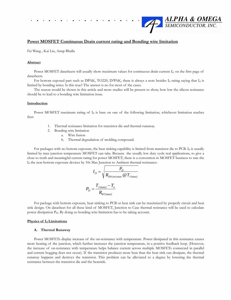
From this equation, we can derive the wire bonding limitation table we are using for datasheet:
Table 1: Bonding wire limitation for different wire materials and wire diameters, based on Modified Peece equation.
By doing simple calculation, it’s easy to find out most bottom exposed MOSFETs are bonding wire limited. Is this
true? To answer this question we run the electrical and thermal simulation for one of our D-PAK MOSFET AOD452 (Rds(on)=6.5mohm, Vgs=10V) with 2 x 12mils wire bonded on Source. Wire resistance is around 0.6mohm.
Merterial D(mils) I (A) <1mm I (A) >1mmCu/Au 1 0.9 0.6Cu/Au 1.3 1.4 1.0Cu/Au 1.5 1.7 1.2Cu/Au 2 2.7 1.8
Al 1 0.7 0.5Al 1.25 1.0 0.7Al 1.5 1.3 0.9Al 2 2.0 1.4Al 3 3.6 2.5Al 4 5.6 3.8Al 5 7.8 5.4Al 8 16 11Al 10 22 15Al 12 29 20Al 15 40 28Al 18 53 37Al 20 62 43
– 3 – May 21, 2009
AOS Copyrighted
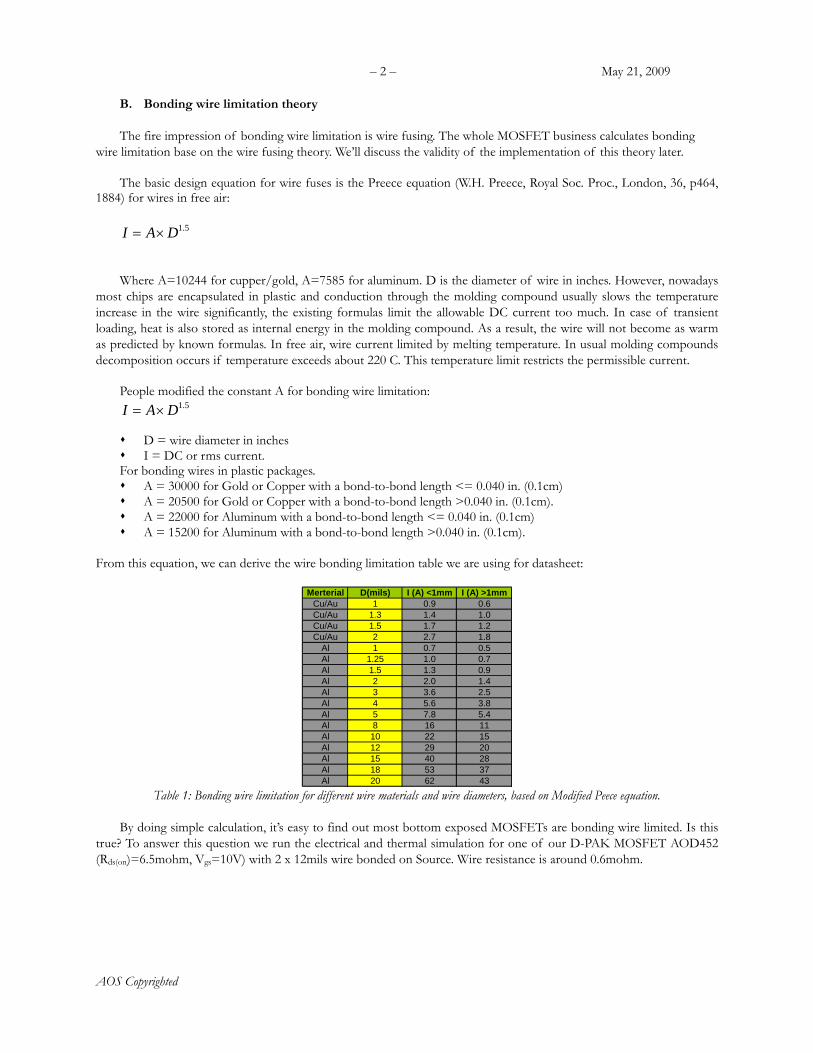
Figure 1: AOD452 (D-PAK) electrical simulation. Ohm loss in wire and transistor die are calculated Based on the result of electrical simulation in Fig 1, the thermal simulation results are followed. Two different cases
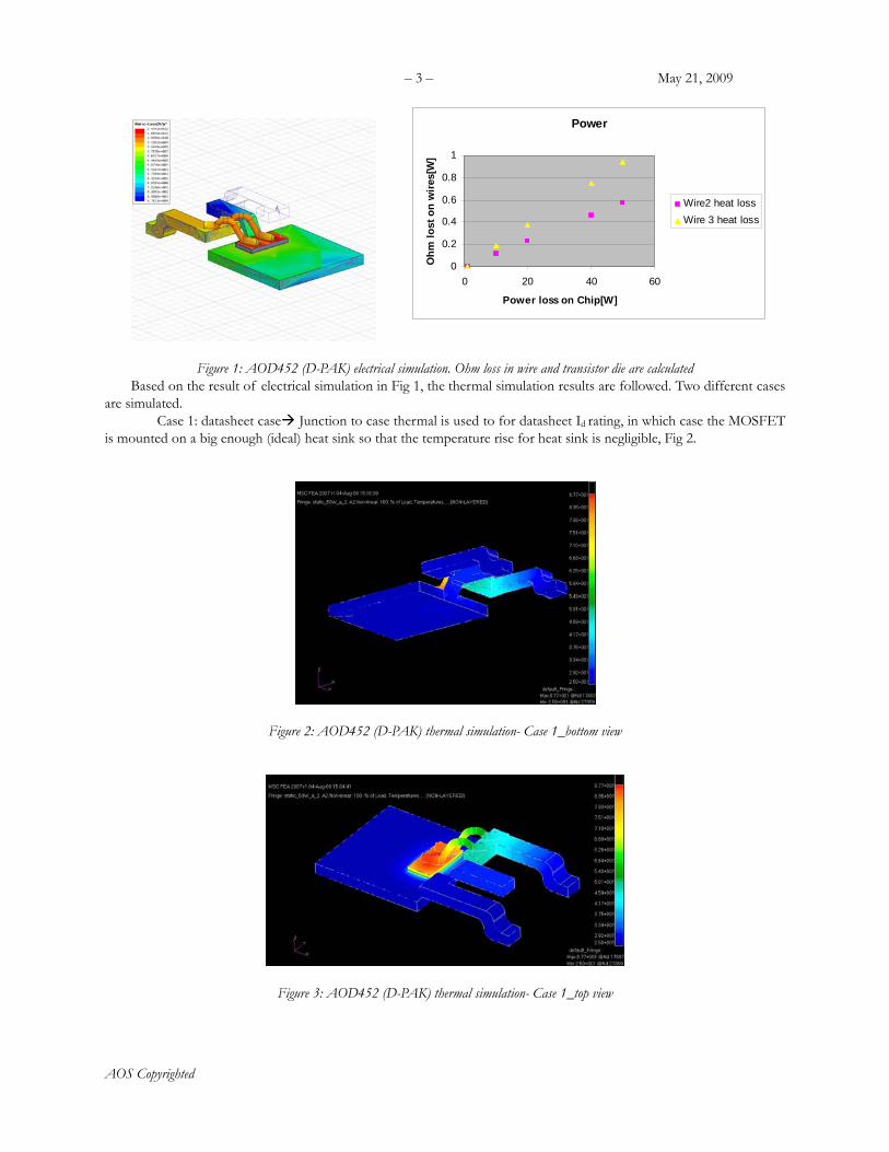
are simulated. Case 1: datasheet case Junction to case thermal is used to for datasheet Id rating, in which case the MOSFET
is mounted on a big enough (ideal) heat sink so that the temperature rise for heat sink is negligible, Fig 2.
Figure 2: AOD452 (D-PAK) thermal simulation- Case 1_bottom view
Figure 3: AOD452 (D-PAK) thermal simulation- Case 1_top view
Power
0
0.2
0.4
0.6
0.8
1
0 20 40 60
Power loss on Chip[W]
Ohm
lost
on
wire
s[W
]
Wire2 heat lossWire 3 heat loss

– 4 – May 21, 2009
AOS Copyrighted
Figure 4: AOD452 (D-PAK) thermal simulation- Case 1_wire view Heat distribution for this case is shown in Fig. 3 and Fig. 4. Because Rds(on) of MOSFET is more than 10 times wire resistance, more than 90% of total heat is generated by the die, even though the die attached to lead frame whose back side have ideal convection for heat releasing, the die surface, where wire bond landed, has the highest current density, therefore, is the hottest spot. These results are linear, which means Tjmax will always be firstly achieved
before the bonding wire would ever reach 220 ºC, namely, never there is a bonding wire limitation issue. A question may be raised that the wire temperature is low because it heat sink through source lead which also has ideal convection at the end. To answer this question we did another simulation (Case 2.) with all other conditions the same and remove ideal convection from source lead. The result is in Fig. 4 and Fig. 5. The hottest spot is still on the surface of the die. The only different is now almost all heat convection thru bottom exposure. Temperature gradient on source lead changed and absolute value on the die increased a little.
Figure 5: AOD452 (D-PAK) thermal simulation- Case 2_bottom view

– 5 – May 21, 2009
AOS Copyrighted
Figure 6: AOD452 (D-PAK) thermal simulation- Case 2_top view So far we know for the thermal condition we use on datasheet, which is use junction to case thermal to calculate maximum continuous drain current, there would be no bonding wire limitation issue. Datasheet condition is an ideal condition which gives us the maximum Id the MOSFET can get. In reality the MOSFET usually soldered on a finite size PCB with limited convection for heat releasing. Therefore we simulated the third case with MOSFET mounted on a 1 in2 1 oz. PCB in still air. All other conditions are the same. The results are shown in Fig.7 and Fig.8. Now the temperature gradient on lead frame appears and absolute temperature values are much higher due to finite convection. But the hottest spot is still on the surface of the die. Our previous conclusion still stands.
Figure 7: AOD452 (D-PAK) thermal simulation- Case 3_top view with molding compound
– 6 – May 21, 2009
AOS Copyrighted
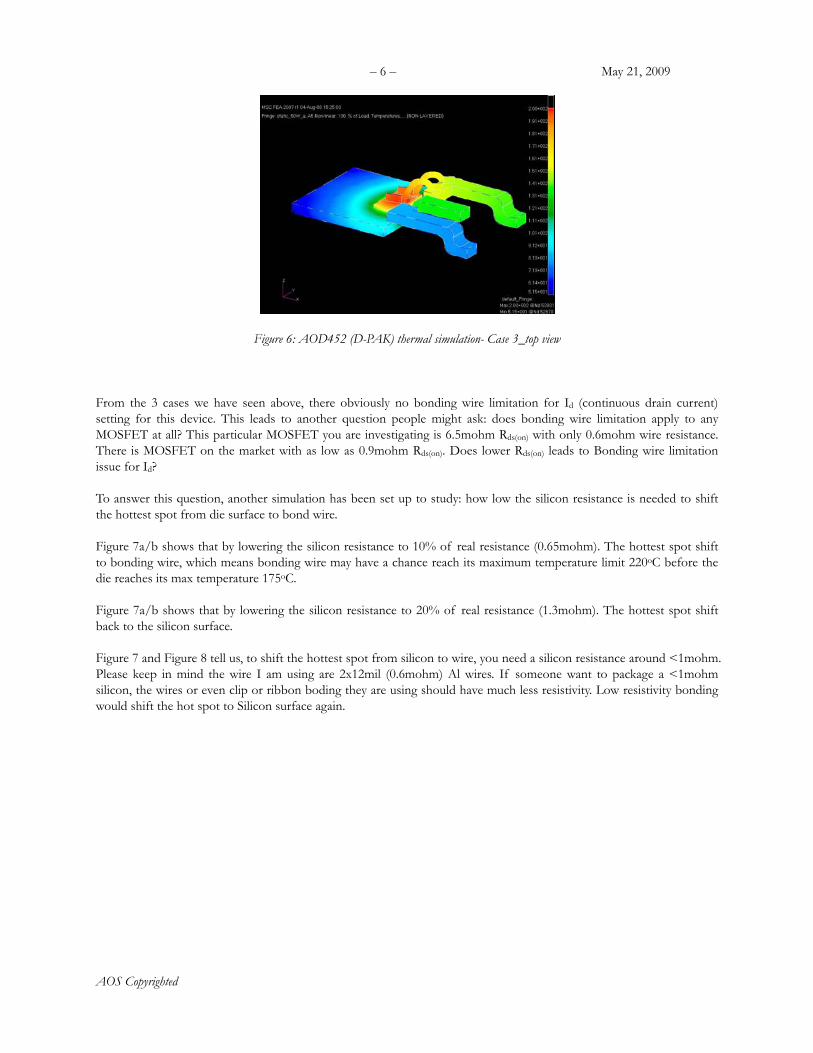
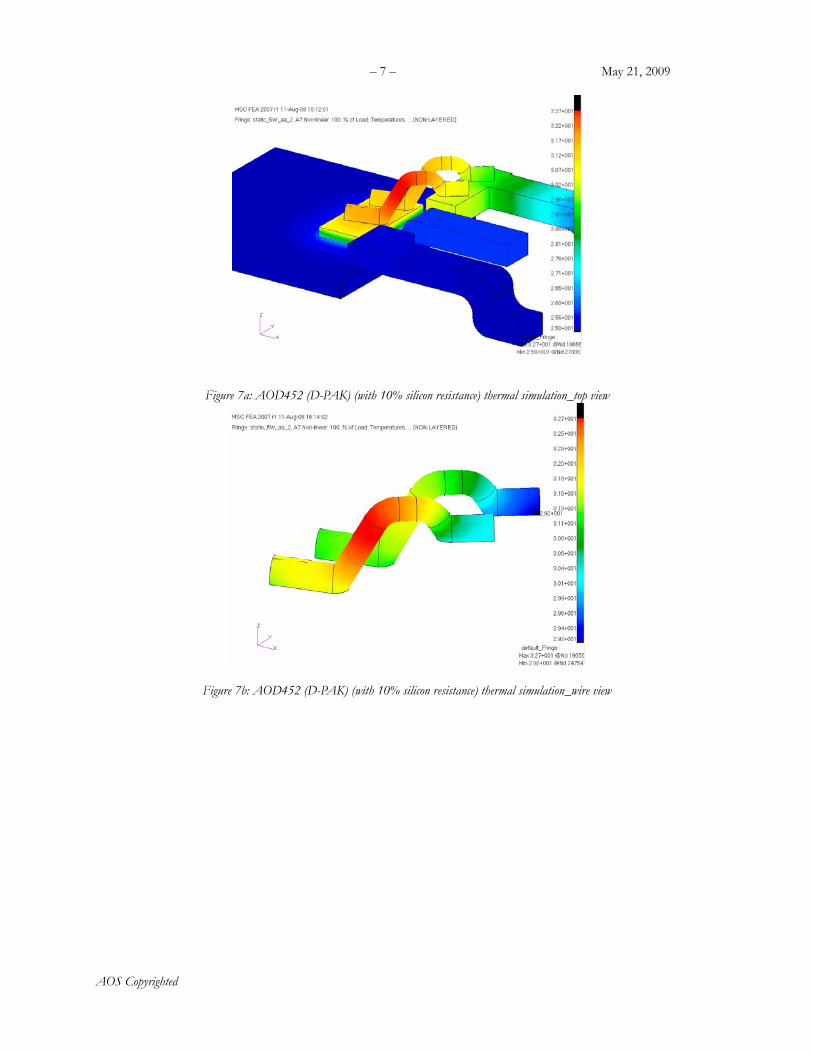
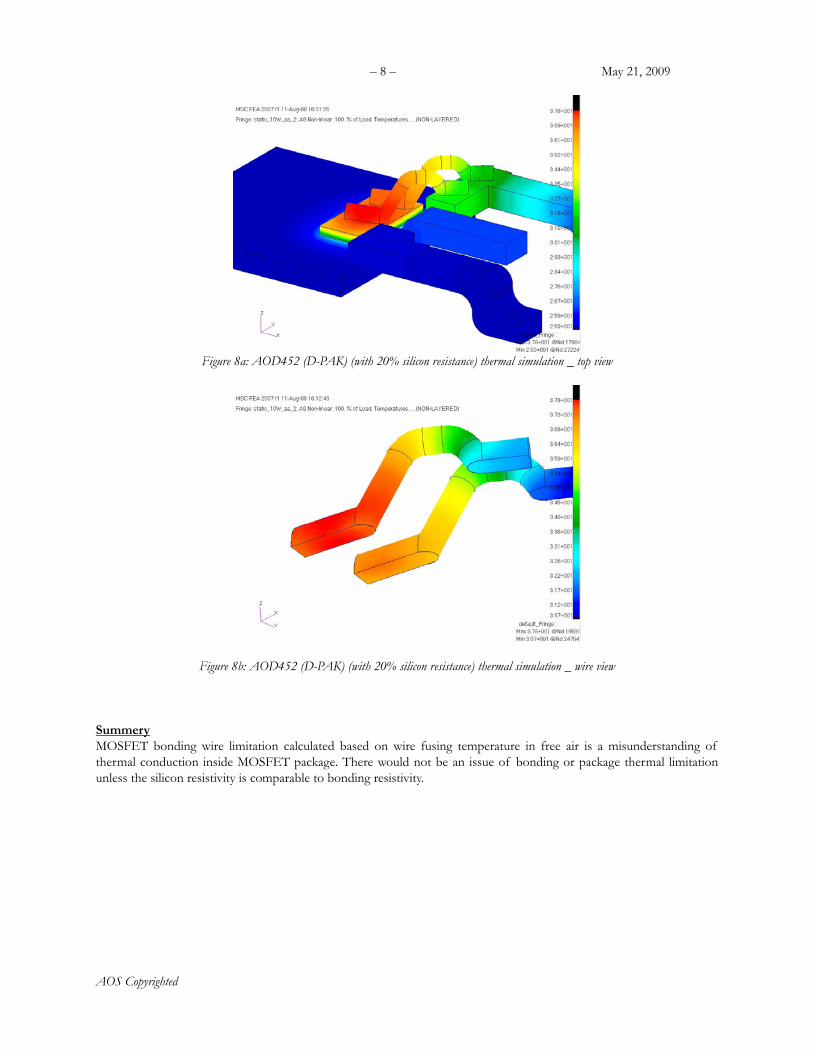
Figure 6: AOD452 (D-PAK) thermal simulation- Case 3_top view From the 3 cases we have seen above, there obviously no bonding wire limitation for Id (continuous drain current) setting for this device. This leads to another question people might ask: does bonding wire limitation apply to any MOSFET at all? This particular MOSFET you are investigating is 6.5mohm Rds(on) with only 0.6mohm wire resistance. There is MOSFET on the market with as low as 0.9mohm Rds(on). Does lower Rds(on) leads to Bonding wire limitation issue for Id? To answer this question, another simulation has been set up to study: how low the silicon resistance is needed to shift the hottest spot from die surface to bond wire. Figure 7a/b shows that by lowering the silicon resistance to 10% of real resistance (0.65mohm). The hottest spot shift to bonding wire, which means bonding wire may have a chance reach its maximum temperature limit 220oC before the die reaches its max temperature 175oC. Figure 7a/b shows that by lowering the silicon resistance to 20% of real resistance (1.3mohm). The hottest spot shift back to the silicon surface. Figure 7 and Figure 8 tell us, to shift the hottest spot from silicon to wire, you need a silicon resistance around <1mohm. Please keep in mind the wire I am using are 2x12mil (0.6mohm) Al wires. If someone want to package a <1mohm silicon, the wires or even clip or ribbon boding they are using should have much less resistivity. Low resistivity bonding would shift the hot spot to Silicon surface again.
– 7 – May 21, 2009
AOS Copyrighted
Figure 7a: AOD452 (D-PAK) (with 10% silicon resistance) thermal simulation_top view
Figure 7b: AOD452 (D-PAK) (with 10% silicon resistance) thermal simulation_wire view
– 8 – May 21, 2009
AOS Copyrighted
Figure 8a: AOD452 (D-PAK) (with 20% silicon resistance) thermal simulation _ top view
Figure 8b: AOD452 (D-PAK) (with 20% silicon resistance) thermal simulation _ wire view Summery MOSFET bonding wire limitation calculated based on wire fusing temperature in free air is a misunderstanding of thermal conduction inside MOSFET package. There would not be an issue of bonding or package thermal limitation unless the silicon resistivity is comparable to bonding resistivity.
– 9 – May 21, 2009
AOS Copyrighted
Revision History
Date Revision Changes 5/21/2009 1 Initial release
– 10 – May 21, 2009
AOS Copyrighted
Please Read Carefully:
Information in this document is provided solely in connection with AOS products. Alpha & Omega Semiconductor (“AOS”) reserve the right to make changes, corrections, modifications or improvements, to this document, and the products and services described herein at any time, without notice.
All AOS products are sold pursuant to AOS’s terms and conditions of sale. Purchasers are solely responsible for the choice, selection and use of the AOS products and services described herein, and AOS assumes no liability whatsoever relating to the choice, selection or use of the AOS products and services described herein. No license, express or implied to any intellectual property rights is granted under this document. If any part of this document refers to any third party products or services it shall not be deemed a license grant by AOS for the use of such third party products or services, or any intellectual property contained therein or considered as a warranty covering the use in any manner whatsoever of such third party products or services or any intellectual property contained therein. UNLESS OTHERWISE SET FORTH IN AOS’S TERMS AND CONDITIONS OF SALE AOS DISCLAIMS ANY EXPRESS OR IMPLIED WARRANTY WITH RESPECT TO THE USE AND/OR SALE OF AOS PRODUCTS INCLUDING WITHOUT LIMITATION IMPLIED WARRANTIES OF MERCHANTABILITY, FITNESS FOR A PARTICULAR PURPOSE (AND THEIR EQUIVALENTS UNDER THE LAWS OF ANY JURISDICTION), OR INFRINGEMENT OF ANY PATENT, COPYRIGHT OR OTHER INTELLECTUAL PROPERTY RIGHT. UNLESS EXPRESSLY APPROVED IN WRITING BY AN AUTHORIZED AOS REPRESENTATIVE, AOS PRODUCTS ARE NOT RECOMMENDED, AUTHORIZED OR WARRANTED FOR USE IN MILITARY, AIR CRAFT, SPACE, LIFE SAVING, OR LIFE USTAINING APPLICATIONS, NOR IN PRODUCTS OR SYSTEMS WHERE FAILURE OR MALFUNCTION MAY RESULT IN PERSONAL INJURY, DEATH, OR SEVERE PROPERTY OR ENVIRONMENTAL DAMAGE. Resale of AOS products with provisions different from the statements and/or technical features set forth in this document shall immediately void any warranty granted by AOS for the AOS product or service described herein and shall not create or extend in any manner whatsoever, any liability of AOS.
AOS and the AOS logo are trademarks or registered trademarks of AOS in various countries.
Information in this document supersedes and replaces all information previously supplied.
The AOS logo is a registered trademark of Alpha & Omega Semiconductor. All other names are the property of their respective owners.
© 2009 Alpha & Omega Semiconductor - All rights reserved