contents - hawaii preparatory...
TRANSCRIPT

24.1 A 100-W Compact Z-Match Antenna Tuner
24.2 A Microprocessor-Controlled SWR Monitor
24.3 A 160- and 80-M Matching Network for Your 43-Foot Vertical
24.4 Switching the Matching Network for Your 43-Foot Vertical
24.5 An External Automatic Antenna Switch for Use With Yaesu or ICOM Radios
24.6 A Low-Cost Remote Antenna Switch
24.7 Audible Antenna Bridge
24.8 A Trio of Transceiver/Computer Interfaces
24.9 A Simple Serial Interface
24.10 USB Interfaces For Your Ham Gear
24.11 The Universal Keying Adapter
24.12 The TiCK-4 — A Tiny CMOS Keyer
24.13 The ID-O-Matic Station Identification Timer
24.14 An Audio Intelligibility Enhancer
24.15 An Audio Interface Unit for Field Day and Contesting
Contents
Station Accessories 24.1
24.1 A 100-W Compact Z-Match Antenna Tuner
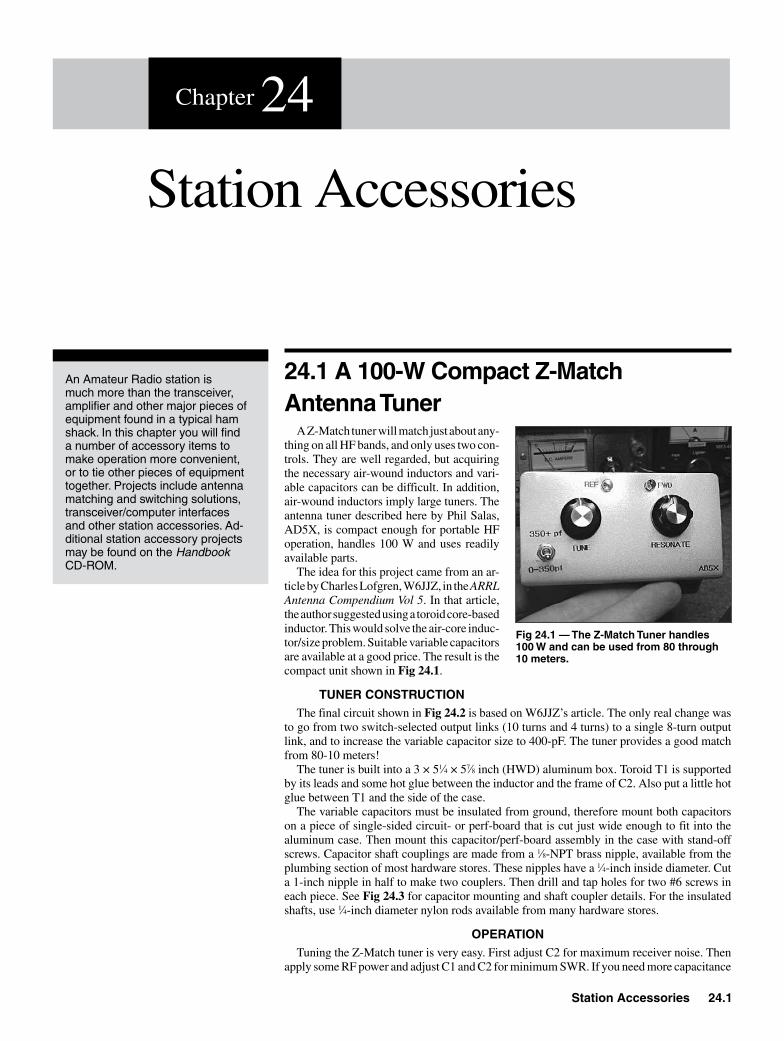
A Z-Match tuner will match just about any-thing on all HF bands, and only uses two con-trols. They are well regarded, but acquiring the necessary air-wound inductors and vari-able capacitors can be difficult. In addition, air-wound inductors imply large tuners. The antenna tuner described here by Phil Salas, AD5X, is compact enough for portable HF operation, handles 100 W and uses readily available parts.
The idea for this project came from an ar-ticle by Charles Lofgren, W6JJZ, in the ARRL Antenna Compendium Vol 5. In that article, the author suggested using a toroid core-based inductor. This would solve the air-core induc-tor/size problem. Suitable variable capacitors are available at a good price. The result is the compact unit shown in Fig 24.1.
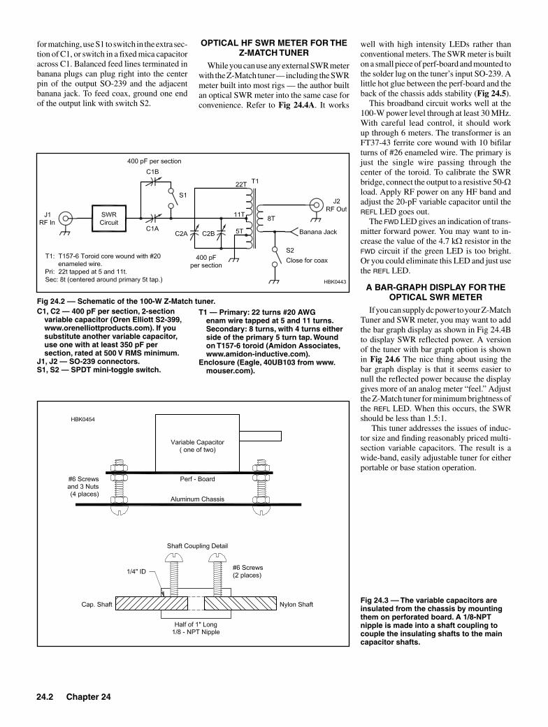
TUNER CONSTRUCTIONThe final circuit shown in Fig 24.2 is based on W6JJZ’s article. The only real change was
to go from two switch-selected output links (10 turns and 4 turns) to a single 8-turn output link, and to increase the variable capacitor size to 400-pF. The tuner provides a good match from 80-10 meters!
The tuner is built into a 3 × 51⁄4 × 57⁄8 inch (HWD) aluminum box. Toroid T1 is supported by its leads and some hot glue between the inductor and the frame of C2. Also put a little hot glue between T1 and the side of the case.
The variable capacitors must be insulated from ground, therefore mount both capacitors on a piece of single-sided circuit- or perf-board that is cut just wide enough to fit into the aluminum case. Then mount this capacitor/perf-board assembly in the case with stand-off screws. Capacitor shaft couplings are made from a 1⁄8-NPT brass nipple, available from the plumbing section of most hardware stores. These nipples have a 1⁄4-inch inside diameter. Cut a 1-inch nipple in half to make two couplers. Then drill and tap holes for two #6 screws in each piece. See Fig 24.3 for capacitor mounting and shaft coupler details. For the insulated shafts, use 1⁄4-inch diameter nylon rods available from many hardware stores.
OPERATIONTuning the Z-Match tuner is very easy. First adjust C2 for maximum receiver noise. Then
apply some RF power and adjust C1 and C2 for minimum SWR. If you need more capacitance
Station Accessories
Chapter 24
An Amateur Radio station is much more than the transceiver, amplifier and other major pieces of equipment found in a typical ham shack. In this chapter you will find a number of accessory items to make operation more convenient, or to tie other pieces of equipment together. Projects include antenna matching and switching solutions, transceiver/computer interfaces and other station accessories. Ad-ditional station accessory projects may be found on the Handbook CD-ROM.
Fig 24.1 — The Z-Match Tuner handles 100 W and can be used from 80 through 10 meters.
24.2 Chapter 24
for matching, use S1 to switch in the extra sec-tion of C1, or switch in a fixed mica capacitor across C1. Balanced feed lines terminated in banana plugs can plug right into the center pin of the output SO-239 and the adjacent banana jack. To feed coax, ground one end of the output link with switch S2.
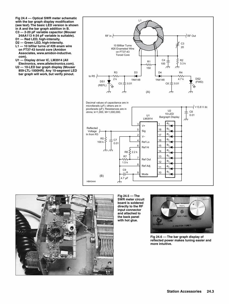
well with high intensity LEDs rather than conventional meters. The SWR meter is built on a small piece of perf-board and mounted to the solder lug on the tuner’s input SO-239. A little hot glue between the perf-board and the back of the chassis adds stability (Fig 24.5).
This broadband circuit works well at the 100-W power level through at least 30 MHz. With careful lead control, it should work up through 6 meters. The transformer is an FT37-43 ferrite core wound with 10 bifilar turns of #26 enameled wire. The primary is just the single wire passing through the center of the toroid. To calibrate the SWR bridge, connect the output to a resistive 50-W load. Apply RF power on any HF band and adjust the 20-pF variable capacitor until the REFL LED goes out.
The FWD LED gives an indication of trans-mitter forward power. You may want to in-crease the value of the 4.7 kW resistor in the FWD circuit if the green LED is too bright. Or you could eliminate this LED and just use the REFL LED.
A BAR-GRAPH DISPLAY FOR THE OPTICAL SWR METER
If you can supply dc power to your Z-Match Tuner and SWR meter, you may want to add the bar graph display as shown in Fig 24.4B to display SWR reflected power. A version of the tuner with bar graph option is shown in Fig 24.6 The nice thing about using the bar graph display is that it seems easier to null the reflected power because the display gives more of an analog meter “feel.” Adjust the Z-Match tuner for minimum brightness of the REFL LED. When this occurs, the SWR should be less than 1.5:1.
This tuner addresses the issues of induc-tor size and finding reasonably priced multi-section variable capacitors. The result is a wide-band, easily adjustable tuner for either portable or base station operation.
HBK0454
Fig 24.2 –– Schematic of the 100-W Z-Match tuner.C1, C2 — 400 pF per section, 2-section
variable capacitor (Oren Elliott S2-399, www.orenelliottproducts.com). If you substitute another variable capacitor, use one with at least 350 pF per section, rated at 500 V RMS minimum.
J1, J2 — SO-239 connectors.S1, S2 — SPDT mini-toggle switch.
T1 — Primary: 22 turns #20 AWG enam wire tapped at 5 and 11 turns. Secondary: 8 turns, with 4 turns either side of the primary 5 turn tap. Wound on T157-6 toroid (Amidon Associates, www.amidon-inductive.com).
Enclosure (Eagle, 40UB103 from www.mouser.com).
Fig 24.3 –– The variable capacitors are insulated from the chassis by mounting them on perforated board. A 1/8-NPT nipple is made into a shaft coupling to couple the insulating shafts to the main capacitor shafts.
OPTICAL HF SWR METER FOR THE Z-MATCH TUNER
While you can use any external SWR meter with the Z-Match tuner — including the SWR meter built into most rigs — the author built an optical SWR meter into the same case for convenience. Refer to Fig 24.4A. It works
Station Accessories 24.3
Fig 24.4 –– Optical SWR meter schematic with the bar graph display modification (see text). The basic LED version is shown in A and the bar graph addition in B.C3 — 2-20 pF variable capacitor (Mouser
24AA113 4-34 pF variable is suitable).D1 — Red LED, high-intensity.D2 — Green LED, high-intensity.L1 — 10 bifilar turns of #26 enam wire
on FT37-43 toroid core (Amidon Associates, www.amidon-inductive.com).
U1 — Display driver IC, LM3914 (All Electronics, www.allelectronics.com).
U2 — 10-LED bar graph display (Mouser 859-LTL-1000HR). Any 10-segment LED bar graph will work, but verify pinout.
Fig 24.5 –– The SWR meter circuit board is soldered directly to the RF input connector and attached to the back panel with hot glue.
Fig 24.6 –– The bar graph display of reflected power makes tuning easier and more intuitive.

24.4 Chapter 24
24.2 A Microprocessor Controlled SWR Monitor
This update of the basic SWR meter, de-signed by Larry Coyle, K1QW, uses a mi-croprocessor to drive an analog panel meter, exploiting the best features of both analog and digital technology. The instrument also displays forward/reflected/net power and return loss (see the Transmission Lines chapter) with peak-hold capability. All dis-play selections are selected by front panel switches. [More information is available on K1QW’s Web site, www.lcbsystems.com, and a complete package of information on this project with supporting files and photos is available on the CD-ROM accompanying this Handbook.]
OVERVIEW AND BLOCk DIAGRAM
After a bit of work, the author came up with the SWR/Power/Return Loss monitor shown in block diagram form in Fig 24.7. There are three interacting assemblies: SWR sense head, front panel assembly and signal processor board. (The latter two make up the Display and Signal Processor unit.) The SWR sense head is a conventional Stockton dual-transformer bridge with Schottky diode detectors. This component converts the for-ward and reflected RF amplitudes to dc and connects to the Display and Signal Processor by an ordinary stereo audio cable.
The user interface to the SWR monitor is familiar and intuitive. As you can see in Fig 24.8A, a front-panel rotary switch selects the quantity to be measured and an analog meter displays the result.Forward power on a linear scaleReflected power as a percentage of for-
ward powerNet power delivered to the load
SWR on a linear scaleReturn loss on a linear scale
Some additional features are:Peak-hold front panel switchA front panel switch to multiply the meter
sensitivity by 3XData logging to a computer using the
USB port.Transmitter Lockout (XLO) at high SWR
The rear panel, Fig 24.8B, shows the power switch and external connections
Transmitter Lockout (XLO) is a protective feature that lights a LED on the front panel and energizes a relay when the SWR exceeds a preset level. This opens a set of relay contacts which are connected to a pair of banana jacks on the rear panel. Once triggered, the relay remains energized for either three or nine seconds, depending on the configuration of the DIP switch located on the signal processor board. The same DIP switch also allows you to
select the SWR level at which the XLO relay triggers — 1.5, 2, 3 or 4:1. By connecting the relay contacts in series with your rig’s PTT or keying line, transmitting into high SWR can be prevented.
The two dc signals from the sense head make up the analog input to the signal pro-cessor board. The analog output for driving the meter is a pulse width modulated (PWM) signal generated by the microprocessor and smoothed by a simple resistor-capacitor (RC) filter.
THE MICROPROCESSORThe Parallax “Propeller” microprocessor
(www.parallax.com) is unique in that it’s re-ally eight processors (“cogs”) in one package, each one able to run its own separate program during its own time slot, controlled by a cen-tral “hub.” This may sound challenging, but this actually makes programming the chip
Fig 24.7 — This block diagram shows how the SWR sense head and the signal processor box are connected by an ordinary two-conductor shielded stereo audio cable. The signal processor box contains the processor board and the front panel assembly.
Fig 24.8 — (A) Front panel of the display and signal processor unit. The meter face and the front panel lettering were created using Microsoft Visio, printed on heavy paper stock and attached with contact cement. With the front cover moved aside, you can see the ribbon cable carrying signals between the front panel assembly and the processor board. (B) Rear panel of the display and signal processor. The mini-B USB connector is accessible through the opening on the top surface of the enclosure.
(A)
(B)
Station Accessories 24.5
much easier. If you need to carry out several tasks at once — and most microprocessor ap-plications do — just assign each job to its own individual cog and work on them separately. The central hub makes sure each cog gets its turn and keeps things synchronized.
The project uses the 3 × 4 inch Propeller USB Development Board from Parallax. It includes the Propeller chip, an Electrically-Erasable Programmable Read-Only Memory (EEPROM) for program storage, a 5 MHz crystal, two voltage regulators and, a USB mini-B connector with all the necessary USB interface circuitry.
The Propeller is programmed in a language called “Spin” which should make anyone who is familiar with the BASIC computer lan-guage feel at home. All the tools you need to write software for and to program the Propel-ler is available for free on the Parallax Web site, including an extensive library of pre-built code routines that you can just drop into your own programs.
Software is loaded onto the development board using the USB port from a host com-puter with a USB port. When not in use as a programming port, the same USB port is used as a serial data port for passing data between the SWR monitor and a computer running a terminal program such as HyperTerminal.
MICROPROCESSOR BOARD CIRCUITRY
The development board includes a proto-typing area large enough to hold all the parts of the SWR monitor except for front and rear panel components. Since most of the parts come assembled on the development board, construction of the digital board is quite easy. As you can see in Fig 24.9A, the electrical schematic, only two integrated circuits and a few analog components are required.
The dc signals representing forward and reflected power from the SWR sense head are received by dual op-amp U2. Each section of U2 is configured as a unity-gain voltage follower with a compensating diode (D1 and D2) to balance out the dc offset introduced by the Schottky rectifier diodes in the sensing head. (The technique of using a diode in the feedback path of an op amp to compensate for the non-linearity of an RF detector diode is de-scribed in detail in “A Compensated, Modular RF Voltmeter” in the Test Equipment and Measurements chapter of this book.) Each section also has an RC low-pass filter at its input to filter out unwanted RF — always a possibility around a ham shack.
The next stage in the signal path is U3, an analog multiplexer (MUX). This chip acts as a three-position switch under control of the microprocessor. (A fourth channel is unused.) The forward and reflected signals (on pins 14 and 15) are sampled alternately, 20 times per second, as long as the program is running. The
Table 24.1BDigital Signals for SWR Threshold SelectXLTHRESH1 XLTHRESH0 SelectsSWR threshold levelOFF OFF 1.5:1OFF ON 2:1ON OFF 3:1ON ON 4:1
Table 24.1ADigital InputsDigitalInput Originatesat WhatitdoesX3SEL front panel - toggle switch increases meter sensitivity by 3XPEAKENBL front panel - toggle switch enables peak hold function on the meterRLOSSEL front panel – rotary switch displays return loss on the meterSWRSEL front panel – rotary switch displays SWR on meterNETSEL front panel – rotary switch displays net power on meterREFSEL front panel – rotary switch displays percent reflected power on meterFWDSEL front panel – rotary switch displays forward power on meterHIREFSEL proc board - DIP switch drives meter to full scale for calibration (must be OFF for normal operation)FASTCAL proc board - DIP switch speeds up meter response for calibration (must be OFF for normal operation)XLOLONG proc board - DIP switch enables long xmtr lockout (about 9 seconds)XLTHRESH0 proc board - DIP switch XLO threshold bit 0XLTHRESH1 proc board - DIP switch XLO threshold bit 1XLOCKENBL rear panel switch enables xmtr lockout functionDIAG proc board - jumper JP1 displays raw input levels on terminalW100 proc board - jumper JP2 changes terminal display to 0-100 watt range (required when using 100-watt sense head)
third input to the MUX (pin 12) is grounded, and is also sampled by the microprocessor from time to time. This gives a measure of any dc offsets introduced by the analog-to-digital conversion and is used to correct the forward and reflected readings in software. This automatic zero adjustment takes place every five seconds or so and is indicated by a brief flash from the front-panel “Calibrating” LED that also serves as a “digital heartbeat” to show that the software is running.
The MUX output (pin 13) is passed to a po-tentiometer voltage divider to allow the scale factor to be set during calibration. From there it goes to the Propeller microprocessor itself where a delta-sigma analog-to-digital con-version takes place. (See the Analog Basics chapter for information on analog-to-digital conversion.)
DIGITAL INPUT/OUTPUTThe microprocessor responds to the user’s
inputs by monitoring the state of 13 digital input pins. Most of these pins are controlled by the rotary and toggle switches on the front panel. The panel connects to the proces- sor board by a short ribbon cable as shown in Fig 24.8A. See Fig 24.9B for a schematic of the separate front panel assembly. The ribbon cable also carries power for the LEDs. On the
processor board there are a multi-section dual in-line package (DIP) switch, S2, and two jumpers, JP1 and JP2, which select among the various operating modes. Lastly, the Xmtr Lockout (XLO) switch is mounted on the rear panel and visible in Fig 24.8B. These inputs to the microprocessor and the various modes of operation they control are summarized in Table 24.1A. The digital inputs are all active low; ie, the function is enabled when the sig-nal line is at a low logic level. XLTHRESH1 and XLTHRESH0 form a two-bit code to select one of four SWR levels. When this SWR level is exceeded and if XLO is enabled, the transmitter lockout function is triggered.
There are only six digital outputs:Two address lines for the analog MUX to
select among the three input channelsTwo lines to power the Calibrating and
XLO LEDs located on the front panelOne PWM signal to drive the front-panel
analog meterOne line to control the XLO relay.Fig 24.8A shows the built-up processor
board inside the 2 × 4 × 6 inch aluminum enclosure connected to the front panel with the ribbon cable. Here you can also see some of the wiring to the rear panel components. The USB connector is at the top edge of the circuit board and is accessible through a rect-angular hole nibbled out of the top surface of the aluminum box.
THE RF SENSE HEADThe SWR sense head is the business end
of the SWR meter where the forward and reflected amplitude components of the RF present on the transmission line are separated and converted to dc. For this project I ad-opted a straightforward Stockton directional coupler circuit, with Schottky diode detec-tors and, unlike other designs, it requires no

24.6 Chapter 24

Station Accessories 24.7
Fig 24.9 — (A) Processor board schematic. All of the parts shown here, except for the rear panel components, are mounted on the Parallax Propeller Development Board. The parts within the dotted line are already installed at the factory, and are shown here only for completeness. (B) Front panel schematic. Switches and LEDs connect to the processor board via a 20-pin dual-row header, J1, and a ribbon cable. For convenience in wiring, the analog meter connects to the processor board by a separate 2-pin connector. (See Parts List on page 24.8.)

24.8 Chapter 24
Fig 24.10 — SWR sense head schematic. All components except for the transformers are surface mount parts. R1 and R2 are size 1210, rated at 1⁄2 W. Transformers T1 and T2 are wound on FT50-43 ferrite toroid cores. For the 10-W sense head, use 10 turns of 24 AWG wire. For the 100-W head, use 31 turns.
Fig 24.11 — (A) SWR plotted against frequency, up to 50 MHz. (B) SWR as a function of input power level at a fixed frequency of 7.2 MHz. The data shown here were taken using the 10-W sense head, with dummy loads measured at 50 and 96.7 W.
balancing trimmers. The schematic is given in Fig 24.10 and the circuit is described in the article by J. Grebenkemper, KA3BLO, “The Tandem Match — an Accurate Directional Wattmeter,” QST, Jan 1987, pp 18-26 (also published in the 2009 and earlier editions of The ARRL Handbook).
The accuracy of this circuit can be greatly improved by taking care to match the diodes in the sensing head with the corresponding compensation diodes in the op amp input stages on the signal processor board (D1 and D2 in Fig 24.9A). The easiest way to do this is with the diode test function included on most utility digital multimeters which passes a small dc cur-rent through the diode being tested and displays the forward voltage drop. The high-frequency range can be extended by using surface-mount components in the sensing head.
There are two versions of the SWR sensing head. The QRP version has a maximum range of 10 W. The other can handle up to 100 W. The only difference between the two versions is the number of turns on the toroid transform-ers (see the parts list in Fig 24.10). The high frequency performance of the 100-W head at 50 MHz proved to be poorer than the 10-W unit. I attribute this to the added capacitance
of the transformer windings (the higher power transformers have three times as many turns as the low-power ones).
The overall accuracy of the monitor compares fairly well to commercial devices. Fig 24.11A and 24.11B show performance data I took using dummy loads of 50 and 96.7 W. At five watts input, using the 10-W sensing head, the SWR readings were with- in 3% over a range of 1.8 to 30 MHz, and within 5% at 50 MHz. Fig 24.11B shows good accuracy down to 500 mW input (great for QRP rigs!) and is even usable down to 250 mW.
24.4.6 SoftwareFor those who want to duplicate this proj-
ect, the Spin language software listing, ready to program into the Parallax USB Develop-ment Board, is available in the package of
Parts List for Figure 29 on previous 2 pages.Parts List – Processor BoardC3, C7 — 0.22 µF ceramic capacitorC1, C2 — 0.1 µF ceramic capacitorC4, C6 — 0.01 µF ceramic capacitorC8-C11 — 10 µF, 16 V electrolytic
capacitorD1, D2 — 1N5711 Schottky diodeD3, D4 — 1N5818 Schottky diodeJ6 — 20-pin dual row headerJP1, JP2 — single jumper headerk1 — SPDT 5 V relayQ1 — 2N4401 NPN transistorR3, R8, R9, R14, R22, R24, R26 — 1.5 kW,
1⁄8 W, 5% resistorR4, R5, R10, R12, R13, R17, R18, R19, R20,
R21, R23, R27, R28 — 100 kW, 1⁄8 W, 5% resistor
R6 — 10 kW trim pot, 25 turnsR7 — 82 kW, 1⁄8 W, 5% resistorR11 — 4.7 kW, 1⁄8 W, 5% resistorR15 — 1 kW, 1⁄8 W, 5% resistorR16 — 1.0 kW trim pot, 25 turnsS2 — 7-position DIP switchU2 — TLV2462CP dual op ampU3 — 74HC4052N dual 4-channel MUXParallax Proto USB Development Board,
Part # 32812Parts List – Front PanelDS1 — yellow LEDDS2 — red LEDDS3 — green LEDJ1 — 20-pin dual row headerR1, R2, R7, R8, R9, R10, R11 — 100 kW,
1⁄8 W, 5% resistorR4, R5, R6 — 1.5 kW, 1⁄8 W, 5% resistorR3, R12, R13 — 330 W, 1⁄8 W, 5% resistorS1, S2 — SPST toggle switchS3 — 5-position rotary switch0-1 mA dc meter
Station Accessories 24.9
supporting files on the CD-ROM. There are also details of the subroutines handled by each of the Propeller cogs plus additional text and graphic files covering operation and features of the instrument.
As explained above, the organization of the Propeller into several peripheral processors (cogs) makes it easy to follow the program flow. The main program object (MAIN) runs in its own cog and is the first to be executed when power is applied (or whenever the chip is reset). Its first order of business is to set individual microprocessor pins to be inputs or outputs, as required.
Next, MAIN starts up three separate cogs
for (1) analog-to-digital conversion (the ADC3CH cog), (2) generating the pulse width modulated waveform to drive the analog panel meter (the PWM cog) and (3) communicat-ing with the terminal via the USB port (the MONITOR cog). They run continuously, swapping data with the MAIN program by means of variables stored in memory. After these three cogs are started, the MAIN pro-gram object enters a loop, endlessly repeating the following steps:
1) Read forward and reflected amplitudes and SWR data generated by the ADC3CH object.
2) Calculate forward power, percent re-
flected power, net power, SWR and return loss in decibels.
3) Display the quantity selected by the front panel switch on the panel meter using the PWM object.
4) Convert power levels, SWR and return loss information to ASCII strings and send them to the MONITOR object, which writes to the USB port.
This is a shining example of building on the accomplishments of others who have made their work freely available. Without such an extensive library of pre-tested routines on hand, the author probably would never have even started this project.
Table 24.2Parts List: 160/80-Meter Impedance Matching Assembly
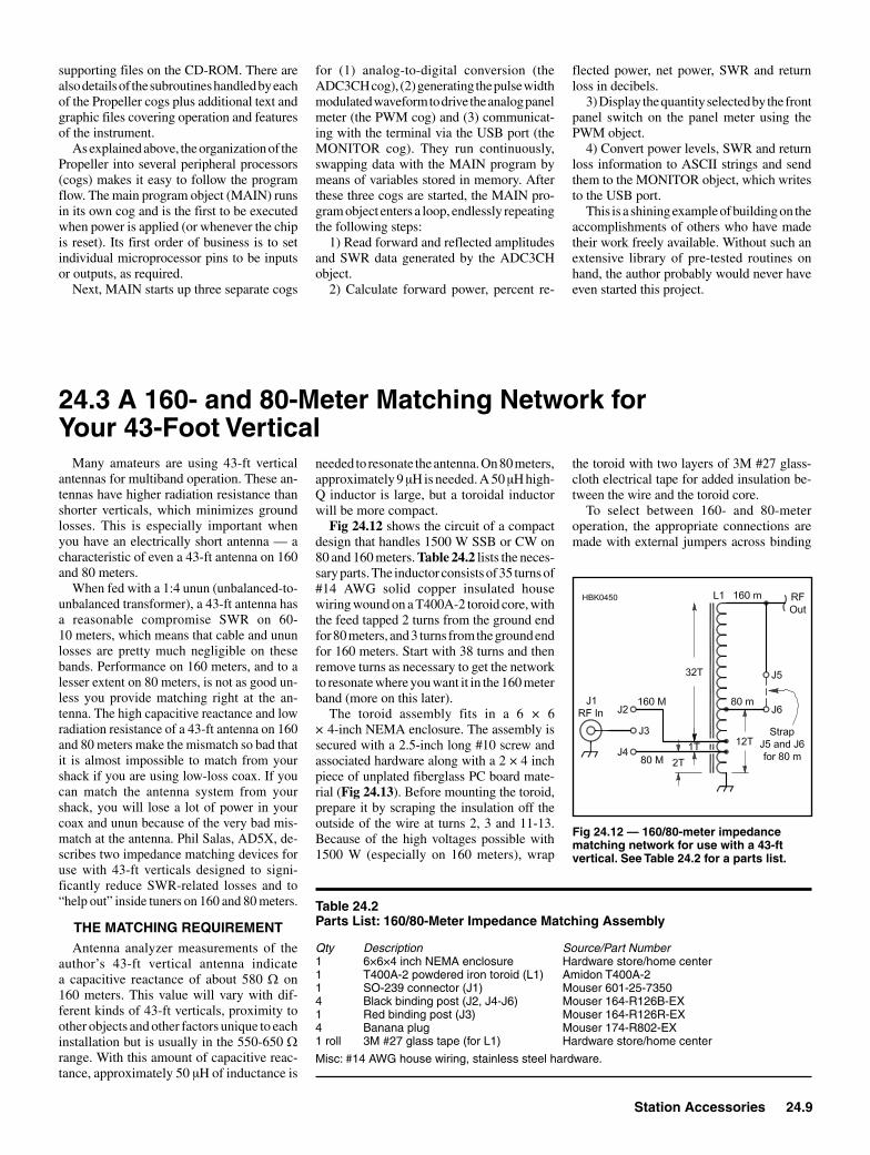
Qty Description Source/PartNumber1 6×6×4 inch NEMA enclosure Hardware store/home center1 T400A-2 powdered iron toroid (L1) Amidon T400A-21 SO-239 connector (J1) Mouser 601-25-73504 Black binding post (J2, J4-J6) Mouser 164-R126B-EX1 Red binding post (J3) Mouser 164-R126R-EX4 Banana plug Mouser 174-R802-EX1 roll 3M #27 glass tape (for L1) Hardware store/home center
Misc: #14 AWG house wiring, stainless steel hardware.
Fig 24.12 — 160/80-meter impedance matching network for use with a 43-ft vertical. See Table 24.2 for a parts list.
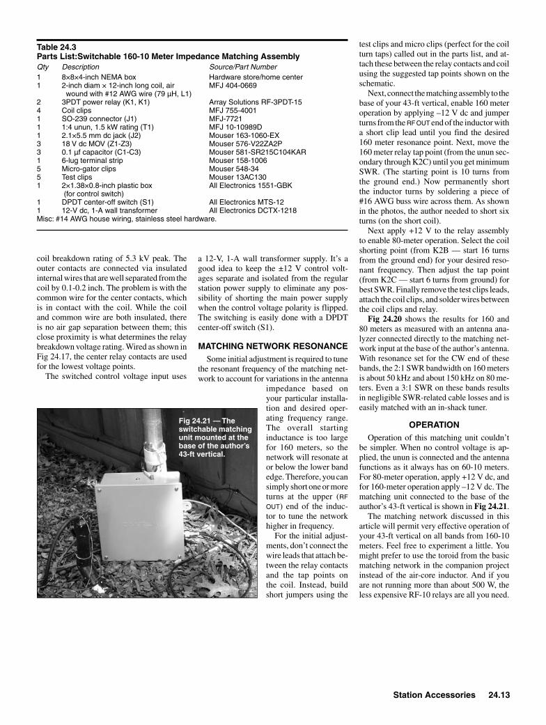
24.3 A 160- and 80-Meter Matching Network for Your 43-Foot Vertical
Many amateurs are using 43-ft vertical antennas for multiband operation. These an-tennas have higher radiation resistance than shorter verticals, which minimizes ground losses. This is especially important when you have an electrically short antenna — a characteristic of even a 43-ft antenna on 160 and 80 meters.
When fed with a 1:4 unun (unbalanced-to-unbalanced transformer), a 43-ft antenna has a reasonable compromise SWR on 60- 10 meters, which means that cable and unun losses are pretty much negligible on these bands. Performance on 160 meters, and to a lesser extent on 80 meters, is not as good un-less you provide matching right at the an-tenna. The high capacitive reactance and low radiation resistance of a 43-ft antenna on 160 and 80 meters make the mismatch so bad that it is almost impossible to match from your shack if you are using low-loss coax. If you can match the antenna system from your shack, you will lose a lot of power in your coax and unun because of the very bad mis-match at the antenna. Phil Salas, AD5X, de-scribes two im pedance matching devices for use with 43-ft verticals designed to signi-ficantly reduce SWR-related losses and to “help out” inside tuners on 160 and 80 meters.
THE MATCHING REQUIREMENTAntenna analyzer measurements of the
author’s 43-ft vertical antenna indicate a capacitive reactance of about 580 W on 160 meters. This value will vary with dif-ferent kinds of 43-ft verticals, proximity to other objects and other factors unique to each installation but is usually in the 550-650 W range. With this amount of capacitive reac-tance, approximately 50 µH of inductance is
needed to resonate the antenna. On 80 meters, approximately 9 µH is needed. A 50 µH high-Q inductor is large, but a toroidal inductor will be more compact.
Fig 24.12 shows the circuit of a compact design that handles 1500 W SSB or CW on 80 and 160 meters. Table 24.2 lists the neces-sary parts. The inductor consists of 35 turns of #14 AWG solid copper insulated house wiring wound on a T400A-2 toroid core, with the feed tapped 2 turns from the ground end for 80 meters, and 3 turns from the ground end for 160 meters. Start with 38 turns and then remove turns as necessary to get the network to resonate where you want it in the 160 meter band (more on this later).
The toroid assembly fits in a 6 × 6 × 4-inch NEMA enclosure. The assembly is secured with a 2.5-inch long #10 screw and associated hardware along with a 2 × 4 inch piece of unplated fiberglass PC board mate-rial (Fig 24.13). Before mounting the toroid, prepare it by scraping the insulation off the outside of the wire at turns 2, 3 and 11-13. Because of the high voltages possible with 1500 W (especially on 160 meters), wrap
the toroid with two layers of 3M #27 glass-cloth electrical tape for added insulation be-tween the wire and the toroid core.
To select between 160- and 80-meter operation, the appropriate connections are made with external jumpers across binding
24.10 Chapter 24
posts as shown in Fig 24.14. Stainless steel #8 hardware (screws, washers, lockwashers, nuts) is used for the matching unit ground and RF output. Internal to the matching unit, a 2-inch-wide strip of aluminum duct repair tape makes a good low-impedance ground between the coax connector and the ground screw on the bottom of the case. Finally, use #14 AWG stranded insulated wire for all in-ternal connections.
TUNING THE MATCHING NETWORk TO RESONANCE
Your particular installation will almost certainly require you to change the resonant frequency of the matching network. This is because there will be variations of the antenna impedance based on your particular installa-tion and desired operating frequency range. The design is such that the overall inductance is too large for 160 meters, so the network should resonate at or below the lower band edge. Therefore, you will need to remove one or more of the upper inductor turns to reso-nate the network for the desired frequency on 160 meters. To do this, first solder wires from the turn 2 and 3 tap points on the coil to the two outer binding posts by the RF IN con-nector. The input tap points tend to be fairly non-critical and will probably always be the same for all installations.
Now solder a short wire from the RF IN center pin to the middle binding post. Next, externally jumper the middle binding post to the 160 meter binding post (turn 3). Connect the matching assembly to the base of your
these bands results in negligible SWR-related cable losses and is easily matched with an in-shack tuner.
OPERATIONUsing the matching unit is simple. Just
disconnect your normal unun when you want to operate on 160 or 80 meters and connect this matching unit to the base of the antenna. Select either 160 or 80 meters with the ex-ternal straps. You can connect both the unun and this matching unit to the antenna at the same time, and just leave off the ground wire from the unit that is not used. The matching unit connected to the base of a 43-ft vertical is shown in Fig 24.16.
Fig 24.13 — Mounting details of the toroidal inductor for the 160/80-meters matching unit. The input side of the enclosure is on the left. Coax to the station connects to the RF IN SO-239, and a strap between the center binding post and one of the outer posts selects the input tap for operation on 160 or 80 meters. On the right side, a jumper between the two binding posts shorts a section of the coil for 80-meter operation. The RF OUT connection to the base of the antenna is made with via the #8 machine screw and hardware at the top, and the ground connection is on the bottom.
(A)
(B)Fig 24.14 — Binding posts are used for jumpers to select 160 or 80 meter operation.
43-ft vertical and use an antenna analyzer to find the minimum SWR point on 160 meters. If the resonant frequency is too low, remove a turn of wire and measure againch You should see a 50 kHz upward move in frequency per turn of wire removed.
When you have reached the desired reso-nant point on 160 meters, it is time to move to 80 meters. Externally jumper the input tap middle binding post to the 80-meter binding post (turn 2), and use a clip lead to short from the top of the coil to about turn 12. Again, find the frequency where minimum SWR occurs. Move the tap point up or down until you reach the desired resonance point. Solder a wire from this tap point to one of the binding posts. Solder another wire from the top of the coil to another binding post. Now you will be able to externally jumper these binding posts to go from 160 to 80 meters.
Fig 24.15 shows the author’s final results for 160 and 80 meters as measured with an antenna analyzer connected directly to the matching network input at the base of the antenna. With resonance set for the CW end of these bands, the 2:1 SWR bandwidth on 160 meters is about 50 kHz and about 150 kHz on 80 meters. Even a 3:1 SWR on
Fig 24.15 — Measured at the antenna base, the 2:1 SWR bandwidth is about 50 kHz for 160 meters and 150 kHz for 80 meters.
Fig 24.16 — The finished matching unit at the base of the author’s 43-ft antenna (strapped for 80 meter operation).
Station Accessories 24.11
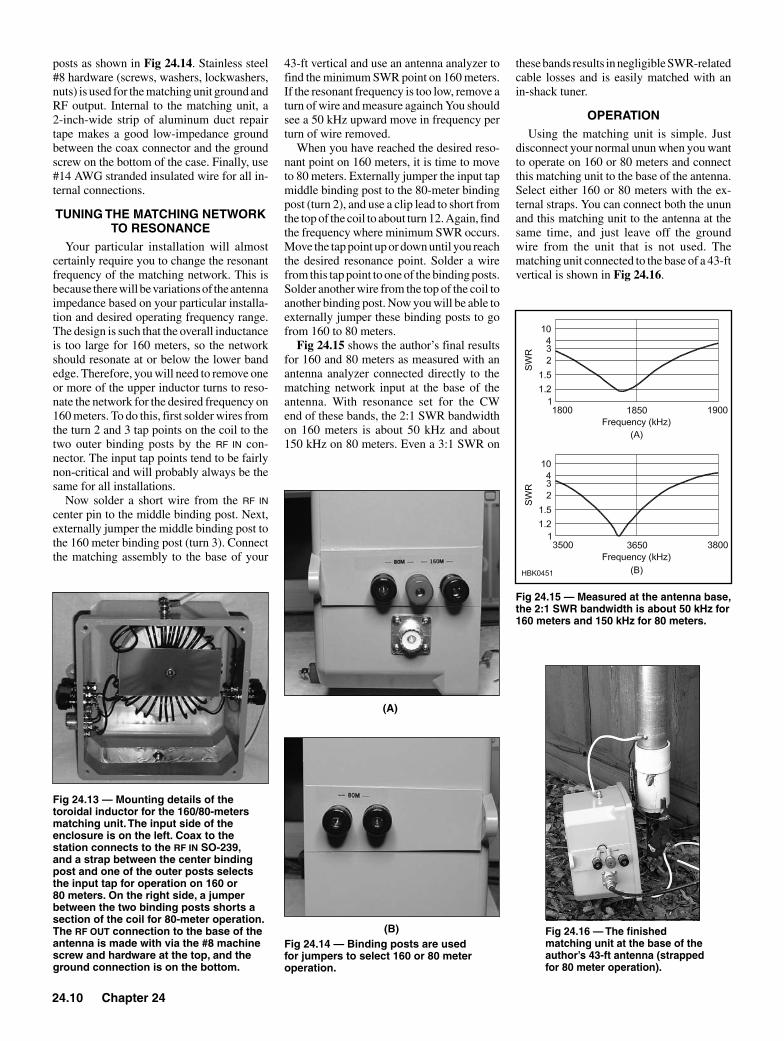
24.4 Switching the Matching Network for Your 43-Foot Vertical
Another project in this chapter describes a simple 160 and 80 meter impedance match-ing network for installation at the base of a 43-ft vertical antenna. While that unit is very effective and inexpensive to build, it is also a little inconvenient in that you must connect it when it is needed, and you must also manu-ally enable 160 or 80 meter operation using jumpers. Phil Salas, AD5X, enhances the original design with a more versatile match-ing assembly that can be controlled remotely for operation on all bands.
FIRST — A WORD ABOUT RF VOLTAGES
This unit uses relays for selecting the dif-ferent bands, so a discussion of RF voltages is appropriate. RF voltages at the base of an untuned vertical can be quite high. As the antenna becomes shorter, the capacitive re-actance becomes higher and so the resultant voltage drop across the combination of reac-tance and radiation resistance increases. With the 43-ft vertical, the worst-case situation will occur on 160 meters where the capacitive re-actance is approximately 600 W. The radiation resistance is approximately 3 W.
With a perfect ground (no ground loss) and 1500 W of power properly matched to the antenna, peak RF voltage works out to about 19,000 Vpk:
= W =
= + = W
= × =
= × =
2 2
RMS
pk
I 1500 W / 3 22.4 A
Z 3 600 600
V 22.4 600 13,440 V
V 13,440 1.414 19,004 V
Very few hams have a ground system that is lossless. With a ground loss of 10 W (better than most hams have), it works out to about 9100 Vpk. With the author’s 600-W amplifier, assuming a ground loss of 10 W, it’s about 5800 Vpk.
The author experimented with two dif-ferent relays from Array Solutions. The RF-10 DPDT relay has 1.7 kVpk contact-to-contact and 3.1 kVpk contact-to-coil voltage breakdown ratings. This relay proved to be a good solution for up to about 500 W on 160 meters when the two sets of contacts are put in series. The second relay is the RF-3PDT-15 which has 3.1 kVpk contact-to-contact and 5.3 kVpk contact-to-coil volt-age breakdown ratings. This relay has nearly twice the contact breakdown rating of the RF-10, and it’s 3PDT so an additional set of contacts can be put in series to increase the breakdown voltage. This relay can be used in a full legal limit application if applied properly in the circuit (more on this later).
Depending on your power level and ground losses, the less expensive and smaller RF-10 may be all you need. Make the calculations to determine which relay is more appropriate for you. If you look for alternative relays, pay attention to the breakdown voltage rating; it’s hard to find relays with suitable ratings for this application. The Array Solutions relays have 30 A contacts, but 15 A or more should be sufficient.
THE ALL-BAND MATCHING SOLUTION
As explained in the companion project de-scribing a simple matching network, when fed with a 1:4 unun (unbalanced-to-unbalanced transformer), a 43-ft antenna has a reason-able compromise SWR on 60-10 meters. The antenna requires approximately 50 µH of inductance to resonate on 160 meters and
9 µH on 80 meters. For convenient all-band operation from the shack, the solution shown in Fig 24.17 uses two relays to switch in the unun for 60-10 meter operation or the appro-priate inductance for 160 and 80 meters. The unit will handle up to 1500 W from 160- 10 meters.
Relay control requires inputs of 0 V, +12 V dc or –12 V dc. The matching unit operates as follows:
• With no control voltage applied, the 1:4 unun is connected to the antenna for 60- 10 meter operation, and the inductor is dis-connected, so the original antenna compro-mise SWR on these bands is preserved.
• With +12 V applied for 80-meter opera-tion, K1 and K2 close. Contact K1C connects the unun secondary to L1 through K2C at the 200 W point (6 turns from the ground end). Contacts K2A and K2B short out the top part
Fig 24.17 — This switched impedance matching network for use with a 43-ft vertical allows operation on 160-10 meters and is controlled from the station operating position. See Table 24.3 for a parts list.
24.12 Chapter 24
of L1 (about 16 turns from the ground end), resonating the antenna on 80 meters.
• When the voltage is reversed (–12 V) for 160-meter operation, K1 stays closed but K2 opens. K2C now connects the unun secondary to L1 at the 200 W point for 160 meters (10 turns from the ground end). Contacts K2A and K2B open, removing the short and allowing the entire coil to be used to resonate the antenna on 160 meters.
Connecting the unun to L1 at the 200 W point keeps the unun secondary voltage rea-sonable, and the feed line and unun losses very low as well.
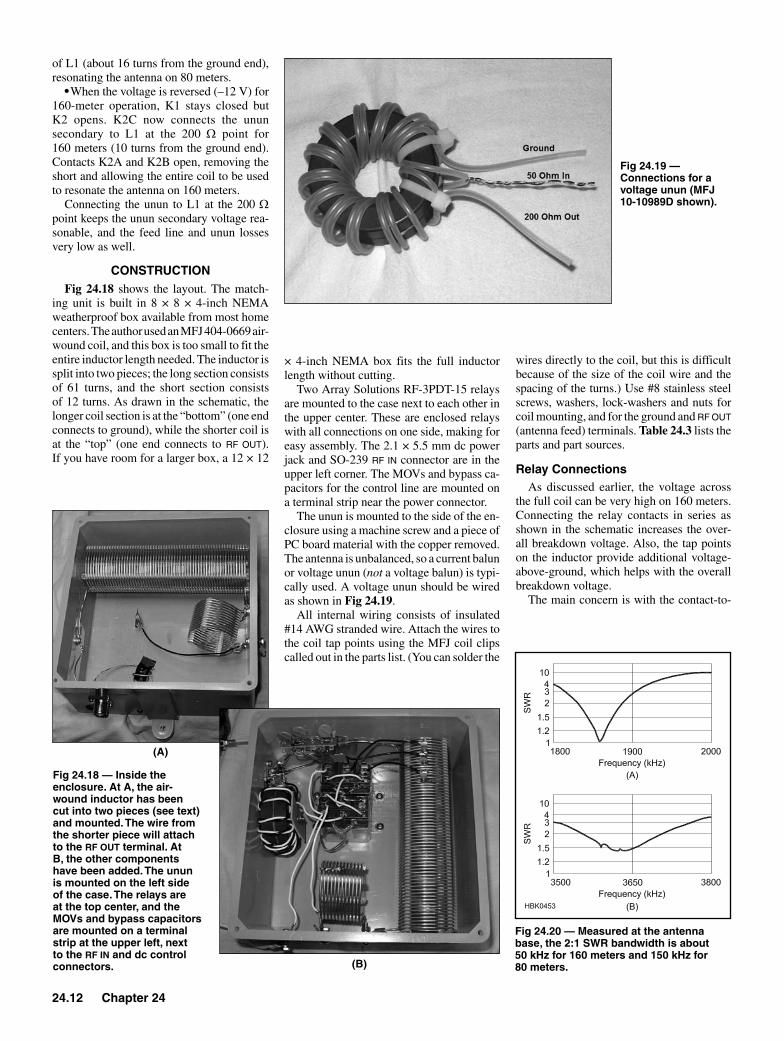
CONSTRUCTIONFig 24.18 shows the layout. The match-
ing unit is built in 8 × 8 × 4-inch NEMA weatherproof box available from most home centers. The author used an MFJ 404-0669 air-wound coil, and this box is too small to fit the entire inductor length needed. The inductor is split into two pieces; the long section consists of 61 turns, and the short section consists of 12 turns. As drawn in the schematic, the longer coil section is at the “bottom” (one end connects to ground), while the shorter coil is at the “top” (one end connects to RF OUT). If you have room for a larger box, a 12 × 12
Fig 24.18 — Inside the enclosure. At A, the air-wound inductor has been cut into two pieces (see text) and mounted. The wire from the shorter piece will attach to the RF OUT terminal. At B, the other components have been added. The unun is mounted on the left side of the case. The relays are at the top center, and the MOVs and bypass capacitors are mounted on a terminal strip at the upper left, next to the RF IN and dc control connectors.
(A)
(B)
× 4-inch NEMA box fits the full inductor length without cutting.
Two Array Solutions RF-3PDT-15 relays are mounted to the case next to each other in the upper center. These are enclosed relays with all connections on one side, making for easy assembly. The 2.1 × 5.5 mm dc power jack and SO-239 RF IN connector are in the upper left corner. The MOVs and bypass ca-pacitors for the control line are mounted on a terminal strip near the power connector.
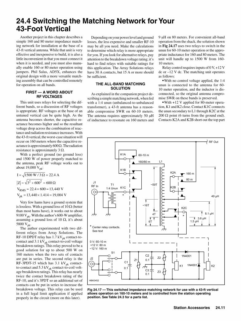
The unun is mounted to the side of the en-closure using a machine screw and a piece of PC board material with the copper removed. The antenna is unbalanced, so a current balun or voltage unun (not a voltage balun) is typi-cally used. A voltage unun should be wired as shown in Fig 24.19.
All internal wiring consists of insulated #14 AWG stranded wire. Attach the wires to the coil tap points using the MFJ coil clips called out in the parts list. (You can solder the
wires directly to the coil, but this is difficult because of the size of the coil wire and the spacing of the turns.) Use #8 stainless steel screws, washers, lock-washers and nuts for coil mounting, and for the ground and RF OUT (antenna feed) terminals. Table 24.3 lists the parts and part sources.
Relay ConnectionsAs discussed earlier, the voltage across
the full coil can be very high on 160 meters. Connecting the relay contacts in series as shown in the schematic increases the over-all breakdown voltage. Also, the tap points on the inductor provide additional voltage-above-ground, which helps with the overall breakdown voltage.
The main concern is with the contact-to-
Fig 24.19 — Connections for a voltage unun (MFJ 10-10989D shown).
Fig 24.20 — Measured at the antenna base, the 2:1 SWR bandwidth is about 50 kHz for 160 meters and 150 kHz for 80 meters.
Station Accessories 24.13
a 12-V, 1-A wall transformer supply. It’s a good idea to keep the ±12 V control volt-ages separate and isolated from the regular station power supply to eliminate any pos-sibility of shorting the main power supply when the control voltage polarity is flipped. The switching is easily done with a DPDT center-off switch (S1).
MATCHING NETWORk RESONANCESome initial adjustment is required to tune
the resonant frequency of the matching net-work to account for variations in the antenna
impedance based on your particular installa-tion and desired oper-ating frequency range. The overall starting inductance is too large for 160 meters, so the network will resonate at or below the lower band edge. Therefore, you can simply short one or more turns at the upper (RF
OUT) end of the induc-tor to tune the network higher in frequency.
For the initial adjust-ments, don’t connect the wire leads that attach be-tween the relay contacts and the tap points on the coil. Instead, build short jumpers using the
test clips and micro clips (perfect for the coil turn taps) called out in the parts list, and at-tach these between the relay contacts and coil using the suggested tap points shown on the schematic.
Next, connect the matching assembly to the base of your 43-ft vertical, enable 160 meter operation by applying –12 V dc and jumper turns from the RF OUT end of the inductor with a short clip lead until you find the desired 160 meter resonance point. Next, move the 160 meter relay tap point (from the unun sec-ondary through K2C) until you get minimum SWR. (The starting point is 10 turns from the ground end.) Now permanently short the inductor turns by soldering a piece of #16 AWG buss wire across them. As shown in the photos, the author needed to short six turns (on the short coil).
Next apply +12 V to the relay assembly to enable 80-meter operation. Select the coil shorting point (from K2B — start 16 turns from the ground end) for your desired reso-nant frequency. Then adjust the tap point (from K2C — start 6 turns from ground) for best SWR. Finally remove the test clips leads, attach the coil clips, and solder wires between the coil clips and relay.
Fig 24.20 shows the results for 160 and 80 meters as measured with an antenna ana-lyzer connected directly to the matching net-work input at the base of the author’s antenna. With resonance set for the CW end of these bands, the 2:1 SWR bandwidth on 160 meters is about 50 kHz and about 150 kHz on 80 me-ters. Even a 3:1 SWR on these bands results in negligible SWR-related cable losses and is easily matched with an in-shack tuner.
OPERATIONOperation of this matching unit couldn’t
be simpler. When no control voltage is ap-plied, the unun is connected and the antenna functions as it always has on 60-10 meters. For 80-meter operation, apply +12 V dc, and for 160-meter operation apply –12 V dc. The matching unit connected to the base of the author’s 43-ft vertical is shown in Fig 24.21.
The matching network discussed in this article will permit very effective operation of your 43-ft vertical on all bands from 160-10 meters. Feel free to experiment a little. You might prefer to use the toroid from the basic matching network in the companion project instead of the air-core inductor. And if you are not running more than about 500 W, the less expensive RF-10 relays are all you need.
Table 24.3Parts List:Switchable 160-10 Meter Impedance Matching AssemblyQty Description Source/PartNumber1 8×8×4-inch NEMA box Hardware store/home center1 2-inch diam × 12-inch long coil, air MFJ 404-0669 wound with #12 AWG wire (79 µH, L1) 2 3PDT power relay (K1, K1) Array Solutions RF-3PDT-154 Coil clips MFJ 755-40011 SO-239 connector (J1) MFJ-77211 1:4 unun, 1.5 kW rating (T1) MFJ 10-10989D1 2.1×5.5 mm dc jack (J2) Mouser 163-1060-EX3 18 V dc MOV (Z1-Z3) Mouser 576-V22ZA2P3 0.1 µf capacitor (C1-C3) Mouser 581-SR215C104KAR1 6-lug terminal strip Mouser 158-10065 Micro-gator clips Mouser 548-345 Test clips Mouser 13AC1301 2×1.38×0.8-inch plastic box All Electronics 1551-GBK (for control switch) 1 DPDT center-off switch (S1) All Electronics MTS-121 12-V dc, 1-A wall transformer All Electronics DCTX-1218Misc: #14 AWG house wiring, stainless steel hardware.
Fig 24.21 — The switchable matching unit mounted at the base of the author’s 43-ft vertical.
coil breakdown rating of 5.3 kV peak. The outer contacts are connected via insulated internal wires that are well separated from the coil by 0.1-0.2 inch. The problem is with the common wire for the center contacts, which is in contact with the coil. While the coil and common wire are both insulated, there is no air gap separation between them; this close proximity is what determines the relay breakdown voltage rating. Wired as shown in Fig 24.17, the center relay contacts are used for the lowest voltage points.
The switched control voltage input uses

24.14 Chapter 24
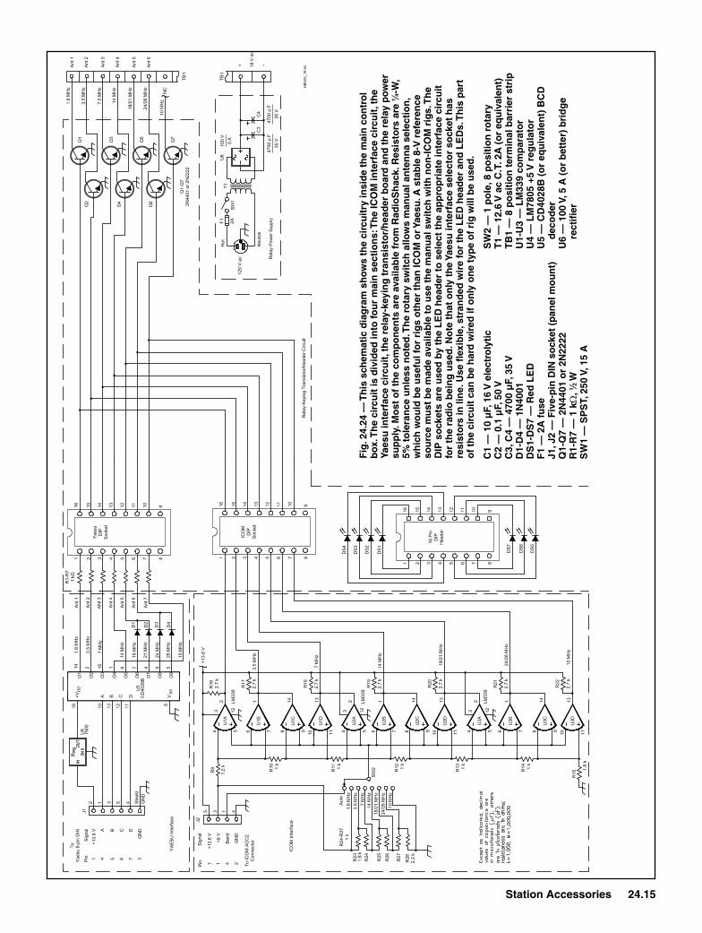
24.5 An External Automatic Antenna Switch for Use With Yaesu or ICOM Radios
This antenna-switching-control project in-volves a combination of ideas from several earlier published articles.1,2,3 This system was designed to mount the antenna relay box outside the shack, such as on a tower. With this arrangement, only a single an-tenna feed line needs to be brought into the shack. Fig 24.22 shows the control unit and relay box, designed and built by Joe Carcia, NJ1Q. Either an ICOM or Yaesu HF radio will automatically select the proper antenna. In addition, a manual switch can override the ICOM automatic selection. That feature also provides a way to use the antenna with other radios. The antenna switch is not a two-radio switch, though. It will only work with one radio at a time.
Many builders may want to use only the ICOM or only the Yaesu portion of the in-terface circuitry, depending on the brand of radio they own. The project is a “hacker’s dream.” It can be built in a variety of forms, with the only limitations being the builder’s imagination.
CIRCUIT DESCRIPTIONFig 24.23 is a block diagram of the com-
plete system. An ICOM or Yaesu HF radio connects to the appropriate decoder via the accessory connector on the back of the radio. Some other modern rigs have an accessory connector used for automatic bandswitching of amplifiers, tuners and other equipment. For example, Ten-Tec radios apply a 10 to 14-V dc signal to pins on the DB-25 interface con-nector for the various bands. Other radios use particular voltages on one of the accessory-connector pins to indicate the selected band. Check the owner’s manual of your radio for specific information, or contact the manufac-turer’s service department for more details. You may be able to adapt the ideas presented in this project for use with other radios.
A single length of coax and a multiconduc-
Fig 24.22 — Automatic antenna switch relay box (left) and control box (right).
Table 24.5Yaesu Band Data Voltage Output (BCD)Band A B C D (BCDEquiv.) (1) (2) (4) (8)1.8 5V 0V 0V 0V 13.5 0V 5V 0V 0V 27.0 5V 5V 0V 0V 310.1 0V 0V 5V 0V 414 5V 0V 5V 0V 518.068 0V 5V 5V 0V 621 5V 5V 5V 0V 724.89 0V 0V 0V 5V 828 5V 0V 0V 5V 9
Fig 24.23 — Block diagram of the remotely controlled automatic antenna switch.
Table 24.4ICOM Accessory Connector OutputVoltages By BandBand(MHz) OutputVoltage1.8 7 – 8.03.5 6 – 6.57 5 – 5.514 4 – 4.518, 21 3 – 3.524, 28 2 – 2.510 0 – 1.2
Note: The voltage step between bands isnot constant, but close to 1.0 V, and the10-MHz band is not in sequence with theothers.
tor control cable run from the rig and decoder/control box to the remotely located switch unit. The remote relay box is equipped with SO-239 connectors for the input as well as the output to each antenna. You can use any type of connectors, though.
ICOM radios use an 8-V reference and a voltage divider system to provide a stepped band-data output voltage. Table 24.4 shows the output voltage at the accessory socket
when the radio is switched to the various bands. Notice that seven voltage steps can be used to select different antennas. The ICOM accessory connector pin assignments needed for this project are:
Pin 1 +8 V referencePin 2 GroundPin 4 Band signal voltagePin 7 +12 (13.8) V supplyYaesu radios provide the band information
Station Accessories 24.15
Fig
. 24.
24 —
Th
is s
chem
atic
dia
gra
m s
ho
ws
the
circ
uit
ry in
sid
e th
e m
ain
co
ntr
ol
box
. Th
e ci
rcu
it is
div
ided
into
fou
r m
ain
sec
tio
ns:
Th
e IC
OM
inte
rfac
e ci
rcu
it, t
he
Yaes
u in
terf
ace
circ
uit
, th
e re
lay-
keyi
ng
tra
nsi
sto
r/h
ead
er b
oar
d a
nd
th
e re
lay
po
wer
su
pp
ly. M
ost
of
the
com
po
nen
ts a
re a
vaila
ble
fro
m R
adio
Sh
ack.
Res
isto
rs a
re 1 ⁄4
-W,
5% t
ole
ran
ce u
nle
ss n
ote
d. T
he
rota
ry s
wit
ch a
llow
s m
anu
al a
nte
nn
a se
lect
ion
, w
hic
h w
ou
ld b
e u
sefu
l fo
r ri
gs
oth
er t
han
ICO
M o
r Yae
su. A
sta
ble
8-V
ref
eren
ce
sou
rce
mu
st b
e m
ade
avai
lab
le t
o u
se t
he
man
ual
sw
itch
wit
h n
on
-IC
OM
rig
s. T
he
DIP
so
cket
s ar
e u
sed
by
the
LE
D h
ead
er t
o s
elec
t th
e ap
pro
pri
ate
inte
rfac
e ci
rcu
it
for
the
rad
io b
ein
g u
sed
. No
te t
hat
on
ly t
he
Yaes
u in
terf
ace
sele
cto
r so
cket
has
re
sist
ors
in li
ne.
Use
flex
ible
, str
and
ed w
ire
for
the
LE
D h
ead
er a
nd
LE
Ds.
Th
is p
art
of
the
circ
uit
can
be
har
d w
ired
if o
nly
on
e ty
pe
of
rig
will
be
use
d.
C1
— 1
0 µ
F, 1
6 V
ele
ctro
lyti
cC
2 —
0.1
µF,
50
VC
3, C
4 —
470
0 µ
F, 3
5 V
D1-
D4
— 1
N40
01D
S1-
DS
7 —
Red
LE
DF
1 —
2A
fu
seJ1
, J2
— F
ive-
pin
DIN
so
cket
(p
anel
mo
un
t)Q
1-Q
7 —
2N
4401
or
2N22
22R
1-R
7 —
1 k
W, 1 ⁄2
WS
W1
— S
PS
T, 2
50 V
, 15
A
SW
2 —
1 p
ole
, 8 p
osi
tio
n r
ota
ryT
1 —
12.
6 V
ac
C.T
. 2A
(o
r eq
uiv
alen
t)T
B1
— 8
po
siti
on
ter
min
al b
arri
er s
trip
U1-
U3
— L
M33
9 co
mp
arat
or
U4
— L
M78
05 +
5 V
reg
ula
tor
U5
— C
D40
28B
(o
r eq
uiv
alen
t) B
CD
d
eco
der
U6
— 1
00 V
, 5 A
(o
r b
ette
r) b
rid
ge
rect
ifier

24.16 Chapter 24
as binary coded decimal (BCD) data on four lines. Nine different BCD values allow you to select a different antenna for each of the MF/HF bands. Table 24.5 shows the BCD data from Yaesu radios for the various bands. The Yaesu 8-pin DIN accessory connector pin assignments needed for this project are:
Pin 1 +12 (13.8) V supplyPin 3 GroundPin 4 Band Data APin 5 Band Data BPin 6 Band Data CPin 7 Band Data D
Fig 24.24 is the schematic diagram for the control box. We will discuss each part of the control circuit later in this description. First, let’s turn our attention to the external antenna box.
EXTERNAL ANTENNA BOXOnly the number of control lines going
out to the relay box limits the number of antennas this relay box will switch. The unit shown in the photos has 10 SO-239 connec-tors, to switch the common feed line to any of nine antennas. Many hams will use an eight-conductor rotator cable (such as Belden 9405) to the relay box. Using eight wires, we can control seven relays (six for antennas and one to ground the feed line for lightning protection) plus the relay coil power supply and ground lead. The photos show eight re-lays, and the box can be expanded further if desired. There is also a connector for power and control lines. Use of a DB-15 allows for the addition of more relays and control lines later. A DB-9 connector would be suitable for use with the eight-conductor control cable, or you may wish to use a weatherproof connec-tor. Fig 24.25 shows the relay box schematic diagram.
Since the box will be located outside, use a weatherproof metal box — a Ham-mond Manufacturing, type 1590Z150, watertight aluminum box is shown. It’s about 8.5×4.25×3.125 inches. This is a rather hefty box, meant to be exposed to years of various weather conditions. You can, however, use almost anything.
The coax connectors are mounted so each particular antenna connector is close to the relay, without too much crowding. For added weather protection (and conductivity), apply Penetrox to the connector flange mount, in-cluding the threads of the mounting screws. On the power/control line connector, use Coax Seal or other flexible cable sealant.
The aluminum angle stock on either side of the box is for mounting to a tower leg. The U-bolts should be of the proper size to fit the tower leg. They should also be galvanized or made of stainless steel.
ANTENNA RELAYSOne of the more difficult parts of this proj-
ect was the modification of the relays (DPDT Omron LY2F-DC12). To improve isolation, the moveable contacts (armature) are wired in parallel and the connecting wire is routed through a hole in the relay case.
Remove the relay from its plastic case. Un-solder and remove the small wires from the armatures. Carefully solder a jumper across
the armature lugs with #20 solid copper. Then solder a piece of very flexible wire (such as braid from RG-58 cable) to either armature lug. Obviously, the location of the wire de-pends on which side you wish to connect the SO-239. You will also need to make a hole in the plastic case that is large enough to accommodate the armature wire without placing any strain on the free movement of the armature. Slip a length of insulating tubing
Fig 24.25— The schematic diagram for the external antenna relay box. All relays are DPDT, 250 V ac, 15 A contacts. R29 is used to limit the regulator current. Mount the regulator using TO-220 mounting hardware, with heatsink compound. With the exception of the normally closed and normally open contacts, all wiring is #22 solid copper wire.
D5-D11 — 1N4007.J3 — 8 pin external weatherproof
connector (or DB-9 with appropriate weather sealant).
k1-k7 — Omron LY2F-DC12 with 12 V coil.U7 — LM7812 +12 V regulator.

Station Accessories 24.17
Fig 24.26 — At A, the external relay box. The LM7812 regulator is mounted to the bottom of the box. The relay normally open and normally closed contacts are wired in parallel using #12 solid copper. The two extra flange-mount SO-239 connectors at the upper right are for future expansion. At B, inside the control box. Components are mounted on RadioShack Universal Project Board. The bottom board in the enclosure as well as the right half of the middle section hold the ICOM circuit. The Yaesu interface is on the left side of the middle section. The top circuit board holds the DIP sockets and relay-selection transistors. All high voltage leads are insulated. The 7805 5-V regulator is mounted on the back panel using TO-220 mounting hardware, with heatsink compound.
(A) (B)
over this wire to prevent it from shorting to the aluminum box.
The normally open and normally closed contacts are also wired in parallel. This can be done on the lugs themselves. For this, use #12 solid copper wire.
Mount the relays in the aluminum box, oriented so they can be wired together with-out difficulty. (See Fig 24.26A.) With the exception of the wire used for the relay coils (#22 solid wire), use #12 solid copper wire for the rest of the connections.
To eliminate the possibility of spikes or “back emf,” a 1N4007 diode is soldered across the coil contacts of each relay. In ad-dition, 0.01-µF capacitors across the diodes will reduce the possibility of stray RF causing problems with the relay operation.
Since the cable run from the shack to the tower can be quite long, consideration has to be given to the voltage drop that may occur. The relays require 12 V dc. The prototype used a 12 V dc regulator in the relay box, fed with 18 V dc (at 2 A) from the control box. If the cable run is not that long, however, you could just use a 12-V supply and skip the regulator.
One of the relays is used for lightning pro-tection. When not in use, the relay grounds the line coming in from the shack. When the control box is activated, it applies power to this relay, thus removing the ground on the station feed line. All the antenna lines are grounded through the normally closed relay contacts. They remain grounded until the relay receives power from the control box.
CONTROL BOXThis is the heart of the system. The 18 V dc
power supply for the relays is located in this box, in addition to the Yaesu and ICOM de-coder circuits and the relay-control circuitry. All connections to the relay box are made via an 8-position terminal barrier strip mounted on the back of the control box.
The front of the box has LEDs that indicate the selected antenna. A rotary switch can be used for manual antenna selection. The power switch and fuse are also located on the front panel.
The wiring schemes on the Yaesu and ICOM ACC sockets are so different that the unit shown in the photos has a 5-pin DIN connector for each rig on the control box. Since there is only one set of LEDs, use an 8-pin DIP header to select the appropriate control circuit for each radio. See Fig 24.26B. The unit is built with point-to-point wiring on Radio Shack Universal Project Boards.
ICOM CircuitryThis circuit originally appeared in April
1993 QST and is modified slightly for this application. The original circuit allowed for switching between seven antennas (from 160 to 10 meters). The Band Data signal from the ICOM radios goes to a string of LM339 comparators. Resistors R9 through R15 di-vide the 8-V reference signal from the rig to provide midpoint references between the band signal levels. The LM339 comparators decide which band the radio is on. A single comparator selects the 1.8 or 10 MHz band because those bands are at opposite ends of the range. The other bands each use two comparators. One determines if the band signal is above the band level and the other determines if it is below the band level. If
the signal is between those two levels, the appropriate LED and relay-selection transis-tor switch is turned on.
The ICOM circuit allows for manual an-tenna selection. The 8-V reference is nor-mally taken directly from the ICOM ACC socket. If this circuit is to be used with other equipment, then a regulated 8-V source should be provided.
Yaesu CircuitryThe neat thing about Yaesu band data
is that it’s in a binary format. This means you can use a simple BCD decoder for band switching. The BCD output ranges from 1 to 9. In essence, you can switch between 9 antennas (or bands). Since the relay box switches just six antennas, steering diodes (D1 through D4 in Fig 24.24) allow the use of one antenna connection for multiple bands. One antenna connection is used for 17 and 15 meters, and another connection for 12 and 10 meters because the ICOM band data combines those bands. There is no control line or relay for a 30-meter antenna with this version of the project.
DIP Sockets and HeaderA RadioShack Universal Project Board
holds the DIP sockets along with the relay keying transistors. This board is shown as the top layer in Fig 24.26B. The Yaesu socket has 1-kW resistors wired in series with each input pinch The other header connects directly to the ICOM circuitry.
The DIP header is used to switch the keying transistors between the ICOM and Yaesu circuitry. The LEDs are used to indi-cate antenna number. Use stranded wire (for

24.18 Chapter 24
its flexibility) when connecting to the LEDs.
Relay keying TransistorsBoth circuits use the same transistor-
keying scheme, so you need only one set of transistors. Each transistor collector connects to the terminal barrier strip. The emitters are grounded, and the bases are wired in parallel to the two 16-pin DIP sockets. The band data turns on one of the transistors, effectively
grounding that relay-control lead. Current flows through the selected relay coil, switch-ing that relay to the normally open position and connecting the station feed line to the proper antenna.
Power SupplyThe power supply is used strictly for the
relays. Other power requirements are taken from the rig used. There is room here for varia-
tions on the power supply theme; the parts used in this version were readily available.
Notes1“An Antenna Switching System for Multi-Two
and Single-Multi Contesting,” by Tony Brock-Fisher, K1KP, January 1995 NCJ.
2“A Remotely Controlled Antenna Switch,” by Nigel Thompson, April 1993 QST.
3NA Logging Program Section 11.
24.6 A Low-Cost Remote Antenna Switch
Getting multiple antenna feed lines into the shack is a common problem that can be easily solved with a suitable remote antenna switch. The project described here by Bill Smith, KO4NR, provides an easy and inex-pensive solution. It originally appeared in April 2005 QST.
RELAY SELECTIONInteresting innovations in printed circuit
board (PCB) power relay design have pro-duced a number of compact units that exhibit high dielectric strength and can carry impres-sive amounts of current.
Although not factory tested for RF use, the American Zettler AZ755 series PCB relays work very well in this application. (See www.americanzettler.com for datasheets and in-formation.) The AZ755 is rated for 480 W switched power with a resistive load and a maximum switched current of 20 A. Despite the relay’s small physical size, the dielec-tric strength between the contacts and coil is 5 kV RMS, with an impressive 1 kV RMS between the open contacts. This means that
Fig 24.27 — Schematic and parts list for the remote antenna switch. Part numbers indicated with an M are available from Mouser Electronics (www.mouser.com). PC boards are available from FAR Circuits (www.farcircuits.net). C1-C6 — 0.001 µF, 50 V disc ceramic
(M 140-50P5-102k-TB).D1-D6 — 1N4001 (M 512-1N4001).J1-J7 — SO-239A chassis mount coaxial
connector with silver-plated 4-hole square flange and Teflon insulation (Amphenol 83-798 available as Mouser 523-83-798).
k1-k6 — SPDT PC board power relay with 12 V dc coil (American Zettler AZ755-1C-12DE). Available from www.relaycenter.com. See text.
TB1, TB2 — PC board terminal block with 6 contacts (M 651-1729050).
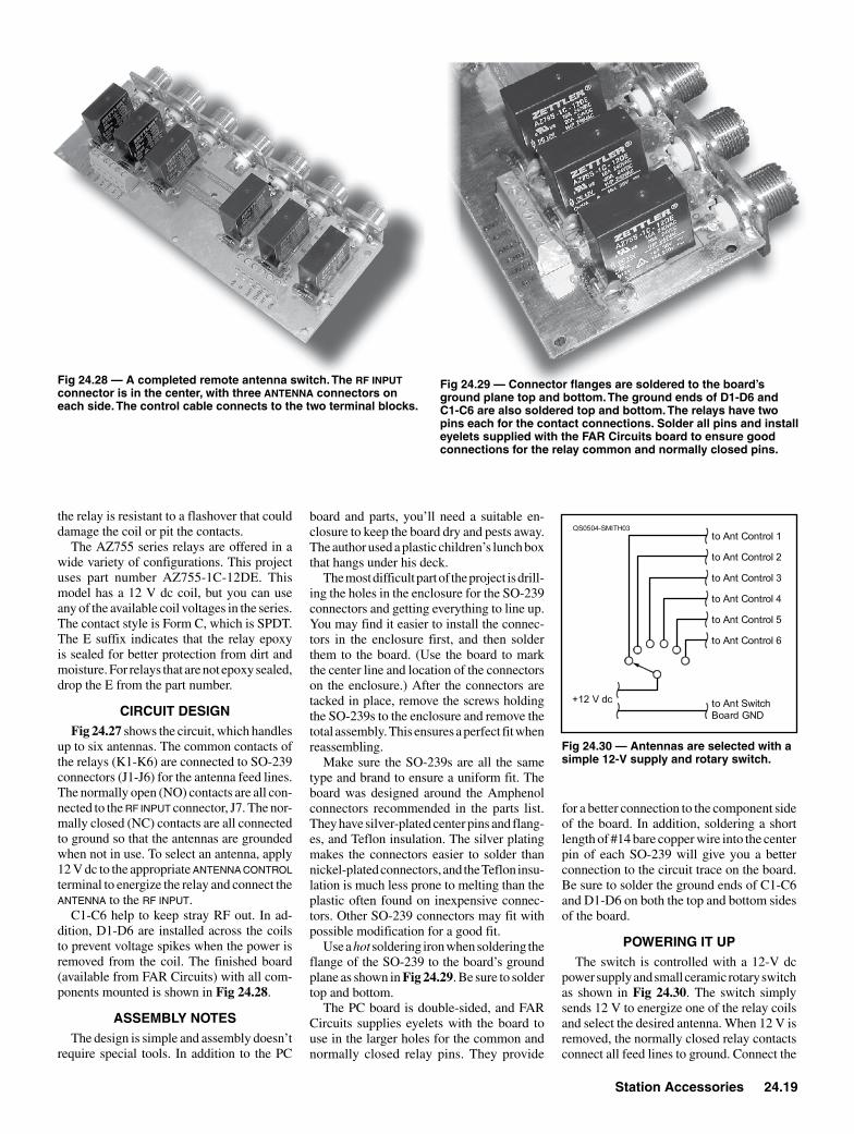
Station Accessories 24.19
the relay is resistant to a flashover that could damage the coil or pit the contacts.
The AZ755 series relays are offered in a wide variety of configurations. This project uses part number AZ755-1C-12DE. This model has a 12 V dc coil, but you can use any of the available coil voltages in the series. The contact style is Form C, which is SPDT. The E suffix indicates that the relay epoxy is sealed for better protection from dirt and moisture. For relays that are not epoxy sealed, drop the E from the part number.
CIRCUIT DESIGNFig 24.27 shows the circuit, which handles
up to six antennas. The common contacts of the relays (K1-K6) are connected to SO-239 connectors (J1-J6) for the antenna feed lines. The normally open (NO) contacts are all con-nected to the RF INPUT connector, J7. The nor-mally closed (NC) contacts are all connected to ground so that the antennas are grounded when not in use. To select an antenna, apply 12 V dc to the appropriate ANTENNA CONTROL terminal to energize the relay and connect the ANTENNA to the RF INPUT.
C1-C6 help to keep stray RF out. In ad-dition, D1-D6 are installed across the coils to prevent voltage spikes when the power is removed from the coil. The finished board (available from FAR Circuits) with all com-ponents mounted is shown in Fig 24.28.
ASSEMBLY NOTESThe design is simple and assembly doesn’t
require special tools. In addition to the PC
board and parts, you’ll need a suitable en-closure to keep the board dry and pests away. The author used a plastic children’s lunch box that hangs under his deck.
The most difficult part of the project is drill-ing the holes in the enclosure for the SO-239 connectors and getting everything to line up. You may find it easier to install the connec-tors in the enclosure first, and then solder them to the board. (Use the board to mark the center line and location of the connectors on the enclosure.) After the connectors are tacked in place, remove the screws holding the SO-239s to the enclosure and remove the total assembly. This ensures a perfect fit when reassembling.
Make sure the SO-239s are all the same type and brand to ensure a uniform fit. The board was designed around the Amphenol connectors recommended in the parts list. They have silver-plated center pins and flang-es, and Teflon insulation. The silver plating makes the connectors easier to solder than nickel-plated connectors, and the Teflon insu-lation is much less prone to melting than the plastic often found on inexpensive connec-tors. Other SO-239 connectors may fit with possible modification for a good fit.
Use a hot soldering iron when soldering the flange of the SO-239 to the board’s ground plane as shown in Fig 24.29. Be sure to solder top and bottom.
The PC board is double-sided, and FAR Circuits supplies eyelets with the board to use in the larger holes for the common and normally closed relay pins. They provide
Fig 24.29 — Connector flanges are soldered to the board’s ground plane top and bottom. The ground ends of D1-D6 and C1-C6 are also soldered top and bottom. The relays have two pins each for the contact connections. Solder all pins and install eyelets supplied with the FAR Circuits board to ensure good connections for the relay common and normally closed pins.
for a better connection to the component side of the board. In addition, soldering a short length of #14 bare copper wire into the center pin of each SO-239 will give you a better connection to the circuit trace on the board. Be sure to solder the ground ends of C1-C6 and D1-D6 on both the top and bottom sides of the board.
POWERING IT UPThe switch is controlled with a 12-V dc
power supply and small ceramic rotary switch as shown in Fig 24.30. The switch simply sends 12 V to energize one of the relay coils and select the desired antenna. When 12 V is removed, the normally closed relay contacts connect all feed lines to ground. Connect the
Fig 24.30 — Antennas are selected with a simple 12-V supply and rotary switch.
Fig 24.28 — A completed remote antenna switch. The RF INPUT connector is in the center, with three ANTENNA connectors on each side. The control cable connects to the two terminal blocks.

24.20 Chapter 24
PC board’s ground plane to a ground rod for lightning protection and as a means of elimi-nating static.
The control cable can be the 8-conductor variety usually used for rotators. Long runs of wire may require large conductors to prevent unacceptable voltage drops at the relay coils, but the relays will work over a fairly wide range of coil voltages so it’s not critical.
TESTINGInitial testing should be conducted on the
bench with an antenna analyzer or a trans-ceiver (internal antenna tuner off) and power/SWR meter connected to the RF INPUT jack.
Connect a 50 W load to one of the antenna jacks on the switch board. Apply a small of RF power. The SWR should be close to 1:1 (similar to readings without the switch in the line).
If everything looks okay, increase the pow-er and check the SWR through the switch on all bands that you plan to use it on. Next, move the wattmeter to the switch output and verify that the power on that side is about the same as the power at the input. There should be little or no measurable loss through the switch. Repeat these tests for all of the switch positions.
If you run an amplifier, test the switch at
high power. The author used the switch at 1-1.3 kW during normal intermittent opera-tion (SSB and CW) with no problems.
Although they are not designed for RF, the relays perform well. The board exhibits low SWR, low insertion loss and good isolation over a wide frequency range. The ARRL Lab tested the completed antenna switch board. Insertion loss measured <0.1 dB for 2- 50 MHz (for all ports to common). SWR mea-sured 1.1:1 or less from 2-28 MHz, 1.2:1 or less on 50 MHz. Isolation was >60 dB for 2-28 MHz, except for the two innermost ports, which were 50 dB at 28 MHz. Worst-case isolation on 50 MHz was 45 dB.
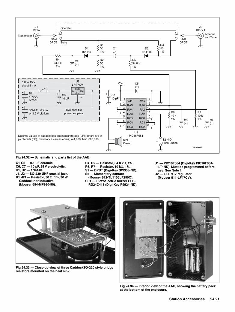
24.7 Audible Antenna BridgeThe audible antenna bridge (AAB) shown
in Fig 24.31 was designed by Rod Kreuter, WA3ENK. This project would help a visually impaired ham, but sighted hams will also find it very useful. (For example, tuning a mobile screwdriver antenna while you’re driving.) The AAB is rugged and easy to use, both in the harsh light of day and in the dark of night. It’s also inexpensive to build, and a kit is available.1
An absorptive type of SWR meter, the AAB is used to indicate how close the match is between your transmitter and your antenna. Its output is a tone whose pitch is propor-tional to SWR. It also sends the SWR value in Morse code.
Unlike most SWR meters on the market, this one actually absorbs power from your transmitter while you’re tuning, helping to protect your transmitter during tune-up. Many transmitters have SWR foldback capability and will decrease the output power if the an-tenna match is poor, but some do not.
By absorbing power in the AAB, no matter what you do at the antenna port, the trans-mitter never sees an SWR greater than 2:l. The trade-off is that 75% of your transmitter power ends up as heat in the bridge, so you need to switch out the AAB after you have tuned your antenna.
THEORY OF OPERATIONThe AAB works on a principle taken right
from the ARRL Antenna Book. The bridge consists of four impedances, or arms. See Fig 24.32. If three of the arms are 50 W resis-tors and the fourth is an antenna (or an antenna and tuner combination), then the bridge will be balanced when the antenna port is also 50 W. Diodes D1 and D2 sample the forward and reverse voltages, respectively. A periph-
Fig 24.31 — Front view of the audible antenna bridge.
eral interface controller (PIC) with a 10 bit analog to digital converter (A/D) digitizes these voltages and calculates the SWR.
The SWR is used to control a hardware pulse width modulator that produces the out-put tone. It’s also used by the Morse code routine to send the actual value of SWR, at 15 WPM with 5 WPM spacing.
The power that the AAB can handle during tune-up is a function of the resistors used in the three reference arms of the bridge. The 30 W noninductive resistors, R1-R3, are made by a
number of companies but are not cheap. The bridge resistors must be noninductive. Don’t use wire wound resistors!
Antenna tuning should be done with mini-mal power, and the AAB will work down to about 1 W. The 30 W resistors will handle tune-ups with about 60 W or perhaps 100 W for a short time. If you always remember to turn down your transmitter power, and you tune up quickly, the bridge resistors could be perhaps 5 W for normal rigs and 1 W for QRP rigs.
BUILDING THE AABA PC board is a nice way to build the AAB,
but you could easily construct such a simple circuit using ugly construction. Keep the wires short in the RF section. See Fig 24.33.
Use a heat sink for the noninductive resis-tors. Like many power devices, the power rating depends on getting the heat out! These resistors get really hot running at 10 or 20 W. See Fig 24.34. Use a big heat sink with heat sink compound, give yourself plenty of room in the cabinet and drill some holes to let the heat escape.
Switch S1 chooses TUNE/OPERATE and S2, the INQUIRE button, is used to report on various conditions, such as the SWR value in Morse code. You can eliminate the TUNE/OPERATE switch, but remember to remove the AAB from your feed line after tuning up.
To use the AAB in a QRP station, you may want to reduce resistors R4 and R5. They are sized so that a 25 W transmitter will not saturate the analog to digital converter (ADC) on the PIC when using fresh batteries (more on this later). A good value for a 5 W trans-mitter would be about 20 kW. So long as the voltages at pin 12 and pin 13 of U1 are below the battery voltage, the system will work fine.
Station Accessories 24.21
Fig 24.32 — Schematic and parts list of the AAB.
C1-C5 — 0.1 µF ceramic.C6, C7 — 10 µF, 25 V electrolytic.D1, D2 — 1N4148.J1, J2 — SO-239 UHF coaxial jack.R1 -R3 — Resistor, 50 W, 1%, 30 W
Caddock noninductive (Mouser 684-MP930-50).
R4, R5 — Resistor, 34.8 kW, 1%.R6, R7 — Resistor, 10 kW, 1%.S1 — DPDT (Digi-key SW333-ND).S2 — Momentary contact
(Mouser 612-TL1105LF250Q).SP1 — Piezoelectric buzzer EFB-
RD24C411 (Digi-key P9924-ND).
U1 — PIC16F684 (Digi-key PIC16F684-1/P-ND). Must be programmed before use. See Note 1.
U2 — LF4.7CV regulator (Mouser 511-LF47CV).
Fig 24.33 — Close-up view of three CaddockTO-220 style bridge resistors mounted on the heat sink.
Fig 24.34 — Interior view of the AAB, showing the battery pack at the bottom of the enclosure.

24.22 Chapter 24
POWERING THE AABTo save power the AAB uses a sleep mode.
If you haven’t pushed the INQUIRE button for about 5 minutes, the AAB will go to sleep after sending the letter N for “night night.” During sleep the current draw is about 2 µA. Pushing the switch while it’s sleeping will wake up the AAB and it will send the letter U (“up”).
The first four prototypes used four AAA batteries and a low-dropout 4.7 V regulator. This made for a nice stiff supply and very good battery life, with only one problem. Even though the PIC uses less than 2 µA during sleep, the regulator uses 500 µA. Bat-tery data says that alkaline AA batteries will last 6 months at this level and AAA batteries about half that long. Consider adding an ON/
OFF switch if you go this route.The other option is to use batteries without
a regulator. Normally you couldn’t get away with this without providing a separate voltage reference for the ADC in the PIC. In this case it doesn’t matter as much because SWR is a ratio of two voltages.
What does matter is the battery voltage with respect to the voltage produced by the RF signal. Diodes D1 and D2 rectify the RF and produce a dc voltage proportional to RF power. This voltage is divided by resistors R4, R6 and R5, R7. The voltage at the ADC inputs of the PIC, pins 12 and 13, must be less than the power supply voltage. With a regulated supply this isn’t much of a problem and if you’re careful it can also work with unregulated batteries.
Microchip recommends that these parts be run on 2.5 to 5.5 V if you need the 10 bit ADC to be accurate. Many battery combinations will provide this, but consider lithium bat-teries instead of alkaline. The voltage from an alkaline battery begins to fall very early in its life and continues at a downward slope until it is exhausted. A lithium battery, on
the other hand, provides a nearly constant voltage throughout its useful life. A 3.6 V AA size lithium should last a few years, but with the lower output voltage you may want to reduce R4 and R5. The final proto-type used three AAA lithium batteries (each about 1.7 V when new), with no regulator or ON/OFF switch, which should last at least two years.
U1’s ADC converter will saturate at some level. With new batteries, let’s say this level is 25 W when the power supply is 4.5 V. When the power supply has fallen to 3.5 V, the RF level that will saturate the converter will be 15 W. So if you find that the output of your rig, which used to be fine, is now saturating the ADC, it’s time to change batteries.
USING THE AABConnect your transmitter to the INPUT and
your antenna/tuner to the OUTPUT. Turn your transmit power down to 5 or 10 W and put S1 in the TUNE position. Wake the AAB up by pushing the INQUIRE button. Key your trans-mitter in a mode with some carrier power. The AAB should start to produce a steady tone. Adjust your tuner or antenna for the lowest tone pitch. Press the INQUIRE button for the numeric SWR value.
When the AAB is operating normally, it produces a tone proportional to SWR. The tone ranges from 250 Hz at an SWR of 1.0:1, rising to 4450 Hz at an SWR of about 15:1. Errors can occur and at times the AAB can’t make a measurement. If an error occurs, either a high pitched tone or no tone is produced. Pushing the INQUIRE button will give you more information. Five different conditions can occur:
Normal operation. A tone proportional to SWR is produced. Press INQUIRE and a two digit SWR value is sent separated by the letter R (Morse for the decimal point character).
Error 1. The forward power is too low for a reliable measurement. No tone is produced. INQUIRE button sends letter L (low).
Error 2. Forward power is too high (al-most saturating the ADC). A pulsing tone proportional to SWR is produced. However, if the ADC is saturated this value might be meaningless. INQUIRE button sends letter S (saturated).
Error 3. SWR is greater than 9.9:1. A tone proportional to SWR is produced. INQUIRE button sends letter H (high).
Error 4. The reverse voltage is greater than the forward voltage. Two things can cause this error. You might be near a high power transmitter, or you connected the transmit-ter to the output port. No tone is produced. INQUIRE button sends letter F (fault).
The PIC used in this design could be used in a more standard SWR meter, such as those with a transformer type sensor. As long as the meter produces a forward and reverse voltage that you can scale to be from 0 to 3 up to 5 V (depending on your power supply choice), it will work just fine. However, the driving im-pedance of the voltage must be 10 kW or less.
The author thanks the Ham Radio Com-mittee of the National Federation of the Blind for inspiration, and Tom Fowle, WA6IVG, and Bill Gerrey, WA6NPC, of the Smith-Kettlewell Research Institute for testing proto types.
1A kit of parts including a printed circuit board is available from Q-Sat, 319 McBath St, State College, PA 16801. The price is currently $30, postpaid. PC boards are available for $7 postpaid and a programmed PIC is available for $6 postpaid. Source code for an unprogrammed PIC is available on the ARRL Web site. Go to www.arrl.org/qst-in-depth and look for Kreuter0607.zip in the 2007 section.
24.8 A Trio of Transceiver/Computer InterfacesVirtually all modern Amateur Radio trans-
ceivers (and many general-coverage receiv-ers) have provisions for external computer control. Most hams take advantage of this feature using software specifically developed for control, or primarily intended for some other purpose (such as contest logging), with rig control as a secondary function.
Unfortunately, the serial port on most ra-dios cannot be directly connected to the serial port on most computers. The problem is that most radios use TTL signal levels while most computers use RS-232-D.
The interfaces described here simply con-vert the TTL levels used by the radio to the RS-232-D levels used by the computer, and
vice versa. Interfaces of this type are often referred to as level shifters. Two basic de-signs, one having a couple of variations, cover the popular brands of radios. This article, by Wally Blackburn, AA8DX, first appeared in February 1993 QST.
TYPE ONE: ICOM CI-VThe simplest interface is the one used for
the ICOM CI-V system. This interface works with newer ICOM and Ten-Tec rigs. Fig 24.35 shows the two-wire bus system used in these radios.
This arrangement uses a CSMA/CD (car-rier-sense multiple access/collision detect) bus. This refers to a bus that a number of
stations share to transmit and receive data. In effect, the bus is a single wire and common ground that interconnect a number of radios and computers.
The single wire is used for transmitting and receiving data. Each device has its own unique digital address. Information is transferred on the bus in the form of packets that include the data and the address of the intended receiv-ing device.
The schematic for the ICOM/Ten-Tec in-terface is shown in Fig 24.36. It is also the Yaesu interface. The only difference is that the transmit data (TxD) and receive data (RxD) are jumpered together for the ICOM/Ten-Tec version.

Station Accessories 24.23
The signal lines are active-high TTL. This means that a logical one is represented by a binary one (+5 V). To shift this to RS-232-D it must converted to –12 V while a binary zero (0 V) must be converted to +12 V. In the other direction, the opposites are needed: –12 V to +5 V and +12 V to 0 V.
U1 is used as a buffer to meet the inter-face specifications of the radio’s circuitry and provide some isolation. U2 is a 5-V-powered RS-232-D transceiver chip that translates be-tween TTL and RS-232-D levels. This chip uses charge pumps to obtain ±10 V from a single +5-V supply. This device is used in all three interfaces.
A DB25 female (DB25F) is typically used at the computer end. Refer to the discussion of RS-232-D earlier in the chapter for 9-pin connector information. The interface con-nects to the radio via a 1⁄8-inch phone plug. The sleeve is ground and the tip is the bus connection.
Fig 24.35 — The basic two-wire bus system that ICOM and newer Ten-Tec radios share among several radios and computers. In its simplest form, the bus would include only one radio and one computer.
Fig 24.36 — ICOM/Ten-Tec/Yaesu interface schematic. The insert shows the ICOM/Ten-Tec bus connection, which simply involves tying two pins together and eliminating a bypass capacitor.
C7-C10 — 0.01-µF ceramic disc. U1 — 7417 hex buffer/driver. U2 — Harris ICL232 or Maxim MAX232.
It is worth noting that the ICOM and Ten-Tec radios use identical basic command sets (although the Ten-Tec includes additional commands). Thus, driver software is com-patible. The manufacturers are to be com-mended for working toward standardizing these interfaces somewhat. This allows Ten-Tec radios to be used with all popular software that supports the ICOM CI-V interface. When configuring the software, simply indicate that an ICOM radio (such as the IC-735) is con-nected.
TYPE TWO: YAESU INTERFACEThe interface used for Yaesu rigs is iden-
tical to the one described for the ICOM/Ten-Tec, except that RxD and TxD are not jumpered together. Refer to Fig 24.36. This ar-rangement uses only the RxD and TxD lines; no flow control is used.
The FT-990 and FT-1000/FT-1000D use an emitter follower as the TTL output. If the input
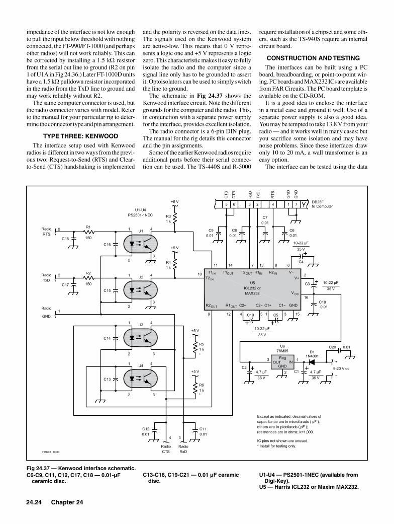
24.24 Chapter 24
impedance of the interface is not low enough to pull the input below threshold with nothing connected, the FT-990/FT-1000 (and perhaps other radios) will not work reliably. This can be corrected by installing a 1.5 kW resistor from the serial out line to ground (R2 on pin 1 of U1A in Fig 24.36.) Later FT-1000D units have a 1.5 kW pulldown resistor incorporated in the radio from the TxD line to ground and may work reliably without R2.
The same computer connector is used, but the radio connector varies with model. Refer to the manual for your particular rig to deter-mine the connector type and pin arrangement.
TYPE THREE: kENWOODThe interface setup used with Kenwood
radios is different in two ways from the previ-ous two: Request-to-Send (RTS) and Clear-to-Send (CTS) handshaking is implemented
and the polarity is reversed on the data lines. The signals used on the Kenwood system are active-low. This means that 0 V repre-sents a logic one and +5 V represents a logic zero. This characteristic makes it easy to fully isolate the radio and the computer since a signal line only has to be grounded to assert it. Opto isolators can be used to simply switch the line to ground.
The schematic in Fig 24.37 shows the Kenwood interface circuit. Note the different grounds for the computer and the radio. This, in conjunction with a separate power supply for the interface, provides excellent isolation.
The radio connector is a 6-pin DIN plug. The manual for the rig details this connector and the pin assignments.
Some of the earlier Kenwood radios require additional parts before their serial connec-tion can be used. The TS-440S and R-5000
require installation of a chipset and some oth-ers, such as the TS-940S require an internal circuit board.
CONSTRUCTION AND TESTINGThe interfaces can be built using a PC
board, breadboarding, or point-to-point wir-ing. PC boards and MAX232 ICs are available from FAR Circuits. The PC board template is available on the CD-ROM.
It is a good idea to enclose the interface in a metal case and ground it well. Use of a separate power supply is also a good idea. You may be tempted to take 13.8 V from your radio — and it works well in many cases: but you sacrifice some isolation and may have noise problems. Since these interfaces draw only 10 to 20 mA, a wall transformer is an easy option.
The interface can be tested using the data
Fig 24.37 — kenwood interface schematic.C6-C9, C11, C12, C17, C18 — 0.01-µF
ceramic disc.C13-C16, C19-C21 — 0.01 µF ceramic
disc.U1-U4 — PS2501-1NEC (available from
Digi-key).U5 — Harris ICL232 or Maxim MAX232.

Station Accessories 24.25
in Tables 24.6, 24.7 and 24.8. Remember, all you are doing is shifting voltage levels. You will need a 5-V supply, a 9-V battery and a voltmeter. Simply supply the voltages as described in the corresponding table for your interface and check for the correct voltage on the other side. When an input of –9 V is called for, simply connect the positive terminal of the battery to ground.
During normal operation, the input signals
Table 24.6kenwood Interface TestingApply ResultGND to Radio-5 –8 to –12 V at PC-5+5 V to Radio-5 +8 to +12 V at PC-5+9 V to PC-4 +5 V at Radio-4–9 V to PC-4 0 V at Radio-4GND to Radio-2 –8 to –12 at PC-3+5 V to Radio-2 +8 to +12 V at PC-3+9 V to PC-2 +5 V to Radio-3–9 V to PC-2 0 V at Radio-3
Table 24.8Yaesu Interface TestingApply ResultGND to Radio TxD +8 to +12 V at PC-3+5 V to Radio TxD –8 to –12 V at PC-3+9 V to PC-2 0 V at Radio RxD–9 V to PC-2 +5 V at Radio RxD
Table 24.7ICOM/Ten-Tec Interface TestingApply ResultGND to Bus +8 to +12 V at PC-3+5 V to Bus –8 to –12 V at PC-3–9 V to PC-2 +5 V on Bus+9 V to PC-2 0 V on Bus
to the radio float to 5 V because of pullup resistors inside the radio. These include RxD on the Yaesu interface, the bus on the ICOM/Ten-Tec version, and RxD and CTS on the Kenwood interface. To simulate this during testing, these lines must be tied to a 5-V supply through 1-kW resistors. Connecting these to the supply without current-limiting resistors will damage the interface circuitry. R5 and R6 in the Kenwood schematic illustrate this. They are not shown (but are still needed) in
the ICOM/Ten-Tec/Yaesu schematic. Also, be sure to note the separate grounds on the Kenwood interface during testing.
Another subject worth discussing is the ra-dio’s communication configuration. The serial ports of both the radio and the computer must be set to the same baud rate, parity, and num-ber of start and stop bits. Check your radio’s documentation and configure your software or use the PC-DOS/MS-DOS MODE command as described in the computer manual.
24.9 A Simple Serial InterfaceA number of possibilities exist for building
an RS-232-to-TTL interface level converter to connect a transceiver to a computer serial port. The interface described here by Dale Botkin, NØXAS, is extremely simple, requiring only a few common parts.
Most published serial interface circuits fall into one of the following categories:
• Single chip, MAX232 type. These are relatively expensive, require several capaci-tors, take up lots of board space and usually require ordering parts.
• Single chip, MAX233 type. This version doesn’t need capacitors. Otherwise it shares most of the characteristics of the MAX232 type device, but is even more expensive.
• Transistors. Usually transistor designs use a mix of NPN and PNP devices, four to eight or more resistors, and usually capacitors and diodes. This is just too many parts!
• Other methods. Some designs use series resistors, or TTL logic inverters with resistors. The idea is that the voltages may be out of specification for the chip, but if the current is low enough it won’t damage the device. This is not always safe for the TTL/CMOS device. With just a series resistor the serial data doesn’t get inverted, so it requires the use of a software USART. It can work, but it’s far from ideal.
A SIMPLER APPROACHThe EIA-232 specification specifies a
Fig 24.38 — Schematic for the simple serial interface.J1 — DB9F or connector to fit device
serial port. Note that pin assignments for RxD, TxD and RTS are different on DB25 connectors.
Q1, Q2 — Small signal MOSFET, 2N7000 or equiv.
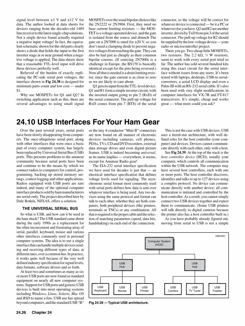
24.26 Chapter 24
signal level between ±3 V and ±12 V for data. The author looked at data sheets for devices ranging from the decades-old 1489 line receiver to the latest single-chip solutions. Not a single device found actually required a negative input voltage! In fact, the equiva-lent schematic shown for the old parts clearly shows a diode that holds the input to the first inverter stage at or near ground when a nega-tive voltage is applied. The data sheets show that a reasonable TTL-level input will drive these devices perfectly well.
Relieved of the burden of exactly repli-cating the PC-side serial port voltages, the interface shown in Fig 24.38 is designed for minimum parts count and low cost — under $1.
Why use MOSFETs for Q1 and Q2? In switching application such as this, there are several advantages to using small signal
MOSFETs over the usual bipolar choices like the 2N2222 or 2N3904. First, they need no base current limiting resistors — the MOS-FET is a voltage operated device, and the gate is isolated from the source and drainch The gate on a 2N7000 is rated for ±20 V, so you don’t need a clamping diode to prevent nega-tive voltages from reaching the gate. They can also be had just as cheaply as their common bipolar cousins. (If sourcing 2N7000s is a challenge in Europe, the BS170 is basically identical except for the pins being reversed.) Now all that is needed is a drain limiting resis-tor, since the gate current is as close to zero as we are likely to care about.
Q1 gets its input from the TTL-level device. Q1 and R1 form a simple inverter circuit, with the inverted output going to pin 2 (RxD) of the serial connector. The pull-up voltage for RxD comes from pin 7 (RTS) of the serial
connector, so the voltage will be correct for whatever device is connected — be it a PC or whatever else you have. Q2 and R2 are another inverter, driven by TxD from pin 3 of the serial connector. The pull-up voltage for R2 should be supplied by the low-voltage device — your radio or microcontroller project.
There you go. Two cheap little MOSFETs, two resistors. The 2.2 kW, 1⁄4 W resistors, seem to work with every serial port tried so far. The author has sold several hundred kits using this exact circuit for the serial inter-face without issues from any users. It’s been tested with laptops, desktops, USB-to serial-converters, a serial LCD display and even a Palm-III with an RS-232 serial cable. It’s also been used with very slight modifications in computer interfaces for VX-7R and FT-817 transceivers. It’s simple, cheap and works great — what more could you ask?
24.10 USB Interfaces For Your Ham GearOver the past several years, serial ports
have been slowly disappearing from comput-ers. The once-ubiquitous serial port, along with other interfaces that were once a basic part of every computer system, has largely been replaced by Universal Serial Bus (USB) ports. This presents problems to the amateur community because serial ports have been and continue to be the means by which we connect radios to computers for control, pro-gramming, backing up stored memory set-tings, contest logging and other applications. Radios equipped with USB ports are rare indeed, and many of the optional computer interface products sold by ham manufacturers are serial-only. The project described here by Dale Botkin, NØXAS, offers a solution.
THE UNIVERSAL SERIAL BUSSo what is USB, and how can it be used in
the ham shack? The USB standard came about during the early 1990s as a replacement for the often inconvenient and frustrating array of serial, parallel, keyboard, mouse and various other interfaces commonly used in personal computer systems. The idea is to use a single interface that can handle multiple devices send-ing and receiving different types of data, at different rates, over a common bus. In practice, it works quite well because of the very well defined industry specification for signal levels, data formats, software drivers and so forth.
At least two and sometimes as many as six or more USB ports are now found as standard equipment on nearly all new computer sys-tems. Support for USB ports and generic USB devices is built into most operating systems including Windows, Linux, Solaris, Mac OS and BSD to name a few. USB use has spread beyond computers, and the standard USB “B” Fig 24.39 — Typical USB architecture.
or the tiny 4-conductor “Mini B” connectors are now found on all manner of electronic devices including cameras, cell phones, PDAs, TVs, CD and DVD recorders, external data storage drives and even digital picture frames. USB is indeed becoming universal, as its name implies — everywhere, it seems, except for Amateur Radio gear!
The EIA-232 serial interface specification we have used for decades is just that — an electrical interface specification that defines voltage levels used for signaling. The asyn-chronous serial format most commonly used with serial ports defines how data is sent over whatever interface is being used. Any two de-vices using the same protocol and format can talk to each other, whether they are both com-puters, both peripheral devices (like printers, terminals or TNCs) or any combination. All that is required is the proper cable and the selec-tion of matching parameters (speed, data bits, handshaking) on each end of the connection.
This is not the case with USB devices. USB uses a tiered-star architecture, with well de-fined roles for the host controller (your com-puter) and devices. Devices cannot communi-cate directly with each other, only with a host.
See Fig 24.39. At the top of the stack is the host controller device (HCD), usually your computer, which controls all communication within the USB network. The computer may have several host controllers, each with one or more ports. The host controller discovers, identifies and talks to up to 127 devices using a complex protocol. No device can commu-nicate directly with another device; all com-munication is initiated and controlled by the host controller. As a result, you cannot simply connect two USB devices together and expect them to communicate. (Some USB printers will talk directly to digital cameras because the printer also has a host controller built in.)
As you have probably already figured out, moving from serial to USB is not a simple

Station Accessories 24.27
matter of converting voltage levels or even data formats. USB devices all need some embedded “smarts,” usually in the form of either a dedi-cated USB interface chip or a microcontroller using firmware to talk to the USB host. Where we could once use simple transistor circuits to adapt RS-232 serial to the TTL voltage levels used by many radios, we now must add the complete USB interface into the picture.
The USB specification is freely available and well documented, and there are books dealing with designing the software to use the interface. If you’re starting from scratch it is a very daunting task to even understand exactly how USB works, let alone design and build your own USB-equipped device. If you’re willing and dedicated enough, you can imple-ment your own USB device using a fairly broad range of available microcontrollers. There are also dedicated function chips that implement a complete USB interface — or parts of it — in one or two devices.
Fortunately, several manufacturers have stepped up to make using USB relatively easy for the experimenter. One of the most com-monly used solutions is from Future Tech-nology Devices International (FTDI). FTDI manufactures a line of USB interface chips that plug into the Universal Serial Bus on one side and present a serial or parallel interface on the other side. The chips are quite versatile and are commonly used to add USB functionality to a wide range of devices ranging from cell phones to USB-to-serial cables. They are also available in several forms such as plug-in modules with a USB connector and the interface logic, all on a small PC board with pins that can be plugged into a standard IC socket.
CONSTRUCTIONThis project uses an FT232R series chip
from FTDI to bridge the USB interface from your computer to a TTL-level serial interface that can be adapted to use with many different ham rigs. The chip has built-in logic to handle the USB interface, respond to queries and commands from the computer, and send and receive serial data. By using special drivers available from FTDI (and built into Windows and many other systems), it can appear to your programs as a standard serial COM port.
Once the conversion to serial data is done, all that remains is to adapt the signals to the particular interface used by your equipment. In many cases, this serial data can simply be connected directly to the rig using the ap-propriate connector. In others it may require some extra circuitry to accommodate vari-ous interface schemes used by manufacturers. The most common is an open-collector bus type interface, which is easily accommodated using a few inexpensive parts.
Construction of this project can be handled in a couple of different ways. The FT232R series chips are available from various sup-
pliers at low cost. Unfortunately they are only available in SSOP and QFLP surface mount packages that can be difficult to work with unless you use a custom printed circuit board. (An additional letter is tacked onto the part number to identify the package. For example, the FT232RL uses a 28-pin SSOP package.) There are SSOP-to-through-hole adapter boards available, but they are relatively ex-pensive and still require some fine soldering.
Fortunately FTDI also sells a solution in the form of the TTL-232R (Fig 24.40). It incor-porates a USB “A” connector, an FT232RQ chip and the required power conditioning on a tiny PCB encapsulated in plastic, all about the size of a normal USB connector. A 6-ft long cable terminates in a 6-position inline header that provides ground, +5 V, and TTL level TxD, RxD, RTS and CTS signals.
You can connect these signals directly to your own microprocessor projects and have an “instant” USB connection. You can also build a variety of interface cables or boards for use with different radios. This arrangement is ideal for the experimenter and the person who might need several different interfaces for use with several different rigs — like many of us! The cost of the TTL-232R cable is quite reasonable, in fact lower than the cost of having a prototype PCB made to build your own equivalent device. Of course that option is still available to those who need more flexibility.
USING USB IN THE SHACkWith the USB-to-serial conversion handled
so easily, the only remaining task is to adapt the TTL-level serial interface of the FT232R to the interface used by your particular radio. In the case of some rigs, such as the Yaesu FT-817, Kenwood TM-G707A and many oth-ers, it’s simply a matter of wiring up the right connector, as shown in Fig 24.41.
For communicating with individual ICOM and Ten-Tec rigs, one simple solution is to simply connect the transmit and receive data signals together and wire up a 1⁄8-inch stereo plug as shown in Fig 24.42. This will work with a single device connected, but lacks the open-collector drivers needed to be compatible with attaching multiple devices to the CI-V bus.
Fig 24.40 — The FTDI TTL-232R cable simplifies construction.
Fig 24.41 — Using the FTDI USB-to-serial interface with some radios is as simple as wiring up a connector. Connections for the Yaesu FT-817 are shown at A, the kenwood TM-G707A (PG-4 type) at B, and kenwood hand-helds (PG-5 type) at C. Ground, RxD and TxD connections are made to the 6-pin connector on the TTL-232R cable.
Fig 24.42 — The transmit and receive data signals can be connected together for use with a single Ten-Tec or ICOM CI-V device.
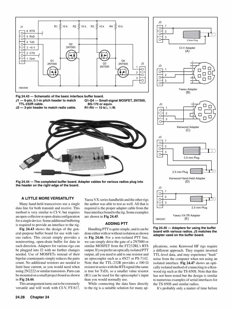
24.28 Chapter 24
A LITTLE MORE VERSATILITYMany hand-held transceivers use a single
data line for both transmit and receive. This method is very similar to CI-V, but requires an open-collector or open-drain configuration for a single device. Some additional buffering is required to provide an interface to the rig.
Fig 24.43 shows the design of the gen-eral-purpose buffer board for use with vari-ous radios. This circuit simply provides a noninverting, open-drain buffer for data in each direction. Adapters for various rigs can be plugged into J2 with no further changes needed. Use of MOSFETs instead of their bipolar counterparts simply reduces the parts count. No additional resistors are needed to limit base current, as you would need when using 2N2222 or similar transistors. Parts can be mounted on a small project board as shown in Fig 24.44.
This arrangement turns out to be extremely versatile and will work with CI-V, FT-817,
Fig 24.43 — Schematic of the basic interface buffer board.J1 — 6-pin, 0.1-in pitch header to match
TTL-232R cable.J2 — 3-pin header to match radio cable.
Q1-Q4 — Small-signal MOSFET, 2N7000, BS-170 or equiv.
R1-R4 — 10 kW, 1⁄4 W.
Fig 24.44 — The completed buffer board. Adapter cables for various radios plug into the header on the right edge of the board.
Fig 24.45 — Adapters for using the buffer board with various radios. J3 matches the adapter used on the buffer board.
Yaesu VX-series handhelds and the other rigs the author was able to test as well. All that is required is the proper adapter cable from the base interface board to the rig. Some examples are shown in Fig 24.45.
ADDING PTTHandling PTT is quite simple, and it can be
done either with or without isolation as shown in Fig 24.46. For a non-isolated PTT line, we can simply drive the gate of a 2N7000 or similar MOSFET from the FT232RL’s RTS output. If you prefer an optically isolated PTT output, all you need to add is one resistor and an optocoupler such as a 4N27 or PS-7142. Note that the TTL-232R provides a 100 W resistor in series with the RTS signal (the same is true for TxD), so a smaller value resistor (R1) can be used for the optocoupler’s input than you would normally use.
While connecting the data lines directly to the rig is a suitable solution for many ap-
plications, some Kenwood HF rigs require a different approach. They require inverted TTL-level data, and may experience “hash” noise from the computer when not using an isolated interface. Fig 24.47 shows an opti-cally isolated method of connecting to a Ken-wood rig such as the TS-850S. Note that this has not been tested but the design is similar to numerous examples of serial interfaces for the TS-850S and similar radios.
It’s probably only a matter of time before

Station Accessories 24.29
Fig 24.46 — PTT can be added either without isolation (A) or with an optoisolator (B).
Fig 24.47 — Isolated kenwood interface for the TS-850S and similar HF transceivers requiring inverted TTL-level data and isolated lines.
we start seeing the tiny USB “Mini B” con-nector appear on new ham gear. It has become inexpensive and easy to add USB to pretty much any product, and as serial ports become more and more rare the manufacturers will eventually face overwhelming consumer de-mand to switch. In the meantime, you can do a little homebrewing and use your new, serial port free computer to talk to all of your ham gear for very little cost.
24.11 The Universal keying AdapterWhen Dale Botkin, NØXAS, was about
to start restoring his old Heathkit HW-16, he decided it was time to explore what would be needed to key this tube rig using an electronic keyer. He also remembered — not fondly — having been “bitten” a few times when he touched metal parts of the key. There was some substantial voltage on the key, and he wanted to avoid touching it againch The key jack of this rig has a negative voltage, some-thing like –85 V or more. Even the 2N7000 output of a solid-state keyer, rated at 60 V, would be no match for that. The Universal Keying Adapter (UKA) shown in Fig 24.48 bridges the gap between a modern keyer and a classic tube-type transmitter, and it can also be used to key older tube-type amplifier TR switching lines with solid-state transceivers that can’t handle the voltage or current re-quirements.
kEYING SCHEMESOlder gear generally uses one of two keying
Fig 24.48 — This version of the Universal keying Adapter 2 is available as a kit from www.hamgadgets.com. Parts count is low, and it can easily be built on a small project board.

24.30 Chapter 24
schemes, grid-block or cathode keying. Grid-block keying requires that your key handle fairly high negative bias voltages, often in the 150 V range. Cathode keying is more demanding, with voltages up to +350 V or so. Most modern solid state keyers use a simple transistor output circuit suitable only for low-voltage, positive keying. Obviously, neither grid-block nor cathode keyed transmitters should be connected to such an output! At the very least it’s going to damage the keyer.
Most grid-block keying adapters use one or two bipolar transistors and are designed specifically to key grid-block rigs. This is fine as far as it goes, but also requires that you have one setup for solid state rigs, another for grid-blocked rigs, and still another if you have a cathode keyed boat anchor as well. It’s not an optimum solution. Of course one could use a relay to key just about anything, but relay contact noise would quickly get really irritat-ing. Relays also eventually wear out, contacts get dirty and the coils can use quite a bit of current, meaning battery powered keyers will suffer from very limited battery life.
Solid-State RelaysSolid state relays exist, but they can be
expensive. The author finally hit upon what seems to be an ideal solution. It’s cheap, small, relatively low current, uses low voltage control and is capable of switching fairly high ac or dc voltages. Perfect! Crydom, NEC, Fairchild, Omron and other manufacturers make very similar small, inexpensive MOS-FET solid state relays. Suitable model num-bers include the NEC PS7142 and PS7342, Fairchild HSR412, Omron G3VM-401B and others. Depending on the part selected they can handle up to a couple hundred milli-amps and will switch up to 400 V ac or dc. All of this in a 6-pin DIP form factor, and for just a few bucks!
The MOSFET solid-state relay (SSR) is very similar to an optoisolator, but somewhat more versatile. Ac or dc loads can be switched, and the allowable load voltages are much higher than regular optoisolators. Driving the relay input involves supplying a few mA of current to turn on an LED inside the device. This requires about 1.4 V at a recommended forward current of 10 to 30 mA. The output is a pair of MOSFETs with common sources and a photo gate rather than a hard-wired gate. Turn on the LED and the MOSFETs conduct, turn off the LED and the MOSFETs shut off. Just like a relay, it’s simple and elegant.
kEYING ADAPTER CIRCUITSFor a simple keying adapter arrangement,
all that is needed is the MOSFET solid-state relay, one resistor, and a dc power source such as a battery. See Fig 24.49. The keying input from your hand key or electronic keyer completes the input circuit through the cur-
rent limiting resistor and the input side of the SSR, turning the output on. In this example, the value of R1 is determined using Ohm’s Law to give between 10 and 30 mA of current at the desired input voltage. For example, for use with two AA alkaline batteries, a range of 100 to 300 W is okay; 150 or 220 W will work reliably with NiCd or NiMH cells as well. If you plan to use a 13.8 V dc power supply, a 1 kW resistor should be fine for R1.
It soon became apparent that other uses existed in addition to just isolating the key or keyer from a transmitter. The addition of a simple transistor inverter allows the use of
computer keying in parallel with input from a straight key, bug or keyer. This is handy, for example, to contesters using computers for keying who may need to send some informa-tion by hand from time to time. See Fig 24.50. The use of a 2N7000 MOSFET instead of the common NPN transistor makes it easier to accommodate both serial and parallel port use, since the gate will withstand up to 20 V positive or negative and does not need to be current limited. In this example, the value of R1 should be determined as mentioned earlier. R2’s purpose is to keep the MOSFET gate from floating, so its value is not critical but
Fig 24.50 — The Universal keying Adapter circuit with provisions for using computer keying in parallel with a hand key or keyer. Two methods of increasing the load current capacity are shown at B and C (see text for discussion).
Fig 24.49 — The original Universal keying Adapter circuit used a solid-state relay and a battery for power.
k1 — Optically coupled solid-state relay, Fairchild HSR412 or equivalent.
R1 — 1⁄4 W resistor, varies with supply
voltage (see text). Use 150 or 220 W for two AA cells; 1 kW for 13.8 V dc power source.
k1 — Optically coupled solid-state relay, Fairchild HSR412 or equivalent.
R1 — 1⁄4 W resistor, varies with supply
voltage (see text). Use 150 or 220 W for two AA cells; 1 kW for 13.8 V dc power source.

Station Accessories 24.31
10 kW or 100 kW are good values.The design eventually evolved to include a
full-wave bridge rectifier allowing either ac or dc input, a Zener diode for voltage regulation and an LED keying indicator. The result was the Universal Keying Adapter 2, which is also available in kit form (see www.hamgad-gets.com). The UKA-2 can accept any dc or ac power source up to about 30 V, and is adaptable to lower power battery operation by substituting or eliminating some of the power supply parts.
OTHER CONFIGURATIONSIt is worth noting that if only positive or
only negative voltages will be used, the out-put current capacity can be greatly increased and the on-state resistance greatly decreased by connecting the two MOSFET drain out-puts in parallel rather than serial. An ex-ample of this is shown in Fig 24.50B. For the HSR412, maximum load current increas-
es from 140 mA for series output to 210 mA for parallel. An added feature of this arrangement is the presence of the in-trinsic “body diodes” of the MOSFETS. If you are keying an amp that has an internal keying relay, this can serve to absorb some of the back EMF when the relay releases. Note that this arrangement requires that pin 5 of the IC be at a lower voltage than the other two pins — in other words, ground for positive keying, or –V for negative keying. Since the output is completely isolated from the input, the polarity of the output connector can be changed without the risk of exposing your other gear to dangerous voltages.
Although the IC solid-state relays are good for a wide range of uses, there are ap-plications that present more of a load than the device is able to safely handle even with the outputs in parallel. For loads of more than the rated device current, an external
MOSFET switch can be used. Again, the resulting output is optically isolated from the input. Resistor R3 shown in Fig 24.50C keeps the gate of the 2N7000 MOSFET low until the input is activated, so its value is not critical. The gate voltage +V needs only to be within the safe range for the device selected; in most cases 12 V will do fine.
The UKA design works well with both grid-block and cathode keyed rigs, as well as solid state. It’s been tested with a TS-930SAT, Heath HW-16, FT-817, Rock-Mites, FT-480R and more. It has also been used with cathode keyed rigs such as the Heath DX-40, and many more examples of this circuit are in use keying various “boat anchor” rigs and amps. It works quite well to key older tube power amplifiers with solid-state transceivers that are not equipped with suitable keying relays or circuits. The input works well with any rig, key, electronic keyer, serial or parallel port tried so far.
24.12 The TiCk-4 — A Tiny CMOS keyerTiCK stands for “Tiny CMOS Keyer” and
this is the fourth version of the chip. It is based on an 8-pin DIP microcontroller from Microchip Corporation, the PIC12CE674. This IC is a perfect candidate for all sorts of Amateur Radio applications because of its small size and high performance capabilities. This project originally used the TiCK-2 chip (based on the PIC12C509) and was described fully in Oct 1997 QST by Gary M. Diana, Sr, N2JGU, and Bradley S. Mitchell, WB8YGG. The keyer has the following features:
• Mode A and B iambic keying.• Low current requirement to support por-
table use.• Low parts count consistent with a goal for
small physical size.• Simple rig and user interfaces. The op-
erator shouldn’t need a manual and the rig interface should be paddles in, key line out.
• An audible sidetone for user-feedback functions and to support transceivers without a built-in sidetone.
• Paddle select, allowing the operator to swap the dot and dash paddles without hav-ing to rewire the keyer (or flip the paddles upside down!).
• Manual keying to permit interfacing a straight key (or external keyer) to the TiCK.
New for the TiCK-4 version are:• Two 50-character message memories (up
from one).• Remembers operating parameters (but not
message memories) when power is removed.
DESIGNFig 24.51 shows the schematic for the
keyer. The PIC12CE674 has 3.6 kbytes of program read-only memory (ROM) and 128 bytes of random-access memory (RAM). This means that all the keyer functions have to fit within the ROM. The keyer settings such as speed, paddle selection, iambic mode and sidetone enable are stored in RAM. Unlike the previous TiCK keyers, this microcontroller also includes EEPROM memory that’s used to store these operating parameters. So you can power the chip off, and upon power-up it will remember the last stored values for the settings.
A PIC12CE674 has eight pins. Two pins are needed for the dc input and ground connec-tions. The IC requires a clock signal. Several clock-source options are available. You can use a crystal, RC (resistor and capacitor) circuit, resonator, or the IC’s internal oscillator. The authors chose the internal 4-MHz oscillator to reduce the external parts count. Two I/O lines are used for the paddle input. One output feeds the key line, another output is required for the audio feedback (sidetone) and a third I/O line is assigned to a pushbutton.
USER INTERFACEUsing the two paddles and a pushbutton,
you can access all of the TiCK’s functions.
Certain user-interface functions need to be more easily accessible than others; a priori-tized list of functions (from most to least ac-cessible) is presented in Table 24.9.
The TiCK employs a single button in-terface (SBI). This simplifies the TiCK PC board, minimizes the part count and makes for ease of use. Most other electronic keyers have multibutton user interfaces, which, if used infrequently, make it difficult to remember the commands. Here, a single button push takes you through the functions, one at a time, at a comfortable pace (based on the current speed of the keyer). Once the code for the desired function is heard, you simply let up on the button. The TiCK then executes the appropriate function, and/or waits for the ap-propriate input, either from the paddles or the pushbutton itself, depending on the function in question. Once the function is complete, the TiCK goes back into keyer mode, ready to send code through the key line.
The TiCK-4 IC generates a sidetone signal that can be connected to a piezoelectric ele-ment or fed to the audio chain of a transceiver. The latter option is rig-specific, but can be handled by more experienced builders.
THE TICk LIkES TO SLEEPTo meet the low-current requirement, the
authors took advantage of the PIC12CE674’s ability to sleep. In sleep mode, the processor shuts down and waits for input from either of

24.32 Chapter 24
Table 24.9TiCk-4 User Interface DescriptionAction TiCK-4Response FunctionPress pushbutton briefly none Memory #1 playback.Hold pushbutton down E (dit) Memory #2 playback.Hold pushbutton down S (dit-dit-dit) Speed adjust: Press dit to decrease, dah to increase speed.Hold pushbutton down T (dah) Tune: To unkey rig, press either paddle or pushbutton.Hold pushbutton down A (dit-dah) ADMIN mode: Allows access to various TiCK IC setup parameters.Press pushbutton briefly I (dit-dit) Input mode: Allows the user to enter message input mode.Hold pushbutton down 1 (dit-dah-dah-dah-dah) Message #1 input. Send message with paddle and push button momentarily when complete.Hold pushbutton down 2 (dit-dit-dah-dah-dah) Message #2 input. Send message with paddle and push button momentarily when complete.Hold pushbutton down P (dit-dah-dah-dit) Paddle select: Press paddle desired to designate as dit paddle.Hold pushbutton down A (dit-dah) Audio select: Press dit to enable sidetone, dah to disable. Default: enabled.Hold pushbutton down SK (dit-dit-dit dah-dit-dah) Straight key select: Pressing either paddle toggles the TiCK to/from straight key/keyer mode. Default: keyer mode.Hold pushbutton down M (dah-dah) Mode select: Pressing the dit paddle puts the TiCK into iambic mode A; dah selects iambic mode B (the default).Hold pushbutton down B (dah-dit-dit-dit) Beacon mode: Pressing either paddle toggles the TiCK to/from Beacon/No-Beacon mode. Default: No-Beacon mode.Hold pushbutton down K (dah-dit-dah) Keyer mode: If pushbutton is released, the keyer returns to normal operation.Hold pushbutton down S (dit-dit-dit) Cycle repeats starting with Memory playback, Speed adjust, etc.
Fig 24.51 — Schematic of the TiCk-4 keyer. Equivalent parts can be substituted. Unless otherwise specified, resistors are 1⁄4 W, 5%-tolerance carbon film units. The PIC12CE674 IC must be programmed before use; see the parts list for U1. RS part numbers in parentheses are RadioShack; M = Mouser (Mouser Electronics). kits are available from kanga US (www.kangaus.com).
C1, C2 — 1 µF, 16 V (or higher) tantalum (RS 272-1434; M 581-TAP105k035SCS).
J1 — 3-circuit jack (RS 274-249; M 161-3402).
J2 — 2-circuit jack (RS 274-251) or coaxial (RS 274-1563 or 274-1576).
J3 — 2-circuit jack (RS 274-251; M 16PJ135).
LS1 — Optional piezo element (RS 273-073).
Q1 — MPS2222A, 2N2222, PN2222, NPN (RS 276-2009; M 610-PN2222A).
S1 — Normally open momentary contact pushbutton (RS 275-1571).
U1 — Programmed PIC12CE674, available from kanga US. Programmed ICs and
data sheets are available, as are kits with the PC board and other parts. Source code is not available.
U2 — 78L05 5 V, 100 mA regulator (M 512-LM78L05ACZ) or LP2950CZ-5.0 low quiescent current regulator (Digi-key LP2950CZ-5.0NS-ND).
Misc: PC board, 8-pin DIP socket, hard-ware, wire (use stranded #22 to #28).

Station Accessories 24.33
the two paddles. While sleeping, the TiCK consumes about 1 µA. The TiCK doesn’t wait long to go to sleep either: As soon as there is no input from the paddles, it’s snoozing! This feature should be especially attractive to amateurs who want to use the TiCK in a portable station.
ASSEMBLING THE TICkThe TiCK-4’s PC board size (1×1.2 inches)
supports its use as an embedded and stand-alone keyer. See Fig 24.52. The PC board has two dc input ports, one at J2 for 7 to 25 V and another (J4, AUXILIARY) for 2.5 to 5.5 V. The input at J2 is routed to an on-board 5-V regulator (U2), while the AUXILIARY input feeds the TiCK directly. When making the dc con-nections, observe proper polarity: There is no built-in reverse-voltage protection at either dc input port.
The voltage regulator’s bias current is quite high and will drain a 9 V battery quickly, even though the TiCK itself draws very little cur-rent. For this reason, the “most QRP way” to go may be to power the chip via the AUXILIARY power input and omit U2, C1 and C2. Another alternative is use of a low quiescent current 5 V regulator, such as the LP2950CZ-5.0, for U2.
When using the AUXILIARY dc input port, or if both dc inputs are used, connect a diode between the power source and the AUXILIARY power input pin, attaching the diode anode to the power source and the cathode to the AUXILIARY power input pinch This provides IC
and battery protection and can also be used to deliver battery backup for your keyer settings.
SIDETONEA piezo audio transducer can be wired di-
rectly to the TiCK-4’s audio output. Pads and board space are available for voltage-divider components. This eliminates the need to in-terface the TiCK with a transceiver’s audio chainch Use a piezo element, not a piezo buzzer. A piezo buzzer contains an internal oscillator and requires only a dc voltage to generate the sound, whereas a piezo element requires an external oscillator signal (avail-able at pin 3 of U1).
If you choose to embed the keyer in a rig and want to hear the keyer’s sidetone instead of the rig’s sidetone, you may choose to add R2, R3, C4 and C5. Typically R3 should be 1 MW to limit current. R2’s value is dictated by the amount of drive required. A value of 27 kW is a good start. C4 and C5 values of 0.1 mF work quite well. C4 and C5 soften the square wave and capacitively couple J6-1 to the square-wave output of pin 3. Decreasing the value of R2 decreases the amount of drive voltage, especially below 5 kW. Use a 20 kW to 30 kW trimmer potentiometer at R2 when experimenting.
IN USETo avoid RF pickup, keep all leads to and
from the TiCK as short as possible. The authors tested the TiCK in a variety of RF environments and found it to be relatively
immune to RF. Make sure your radio gear is well grounded and avoid situations that cause an RF-hot shack.
The TiCK keys low-voltage positive lines, common in today’s solid-state rigs. Don’t try to directly key a tube rig because you will likely — at a minimum — ruin output tran-sistor Q1.
To use the TiCK as a code-practice oscil-lator, connect a piezo element to the audio output at pin 3. If more volume is needed, use an audio amplifier, such as RadioShack’s 277-1008.
The higher the power-supply voltage (within the specified limits), the greater the piezo element’s volume. Use 5 V (as opposed to 3 V) if more volume is desired. Also, try experimenting with the location of the piezo element to determine the proper mounting for maximum volume.
SEVERAL VERSIONSThe TiCK keyer has been around for more
than 10 years. The TiCK-4 is a direct plug-in replacement for the TiCK-1 and TiCK-2, so if you have built a keyer with an earlier version, you can upgrade to the TiCK-4 and gain the two memories and nonvolatile parameter memory features. The TiCK-3 is a surface-mount version with limited availability. An enhanced version, the TiCK-EMB-4, includes RF/static protection, low quiescent current regulator, battery backup and board-mounted jacks and switches. See Fig 24.53.
Fig 24.52 — Here’s the completed TiCk-4 keyer complete with battery, mounted in a small case. (Photos courtesy Bill Kelsey, N8ET)
Fig 24.53 — The enhanced EMB version of the TiCk-4 includes a low-current regulator, battery backup and board-mounted jacks and switches.
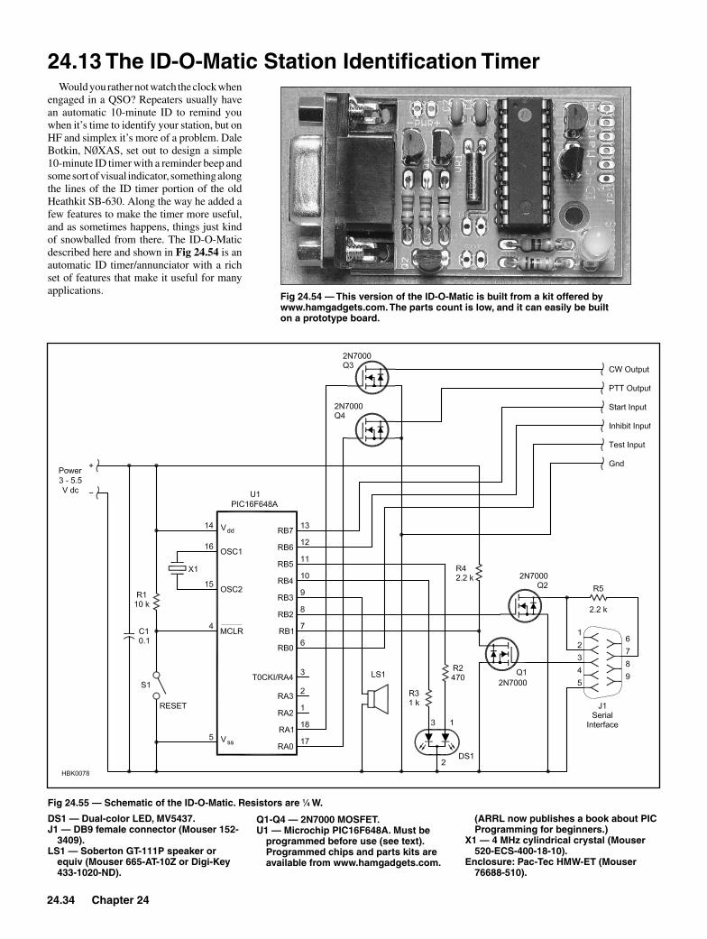
24.34 Chapter 24
Would you rather not watch the clock when engaged in a QSO? Repeaters usually have an automatic 10-minute ID to remind you when it’s time to identify your station, but on HF and simplex it’s more of a problem. Dale Botkin, NØXAS, set out to design a simple 10-minute ID timer with a reminder beep and some sort of visual indicator, something along the lines of the ID timer portion of the old Heathkit SB-630. Along the way he added a few features to make the timer more useful, and as sometimes happens, things just kind of snowballed from there. The ID-O-Matic described here and shown in Fig 24.54 is an automatic ID timer/annunciator with a rich set of features that make it useful for many applications.
Fig 24.54 — This version of the ID-O-Matic is built from a kit offered by www.hamgadgets.com. The parts count is low, and it can easily be built on a prototype board.
Fig 24.55 — Schematic of the ID-O-Matic. Resistors are 1⁄4 W.
DS1 — Dual-color LED, MV5437.J1 — DB9 female connector (Mouser 152-
3409).LS1 — Soberton GT-111P speaker or
equiv (Mouser 665-AT-10Z or Digi-key 433-1020-ND).
Q1-Q4 — 2N7000 MOSFET.U1 — Microchip PIC16F648A. Must be
programmed before use (see text). Programmed chips and parts kits are available from www.hamgadgets.com.
(ARRL now publishes a book about PIC Programming for beginners.)
X1 — 4 MHz cylindrical crystal (Mouser 520-ECS-400-18-10).
Enclosure: Pac-Tec HMW-ET (Mouser 76688-510).
24.13 The ID-O-Matic Station Identification Timer

Station Accessories 24.35
FEATURE HIGHLIGHTSThere’s an old saying that goes, “When all
you have is a hammer, everything looks like a nail.” While the author has a pretty well stocked junk box, he never liked building 555 timers and the like. He tends to use whatever is handy and can cobble together with an ab-solute minimum of parts, and likes to be able to make changes or add features later on. That often means writing firmware for a PIC mi-crocontroller, and this time was no exception.
The basic device uses a single PIC 16F648A processor selected for its memory capacity, internal oscillator, hardware USART and other features. All features are implemented in program code, with just enough external hardware to provide a useful interface to the user. Audio and visual output is used to in-dicate the end of the time period, and one user control is all that is required other than a power switch.
Let’s take a quick look first at the basic features. In its most basic timer mode, a single pushbutton is used to start the timing cycle by resetting the PIC. This starts a 10-minute timer running and lights the green section of a red-green dual color LED. The LED remains green until 60 seconds before the set period expires. With less than 60 seconds remaining, the LED turns yellow; this is accomplished by illuminating both the green and red halves. At 30 seconds the LED begins to blink, alternating between yellow and red. When the time period expires, the LED turns red and the timer starts beeping until you reset it with a pushbutton switch. Now the cycle starts again, ready to remind you in another 10 minutes.
So far so good, but using a PIC like this is a little bit of overkill. Of course no good project is complete until “feature creep” sets in! With the timing and audio portions of the program done, some other features were pretty simple to add. What if you want to ID at some other interval instead of 10 minutes, or have the device automatically ID in Morse code? What if you want to use it for a beacon or a repeater ID device? How about CW and PTT keying outputs for a fox hunt beacon?
Eventually the firmware evolved to have a fairly robust set of features. There is a serial interface for setup using a computer or terminal. You can set the timeout period anywhere from 1 to 32,767 seconds. You can set select a simple beeping alert, or set a Morse ID message with up to 60 characters. For repeater and fox hunt use, there are outputs for PTT and CW keying just in case they might be needed, as well as a couple of inputs intended for COR or squelch inputs if the chip is used in repeater mode. We’ll cover all of that in a bit; first, let’s look at the basic functions and the hardware design.
CIRCUIT DESIGNAs shown in Fig 24.55, the hardware is
quite simple. In its basic form all you need is the PIC, a red and green dual-color LED,
and a few other parts as seen in the schematic. Supply voltage can be 3 to 5.5 V, so you can use three AA alkaline cells. You can also add a 5 V regulator, allowing the use of a 12 V power supply. Despite their size, 9 V batter-ies have surprisingly low capacity and will only last a few days of continuous use in a project like this.
R1 is a pull-up resistor whose value is not critical; 10 kW is a good value. Its function is to hold the !RESET line high until S1 is pressed. R2 and R3 set the current for the red and green sections of the dual LED. They are different values because the red section of the LED is usually substantially brighter than the green. R4 pulls the serial RxD line high when no serial connection is present. For use in the shack to remind you to ID every 10 minutes, that’s all you need.
The original prototype fits in a Pac-Tec enclosure model HMW-ET. For audio out-put, try a tiny Soberton GT-111P speaker. About the size of a small piezo element at 12 mm diameter and about 8 mm tall, this is actually a low current magnetic speaker that can be driven directly from the PIC’s output pinch Switches can be whatever style you like. Many of the parts can be obtained at a local RadioShack, where you may also find a suitable enclosure and battery holder.
A level converter circuit allows you to connect a PC or terminal to set up some of the more advanced features. A single chip solution such as a MAX232 or similar chip could be used, but the circuit shown is effec-tive, very low cost and easy to build. Most modern serial ports do not require full EIA-232 compliance, but will work fine without a negative voltage for the interface lines. Ac-cordingly, the interface presented in the sche-matic simply inverts the polarity of the signals and also converts the ±12 V logic levels that may be present on the PC interface to levels appropriate for the PIC I/O pins. By using MOSFETs instead of the more traditional NPN and PNP transistors we can eliminate some of the parts usually seen in level shifting circuits like this. The only additional compo-nents are Q1, Q2 and R4, a current limiting resistor for the TxD line.
With a terminal or terminal emulator pro-gram you can set your own delay time, CW speed, ID message and select a simple beep or a CW ID. Inputs used for repeater operation (!INHIBIT and !START) are an exercise left to the builder. The thing to remember is that these inputs are active low, and the input voltage must be limited to no more than the PIC’s Vdd supply voltage.
PUTTING THE ID-O-MATIC TO WORkWhen power is applied, the PIC is set
to beep at the end of a 10-minute time-out period. After a series of reminder beeps, it will automatically reset and begin a new timing cycle. To change any of the settings, simply
connect a serial cable to your PC or a dumb terminal and the ID-O-Matic. Any serial com-munication program such as PuTTY, Hyper-Terminal or Minicom can be used. The com-munication settings are 9600 baud, 8 bits, no parity and no handshaking. Hit the ENTER key twice to view and edit the configuration. The program will step through a series of prompts as shown in Fig 24.56. At each prompt you may either enter a new setting or simply hit ENTER to keep the existing setting, shown in parenthesis.
There are a few optional inputs and outputs that could be used to make the timer suitable for use in a “fox” transmitter or repeater.
• Pin 6 (RB0) is the !TEST input. You can momentarily ground this input to hear your ID and/or beacon messages. If no messages have been stored, the ID-O-Matic will announce its firmware version. During normal operation, this pin will select the alternate ID message. This may be useful to indicate, for example, if a repeater site has switched to battery power, or if a “fox” transmitter has been located.
• Pin 12 (RB6) is the !INHIBIT input. This pin is normally held high by the PIC’s inter-nal weak pull-up resistors, and can be driven low by some external signal (squelch, for example) to delay the CW ID until the input goes high.
• Pin 13 (RB7) is the !START input, used only in repeater mode. Also pulled high internally, a LOW logic signal on this pin will start the timer. This can be handy to have your rig or repeater ID 10 minutes after a transmission, but not every 10 minutes. In repeater mode, the chip will ID a few seconds after the first
Fig 24.56 — Using HyperTerminal to set up the ID-O-Matic
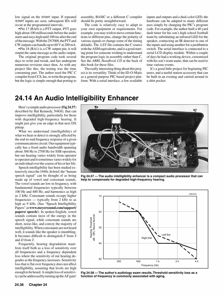
24.36 Chapter 24
low signal on the !START input. If repeated !START inputs are seen, subsequent IDs will occur at the programmed intervals.
• Pin 17 (RA0) is a PTT output. PTT goes high about 100 milliseconds before the audio starts and stays high until 100 ms after the end of the message. With the 2N7000, the PTT and CW outputs can handle up to 60 V at 200 mA.
• Pin 18 (RA1) is a CW output pin; it will output the same message as the audio output.
The original program code took several days to write and tweak, and has undergone numerous revisions since then. As with any project like this, the testing was the time consuming part. The author used the PIC C compiler from CCS, Inc. to write the program, but the logic is simple enough that porting to
assembly, BASIC or a different C compiler should be pretty straightforward.
The code is relatively easy to adapt to your own equipment or requirements. For example, you may wish to move certain func-tions to different pins, change the polarity of various signals or change some of the timing defaults. The .LST file contains the C source with the ASM equivalents, and is a good start-ing point for someone wishing to understand the program logic in assembly rather than C. See the ARRL Handbook CD at the back of this book for these files.
The really interesting thing about this proj-ect is its versatility. Think of the ID-O-Matic as a general purpose PIC based project plat-form. With a serial interface, a few available
inputs and outputs and a dual-color LED, the hardware can be adapted to many different uses simply by changing the PIC’s program code. For example, the author built a 40 yard dash timer for his son’s high school football team by substituting an infrared LED for the speaker, connecting an IR detector to one of the inputs and using another for a pushbutton switch. The serial interface is connected to a serial LCD display module. Within a couple of days he had a working device, customized with his son’s team name, that can be used to time various events.
It’s a good little project for beginning PIC users, and a useful station accessory that can be built in an evening and carried around in a shirt pocket.
24.14 An Audio Intelligibility Enhancer
Fig 24.57 — The audio intelligibility enhancer is a compact audio processor that can help to compensate for degraded high-frequency hearing.
Fig 24.58 — The author’s audiology exam results. Threshold sensitivity loss as a function of frequency is commonly associated with aging.
Here’s a simple audio processor (Fig 24.57) described by Hal Kennedy, N4GG, that can improve intelligibility, particularly for those with degraded high-frequency hearing. It might just give you an edge in that next DX pileup.
What we understand (intelligibility) of what we hear or detect is strongly affected by the end-to-end frequency response of a given communications circuit. Our equipment typi-cally has a fixed audio bandwidth spanning about 300 Hz to 2700 Hz for SSB operation, but our hearing varies widely from operator to operator and it sometimes varies widely for an individual over the course of his or her life.
Speech intelligibility has been studied ex-tensively since the 1940s. In brief, the “human speech signal” can be thought of as being made up of vowel and consonant sounds. The vowel sounds are low in frequency, with fundamental frequencies typically between 100 Hz and 400 Hz, and harmonics as high as 2 kHz. Consonant sounds occupy higher frequencies — typically from 2 kHz to as high as 9 kHz. (See “Speech Intelligibility Papers” at www.meyersound.com/support/papers/ speech/). In spoken English, vowel sounds contain most of the energy in the speech signal, while consonant sounds are short, noise-like, and convey the majority of intelligibility. When consonants are not heard well, it sounds like the speaker is mumbling. It becomes difficult to distinguish F from S and D from T.
Frequently, hearing degradation mani-fests itself both as a loss of sensitivity over all frequencies and a frequency dependent loss where the sensitivity of our hearing de-grades as the frequency increases. Sensitivity loss that is flat over frequency does not affect intelligibility, assuming that levels are high enough to be heard. A simple loss of sensitivi-ty can be addressed by turning up the AF gain!

Station Accessories 24.37
Unfortunately, turning up the gain does not compensate for frequency-dependent loss, and frequency-dependent loss does degrade intelligibility by reducing the ability to hear the consonants in human speech. A quick Web search for “human hearing” will yield a mul-titude of sites describing the basic concepts.
The author’s audiology test results are shown in Fig 24.58. Audiologists refer to this pattern as age induced hearing loss — a roll-off of hearing sensitivity as frequency increases. Fortunately, intelligibility can be improved significantly for those with this common condition, by simply adding am-plification that increases as a function of frequency.
Hearing deficiencies can be much more complex than the typical high frequency loss associated with aging. One’s hearing can in-clude notches and/or peaking as a function of frequency, as well as significant mismatch between the left and right ears. Most of these can be addressed through use of audio cir-cuits whose gain approximates the inverse function of the hearing problem(s). Analog circuit designs become complex when more than a simple high-pass or single-notch filter is required. Modern high-end hearing aids use DSP circuits that break the audio spec-trum into narrow frequency bands, each with programmable gain.
A professional audiology exam and thresh-old sensitivity test results are recommended as the starting point for determining how much, if any, audio shaping might improve your ham radio activities.
A VARIETY OF PRACTICAL OPTIONS
The author’s operating interests require stereo operation to make significant use of a transceiver’s dual receiver function when chasing DX, and to operate two radios simul-taneously in contests. In each case operation is in stereo, with each ear dedicated to one of the two receivers. Monaural designs also have a potential drawback, in that the frequency response adjustments apply equally to both ears. In some cases the frequency response of each ear is different.
Stereo equalizers have been around for de-cades. The most basic are four-band graphic equalizers; they have adjustments to provide up to about 12 dB of gain or attenuation across frequency bands that are centered at four fre-quencies, each frequency typically one octave above the next (an octave is a doubling of frequency). Seven, 10, 12 and 15 band equal-izers are readily available, allowing for finer tailoring of amplification characteristics as the number of bands go up and the frequency range for each band gets smaller.
Parametric equalizers are also available — these differ from graphic equalizers in that the center frequency and bandwidth of
each filter element is adjustable. Prices are very reasonable.
An equalizer is a near-perfect solution to compensating for hearing deficiencies, and the ability to readily adjust gain at multiple frequencies allows optimizing via experimen-tation. Many equalizers are strictly low-level devices and lack sufficient output power to directly drive headphones, requiring an am-plifier if the equalizer is to be inserted between rig and headphones.
Some transceivers include adjustable audio DSP circuits for receive as well as transmit audio. It may be possible to adjust the audio response of your transceiver to improve intel-ligibility without the use of an external device.
CIRCUIT DESCRIPTIONThe heart of this audio intelligibility en-
hancer (AIE) is what audiophiles refer to as a high-pass shelving filter. Shelving filters are sometimes used in high-end audio systems to compensate for deficiencies in crossover networks or loudspeakers. The basic circuit and its frequency response are shown in Fig 24.59. Note that the shape of this response curve is the inverse of the hearing response of Fig 24.58. Referring to Fig 24.59, the cir-cuit provides a gain, AV1, equal to 1.0 for frequencies somewhat below f1 and a higher gain, AV2, that is given by AV2 = 1 + R2/R1 for frequencies somewhat above f2. Fre-quency f1 is given by f1 = 1/[2pC(R1+R2)], and frequency f2 = 1/(2pCR1). Conveniently available component values of R1 = 1.33 kW,
R2 = 6.65 kW, and C = 0.047 µF yield a high frequency gain, AV2 = 6.0, and cut-on and cut-off frequencies of f1 = 425 Hz, and f2 = 2550 Hz. With these values, the circuit gain rises at an average of 3 dB per octave from 300 Hz to 2700 Hz — the frequency range for SSB transmission. For those interested in modifying the design, or using a shelving filter for other purposes, it’s important to note that rearranging the equations yields: f2/f1 = AV2. The ratio of the two break frequencies always equals the maximum gain.
Fig 24.59 also shows a feedback capaci-tor, Cf, which, while not contributing to the shelving filter function, is included as good design practice. The LM324 op amps used to implement the filters have gain-bandwidth products in excess of 1 MHz. Operating them with gain at frequencies above the useful limits of our hearing (and all the way out to beyond 1 MHz) is an open invitation for RFI problems and unwanted high frequency noise. So, feedback capacitor Cf provides high frequency gain roll-off above the frequency f = 1/(2pCfR2) which for the value of Cf in this design (0.0015 µF) is 16.8 kHz.
Fig 24.60 is the complete schematic for the AIE. Two shelving filters, as described above, are used in series in each audio channel. Two filters in series provide sufficient gain change versus frequency to approximately match the author’s high frequency hearing loss, which has a slope of about –7.5 dB/octave across the audiologist’s measuring points from 250 Hz to 4 kHz. Two filters in series provide
Fig 24.59 — Schematic and frequency response for a high-pass audio shelving filter.

24.38 Chapter 24
+6 dB/octave gain change from 300 Hz to 2700 Hz and 31 dB of total gain (AVtotal = AV2 × AV2 = 6 × 6 = 36 or about 31 dB). Some tips for tailoring the circuit to your hearing are included in the next section.
The shelving filters are followed by LM386 audio amplifiers (U2, U3). These provide sufficient output power to drive headphones
or small speakers. LM386s have a built-in voltage gain of 20, so they are preceded by 20:1 voltage dividers (R7+R8, R17+R18) to maintain an end-to-end gain of 1 at low frequencies.
Voltage regulator U4 provides regulated and filtered dc voltage to the shelving filters and the output stages. Current draw for the
AIE is approximately 35 mA from a +13.6 V dc source, if the LED pilot light (D1) is included. D1 draws 10 mA by itself, how- ever, and R21 and D1 can be deleted if current consumption is a concern. Supply voltage is not critical — anything from 12 to 18 V dc will work.
Capacitors C1 and C10 are used to prevent
Fig 24.60 — The audio intelligibility enhancer schematic. Resistors are 1⁄4 W. Parts are available from RadioShack, (www.radioshack.com) and Mouser Electronics (www.mouser.com) as well as many other suppliers. The part numbers shown in parentheses are RadioShack unless otherwise noted.C1, C10 — 0.01 µF, 500 V ceramic (272-
131).C2, C7, C11, C16 — 1.0 µF, 250 V metal
film (272-1055).C3, C5, C12, C14 — 0.0015 µF, 100 V
ceramic (Mouser 80-Ck12BX152k).C4, C6, C9, C13, C15, C18 — 0.047 µF, 50 V,
metal film (272-1068).
C8, C17 — 220 µF, 35 V, electrolytic (272-1029).
C19, C22, C23, C24 — 0.1 µF, 50 V ceramic (272-109).
C20, C21 — 10 µF, 35 V, electrolytic (272-1025).
D1 — LED with holder, green (276-069).S1, S2 — Miniature DPDT (275-626).
U1 — LM324 quad operational amplifier (276-1711).
U2, U3 — LM386 audio amplifier (276-1731).
U4 — LM7805, +5 V regulator (276-1770).Project box, 6×2×1 in (270-1804) (see text).Grid-style PC board, 0.1-in centers
(276-158) (see text).

Station Accessories 24.39
RFI, by bypassing to ground RF that may enter at the inputs. The original AIE without these capacitors suffered interference from loud distorted sounds (unrectified SSB RF) during transmit. C1 and C10 eliminated RFI problems, but they could be insufficient in the presence of large RF fields. If necessary, additional RF filtering can be achieved by adding RF chokes in series with both audio input and output lines.
TAILORING THE DESIGN TO YOUR HEARING
The AIE design presented here is intended to address high frequency hearing loss, and not other hearing deficencies. This AIE de-sign does, however, have a reasonable amount of flexibility for tailoring to an individual’s hearing.
The design as it is presented in Fig 24.60 includes two shelving filters per channel and switch S1. S1 allows selection of one (3 dB/octave amplification) or two (6 dB/octave amplification) filter stages. If you are the only operator of your station and you know your hearing deficiency is less than about 5 dB/octave, the switch and the second filter in each channel can simply be eliminated. If you are unsure of how much high frequency amplification you might need, or in the case where more than one operator may be sharing a station, the switch and the second stages will prove useful. S1 could also be replaced with two switches — one for each channel — if your high frequency hearing is not similar in both ears.
For gain slopes other than 3 dB/octave or 6 dB/octave, one or both filters in either channel can be modified using the equations given earlier. Taking this further, one or both of the op amps in either channel do not have to be shelving filters — they can be used to implement a variety of other filter functions including notching, peaking, or multi-pole functions. Op-amp filter design is covered extensively in circuit design handbooks and on the Internet.
In addition to tailoring the gain change versus frequency, the overall gain of each channel can be adjusted to compensate for the sensitivity differences between ears. Overall gain is adjusted by changing the voltage divid-ers R7+R8 and R17+R18. R8 and R18 can also be replaced with 5-kW potentiometers if adjustable gain is desired.
When considering changing the design, it’s important to know that human speech recogni-tion is remarkably tolerant of deviations from an ideal amplitude versus frequency response curve. Also, personal preference comes into play — you may hear more comfortably with less than complete compensation for high frequency hearing loss. Although 6 dB/octave compensation closely matches the author’s hearing loss, he usually has the AIE switched
to 3 dB/octave compensation. At this setting, intelligibility is improved considerably.
CONSTRUCTIONWith a few exceptions, the layout of the
component parts is not critical. The leads on the IC power decoupling capacitors (C22, C23, C24) and all leads to the op amp inputs should be kept as short as possible. Be sure to make the U1 power connections at pins 4 and 11.
The completed AIE is shown in Figs 24.61 and 24.62. The prototype is built on a grid style PC board with 0.1 inch centers — these are available from RadioShack — cut to fit snugly in a 6×2×1 inch plastic project box. Parts numbers for the PC board and the proj-ect box are included in the parts list. A PC board is available from FAR Circuits (www.farcircuits.net).
Two cautions are in order. First, building an AIE as small as the prototype requires small
tools, a large magnifying glass and patience. Since the circuit design is not particularly sensitive to layout, consider using a larger layout and a larger enclosure. The second caution is with regard to using a plastic en-closure. Susceptibility to RFI and 60 Hz hum pickup will be greatly reduced by using a metal enclosure. If you have lots of RF in your shack you may have no choice but to use a metal enclosure.
Several of the components are not avail-able from RadioShack, but they are readily available from mail order suppliers and can be found in a well-stocked junk box. Several sub-stitutions can be made to yield an “all Radio Shack” design. The 1.33-kW resistors can be made from a 1-kW and a 330 W resistor in series; the 6.65-kW resistors can be made from two 3.3-kW resistors in series and the 1.5-kW re-sistor can be made from a 1-kW and a 470 W resistor in series. The value of the 0.0015 µF feedback capacitors is not critical (C3, C5,
Fig 24.61 — A close-up of the AIE before mounting in the project box. It all fits neatly within a 6×2×1 inch enclosure if you have the patience to build within tight spaces.
Fig 24.62 — The AIE takes up little desk space. It plugs inline between the transceiver and headphones and requires 13.6 V dc. In the author’s shack, the unit is powered from a transceiver accessory jack and is always switched on.

24.40 Chapter 24
C12, C14) — 0.001 µF disk ceramics can be substituted (RadioShack 272-126).
HOW WELL DOES IT WORk?Intelligibility is absolutely crucial to main-
taining high QSO rates and correct logging in contests, and in pulling the weak ones out of the noise when DXing or operating in less-than-ideal conditions. The AIE has provided the author with an immense improvement in both activities. It’s just as helpful for reduc-ing listening fatigue during ragchewing or general listening as well.
A real surprise was how much intelligibil-ity improved on CW. This may seem coun-terintuitive at first, if you view “continuous wave” as comprising a single frequency. From a communications standpoint, however, the CW waveform is not continuous — it is com-prised of elements — dots and dashes. The leading and trailing edges of each element are made up of frequencies higher than the carrier frequency, and hearing these helps
the listener separate one element from the next. When the rise and/or fall times of the elements are very fast compared to the carrier frequency, the high frequency content of the waveform becomes sufficiently large to cause key clicks. Very slow rise and/or fall times produce the opposite of clicks — a sound that experienced CW operators describe as “mushy.” Mushy code is very difficult to copy, particularly at high speeds, because the abil-ity to decipher when an element has started or stopped has been reduced. Degraded high frequency hearing has the same detrimental effect on CW intelligibility as slowing down the waveform edges — it makes a properly formed CW waveform sound mushy. The AIE restores perception of the waveform edges in CW, just as it does for speech.
How much an AIE or any other approach to compensating for your hearing deficiencies will help you depends, to a large degree, on the state of your hearing. The more you have lost, the more you have to gain back. Audio
shaping may also offer some intelligibility improvement if your hearing is within normal limits. Typical receiver bandwidths are nar-rower than the audio range needed to fully support intelligibility — some of this can be gained back with high frequency amplifica-tion.
One cautionary note from Jim Collins, N9FAY, a designer in the hearing aid industry. At low volume levels, a device such as the AIE is helpful in improving intelligibility. At high volume levels, the audio will start to sound “tinny.” This happens because as sound levels increase, the corrective frequency curve must flatten. At upper sound levels of comfortable hearing, it becomes almost a flat line with unity gain, In other words, the hearing re-sponse is close to normal at high sound levels. If a device like the AIE is used for prolonged periods at high volume levels, it may ac- celerate hearing loss at upper frequencies. For more discussion, see Technical Correspondence in May 2005 QST, p 70.
24.15 An Audio Interface Unit for Field Day and Contesting
For Field Day and multioperator contest operation, it’s sometimes desirable for a log-ger or observer to listen to a transceiver in addition to the main operator. The project shown in Fig 24.63, by John Raydo, KØIZ, makes two-person operation more efficient. Dual stereo headphone jacks, volume controls and an external speaker jack are provided, as well as jacks for both dynamic and electret microphones and an intercom feature for op-erator and logger to more easily communicate via headset mics.
There are times when the operator and log-ger need to talk to each other, for example to resolve a call-sign ambiguity. With this unit the operator can initiate two-way inter-com communication by closing an intercom switch. The logger, however, can only initiate one-way intercom to the operator. This is so that the logger can’t inadvertently cut off the operator during a contact. To respond, the operator closes his intercom switch. In both instances, radio volume is reduced for “talk-over” during intercom use.
Both the operator and logger need headsets with microphones. The unit has two intercom switches plus jacks for optional foot switches for hands-free operation. Here’s how it works:
Operator communicating with the logger: The operator presses and holds the OPERATOR
TALK switch (S3 on the unit or by using a foot switch connected to J4). This disconnects the operator mic from radio. Both mics are con-
Fig 24.63 — Front view of the audio interface box. Operator controls are on the left and logger controls are on the right.
nected via an internal amplifier to both head-phones. Radio volume is reduced (adjustable using the RADIO VOL control). Operator and logger can talk to each other.
Logger communicating with the operator: The logger presses and holds the LOGGER TALK switch (S4 on the unit or by using a foot switch connected to J5). Logger mic is connected via an internal amplifier to both headphones. Operator mic remains connected to radio and can still transmit on the radio. Radio volume is reduced. The operator can respond to the logger by pressing the OPERATOR TALK switch.
CIRCUIT DESCRIPTIONThe circuit diagram shown in Fig 24.64 is
designed for use with dynamic microphones such as the HC4 and HC5 elements used in various Heil headsets, or for Heil iC type headsets that use an electret element. The electret mic jacks supply the required dc for that type microphone. Mic bias current is limited to less than 1 mA to avoid damage if a dynamic mic is accidentally plugged into the wrong jack. The higher electret output is reduced by resistors R11 and R28.
Both mics have preamplifiers with 34 dB gain set by the ratio of the resistors R4/R3 and R9/R8. The INTERCOM volume controls, R14 and R15, allow operator and logger to indi-vidually adjust their intercom volumes. The preamps feed a single 2-W intercom amplifier.
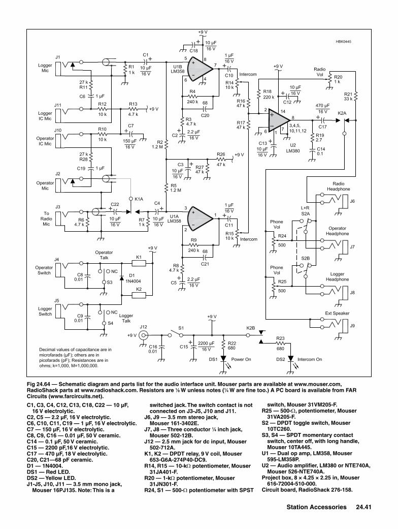
Station Accessories 24.41
Fig 24.64 — Schematic diagram and parts list for the audio interface unit. Mouser parts are available at www.mouser.com, RadioShack parts at www.radioshack.com. Resistors are 1⁄8 W unless notes (1⁄4 W are fine too.) A PC board is available from FAR Circuits (www.farcircuits.net).
C1, C3, C4, C12, C13, C18, C22 — 10 µF, 16 V electrolytic.
C2, C5 — 2.2 µF, 16 V electrolytic.C6, C10, C11, C19 — 1 µF, 16 V electrolytic.C7 — 150 µF, 16 V electrolytic.C8, C9, C16 — 0.01 µF, 50 V ceramic.C14 — 0.1 µF, 50 V ceramic.C15 — 2200 pF,16 V electrolytic.C17 — 470 µF, 18 V electrolytic.C20, C21—68 pF ceramic.D1 — 1N4004.DS1 — Red LED.DS2 — Yellow LED.J1-J5, J10, J11 — 3.5 mm mono jack,
Mouser 16PJ135. Note: This is a
switched jack. The switch contact is not connected on J3-J5, J10 and J11.
J6, J9 — 3.5 mm stereo jack, Mouser 161-3402E.
J7, J8 — Three conductor 1⁄4 inch jack, Mouser 502-12B.
J12 — 2.5 mm jack for dc input, Mouser 502-712A.
k1, k2 — DPDT relay, 9 V coil, Mouser 653-G6A-274P40-DC9.
R14, R15 — 10-kW potentiometer, Mouser 31JA401-F.
R20 — 1-kW potentiometer, Mouser 31JN301-F.
R24, S1 — 500-W potentiometer with SPST
switch, Mouser 31VM205-F.R25 — 500-W, potentiometer, Mouser
31VA205-F.S2 — DPDT toggle switch, Mouser
10TC260.S3, S4 — SPDT momentary contact
switch, center off, with long handle, Mouser 10TA445.
U1 — Dual op amp, LM358, Mouser 595-LM358P.
U2 — Audio amplifier, LM380 or NTE740A, Mouser 526-NTE740A.
Project box, 8 × 4.25 × 2.25 in, Mouser 616-72004-510-000.
Circuit board, RadioShack 276-158.

24.42 Chapter 24
Closing the OPERATOR TALK switch trans-fers the operator mic from radio to intercom preamp and amplifier via K1 and then to the headphones via K2. Pressing the LOGGER TALK switch will also activate K2 (but not K1). Dur-ing intercom use, audio from the radio passes through control R20 (RADIO VOL) at reduced volume. S2 (L+R) allows selection of both left and right sides of the headphones or only the right side, for the intercom. The operator and logger each have individual headphone PHONE VOL controls R24 and R25 (the op-erator control also incorporates the POWER switch, S1).
CONSTRUCTIONThe unit shown is built in a PacTec plastic
box. The front panel has the control switches and volume controls described in the previ-ous section. The back panel (Fig 24.65) has1⁄4-inch stereo jacks for two pair of head-phones, two 3.5-mm mono jacks for head-set microphones, 3.5-mm stereo and mono jacks for connection to the radio’s headphone and mic jacks, one stereo 3.5-mm jack for a speaker, two 3.5-mm mono jacks for foot switches and a jack for a 9-V power supply (a wall wart is okay). A 12-V dc supply can be substituted if K1 and K2 are changed to 12-V units and the LED series resistors R22 and R23 are changed to 1 kW.
Other than controls and jacks, most com-ponents are mounted on a RadioShack pro-totype circuit board supported by four 1⁄2 inch spacers and shown in the box in Fig 24.66. A suggested parts layout is shown in Fig 24.67. Point-to-point wiring is used between circuit board pads and is not particularly critical. A PC board for this project has been developed
by FAR Circuits (www.farcircuits.net).Connections to both mic jacks and the radio
mic jack use shielded cable to reduce hum and risk of interference pickup. Connect the shields on the operator and radio mic cables to a common ground point on the circuit board near U1. Bypass capacitors C8, C9 and C16 and resistor R6 are mounted at their respective jacks. Rub-on lettering, followed by a couple light coats of clear plastic spray, helps give a professional appearance.
Connecting an external speaker in addi-
Fig 24.67 — Suggested parts layout for audio interface box.
Fig 24.65 — Rear view of the audio interface box. Operator jacks are on the right, logger on the left. Connections to the radio are in the center.
Fig 24.66 — Inside view of the audio interface box. A RadioShack project board is used for most components.
C15
C17
K1
K2
U2 LM380
U1 LM358
C7
C19
C21
C20
C1
C5
C11
C2
C3
C12
C10
C14 R
1
R17
R16
D1+
R26
R27
R4
R23
R19
R21
R9
C4
R6
R12 R7
R2
R13
C13
R3
C18
R18
R5 R8
QS0806-Raydo05
tion to two headphones might be too much of a load for some radios and cause reduced volume and/or distortion. Try an inexpensive amplified computer speaker plugged into the audio interface external speaker jack to reduce the load.
You will need two cables to connect the unit to your radio. A 3.5 mm mono plug-to-plug shielded cable for the mic circuit is compat-ible with a Heil headset mic. A 3.5 mm stereo plug-to-plug cable (RadioShack 42-2387 plus 274-367 adapter) works for the earphones.