contemporary logic design sequential logic © r.h. katz transparency no. 12-1 chapter #6: sequential...
Post on 22-Dec-2015
230 views
TRANSCRIPT
Contemporary Logic DesignSequential Logic
© R.H. Katz Transparency No. 12-1
Chapter #6: Sequential Logic Design
6.1 -- Sequential Switching Networks
Contemporary Logic DesignSequential Logic
© R.H. Katz Transparency No. 12-2
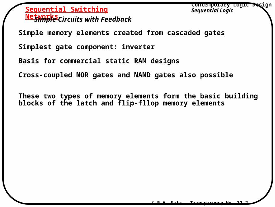
Sequential Switching NetworksSimple Circuits with Feedback
Simple memory elements created from cascaded gates
Simplest gate component: inverter
Basis for commercial static RAM designs
Cross-coupled NOR gates and NAND gates also possible
These two types of memory elements form the basic building blocks of the latch and flip-fllop memory elements
Contemporary Logic DesignSequential Logic
© R.H. Katz Transparency No. 12-3
Sequential Switching NetworksSimple Circuits with Feedback
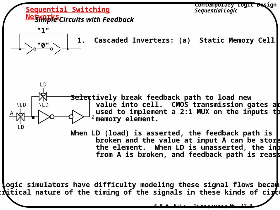
1. Cascaded Inverters: (a) Static Memory Cell"0"
"1"
Selectively break feedback path to load new value into cell. CMOS transmission gates are used to implement a 2:1 MUX on the inputs to the memory element.
When LD (load) is asserted, the feedback path is broken and the value at input A can be stored in the element. When LD is unasserted, the input from A is broken, and feedback path is reasserted.
Z
LD
\LD
LD
\LD
A
Many logic simulators have difficulty modeling these signal flows because ofthe critical nature of the timing of the signals in these kinds of circuits.
Contemporary Logic DesignSequential Logic
© R.H. Katz Transparency No. 12-4
Sequential Switching NetworksInverter Chains -- (b) Ring Oscillators
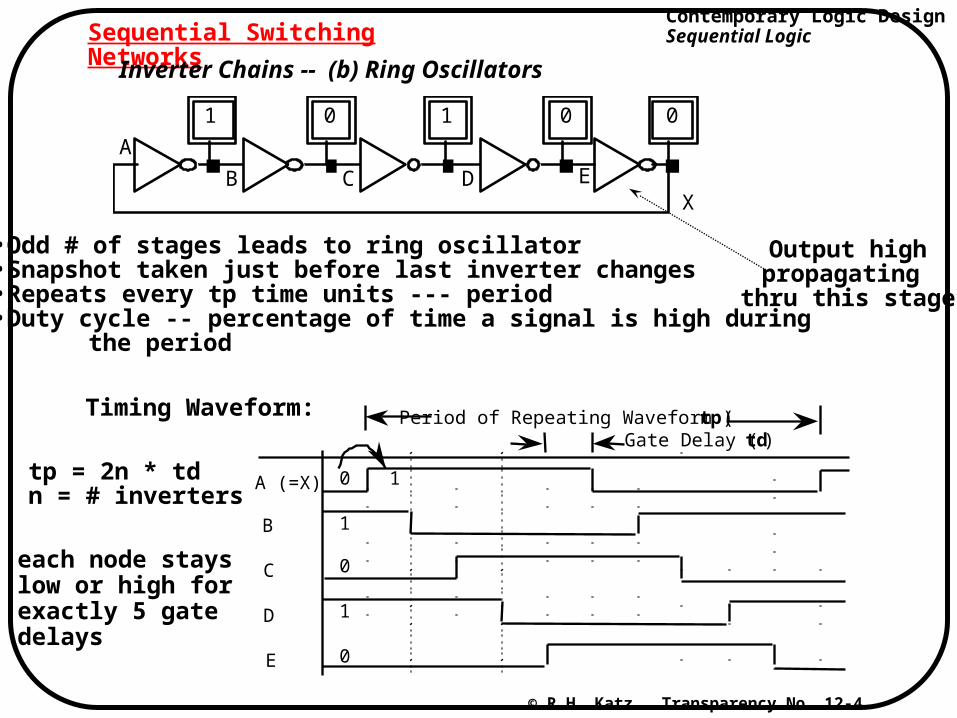
•Odd # of stages leads to ring oscillator•Snapshot taken just before last inverter changes•Repeats every tp time units --- period•Duty cycle -- percentage of time a signal is high during
the period
Output highpropagating
thru this stage
Timing Waveform:
A (=X) B C D E
Period of Repeating Waveform ( tp )Gate Delay ( td)
0
1
0
1
0
1tp = 2n * tdn = # inverters
A
B C D E
1 0 0 0 1
X
each node stayslow or high forexactly 5 gatedelays
Contemporary Logic DesignSequential Logic
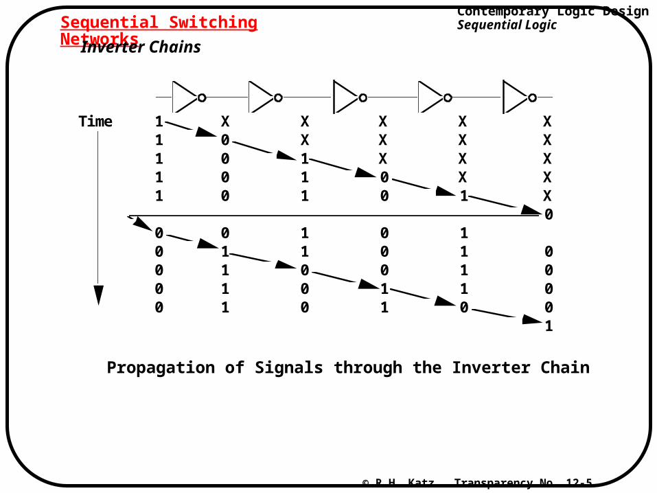
© R.H. Katz Transparency No. 12-5
Sequential Switching NetworksInverter Chains
1 1 1 1 1
0 0 0 0 0
X0 0 0 0
0 1 1 1 1
XX1 1 1
1 1 0 0 0
X X X 0 0 0 0 0 1 1
X X X X 1 1 1 1 1 0
X X X X X 0 0 0 0 0 1
Time
Propagation of Signals through the Inverter Chain
Contemporary Logic DesignSequential Logic
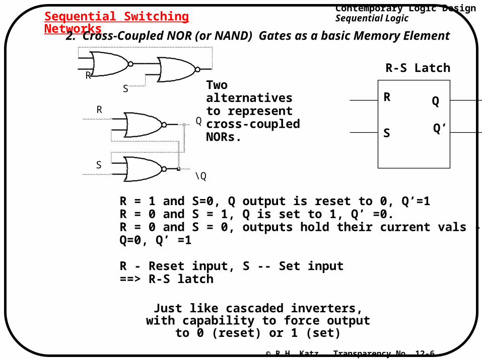
© R.H. Katz Transparency No. 12-6
Sequential Switching Networks
2. Cross-Coupled NOR (or NAND) Gates as a basic Memory Element
R
R
S
S
Q
\Q
R = 1 and S=0, Q output is reset to 0, Q’=1R = 0 and S = 1, Q is set to 1, Q’ =0.R = 0 and S = 0, outputs hold their current vals --Q=0, Q’ =1
R - Reset input, S -- Set input==> R-S latch
Just like cascaded inverters,with capability to force output
to 0 (reset) or 1 (set)
Two alternatives to representcross-coupled NORs.
R-S Latch
R
S
Q
Q’
Contemporary Logic DesignSequential Logic
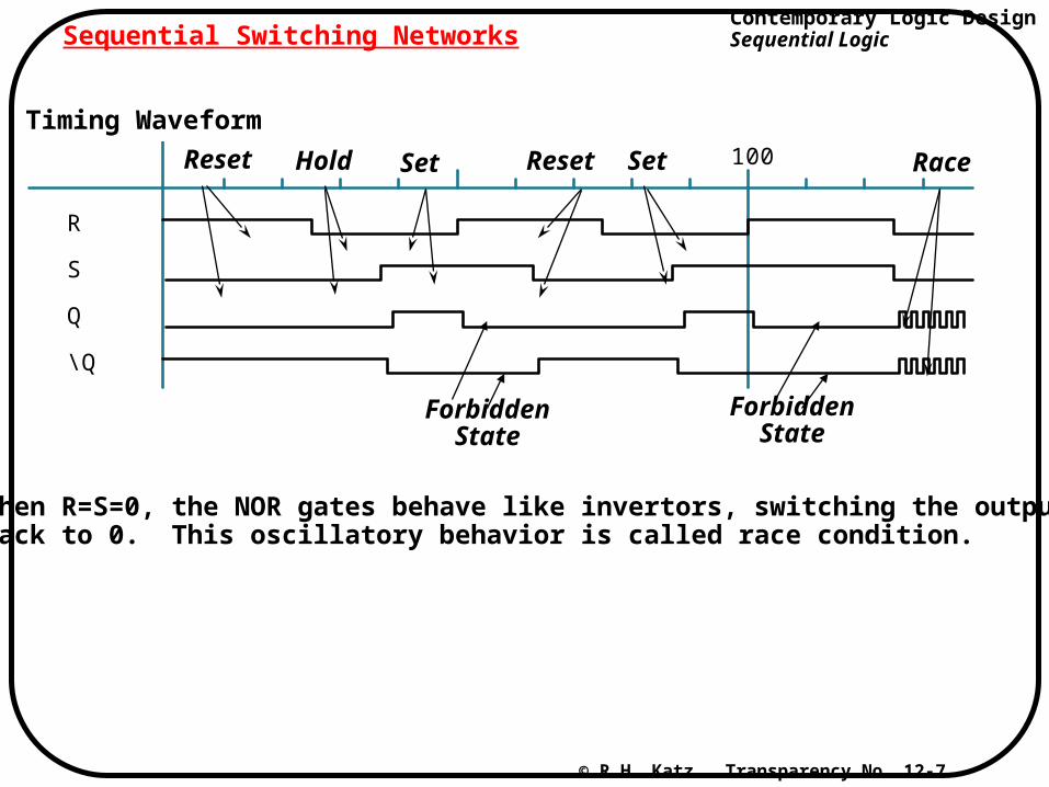
© R.H. Katz Transparency No. 12-7
Sequential Switching Networks
100
R
S
Q
\ Q
Timing Waveform
Reset Hold Set
ForbiddenState
Reset Set
ForbiddenState
Race
When R=S=0, the NOR gates behave like invertors, switching the outputsback to 0. This oscillatory behavior is called race condition.

Contemporary Logic DesignSequential Logic
© R.H. Katz Transparency No. 12-8
Sequential Switching NetworksState Behavior of R-S Latch
Truth Table Summary of R-S Latch Behavior
Q
hold 0 1
unstable
S
0 0 1 1
R
0 1 0 1
-- reset
-- set
Contemporary Logic DesignSequential Logic
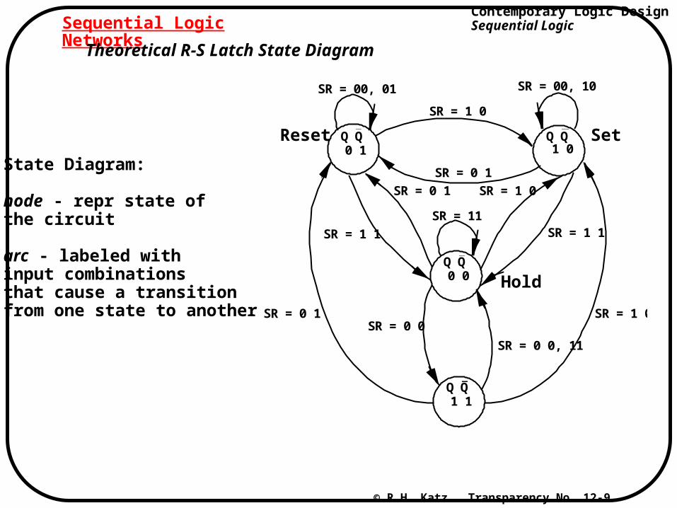
© R.H. Katz Transparency No. 12-9
Sequential Logic Networks
Theoretical R-S Latch State Diagram
Q Q Q Q
Q Q
0 1 1 0
0 0
SR = 1 0
SR = 0 1
SR = 0 1
SR = 1 1
SR = 1 0
SR = 1 1
SR = 00, 01 SR = 00, 10
Q Q1 1
SR = 0 0
SR = 0 0, 11
SR = 11
SR = 1 0SR = 0 1
State Diagram:
node - repr state ofthe circuit
arc - labeled withinput combinationsthat cause a transitionfrom one state to another
Reset Set
Hold
Contemporary Logic DesignSequential Logic
© R.H. Katz Transparency No. 12-10
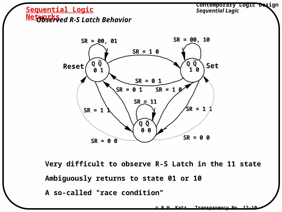
Sequential Logic NetworksObserved R-S Latch Behavior
Q Q Q Q
Q Q
0 1 1 0
0 0
SR = 1 0
SR = 0 1
SR = 0 1
SR = 1 1
SR = 1 0
SR = 1 1
SR = 00, 01 SR = 00, 10
SR = 0 0
SR = 11
SR = 0 0
Very difficult to observe R-S Latch in the 11 state
Ambiguously returns to state 01 or 10
A so-called "race condition"
Reset Set
Contemporary Logic DesignSequential Logic
© R.H. Katz Transparency No. 12-11
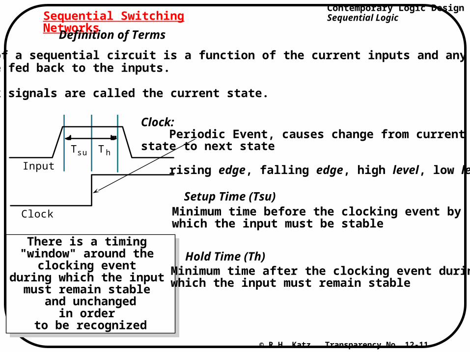
Input
Clock
T su T h
Sequential Switching Networks
Definition of Terms
Setup Time (Tsu)
Clock: Periodic Event, causes change from current state to next state
rising edge, falling edge, high level, low level
There is a timing "window" around the
clocking event during which the input
must remain stable and unchanged
in order to be recognized
There is a timing "window" around the
clocking event during which the input
must remain stable and unchanged
in order to be recognized
Minimum time before the clocking event by which the input must be stable
Hold Time (Th)Minimum time after the clocking event during which the input must remain stable
Output of a sequential circuit is a function of the current inputs and any signalsthat are fed back to the inputs.
Feedback signals are called the current state.
Contemporary Logic DesignSequential Logic
© R.H. Katz Transparency No. 12-12
Sequential Switching Networks
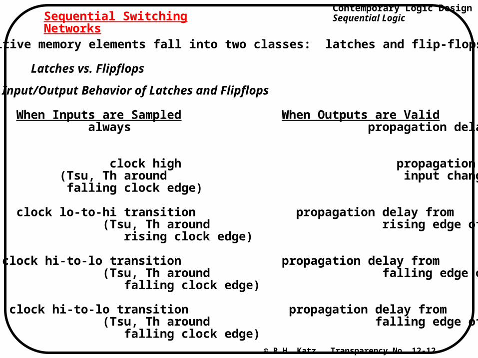
Latches vs. Flipflops
Input/Output Behavior of Latches and Flipflops
Type When Inputs are Sampled When Outputs are Validunclocked always propagation delay from latch input change
level clock high propagation delay fromsensitive (Tsu, Th around input changelatch falling clock edge)
positive edge clock lo-to-hi transition propagation delay fromflipflop (Tsu, Th around rising edge of clock rising clock edge)
negative edge clock hi-to-lo transition propagation delay fromflipflop (Tsu, Th around falling edge of clock falling clock edge)
master/slave clock hi-to-lo transition propagation delay fromflipflop (Tsu, Th around falling edge of clock falling clock edge)
Primitive memory elements fall into two classes: latches and flip-flops
Contemporary Logic DesignSequential Logic
© R.H. Katz Transparency No. 12-13
Sequential Switching Networks
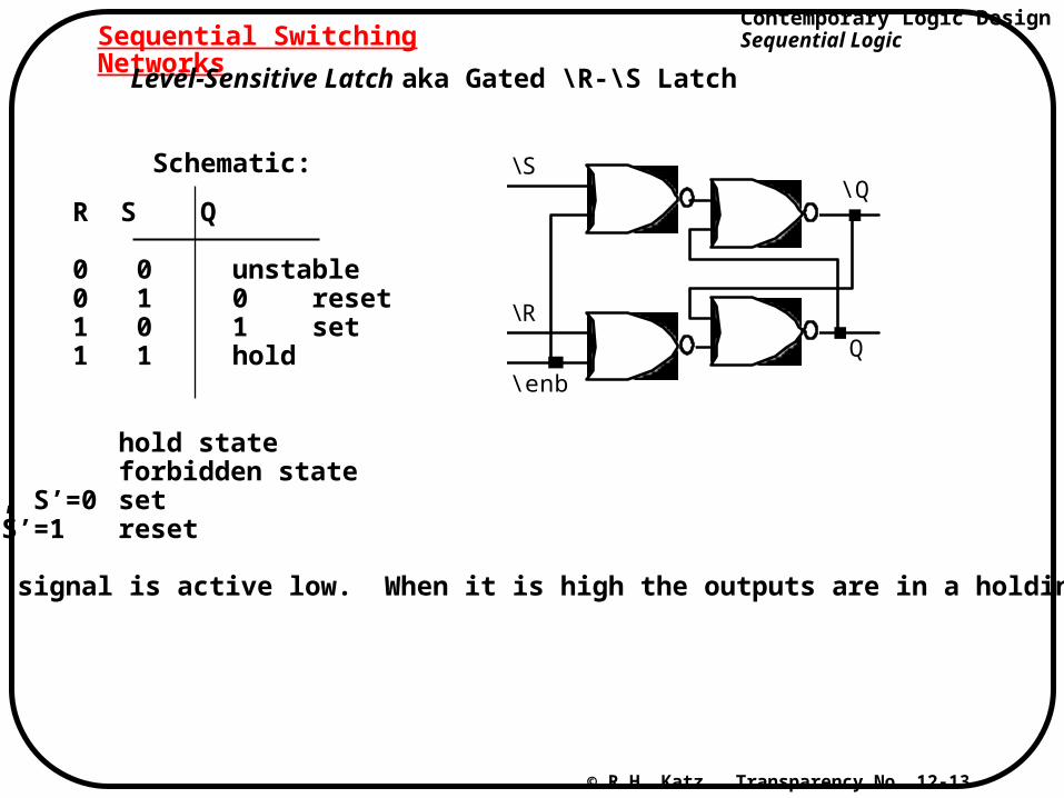
Level-Sensitive Latch
\ S
\ R
\ Q
Q
\enb
Schematic:
aka Gated \R-\S Latch
R=S=1 hold stateR=S=0 forbidden stateR’ = 1, S’=0 setR’=0, S’=1 reset
Enable signal is active low. When it is high the outputs are in a holding state.
R S Q
0 0 unstable0 1 0 reset1 0 1 set1 1 hold
Contemporary Logic DesignSequential Logic
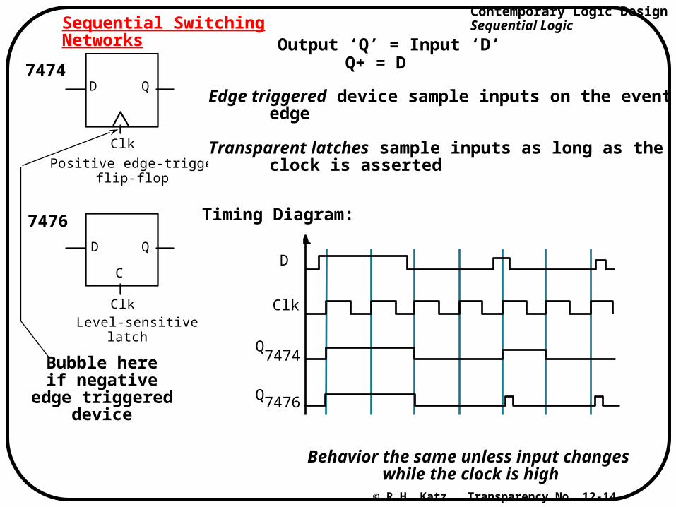
© R.H. Katz Transparency No. 12-14
Sequential Switching Networks
7474
7476
Bubble hereif negative
edge triggereddevice
Timing Diagram:
Behavior the same unless input changes while the clock is high
Edge triggered device sample inputs on the event edge
Transparent latches sample inputs as long as the clock is assertedPositive edge-triggered
flip-flop
Level-sensitive latch
D Q
D Q
C
Clk
Clk
D
Clk
Q
Q
7474
7476
Output ‘Q’ = Input ‘D’Q+ = D
Contemporary Logic DesignSequential Logic
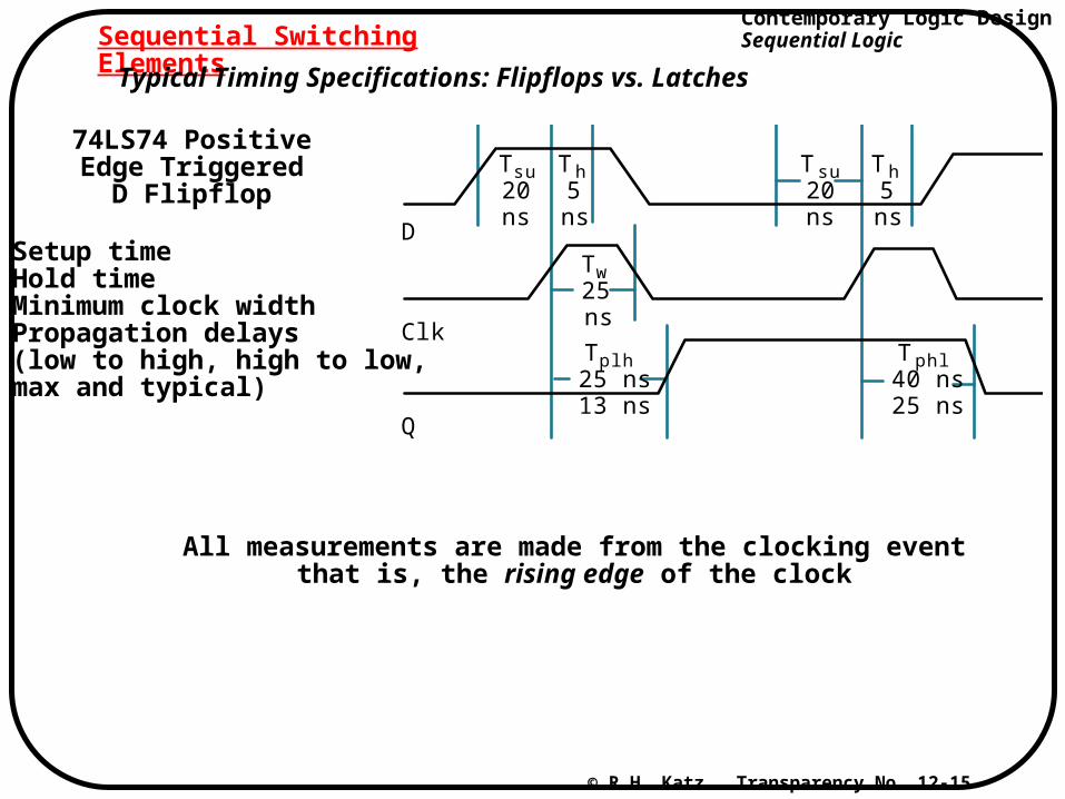
© R.H. Katz Transparency No. 12-15
Sequential Switching ElementsTypical Timing Specifications: Flipflops vs. Latches
74LS74 PositiveEdge Triggered
D Flipflop
• Setup time• Hold time• Minimum clock width• Propagation delays (low to high, high to low, max and typical)
All measurements are made from the clocking eventthat is, the rising edge of the clock
D
Clk
Q
T su 20 ns
T h 5 ns
T w 25 ns
T plh 25 ns 13 ns
T su 20 ns
T h 5 ns
T phl 40 ns 25 ns
Contemporary Logic DesignSequential Logic
© R.H. Katz Transparency No. 12-16
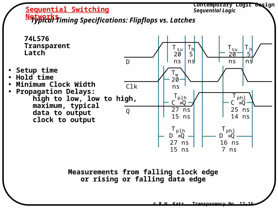
Sequential Switching NetworksTypical Timing Specifications: Flipflops vs. Latches
74LS76TransparentLatch
• Setup time• Hold time• Minimum Clock Width• Propagation Delays: high to low, low to high, maximum, typical data to output clock to output
Measurements from falling clock edgeor rising or falling data edge
T su 20 ns
T h 5 ns
T su 20 ns
T h 5 ns
T w 20 ns
T plh C » Q 27 ns 15 ns
T phl C » Q 25 ns 14 ns
T plh D » Q 27 ns 15 ns
T phl D » Q 16 ns 7 ns
D
Clk
Q
Contemporary Logic DesignSequential Logic
© R.H. Katz Transparency No. 12-17
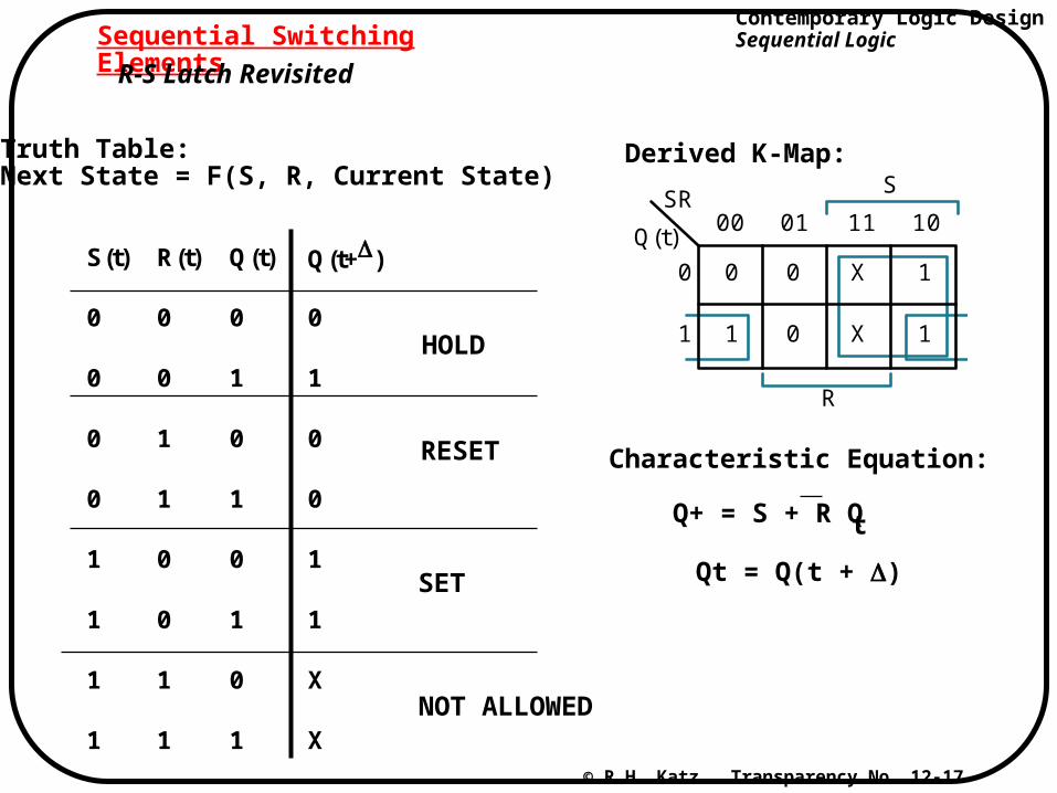
S(t) R(t) Q(t) Q(t+)
0 0 0 0
0 0 1 1
0 1 0 0
0 1 1 0
1 0 0 1
1 0 1 1
1 1 0 X
1 1 1 X
1
Sequential Switching ElementsR-S Latch Revisited
Truth Table:Next State = F(S, R, Current State)
Derived K-Map:
Characteristic Equation:
Q+ = S + R Q t
R
SR 00 01 11 10
0 0 X 1
1 0 X 1
0
1
Q ( t )
S
Qt = Q(t + )
HOLD
RESET
SET
NOT ALLOWED
Contemporary Logic DesignSequential Logic
© R.H. Katz Transparency No. 12-18
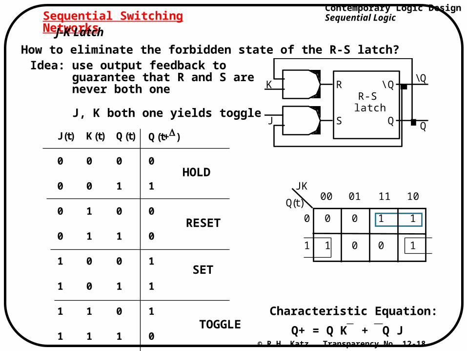
Sequential Switching NetworksJ-K Latch
How to eliminate the forbidden state of the R-S latch?Idea: use output feedback to guarantee that R and S are never both one
J, K both one yields toggle
Characteristic Equation:
Q+ = Q K + Q J
R-S latch
K
J S
R
Q
\ Q \ Q
Q J(t) K(t) Q(t) Q(t+)
0 0 0 0
0 0 1 1
0 1 0 0
0 1 1 0
1 0 0 1
1 0 1 1
1 1 0 1
1 1 1 0
HOLD
RESET
SET
TOGGLE
JK 00 01 11 10
0 0 1 1
1 0 0 1
0
1
Q ( t )
Contemporary Logic DesignSequential Logic
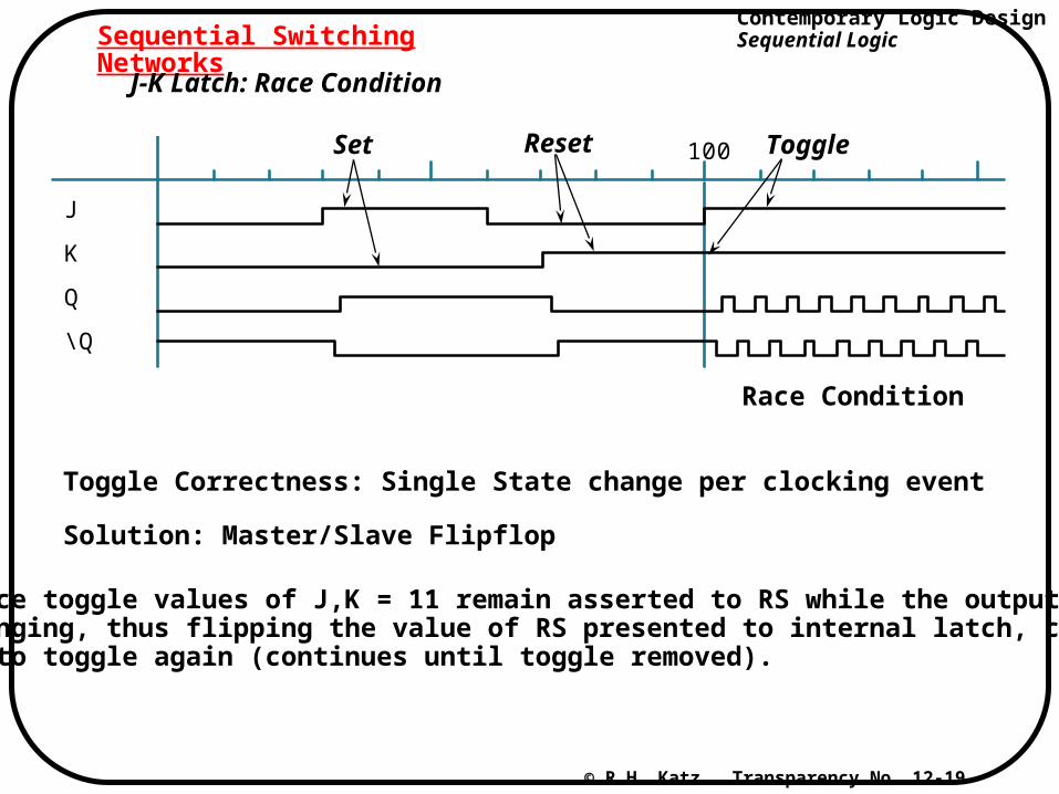
© R.H. Katz Transparency No. 12-19
J
K
Q
\ Q
100
Sequential Switching Networks
J-K Latch: Race Condition
Set Reset Toggle
Race Condition
Toggle Correctness: Single State change per clocking event
Solution: Master/Slave Flipflop
Since toggle values of J,K = 11 remain asserted to RS while the output ischanging, thus flipping the value of RS presented to internal latch, causingit to toggle again (continues until toggle removed).
Contemporary Logic DesignSequential Logic
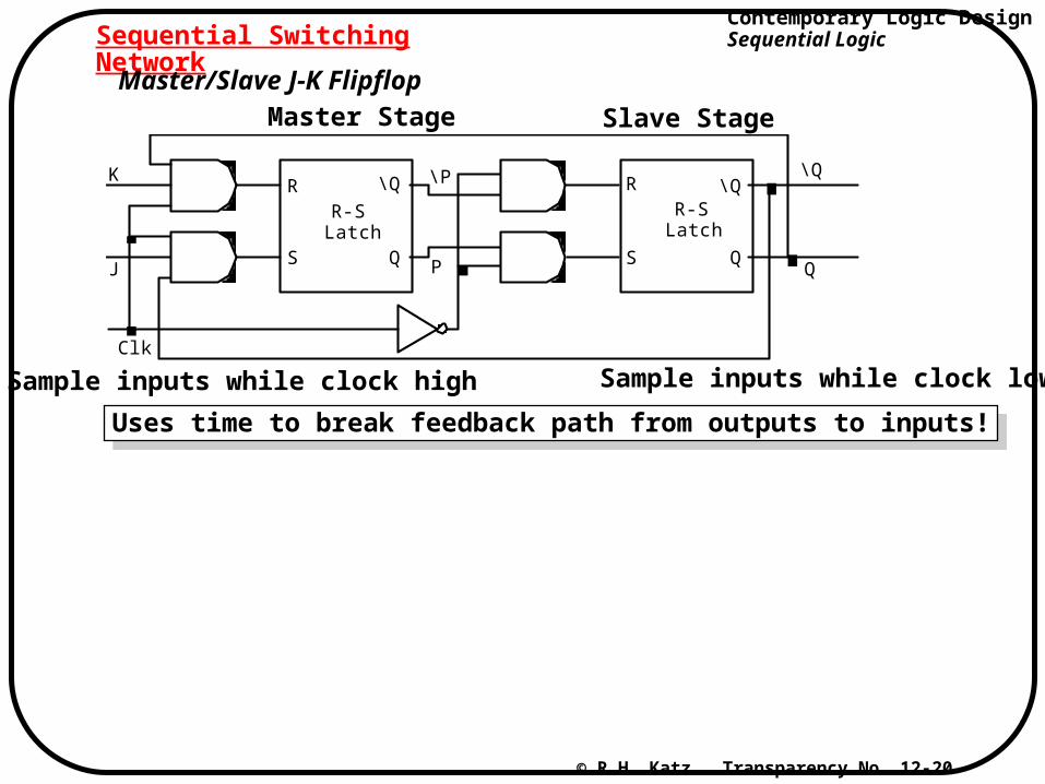
© R.H. Katz Transparency No. 12-20
Sequential Switching Network
Master/Slave J-K FlipflopMaster Stage Slave Stage
Sample inputs while clock high Sample inputs while clock low
Uses time to break feedback path from outputs to inputs!Uses time to break feedback path from outputs to inputs!
J
R-S Latch
R-S Latch
K R
S
Clk
\Q
Q
\P
P
R
S
\Q
Q
\Q
Q
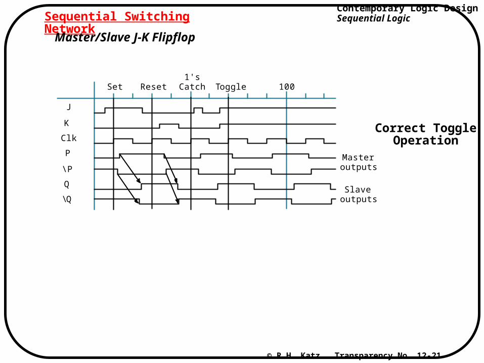
Contemporary Logic DesignSequential Logic
© R.H. Katz Transparency No. 12-21
Sequential Switching Network
Master/Slave J-K Flipflop
Correct ToggleOperation
Master outputs
Slave outputs
Set Reset T oggle 1's
Catch 100
J
K
Clk
P
\ P
Q
\ Q
Contemporary Logic DesignSequential Logic
© R.H. Katz Transparency No. 12-22
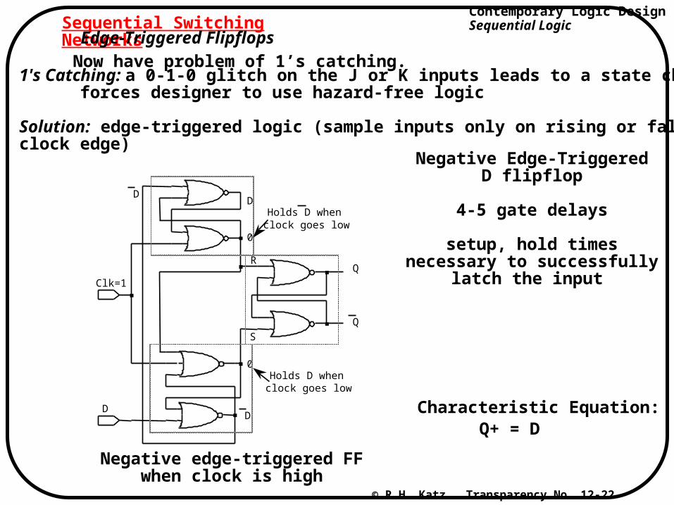
Sequential Switching NetworksEdge-Triggered Flipflops
1's Catching: a 0-1-0 glitch on the J or K inputs leads to a state change! forces designer to use hazard-free logic
Solution: edge-triggered logic (sample inputs only on rising or fallingclock edge)
Negative Edge-TriggeredD flipflop
4-5 gate delays
setup, hold timesnecessary to successfully
latch the input
Characteristic Equation:Q+ = D
Q
Q
D
Clk=1
R
S
0
0
D
DD
Holds D when clock goes low
Holds D when clock goes low
Negative edge-triggered FFwhen clock is high
Now have problem of 1’s catching.
Contemporary Logic DesignSequential Logic
© R.H. Katz Transparency No. 12-23
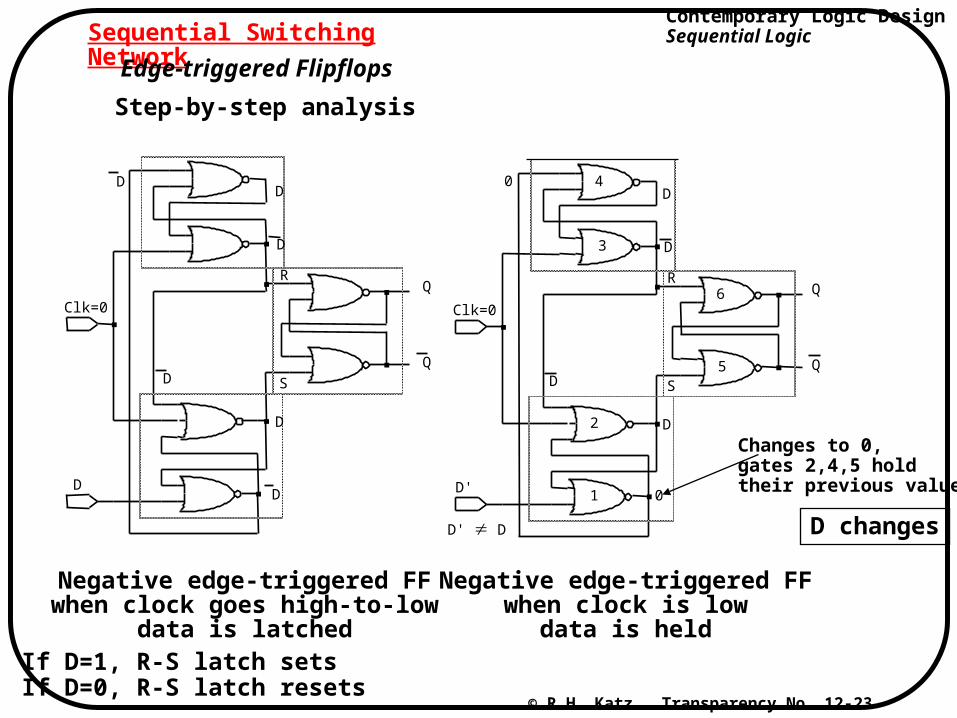
Sequential Switching NetworkEdge-triggered Flipflops
Step-by-step analysis
Q
Q
D
Clk=0
R
S
D
DD
D
D
D
Negative edge-triggered FFwhen clock goes high-to-low
data is latched
Negative edge-triggered FFwhen clock is low
data is held
Q
Q
D'
Clk=0
R
S
D
D
D
D
D' D
0
0
1
2
3
4
5
6
If D=1, R-S latch setsIf D=0, R-S latch resets
Changes to 0,gates 2,4,5 holdtheir previous values
D changes
Contemporary Logic DesignSequential Logic
© R.H. Katz Transparency No. 12-24
Sequential Switching Networks
Positive vs. Negative Edge Triggered Devices
Positive Edge Triggered
Inputs sampled on rising edgeOutputs change after rising edge
Negative Edge Triggered
Inputs sampled on falling edgeOutputs change after falling edge
Positive edge- t riggered FF
Negative edge- t riggered FF
D
Clk
Q pos
\ Q pos
Q neg
\ Q neg
100
Contemporary Logic DesignSequential Logic
© R.H. Katz Transparency No. 12-25
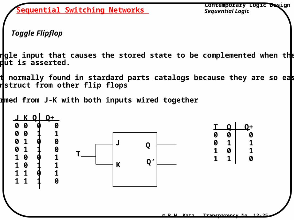
Toggle Flipflop
Single input that causes the stored state to be complemented when the input is asserted.
Not normally found in stardard parts catalogs because they are so easy toconstruct from other flip flops
Formed from J-K with both inputs wired together
Sequential Switching Networks
J
K
Q
Q’T
J K Q Q+0 0 0 00 0 1 10 1 0 00 1 1 01 0 0 11 0 1 11 1 0 11 1 1 0
T Q Q+0 0 00 1 11 0 11 1 0
Contemporary Logic DesignSequential Logic
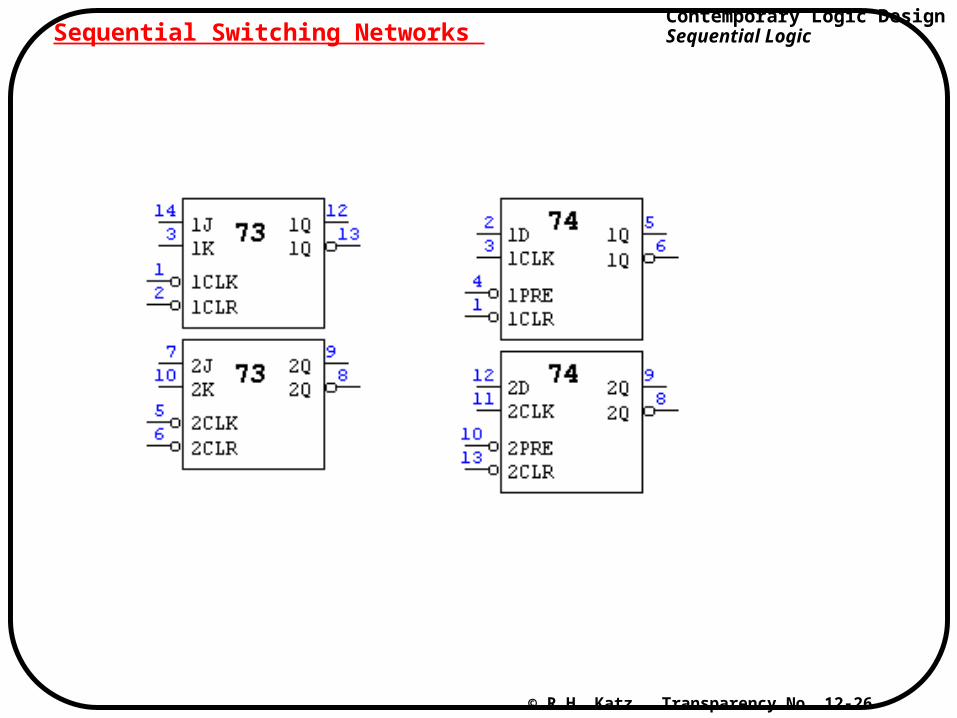
© R.H. Katz Transparency No. 12-26
Sequential Switching Networks
Contemporary Logic DesignSequential Logic
© R.H. Katz Transparency No. 12-27
HW #12 -- Section 6.1