connection parallel connection - apex … · connection parallel connection of power op ... while...
TRANSCRIPT
AN26
AN26U 1
AN26 ParallelConnection
PARALLEL CONNECTION OF POWER OP AMPSPower op amps can be paralleled to increase current, im-
prove SOA (Safe-Operating-Area), or double thermal capabil-ity. While the basic topology seems simple, there are design details which require careful attention such as common-mode range considerations, stability, slew rate, and losses which can reduce efficiency and increase power dissipation.
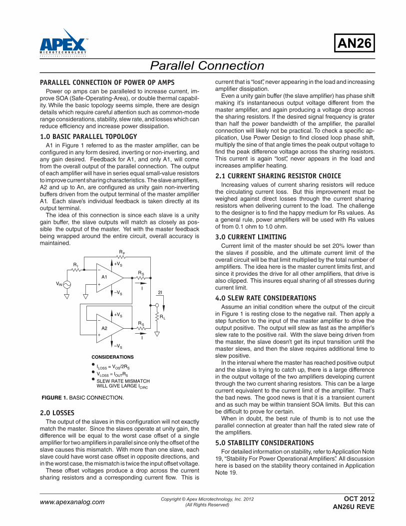
1.0 BASIC PARALLEL TOPOLOGYA1 in Figure 1 referred to as the master amplifier, can be
configured in any form desired, inverting or non-inverting, and any gain desired. Feedback for A1, and only A1, will come from the overall output of the parallel connection. The output of each amplifier will have in series equal small-value resistors to improve current sharing characteristics. The slave amplifiers, A2 and up to An, are configured as unity gain non-inverting buffers driven from the output terminal of the master amplifier A1. Each slave’s individual feedback is taken directly at its output terminal.
The idea of this connection is since each slave is a unity gain buffer, the slave outputs will match as closely as pos-sible the output of the master. Yet with the master feedback being wrapped around the entire circuit, overall accuracy is maintained.
2.0 LOSSESThe output of the slaves in this configuration will not exactly
match the master. Since the slaves operate at unity gain, the difference will be equal to the worst case offset of a single amplifier for two amplifiers in parallel since only the offset of the slave causes this mismatch. With more than one slave, each slave could have worst case offset in opposite directions, and in the worst case, the mismatch is twice the input offset voltage.
These offset voltages produce a drop across the current sharing resistors and a corresponding current flow. This is
FR
VIN
SRLR
2I
IR
I
I
SR
+VS
+VS
–VS
–VS
A1
A2
CONSIDERATIONS
ILOSS = VOS/2RS
VLOSS = IOUTRS
SLEW RATE MISMATCH WILL GIVE LARGE ICIRC
FIGURE 1. BASIC CONNECTION.
current that is “lost”, never appearing in the load and increasing amplifier dissipation.
Even a unity gain buffer (the slave amplifier) has phase shift making it’s instantaneous output voltage different from the master amplifier, and again producing a voltage drop across the sharing resistors. If the desired signal frequency is grater than half the power bandwidth of the amplifier, the parallel connection will likely not be practical. To check a specific ap-plication, Use Power Design to find closed loop phase shift, multiply the sine of that angle times the peak output voltage to find the peak difference voltage across the sharing resistors. This current is again “lost”, never appears in the load and increases amplifier heating.
2.1 CURRENT SHARING RESISTOR CHOICEIncreasing values of current sharing resistors will reduce
the circulating current loss. But this improvement must be weighed against direct losses through the current sharing resistors when delivering current to the load. The challenge to the designer is to find the happy medium for Rs values. As a general rule, power amplifiers will be used with Rs values of from 0.1 ohm to 1.0 ohm.
3.0 CURRENT LIMITINGCurrent limit of the master should be set 20% lower than
the slaves if possible, and the ultimate current limit of the overall circuit will be that limit multiplied by the total number of amplifiers. The idea here is the master current limits first, and since it provides the drive for all other amplifiers, that drive is also clipped. This insures equal sharing of all stresses during current limit.
4.0 SLEW RATE CONSIDERATIONSAssume an initial condition where the output of the circuit
in Figure 1 is resting close to the negative rail. Then apply a step function to the input of the master amplifier to drive the output positive. The output will slew as fast as the amplifier’s slew rate to the positive rail. With the slave being driven from the master, the slave doesn’t get its input transition until the master slews, and then the slave requires additional time to slew positive.
In the interval where the master has reached positive output and the slave is trying to catch up, there is a large difference in the output voltage of the two amplifiers developing current through the two current sharing resistors. This can be a large current equivalent to the current limit of the amplifier. That’s the bad news. The good news is that it is a transient current and as such may be within transient SOA limits. But this can be difficult to prove for certain.
When in doubt, the best rule of thumb is to not use the parallel connection at greater than half the rated slew rate of the amplifiers.
5.0 STABILITY CONSIDERATIONSFor detailed information on stability, refer to Application Note
19, “Stability For Power Operational Amplifiers”. All discussion here is based on the stability theory contained in Application Note 19.
Parallel Connection
AN26
Copyright © Apex Microtechnology, Inc. 2012(All Rights Reserved)www.apexanalog.com OCT 2012
AN26U REVE

AN26
2 AN26U
5.1 SLAVE STABILITYThe most obvious problem from a stability standpoint is the
unity gain buffer connection of the slaves. This configuration has the least ability to tolerate poor phase margin. Poor phase margin usually occurs as a result of excessive capacitive loading. But in the case of the PA12, the unity gain buffer connection should not be used without additional compensation. Externally compensated amplifiers should normally be compensated for unity gain and may still require additional compensation. Al-ternatively, they may be decompensated to improve slew rate and use noise gain compensation to insure stability.
The most common way we recommend to compensate the slave is with a noise gain compensation network across the inputs to the amplifier. However, for noise gain compensa-tion to work, there must be impedance in the feedback path. Figure 2 shows the modifications necessary to incorporate noise gain compensation.
The RFS value of Figure 2 is somewhat arbitrary, but its choice will dictate the final values of Rn and Cn. As is the general case in any op amp circuit, excessive impedance for RFs is something to be avoided. A realistic range of values for RFs is from 1 KΩ to 1 MΩ with a good starting point being 10 KΩ.
Once the value of RFS is pegged, noise gain compensa-tion should usually be set to give a noise gain of 10. This corresponds to Rn being one-tenth Rf. Cn must be found analytically according to procedures outlined in Application Note 19 after considering the effects of amplifier bode plot and additional poles resulting from capacitive loading. In many cases, selecting Cn for a corner frequency of 10KHz based on the value of Rn (Xcn = Rn@10KHz) will result in a stable circuit; although, analytical methods will maximize bandwidth in comparison to this method.
5.2 MASTER STABILITYA1 is subject to all normal considerations for stability. If A1
is a gain of 10 or greater, its stability will be equal to that of the slave with noise gain compensation described above. At gains below 10, the optimum noise gain will be a gain of 10 to match the slaves.
6.0 COMMON MODE CONSIDERATIONSThe unity gain buffer configuration must be able to accept
inputs equal to the maximum output swing of the master. This will be a problem with MOST amplifiers. Light loads make the situation worse. Both the output voltage swing and the common mode voltage range specifications are given as volts from the supply rail. Read the output voltage swing from the typical graph at the lowest possible current the amplifier will be required to drive when the input signal calls for saturation. Read the com-mon mode voltage specification from the specification table in the MIN column. For the parallel configuration to work without special circuitry, the output voltage swing must be at least as large as the common mode voltage specification.
The PA02 does not lend itself to parallel connection. Negative inputs which get closer than 6 volts of the negative supply rail can cause output polarity reversals which can be catastrophic in the parallel connection.
6.1 OVERCOMING COMMON MODE RESTRICTIONSA method most useful with high voltage amplifiers where
currents are low, is to simply use zener diodes in series with the supply line to the master amplifier as shown in Figure 3A. These drop the master supply low enough to restrict its output swing to be within the common-mode range of the slaves. Determine wattage ratings based on expected load + quiescent current flow.
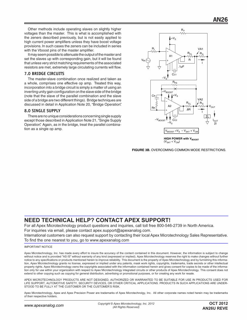
The PA04 and PA05 present another opportunity to overcome common-mode limitations by taking advantage of their boost pins. Originally incorporated to improve output voltage swing, we effectively increase common-mode range by increasing front-end supply voltages. A boost of at least 5 volts will be adequate to overcome this limitation. Figure 3B elaborates on this connection.
fR
VIN
SR
IR
I
I
SR
+VS
–VS
A1
A2
TRADITIONAL
(VSAT ≥ VCM)
FIGURE 2. SLAVE STABILITY.
ZL
RCL+
RCL–
.8R
.8R
CC2
Cn
Rn
RFS
VA2
VOUT
+VS
–VS
RCL+
CC1
RCL–
RVA1
R
VIN
IOUT2I
FR
VIN
SR
IR
I
I
SR
+VS
–VS
A1
A2
HIGH VOLTAGE(VSAT < VCM)
FIGURE 3A. OVERCOMING COMMON MODE RESTRICTIONS.
ZL
RCL
.8R
CC2
CnRn
RFS
VA2
VOUT
+VS
–VS
CC1
VA1
.1µF
IOUT2I
VRZ
VRZ.1µF
RCL
R
VRZ > VCM – VSAT
AN26
AN26U 3
VIN
SR
IR
I
I
SR
+VBOOST
–VBOOST
A1
A2
HIGH POWER with VBOOST(VSAT < VCM)
FIGURE 3B. OVERCOMING COMMON MODE RESTRICTIONS.
ZL
RCL
.8R
CC2
Cn
Rn
VA2
VOUT
+VS
–VS
CC1
VA1
.1µF
IOUT2I
RCL
R
VBOOST >VS – VSAT + VCM
–VS
+VS
FR
RFS
Other methods include operating slaves on slightly higher voltages than the master. This is what is accomplished with the zeners described previously, but is not easily applied to high current power amplifiers unless they have boost voltage provisions. In such cases the zeners can be included in series with the Vboost pins of the master amplifier.
It may seem possible to attenuate the output of the master and set the slaves up with corresponding gain, but it will be found that unless very strict matching requirements of the associated resistors are met, extremely large circulating currents will flow.
7.0 BRIDGE CIRCUITSThe master-slave combination once realized and taken as
a whole, comprises one effective op amp. Treated this way, incorporation into a bridge circuit is simply a matter of using an inverting unity gain configuration on the slave side of the bridge (note that the slave of the parallel combination and the slave side of a bridge are two different things). Bridge techniques are discussed in detail in Application Note 20, “Bridge Operation”.
8.0 SINGLE SUPPLYThere are no unique considerations concerning single supply
except those described in Application Note 21, “Single Supply Operation”. Again, as in the bridge, treat the parallel combina-tion as a single op amp.
NEED TECHNICAL HELP? CONTACT APEX SUPPORT!ForallApexMicrotechnologyproductquestionsandinquiries,calltollfree800-546-2739inNorthAmerica.Forinquiriesviaemail,pleasecontactapex.support@apexanalog.com.InternationalcustomerscanalsorequestsupportbycontactingtheirlocalApexMicrotechnologySalesRepresentative.Tofindtheonenearesttoyou,gotowww.apexanalog.comIMPORTANTNOTICE
ApexMicrotechnology,Inc.hasmadeeveryefforttoinsuretheaccuracyofthecontentcontainedinthisdocument.However,theinformationissubjecttochangewithoutnoticeandisprovided"ASIS"withoutwarrantyofanykind(expressedorimplied).ApexMicrotechnologyreservestherighttomakechangeswithoutfurthernoticetoanyspecificationsorproductsmentionedhereintoimprovereliability.ThisdocumentisthepropertyofApexMicrotechnologyandbyfurnishingthisinforma-tion,ApexMicrotechnologygrantsnolicense,expressedorimpliedunderanypatents,maskworkrights,copyrights,trademarks,tradesecretsorotherintellectualpropertyrights.ApexMicrotechnologyownsthecopyrightsassociatedwiththeinformationcontainedhereinandgivesconsentforcopiestobemadeoftheinforma-tiononlyforusewithinyourorganizationwithrespecttoApexMicrotechnologyintegratedcircuitsorotherproductsofApexMicrotechnology.Thisconsentdoesnotextendtoothercopyingsuchascopyingforgeneraldistribution,advertisingorpromotionalpurposes,orforcreatinganyworkforresale.
APEXMICROTECHNOLOGYPRODUCTSARENOTDESIGNED,AUTHORIZEDORWARRANTEDTOBESUITABLEFORUSEINPRODUCTSUSEDFORLIFESUPPORT,AUTOMOTIVESAFETY,SECURITYDEVICES,OROTHERCRITICALAPPLICATIONS.PRODUCTSINSUCHAPPLICATIONSAREUNDER-STOODTOBEFULLYATTHECUSTOMERORTHECUSTOMER’SRISK.
ApexMicrotechnology,ApexandApexPrecisionPoweraretrademarksofApexMicrotechnolgy,Inc.Allothercorporatenamesnotedhereinmaybetrademarksoftheirrespectiveholders.
Copyright © Apex Microtechnology, Inc. 2012(All Rights Reserved)www.apexanalog.com OCT 2012
AN26U REVE