switching igbts in parallel connection or with enlarged ... · switching igbts in parallel...
TRANSCRIPT

Switching IGBTs
in parallel connection or
with enlarged commutation
inductance
Thesis
Submitted to the Faculty ofElectrical- and Computer Engineering
of the Ruhr-University, Bochum
In fulfilment of the requirements for the degree
Doktor-Ingenieur
by
Burkhard Bock
Witten, Germany
Bochum, 2005

Date of Submission: May 9th, 2005
Date of Examination: July 11th, 2005
Examiner : Prof. Dr.-Ing. Andreas Steimel
Joint Examiner: Prof. Dr. phil. nat. Michael Stoisiek

i
AcknowledgementsThe results presented in this thesis were obtained during my employment as a scientificcoworker at the Institute for Electrical Power Engineering and Power Electronics (EELE)of the Ruhr-University Bochum, Germany.
I would like to thank Prof. Dr.-Ing. Andreas Steimel for supporting, accompanying andaccepting this work, and Prof. Dr. phil. nat. Michael Stoisiek for the valuable discussionsand his role as joint examiner.
Further thanks are due to:
My mentors PD Dr.-Ing. Volker Staudt and Dr.-Ing. Eberhard Krafft.
Dr.-Ing. Georg Gierse for his advice in the laboratory work.
Dr. Mark Bakran, Dr. Hans-Gunter Eckel, Dr. Martin Helsper, and Dr. Andreas Nagelfrom SIEMENS A&D for support, suggestions and discussions.
The colleagues at EELE for the good working atmosphere.
The students who supported me with their projects.
Ester Norlander for reading the manuscript.
My partner, Eva Drewermann, for support and patience.
My parents for being there.
Witten, December 16, 2005

ii

Contents iii
Contents
1 Kurzfassung 1
2 Preface 3
3 Introduction 53.1 Power Electronics . . . . . . . . . . . . . . . . . . . . . . . . . . . . . . . . 53.2 Power-electronic switches . . . . . . . . . . . . . . . . . . . . . . . . . . . . 53.3 Power semiconductor devices . . . . . . . . . . . . . . . . . . . . . . . . . . 6
3.3.1 Basics . . . . . . . . . . . . . . . . . . . . . . . . . . . . . . . . . . 63.3.2 Power Diodes . . . . . . . . . . . . . . . . . . . . . . . . . . . . . . 8
3.3.2.1 Power diode basics . . . . . . . . . . . . . . . . . . . . . . 83.3.2.2 Power diode turn-on . . . . . . . . . . . . . . . . . . . . . 93.3.2.3 Power diode turn-off . . . . . . . . . . . . . . . . . . . . . 9
3.3.3 Bipolar switching devices . . . . . . . . . . . . . . . . . . . . . . . . 103.3.4 Unipolar switching devices . . . . . . . . . . . . . . . . . . . . . . . 113.3.5 Power MOS-bipolar devices . . . . . . . . . . . . . . . . . . . . . . 11
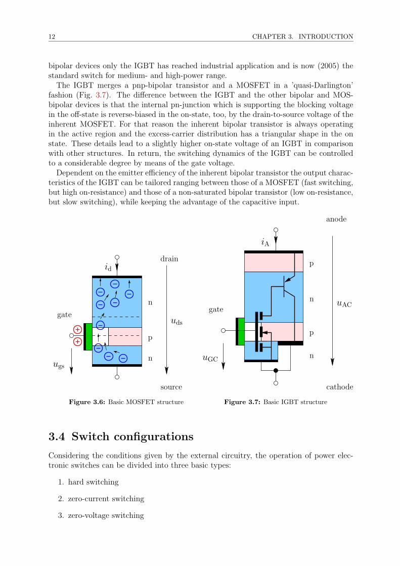
3.4 Switch configurations . . . . . . . . . . . . . . . . . . . . . . . . . . . . . . 123.5 Generic hard-switch waveforms . . . . . . . . . . . . . . . . . . . . . . . . 14
3.5.1 Generic hard-switch turn-on . . . . . . . . . . . . . . . . . . . . . . 143.5.2 Generic hard-switch turn-off . . . . . . . . . . . . . . . . . . . . . . 15
4 IGBT 174.1 Basic operation . . . . . . . . . . . . . . . . . . . . . . . . . . . . . . . . . 174.2 Static output characteristics . . . . . . . . . . . . . . . . . . . . . . . . . . 194.3 Internal capacitances . . . . . . . . . . . . . . . . . . . . . . . . . . . . . . 214.4 Anode-current to gate-voltage feedback . . . . . . . . . . . . . . . . . . . . 25
4.4.1 Underlying mechanism . . . . . . . . . . . . . . . . . . . . . . . . . 254.4.2 Setup for practical examination . . . . . . . . . . . . . . . . . . . . 264.4.3 Measurements . . . . . . . . . . . . . . . . . . . . . . . . . . . . . . 27
4.5 Base resistance . . . . . . . . . . . . . . . . . . . . . . . . . . . . . . . . . 324.6 IGBT switching waveforms . . . . . . . . . . . . . . . . . . . . . . . . . . . 34
4.6.1 Switching condition . . . . . . . . . . . . . . . . . . . . . . . . . . . 344.6.2 Turn-on . . . . . . . . . . . . . . . . . . . . . . . . . . . . . . . . . 374.6.3 Turn-off . . . . . . . . . . . . . . . . . . . . . . . . . . . . . . . . . 42
4.7 Latch-Up . . . . . . . . . . . . . . . . . . . . . . . . . . . . . . . . . . . . 464.8 Short circuit . . . . . . . . . . . . . . . . . . . . . . . . . . . . . . . . . . . 484.9 IGBT gate-drive requirements . . . . . . . . . . . . . . . . . . . . . . . . . 50
4.9.1 Static off-state . . . . . . . . . . . . . . . . . . . . . . . . . . . . . 50

iv Contents
4.9.2 Static on-state . . . . . . . . . . . . . . . . . . . . . . . . . . . . . . 504.9.3 Turn-on . . . . . . . . . . . . . . . . . . . . . . . . . . . . . . . . . 51
4.10 Turn-off . . . . . . . . . . . . . . . . . . . . . . . . . . . . . . . . . . . . . 51
5 IGBT design 535.1 P-Channel IGBT . . . . . . . . . . . . . . . . . . . . . . . . . . . . . . . . 535.2 Switching speed enhancement . . . . . . . . . . . . . . . . . . . . . . . . . 535.3 Lifetime control . . . . . . . . . . . . . . . . . . . . . . . . . . . . . . . . . 545.4 Emitter efficiency . . . . . . . . . . . . . . . . . . . . . . . . . . . . . . . . 545.5 Punch-through IGBT . . . . . . . . . . . . . . . . . . . . . . . . . . . . . . 545.6 Non-punch-through IGBT . . . . . . . . . . . . . . . . . . . . . . . . . . . 565.7 Soft-punch-through / field-stop IGBT . . . . . . . . . . . . . . . . . . . . . 575.8 Injection Enhancement . . . . . . . . . . . . . . . . . . . . . . . . . . . . . 575.9 Trench gate . . . . . . . . . . . . . . . . . . . . . . . . . . . . . . . . . . . 585.10 Temperature dependence . . . . . . . . . . . . . . . . . . . . . . . . . . . . 60
6 Parallelled IGBTs 616.1 Introduction . . . . . . . . . . . . . . . . . . . . . . . . . . . . . . . . . . . 616.2 Theory of parallelled IGBTs . . . . . . . . . . . . . . . . . . . . . . . . . . 62
6.2.1 Basis of discussion . . . . . . . . . . . . . . . . . . . . . . . . . . . 626.2.2 Turn-on of parallelled IGBTs . . . . . . . . . . . . . . . . . . . . . 626.2.3 Turn-off of parallelled IGBTs . . . . . . . . . . . . . . . . . . . . . 65
6.3 Deviating commutation inductance . . . . . . . . . . . . . . . . . . . . . . 666.3.1 Motivation . . . . . . . . . . . . . . . . . . . . . . . . . . . . . . . . 666.3.2 Test conditions . . . . . . . . . . . . . . . . . . . . . . . . . . . . . 67
6.3.2.1 Turn-on of parallelled IGBT modules . . . . . . . . . . . . 676.3.2.2 Turn-off of parallelled IGBT modules . . . . . . . . . . . . 706.3.2.3 Turn-on of parallelled diodes . . . . . . . . . . . . . . . . 726.3.2.4 Turn-off of parallelled diodes . . . . . . . . . . . . . . . . 726.3.2.5 Conclusion . . . . . . . . . . . . . . . . . . . . . . . . . . 75
6.4 Chips parallelled inside a press-pack IGBT (PPI) device . . . . . . . . . . 766.4.1 Test conditions . . . . . . . . . . . . . . . . . . . . . . . . . . . . . 766.4.2 Turn-on of parallelled PPI chips . . . . . . . . . . . . . . . . . . . . 766.4.3 Turn-off of parallelled IGBTs . . . . . . . . . . . . . . . . . . . . . 826.4.4 Simulations . . . . . . . . . . . . . . . . . . . . . . . . . . . . . . . 88
6.4.4.1 SPICE model . . . . . . . . . . . . . . . . . . . . . . . . . 886.4.5 Simulation of turn-on . . . . . . . . . . . . . . . . . . . . . . . . . . 896.4.6 Simulation of turn-off . . . . . . . . . . . . . . . . . . . . . . . . . . 94
6.5 Conclusions . . . . . . . . . . . . . . . . . . . . . . . . . . . . . . . . . . . 98
7 Converter with large commutation inductance 997.1 Multi-commutation in complex inverter systems . . . . . . . . . . . . . . . 99
7.1.1 Experimental approach . . . . . . . . . . . . . . . . . . . . . . . . . 1007.2 Turn-off with large commutation inductance . . . . . . . . . . . . . . . . . 101
7.2.1 Requirements for a safe turn-off . . . . . . . . . . . . . . . . . . . . 1017.2.2 Limiting the overvoltage of ’field-stop’ IGBTs . . . . . . . . . . . . 1017.2.3 Comparison of NPT-type and ’field-stop’ IGBTs . . . . . . . . . . . 104

Contents v
7.2.4 Conclusion . . . . . . . . . . . . . . . . . . . . . . . . . . . . . . . . 1107.3 Turn-on with large commutation inductance . . . . . . . . . . . . . . . . . 111
7.3.1 Influence of the commutation inductance on the turn-on waveforms 1117.3.2 Active diode snubbing (ADS) . . . . . . . . . . . . . . . . . . . . . 1137.3.3 Experimental setup for ADS . . . . . . . . . . . . . . . . . . . . . . 1157.3.4 Measurements . . . . . . . . . . . . . . . . . . . . . . . . . . . . . . 116
7.3.4.1 Active snubbing of the diode with negative static gate biasfor the antiparallel IGBT . . . . . . . . . . . . . . . . . . 116
7.3.4.2 Active snubbing of the diode with zero static gate bias forthe antiparallel IGBT . . . . . . . . . . . . . . . . . . . . 123
7.3.4.3 Comparison with moderated conventional turn-on . . . . . 1277.3.5 Conclusion . . . . . . . . . . . . . . . . . . . . . . . . . . . . . . . . 133
8 Summary 135
A Additional measurements and simulations 137
B Power-electronic measurements 153B.1 Data acquisition . . . . . . . . . . . . . . . . . . . . . . . . . . . . . . . . . 153B.2 Measures against electromagnetic interferences . . . . . . . . . . . . . . . . 153
B.2.1 Sources of interference . . . . . . . . . . . . . . . . . . . . . . . . . 153B.2.2 Common impedance . . . . . . . . . . . . . . . . . . . . . . . . . . 154B.2.3 Capacitive coupling (du/dt-interference) . . . . . . . . . . . . . . . 154B.2.4 Inductive coupling (di/dt-interference) . . . . . . . . . . . . . . . . 155B.2.5 Jumping reference potential . . . . . . . . . . . . . . . . . . . . . . 155
B.3 Improving power-electronic measurements . . . . . . . . . . . . . . . . . . 157B.3.1 Motivation . . . . . . . . . . . . . . . . . . . . . . . . . . . . . . . . 157B.3.2 Test setup . . . . . . . . . . . . . . . . . . . . . . . . . . . . . . . . 157B.3.3 Measurements . . . . . . . . . . . . . . . . . . . . . . . . . . . . . . 158B.3.4 Discussion . . . . . . . . . . . . . . . . . . . . . . . . . . . . . . . . 162
B.4 Current measurement . . . . . . . . . . . . . . . . . . . . . . . . . . . . . . 165B.4.1 Current probes . . . . . . . . . . . . . . . . . . . . . . . . . . . . . 165B.4.2 High-frequency coaxial shunt . . . . . . . . . . . . . . . . . . . . . . 165B.4.3 Rogowski coils . . . . . . . . . . . . . . . . . . . . . . . . . . . . . . 167
B.4.3.1 Rogowski coil basics . . . . . . . . . . . . . . . . . . . . . 167B.4.3.2 Dynamic characteristic of the Rogowski coil . . . . . . . . 168B.4.3.3 The EELE Rogowski coil . . . . . . . . . . . . . . . . . . 169B.4.3.4 Compensating perpendicular fields . . . . . . . . . . . . . 169B.4.3.5 A/D converter noise . . . . . . . . . . . . . . . . . . . . . 173
B.4.4 Qualification of current probes . . . . . . . . . . . . . . . . . . . . . 175
Bibliography 179

List of symbols
General Abbreviations
ADS Active Diode SnubbingEMC Electromagnetic EompatibilityGTO Gate Turn-Off ThyristorIGBT Insulated Gate Bipolar TransistorIEGT Injection Enhanced Gate Transistori intrinsic (semiconductor)JFET Junction Field Effect TransistorMOSFET Metal-Oxide-Semiconductor
Field Effect Transistorn n-dopded (semiconductor)PPI Press Pack IGBTp p-dopded (semiconductor)
Components
C capacitorD diodeJ junction (semiconductor device)L inductorR resistorS switchT transistor
Quantities
A areaB current gain (bipolar transistor)C capacityE electric field strengthe elementary chargef frequencyg transconductanceH magnetic field strengthI rms currenti instantaneous currentk factorL inductivityl lengthM mutual inductivityN doping concentrationn negative doping concentrationp positive doping concentrationR resistancer radiust timeU rms value of voltageu instantaneous value of voltagev velocityW channel width (MOSFET)w width or
number of turns (coil)
x distanceZ impedancebeta differential current gainγ emitter efficiencyε permittivityϑ temperatureλ wavelengthµ mobility (semiconductor)ρ charge densityτ excess-carrier lifetimeφ electric potentialψ magnetic flux
Subscripts
A anode (semiconductor device) orantiparallel (converter)
B blocking (semiconductor)b base (bipolar transistor) or
body (MOSFET)bus dc-link busbarbd break down (semiconductor)bi built-in (semiconductor)c collector (bipolar transistor) or
centre (coaxial cable)ch channel (MOSFET)com commutation (converter)coup couplingcrit criticalD donator (semiconductor)d drain (MOSFET) or
delay (switching transients)d dc-link (converter)depl depletion layerdispl displacemente emitter (bipolar transistor)ext externalfb feedbackG gate (semiconductor device)GD gate drive (IGBT)g gate (semiconductor structure)gr groundh hole (semiconductor)i internal or
induced (Rogowski coil)JFET JFETj junction (semiconductor)load loadm specific number or
metallisation (MOSFET) orMOSFET (transconductance) ormeasured (Rogowski coil)

max maximumn another specific number or
negative carriers (semiconductor)nom nominalon on state (semiconductor device) or
on transient (semiconductor device)off off state (semiconductor device) or
off transient (semiconductor device)out outputox oxide (MOSFET)p positive carriers (semiconductor)ph phasepnp pnp-transistorq between conductorsr reverse (semiconductor device) or
redistribution (IGBT)rms root-mean-square valueS shuntings source (MOSFET) or
screen (coaxial cable)scope oscilloscopeswitch switch (generic)t terminating or
total (reverse current)th threshold (MOSFET)VP voltage probez zener elementν unspecified numberσ distributed (inductance)
Superscripts
+ high-doped (semiconductor)− low-doped (semiconductor)’ per unit area or
specific (commutation inductance)* calculated (Rogowski coil)
Above an expression
x derivative with respect to timex peak value of a quantityx mean value of a quantity


1
1 Kurzfassung
Schaltverhalten von IGBTs in Parallelschaltungenund bei erhohter Kommutierungsinduktivitat
Der Insulated Gate Bipolar Transistor (IGBT) ist heute (2005) der am weitesten ver-breitete Halbleiterschalter fur selbstgefuhrte leistungselektronische Schaltungen. Er zeich-net sich dadurch aus, dass Spannungs- und Stromflanken weitgehend uber den Steuerein-gang, das ’gate’, beeinflussbar sind.
IGBT-Schaltvorgange werden in der Literatur bisher anhand des Ausgangskennlin-ienfeldes des Bauelementes beschrieben. Dieses wird als Stromquelle aufgefasst, welchedurch die ’gate’-Spannung gesteuert wird. Der Einfluss der Induktivitat in der Kommu-tierungsmasche (Kommutierungsinduktivitat) wird dabei als parasitarer Effekt zweiterOrdnung betrachtet. Obwohl diese Darstellung fur eine elementare Beschreibung derSchaltvorgange ausreichend ist, erschwert sie doch eine genaue Analyse, da in Bezug aufdie Spannung an der Kommutierungsinduktivitat Ursache und Wirkung vertauscht wer-den.
In dieser Arbeit wird daher eine Beschreibung der IGBT-Schaltvorgange vorgeschlagen,welche die Kommutierungsspannung als bestimmende Große fur die Stromgradienten inden Vordergrund stellt. Dabei werden drei wesentliche Mechanismen einbezogen, diefur sich bekannt sind, aber normalerweise bei der Beschreibung der Schalttransientenaußer acht gelassen werden: Die Ruckwirkung des Anodenstrombetrages auf die ’gate’-Kathoden-Spannung, die Auswirkung mobiler Ladungstrager in der Raumladungszoneauf die Sperrschichtspannung sowie die Dynamik der Speicherladung.
Auf Basis der so vervollstandigten Modellvorstellung des IGBT wird die Parallelschal-tung von IGBTs untersucht. Dabei wird sowohl die Parallelschaltung einzelner Bauele-mente als auch die Parallelschaltung einzelner Chips in einem Bauelement betrachtet. Ausder Analyse von Messungen konnen die Ursachen fur ungleiche stationare Stromaufteilun-gen und dynamische Umverteilungen des Gesamtstroms wahrend der Schaltflanken deneinzelnen Modellbestandteilen zugeordnet werden.
Eine weitere technische Herausforderung, die ein vertieftes Verstandnis des IGBT-Schaltverhaltens erfordert, ist das Schalten von so genannten Feldstopp-IGBTs bei erhohterKommutierungsinduktivitat. Feldstopp-Bauelemente konnen ihre Ausgangscharakteristikwahrend des Ausschaltvorganges drastisch andern, was besondere Anforderungen an dieAnsteuerung stellt. Es wird gezeigt, wie Feldstopp-IGBTs wirkungsvoll vor zerstorerischenUberspannungen beim Schalten mit erhohter Kommutierungsinduktivitat geschutzt wer-den konnen. Ein Vergleich mit IGBTs einer alteren Generation zeigt, dass die spezifischenVorteile des untersuchten Feldstopp-IGBTs in Bezug auf die Ausschaltverluste durch dieerforderlichen Vorkehrungen zum Uberspannungsschutz marginalisiert werden.
Die Freilauf- oder Ruckarbeitsdioden des Umrichters werden bei deutlich erhohter Kom-mutierungsinduktivitat einer unzulassigen Belastung ausgesetzt. Hier gilt es, den Max-imalwert der Augenblicksleistung zu begrenzen, der mit dem Auftreten von ’avalanche’-

2 CHAPTER 1. KURZFASSUNG
Multiplikation verknupft ist. Zu diesem Zweck wird eine aktive Ausschaltentlastung derDiode (’active diode snubbing’, ADS) durch den antiparallelen IGBT untersucht. Dieseneue Technik stellt bei erhohter Kommutierungsinduktivitat eine Alternative zur Ver-langsamung des IGBT-Einschaltvorganges dar. Es zeigt sich aber im Vergleich, dassdie aktive Schaltentlastung der Diode nur bei großen Laststrommittelwerten zu geringenGesamtschaltverlusten fuhrt.
Diese Aussagen werden mit umfangreichen Messungen belegt. Handelsubliche Mess-mittel wurden nach Analyse der fur leistungselektronische Schaltungen spezifischen Stor-mechanismen durch besondere Abschirmungsmaßnahmen verbessert. Daruber hinauswurden Hochfrequenz-Koaxialshunts und Rogowskispulen entworfen, deren dynamischeEigenschaften denen kommerziell erhaltlicher Messmittel uberlegen sind.

3
2 Preface
The Insulated Gate Bipolar Transistor (IGBT) is today (2005) a popular power semicon-ductor device which is available for maximum blocking voltages ranging between 600 Vand 6500 V. For reasons of marketing, in many publications a relatively simple descrip-tion of the transient characteristics of the IGBT is used to emphasise that IGBT are easyto deal with. This simplified description uses characteristic curves for the description ofswitching waveforms. Thereby the IGBT is regarded as a current source that is controlledby the gate-to-cathode voltage. The impact of the stray inductance in the commutationloop (commutation inductance) is treated as a second-order effect. While this is a viableapproach to attain a rough description of the switching transients, it is not suitable for ain-depth analysis of switching waveforms since cause and effect are confused with respectto the voltage at the commutation inductance.
Applying IGBTs, challenges arise for example from parallel connections or from the op-eration with enlarged commutation inductance. The application of commercially availableIGBT devices in these scenarios requires an in-depth understanding of the IGBT dynam-ics. Though many detailed descriptions of the transient characteristics of the IGBT havebeen published, these publications usually provide complex mathematical models the pa-rameters of which are not available for the user. In addition, the behaviour of the deviceis mostly described implicitly by differential equations. On the other hand the user of thedevices needs a qualitative understanding of the dynamics of IGBTs that covers all effectsrelevant for the converter design.
This work gives a predominantly verbal explanation of all aspects of IGBT charac-teristics that are relevant for a detailed discussion of IGBT switching waveforms. Incontrast to other publications, the description of the switching transients focuses on thecommutation voltage which is the fundamental quantity for all switching processes. Theanode-current to gate-voltage feedback, the impact of mobile carriers in the depletionlayer, and the dynamics of the base resistance are included into the description of thetransient characteristics.
On basis of this understanding of the IGBT the parallel operation of IGBTs is analysedwhile the examinations are focused on the inhomogeneities caused by the spread of thedevice parameters. The causes for uneven current distributions in the static case anddynamic redistributions during the switching transients that can be observed in measure-ments are assigned to the responsible parts of the IGBT model.
Furthermore, the operation of ’field stop’ IGBTs at enlarged commutation inductanceas encountered in large inverter systems in case of simultaneous switching of several pairsof arms is analysed. When switched with a large commutation inductance, ’field stop’devices can show a drastic change in their output characteristic during turn-off whichmakes it challenging to prevent destructive overvoltages by means of the gate drive. It isshown that the switching speed of ’field stop’ IGBTs has to be reduced significantly toenable an active clamping. In case of a large commutation inductance this increases theturn-off losses and thus impairs the advantage of ’field stop’ IGBTs over NPT IGBTs of

4 CHAPTER 2. PREFACE
older device generations.The stress of the regenerating diodes of an inverter, too, is increased in case of a large
commutation inductance. A new technique to keep the safe operation area of the diodeis Active Diode Snubbing (ADS) by means of the antiparallel IGBT. This method isinvestigated as an alternative to simply slowing down the switching speed of the IGBTturning on.
The practical examinations reported in this work required an improvement of the con-ventional measurement techniques which is outlined in the Appendix. This also includedthe development of high-frequency shunts and Rogowski coils the dynamic characteristicsof which are superior to those commercially available.

5
3 Introduction
3.1 Power Electronics
The task of power electronics is to direct the flow of electrical energy between two electricalsystems. In the general (and practically most often) case voltage, 1 frequency and numberof conductors of the systems to be linked are not identical, so that a converter is neededto enable the connection. This converter controls the exchange of electrical energy bysupplying appropriate voltages and currents at the terminals (Fig. 3.1).
System 1 System 2Converter
1
n
1
m
PSfrag replacements
u1ν u2ν
f1 f2
Figure 3.1: Power-electronic converter linking two electrical systems with voltages u1ν , frequency f1and number of conductors n on the one side and u2ν , f2 and m on the other side.
The control of the flow of electrical energy at the intersection of the systems joinedtogether is mostly aimed at the net flow of energy over a certain period of time. Apartfrom that it may also have the goal to achieve favourable instantaneous currents andvoltages.
For high power applications, converter losses have to be strictly minimised. This is notonly because of the cost of energy, but especially for thermal reasons and the associatedcost for cooling. Doing this the only feasible strategy is to use switch-mode converterswhich theoretically operate without losses since ideally either the voltage or the current ofa switch is zero. Switching operation implies that the average output (voltage or current)over one switching period has the desired magnitude whereas the instantaneous values ofthe output differ at nearly any instant. This generally requires filtering elements whichmay be contained in the load characteristics. Furthermore, the switching frequency atminimum must be as high as the frequency of the output voltage, generally a multiplehigher.
3.2 Power-electronic switches
At first glance switches qualified for power electronic applications should
• have a negligible on-resistance to minimise conduction losses,
1It is well known that quantities and their values have to be discerned. However, for the sake ofreadability, the term ’value’ is omitted here if it is clear from the context that the value of a quantityand not the quantity itself is referred to.

6 CHAPTER 3. INTRODUCTION
• have a negligible leakage current in the off-state ,
• block sufficiently large voltages,
• switch fast to minimise switching losses,
• switch without delay,
• require low driving power2,
• withstand high temperatures, and
• have a high reliability.
While on the one hand fast switching, thus steep current and voltage transients arenecessary to minimise losses and effort for filtering, on the other hand current and voltageslopes often have to be limited in order to fulfil requirements of electromagnetic compati-bility (EMC) and to reduce the stress of the insulation. In order to reduce the number ofcomponents of a converter to the benefit of reliability, preferably the switch itself shouldbe able to limit current and voltage slopes to a tolerable maximum.
Furthermore, to facilitate the handling of short-circuit situations, it is desirable that theswitch limits short-circuit currents by a largely increasing on-state voltage at overcurrents.
Since it is often required to operate many switches in parallel to achieve the desired cur-rent capability, a positive temperature coefficient of the on-resistance is strongly requiredto balance the total current among the single switches.
3.3 Power semiconductor devices
3.3.1 Basics
Suitable state-of-the-art switches are semiconductor devices optimised for switching ap-plications, often called power semiconductors or power devices. The blocking voltage ofa power semiconductor switch is supported by a reverse-biased pn-junction (Figure 3.2).The charge density ρ in the depleted semiconductor on either sides of the junction resultsfrom the respective doping concentration.
For an one-dimensional analysis the electric field strength E is derived by integratingPoisson’s equation:
d2φ(x)
dx= −ρ(x)
εs
(3.1)
⇒ E =1
ε
∫
ρ · dx (3.2)
where φ is the electric potential and εs the permittivity of the semiconductor. The mag-nitude of the electric field before breakdown inside silicon is limited to
Ecrit = 4010 · ND
cm3
1/8
[V/m] [3] (3.3)
2Decreasing the driving power increases the risk of an unintended switching triggered by interferencefrom the power electronic circuit. For that reason, a minimum driving power is desirable.

3.3. POWER SEMICONDUCTOR DEVICES 7
PSfrag replacements
p+
p
n+
n−
n
uB
i
ρ E =∫
ρ · dx
Emax
uB =∫
E · dx
space charge density electric field strength
xx
Figure 3.2: Blocking voltage of a pn-junction (one-dimensional model)
with ND being the homogeneous donator doping density. equation(3.3) assumes an abruptpn-junction with the doping concentration of the p-side being much higher than the dopingconcentration of the n-side. However, high-energy particles of cosmic rays can cause thebreakdown of a pn-junction in the blocking state [128]. The probability of a failureinduced by cosmic rays increases with the peak electric field strength in the depletionlayer and with device area. For that reason the maximum electrical field strength inpower semiconductor devices has to be chosen considerably lower than Ecrit to achieveacceptable failure rates.
To maximise the blocking voltage
uB =
∫
wdepl
E · dx (3.4)
(which is equivalent to the area under the curve of the electric field strength (fig. 3.2))without exceeding Ecrit, the gradient of the electric field, thus the dopant concentrationmust be small on at least one side of the junction. Consequently the structure of everysemiconductor switch with high blocking voltage contains a wide, low-doped region oftenreferred to as ’drift region’ because of its high resistivity. 3
A simple pn-junction exhibits the function of a diode the current and voltage of whichare determined by the external circuit. The power diode, which is inherent in the structureof every semiconductor switch, is discussed in Section 3.3.2. To build a controllableswitch, the pn-junction that is blocking the off-state voltage has to be ’shorted’ to turnon the device. This can be done using two different mechanisms represented by thebipolar transistor and the MOSFET which are discussed briefly in Sections 3.3.4 and3.3.5, respectively.
3Actually the net doping concentration of the depleted region has to be low. Multi-junction deviceslike the COOLMOS [65] feature vertical p-strips in a n−-drift region. This allows for a higher dopingconcentration in the n-strips which carry the current in the on-state. In the blocking state, the chargein the p-strips compensates for part of the charge in the n-strips.

8 CHAPTER 3. INTRODUCTION
3.3.2 Power Diodes
3.3.2.1 Power diode basics
Diodes are needed as regenerating diodes or freewheeling diodes in virtually every oftoday’s (2005) power electronic circuits. The design of power diodes must ensure a highblocking voltage and a low conduction voltage. Diodes for power electronic circuits inaddition must show a good switching behaviour, i.e. the transition from the on-state to theoff-state must be ’fast’ without producing excessive overvoltages at parasitic inductances.
As seen in Section 3.3.1 a high blocking voltage requires a wide drift region which isusually n-doped. In the on-state, the otherwise highly resistive drift region is floodedwith minority carriers injected across the junction according to the emitter efficency ofthe junction. This reduces the on-resistance of the diode. To enhance carrier injection inthe on-state, power diodes always have a high-doped cathode which injects electrons intothe drift region when the diode is forward-biased. This structure is referred to as p-i-ndiode (i for intrinsic, Fig. 3.3). If the width of the drift zone is in the order of magnitudeof the ambipolar diffusion length, the excess-carrier concentration in the on-state easilyexceeds the intrinsic carrier concentration, which is referred to as ’high-level injection’.
For turn-off, the excess carriers have to be removed to bring the diode into the blockingstate. The removal of the excess carriers slows down the switching speed. Thus at a givenblocking voltage level a trade-off exists between switching speed and on-resistance. Thistrade-off can be improved by applying a so-called ’punch-through’ design which meansthat the whole drift region is depleted in the blocking state so that the electric field’punches through’ the drift region. Because of the considerably higher doping of anodeand cathode, the shape of the electric field takes a trapezoidal shape when the diode is inthe blocking state. This is illustrated in Figure 3.3. With the area under the curve of the
PSfrag replacements
p+
p+
n+
n−
n
uB
i
ρ E =∫
ρ · dx
Emax
uB =∫
E · dx
space charge density electric field strength
xx
Figure 3.3: Punch-through diode in the blocking state (one-dimensional model)
electric field strength at a given peak electric field strength thus increased, the width ofthe drift region can be decreased. This reduces both the amount of excess-carrier chargeand the on-resistance.

3.3. POWER SEMICONDUCTOR DEVICES 9
3.3.2.2 Power diode turn-on
As mentioned in the previous Section, the major part of the charge carrying the currentin the drift region is provided by injection. However, when the diode starts to conductcurrent, it takes some time to build up the excess-carrier charge in the drift region, whichis referred to as ’forward recovery’. Hence the differential resistance is quite high in thefirst instant when the diode takes over current, which results in a significant voltage dropfor the duration of a few microseconds.
3.3.2.3 Power diode turn-off
Non-ideal current and voltage waveforms related to the turn-off of a diode are called’reverse recovery’. To bring the diode into the blocking state, the excess carriers injectedinto the drift region in the on-state have to be removed. Since the decay of the storedcharge due to recombination takes several microseconds, the greatest part has to be ’sweptout’ by a reverse current to achieve acceptable switching times. The reverse current usuallycauses additional losses in other circuit elements which have to take over this current inaddition to the load current. The diode starts to support blocking voltage as soon as theexcess-carrier density at the pn-junction has decreased to zero. The corresponding chargewhich has to be removed until the voltage starts to rise is called ’stored charge’.
However, excess carriers remain in the undepleted drift region while the blocking voltageis built up and the depletion layer widens. Thus a minority-carrier current which doesnot contribute to the build-up of the blocking voltage is present in the undepleted driftregion during the voltage ramp. Hence, the non-linear output capacitance of the diodeduring turn-off
Cout =iDduD
dt
(3.5)
depends on the excess-carrier charge which is determined by the value of the initial forwardcurrent and the conduction time.
During the build-up of the diode voltage the output capacitance of the diode decreasesdue to the growing width of the depletion layer (thus increasing width of the space-chargecapacitance) and due to the recombination of the excess-carrier charge. A small seriesstray inductance, which is present in every real circuit and which supports the reversecurrent, can therefore cause significant overvoltages. If the non-linear output capacitanceof the diode decreases significantly at the end of the turn-off process, the remaining reversecurrent leads to a steep increase of the diode voltage. Since the overvoltage of the diodeadds to the commutation voltage at the stray inductance, this brings the reverse currentto zero very quickly which is referred to as a ’snap-off’ which usually leads to severeoscillations and therefore is not desirable. In case of an excessive overvoltage the diode isdestroyed. The design of the diode thus has to ensure a moderate increase of the diodevoltage by avoiding a too sudden decay of the output capacitance during turn-off.
Minority carriers traversing the depletion layer while the voltage is built up add tothe background doping concentration, which enlarges the magnitude of the electric fieldstrength and thus the voltage across the depletion layer. Therefore the diode voltagemay decrease in spite of a still negative current when the value of the reverse currentdecreases. During reverse recovery, avalanche multiplication can occur if the critical
10 CHAPTER 3. INTRODUCTION
electric field strength is exceeded due to the charge of mobile minority carriers in thespace-charge region. It can be shown that the onset point of the dynamic avalanchemultiplication depends upon the power density of the diode (e.g. [48]). The critical powerdensity amounts to approximately Pcrit = 200 kW/cm2. While avalanche multiplicationtheoretically is a self-limiting process, inhomogeneities in the semiconductor can lead tothe breakdown of the device [24].
3.3.3 Bipolar switching devices
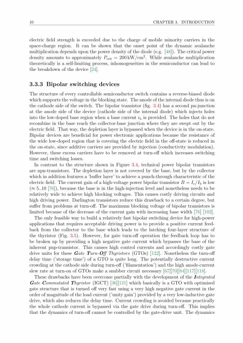
The structure of every controllable semiconductor switch contains a reverse-biased diodewhich supports the voltage in the blocking state. The anode of the internal diode thus is onthe cathode side of the switch. The bipolar transistor (fig. 3.4) has a second pn-junctionat the anode side of the device (cathode side of the internal diode) which injects holesinto the low-doped base region when a base current ib is provided. The holes that do notrecombine in the base reach the collector-base junction where they are swept out by theelectric field. That way, the depletion layer is bypassed when the device is in the on-state.Bipolar devices are beneficial for power electronic applications because the resistance ofthe wide low-doped region that is covering the electric field in the off-state is reduced inthe on-state, since additive carriers are provided by injection (conductivity modulation).However, these excess carriers have to be removed at turn-off which increases switchingtime and switching losses.
In contrast to the structure shown in Figure 3.4, technical power bipolar transistorsare npn-transistors. The depletion layer is not covered by the base, but by the collectorwhich in addition features a ’buffer layer’ to achieve a punch-through characteristic of theelectric field. The current gain of a high-voltage power bipolar transistor B = Ic/Ib is low(≈ 5..10 [76]), because the base is in the high-injection level and nonetheless needs to berelatively wide to achieve high blocking voltages. This causes costly driving circuits andhigh driving power. Darlington transistors reduce this drawback to a certain degree, butsuffer from problems at turn-off. The maximum blocking voltage of bipolar transistors islimited because of the decrease of the current gain with increasing base width [76] [102].
The only feasible way to build a relatively fast bipolar switching device for high-powerapplications that requires acceptable driving power is to provide a positive current feed-back from the collector to the base which leads to the latching four-layer structure ofthe thyristor (Fig. 3.5). However, for gate turn-off operation the feedback loop has tobe broken up by providing a high negative gate current which bypasses the base of theinherent pnp-transistor. This causes high control currents and accordingly costly gatedrive units for these Gate Turn-Off Thyristors (GTOs) [122]. Nonetheless the turn-offdelay time (’storage time’) of a GTO is quite long. The potentially destructive currentcrowding at the cathode side during turn-off (’filamentation’) and the high anode-currentslew rate at turn-on of GTOs make a snubber circuit necessary [67][70][84][117][118].
These drawbacks have been overcome partially with the development of the IntegratedGate Commutated Thyristor (IGCT) [36][121] which basically is a GTO with optimisedgate structure that is turned off very fast using a very high negative gate current in theorder of magnitude of the load current (’unity gain’) provided by a very low-inductive gatedrive, which also reduces the delay time. Current crowding is avoided because practicallythe whole cathode current is bypassed via the gate drive during turn-off. This impliesthat the dynamics of turn-off cannot be controlled by the gate-drive unit. The dynamics

3.3. POWER SEMICONDUCTOR DEVICES 11
of turn-on are determined by the internal feedback loop. Especially the fast turn-on ofIGCTs causes high reverse recovery stress for the diode, which usually necessitates aturn-on snubber. [22].
PSfrag replacementsbase
ib
ic
emitter
collector
uce
p
p
n
Figure 3.4: Basic pnp-transistor structure
PSfrag replacements
anode
cathode
uAC
iA
iG
gate
p
p
n
n
Figure 3.5: Basic thyristor/GTO structure
3.3.4 Unipolar switching devices
At turn-on the MOSFET depicted in Figure 3.6 shorts the pn-junction which is supportingthe blocking voltage by inversion of the semiconductor doping type through applicationof an electric field via the gate electrode. MOS devices show a capacitive input so thattheoretically the mean driving power is zero. Since the current is only carried by majoritycarriers, the switching speed is high. On the other side the absence of conductivitymodulation due to additive minority carriers in the low-doped region that is covering theelectric field in the off-state leads to a very high on-resistance. The dependence of theon-resistance Ron on the breakdown voltage ubd is approximately given by [47]
Ron ≈ 3.7 · 10−9 Ωcm2
A·(ubd
V
)2.6
(3.6)
with A being the device area. For that reasons unipolar power devices are not suitablefor high-power applications which require devices with high blocking voltage (> 800 V).
3.3.5 Power MOS-bipolar devices
To avoid the specific drawbacks of bipolar devices (slow switching speed, expensive gatedrive) and of unipolar devices (high on-resistance), several hybrid structures have beenproposed including the MOS Controlled Thyristor, (MCT), the MOS Turn-Off-Thyristor(MTO), and the Insulated Gate Bipolar Transistor (IGBT). Among these MOS-controled
12 CHAPTER 3. INTRODUCTION
bipolar devices only the IGBT has reached industrial application and is now (2005) thestandard switch for medium- and high-power range.
The IGBT merges a pnp-bipolar transistor and a MOSFET in a ’quasi-Darlington’fashion (Fig. 3.7). The difference between the IGBT and the other bipolar and MOS-bipolar devices is that the internal pn-junction which is supporting the blocking voltagein the off-state is reverse-biased in the on-state, too, by the drain-to-source voltage of theinherent MOSFET. For that reason the inherent bipolar transistor is always operatingin the active region and the excess-carrier distribution has a triangular shape in the onstate. These details lead to a slightly higher on-state voltage of an IGBT in comparisonwith other structures. In return, the switching dynamics of the IGBT can be controlledto a considerable degree by means of the gate voltage.
Dependent on the emitter efficiency of the inherent bipolar transistor the output charac-teristics of the IGBT can be tailored ranging between those of a MOSFET (fast switching,but high on-resistance) and those of a non-saturated bipolar transistor (low on-resistance,but slow switching), while keeping the advantage of the capacitive input.
PSfrag replacements
drainid
uds
source
ugs
gate
p
n
n
Figure 3.6: Basic MOSFET structure
PSfrag replacements
anode
cathode
gateuAC
uGC
iA
p
p
n
n
Figure 3.7: Basic IGBT structure
3.4 Switch configurations
Considering the conditions given by the external circuitry, the operation of power elec-tronic switches can be divided into three basic types:
1. hard switching
2. zero-current switching
3. zero-voltage switching

3.4. SWITCH CONFIGURATIONS 13
Only in case of hard switching both current and voltage of the device are controlled bythe semiconductor device itself. Using the other types of switching modes, the currentslope or the voltage slope are determined by external elements. For that reason the hard-switching topology is the most interesting one for the examination of the semiconductordevice itself. From the understanding of the hard-switched case the dynamic behaviourin the other configurations can be easily deduced.
Apart from the practically irrelevant case of a purely ohmic load, the load current of ahard-switched device in power electronic circuits has to be considered as constant duringthe switching process. While this is evident in current source-converters, it also applies tovoltage-source converters which need an inductive component in the load for smoothingthe discontinuous output voltage. For that reason a hard switch can only be used incombination with another device which takes over the current when the switch is turnedoff.
The most basic of such configurations is the step-down converter shown in figure 3.8which can be regarded as the ’unit cell’ of every voltage-source converter. The inductiveload is represented by the current source Iload. Here, the diode is the element that takesover the load current when the switch is turned off. The distributed inductance in themesh built by voltage-source Ud, the switch, and the ’free-wheeling’ diode is accounted forwith the ’stray’ inductance Lσ. This stray inductance is an unavoidable component of realcircuits and essential for the discussion of switching waveforms. It can be accounted foras a lumped impedance in any branch of the mesh since the respective current slopes areidentical because of the constant load current Iload. The semiconductor switch is repre-
PSfrag replacements
uswitch
Ud
uD
uLσ
Iload
iswitch
iD
Lσ
Ron
Cout
S
switch semiconductor switch
Figure 3.8: Basic hard-switching commutation circuit
sented in a simplified manner by its output capacitance Cout (depletion-layer capacitance)that is supporting the blocking voltage in the off-state, connected in parallel to an idealswitch with the non-linear series resistance Ron.
It is crucial to note that with the load current Iload = iD + iswitch being constant thecurrents in the the diode and the switch branches are determined by the time-integral of

14 CHAPTER 3. INTRODUCTION
the ’commutation’ voltage at the stray inductance uLσ = Ud − uswitch + uD:
∆iLσ = −∆iD = ∆iswitch =1
Lσ
∫
uLσ · dt =1
Lσ
∫
(Ud − uswitch + uD) · dt (3.7)
Thus it is not directly the transfer characteristic of the switch which governs the currentslope; rather the currents in the branches of power electronic converters are given bythe time-integral of the voltage at the (stray) inductance, which results from the outputcharacteristics of the diode and the switch.
3.5 Generic hard-switch waveforms
Before the IGBT and its switching characteristics are to be discussed in detail in chapter4, the generic shape of current and voltage waveforms of a hard switch are describedin this Section. The intention is to emphasise the issue that Kirchhoff’s voltage law isfundamental for the understanding of the switching operation of power semiconductors.Though this should be self-evident, a great many examples are found in literature whereespecially the IGBT is taken as a voltage-controlled current source during the switchingtransitions. Regarding the voltage at the stray inductance this leads regularly to theconfusion of cause and effect. It is clear from the time-integral in equation (3.7) that thecommutation voltage at the stray inductance is the cause for a change of the current.
As far as the diode is concerned, forward recovery and reverse recovery are accountedfor in the following description.
3.5.1 Generic hard-switch turn-on
Figure 3.9 shows the in-principle waveforms during turn-on of the semiconductor switchshown in figure 3.8. Before turn-on the diode is conducting the load current Iload, thediode voltage is (ideally) zero and the switch is blocking the dc-link voltage Ud. Thus thevoltage of the internal capacitance Cout equals Ud. When the switch S is turned on, Cdepl isdischarged via the on-resistance Ron so that uswitch is decreased below the value of Ud. Thisintroduces a commutation voltage at the stray inductance uLσ = Ud−uswitch+uD > 0 sincethe diode is still conducting, meaning the diode voltage being zero. The commutationvoltage uLσ causes an increase of the current of the inductance, a decrease of the diodecurrent id and an increase of the current of the switch iswitch. It is only the voltage of theswitch that determines the slope of the current ramp while the diode is still conductingforward current during the commutation time Tcom,on (Fig. 3.9):
diswitch
dt=
1
Lσ
· (Ud − uswitch + uD) ≈ 1
Lσ
· (Ud − uswitch). (3.8)
The instantaneous currents of the switch and the diode result from equation (3.7) whichcan also be written as
−∆iD = ∆iswitch =1
Lσ
∫
uLσ · dt =1
Lσ
(∫
(Ud − uswitch) · dt +
∫
uD · dt
)
. (3.9)
The time-voltage areas∫
(Ud − uswitch) · dt and∫
uD · dt are marked in Figure 3.9.

3.5. GENERIC HARD-SWITCH WAVEFORMS 15
As soon as the switch takes over current, the decay of its voltage is limited by theswitch current iswitch, which reduces the current available for the discharge of Cout.
After the current of the switch has reached the value of the load current which meansthat the diode current has become zero, iswitch continues to rise, since the diode does notsupport any blocking voltage before the excess-carrier concentration at its pn-junction isreduced to zero by a negative diode current. After the ’storage phase’ (Ts) during whichthe stored charge is removed by the reverse current of the diode, a depletion layer is builtup in the diode and the diode voltage uD rises (’voltage ramp’, Tvr,on). The diode voltagereduces the voltage at the stray inductance, thus the gradients of iD and iswitch. Whenthe difference of Ud and uswitch equals uD, the current slope is zero and iD has reached itspeak reverse value. The relation of uD and uswitch at this point depends on the slope ofthe switch voltage. During the subsequent phase the difference of uswitch and uD exceedsUd so that the reverse current of the diode is reduced to zero due to the negative voltageat Lσ. Thus iswitch falls to the value of Iload. This phase is occasionally referred to as’inductive phase’ (Ti). The decay of uswitch is accelerated during this phase due to thereduced switch current. The overshoot of uD can decrease at the end of this phase despitenegative diode current which should charge the depletion capacitance. This is due to thedecreasing reverse current and the associated reduction of mobile minority carriers thatare traversing the depletion layer (Sect. 3.3.2.3) .
PSfrag replacements
uswitch
Ud
uD
uLσ
Iload
iswitch
iD
Lσ
Tcom,on Ts Tvr,on Ti
t
R
(Ud − uswitch) · dt = Iload · Lσ
R
(Ud − uswitch) · dt
R
uD · dt
uswitch − uD = Ud
stored charge ofthe diode
Figure 3.9: Hard-switch turn-on waveforms in principle
3.5.2 Generic hard-switch turn-off
Turn-off waveforms of a hard switch are illustrated in figure 3.10. When the switch S isturned off, the voltage of the semiconductor device uswitch rises with the slope determined

16 CHAPTER 3. INTRODUCTION
by the load current and the output capacitance Cout:
duswitch
dt=
Iload
Cout
. (3.10)
As long as uswitch is lower than Ud, the diode is blocked by the voltage uD = −Ud +uswitch
so that iswitch equals Iload. The duration of the voltage ramp until uD reaches zero is herereferred to as Tvr,off .
To commutate the load current to the diode path, the switch additionally has to providea commutation voltage at the stray inductance. It is often overseen that providing thecommutation voltage is a fundamental function of a self-commutated semiconductor de-vice. Instead, the spike of uswitch is regarded as a undesirable ’consequence’ of the currentslope. The commutation is impeded by the forward-recovery voltage of the diode. Theslope of the current of the switch is determined by the difference of the overvoltage of theswitch and the forward-recovery voltage of the diode:
diswitch
dt= −diD
dt=
1
Lσ
· (Ud − uswitch + uD) (3.11)
The total time-integral of the commutation voltage (Ud − uswitch + uD) divided by thestray inductance equals the negative load current:
−Iload =1
Lσ
·∫
(Ud − uswitch + uD) · dt. (3.12)
The respective voltage-time areas are marked in figure 3.10. The duration of the commu-tation during turn-off is here referred to as Tcom,off .
PSfrag replacements
uswitch
Ud
uD
uLσ
Iload
iswitch
iD
Lσ
Tcom,offTvr,off
t
R
(Ud − uswitch) · dt = −Iload · Lσ −R
uD · dt
Figure 3.10: Hard-switch turn-off waveforms in principle

17
4 IGBT
4.1 Basic operation
PSfrag replacements
Anode
Cathode Gate
p+
p+p+ ppppn+n+n+n+
n−n−
J1
J2
J3
n+-source
p-body
n−-base
p+-emitter
Figure 4.1: Basic IGBT structure.
Figure 4.1 shows the structure of the IGBT as originally proposed [7][99]. At thecathode side, the n+-source, the p-body and the n−-base form an inherent MOSFET.The p-anode (p+-emitter), the n−-base and the p-body build an inherent pnp-transistorto which base current is provided by the MOSFET (fig. 4.2). As long as no positivegate voltage with respect to the cathode is applied, the current flow is blocked for bothpolarities of the anode-to-cathode voltage uAC since either the junction J2 (uAC > 0) orJ1 (uAC < 0) is reverse-biased. In the blocking state, the electric field extends mainly intothe wide, low-doped n−-base. However, the maximal voltage supported by junction J1
(uAC > 0) is much lower than that of J2 (uAC < 0) since the doping of the anode regionis higher than the doping of the p-body region. The breakdown voltage of a pn-junctionwith significantly different doping concentrations decreases with the increasing dopinglevel on the high-doped side [3]. Furthermore a junction termination is usually missingat J1 which is the more important reason for the very limited reverse-blocking capabilityof IGBTs.
At positive anode-to-cathode voltage uAC the IGBT is turned on by applying a positivegate-to-cathode voltage uGC. As soon as the positive charge on the gate induces aninversion layer in the subjacent p-area, a n-channel is formed that ’shorts’ the formerlyblocking junction J2.
When the IGBT is fully turned on, the positive gate bias also creates an accumulationlayer in the n−-drain region under the gate. Under this condition an electron current flows

18 CHAPTER 4. IGBT
PSfrag replacements
Anode
CathodeGate
g
d s
b
e
c
Ugs
p+
p
n+
n−
iC
J1
J2
J3
idiAibic
ugs
uGC
uds
uAC
AnodeCathode
Gate
PSfrag replacements
AnodeCathode
Gate
g
d
s
be
c
Ugs
p+
p
n+
n−
iC
J1
J2
J3
id
iA
ib
ic
ugsuGC
uds
uAC
Anode
Cathode
Gate
Figure 4.2: Static equivalent circuit for the IGBT
from the source of the inherent MOSFET through the n-channel to the accumulation layerthe resistance of which is much lower than the resistance of the low-doped drain. Fromthe accumulation layer the electron (drain) current is spread vertically into the subjacentarea which has been identified as the base of the inherent pnp-transistor.
Figure 4.3 illustrates the transport of carriers in the pnp-base. The base width isreduced by the extent of the depletion layer at the base-collector junction. The borderof the depletion layer is defined as the collector-base contact [41]. Thus the base widthchanges with the collector-base voltage. The diagram in figure 4.3 assumes that thedepletion layer extends only into the base due to the much lower doping compared to theMOSFET’s p-body.
The electron current in the pnp-base which is introduced at the collector side of the n−-base causes the injection of holes from the p-anode region at the forward-biased junctionJ1. The injection efficiency of the emitter is defined as the ratio of the hole current at thejunction J1, ihe, to the anode current iA:
γe =ihe
iA. (4.1)
A part of the holes recombines on the way through the n−-base with a part of the electroncurrent. The portion of the positive charge that does not recombine is swept out by theelectric field of the junction J2 that is reverse-biased by the voltage drop at the n-channelunder the gate (drain-to-source voltage of the MOSFET). This hole current is regardedas collector current of the inherent pnp-transistor. The ratio of the hole current collectedat the junction J2, ihc, and hole current injected at the junction J1, ihe, is referred to astransport factor of the base
αb =ihc
ihe
. (4.2)
As the base current is introduced at the collector side of the pnp-base, the total currentdoes not change throughout the base [41]. The virtual current gain βpnp of the inherentpnp-transistor, which is defined as differential quotient of the collector current ic and thebase current ib, equals the ratio of hole current and electron current at the collector edgeof the undepleted base:
βpnp =dicdib
=ihc
iec=
γeαb
1 − γeαb
. (4.3)

4.2. STATIC OUTPUT CHARACTERISTICS 19
PSfrag replacements
collector contact (=cathode)
collector-base metallurgical junction
base contact
electrons recombining in the base
holes recombining in the base
electrons injected from the base into the emitter
holes recombining with electrons injected into the emitter
emitter contact (=anode)emitter current
p+-emitter
n−-base
depletion layer
collector
collector
current
base
current
current
J1
J2
Figure 4.3: Flow of carriers in the pnp-transistor inherent in the IGBT structure [42][41]
With the base doping concentration being low, the concentration of injected carrierseasily exceeds the background doping concentration if the excess-carrier lifetime is high.This is referred to as high-level injection. Due to the largely increased number of carriers,the on-state voltage of the otherwise highly resistive area is significantly reduced. In caseof high-level injection the transport of electrons and the transports of holes in the base ofthe inherent pnp-transistor are coupled [41].
It is important to note that the wide-base pnp-transistor inherent in the IGBT structuredoes not operate like a conventional bipolar transistor. Because of the large base widthnecessary for the voltage blocking capability of the device and because of the high-levelinjection condition, the gain of the pnp-transistor is very low.
In the on-state, part of the n−-region between two neighbouring p-bodies is depleteddue to the space-charge region at the junction J2 that is reverse-biased by the drain-to-source voltage of the MOSFET. The accompanied loss of the conducting cross-sectionin this part of the pnp-base is referred to as JFET-resistance RJFET. In contrast to thePower MOSFET, the JFET resistance is of minor importance in the IGBT structure sincethe base is flooded with excess carriers [127] [41].
4.2 Static output characteristics
The equivalent circuit in Figure 4.2 can be used to give a simplified description of the staticoutput characteristics of the IGBT. The ideal current-voltage relation for the inherent n-channel MOSFET in terms of channel width wch, mobility µn, gate-body oxide capacitanceper unit area C ′
ox, channel length lch, threshold voltage Uth and gate-source voltage ugs isgiven by (e.g. [81])

20 CHAPTER 4. IGBT
blocking region: ugs < Uth : id = 0 (4.4)
ohmic region: ugs − Uth ≥ uds : id =wchµnC
′ox
2 · lch[
2(ugs − Uth)uds − u2ds
]
(uds >> ugs :) ≈ wchµnC′ox
lch(ugs − Uth) · uds (4.5)
saturation region: ugs − Uth < uds : id =wchµnC
′ox
2 · lch(ugs − Uth)
2 . (4.6)
With a positive gate voltage ugs greater than the threshold voltage Uth applied, thecurrent-voltage characteristic of the MOSFET at low drain voltage uds is nearly resis-tive (equation (4.5)). The channel resistance decreases with increasing gate bias whichdetermines the inversion-layer charge available for current conduction.
Given a constant gate bias ugs > Uth, the potential between the gate electrode andthe p-body diminishes from the drain-end of the channel to the source-end due to thevoltage drop across the channel. Consequently, the conductivity of the channel increasesfrom drain to source. This in turn causes an increase of the local electric field strengthin the channel since the current throughout the channel is constant. When the voltageuds across the channel equals (ugs − Uth), the inversion layer charge at the drain edge ofthe channel becomes zero which is referred to as ’pinch-off’. A further increase of uds willmove the point where the inversion-layer charge is zero towards the source while buildingup a space-charge region at the junction J2 under the gate. In such a point of operationthe electrons are injected from the channel into the depletion region where they are swepttowards the drain by the electric field.
Since the velocity of carriers saturates at a distinct electric-field strength, the draincurrent does not increase with uds any further when a certain drain-to-source voltage isexceeded. Velocity saturation and pinch-off set on at similar drain-to-source voltages andtherefore are often associated with each other. In the saturation region, the MOSFETcurrent is independent from uds as long as the length of the remaining channel is notaltered significantly by the extent of the space-charge region. With a higher gate voltage,the resistance of the remaining channel is lower and a higher current is necessary to buildup an electrical field high enough to cause carrier-velocity saturation. This is expressedin equation (4.6) [76].
The static collector current of the inherent pnp-transistor is given by the product ofbase current ib =id and the operation-point-dependent dc-current gain βpnp = dic/did.Hence the emitter current and thus the anode current of the IGBT amounts to
iA = ie = (1 + βpnp) · id. (4.7)
The current gain βpnp is, among other things, influenced by the width of the undepletedbase, thus by the anode-to-cathode voltage of the IGBT. Furthermore, it is also affectedby the injection level of the base.
The anode-to-cathode voltage of the IGBT in the on-state is the sum of the forward-voltage drop of the junction J1, the voltage at the differential pnp-base resistance Rb
and the drain-to-source voltage of the MOSFET. The static IA-UAC characteristics of theIGBT with the parameter UGC are drafted in figure 4.4. According to the explanationabove the shape of the curves is similar to the characteristics of a MOSFET. The most

4.3. INTERNAL CAPACITANCES 21
PSfrag replacements
blocking region ’saturationregion’
’active region’
ohmic region saturation region (MOSFET)
IA
UAC
UGC
UBR
Figure 4.4: IGBT output characteristic [3]
significant difference is the UAC-offset at iA = 0 caused by the voltage drop at the junctionJ1. Unfortunately, the regions of the output characteristics of the IGBT are usually termedin reference to the characteristics of the bipolar transistor. So, the non-saturation regionis referred to as ’saturation region’ while the saturation region is called ’active region’.Consequently, the on-state voltage of an IGBT is referred to as ’saturation voltage’.
Because of the influence of the capacitances inherent in the structure of the IGBTand because of the dynamic characteristics associated with the excess-carrier charge, thestatic output characteristics of the IGBT are not suitable for the discussion of switchingtransients. In addition, the anode-current to gate-voltage feedback described in Section4.4 massively affects the switching transients.
4.3 Internal capacitances
The transient behaviour of an IGBT is determined by carrier-storage effects in the vari-ous regions of the device structure. The associated capacitances can be assigned to thefollowing five categories [38]:
Voltage-dependent depletion-layer capacitance at reverse-biased pn-junctions. Foran abrupt pn-junction the depletion-layer capacitance is given by (e.g. [81])
Cdepl =
(
eεNaNd
2(Ubi + Ur)(Na + Nd)
)1/2
· Adepl (4.8)
The depletion-layer width of a pn-junction wdepl is proportional to the square-rootof the applied reverse voltage Ur plus the built-in potential Ubi: wdepl ∼
√Ur + Ubi.
Thus the differential depletion-layer capacitance Cdepl =εAdepl
wdeplis proportional to
1√Ur+Ubi
≈ 1√Ur
if Ur Ubi. The sensitivity of the voltage-dependence to the blocking

22 CHAPTER 4. IGBT
voltage increases with decreasing doping level since the depletion-layer width at agiven voltage is higher with a low doping level.
Current-dependent diffusion capacitances at forward-biased pn-junctions. Sincethe voltage of a forward-biased pn-junction is small compared to the total devicevoltage during switching transients, the influence of the diffusion capacitance isneglected in the discussion of the dynamic behaviour.
Voltage-dependent MOS-capacitances between the gate metallisation and the sub-jacent semiconductor. A MOS-capacitance is the series connection of the constantcapacitance between between the gate metallisation and the semiconductor surface(oxide capacitance Cox), and the voltage-dependent capacitance Cj of the insulator-semiconductor junction. The MOS-capacitance is large as long as the directionof gate voltage is such that the majority carriers are driven to the semiconduc-tor surface so that an accumulation layer is formed. In this case the width of the’capacitor’ equals the oxide thickness and the MOS-capacitance equals the oxidecapacitance Cox. When the voltage applied to the gate pushes away the majoritycarriers from the semiconductor-oxide interface, a space-charge region is built up.The capacitance Cj of this depletion layer is voltage-dependent like an unsymmet-rical (’one-sided’) pn-junction. The MOS-capacitance decreases with rising voltagelevel since the ’width’ of the MOS-capacitor is increased due to the depletion layerwidth. Again, the voltage dependence is especially distinctive at low doping levels.As soon as the voltage is high enough that an inversion layer is formed, the mobileminority carriers now present at the insulator-semiconductor interface are shield-ing the depletion layer. Again, the ’width’ of the MOS-capacitor equals the oxidethickness and the capacitance is large. However, the ability of the inversion-layercharge to respond to a changing voltage depends on the minority-carrier lifetime.So the inversion layer only increases the capacitance for low frequencies, whereasthe capacitance remains small for high frequencies (e.g. [3][81]).
Metallisation capacitances between the gate metallisation and the cathode metallisa-tion. These are only determined by the geometry and thus constant.
Capacitive effects related to the removal of the excess-carrier charge during theturn-off transient. During typical anode-voltage transients of an IGBT the width ofthe undepleted, quasi-neutral pnp-base changes faster than the excess-carrier distri-bution can react to the changing boundary condition in a quasi-static manner. Sothe distribution of excess carriers during the anode-voltage transition does not equalthe static condition with the same current and the same voltage which requires aredistribution of carriers. As will be discussed later in Section 4.6.3, the associatedredistribution current in the pnp-base slows the turn-off process down and thereforecan be described as a capacitive effect.
According to these categories and with restriction to positive anode-to-cathode volt-ages, the following capacitances can be found in the structure of the IGBT as shown inFigure 4.5:

4.3. INTERNAL CAPACITANCES 23
Cm : the constant capacitance between the gate metallisation and the cathode met-allisations.
Coxs : the constant capacitance between the gate metallisation and the subjacentsurface of the MOSFET source region.
Coxd : the constant capacitance between the gate metallisation and the subjacentsurface of the MOSFET drain region.
Coxb : the constant capacitance between the gate metallisation and the subjacentsurface of the MOSFET body region.
Cgsj : the space-charge capacitance at the oxide-source interface of the MOSFETsource. Due to the high doping of the source, the extent of the space-chargeregion in case of negative gate-to-cathode voltage is low so that the capacitanceis large and almost constant.
Cgdj : the voltage-dependent depletion-layer space-charge capacitance at the oxide-drain interface.
Cgbj : the voltage-dependent depletion-layer capacitance at the oxide-body interface.Cdsj : the voltage-dependent depletion-layer capacitance at the source-body junc-
tion of the MOSFET (J2) which supports the drain-source voltage (anode-to-cathode voltage) in the off-state. Cdsj is identical with the base-collectorcapacitance of the inherent pnp-transistor and belongs to the same depletionlayer as Cgdj.
Cebd : the current-dependent diffusion capacitance at the emitter-base junction ofthe pnp-transistor which can be neglected in the discussion of anode-voltagetransients since the diffusion voltage is much lower than the voltage of thedepletion layer.
Cebj : the voltage-dependent space-charge capacitance at the emitter-base junctionof the pnp-transistor in case of negative anode-to-cathode voltage.
Ccer : the redistribution capacitance which accounts for the current related to theredistribution of excess carriers in the pnp-base during the voltage transientat turn-off. Ccer dominates Cdsj during turn-off since the excess-carrier con-centration in the pnp-base by far exceeds the doping concentration. [39]
To derive a clear equivalent circuit for the discussion of the transient operation of theIGBT, the capacitances Coxs, Cgsj, Coxb, Cgbj and Cm can be merged to the gate-sourcecapacitance Cgs. Furthermore, the series connection of Coxd and Cgdj can be representedby the gate-drain capacitance Cgd. The resulting equivalent circuit is shown in Figure 4.6.Cebd is neglected since the voltage at the forward-biased emitter-base junction J1 is neg-ligible during switching transients. Cebj is not accounted for because IGBTs are usuallynot designed for supporting reverse voltage.
Rb in Figure 4.6 accounts for the differential resistance of the pnp-base which stronglydepends on the injection level. The base resistance is most important during turn-onbefore it decays due to conductivity modulation. Since the base current of the bipolartransistor is injected at the collector edge of the base region, the base resistance shouldproperly be situated in the emitter leg of the equivalent circuit. For coherence with [40]Rb is here positioned in the base leg. The insufficiency of the model can be compensatedby choosing Rb larger, according to the current gain of the pnp-transistor. The dynamicsof the base resistance Rb during turn-on are discussed in more detail in Section 4.5.

24 CHAPTER 4. IGBT
PSfrag replacements
Anode
CathodeGate
g
ds
b
e
c
Ugs
p+
p
n+
n−
Coxd
Cgdj Cgsj
Coxb
Cgbj
Coxs
Cebj +Cebd
Cdsj
Ccer
Cm
CGC
J1
J2
J3
iC
Rb
Figure 4.5: Equivalent circuit of the IGBT for the description of switching transients superimposed onthe structure of one-half IGBT cell [40].
g
b
c
e
d
s
PSfrag replacements
anode
cathode
gate
iA
id iCdsj
ib
uAC
iG
Cgd
iCgd
Cgs
iCgs
Cdsj
Ccer
Rb
uAC
ugd ≈ −uAC
ugs = uGC
Figure 4.6: Equivalent circuit of the IGBT for the description of the transient characteristics

4.4. ANODE-CURRENT TO GATE-VOLTAGE FEEDBACK 25
4.4 Anode-current to gate-voltage feedback
4.4.1 Underlying mechanism
The underlying mechanisms of the anode-current to gate-voltage feedback are illustratedin Figure 4.7. It shows a representation of the MOSFET section of the IGBT with positivegate bias above the threshold level applied. The voltage udepl is the voltage of the depletionlayer present at the drain-body junction as it is encountered in IGBTs during switchingtransients. Carrier enhancement occurs at the surface of the n-type semiconductor of thesource while inversion takes place at the surface of the undepleted p-base. If the voltageacross the depletion layer is larger than the gate-to-source voltage, the gate electrode has anegative bias with respect to the surface of the drain from a distinct point so that inversiontakes place and a p-channel is formed in the drain region under the gate. The directionof the voltage between the gate electrode and the semiconductor surface is indicated bythe charge symbols on both sides of the oxide in Figure 4.7.
PSfrag replacements
drain
gate
sourcen np
Rchannel
ugate−semiconductor
ugate−semiconductor
id
xid > 0
id = 0
Rchannel · idudepl
Figure 4.7: MOSFET section of the IGBT: mechanisms of anode-current to gate-voltage feedback [34]
The drain (electron) current causes a voltage drop in the inversion channel at the surfaceof the p-body. This raises the potential of the semiconductor surface under the gate withincreasing anode current. It is shown in [34] that in addition a hole-accumulation layer isformed in the drain region under the gate which adds to the surface potential. Simulationspresented in [73] prove an increase of the surface potential under the gate-drain overlapdue to an increasing anode current, too. To maintain a constant gate voltage at a risinganode current, a negative gate current would be necessary. Otherwise the gate voltageincreases with the anode current and thus causes a positive feedback which acceleratesthe switching transients [34].
Practically the same effect is described as ’negative gate capacitance’ in [86][89][87][85].Here it is suggested that the accumulation of mobile holes in the MOSFET drain underthe gate at high anode-to-cathode voltages is the dominant mechanism. The positivecharge of the accumulated holes induces the corresponding negative charge on the gateelectrode. This effect, too, raises the potential of the drain with respect to the gateelectrode and causes a positive feedback during switching. The description of the ’negative

26 CHAPTER 4. IGBT
gate capacitance phenomenon’ is derived from the relation of gate charge and gate voltageof an IGBT switched at a constant anode voltage. Unfortunately, the anode current ofthe IGBT is not considered in this experiment, so that the observed effect cannot bedistinguished clearly from the anode-current to gate-voltage feedback reported in [34].
4.4.2 Setup for practical examination
To examine the impact of the IGBT anode current on the gate voltage, the anode-to-cathode voltage has to be kept as constant as possible. Otherwise, measurements areinaccurate due to the displacement current through the gate-drain capacitance Cgd of theinherent MOSFET (Fig. 4.6).
The only viable way to keep the anode-to-cathode voltage reasonably constant is toturn on the device permanently, while controlling the load current with another switch.The observation period has to be limited to microseconds in order to mask the influenceof the gate-oxide leakage current.
To quantify the influence of the load current upon the gate two approaches are imag-inable:
1. keep the gate-to-cathode voltage constant and measure the gate current
2. keep the gate current zero and measure the gate-to-cathode voltage.
The first alternative requires a voltage source and a current probe with very low impedancewhich are not available straight away. If feasible, this approach would be the more inter-esting one, since it provides the information about how much gate charge is necessary tokeep the gate voltage on its initial value.
The second variant however which is carried out here is easy to establish by biasingthe gate via a large resistor and an inductance. The high impedance between gate andvoltage source suppresses any current if the gate voltage changes rapidly.
For this examination, voltages have to be measured directly on the chip because thevoltage drop at the stray inductance of the device-internal wiring would corrupt themeasurements. While this is difficult in plastic modules, it does not cause any problemwith the chips of a press-pack IGBT. The devices under test are chips rated 4.5 kV /100 A taken from a Toshiba S2996 press-pack IGBT [56]. This PT-type (Sect. 5.5)IGBT with planar-gate carrier injection enhancement (Sect. 5.8) is referred to as IEGTby the manufacturer [56]. It is known from [85] that IEGTs tend to suffer from inherentinstability due to the ’negative gate capacitance’ phenomenon. The chip depicted inFig. 4.8 measures 15 × 15 mm (square). The resin frame glued to the cathode side is forinsulation and assembly purposes.
The setup for the measurements is shown in figure 4.9. The chip is mounted betweentwo pressure pieces made of brass. For mechanical reasons a molybdenum plate has tobe inserted on the cathode side. Like in the original housing, the gate is contacted witha tack that is pushed against the chip by a spring. On the anode and the cathode side ofthe chip two strips of 0.1 mm copper foil are inserted to measure the anode and cathodepotential, respectively. The gate potential is measured at the tack contacting the gatearea of the chip. A constant-voltage source biases the gate via a 1-MΩ resistor whichsuppresses dynamic gate currents. In addition, the gate wires are wound around a ferritecore to further increase the impedance of the gate circuit.

4.4. ANODE-CURRENT TO GATE-VOLTAGE FEEDBACK 27
PSfrag replacements
gate
cathode
resin frame
Figure 4.8: Press-pack IGBT chip
PSfrag replacements
iA
uGC
uAC
Ud
1 MΩ
iG
iA
L
anode
cathode
gate
anode pressure piece
cathode pressure piece
IGBT chip
molybdenum plate
gate spring contact
Figure 4.9: Measurement setup
The device under test (D.U.T.) is connected in series with the switch T of a step-downconverter with inductive load (Fig. 4.10).
4.4.3 Measurements
Figure 4.11 shows the waveforms of the anode current iA, the gate-to-cathode voltage uGC
and the anode-to-cathode voltage uAC during a current pulse (turn-on of the transistorT with the freewheeling diode D carrying 100 A, Fig. 4.10) through the forward-biaseddevice under test (D.U.T.) at different static gate-voltage levels. The ’static’ current of100 A equals the rated anode current of the IGBT. As the anode current iA rises, theanode-to-cathode voltage uAC of the D.U.T. at first increases rapidly to ≈ 30..35 V, sincethere are no excess carriers in the drift region of the IGBT so that the pnp-base is stillhighly resistive. With enduring increase of the anode current, uAC decreases at t & 3.2 µsdespite still rising iA because the pnp-base becomes conductivity-modulated. The rate ofrise of the anode current and the peak anode current in the experiment decrease slightlywith lower gate bias because of the increased anode-to-cathode voltage due to the higherMOS-channel voltage.
It is evident that the anode-to-cathode voltage drops nearly completely at the baseresistance at the beginning of the anode-current ramp since the gate-to-cathode voltageis not affected: An increase in the MOS-channel voltage would necessitate a currentloading the space-charge capacitance Cdsj (fig. 4.6). Cdsj is associated with the same

28 CHAPTER 4. IGBTPSfrag replacements
iA
uGC
uACUd
1 MΩ
A C
G
D.U.T.
T
D
L
load
Figure 4.10: Test circuit
depletion layer as the gate-drain capacitance Cgd. Thus a change in MOS-channel voltagegoes along with a current through Cgd and, if the gate current is zero, through the gate-source capacitance Cgs. This would afflict the gate-to-cathode voltage significantly sinceCgd and Cgs are in the same order of magnitude for low uAC levels. In Section 7.3.4measurements are presented that show the heavy impact of the drain-source voltage ofthe inherent MOSFET on the gate-source voltage of this IGBT device. Hence it can beconcluded that the anode-to-cathode voltage measured during the current ramp (Fig. 4.11)is predominantly the voltage drop at the pnp-base.
It can be seen from Figure 4.11 that the gate voltage uGC strongly correlates with theanode current iA. The influence of the anode current upon the gate voltage decreases withincreasing static uGC level since the resistance of the MOS-channel is reduced. However,this dependence weakens for gate-voltage levels above 15 V.

4.4. ANODE-CURRENT TO GATE-VOLTAGE FEEDBACK 29
uGC = 20 V
anode current iA/ 10 A
gate-to-cathode voltage uGC/ V
anode-to-cathode voltage uAC/ V35
30
25
20
15
10
5
0
uGC = 15 Vanode current iA/ 10 A
gate-to-cathode voltage uGC/ V
anode-to-cathode voltage uAC/ V35
30
25
20
15
10
5
0
uGC = 7 V
anode current iA/ 10 A
gate-to-cathode voltage uGC/ V
anode-to-cathode voltage uAC/ V
t/µs181614121086420
35
30
25
20
15
10
5
0
Figure 4.11: Current pulse through an IGBT with permanent positive gate bias at different gate voltagelevels (turn on of the transistor T with a conducting freewheeling diode D, ϑj =20 C).

30 CHAPTER 4. IGBT
Figure 4.12 shows a plot of the deviation of the gate voltages displayed in figure 4.11from their initial value
∆uGC = uGC(t) − uGC(t = 0) (4.9)
as function of the respective anode currents, which is more suitable to spot differences.The area enclosed by the curve is due to the fact that at falling anode current the MOS-FET drain current decreases faster because part of the base current of the pnp-transistoris provided by excess carriers that have become dispensable. This effect is especiallystriking when the current is turned off. At 100 A anode current there is a discrepancybetween the gate-to-cathode voltages at rising current and in the ’static’ case (Fig. 4.12).The difference decreases with increasing gate bias. With the peak gate-to-cathode voltageincreasing with decreasing static gate bias (Fig. 4.11), a loss of charge due to an unsuc-cessful suppression of the gate current and due to the oxide-leakage currents might be areason.
According to the theory, the anode-current to gate-voltage feedback should be intensi-fied with rising temperature because of the positive temperature coefficient of the MOS-FET, which is confirmed by the measurements shown in Figure 4.13.
The measurements presented here prove that a anode-current to gate-voltage feedbackexists at very low anode-to-cathode voltage. In contrast, simulations of carrier concen-trations under the gate that can be found in the literature [34][73][86][87][85] considerhigh anode-to-cathode voltages only. At low anode-to-cathode voltage, no inversion layerexists under the gate-drain overlap. Instead, an accumulation layer is formed. The chargeof holes that recombine in the accumulation layer under the gate is compensated for byelectrons injected from the MOS-channel. Thus there exists a horizontal drift currentunder the gate-drain overlap. The voltage associated with this drift current lowers thepotential difference between the gate electrode and the drain surface. It is not possible totell from the measurements which part of the decrease in the potential difference betweenthe gate metallisation and the semiconductor surface is due to the voltage drop across theMOS-channel and which is part due to the horizontal voltage drop under the gate-drainoverlap. Nevertheless it can be stated that the anode-current to gate-voltage feedbackexists at low anode-to-cathode voltages which supports the model suggested in [34] whilethe theory presented in [86][89][87][85] postulates a high anode-to-cathode voltage.

4.4. ANODE-CURRENT TO GATE-VOLTAGE FEEDBACK 31
uGC = 20 V
uGC = 15 V
uGC = 7 V
iA/ A
∆u
GC
/V
350300250200150100500
8
7
6
5
4
3
2
1
0
−1
Figure 4.12: Deviation from the static gate voltage in dependence on the anode current at various gatevoltage levels (measurement data from Figure 4.11).
ϑj = 20 C
ϑj = 70 C
iA/ A
∆u
GC
/V
350300250200150100500
2.5
2
1.5
1
0.5
0
Figure 4.13: Deviation from the static gate voltage in dependence on the anode current at ϑj = 20 Cand ϑj = 70 C, respectively (uGC = 15V).
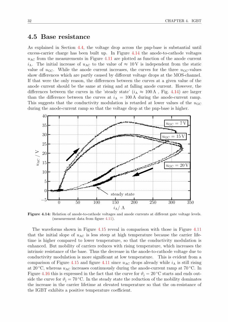
32 CHAPTER 4. IGBT
4.5 Base resistance
As explained in Section 4.4, the voltage drop across the pnp-base is substantial untilexcess-carrier charge has been built up. In Figure 4.14 the anode-to-cathode voltagesuAC from the measurements in Figure 4.11 are plotted as function of the anode currentiA. The initial increase of uAC to the value of ≈ 10 V is independent from the staticvalue of uGC. While the anode current increases, the curves for the three uGC-valuesshow differences which are partly caused by different voltage drops at the MOS-channel.If that were the only reason, the differences between the curves at a given value of theanode current should be the same at rising and at falling anode current. However, thedifferences between the curves in the ’steady state’ (iA ≈ 100 A , Fig. 4.14) are largerthan the difference between the curves at iA = 100 A during the anode-current ramp.This suggests that the conductivity modulation is retarded at lower values of the uGC
during the anode-current ramp so that the voltage drop at the pnp-base is higher.
uGC = 20 V
uGC = 15 V
uGC = 7 V
steady state
iA/ A
uA
C/
V
350300250200150100500
40
35
30
25
20
15
10
5
0
−5
Figure 4.14: Relation of anode-to-cathode voltages and anode currents at different gate voltage levels.(measurement data from figure 4.11).
The waveforms shown in Figure 4.15 reveal in comparison with those in Figure 4.11that the initial slope of uAC is less steep at high temperature because the carrier life-time is higher compared to lower temperature, so that the conductivity modulation isenhanced. But mobility of carriers reduces with rising temperature, which increases theintrinsic resistance of the base. Thus the decrease in the anode-to-cathode voltage due toconductivity modulation is more significant at low temperature. This is evident from acomparison of Figure 4.15 and figure 4.11 since uAC drops already while iA is still risingat 20 C, whereas uAC increases continuously during the anode-current ramp at 70 C. InFigure 4.16 this is expressed in the fact that the curve for ϑj = 20 C starts and ends out-side the curve for ϑj = 70 C. In the steady state the reduction of the mobility dominatesthe increase in the carrier lifetime at elevated temperature so that the on-resistance ofthe IGBT exhibits a positive temperature coefficient.

4.5. BASE RESISTANCE 33
uGC = 15 V
gate-to-cathode voltage uGC
anode-to-cathode voltage uAC
anode current iA/10
t/µs181614121086420
35
30
25
20
15
10
5
0
Figure 4.15: Current pulse through an IGBT with 15V permanent positive gate bias at junction tem-perature ϑj =70 C for comparison with figure 4.11.
ϑj = 20 C
ϑj = 70 C
iA/ A
uA
C/
V
350300250200150100500
35
30
25
20
15
10
5
0
Figure 4.16: Comparison of relations of anode-to-cathode voltages and anode currents at different junc-tion temperatures (measurement data from Figure 4.11 and Figure 4.15).
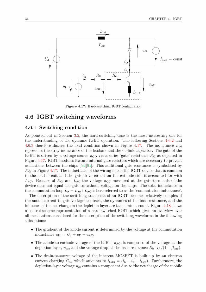
34 CHAPTER 4. IGBT
PSfrag replacements
anodecathode
gate
iA
uACuGC
Ud
uD
Lσ0
Iload = const
iA
iD
iG RG RGi
Lσ0
LσC
uGD
Figure 4.17: Hard-switching IGBT configuration
4.6 IGBT switching waveforms
4.6.1 Switching condition
As pointed out in Section 3.2, the hard-switching case is the most interesting one forthe understanding of the dynamic IGBT operation. The following Sections 4.6.2 and4.6.3 therefore discuss the load condition shown in Figure 4.17. The inductance Lσ0
represents the stray inductance of the busbars and the dc-link capacitor. The gate of theIGBT is driven by a voltage source uGD via a series ’gate’ resistance RG as depicted inFigure 4.17. IGBT modules feature internal gate resistors which are necessary to preventoscillations between the chips [54][91]. This additional gate resistance is symbolised byRGi in Figure 4.17. The inductance of the wiring inside the IGBT device that is commonto the load circuit and the gate-drive circuit on the cathode side is accounted for withLσC. Because of RGi and LσC the voltage uGC measured at the gate terminals of thedevice does not equal the gate-to-cathode voltage on the chips. The total inductance inthe commutation loop Lσ = Lσ0+LσC is here referred to as the ’commutation inductance’.
The description of the switching transients of an IGBT becomes relatively complex ifthe anode-current to gate-voltage feedback, the dynamics of the base resistance, and theinfluence of the net charge in the depletion layer are taken into account. Figure 4.18 showsa control-scheme representation of a hard-switched IGBT which gives an overview overall mechanisms considered for the description of the switching waveforms in the followingsubsections:
• The gradient of the anode current is determined by the voltage at the commutationinductance uLσ = Ud + uD − uAC.
• The anode-to-cathode voltage of the IGBT, uAC, is composed of the voltage at thedepletion layer, uds, and the voltage drop at the base resistance Rb · iA/(1 + βpnp).
• The drain-to-source voltage of the inherent MOSFET is built up by an electroncurrent charging Cdsj which amounts to iCdsj = (ib − id + iCgd). Furthermore, thedepletion-layer voltage uds contains a component due to the net charge of the mobile

4.6. IGBT SWITCHING WAVEFORMS 35
carriers that are traversing the depletion layer and add to the background-dopingconcentration . The portion of uds caused by this effect is considered by the factorkdepl that is multiplied by the difference of the hole current ic = iA · βpnp/(1 + βpnp)and the electron current id. The value of kdepl is proportional to the depletion-layerwidth.
• The MOSFET inherent in the structure of the IGBT is represented by its transcon-ductance gm = did/dugs which depends on the operation point (uds).
• The anode-current to gate-voltage feedback acts like an additional gate current forthe inherent MOSFET that is generated if the anode current changes. This effect isrepresented by the factor kfb that is multiplied by the gradient of the anode currentdiA/dt which yields a current that adds to the gate current. The factor kfb dependson the value of the gate-to-cathode voltage (Fig. 4.12).
• The current charging the gate-source capacitance Cgs is the gate current iG plus thevirtual gate current due to the anode-current to gate-voltage feedback minus thecurrent of Cgd.
• The (external) gate current of the device is given by the voltage at the total gateresistance. The stray inductance in the gate circuit is neglected here for clarity.
• The ’redistribution’ capacitance Ccer, which is only existent during turn-off, is ac-counted for by the factor kCcer which acts on the current gain of the inherent pnp-transistor. The effect represented by Ccer is that the relation of electron currentand hole current at the collector edge of the undepleted pnp-base is influenced bya changing width of the undepleted base. During typical IGBT anode-to-cathodevoltage transitions, the boundary of the undepleted, quasi-neutral base moves fasterthan with the base transit speed of the excess carriers [41]. Thus the excess-carrierdistribution cannot react to the moving boundary condition in a quasi-static wayanymore. This redistributes the excess carriers in the remaining undepleted partof the base, which leads to an additional hole-current component in the undepletedbase zone for two reasons: At first, additional holes are ’collected’ by the movingboundary of the space-charge region. Secondly, the narrowing of the undepletedbase increases the excess-carrier gradient from the emitter side to the collector sideof the pnp-base which also raises the hole-current [41]. Because the ’redistribution’current depends on the rate of change of the anode-to-cathode voltage, the effectcan be modelled with the redistribution capacitance Ccer, which is much larger thanCdsj. The factor kCcer acting on βpnp in Figure 4.18 is intended to illustrate themechanism more ’physically’. Of course a description explicitely accounting for theexcess-carrier charge would be more precise, but also much more complex.

36 CHAPTER 4. IGBT
+−
−
+
+
++
+−
−+
+++
+−+
−+
PSfr
agre
pla
cem
ents
1 Lσ
uA
C
ugs=
uG
C
Ud
uD
uLσ
i Adi A dt
kfb
uG
D
1R
G+
RG
i
i G
1C
gs
1C
gd
i Cgd
i Cgd
dugs
dt
g mi d
11+
βpnp
βpnp
1+
βpnp
βpnp
i c
i b
Rb
kdep
l
kC
cer
1C
dsj
duds
dt
uds
Figure 4.18: Control-scheme representation of a hard-switched IGBT

4.6. IGBT SWITCHING WAVEFORMS 37
4.6.2 Turn-on
Stages of turn-on
Figure 4.19 shows switching waveforms of a 3300 V/1200 A NPT IGBT (FZ1200R33KF1,Eupec) during turn-on with ϑj =20 C junction temperature. The commutation induc-tance Lσ amounts to Lσ = 110 nH. The turn-on process can be divided into three stages:
1. Delay phase
2. Current ramp
3. Voltage ramp.
Before turn-on (t < t0)
Prior to turn-on the IGBT blocks the dc-link voltage Ud and the freewheeling diode carriesthe load current Iload. The gate-to-cathode voltage equals the off-state gate-drive voltageUGD,off which amounts to constantly −9 V, so that the gate current
iG =1
RG + RG
· (uGD − uGC)
is zero.Considering the equivalent circuit in Figure 4.6 and Figure 4.18, the drain current of the
MOSFET and the collector current of the pnp-transistor are zero. The blocking voltageof the IGBT is supported by Cdsj which has a small value due to the depletion of thedrain at the junction J2. The gate-source capacitance Cgs is charged to UGD,off . Thenegative gate voltage induces an accumulation layer at the surface of the p-body regionand a depletion layer at the surface of the n+-gate-source overlap. The voltage of thegate-drain capacitance Cgd equals ugd = (ugs − uAC). As indicated before, Ccer is relatedto the removal of excess carriers during turn-off and has consequently not to be accountedfor in the discussion of the turn-on process.
Delay phase (t0 < tt1)
The time interval between the start of the turn-on process and the beginning of the currentramp is referred to as delay phase Td. To initiate the turn-on, the gate-drive voltage isswitched to UGD,on at time t0. Due to the voltage at the gate resistor a gate current
iG ≈ 1
RG + RGi
· (UGD,on − uGC) (LσC neglected)
is built up which charges Cgs. According to Kirchhoff’s voltage law a change of ugs
necessitates a change in the voltages of Cgd and Cdsj, which goes along with a displacementcurrent which is also provided by the gate driver. This displacement current changes thepotential of the semiconductor-oxide interface at the virtual MOSFET drain but does notafflict the anode-to-cathode voltage of the IGBT, since Cdsj and Cgd are associated withthe same depletion layer. This is an inaccuracy of the model shown in Figure 4.6. Whilethe inherent MOSFET is not conducting, the current of the gate-drain capacitance flowsthrough the cathode.

38 CHAPTER 4. IGBT
uAC/V (anode-to-cathode voltage)
iA/A (anode current)
t4t3t2t1t0
2000
1500
1000
500
0
-uD/V (diode voltage)
iD/A (diode current)
2000
1500
1000
500
0
-500
-1000
ugd/V (gate-drive voltage)
iG/A (gate current)
uGC/V (gate-to-cathode voltage)
t/µs20181614121086420
15
10
5
0
-5
-10
Figure 4.19: Turn-on of an NPT IGBT (FZ1200R33KF1, Eupec) under hard-switch conditions(RG,on = 4.7Ω, Ud = 2.2 kV, Iload = 1200A, ϑj = 20 C).
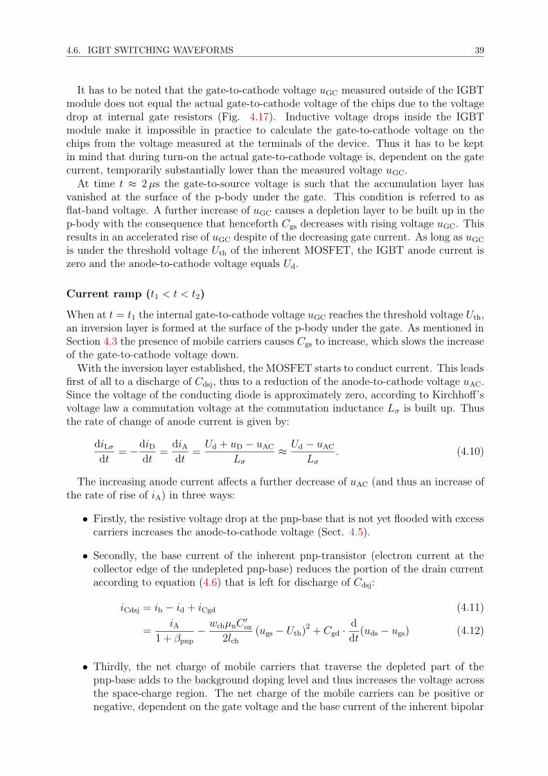
4.6. IGBT SWITCHING WAVEFORMS 39
It has to be noted that the gate-to-cathode voltage uGC measured outside of the IGBTmodule does not equal the actual gate-to-cathode voltage of the chips due to the voltagedrop at internal gate resistors (Fig. 4.17). Inductive voltage drops inside the IGBTmodule make it impossible in practice to calculate the gate-to-cathode voltage on thechips from the voltage measured at the terminals of the device. Thus it has to be keptin mind that during turn-on the actual gate-to-cathode voltage is, dependent on the gatecurrent, temporarily substantially lower than the measured voltage uGC.
At time t ≈ 2 µs the gate-to-source voltage is such that the accumulation layer hasvanished at the surface of the p-body under the gate. This condition is referred to asflat-band voltage. A further increase of uGC causes a depletion layer to be built up in thep-body with the consequence that henceforth Cgs decreases with rising voltage uGC. Thisresults in an accelerated rise of uGC despite of the decreasing gate current. As long as uGC
is under the threshold voltage Uth of the inherent MOSFET, the IGBT anode current iszero and the anode-to-cathode voltage equals Ud.
Current ramp (t1 < t < t2)
When at t = t1 the internal gate-to-cathode voltage uGC reaches the threshold voltage Uth,an inversion layer is formed at the surface of the p-body under the gate. As mentioned inSection 4.3 the presence of mobile carriers causes Cgs to increase, which slows the increaseof the gate-to-cathode voltage down.
With the inversion layer established, the MOSFET starts to conduct current. This leadsfirst of all to a discharge of Cdsj, thus to a reduction of the anode-to-cathode voltage uAC.Since the voltage of the conducting diode is approximately zero, according to Kirchhoff’svoltage law a commutation voltage at the commutation inductance Lσ is built up. Thusthe rate of change of anode current is given by:
diLσ
dt= −diD
dt=
diAdt
=Ud + uD − uAC
Lσ
≈ Ud − uAC
Lσ
. (4.10)
The increasing anode current affects a further decrease of uAC (and thus an increase ofthe rate of rise of iA) in three ways:
• Firstly, the resistive voltage drop at the pnp-base that is not yet flooded with excesscarriers increases the anode-to-cathode voltage (Sect. 4.5).
• Secondly, the base current of the inherent pnp-transistor (electron current at thecollector edge of the undepleted pnp-base) reduces the portion of the drain currentaccording to equation (4.6) that is left for discharge of Cdsj:
iCdsj = ib − id + iCgd (4.11)
=iA
1 + βpnp
− wchµnC′ox
2lch(ugs − Uth)
2 + Cgd ·d
dt(uds − ugs) (4.12)
• Thirdly, the net charge of mobile carriers that traverse the depleted part of thepnp-base adds to the background doping level and thus increases the voltage acrossthe space-charge region. The net charge of the mobile carriers can be positive ornegative, dependent on the gate voltage and the base current of the inherent bipolar

40 CHAPTER 4. IGBT
transistor. As depicted in Figure 4.18 this can be accounted for by writing the drain-to-source voltage of the inherent MOSFET as the sum of the depletion-layer voltageat zero current, and the difference of the hole current ic = iA · βpnp/(1 + βpnp) andthe electron current id multiplied by the resistance kdepl which is proportional to thedepletion layer width:
udsj =1
Cdsj
∫
iCdsj· dt + kdepl ·
(
iAβpnp
1 − βpnp
− id
)
(4.13)
The slope of the anode-to-cathode voltage uAC therefore is given by (Fig. 4.18)
duAC
dt=
1
Cdsj
(
iA1 + βpnp
− wchµnC′ox
2lch(ugs − Uth)
2 + Cgd ·d
dt(uds − ugs)
)
+d
dt
(
kdepl ·(
iAβpnp
1 − βpnp
− id
)
+ Rb ·iA
1 + βpnp
)
. (4.14)
It is understood that the values of all parameters in equation (4.14) are changing through-out the switching transient. The first bracket term on the right-hand side of equation(4.14) can be understood as a capacitive component of the output characteristic of theIGBT, while the following two terms represent a non-linear time-dependent resistive com-ponent. It is worth noting that the output capacitance is controlled by the gate-voltagelevel. As long as the value of the MOSFET drain current exceeds the value of the elec-tron current at the collector edge of the pnp-base, the output capacitance of the IGBTis virtually negative so that the anode-to-cathode voltage decreases at a positive anodecurrent. However, dependent on the gate-drive condition the anode-to-cathode voltage ofthe IGBT can rise again during the rise of the anode current when the retarding factorsin equation (4.14) exceed the accelerating terms.
The anode current of the IGBT also afflicts the gate voltage. As stated before, thevoltage drop across the MOSFET channel and at the drain surface reduces the localpotential difference between the gate electrode and the subjacent channel, which has beenreferred to as the anode-current to gate-voltage feedback in Section 4.4. The associateddisplacement current adds to the gate current provided by the gate driver which acceleratesthe rate of rise of uGC (fig. 4.18). This leads to the peak in the curve of the gate-to-cathode voltage in Figure 4.19. An increase in uGC however diminishes the voltage at thegate resistor, so that the magnitude of the gate current iG is reduced. Dependent on thegate-drive condition, the value of iG can even become slightly negative if the value of uGC
rises above the value of the gate-drive voltage during the rise of the anode current (whichdoes not occur in Figure 4.19). Thus, the anode-current to gate-voltage feedback causesa positive feedback during turn-on [34].
However, for the measurements in Figure 4.19 still another factor has to be considered:A part of the commutation voltage (Ud − uAC + uD) drops at the stray inductance LσC
inside the IGBT module which is common to load circuit and gate-drive circuit (Fig. 4.17).This voltage drop adds to the voltage measured at the gate terminals.
When the value of the anode current exceeds the value of the load current at t = t2, thecurrent of the freewheeling diode becomes negative. The reverse current iD = iA − Iload
builds up a space-charge region in the diode, thus a diode voltage uD appears. During

4.6. IGBT SWITCHING WAVEFORMS 41
this ’reverse recovery’ the diode can be regarded as a non-linear capacitor: The rate ofrise of the diode voltage is very low at the beginning of the slope because minority carriersstored in the drift region of the diode (’stored charge’) dynamically increase the outputcapacitance. The diode-voltage slope increases with rising voltage due to the non-linearcharacteristic of the space-charge capacitance (Cdepl ∼ u1/2) and due to the decay of theminority carriers by recombination. Meanwhile, the IGBT anode current continuous torise as long as uAC < Ud + uD holds, so that the voltage at Lσ is positive. When uD hasrisen to the value that (uAC + uD) > Ud at t = t3, iA starts to fall with the rate of falldetermined by the voltage at Lσ.
Voltage ramp (t3 < t < t4)
When the reverse current of the diode starts to decay for t > t3 due to the increasingdiode voltage, the falling IGBT anode-current iA accelerates the decay of uAC for thereasons explained above. At falling anode current the gate-to-cathode voltage decreasesdue to the anode-current to gate-voltage feedback and the voltage drop at LσC.
While the IGBT anode current declines after the reverse-recovery peak to the value ofthe load current Iload, an increasing share of the MOSFET’s drain current is available forthe discharge of Cdsj. However, a reduction of the drain-to-source voltage also requires adisplacement current through Cgd that is limited to
iG =UGD,on − uGC
RG + RGi
.
Consequently, the rate of fall of uAC can not exceed the value given by iG/Cgd. Otherwisethe current of Cgd would discharge Cgs which would reduce the gate-to-cathode voltage,thus the drain current. This in turn would decrease the gradient of the anode-to-cathodevoltage. That way a negative feedback exists for the gradient of the anode-to-cathodevoltage.
Cgd strongly increases at low drain-to-source voltages. That means that the negativefeedback for the gradient of uAC increases. In consequence the curve of uAC approaches thestatic on-state voltage quite slowly while the gate-to-source voltage is held approximatelyconstant, because the gate current is taken completely by Cgd. This is referred to as the’turn-on plateau’ of the gate voltage. It is worth pointing out that at constant anodecurrent the gate-to-cathode voltage determines the drain current, thus the slope of theanode-to-cathode voltage of the IGBT.
After the decay of uAC to a value near the steady-state value, the gate-source capac-itance Cgs is finally charged to UGD,on for t > t4, which further reduces the channelresistance and therefore uAC. Meanwhile, the operation point of the inherent MOSFETshifts into the non-saturation region of the static output characteristics.

42 CHAPTER 4. IGBT
4.6.3 Turn-off
Stages of turn-off
Figure 4.20 shows the switching waveforms of a 3300 V/1200 A NPT IGBT (FZ1200R33KF1,Eupec) during turn-off with ϑj = 20 C junction temperature. The turn-off process isagain divided into three stages:
1. Delay phase
2. Voltage ramp
3. Current ramp.
Before turn-off (t < t0)
In the on-state, the gate-drive voltage amounts to uGD = UGD,on = 16 V. The gate-sourcecapacitance Cgs of the inherent MOSFET is loaded to UGD,on so that the gate currentiG is zero. The inherent MOSFET operates in the non-saturation region of its outputcharacteristics (saturation region of the IGBT characteristics, Fig. 4.4) and provides thebase current for the pnp-transistor.
Cgs is large due to the channel-inversion layer and due to carrier enhancement under thegate-source overlap. Because the gate has a positive potential with respect to the MOS-FET’s drain (ugd = (ugs − uds) > 0), an accumulation layer exists at the semiconductor-oxide interface of the drain so that Cgd has a large value, too. Due to the small width ofthe space-charge region at J2, the capacitance of Cdsj is large.
According to the model in figure 4.6 and the control scheme in figure 4.18 the anode-to-cathode voltage equals the sum of the voltage drop along the conductivity-modulatedpnp-base (’drift region’) and the voltage of the base-collector depletion-layer capacitancewhich is identical with the MOSFET’s drain-to-source voltage:
uAC = uds + Rb · ib. (4.15)
The static on-state voltage depends on the anode current and the gate voltage. Comparedto the voltage at Cdsj, the voltage drop at the base resistance is negligible during the turn-off switching process since the undepleted base is in the high-level injection condition.
According to the inductive load the anode current iA is approximately constant beforeturn-off.
Turn-off delay (t0 − t2)
The turn-off process is initiated at t = t0 by switching the gate-drive voltage to UGD,off .According to the difference of the gate-drive voltage and the gate-to-cathode voltage, anegative current is built up in the gate resistor which discharges both Cgd and Cgs tosmaller absolute voltages. The displacement current of Cgd which adds to the electroncurrent at the collector edge of the pnp-base is negligible compared to the MOSFETdrain current. The drain-to-source voltage increases due to the decreasing gate-to-cathodevoltage. However, the impact on the drain current is relatively small, since id increaseswith uds as long as the inherent MOSFET is operating in the ohmic region of its outputcharacteristics.

4.6. IGBT SWITCHING WAVEFORMS 43
iA/A (anode current)
uAC/V (anode-to-cathode voltage)
t4t3t2t1t03000
2500
2000
1500
1000
500
0
-uD/V (diode voltage)
iD/A (diode current)
2000
1500
1000
500
0
uGD/V (gate-drive voltage)
iG/A (gate current)
uGC/V (gate-to-cathode voltage)
t/µs20181614121086420
15
10
5
0
-5
-10
Figure 4.20: Turn-off of an NPT IGBT (FZ1200R33KF1, Eupec) under hard-switch conditions(RG,off = 6.2Ω, Ud = 2.2 kV, Iload = 1200A, ϑj = 20 C).

44 CHAPTER 4. IGBT
When the MOS channel is pinched off at t = t1 because of the decreasing gate-to-cathode voltage, the operation point of the MOSFET shifts into the saturation regionand the drain current becomes independent from uds. This is expressed by the smallslope of the characteristic curves in the ’active region’ (Fig. 4.4). A further decrease ofthe gate-to-source voltage now reduces the drain current (eqn. (4.5)). With the totalcurrent in the pnp-base being constant during this phase because of the inductive load,and with the transport of electrons and holes in the pnp-base being coupled due to thehigh-level injection condition, the reduction of id causes a lack of electron current atthe collector edge of the undepleted base. The lacking electron current is replaced byreduction of the local electron concentration which widens the depletion layer at thejunction J2. In reference to figures 4.6 and 4.18 it is the difference of the electron basecurrent ib = iA/(1 + βpnp) required for the total carrier transport in the base and theelectron current injected into the base by the MOSFET’s drain and through Cgd, whichcharges Cdsj and which therefore is responsible for the rate of rise of uds:
duds
dt=
1
Cdsj
(
ib − id + iCgd
)
(4.16)
=1
Cdsj
(
iA1 + βpnp
− id + Cgd ·d
dt(ugs − uds)
)
(4.17)
The drain current, thus the gate-to-cathode voltage of the IGBT, determines the part ofthe base current that charges Cdsj. Hence the output capacitance of the IGBT duringturn-off is controlled by the gate-to-cathode voltage level.
At low anode-to-cathode voltage there is no depletion layer under the oxide-drain in-terface, so that Cgd equals Coxd which has a large and approximately constant value. Therising anode-to-cathode voltage is linked with a displacement current through Cgd whichhas to be supplied by the gate drive circuit and which reduces the current dischargingCgs. Hence the rate of rise of uAC is limited to
duAC
dt≤ − 1
Cgd
· iG =1
Cgd
· uGC − UGD,off
RG
. (4.18)
When equality in equation (4.18) is fulfilled, the gate current is taken completely by Cgd
which prevents a further decrease of uGC, thus a reduction of id which determines the slopeof uAC. The negative feedback via Cgd leads to the so-called turn-off plateau (t1 < t < t2)in the gate-to-cathode voltage.
The contribution of the charge of mobile carriers to the depletion layer voltage is neg-ligible during this phase because of the small depletion-layer width. The rate of rise ofthe anode-to-cathode voltage during the turn-off plateau is very low since Cdsj is largeand Cgd is large as well, causing a strong negative feedback. This is the reason why theplateau phase is assigned to the turn-off delay, though uAC is actually rising already.
Voltage ramp (t2 < t < t3)
When uAC exceeds uGC at t = t2, a depletion layer forms at the oxide-drain interface andthe capacitance of Cgd decreases significantly. The reduction in the displacement currentthrough Cgd gives way to a decrease of uGC which reduces the output admittance of theIGBT by decreasing the drain current. With the anode current iA still being constant this

4.6. IGBT SWITCHING WAVEFORMS 45
accelerates the rate of rise of the anode-to-cathode voltage uAC. The negative feedbackthrough Cgd persists as long as the rate of rise of the anode-to-cathode voltage at zerodrain current exceeds the quotient of the gate current iG and gate-drain-capacitance Cgd.Otherwise the slope of the anode-to-cathode voltage is only determined by the outputcapacitance of the IGBT and the anode current.
Dependent on the value of the IGBT’s anode current, two cases can be distinguishedwith respect to the curves of the gate-to-cathode voltage during turn-off: Either, the rateof rise of uAC is limited by the electron current at the collector edge of the undepletedbase and the drain-source capacitance. Then the gate is continously discharged duringthe rise of the anode-to-cathode voltage and the MOSFET is turned off completely in anearly stage of the turn-off process. Or the slope of the anode-to-cathode voltage is limitedby the ratio Cgd/iG and the MOSFET stays active, reducing the slope of uAC with itsdrain current. The latter is the case for the measurements shown in Figure 4.20, the firstwill be encountered with so called ’field-stop’ devices (Chapter 7).
As stated in Subsection 4.6.1, the moving boundary of the depletion layer at the base-collector junction during the uAC-ramp causes an increase of the hole-current at the col-lector edge of the undepleted base. Consequently the current ib in Figure 4.6 and figure4.18 is reduced, which decreases the current charging Cdsj. For that reason Cdsj appearsto be largely increased during the uAC-ramp at turn-off due to the excess-carrier charge.In [40] this has been accounted for by the ’redistribution’ capacitance Ccer (fig. 4.6).
For high anode-to-cathode voltages, the net charge of the mobile carriers which traversethe depleted part of the base becomes relevant [38]). This effect plays a much bigger roleduring turn-off than during turn-on, because the hole current portion of the total currentis increased due to the withdrawal of the MOSFET drain current.
Current ramp (t3 < t < t4)
When the IGBT’s anode-to-cathode voltage exceeds the dc-link voltage at t = t3, thefreewheeling diode becomes forward-biased. To commutate the current from the IGBTto the diode, a commutation voltage at the commutation inductance Lσ = Lσ0 + LσC
is needed which has to be provided by the IGBT. The uAC overvoltage required for thecommutation is increased by the forward-recovery voltage of the diode. With the rate ofchange of the anode current given by (Ud − uAC + uD)/Lσ, the anode-to-cathode voltageuAC of the IGBT continues to rise as long as a share of the base current (electron currentat the collector edge of the undepleted base) is charging Cdsj. The increase of uAC isaccelerated by the net charge of the mobile carriers in the depletion region which ispositive due to the withdrawal of the drain current.
When the current starts to commutate to the diode, the sinking anode current of theIGBT reduces the electron current at the collector edge of the pnp-base which is chargingthe depletion layer capacitance und which thus is responsible for the rise of the anode-to-cathode voltage. Furthermore, the decrease of the total current also diminishes theconcentration of the mobile holes in the depleted base-collector junction which reducesthe voltage at the depletion layer. Together, this leads to a progressive reduction of theanode-voltage slope after the onset of the anode-current fall, so that after a while uAC
ceases to increase and then starts to fall. The gradient of uAC is zero when the increaseof the depletion layer voltage due to the lack of electron current on the base side balancesthe decrease due to the vanishing charge of mobile holes. In the following the decrease

46 CHAPTER 4. IGBT
of uAC due to the vanishing concentration of mobile holes in the depleted base dominatesthe further growth of the depletion layer width caused by the electron portion of theremaining base current. The reason is that the output capacitance is still large due toexcess-carrier charge stored in the undepleted pnp-base, meaning that the hole-currentcomponent at the collector edge of the base is large. So, the ’capability’ of the remaininganode current to increase uAC is low. Thus the anode-to-cathode voltage decreases to thevalue of the dc-link voltage, despite of the remaining anode current.
The falling anode-to-cathode voltage causes a steady decrease of the commutation volt-age, thus a decrease of the anode-current slope. In consequence the anode current decaysvery slowly. The slow decay of iA is referred to as ’anode-current tail’. This ’tail current’is usually explained simply with the sweeping out of the excess carriers. However, theanode current is only indirectly linked to the stored charge, since the anode current isgiven by the time integral of the commutation voltage which depends upon the anodevoltage of the IGBT.
With the change of sign of the gradient of uAC, the direction of the current in Cgd isinverted, too, which leads to an accelerated fall of the gate-to-cathode voltage after thepeak of uAC. The anode-current to gate-voltage feedback further speeds up the decay ofuGC. Because of the stray inductance in the cathode path of the IGBT common to loadcircuit and gate-drive circuit, a part of the dynamic of uGC is due to the decay of theanode current, or to be more precisely — due to the share of commutation voltage at theinternal stray inductance of the IGBT device.
4.7 Latch-Up
Apart from the MOSFET and the pnp-transistor, a parasitic npn-transistor is containedin the structure of the IGBT. It is formed by the n+-MOSFET source, the subjacent p-body region, and the pnp-base as shown in figure 4.21. To keep control over the gate it isessential that the thyristor structure formed by the npn-transistor and the pnp-transistordoes not latch in such a way, that the npn-transistor provides the electron base current forthe pnp-transistor. The npn-transistor is turned on, if its base-to-emitter voltage is highenough that electron injection from the n+-drain into the p-body / npn-base occurs. Thiscan happen because of the lateral voltage drop in the p-doped cathode (pnp-collector)region, though base and emitter are actually shorted by the cathode metallization. Theresistivity of the p-body is indicated by the ’shunting’ resistor RS in Figure 4.21. Tomaximise the anode-current level before latch-up, the resistance of the p-body under thecathode is minimized by means of a higher doping level in the center of the p-body [7][99]as indicated in figure 4.1.
In addition, the current density and thus the voltage drop has to be kept within certainlimits. This can be done by appropriate shaping of the cells [8][124] and by loweringthe current gain βpnp of the pnp-transistor and therefore the hole injection into the pnp-collector region. Since βpnp increases with temperature due to increased carrier lifetime[18][127], the critical current density in the p-body is already reached at a lower anodecurrent level at elevated temperature.
Apart from the ’static latch-up’ which occurs when the anode current exceeds a criticalvalue in the on-state, a ’dynamic latch-up’ can occur during turn-off with clamped induc-tive load at current levels lower than the static latching current. The reason is that the

4.7. LATCH-UP 47
PSfrag replacements
Anode
CathodeGate
g
d s
b
b
e
e
c
c
Ugs
p+
p
n+
n−
RS
iC
J1
J2
J3
Figure 4.21: Equivalent circuit of the IGBT, latching structure.
inductive load keeps the anode current constant during the voltage rise. As the MOSFETelectron current in the pnp-base is reduced during turn-off, the lacking electron currentmust be substituted by an increased hole current which raises the voltage drop at thep-body resistance RS and thus can lead to a latch-up [125]. In addition, the MOS-channelvoltage which is at the same time the base-to-collector voltage of the npn-transistor risesduring turn off, which reduces the neutral base width of the pnp-transistor and thusincreases the current gain. Consequently the injection of electrons into the pnp-base isincreased.
A dynamic latch-up can also be triggered by a dynamic avalanche generation duringturn-off [82]. The holes generated by avalanche multiplication in the space-charge regionare swept into the p-body / pnp-collector of the IGBT structure. If the voltage drop inthe p-body exceeds the built-in potential of the body-source junction, the base-emitterdiode of the inherent npn-transistor becomes forward-biased. In consequence, electronsare injected into the p-body and collected by the space-charge region at the n-base –p-body junction. When the value of this electron current reaches the value of the electroncurrent at the collector edge of the pnp-base, the IGBT latches.
Figure 4.22 shows switching waveforms of a turn-off failure with dynamic latch-up. Theanode-to-cathode voltage uAC increases to the value of 3000 V. Then uAC breaks downbecause the npn-transistor inherent in the structure of the IGBT is turned on by thevoltage drop in the p-body. The collector current of the pnp-transistor rapidly dischargesthe space-charge capacitance at the junction J2 which leads to a sudden decrease of theanode-to-cathode voltage of the IGBT. This at first makes the commutation voltage atthe stray inductance zero, so that the anode current iA ceases to fall. When uAC decaysfurther, the voltage at the stray inductance is inverted so that the anode current startsto rise rapidly. When the value of iA exceeds the value of the load current, the diode iscommutated very fast. Since few excess-carrier charge is present in the diode due to theshort conduction time, the output capacitance is small. This leads to a sharp increaseof the diode voltage, which results in a destructive overvoltage because of the extremereverse current. Thus the diode voltage collapses after a short peak. After the breakdownof the diode, the voltages measured at the device is the sum of the inductive voltage drops

48 CHAPTER 4. IGBT
at the internal wiring and the voltage over the arcs inside the devices. The voltage ofthe IGBT after the breakdown is substantially higher. Apparently the IGBT is not yetdestroyed and operates in the thyristor mode, with extremely high anode current.
4.8 Short circuit
If the load is short-circuited while the IGBT is statically in the on-state, the anodecurrent of the IGBT increases rapidly; the rate of rise of iA is determined by the voltageat the commutation inductance (eqn. (4.10)). It is assumed here that the gate-to-cathodevoltage is constant. The increase in the anode current is accompanied by an increase ofthe electron current in the pnp-base, which is the base current of the pnp-transistor inFigure 4.6. As long as the inherent MOSFET is operating in the nonsaturation regionof its static output characteristics (’saturation region’ of the IGBT characteristics, Fig.4.4), this causes a moderate increase of both the drain current and the drain-to-sourcevoltage.
When the drain current has reached the value that the MOS-channel is pinched off dueto the lateral voltage drop at the inversion layer, the increase of the drain-to-source voltagedoes no longer result in a growing the drain current. The lack of electron current at thecollector edge of the undepleted pnp-base widens the space-charge region which enlargesthe anode-to-cathode voltage. This is referred to as ’desaturation’. With reference tofigure 4.6 the difference of drain current and displacement current through Cgd on the onehand, and the base current on the other hand charges the depletion-layer capacitance Cdsj;consequently, the drain-to-source voltage increases rapidly. If uAC reaches the value of thedc-link voltage, the voltage at Lσ becomes zero which prevents a further increase of theshort-circuit current. Dependent on the output characteristics of the IGBT the anode-to-cathode voltage can rise above the dc-link voltage. This reduces the anode current dueto the negative voltage at the commutation inductance. In consequence, uAC decreasesdue to the reduced ohmic voltage drop and possibly because of the reduced net charge ofmobile carriers in the space-charge region at the collector-base junction (Fig. 4.5). Henceboth anode-to-cathode voltage and anode current can show an overshoot before they reachtheir static values.
The limitation of short-circuit currents is one of the major advantages of the IGBTover thyristor-type semiconductor switches. This ability is owing to the fact that nopositive internal feedback exists that provides base current for the inherent pnp-transistor.However, this is not absolutely true because of the existing anode-current to gate-voltagefeedback (Section 4.6.3) and due to the gate-drain ’feedback’ capacitance Cgd (Fig. 4.6).Especialy at low uAC levels when Cgd is large, the current through Cgd due to the risinganode-to-cathode voltage is substantial. If this displacement current is not drained offthrough the gate drive, it raises the gate-to-cathode voltage and thus the MOSFET draincurrent. To limit short-circuit currents effectively it is thus essential to avoid an increaseof the gate-to-cathode voltage above the static value, e.g. by clamping.
If the load is already shorted when the IGBT is turned on, the anode-to-cathode voltageat first decreases slighly since the inherent MOSFET discharges the space-charge capac-itance Cdsj (Fig. 4.6). This causes a voltage at the inductance of the short-circuit meshwhich gives rise to an increasing anode current. Like in case of a conventional turn-on,the base current ib of the inherent pnp-transistor reduces the current that is discharging

4.8. SHORT CIRCUIT 49
anode-to-cahtode voltage vAC / Vanode current iA / A
3000
2500
2000
1500
1000
500
0
diode voltage uD/ V
500
0
−500
−1000
−1500
−2000
−2500
gate current iG/ A
gate-to-cathode voltage uGC/ V
t/µs10987654321
15
10
5
0
−5
−10
Figure 4.22: Dynamic latch-up of a FZ1200R33KL2 ENG IGBT (Eupec) (Ud = 2200V, Iload = 1770A,ϑj = 120C, RG,off = 2Ω).

50 CHAPTER 4. IGBT
Cdsj which prevents a further decay of the anode-to-cathode voltage. When ib exceeds thedrain current, the anode-to-cathode voltage uAC increases again. The anode current con-tinues to rise, until the voltage at the stray inductance of the short-circuit mesh becomezero due to the increase of uAC. The anode-to-cathode voltage rises as long as the basecurrent of the inherent pnp-transistor exceeds the drain current of the inherent MOSFET.
A turn-on under short-circuit condition is less difficult to handle than a short thatoccurs when the IGBT is already turned on [30][29]. The reason is that the feedbackthrough the gate-drain capacitance lacks due to the approximately constant anode-to-cathode voltage. In addition, the pnp-base is not yet flooded with excess carriers so thatthe anode-to-cathode voltage rises faster.
4.9 IGBT gate-drive requirements
4.9.1 Static off-state
When the IGBT is in the off-state, the gate drive has to prevent an unintended turn-on. The latter can occur due to the gate-drain ’feedback’ capacitance Cgd (Fig. 4.6) ifthe anode-to-cathode voltage rises rapidly, for example during the commutation of theantiparallel diode in a voltage-source converter. The displacement current through Cgd
charges the gate-source capacitance Cgs, if the current is not drained through the gatecontact. Hence the connection between the gate drive and the IGBT device must havea sufficiently low impedance to prevent an unintended turn-on. Since zero impedance inthe gate-drive circuit is not feasible, the static gate-to-cathode voltage of the IGBT in theoff-state has to be considerably lower than the gate-threshold voltage. This is to preventthat the inevitable current through Cgs due to the impedance in the gate circuit leads toa turn-on. Thus the required negative gate bias in the off-state depends on the magnitudeof Cgd, the maximal slope of the anode-to-cathode voltage and the impedance in the gatecircuit.
A capacitor connected between gate and cathode terminal of the IGBT device im-proves the ruggedness against unintended turn-on. With the gate-source capacitance thusincreased, a greater amount of charge is necessary to raise the gate-to-cathode voltageabove the threshold level.
4.9.2 Static on-state
For a low on-state voltage, the level of the gate-to-cathode voltage has to be high enoughto move the point of operation in the static output characteristics (fig. 4.4) as far aspossible to the left. However, a high gate bias in the on-state also results in a large short-circuit current in case of a failure. Hence the choice of the static gate-to-cathode voltagein the on-state is a trade-off between low on-state losses and high ruggedness againstshort-circuit situations.
Without any measures taken, the gate-to-cathode voltage rises during a short-circuitsituation. This is due to the anode-current to gate-voltage feedback and due to thefeedback through the gate-drain capacitance Cgd. To limit the short-circuit current, thegate drive thus has to keep the gate-to-cathode voltage as constant as possible.
A short can be detected by monitoring the anode-to-cathode voltage of the IGBT. If ashort is detected, the IGBT has to be turned off within several microseconds, to prevent

4.10. TURN-OFF 51
thermal destruction of the device. Since the value of the anode current under short-circuitcondition is much higher than the nominal anode current, the IGBT is jeopardised due toexcessive overvoltage and due to dynamic latch-up while shutting down the short-circuitcurrent. Hence the IGBT must be turned off slowly if a short has been detected [30].
4.9.3 Turn-on
As far as the IGBT is concerned, the turn-on process should be as fast as possible, to min-imise turn-on switching losses. However, in case of a clamped inductive load (fig. 4.17),the reverse recovery of the freewheeling diode is strongly affected by the turn-on waveformof the anode-to-cathode voltage of the IGBT.
As long as the anode current of the IGBT is below the load-current level so that thediode current is positive, the rate of rise of iA should be as high as possible to minimiselosses ([t1 < t < t2], Fig. 4.19). That means that the anode-to-cathode voltage shouldbe low so that the voltage at the commutation inductance is high (eqn. 3.8).
When iA exceeds the load current, the direction of the diode current is inverted. Theslope of the anode current during the extraction of the stored charge of the diode deter-mines the level of the reverse current at which the diode voltage starts to rise after thestorage phase (Fig. 3.9, Fig. 4.19). The value of the reverse current determines boththe rate of rise of the diode voltage and the peak power dissipation of the diode. Hencethe reverse current of the diode has to be limited to prevent destruction due to dynamicavalanche [24] on the one side and to avoid excessive overvoltage on the other side. Con-sequently, during the ’storage phase’ of the diode the minimal admissible value of theanode-to-cathode voltage of the IGBT is dictated by the maximal allowable slope of thereverse current of the diode.
As soon as the diode starts to support a blocking voltage ([t3 < t < t4], Fig. 4.19),the diode voltage adds to the voltage at the commutation inductance (eqn. 3.8). Thediode voltage is determined by the time integral of the reverse current and the differentialoutput capacitance of the diode. If the anode-to-cathode voltage of the IGBT remainshigh, the reverse current is quickly reduced. But, the slope of the diode voltage is low.If the anode-to-cathode voltage of the IGBT however decays rapidly, the reverse currentremains high which results in a steep increase of the diode voltage. This also causes ahigh peak power dissipation of the diode since the voltage is built up with a large current.
4.10 Turn-off
During the turn-off process, the gate drive has to limit the slope of the anode-to-cathodevoltage for two reasons. Firstly, the slope of uAC has to stay within certain limits to avoidthe dynamic latch-up of the IGBT (Section 4.7). A dynamic latch-up occurs due to anexcessive collector (hole) current of the inherent pnp-transistor which is caused by thewithdrawal of the MOSFET drain current and by the moving depletion-layer boundary inthe pnp-base (Section 4.6.3). Secondly, the slope of the anode-to-cathode voltage has to belimited to reduce both voltage spikes on the electric lines to the load, and electromagneticinterferences with other components.
Furthermore, it is desirable that the gate drive limits the maximum anode-to-cathodevoltage during the commutation to a distinct value to prevent destructive overvoltages

52 CHAPTER 4. IGBT
which is referred to as ’active clamping’. If this is not feasible, the slope of the anode-to-cathode voltage has to be limited such that the anode current is commutated before themaximum anode-to-cathode voltage is exceeded.
As seen in Section 4.6.3, the slope of the anode-to-cathode voltage during turn-offcan only be limited, but not totally be controlled by the gate drive. Especially at lowload current the gradient of the anode-to-cathode voltage is low, even if the inherentMOSFET is turned off completely becauses the current charging the output capacitanceis low. However, as long as the value of the gate-to-cathode voltage is above the thresholdlevel, the slope of the anode-to-cathode voltage can be reduced by acting on the gate.

53
5 IGBT design
5.1 P-Channel IGBT
Apart from the n-channel IGBT (with the inherent MOSFET being of the n-channel type)also p-channel IGBTs have been investigated [16][100]. The structure of a p-channel IGBTis identical with that of a n-channel IGBT, with the doping type of each semiconductorregion inverted.
Compared to its n-channel counterpart, the p-channel IGBT is characterized by thelower mobility of holes and higher carrier lifetime in the p-base of the inherent wide-basebipolar transistor. The latter leads to a higher gain of the wide-base transistor whichmakes the devices even more susceptible to latch-up. The lower hole mobility has noeffect if the current gain of the wide-base transistor is high and therefore the portion ofhole current is low. However, at practical current gains which are small for the benefitof reduced switching losses, the lower mobility of holes leads to forward voltages thatare higher than those of a n-channel IGBT with comparable switching characteristics. Afurther disadvantage is that the passivation of a p−-silicon surface is more difficult. Forthese reasons the development of the IGBT has been focused on the n-channel type.
5.2 Switching speed enhancement
The IGBT turns off relatively slowly because of the great amount of excess carriers storedin the base of the inherent pnp-transistor. The stored charge enlarges the output capaci-tance as discussed in Section 4.6.3.
To increase the switching speed, the charge stored in the pnp-base in the on state mustbe decreased. This can be done either by reduction of the total pnp-base volume orby reduction of the excess-carrier concentration. However, a gain in switching speed isnecessarily bought by increased on-state losses because of the reduced carrier density inthe low-doped pnp-base.
Methods to increase switching speed are [37]:
1. Reducing the excess-carrier lifetime
2. Limiting the injection efficiency of the p-emitter
3. Employing a buffer layer structure as known from the power diode.
These methods are outlined in the following Sections 5.3– 5.9 together with other designaspects.

54 CHAPTER 5. IGBT DESIGN
5.3 Lifetime control
At a given emitter efficiency the density of the excess carriers in the pnp-base can belowered by introduction of recombination centres to reduce the carrier lifetime. Methodsto achieve this can be divided into [3][5]
1. the thermal diffusion of impurities (gold, platinum) that exhibit deep levels in theenergy gap of silicon and
2. the creation of lattice damages by irradiation with high-energy particles includingelectrons, protons, neutrons, and α-particles.
Regions of reduced carrier lifetime introduced by metal-diffusion methods stretch acrossthe entire wafer thickness while the lateral extent can be controlled with 100 µm accuracy[101][19].
Electron irradiation degrades the carrier lifetime in the entire volume of the device. Thistechnique was one of the first applied to IGBTs because it was well established in theproduction of p-i-n rectifiers [1][6]. Compared to metal diffusion, electron irradiation offersgreater precision with respect to the recombination-centre concentration, which results ina lower spread in the device characteristics [5]. Neutron irradiation was suggested becauseof the expectation that the effect of lattice defects introduced by fast neutrons was superiorto those achieved with electron irradiation. However, the nature of crystal defects turnedout to be the same for both technologies [35] [107]. In contrast to electron irradiation,proton irradiation allows a vertical localization of recombination centres [75][32]. Aneven better vertical localization of the afflicted region can be achieved when helium orα-particle implantation is used [101]. Because of difficulties in masking proton, α, orhelium irradiation the control of the lateral extension of the irradiated region is limitedto an accuracy of ≈ 100 µm.
Since the trade-off between switching speed and on-state voltage is improved withconfined regions of reduced carrier lifetime [110], manufacturers recently prefer meth-ods allowing a localized introduction of recombination centres despite of the higher cost[75][32][50][77][120].
5.4 Emitter efficiency
The straightforward way to decrease the excess-carrier density in the on-state is to lowerthe emitter efficiency γe (eqn. (4.1)) of the p+-anode region. Because of continuity,the emitter efficiency is determined by the gradient of the electron concentration in theemitter where the transport of electrons is due to diffusion. Thus the emitter efficiencydecreases with decreasing doping concentration of the emitter. If the doping of the anoderegion is high for technological reasons, a n-doped buffer layer between the emitter andthe low-doped pnp-base can be used to reduce the emitter efficiency [80][42].
5.5 Punch-through IGBT
If the depletion layer in an IGBT with buffer layer extends through the whole low-dopedpnp-base (’punch-through’), the electric field takes a trapezoidal shape with a further
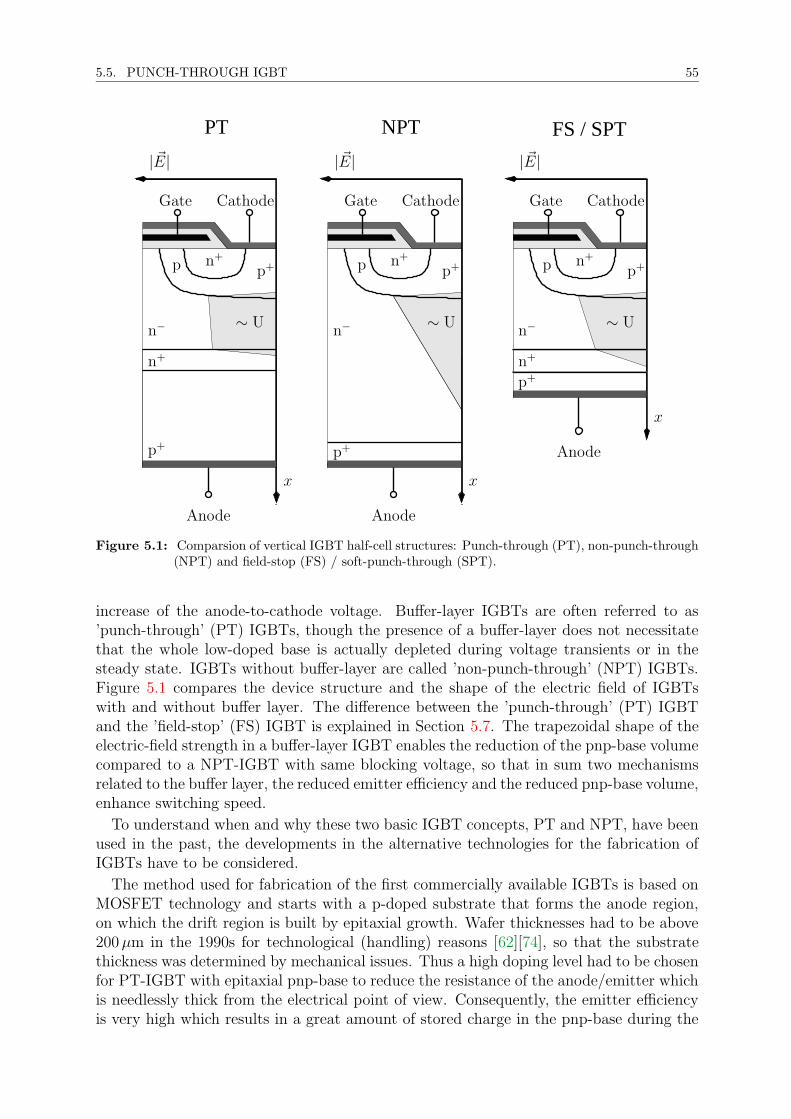
5.5. PUNCH-THROUGH IGBT 55
NPTPT FS / SPT
PSfrag replacements
| ~E|| ~E|| ~E|
n+ n+
n+ n+n+
n− n−n−
p pp
p+
p+
p+
p+ p+p+
CathodeCathodeCathode
Anode Anode
Anode
GateGateGate
∼ U ∼ U ∼ U
x
xx
Figure 5.1: Comparsion of vertical IGBT half-cell structures: Punch-through (PT), non-punch-through(NPT) and field-stop (FS) / soft-punch-through (SPT).
increase of the anode-to-cathode voltage. Buffer-layer IGBTs are often referred to as’punch-through’ (PT) IGBTs, though the presence of a buffer-layer does not necessitatethat the whole low-doped base is actually depleted during voltage transients or in thesteady state. IGBTs without buffer-layer are called ’non-punch-through’ (NPT) IGBTs.Figure 5.1 compares the device structure and the shape of the electric field of IGBTswith and without buffer layer. The difference between the ’punch-through’ (PT) IGBTand the ’field-stop’ (FS) IGBT is explained in Section 5.7. The trapezoidal shape of theelectric-field strength in a buffer-layer IGBT enables the reduction of the pnp-base volumecompared to a NPT-IGBT with same blocking voltage, so that in sum two mechanismsrelated to the buffer layer, the reduced emitter efficiency and the reduced pnp-base volume,enhance switching speed.
To understand when and why these two basic IGBT concepts, PT and NPT, have beenused in the past, the developments in the alternative technologies for the fabrication ofIGBTs have to be considered.
The method used for fabrication of the first commercially available IGBTs is based onMOSFET technology and starts with a p-doped substrate that forms the anode region,on which the drift region is built by epitaxial growth. Wafer thicknesses had to be above200 µm in the 1990s for technological (handling) reasons [62][74], so that the substratethickness was determined by mechanical issues. Thus a high doping level had to be chosenfor PT-IGBT with epitaxial pnp-base to reduce the resistance of the anode/emitter whichis needlessly thick from the electrical point of view. Consequently, the emitter efficiencyis very high which results in a great amount of stored charge in the pnp-base during the

56 CHAPTER 5. IGBT DESIGN
on-state and therefore in high turn-off losses. To obtain acceptable switching losses, theexcess-carrier concentration in the pnp-base has to be reduced. It was found that deviceswith a buffer layer, which degrades the emitter efficency and allows the reduction of thepnp-base volume, are superior to epitaxically built devices without buffer layer which areusing only lifetime control to reduce the excess-carrier densitiy [42][79]. For that reason,epitaxial fabrication and buffer-layer design have become idiomatic.
Due to difficulties growing thick epitaxial layers [4][50][71][79] and because of the highcost for epitaxial silicon, this technology initially was restricted to devices with lowerblocking voltages up to 1200 V. Despite the reduction of emitter efficiency obtained bythe buffer layer, the emitter efficiency is still high (γPT ≈ 1, [102]), so that a reduction ofcarrier lifetime is necessary for buffer-layer IGBTs built with epitaxy.
Due to carrier-lifetime control, the excess-carrier concentration in the low-doped base ofthe PT-IGBT has a strong gradient. Hence the hole current is predominantly a diffusioncurrent.
During turn-off of a PT IGBT, all stored charge is swept out of the low-doped base bythe electric field, which leads to a fast decay of the anode current. Thus PT-IGBTs showno anode-current ’tail’ at turn-off.
5.6 Non-punch-through IGBT
The second way to build an IGBT is to use a lightly n-doped (’float-zone’, ’bulk’) waferas starting material. Here the p-anode (pnp-emitter) is formed by implantation. Becauseof the earlier mentioned limitations concerning the minimum wafer thickness [62][74], thismethod was reserved to devices with blocking voltages of 1200 V and above in the earlydays of the IGBT [62]. It is not acceptable to have the low-doped pnp-base much widerthan necessary, because of its high resistivity. With the minimum wafer thickness beingrestricted, it was consequently not feasible to build PT-IGBTs which require an eventhinner drift zone with this technology.
In contrast to the epitaxial PT-IGBT with its thick and highly doped emitter, theemitter efficiency of the NPT-IGBT can be chosen very low (γNPT ≈ 0.5, [102]) to controlthe excess-carrier concentration in the pnp-base in the on-state. With a lightly doped andtherefore low-efficient emitter, no lifetime control in the pnp-base is necessary. In fact thecarrier lifetime is chosen as high as possible to minimise conduction losses [71].
Since the thickness of the emitter can be chosen very thin, it is possible to achievea so-called transparent emitter. If the width of the p-emitter is much lower than thediffusion length of the electrons, a part of the electrons injected from the pnp-base doesnot recombine in the emitter but reaches the anode metallisation. Therefore the emitteris ’transparent’ for electrons. In a transparent emitter, the relation of electron and holecurrent is only determined by the ratio of the mobilities b =µn/µp [31]:
jn =b
1 + b· j. (5.1)
Thus the emitter efficiency is not a function of minority-carrier lifetime and electron dif-fusion length in the emitter. As will be discussed in Section 5.10 this leads to a favourabletemperature dependence of the on-state voltage.
The total stored charge in the pnp-base of a NPT-IGBT is higher compared to a PT-IGBT due to higher carrier lifetime. However, this does not deteriorate the switching

5.7. SOFT-PUNCH-THROUGH / FIELD-STOP IGBT 57
behaviour, since the emitter efficiency is low. This requires a high electron current at thecollector-base junction in the on-state, which is charging the depletion-layer capacitanceat turn-off [71]. In addition, the excess-carrier concentration at the emitter edge of thebase of a NPT IGBT is lower compared to a PT-IGBT. For that reason a greater portionof the stored charge is removed at a lower anode-to-cathode voltage level. Consequentlythe increase of turn-off losses due to the higher amount of stored charge in comparisonwith a PT-IGBT is less severe. But, a part of the stored charge during turn-off remains inthe undepleted pnp-base after the maximum anode-to-cathode voltage has been reached.This leads to a very slow decay of the anode current, which is referred to as ’tail current’.
Due to the higher resistivity of the pnp-base in the on-state, a NPT-design is notsuitable for devices with maximum blocking voltages above 4 kV [9].
Non-punch-through IGBTs feature high ruggedness against short circuits. The reasonis that in PT-IGBT the hole current portion at the collector edge of the pnp-base is largerthan the electron current portion, while in NPT-IGBTs the electron current portion isdominant. When the space-charge region is building up under a short-circuit condition,the net charge carrying the anode current that traverses the depletion layer adds to thebackground doping. In case of a NPT-IGBT, the effective doping in the depletion layer isreduced. However, the effective doping is increased for a PT-IGBT which leads to a higherpeak electric field strength and thus to earlier destruction due to a junction breakdown[62].
5.7 Soft-punch-through / field-stop IGBT
The recent decrease in manageable wafer thickness allows an IGBT design using a bufferlayer that is implanted at the back of a float-zone wafer. Apart from the fact that float-zone silicon is cheaper than epitaxial silicon, this approach allows to combine a low-efficientemitter with a buffer-layer structure [61][63]. Such devices use the buffer layer only tostop the electric field from reaching the pnp-emitter, while conventional PT-IGBTs alsouse the buffer layer to reduce the emitter efficiency. The buffer layer is weakly doped sothat the emitter is not influenced, which results in a low gradient for the electric field.Therefore this design concept is referred to as ’soft-punch-through’ or ’field-stop’.
In soft-punch-through devices, the electrical field in the pnp-base reaches the bufferlayer only dynamically, while the field has a triangular shape when the IGBT is blockingthe static voltage. Due to the ’punch-through’ of the electric field during turn-off, thestored charge is removed completely during the current ramp so that no ’tail current’occurs. But, when the electric field in the pnp-base reaches the buffer-layer, the outputcapacitance of the IGBT decreases largely due to the complete removal of stored charge.Dependent on the load condition this can lead to dangerous overvoltages. This is discussedin more detail in Section 7.2.
5.8 Injection Enhancement
The concentration of the excess-carrier plasma in the pnp-base of a conventional IGBTdecreases throughout the base. Because of continuity, the hole concentration at the col-lector edge of the pnp-base equals the hole concentration in the depletion layer, which is

58 CHAPTER 5. IGBT DESIGN
determined by the saturation velocity of holes in the space-charge region of the collector-base junction: p = jp/(e · vsat). Thus the hole concentration is virtually zero at thecollector edge of the pnp-base.
This excess-carrier distribution in the pnp-base is unfavourable for two reasons. Firstof all conductivity modulation reduces the base resistance only to a small extent at thecollector side of the base. This leads to a higher on-resistance of the device, comparedto devices with carrier injection from both sides of the drift region like p-i-n diodes orthyristors. Second of all, during turn-off the greatest part of the excess-carrier charge isremoved at a high transient anode-to-cathode voltage. This causes higher turn-off lossescompared to a plasma distribution with the maximum carrier density at the collector edgeof the pnp-base [105][120].
Measures to increase the static plasma concentration on the collector side of the pnp-base are referred to as ’plasma enhancement’ [120] or ’injection enhancement’ [88][90].The term ’Injection Enhanced Gate Transistor’ (IEGT) was coined as synonym for anIGBT with optimised plasma distribution. In case of a planar gate, plasma enhancementis achieved by using narrow p-wells which form the collector of the inherent pnp-transistor[56]. The reduction of collector area increases the hole-current density in the proximityof the collector. The space charge of the holes crowded at the collector-base junctionpractically pushes away a part of the hole current into the region between the p-wellsbelow the gate oxide. This increases the net hole concentration over the cross-section ofthe whole IGBT cell at the collector-side of the pnp-base. The mechanism is also referredto as ’hole-current encroachment’ [120].
At the surface of the pnp-base under the gate oxide an electron-accumulation layer isformed. It has been recognised early that this accumulation layer acts as a hole absorberor electron injector so that that the region between the p-wells can be described as apin-diode [80]. Thus the equivalent circuit in Figure 4.2, which neglects the fraction ofholes recombining with the electrons from the accumulation layer between the p-wells,is not complete [114]. The virtually increased injection efficiency of the cathode due toenhanced electron injection from the accumulation layer gave rise to the term ’injectionenhancement’ used in many publications.
With the gradient of the hole concentration throughout the pnp-base reduced, the holediffusion current is also reduced. This causes an increase of the electron-current portionin the pnp-base which corresponds to a lower bipolar current gain. Since the mobility ofelectrons in the pnp-base is higher than the mobility of holes, the on-state voltage-dropis further reduced in comparison with a device without plasma enhancement.
5.9 Trench gate
The DMOS structure of a ’conventional’ IGBT uses the silicon area relatively ineffectivelybecause of the area occupied by the MOS-channels (figure 4.1). Furthermore the electroncurrent path is unnecessarily long due to the horizontal MOS-channel. Hence the design ofMOS-devices can be largely enhanced if the MOS-channel is rotated by 90 which leads tothe so-called ’trench gate’ structure shown in figure 5.2 [116]. However, for several yearstechnological difficulties prevented the application of the trench gate in power devices.The main ’roadblocks’ were the etching of the deep trenches required for high-voltagedevices and the roughness of the trench sidewalls, which deteriorates the mobility in the

5.9. TRENCH GATE 59
fabricated structuretheoretical structure
(a) (b)
PSfrag replacements
| ~E|
n+
n+n+
n+
n+n+
n− n−
pp+
p+p+p+p+p+
p+
p+p+p+p+p+
Cathode Cathode
Anode Anode
GateGate
∼ Ux
Figure 5.2: Half-cell structure of an IGBT with trench gate for enhanced plasma concentration at thecathode side of the pnp-base. (a) theoretical structure, (b) fabricated structure
MOS-channel.
The trench-gate structure allows an increase of the MOS-channel density (number ofMOS-channels per chip area) which results in a lower channel resistance due to the vir-tually increased channel width. Furthermore the depletion layer at the base-collectorjunction of the inherent pnp-transistor does not constrict the cross-sectional area for con-duction which is referred to as JFET-effect of the DMOS-IGBT [113]. The pnp-collectorcan be made much thinner which results in a lower voltage drop. Thus the admissiblecurrent density before latch-up (Section 4.7) is increased [15].
It was found out that certain trench-gate structures are very beneficial for plasmaenhancement [88][90]. Studies of various trench-gate structures revealed that plasmaenhancement is achieved with deep and narrow or with wide and shallow trenches [46][88].In both cases the cross-sectional area for the hole current is restricted at the cathode sideas discussed in Section 5.8. Since both designs are difficult to manufacture, a series ofnarrow and not so deep trenches is used instead of one wide and shallow trench [55].
It turned out that the voltage drop caused by the hole current in the MOSFET p-bodyof a trench IGBT reduces the resistance of the parallel MOS-channel significantly, whichadds to the attractiveness of trench IGBTs. The reduction in MOS-channel resistanceis due to electron injection from the MOS-channel into the p-body which reduces thechannel length [113][114][115]. This occurs because of the lateral voltage drop in thep-body caused by the hole current.

60 CHAPTER 5. IGBT DESIGN
The increased MOS-channel density, which is equivalent to an increased MOS-channelwidth beneficial for the MOSFET leads to an increased short-circuit current for trenchIGBTs and is thus disadvantageous for the IGBT. Hence the geometry of a trench-IGBTcell has to provide for a limited short-circuit current as well [46]. Due to the enlargedgate surface, trench IGBT suffer from an increased gate-drain ’feedback’ capacitance. Inaddition, it is reported that the anode-current to gate-voltage feedback is increased whichcan lead to operation instability [86][89][87][85].
Nevertheless, the benefits of the trench-gate structure dominate by far, so that thetrench IGBT has become the standard IGBT design today.
5.10 Temperature dependence
There are several mechanisms influencing the temperature behaviour of the IGBT: Carrierlifetime, carrier mobility, pn-junction voltage and contact resistance [94]. The carrierlifetime increases with temperature, leading to a higher carrier density in the pnp-base,thus to a lower on-state voltage, but at the same time to higher turn-off losses caused bythe higher amount of stored charge (e.g. [71]). However, the carrier mobility decreaseswith temperature which increases the MOSFET-channel resistance and the voltage dropacross the pnp-base [71][124][125][126]. The voltage of the forward-biased emitter-basejunction reduces with temperature while the contact resistance increases [94]. Theseeffects partly cancel each other and it depends upon the actual design of the IGBT whetherthe temperature coefficient of the on-state voltage is positive or negative. A positivecoefficient of the on-state voltage is very desirable to balance the current in parallelledIGBT cells, chips or devices. With respect to the dynamic behaviour of the IGBT it hasto be mentioned that the gate threshold-voltage of the inherent MOSFET reduces withrising temperature. Furthermore the current gain of the inherent pnp-transistor increaseswith temperature due to the increased carrier lifetime [18][127], which enlarges the outputcapacitance of the IGBT and from there slows down the turn-off voltage-transient.
If the charge density in the pnp-base of a NPT-IGBT is controlled by the emitterefficiency with the excess-carrier level being high, then the further increase of carrierlifetime with temperature has a smaller impact on the on-state voltage, which is thendominated by the reduced carrier mobility so that the on-state voltage of the deviceexhibits a positive temperature coefficient. In PT-IGBTs where the carrier lifetime ismade low by irradiation, especially at low current levels the increase of carrier lifetimewith temperature has a greater influence on the total behaviour of the device so that thetemperature coefficient of the on-state voltage tends to be negative [71]. However, at highcurrent levels the decrease in carrier mobility due to the higher injection level increasesthe resistivity of PT devices, too.

61
6 Parallelled IGBTs
6.1 Introduction
Defective IGBT cells on a fabricated wafer diminish the yield with increasing die size.For that reason the dimension of IGBT chips is limited to an active area in the order ofmagnitude of ≈ 2 cm2 (e.g. [104]). IGBT devices for high load currents therefore containmultiple parallelled chips. Current imbalance between the chips requires a derating of thetotal admissible current below the sum of the allowable single-chip currents. Of course,this also applies to the parallel operation of several devices.
Various investigations addressing the current sharing of parallelled IGBTs, both, theo-retical and practical, can be found in the literature. The reasons for unequal sharing ofthe total current are mainly seen in
1. different impedances in the gate-drive circuits [10][20][51][52][64][69][83][93][123]
2. deviating impedances in the load circuit [51][64]
3. deviating chip temperatures [69][92], and
4. variation of the single-chip parameters due to fabrication tolerances [10][13][14][52]
[64][72] [92][97].
Furthermore, the so-called ’negative gate-capacitance phenomenon’ is reportedly causingoscillations between parallelled IGBTs [85][86][87][89]. The description of the ’negativegate-capacitance phenomenon’ is derived from the relation of gate charge and gate voltageof an IGBT switched at constant anode voltage. Unfortunately, the anode current of theIGBT is not considered in this experiment, so that the observed effect cannot be distin-guished from the anode-current to gate-voltage feedback reported in [34] (Sect. 4.4). Theanode-current to gate-voltage feedback provides a positive feedback during the switchingtransitions which can cause short-term deviations in the currents of parallelled IGBT.But, over the medium term, the feedback enhances symmetry of the shared current dueto the coupling of the single gates [14].
Though variation of the single-chip parameters due to fabrication tolerances as causefor unsymmetry in the anode currents of parallelled IGBTs is frequently alluded to, mostof the publications concerned with parallelled IGBTs are primarily focused on external,thus accessible parameters. The following Section presents a theoretical analysis of theswitching of parallelled IGBTs under identical circuit conditions.

62 CHAPTER 6. PARALLELLED IGBTS
PSfrag replacements
iA
uACRG,ext
Lσ
uLσ
Iload
Rb
uGD
Ud
Iload
id1 iCdsj1
ib1
iG1
Cgd1
Cgs1
Ccer1
Cdsj1
Rb1
RG1iG1
iA1
id2 iCdsj2
ib2
iG2
Cgd2
Cgs2
Ccer2
Cdsj2
Rb2
RG2iG2
iA2
Figure 6.1: Parallel connection of IGBTs with clamped inductive load
6.2 Theory of parallelled IGBTs
6.2.1 Basis of discussion
The discussion of the dynamics of parallelled IGBTs presented in this Section is based onthe equivalent circuit shown in Figure 4.6. It is assumed that the IGBTs are operatingin parallel in a circuit with clamped inductive load as symbolised in Figure 6.1. Theconditions in the load circuit and the gate-drive circuits are identical for the parallelledIGBTs. Under these circumstances, only different characteristics of the IGBT are respon-sible for an inhomogeneous sharing of the total current. For completeness, both chipshave individual gate resistors RG1 and RG2 which have been found necessary to reduceoscillations between parallelled chips [54][91]. According to the premise of identical circuitconditions, RG1 equals RG2. The common commutation inductance Lσ includes all strayinductances. Stray inductances related to the wiring of the single chips are not consideredhere for simplicity. It is important to note that any inductance in the mesh built by theIGBTs enhances the symmetry of currents since its impedance suppresses redistributioncurrents.
6.2.2 Turn-on of parallelled IGBTs
Before turn-on of the IGBTs (Fig. 6.1), the inherent drain-source space-charge capaci-tances Cdsjν support the blocking voltage. When the gate-drive voltage uGD is switchedto UGD,on for turn-on, the gate-drain capacitances Cgdν and the gate-source capacitancesCgsν are charged by the respective gate currents. Provided identical gate resistances, therate of rise of the gate-to-cathode voltage of a single IGBT is only determined by themagnitude of the input capacitance which is the parallel connection of Cdsj and Cgd. TheIGBTs start to turn on when the respective gate-to-cathode voltages reach the threshold

6.2. THEORY OF PARALLELLED IGBTS 63
levels. The time that elapses between the switching of the gate-drive voltage and theinstant the gate-threshold voltage is reached depends on the input capacitance and thethreshold-voltage levels.
With the gate-to-cathode voltages above the threshold level, the drain currents of theinherent MOSFETs discharge the drain-source capacitances Cdsjν which decreases theanode-to-cathode voltages. This builds up a voltage at the stray inductance Lσ whichcauses the total anode current iA to rise. The distribution of the total anode current onthe single IGBTs is determined by the transconductances gm = (did/dugs) of the inher-ent MOSFETs, the drain-source capacitances, the current gains of the inherent bipolartransistors and the instantaneous values of the base resistances which decrease during theturn-on due to conductivity modulation. For completeness it has to be noted that thedisplacement current through the gate-drain capacitances adds to the base current of thepnp-transistor. It was shown that the slope of the anode-to-cathode voltage of a singleIGBT during turn-on is given by equation (4.14):
duAC
dt=
1
Cdsj
(
iA1 + βpnp
− wchµnC′ox
2lch(ugs − Uth)
2 + Cgd ·d
dt(uds − ugs)
)
+d
dt
(
kdepl ·(
iAβpnp
1 − βpnp
− id
)
+ Rb ·iA
1 + βpnp
)
.
The capacitance Ccer which accounts for the stored charge during turn-off is neglectedfor the description of turn-on. Equation (4.14) expresses that the rate of fall of theanode-to-cathode voltage of the IGBT during turn-on results from the discharge of theoutput capacitance of the IGBT by a part of the drain current of the inherent MOSFET.Furthermore, a resistive component exists due to Rb and kdepl which contributes to theanode-to-cathode voltage. Differences in one or several of the parameters in equation(4.14) lead to different anode-current slopes of parallelled IGBTs during turn-on if theanode-to-cathode-voltages and the gate-to-cathode voltages are identical as presumed.
During the fall of the anode-to-cathode voltage, the course of the gate-to-cathode volt-ages is affected by the magnitude of the gate-drain capacitances which determine thegate current that is left for discharge of the gate-source capacitances. With the rate offall of the gate-to-drain voltage being approximately identical for the parallelled IGBTs(ugd = −uAC + ugs ≈ uAC), deviating gate-drain capacitances lead to deviating gate-to-cathode voltages if the gates are not directly linked.
Considering the static output characteristics of a MOSFET illustrated in Figure 6.2 itis evident that the difference in drain currents of two parallelled devices with identicaldrain-to-source voltage diminishes when the point of operation enters the ohmic region.Thus the sharing of anode current between parallelled IGBTs improves after the decay ofthe anode-to-cathode voltage when the point of operation of the inherent MOSFETs shiftsinto the ohmic region of their output characteristics at the end of the turn-on process.
In Section 4.5 it was stated that the base resistance Rb decreases significantly duringturn-on due to conductivity modulation. This is more pronounced at low temperature(Fig. 4.13). The decay of the base resistance during turn-on can lead to current redistribu-tions between parallelled IGBTs if their inherent base currents (Figure 4.6) are different.This is illustrated in Figure 6.3. For simplicity each IGBT is represented by the electron-current path which according to Figure 4.5 determines the anode-to-cathode voltage: The

64 CHAPTER 6. PARALLELLED IGBTS
MOSFET 2
MOSFET 1
MOSFET 2
MOSFET 2
MOSFET 1
MOSFET 1
0
PSfrag replacements
blocking region
ohmic region saturation region
dra
incu
rren
tI d
gate
-to-
sourc
evo
ltag
eU
gs
drain-to-source voltage Uds
Figure 6.2: Static MOSFET output characteristics of two different MOSFETs (qualitative sketch) atthree gate-to-source voltage levels.
parallel connection of the capacitance
Cx = Cdsj +CgdCgs
Cgd + Cgs
(6.1)
and the channel resistance Rch of the MOSFET is connected in series with the baseresistance Rb. It is clear that current redistributions occur even with identical channelresistances Rchν if the base resistances Rbν decay unsymmetrically. However, even with asymmetrical decay of the base resistances current redistributions occur in case of deviatingchannel resistances.
It is assumed here that the base resistances are identical. In that case the IGBT anodecurrents iA1 and iA2 are different due to different MOSFET-channel resistances Rch1 andRch2. Thus the voltages across the MOSFET channels are different, viz uch1 6= uch2 andconsequently ub1 6= ub2. When, in a thought experiment, the identical Rbν are switchedevenly to zero, the two capacitances Cxν are directly linked. The equality of anode-to-cathode voltages uAC = uchν + ubν requires a discharge of the capacitance Cx of thedevice with the higher channel resistance. Hence the IGBT that is conducting a greatershare of the total current before the decay of the Rbν short-term will take over an evengreater portion, while the anode current of the parallel device with the higher channelresistance will reduce. This effect is most relevant if the parallelled IGBTs are turnedon with a common di/dt-snubber, as the capacitances Cdsj and Cgd are large during theanode-current ramp because the voltage of the depletion layer has already decayed. Incase of a hard-switched IGBT, Cdsj and Cgd are an order of magnitude smaller while theanode current is rising, because the voltage at the depletion layer is much higher.
6.2. THEORY OF PARALLELLED IGBTS 65PSfrag replacements
Ud
Lσ
iA1
Cx1Rch1
Rb1
uch1
ub1
iA2
Cx2Rch2
Rb2
uch2
ub2
Figure 6.3: Mechanism for anode-current redistribution between parallelled IGBTs due to the decay ofbase resistance during turn-on.
6.2.3 Turn-off of parallelled IGBTs
Before turn-off the current sharing of parallelled IGBTs is determined by the transconduc-tances gm = (did/dugs) of the inherent MOSFETs and the current gains of the inherentbipolar transistors. In the non-saturation region of the static output characteristics (’sat-uration’ region of the IGBT characteristics), the MOSFETs can also be characterised bytheir on-resistance Rds,on. According to the model in Figure 4.6, the static on-resistanceRon of the IGBTs is given by
Ron =uAC
iA=
Rds,on + Rb
1 + βpnp
. (6.2)
It has to be noted that in the model the base resistance is transformed to the base legof the inherent pnp-transistor, while in the real device the base current equals the anodecurrent. The differential resistance of the collector-base diode is regarded as part of Rb
which is highly non-linear and time-dependent. The distribution of the total anode currentamong the parallelled IGBTs is determined by the ratio of their on-resistances.
When the gate voltage is lowered, the on-resistance Rds,on of the MOSFET increaseswhile the drain current remains approximately constant. Because of the negligible slopeof the anode-to-cathode voltage due to the increase of Rds,on, the parasitic capacitancesin the structure of the IGBTs have no effect during the transition of the gate-to-cathodevoltage uGC to the turn-off plateau.
When the MOS-channel is pinched off, the turn-off plateau in the gate-to-cathode volt-age emerges due to the increased slope of the anode-to-cathode voltage. With the anode-to-cathode voltages of the parallelled IGBTs being identical, the level of the turn-offplateau for the single chips is determined by the magnitude of the gate-drain capaci-tances Cgdν . The inherent MOSFETs act as current sources that are controlled by therespective gate-to-cathode voltages uGCν in the saturation region of the MOSFET outputcharacteristics. The drain currents of the inherent MOSFETs determine the fraction ofthe anode current that is charging the depletion-layer capacitance. With uAC increasingduring the plateau in the curve of the gate-to-cathode voltage, the sharing of the total cur-rent between parallelled IGBTs is determined by the output capacitances of the devices.

66 CHAPTER 6. PARALLELLED IGBTS
The output capacitance is defined as
Cout =iA
duAC/dt. (6.3)
Since the rate of rise of uAC is very low during the plateau phase, the redistributioncapacitance Ccer is negligible. Thus, the slope of the anode-to-cathode voltage uAC ata given anode current level is determined by the MOSFET drain current, the currentthrough Cgd, the current gain of the bipolar transistor and the space-charge capacitanceCdsj (fig. 4.6):
duAC
dt=
1
Cdsj
(
iA1 + βpnp
− wchµnCoxb
2lch(ugs − Uth)
2 + Cgd ·d
dt(uds − ugs)
)
(6.4)
≈ 1
Cdsj
(
iA1 + βpnp
− gm(ugs − Uth) + Cgd ·duAC
dt
)
(6.5)
≈ 1
Cdsj − Cgd
(
iA1 + βpnp
− gm(ugs − Uth)
)
(6.6)
Equation (6.6) implicitly defines the non-linear output capacitance of the IGBT.The base resistance is of minor importance for the current distribution among parallelled
IGBT during turn-off since the voltage drop is low due to conductivity modulation. Theimpact of mobile carriers traversing the depletion region can be neglected during theplateau phase because the depletion layer is still narrow.
The decrease of Cgd at the end of the plateau phase allows a reduction of the gate-to-cathode voltage which gives rise to a steep increase of the anode-to-cathode voltage.With uAC rising very fast, the excess carriers in the pnp-base add substantially to theoutput capacitance, which is accounted for with Ccer in the model. Since Ccer is muchlarger than Cdsj [40], the distribution of the total anode current on the single chips duringthe anode-voltage ramp is predominantly determined by the ratio of the redistributioncapacitances Ccerν .
As noted before, at high anode-to-cathode voltage the net charge of mobile carrierstraversing the depletion region adds substantially to the depletion-layer voltage. Thisenhances the symmetry of anode currents of parallelled IGBTs, because the voltage ofthe device with the larger current is increased.
6.3 Parallelled IGBT modules with different
commutation inductances
6.3.1 Motivation
In Section 6.4 the parallel operation of IGBT chips inside a press-pack device will beexamined. Deviations of the series inductances of the single IGBT chips inside a device arenegligible for the rate of rise of the anode current since the commutation is dominated bythe much larger series inductance of the external circuit. It is the intention of this Sectionto provide a comparison between current redistributions due to deviating commutationinductances and current redistributions due to deviating device parameters that are dealtwith in Section 6.4.

6.3. DEVIATING COMMUTATION INDUCTANCE 67
6.3.2 Test conditions
The measurements presented in this Section show switching waveforms of two parallelledFZ1200R33KF2 IGBT modules (Eupec). The modules that have been taken from thesame lot are switched with different commutation inductances. Figure 6.4 shows thesetup. The commutation inductance for a module on the low-side (#1, 2) is the sumof the inductance associated with the module itself and the parallel connection of theinductances associated with the modules on the high-side (#3, 4). For module #1, thecommutation inductance Lσ1 amounts to
Lσ1 = L1 +L3 · L4
L3 + L4
= 170 nH,
while the commutation inductance of module #2 is
Lσ2 = L2 +L3 · L4
L3 + L4
= 120 nH with (L1 6= L2 6= L3 6= L4).
For the measurement of the currents and voltages of the IGBTs #1 and #2, the loadinductance is connected to the high-side of the dc-link. Voltages and currents of thediodes #1 and #2 are measured with the load inductance connected to the low-side ofthe dc-link. That way the reference potential for the measurements is always the low-sideof the dc-link, which is necessary for precise measurements as explained in the AppendixB.
All measurements were performed with a dc-link voltage Ud = 1500 V and a total loadcurrent Iload = 2400 A at junction temperature ϑj = 20 C. The gate resistances are 1.5 Ωfor both turn-on and turn-off. A 220-nF gate-cathode capacitor is employed which is asimple and very effective way to control the current ramp during turn-on independentfrom the voltage ramp.
6.3.2.1 Turn-on of parallelled IGBT modules
Turn-on waveforms of the parallelled IGBT modules are shown in figure 6.5. The wave-forms of the gate-to-cathode voltages are plotted in the bottom part of the figure. Itcan be seen that the gate-to-cathode voltage of module #2, uGC2, initially rises with aslight delay. Nevertheless, both devices obviously reach the gate-threshold voltages si-multaneously. This can be seen from the curves of the anode-to-cathode voltages plottedin the middle part of Figure 6.5: The anode-to-cathode voltages uAC1 and uAC1 of thetwo modules start to drop simultaneously. Consequently, the anode currents iA1 and iA2
start to rise in the same instant. But the initial slope of iA2 is much steeper than theinitial slope of iA1 since the commutation inductance Lσ1 is larger than Lσ2. However,the anode-to-cathode voltage uAC1 of the module #2 soon drops slower than uAC1, sincethe discharge of its drain-source capacitance Cdsj (fig. 4.6) is retarded due to the higheranode current (Sect. 4.6.2). Hence the commutation voltage at Lσ2 is reduced which leadsto an assimilation of the current slopes. At t = 3 µs, iA1 and iA2 have approximately thesame rate of rise, while the difference in the commutation inductances is reflected in thedeviating anode-to-cathode voltages. During the whole current ramp iA2 is larger thaniA1, which is also reflected in the gate-to-cathode voltages. The difference between thegate-to-cathode voltages during the anode-current ramp has two reasons: Firstly, the rate

68 CHAPTER 6. PARALLELLED IGBTS
PSfrag replacements
iA1
−iD1
uGC1
uAC1−uD1
iA2
−iD2
uGC2
uAC2−uD2
uAC3−uD3
Iload
Lload
Ud
L1 L2
L3 L4
IGBT
diode
module #1 module #2
module #3 module #4
Figure 6.4: Parallelled IGBTs with different commutation inductances
of rise of the gate-to-cathode voltage of module #1, uGC1, is lower because of the highercurrent through the gate-drain ’feedback’ capacitance Cgd (fig. 4.6) due to the higherslope of the anode-to-cathode voltage, which delays the charging of Cgs. Secondly, uGC1
is lower than uGC2 because of the lower anode-current to gate-voltage feedback, whichreveals itself at the beginning of the anode-current ramp when uAC1 and uAC2 are stillidentical.
After the reverse-recovery peak in the anode currents, iA2 drops much faster than iA1
because of the lower commutation inductance. Here, the effect of the anode-currentlevel on the anode-to-cathode voltage and thus on the current slope is weaker, since anincreasing part of the commutation voltage is now provided by the diode. In the following,uAC2 drops faster than uAC1 after the reverse-recovery peak since iA2 is lower than iA1 anduGC2 is still higher than uGC1.
The slump in the diode voltage visible in the middle part of figure 6.5 is responsible forthe short increase of the anode currents at the end of the reverse recovery of the diode.In the static case, the anode current of module #1 is approximately 140 A larger than theanode current of module #2, although both IGBT modules have been selected from thesame lot.

6.3. DEVIATING COMMUTATION INDUCTANCE 69
iA1 (anode current IGBT #1, Lσ >) / A
iA2 (anode current IGBT #2, Lσ <) / A
2000
1500
1000
500
0
uAC2 (anode-to-cath. volt. IGBT #2) / V
uAC1 (anode-to-cath. volt. IGBT #1) / V
−uD3 (voltage diode #3) / V
1500
1000
500
0
uGC1 (gate-to-cathode voltage IGBT #1) / V
uGC2 (gate-to-cathode voltage IGBT #2) / V
t/µs654321
15
10
5
0
−5
−10
−15
Figure 6.5: Turn-on of two parallelled IGBTs (Eupec FZ1200R33KF2) with different commutationinductances (Ud = 1500V, Iload = 2400A, ϑj = 20C).

70 CHAPTER 6. PARALLELLED IGBTS
6.3.2.2 Turn-off of parallelled IGBT modules
Figure 6.6 shows turn-off waveforms of the parallelled IGBTs. The static value of theanode current of module #2, iA2, is approximately 80 A lower than that of iA1, which canbe seen from the anode-current waveforms in the upper part of the figure. The IGBTs havebeen switched on for the duration of 100 µs before turn-off. Compared to the differenceof 140 A between the anode currents at the end of the turn-on process (Fig. 6.5), thedeviation has slightly decreased.
Like during turn-on, the gate-to-cathode voltage of module #2, uGC2, is slightly delayedwith respect to uGC1 at the beginning of the switching process, which can be seen fromthe bottom part of Figure 6.6. However, uGC1 and uGC2 agree well during the turn-offplateau.
During the turn-off plateau in the gate-to-cathode voltages, the distribution of theanode current depends on the ratio of the drain-source capacitances Cdsjν and the gate-drain capacitances Cgdν (Fig. 4.6) as stated in Section 6.2.3. Hence, with no currentredistribution during the plateau phase it can be concluded that these capacitances arepractically identical for both IGBTs.
A redistribution of the total anode current occurs when the anode-to-cathode voltagesuACν plotted in the middle part of Figure 6.6 start to rise rapidly. As long as the anode-to-cathode voltages are lower than the dc-link voltage Ud, the deviating commutationinductances have no impact since the total anode current remains unchanged. Duringthe fast increase of the anode-to-cathode voltages the distribution of the total current isdetermined by the output capacitances of the IGBTs which are now dominated by the’redistribution’ capacitances Ccerν (Sect. 4.6.3, 6.2.3). Obviously the output capacitanceof the IGBT in module #1 is lower than the that of the IGBT in module #2, sinceuAC1 starts to rise earlier than uAc2. Apparently a higher anode current in the on-statedoes not lead necessarily to a higher amount of stored charge and thus to an increasedoutput capacitance during turn-off. The slight difference between uAC1 and uAC2 causesa commutation voltage at the stray inductances in the mesh built by the two parallelledmodules. With uAC1 > uAC2, a part of the current of module #1 is commutated tomodule #2. Thus iA1 decreases and iA2 increases. This accelerates the rate of riseof uAC2, since the current of the output capacitance increases. At the intersection ofuAC1 and uAC2, the slopes of the anode currents are equal to zero due to the missingcommutation voltage. When uAC2 exceeds uAC1, the voltage at the stray inductance inthe mesh is inverted so that iA1 increases and iA2 decreases while the total anode currentiA1 + iA2 is already falling.
While the anode-to-cathode voltages are rising, uGC2 is higher than uGC1. This is causedby the anode-current to gate-voltage feedback and also by the fact that uAC2 initially risesslower, so that the feedback through Cgd (Fig. 4.6) is reduced.
When the anode-to-cathode voltages exceed the dc-link voltage Ud = 1500 V, the totalcurrent is commutated. During the commutation, the rate of fall of iA2 is significantlyhigher because of the lower commutation inductance. Consequently uAC2 starts to reduceearlier than uAC1 which shows a higher peak. The gate-to-cathode voltage uGC2 falls fasterbecause the peak in uAC2 occurs earlier.

6.3. DEVIATING COMMUTATION INDUCTANCE 71
iA1 (anode current IGBT #1, Lσ >) / A
iA2 (anode current IGBT #2, Lσ <) / A
1400
1200
1000
800
600
400
200
0
uAC2 (anode-to-cath. voltage IGBT #2) / V
uAC1 (anode-to-cath. voltage IGBT #1) / V
−uD3 (voltage diode #3) / V
2000
1500
1000
500
0
uGC2 (gate-to-cathode voltage IGBT #2) / V
uGC1 (gate-to-cathode voltage IGBT #1) / V
t/µs654321
15
10
5
0
−5
−10
−15
Figure 6.6: Turn-off of two parallelled IGBTs (Eupec FZ1200R33KF2) with different commutationinductances (Ud = 1500V, Iload = 2400A, ϑj = 20C).

72 CHAPTER 6. PARALLELLED IGBTS
6.3.2.3 Turn-on of parallelled diodes
During the turn-on of parallelled diodes the rate of rise of the single diode currents is onlydetermined by the value of the respective commutation inductance as can be seen fromFigure 6.7. The reason for the drastic imbalance is that the only negative feedback forthe current slopes is provided by the forward-recovery voltage. This negative feedbackis much weaker than the internal feedback which limits the current slope of an IGBTduring turn-on. Consequently, deviating commutation inductances for parallelled diodeslead to severely different diode-current slopes as can be seen from Figure 6.7. The highervalue iD2 leads to a higher forward-recovery peak in uD2. However, this has a negligibleinfluence on the current distribution between the parallelled modules.
Since the dependence of the on-state voltage of a diode upon the diode current level isvery weak, the unbalance established during the commutation is sustained in the staticcase. It takes approximately 1000 µs until the difference between the diode currents hasdecayed due to the on-resistance.
6.3.2.4 Turn-off of parallelled diodes
Turn-off waveforms of the parallelled diodes are shown in figure 6.8. Before turn-off, thecurrent of the diode in module #1 is larger than the current of the diode in module #2although iD2 exceeded iD1 immediately after turn-on of the diodes. Thus the deviatingon-state voltages of the diodes account for this imbalance, which is less than the staticdifference between the IGBT currents in Figure 6.5.
When the IGBTs in the modules #3 and #4 are turned on, the current of the diode inmodule #2, iD2, drops much faster because of the lower commutation inductance. Thus,iD2 becomes zero earlier than iD1. In consequence, the diode in the module #2 buildsup a blocking voltage earlier than the diode in module #1. When uD2 starts to rise, avoltage emerges at the stray inductances L1 and L2 of the mesh built by the parallelleddiodes. Hence, the current of the diode in module #2 is partly commutated to the diodein module #1. This leads to an largely increased peak reverse current for module #1.which in turn causes a steeper slope of the diode voltage uD1. The slope of uD2 meanwhiledecreases since the reverse current of the diode in module #2 is commutated to module #1.Because of the large reverse current and the steep increase of the diode voltage, the peakpower dissipation of the diode in module #1 is three times higher than that of the diodein module #2, which can be seen from the lower part of Figure 6.8.
When uD1 exceeds uD2, the redistribution current becomes zero due to zero commutationvoltage in the mesh of the two diodes. In the following, iD2 increases again which leads to asteeper increase of uD2. The peak value of uD1 is larger than the peak value of uD2 becauseof the larger reverse current and the larger commutation inductance of module #1.

6.3. DEVIATING COMMUTATION INDUCTANCE 73
iD2 (current diode #2, Lσ <) / A
iD1 (current diode #1, Lσ >) / A
1500
1250
1000
750
500
250
0
−uD2 (voltage diode #2) / V
−uD1 (voltage diode #1) / V
uAC3 (anode-to-cath. voltage IGBT #3) / V
t/µs654321
2000
1500
1000
500
0
Figure 6.7: Turn-on of two parallelled diodes (Eupec FZ1200R33KF2) with different commutationinductances (Ud = 1500V, Iload = 2400A, ϑj = 20C).

74 CHAPTER 6. PARALLELLED IGBTS
iD2 (current diode #2, Lσ <) / A
iD1 (current diode #1, Lσ >) / A1000
500
0
−500
−1000
−1500
−2000
−uD2 (voltage diode #2) / V
−uD1 (voltage diode #1) / V
uAC3 (anode-to-cath. voltage IGBT #3) / V
2000
1500
1000
500
0
PD2 (power dissipation diode ’2’) / kW
PD1 (power dissipation diode ’1’) / kW
t/µs654321
3000
2500
2000
1500
1000
500
0
Figure 6.8: Turn-off of two parallelled diodes (Eupec FZ1200R33KF2) with different commutationinductances (Ud = 1500V, Iload = 2400A, ϑj = 20C).

6.3. DEVIATING COMMUTATION INDUCTANCE 75
6.3.2.5 Conclusion
The most important conclusion that can be drawn from Figure 6.5 is that the impactof significantly diverging commutation inductances on the slopes of the anode currentsof parallelled IGBTs during turn-on is negligible. The turn-on losses of the IGBTs arepractically identical, which can be seen from table 6.1.
Table 6.1: Switching losses of IGBTs and diodes switched with the commutation inductances divergingby 36%.
WV,IGBT1 WV,IGBT2 WV,Diode1 WV,Diode2
turn-on IGBTs / turn-off diodes 1317 mJ 1314 mJ 796 mJ 609 mJturn-off IGBTs / turn-on diodes 919 mJ 861 mJ 100 mJ 210 mJ
During turn-off the parallelled IGBTs show slightly different switching losses. Thisdifference is mainly caused by the different output capacitances and only partly by thediverging commutation inductances. This can be seen from the fact that the redistribu-tion of the anode current occurs before the commutation of the total current. Currentredistributions before the commutation of the anode current have nothing to do with thedeviating commutation inductances.
The difference in the commutation inductances mainly afflicts the diodes. However, alarger commutation inductance increases the turn-off losses of the diodes (at turn-on ofthe IGBT) while the turn-on losses are reduced. Thus the net imbalance of combinedturn-on/turn-off losses is moderate.
Most critical is the difference in the peak power dissipations during turn-off of thediodes. The stress for the diode with the larger commutation inductance is three timeshigher with the commutation inductances diverging by 36%. In consequence, the safeoperation area is exceeded for the diode with the larger commutation inductance!

76 CHAPTER 6. PARALLELLED IGBTS
6.4 Chips parallelled inside a press-pack IGBT (PPI)
device
6.4.1 Test conditions
Single-chip anode currents and single-chip gate-to-cathode voltages have been measuredinside a press-pack IGBT (PPI) using Rogowski coils [13][59]. The IGBT is a PT-type(Sect. 5.5) with planar-gate carrier-injection enhancement (Sect. 5.8) and local lifetimecontrol (Sect. 5.3) [56]. The chips are of the same type that has been used for themeasurements presented in the Sections 4.4 and 4.5.
Recording of the waveforms was done with 250 MSample/s (500 MHz analogue band-width). The cut-off frequency of the Rogowski coils is 50 MHz [59].
Inside the press-pack housing, the single chips have individual gate resistors of ho-mogeneously 1.5 Ω [54][91]. The IGBT is operated with a Wagner/McMurray snubber(2 × 0.25 µF, 2 × 2.5 µH) [68][33][59].
The aim of this investigation is to study parallelled IGBTs under very symmetric circuitconditions, which are provided by the highly symmetrical housing of the press-pack device.
6.4.2 Turn-on of parallelled PPI chips
Figures 6.9 – 6.12 show in the upper part anode-current waveforms of eight parallelledIGBT chips during turn-on. The external gate resistor amounts to 15 Ω for the measure-ments shown in figures 6.9 and 6.10 and 6.8 Ω for the measurements in figures 6.11 and6.12. The junction temperature is ϑj = −20 C for figures 6.9 and 6.11 and ϑj = +80 Cfor figures 6.10 and 6.12. In the middle part of the figures, gate-to-cathode voltages oftwo exemplary chips are plotted. These voltages have been measured directly at the gatecontacts of the chips. In the upper diagram displaying the single-chip anode currents,the corresponding curves are plotted with bold lines. In the bottom part of the figures,the common anode-to-cathode voltage uAC, the sum of the single-chip anode currentsΣiAν and the common gate-to-cathode voltage uGC measured at the device terminals areplotted.
Figures 6.9 – 6.12 reveal that the single chips do not share the total anode currentequally. During the rise of the anode current, the waveforms of the single-chip anodecurrents show redistributions of the shared current. These redistributions are more pro-nounced with a larger common gate resistor (Fig. 6.9, 6.10) and at lower temperature(Fig. 6.9, 6.11). Please note that the sum of the single-chip currents iAν does not showany oscillations.
It is noteworthy that current redistributions occur mainly within the time frame of[1..4] µs after the beginning of the anode-current slope. This corresponds to the intervalin which the base resistance decays due to the setting-in of conductivity modulation (cf.Fig. 4.11). Current redistributions are more pronounced if a substantial anode-to-cathodevoltage has remained after the initial drop, i.e. if the IGBT is turned on slowly with a largegate resistor. Furthermore, current redistributions are most intense at low temperature,thus in case of a strongly changing base resistance as can be seen from figure 4.16.
With the larger common gate resistor of 15 Ω, the operation point of the inherentMOSFET remains in the saturation region of the static output characteristics (’active’region of the IGBT characteristics) during the whole current ramp (Fig. 6.9). With the

6.4. CHIPS PARALLELLED INSIDE A PRESS-PACK IGBT (PPI) DEVICE 77
smaller gate resistor, the operation point of the MOSFET shifts from the saturation regioninto the nonsaturation region already during the current ramp. This can be seen fromthe end of the turn-on plateau in the gate-to-cathode voltage. No significant currentredistributions are observable at the beginning of the current ramp in figure 6.11, wherethe inherent MOSFET is operating in the saturation region. Hence it can be concludedthat the operation point of the inherent MOSFET is not decisive for the occurrence ofcurrent redistributions.
It can be seen from Figure 6.9 that the single-chip currents show local maxima suc-cessively. Each chip current seems to exhibit two maxima. It is implausible that theserepeated maxima are caused by oscillations between output capacitances of the chips andstray inductances: the ’period’ of approximately 1 µs is far too large to correspond withrealistic values of the inductances and capacitances. In addition, the second maxima insome cases are larger than the first so that the ’oscillation’ would have a negative damping.
In case of the large gate resistor, the anode-to-cathode voltage ceases to fall at thebeginning of the anode-current ramp and a local maximum occurs in the uAC-curve att ≈ 4.5 µs. This interim increase of uAC can have two reasons which both give plausibleexplanations for the current redistributions:
1. The increase of the anode-to-cathode voltage is caused by the voltage drop at thepnp-base. The conductivity modulation of the pnp-base is retarded by a lack ofelectron current due to slow turn-on of the inherent MOSFET. It can be assumedthat the devices which take a greater portion of the total anode current at thebeginning of the iA ramp suffer a minor lack of electron current. Thus the baseresistance of those devices reduces earlier so that they take over even more anodecurrent.
2. The electron current at the collector edge of the undepleted pnp-base exceeds theelectron current that is provided by the MOS-channel. In consequence the lackingelectron current is provided by reduction of the local carrier concentration whichwidens the space-charge region and thus increases uAC. Presumably the chips whichtake a greater portion of the total anode current at the beginning of the currentramp have a greater amount of stored charge in the pnp-base. Hence their outputcapacitance is larger compared to the chips with a smaller share of the total current.When the anode-to-cathode voltage increases, the chips with the greater outputcapacitance show a greater ’displacement’ current. This explains why the spreadbetween the single-chip anode currents enlarges while uAC increases.
A detailed analysis would require a precise analysis of the dynamics of conductivity mod-ulation in an IGBT device with plasma enhancement and local lifetime control. Apartfrom the fact that the device parameters required for an appropriate simulation are notavailable, such an analysis is beyond the scope of this work.
The symmetry of currents improves with the shift of the operation point of the inherentMOSFETs from the saturation region to the ohmic region of the output characteristicsafter the turn-on plateau in the gate voltage (Sect. 6.2.2). This point is especially distinctin Figure 6.9 at t = 16 µs. However, the effect can also be seen in Figure 6.10 at t = 16 µs,as well as in figures 6.11 and 6.12 at t = 6 µs.

78 CHAPTER 6. PARALLELLED IGBTS
single-chip anode currents iAν/A
200
150
100
50
0
voltages vGCν/Vsingle-chip gate-to-cathode
16
14
12
10
8
6
anode-to-cathode voltage uAC/V
sum of single-chip currents iAΣ/A
external gate-to-cathode voltage uGC · 100/V
t/µs20181614121086420
1500
1250
1000
750
500
250
0
Figure 6.9: Turn-on of eight IGBT chips parallelled inside a press-pack IGBT that is operated with asnubber circuit (2× 0.25µF, 2× 2.5µH) [13][59]. The junction temperature is −20 C. Thegate resistor amounts to 15Ω.

6.4. CHIPS PARALLELLED INSIDE A PRESS-PACK IGBT (PPI) DEVICE 79
single-chip anode currents iAν/A
200
150
100
50
0
voltages vGCν/Vsingle-chip gate-to-cathode
16
14
12
10
8
6
anode-to-cathode voltage uAC/V
sum of single-chip currents iAΣ/A
external gate-to-cathode voltage uGC · 100/V
t/µs20181614121086420
1500
1250
1000
750
500
250
0
Figure 6.10: Turn-on of eight IGBT chips parallelled inside a press-pack IGBT that is operated with asnubber circuit (2× 0.25µF, 2× 2.5µH) [13][59]. The junction temperature is 80 C. Thegate resistor amounts to 15Ω.

80 CHAPTER 6. PARALLELLED IGBTS
single-chip anode currents iAν/A
200
150
100
50
0
voltages vGCν/Vsingle-chip gate-to-cathode
16
14
12
10
8
6
anode-to-cathode voltage uAC/V
sum of single-chip currents iAΣ/A
external gate-to-cathode voltage uGC · 100/V
t/µs20181614121086420
1500
1250
1000
750
500
250
0
Figure 6.11: Turn-on of eight IGBT chips parallelled inside a press-pack IGBT that is operated witha snubber circuit (2 × 0.25µF, 2 × 2.5µH) [13][59]. The junction temperature is −20 C.The gate resistor amounts to 6.8Ω.

6.4. CHIPS PARALLELLED INSIDE A PRESS-PACK IGBT (PPI) DEVICE 81
single-chip anode currents iAν/A
200
150
100
50
0
voltages vGCν/Vsingle-chip gate-to-cathode
16
14
12
10
8
6
anode-to-cathode voltage uAC/V
sum of single-chip currents iAΣ/A
external gate-to-cathode voltage uGC · 100/V
t/µs20181614121086420
1500
1250
1000
750
500
250
0
Figure 6.12: Turn-on of eight IGBT chips parallelled inside a press-pack IGBT that is operated with asnubber circuit (2× 0.25µF, 2× 2.5µH) [13][59]. The junction temperature is 80 C. Thegate resistor amounts to 6.8Ω.

82 CHAPTER 6. PARALLELLED IGBTS
It can be seen from Figure 6.9 that the current redistributions are clearly correlatedwith deviations in the gate-to-cathode voltages of the single chips. A direct coupling ofthe gates of the single chips here would enhance the symmetry of the anode currents: Theincreased gate-to-cathode voltage of the chip with the greatest share of the total currentwould accelerate the turn on of the other chips. At the same time, the increase of thegate-to-cathode voltage of the chips with the greater anode current is reduced due tothe parallel capacitances of the other gates which absorb part of the charge. Thus thepositive feedback for the chip with the greatest anode current is eliminated to a certaindegree. It has also been found experimentally that the symmetry of the anode currentsof parallelled IGBTs is increased if the single gates are tied up directly [91]. However,the risk of (real) oscillations between the chips necessitates an individual gate resistor foreach chip [54][91].
As shown in Section 6.3, deviating commutation inductances cannot explain the differ-ent anode-current slopes of the parallelled chips. Moreover, the commutation inductanceis largely dominated by the inductance of the snubber which is identical for all parallelledchips. It cannot be definitively excluded that oscillations occur between the input capac-itances of the IGBT chips and the inductances of the single gate lines of the parallelledIGBTs. However, it is not plausible why the oscillation should occur mainly at low tem-perature and while switching with a large external gate resistor without a specific ’trigger’event.
6.4.3 Turn-off of parallelled IGBTs
Figures 6.13 – 6.16 show turn-off waveforms of eight IGBT chips parallelled inside apress-pack IGBT [13]. The external gate resistance amounts to RG,off = 15 Ω for themeasurements shown in figures 6.13 and 6.14, while RG,off = 6.8 Ω is employed for themeasurements in figures 6.15 and 6.16. The junction temperature is ϑj = −20 C forfigures 6.13 and 6.15 and ϑj = +80 C for figures 6.14 and 6.16.
The measurements reveal an uneven current distribution among the single chips in thestatic case. This distribution is determined by the transconductances gm = (did/dugs) ofthe inherent MOSFETs and the gains βpnp of the inherent bipolar transistors of the singleIGBT chips.
Parallel to the transition of the gate-to-cathode voltage to the turn-off plateau, thetotal current is redistributed among the chips. The new distribution is maintained duringthe turn-off plateau in the curve of the gate-to-cathode voltage. This is different to themeasurement with the NPT-type IGBTs shown in figure 6.6 where the anode current isredistributed due to the rising anode-to-cathode voltage at the end of the plateau in thecurve of the gate-to-cathode voltage.
The single-chip gate-to-cathode voltages show no significant deviations throughout theturn-off process. Thus inhomogeneities in the gate-drive circuits of the single chips cannotaccount for the current redistributions at the beginning of the plateau phase. With theslopes of the anode-to-cathode voltages of the single chips being identical, the level of theturn-off plateau in the single gate voltages is determined by the gate-drain capacitancesof the chips. Thus it can be concluded that the gate-drain capacitances of the single chipsare fairly equal, because the values of the plateau voltages of the single chips are equal.
Since the anode-to-cathode voltages of the parallelled IGBTs are identical, the anodecurrent is redistributed according to the output capacitances of the IGBTs (Subsect.

6.4. CHIPS PARALLELLED INSIDE A PRESS-PACK IGBT (PPI) DEVICE 83
6.2.2). With the gradient of the anode-to-cathode voltage uAC and thus the redistributioncapacitance Ccer being negligible, the output capacitance of an IGBT Cout = iA/(duAC/dt)is affected predominantly by the values of the gate-drain capacitance Cgd and the drain-source capacitance Cdsj, the drain current of the inherent MOSFET and the current gainof the inherent bipolar transistor (eqn. (6.6)):
duAC
dt≈ 1
Cdsj − Cgd
(
iA1 + βpnp
− gm(ugs − Uth)
)
.
The redistribution of the total anode current is caused by a deviation of the parameters inequation 6.6 between the single chips. The spread between the anode currents during theplateau phase is larger in case of a steeper slope of the anode-to-cathode voltage, thus witha smaller gate resistance (Fig. 6.15, 6.16) which confirms that the current redistributionsare caused by deviating output capacitances of the IGBTs.
Comparing measurements at high temperature (Fig. 6.14, 6.16) with measurementsat low temperature (Fig. 6.13, 6.15) it is noteworthy that the spread between the singleanode currents during the gate plateau decreases slightly with rising temperature whilethe static current distribution is practically not affected. Apparently the homogeneity ofthe output capacitances of the IGBTs improves with rising temperature. Both the bipolarsections and the MOSFET sections of the parallelled IGBT may be responsible for thisbehaviour: Either the negative feedback of the increased channel resistances improvesthe symmetry, or the homogeneities of the bipolar current gains or of the amount of thestored charge is enhanced. Because of the complexity of the temperature dependence ofthe IGBT (Sect. 5.10) it is practically impossible to conclude the exact reasons from themeasurements.

84 CHAPTER 6. PARALLELLED IGBTS
single-chip anode currents iAν/A
100
50
0
single-chip gate-to-cathode voltages vGCν/V
16
14
12
10
8
6
anode-to-cathode voltage uAC/V
sum of single-chip currents iAΣ/A
external gate-to-cathode voltage uGC · 100/V
t/µs20181614121086420
1500
1250
1000
750
500
250
0
Figure 6.13: Turn-off of eight IGBT chips parallelled inside a press-pack IGBT that is operated witha snubber circuit (2 × 0.25µF, 2 × 2.5µH) [13][59]. The junction temperature is −20 C.The gate resistor amounts to 15Ω.

6.4. CHIPS PARALLELLED INSIDE A PRESS-PACK IGBT (PPI) DEVICE 85
single-chip anode currents iAν/A
100
50
0
single-chip gate-to-cathode voltages vGCν/V
16
14
12
10
8
6
anode-to-cathode voltage uAC/V
sum of single-chip currents iAΣ/A
external gate-to-cathode voltage uGC · 100/V
t/µs20181614121086420
1500
1250
1000
750
500
250
0
Figure 6.14: Turn-off of eight IGBT chips parallelled inside a press-pack IGBT that is operated with asnubber circuit (2× 0.25µF, 2× 2.5µH) [13][59]. The junction temperature is 80 C. Thegate resistor amounts to 15Ω.

86 CHAPTER 6. PARALLELLED IGBTS
single-chip anode currents iAν/A
100
50
0
single-chip gate-to-cathode voltages vGCν/V
16
14
12
10
8
6
anode-to-cathode voltage uAC/V
sum of single-chip currents iAΣ/A
external gate-to-cathode voltage uGC · 100/V
t/µs20181614121086420
1500
1250
1000
750
500
250
0
Figure 6.15: Turn-off of eight IGBT chips parallelled inside a press-pack IGBT that is operated witha snubber circuit (2 × 0.25µF, 2 × 2.5µH) [13][59]. The junction temperature is −20 C.The gate resistor amounts to 6.8Ω.

6.4. CHIPS PARALLELLED INSIDE A PRESS-PACK IGBT (PPI) DEVICE 87
single-chip anode currents iAν/A
100
50
0
single-chip gate-to-cathode voltages vGCν/V
16
14
12
10
8
6
anode-to-cathode voltage uAC/V
sum of single-chip currents iAΣ/A
external gate-to-cathode voltage uGC · 100/V
t/µs20181614121086420
1500
1250
1000
750
500
250
0
Figure 6.16: Turn-off of eight IGBT chips parallelled inside a press-pack IGBT that is operated with asnubber circuit (2× 0.25µF, 2× 2.5µH) [13][59]. The junction temperature is 80 C. Thegate resistor amounts to 6.8Ω.

88 CHAPTER 6. PARALLELLED IGBTS
6.4.4 Simulations
6.4.4.1 SPICE model
The circuit-simulation software Spice3f5 was chosen for the analysis of the mechanismsresponsible for the current redistributions during the switching transients. Of coursethe capabilities of a circuit simulator are rather limited compared to a device simulator.Nonetheless with device physics being well known from literature, a device simulationimplemented in a circuit simulator can sufficiently reveal the dominant mechanisms fordynamic current redistribution, which is the scope of this Section.
Figure 6.17 shows a sketch of the IGBT model implemented in SPICE. Following [60] thedrain-source depletion-layer capacitance Cdsj is accounted for with a diode model providedby SPICE. The non-linearity of the gate-source capacitance is modelled very roughly witha switched capacitance that enlarges Cgd below a characteristic gate-drain voltage. Theparameters of the MOSFET section have been taken from a model of a 1200-V IGBTprovided by Infineon, which then were scaled appropriately.
Since a precise modelling of the bipolar section of the IGBT is beyond the capabilityof a circuit simulator and beyond the scope of this work, and because the parameters ofthe devices used for the measurements are not available anyway, the current gain of thebipolar transistor was chosen to be a constant value. At turn-on the base resistance Rb isdecreased linearly with time approximately 2.5 µs after the beginning of the anode-currentramp. The excess-carrier redistribution capacitance Ccer is only active for the simulationof the turn-off process.
Parasitic inductances in the branches of anode, cathode and gate are contained inthe model used for the simulations. It was found that inhomogeneities in the parasiticinductances do not lead to current redistributions.
s
d
g
e
c
b
PSfrag replacementsanode
cathode
gate
iA
uAC
iG
Cgd
Cgs
CdsjCcer
ib
id
iCdsj
Rb
ic =βpnp
1+βpnp· ie
Figure 6.17: SPICE model for analysis of current redistribution during switching transients.
6.4. CHIPS PARALLELLED INSIDE A PRESS-PACK IGBT (PPI) DEVICE 89
6.4.5 Simulation of turn-on
Figure 6.18 shows simulated waveforms of four parallel IGBTs which are operated witha common snubber circuit and which are turned on with a very large gate resistanceRG. The point of operation is comparable to the conditions of the measurements inFigure 6.9. Parameters for the IGBTs are chosen identical, with exception of the oxidethicknesses of the MOSFET models which differ by max. 2.5%. The differences in theoxide thicknesses result in different threshold voltages and different transconductances ofthe inherent MOSFETs. The capacitances Cgd and Cgs are chosen identical despite thedeviating oxide thicknesses.
The devices with greater oxide thickness turn on later and their anode-current slopeis less steep. The latter results from the lower current of the inherent MOSFET (eqn.(4.14)). The simulation demonstrates that the homogeneous decay of the base resistancescauses current redistributions between the chips if the base currents do not have the samevalue, as described in Subsection 6.2.2 (figure 6.18): Since the voltages at the drain-sourcecapacitances are not equal before the decay of the base resistance due to deviating MOS-channel resistances, the reduction of the Rb necessitates displacement currents to adjustthe depletion-layer voltages. However, the maxima and the minima in the single-chipanode currents occur simultaneously, whereas in the measurements (Fig. 6.9) the maximain the single-chip currents occur successively .
Figure 6.19 shows the impact of consecutively decaying base resistances with the sameIGBT parameters as before. It is assumed here that the base resistance of the chip withthe largest anode current decays first. This assumption is derived from the observation infigure 4.14 that the dynamic of the base resistance is seemingly affected by the electron-injection efficiency at the cathode side of the device. The reduced voltage drop across thebase is compensated for by a displacement current through Cdsj and the gate capacitancesCgd and Cgs (Subsect. 6.2.2), which establishes the equality of the anode-to-cathodevoltages of the parallelled IGBTs. This leads to a peak in the anode current. Thus,the single-chip anode currents exhibit maxima in sequence of the decay of their baseresistances, which is very similar to the measurements (fig. 6.9). The decay of Rb alsoafflicts the gate-to-cathode voltages as seen in the measurements in Subsection 6.2.2. Thereason is that a current flows through Cgd and Cgs at increasing drain-to-source voltage ofthe inherent MOSFET as stated above. However, each single anode current shows onlyone significant maximum during the current ramp. It has to be considered here that in thesimulation the dynamic of the base resistances (linear decrease) is drastically simplified.
A very similar result is attained with base resistances which decay with diverging gra-dients (Fig. A.1 in Appendix A). The chip with the steepest slope of Rb at first takes overthe most current, since it needs the most displacement current to load its depletion-layercapacitance to compensate for the difference in the total device voltage (eqn. (4.14)).When Rb of this chip has ceased to fall, its anode current is exceeded by the anodecurrent of another chip, the base resistance of which is still changing. That way localmaxima occur subsequently in the single-chip anode currents in order of the slopes of thebase resistances.
It has to be noted that the inhomogeneous decay of the base resistances of the paral-lelled IGBTs leads to current redistributions even in case of otherwise identical devices(Fig. A.2). It can be concluded from the measurements in Figure 6.9 that the dynamicsof the decay of Rb are correlated with the share of the total current. However, not only

90 CHAPTER 6. PARALLELLED IGBTS
different transconductances of the inherent MOSFETs, but also a divergence in the cur-rent gains of the inherent bipolar transistors can account for the different anode currentslopes of the parallelled IGBTs (Fig. 6.20, A.3).
When the inherent MOSFETs enter the ohmic region of their output characteristics,symmetry of currents greatly improves in case of deviating MOSFET Sections (fig. 6.19).This is because of the difference in the output characteristics is reduced (Figure 6.2). Incontrast, the deviation in the anode currents remains if the current gains of the inherentpnp-transistors are different (Fig. 6.20). In the measurements, a slight improvement inthe symmetry of the single chip currents is noticeable when the inherent MOSFETs enterthe non-saturation region, while a static divergence remains afterwards (Fig. 6.9). Henceit can be concluded that both the bipolar sections and the MOSFET sections of theparallelled devices investigated in Subsection 6.4.2 are different.
A more detailed analysis would require a precise simulation of the dynamics of the baseresistance of IGBTs with local lifetime control and plasma enhancement, with specialemphasis on the temperature dependence.
It has to be emphasised that differences in the external parameters including induc-tance in the gate circuit, gate resistance and cathode-ground inductance do not lead tocurrent redistributions in the simulation that would be comparable to those observed inthe measurements. This holds at least, as long as reasonable values are chosen. Becausethe commutation inductance is dominated by the snubber, only a drastic difference instray inductances could account for deviating current slopes of the single chips whichis not plausible. Moreover, it has been shown in Sub-subsection 6.3.2.1 that deviatingcommutation inductances have only a negligible impact on the anode-current slopes ofparallelled IGBTs during turn-on.

6.4. CHIPS PARALLELLED INSIDE A PRESS-PACK IGBT (PPI) DEVICE 91
single chip anode currents iAν/A
150
100
50
0
base resistances Rbν/Ω
3
2
1
0
gate-to-cathode voltages uGCν/V
14
13
12
11
10
9
8
7
6
5
gate-to-cathode voltage uGC × 100/V
anode-to-cathode voltage uAC/V
sum of single-chip currents iAΣ × 2/A
t/µs20181614121086420
1500
1000
500
0
Figure 6.18: Redistributions of the anode current due to homogenous decay of the base resistances.Simulation of turn-on of four parallelled IGBTs operated with a McMurray snubber. Theoxide thicknesses of the IGBT differ by 2.5%. All other parameters are identical.

92 CHAPTER 6. PARALLELLED IGBTS
single chip anode currents iAν/A
150
100
50
0
base resistances Rbν/Ω
3
2
1
0
gate-to-cathode voltages uGCν/V
14
13
12
11
10
9
8
7
6
5
gate-to-cathode voltage uGC × 100/V
anode-to-cathode voltage uAC/V
sum of single-chip currents iAΣ × 2/A
t/µs20181614121086420
1500
1000
500
0
Figure 6.19: Redistributions of the anode current due to delayed decay of the base resistances. Simula-tion of turn-on of four parallelled IGBTs operated with a McMurray snubber. The oxidethicknesses of the IGBT differ by 2.5%. All other parameters are identical.

6.4. CHIPS PARALLELLED INSIDE A PRESS-PACK IGBT (PPI) DEVICE 93
single chip anode currents iAν/A
150
100
50
0
base resistances Rbν/Ω
3
2
1
0
gate-to-cathode voltages uGCν/V
14
13
12
11
10
9
8
7
6
5
gate-to-cathode voltage uGC × 100/V
anode-to-cathode voltage uAC/V
sum of single-chip currents iAΣ × 2/A
t/µs20181614121086420
1500
1000
500
0
Figure 6.20: Redistributions of the anode current due to delayed decay of the base resistances. Simula-tion of turn-on of four parallelled IGBTs operated with a McMurray snubber. The currentgains of the inherent pnp-transistor of the IGBTs differ by 30%. All other parameters areidentical.

94 CHAPTER 6. PARALLELLED IGBTS
6.4.6 Simulation of turn-off
Figures 6.21 and 6.22 show simulated turn-off waveforms of four parallelled IGBTs. Thecircuit conditions and gate-drive conditions are as described in Subsection 6.4.5, but withconstant ’redistribution’ capacitances Ccer included in the IGBT models. The point ofoperation is comparable to the conditions of the measurements in Figure 6.13. In figure6.21, the current gains of the inherent bipolar transistors vary by 30%, while all otherIGBT parameters are identical. A simulation with oxide thicknesses differing by 2.5% isshown in figure 6.22. Here, too, all other IGBT parameters are identical.
It can be seen from Figure 6.21 that the difference in bipolar current gains leads to anuneven distribution of the total current in the steady state, which is maintained through-out the turn-off transient. No deviations in the single-chip gate-to-cathode voltages occur.
In case of moderately deviating oxide thicknesses (fig. 6.22), the total current is sharedevenly in the static case before turn-off. This agrees with the results presented in [52].It was also shown in [72], that differences in the MOSFET parameters in the order ofmagnitude of 20% are needed for a static unsymmetry of anode currents of approximately10%. When the gate-voltage level sinks to the turn-off plateau, the symmetry of anodecurrents is disturbed. The deviating MOSFET transconductances which result from thedifferences in oxide thickness lead to different output capacitances of the IGBTs duringthe plateau phase. With the anode-to-cathode voltages being identical, the total anodecurrent is redistributed among the chips according to their output capacitances, with thedevice featuring the largest MOSFET transconductance taking the greatest portion of thetotal current.
During the plateau phase the output capacitance of the IGBT is large due to thesubstantial drain current of the inherent MOSFET which largely reduces the portionof the pnp-base current charging Cdsj. The redistribution capacitance Ccer is outrangedby the component of the output capacitance related to Cdsj during this phase. Thus theredistribution of anode current is associated with the magnitude of Cdsj, the current gain ofthe pnp-transistor and the drain current of the MOSFET only. Figure 6.23 shows a turn-off simulation with the excess-carrier redistribution capacitances Ccer of the parallelledIGBTs differing by 75% (!). The simulation shows that the impact of the redistributioncapacitance is negligible during the plateau in the gate-to-cathode voltage.
The gate-to-cathode voltages of the single IGBTs are not afflicted by the redistributionof the total anode current, which agrees with the measurements (Fig. 6.13− 6.16).
In Figure 6.22 the differences between the single-chip anode-current levels increaseat the end of the plateau phase. The reason is the higher slope of uAC that occursdue to the decay of the gate-drain capacitance. This behaviour can also be seen in themeasurements in figure 6.13 and 6.15. However, due to commutation of the total currentthe new distribution does not take shape to the full extent.
The ’tail’ of the anode current is very short and ends abruptly in the simulation, sincethe stored charge is accounted for only with a constant capacitance, the value of whichwas chosen in accordance with the measurements during the anode-to-cathode voltageramp.

6.4. CHIPS PARALLELLED INSIDE A PRESS-PACK IGBT (PPI) DEVICE 95
single chip anode currents iAν/A
100
50
0
single-chip gate-to-cath. voltages uGCν/V
16
15
14
13
12
11
10
9
8
7
6
5
gate-to-cathode voltage uGC × 100/V
anode-to-cathode voltage uAC/V
sum of single-chip anode currents iAΣ × 2/A
t/µs1086420
1500
1000
500
0
Figure 6.21: Redistributions of the anode current between parallelled IGBTs during turn-off. Simula-tion of turn-on of four parallelled IGBTs operated with a McMurray snubber. The currentgains of the inherent pnp-transistor of the IGBTs differ by 30%. All other parameters areidentical.

96 CHAPTER 6. PARALLELLED IGBTS
single chip anode currents iAν/A
100
50
0
single-chip gate-to-cath. voltages uGCν/V
16
15
14
13
12
11
10
9
8
7
6
5
gate-to-cathode voltage uGC × 100/V
anode-to-cathode voltage uAC/V
sum of single-chip anode currents iAΣ × 2/A
t/µs1086420
1500
1000
500
0
Figure 6.22: Redistributions of the anode current between parallelled IGBTs during turn-off. Simula-tion of turn-on of four parallelled IGBTs operated with a McMurray snubber. The oxidethicknesses of the IGBT differ by 2.5%. All other parameters are identical.

6.4. CHIPS PARALLELLED INSIDE A PRESS-PACK IGBT (PPI) DEVICE 97
single chip anode currents iAν/A
100
50
0
single-chip gate-to-cath. voltages uGCν/V
16
15
14
13
12
11
10
9
8
7
6
5
gate-to-cathode voltage uGC × 100/V
anode-to-cathode voltage uAC/V
sum of single-chip anode currents iAΣ × 2/A
t/µs1086420
1500
1000
500
0
Figure 6.23: Redistributions of the anode current between parallelled IGBTs during turn-off. Sim-ulation of turn-on of four parallelled IGBTs operated with a McMurray snubber. Theexcess-charge redistribution-capacitances of the IGBT differ by 75%. All other parame-ters are identical.
98 CHAPTER 6. PARALLELLED IGBTS
6.5 Conclusions
Inhomogeneous current sharing of parallelled IGBTs and dynamic current redistributionscan be explained on basis of the description of the IGBT provided in Chapter 4.
Static inhomogeneities of anode currents are mainly caused by deviating current gainsof the bipolar transistors inherent in the structure of the IGBTs. Moderate differences inthe MOSFET sections of the parallelled IGBTs do not lead to an uneven distribution ofthe total current in the static case.
Different anode-current gradients of parallelled IGBTs are due to deviating device pa-rameters such as threshold voltage, MOSFET transconductance and bipolar current gain.Even substantial differences in the commutation inductances affect the current gradientsat turn-on only slightly.
The inhomogeneous decay of the base resistances of parallelled IGBT during turn-on ismost probably the reason for significant current redistributions between parallelled IGBTsduring this phase. This explanation is supported by the fact that current redistributionsoccur predominantly at low temperature, when the base resistance decreases rapidly.Simulations showed that parasitic inductances in the load circuit and in the gate circuitdo not lead to current redistributions comparable to those observed in the measurements.The inhomogeneous decay of the base resistance can be caused by deviating electron-injection efficiency at the cathode side of the pnp-bases among the parallelled chips. Thisexplains why the total current at first is redistributed towards the chips which carry agreater share of the total current from the start.
Redistributions of the anode current among parallelled IGBTs during turn-off arecaused by deviating output capacitances. During the plateau in the curve of the gate-to-cathode voltage, the output capacitance of the IGBT is largely determined by theMOSFET section of the device, while the excess-carrier redistribution capacitance domi-nates during the rise of the anode-to-cathode voltage. A deviation of the current gains ofthe inherent bipolar transistors alone does not lead to current redistributions at turn-off,since the static inhomogeneity is maintained throughout the turn-off process.
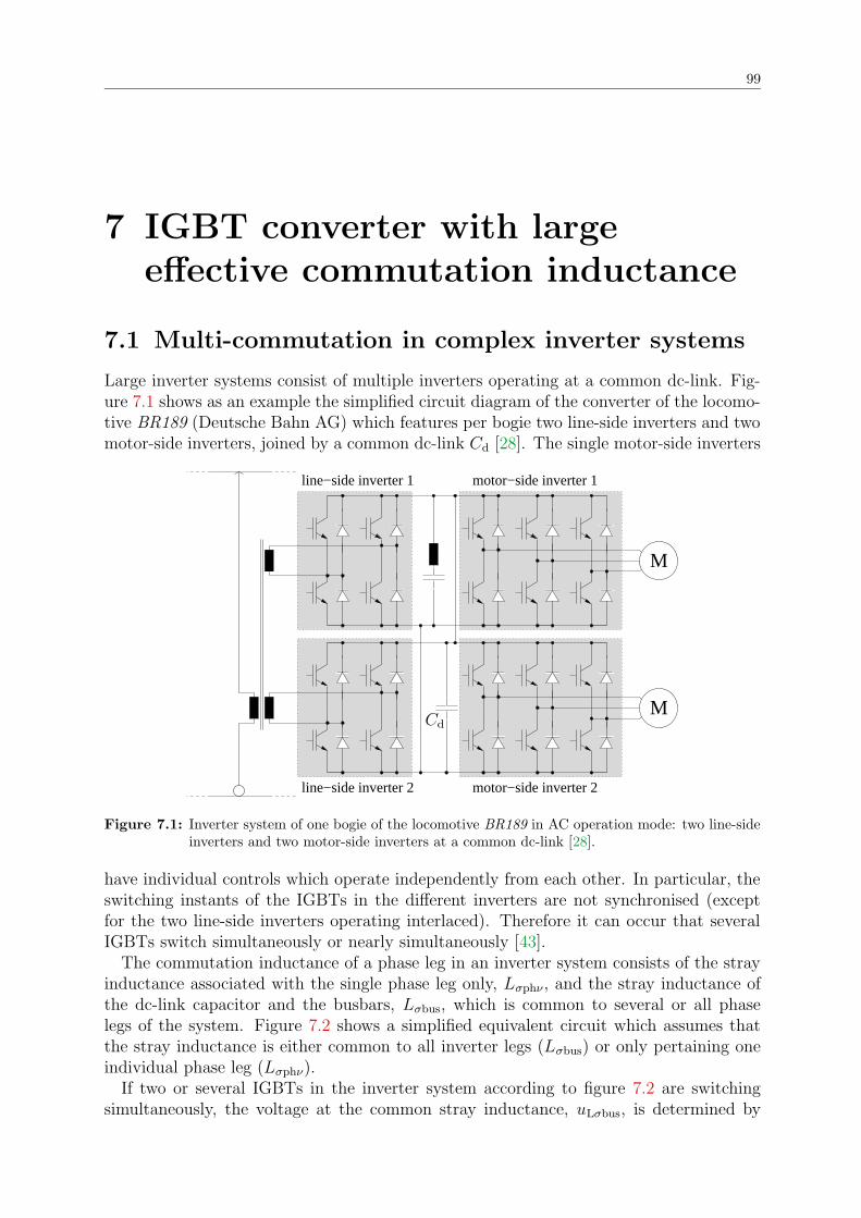
99
7 IGBT converter with largeeffective commutation inductance
7.1 Multi-commutation in complex inverter systems
Large inverter systems consist of multiple inverters operating at a common dc-link. Fig-ure 7.1 shows as an example the simplified circuit diagram of the converter of the locomo-tive BR189 (Deutsche Bahn AG) which features per bogie two line-side inverters and twomotor-side inverters, joined by a common dc-link Cd [28]. The single motor-side inverters
M
M
line−side inverter 1 motor−side inverter 1
line−side inverter 2 motor−side inverter 2
PSfrag replacements
Cd
Figure 7.1: Inverter system of one bogie of the locomotive BR189 in AC operation mode: two line-sideinverters and two motor-side inverters at a common dc-link [28].
have individual controls which operate independently from each other. In particular, theswitching instants of the IGBTs in the different inverters are not synchronised (exceptfor the two line-side inverters operating interlaced). Therefore it can occur that severalIGBTs switch simultaneously or nearly simultaneously [43].
The commutation inductance of a phase leg in an inverter system consists of the strayinductance associated with the single phase leg only, Lσphν , and the stray inductance ofthe dc-link capacitor and the busbars, Lσbus, which is common to several or all phaselegs of the system. Figure 7.2 shows a simplified equivalent circuit which assumes thatthe stray inductance is either common to all inverter legs (Lσbus) or only pertaining oneindividual phase leg (Lσphν).
If two or several IGBTs in the inverter system according to figure 7.2 are switchingsimultaneously, the voltage at the common stray inductance, uLσbus, is determined by

100 CHAPTER 7. CONVERTER WITH LARGE COMMUTATION INDUCTANCE
the sum of the current slopes in the single phase legs. If, for instance, several high-sideswitches turn off simultaneously, the voltage at the common stray inductance uLσbus ishigher compared to the case when only a single switch turns off. Thus the commutationvoltage that has to be provided by the IGBTs is higher in case of multi-commutation sothat simultaneous commutations in multiple phase legs virtually increase the commutationinductance. If n denotes the number of IGBTs switching simultaneously, the voltage atthe total commutation inductance vLσν = uLσbus + uLσph,ν of one phase leg is given by
vLσν = Lσphν ·di
dt+ Lσbus · n · di
dt. (7.1)
The ’effective’ commutation inductance in dependence upon the number of commutatingphase legs n therefore is defined as
L′σν(n) = Lσphν + n · Lσbus. (7.2)
Hence the gate drive of the IGBTs must be designed to assure safe commutation with allpossible effective commutation inductances L′
σν for all load conditions in the whole dc-link voltage range. In doing so the most important quantities to be limited are the peakanode-to-cathode voltage of the IGBT during turn-off, as well as the peak reverse voltageand the peak power dissipation of the diode during turn-on of the IGBT. Section 7.2 dealswith the specifics of the turn-off of ’field-stop’ / ’soft punch-through’ IGBTs with largecommutation inductance. Measures to keep the safe operation area of the diode duringturn-on of the IGBT are discussed in Section 7.3. The new technique of ’active clampingfor the diode’ by means of the antiparallel IGBT is examined in particular.
PSfrag replacements Lσph1 Lσph2 Lσph3 Lσph,nLσbus
Cd
uLσbus
uLσph,n
uph,n
Figure 7.2: Common and individual stray inductances of multiple phase legs operating at a commondc-link.
7.1.1 Experimental approach
The switching behaviour of IGBTs and diodes in case of multi-commutation can be ana-lysed with a simple step-down converter configuration, if the commutation inductance isadjustable. A low value of the commutation inductance represents normal commutation,

7.2. TURN-OFF WITH LARGE COMMUTATION INDUCTANCE 101
while an elevated value simulates multi-commutation. It has to be noted that the exper-iments with this setup do not account for special effects in case of a nearly simultaneousswitching of IGBTs [43].
For the experiment, the nominal commutation inductance was chosen to Lσ = Lσbus +Lσphν = 110 nH assuming Lσbus = 44 nH and Lσphν = 66 nH (Ud = 1.5..2.2 kV, iA,nom =1200 A) . Considering the converter in Figure 7.1, the maximal number of simultaneouscommutations is six: two for each motor-side inverter and one for each line-side inverter.This yields a maximum effective total commutation inductance of L′
σ = 330 nH.
7.2 Turn-off with large commutation inductance
7.2.1 Requirements for a safe turn-off
During turn-off both the maximum rate of rise as well as the maximum value of theanode-to-cathode voltage uAC have to be limited. The former is necessary to prevent adynamic latch-up (Sect. 4.7), the latter to prevent a breakdown of the pn-junction.
The rate of rise of the anode-to-cathode voltage can easily be controlled by the valueof the turn-off gate resistor.
If the commutation inductance is increased, the time integral of the commutation volt-age which has to be provided by the IGBT is increased. At the beginning of the commu-tation, when the anode-to-cathode voltage exceeds the value of the dc-link voltage, uAC
continues to rise until the anode current iA drops significantly. Thus, a larger commu-tation inductance, which delays the falling of iA, leads to higher peak anode-to-cathodevoltages during the commutation. If the commutation inductance is too large, a destruc-tive overvoltage can occur.
As it is known (e.g. [2]), the modern IGBT devices with ’field stop’ / ’soft punch-through’ technology show a drastic reduction of the output capacitance during turn-offwhen the whole low-doped pnp-base is depleted. This leads to a sudden increase of theuAC-slope as can be seen from figures A.4 and A.5 in the Appendix A which show turn-offwaveforms of a ’field-stop’ IGBT in case of an increased commutation inductance. Thereason is that the ’redistribution’ capacitance Ccer (Sect. 4.3) which dominates the turn-off process primarily [39] decays rapidly, when all excess carriers have been swept out ofthe pnp-base. This characteristic largely complicates the handling of overload conditions.As can be seen from Figure A.6, the behaviour of a NPT-type IGBT in the same point ofoperation is much more ’friendly’. The following sections analyse measures to be takenfor a safe switching of field-stop devices in case of an increased effective commutationinductance.
7.2.2 Limiting the overvoltage of ’field-stop’ IGBTs
It is well known that the peak anode-to-cathode voltage of the IGBT can be limited to anadmissible value by acting on the gate, which is referred to as ’active clamping’ [17]. Tothat end, a zener element is connected between anode and gate of the IGBT as depictedin Figure 7.3. The serial diode blocks the current path through the zener diode duringturn-on. If the anode-to-cathode voltage of the IGBT exceeds the threshold voltage ofthe zener element the current of the zener element, iz, largely increases the (negative)current iGD of the gate drive. This raises the voltage drop at the gate resistor RG,off .

102 CHAPTER 7. CONVERTER WITH LARGE COMMUTATION INDUCTANCE
When the voltage drop at RG exceeds the value of uGC − uGD, the IGBT gate is chargedagain and the gate-to-cathode voltage uGC of the IGBT increases. In consequence, thedrain current of the inherent MOSFET is increased. This decreases the component of theelectron current in the pnp-base charging the drain-source space-charge capacitance Cdsj
(Fig. 4.6). The strong feedback stops the increase of the anode-to-cathode voltage of theIGBT.
PSfrag replacements
UGD,off
iG
uRG,off
iz
iCGA
CGA
iGD
Figure 7.3: Active clamping
PSfrag replacements
UGD,off
iG
uRG,off
iz
iCGA
CGA
iGD
Figure 7.4: Active clamping and activesnubbing
Instead of the ’direct’ feedback through the zener element, the current iz could also beused to trigger a switching of the gate-drive voltage to UGD,on. This would reduce thecurrent of the gate driver to the expense of a reduced rise time of the gate-to-cathodevoltage, because of the limited output voltage of the gate drive.
However, for an effective active clamping the gate-to-cathode voltage uGC needs to havea value near the gate-threshold voltage. If uGC has already fallen significantly below thethreshold voltage when the zener element breaks down, the current iz in practice cannotraise uGC above the threshold voltage before the peak anode-to-cathode voltage is reached.This can be seen from Figure 7.5 which shows turn-off waveforms of a 3.3 kV/1200 A’field-stop’ IGBT with planar gate (FZ1200R33KL2, Eupec) at increased commutationinductance. Six suppressor diodes 1.5KE400A (440 V breakdown voltage each) in seriesconnection are used for active clamping. The gate current iG increases rapidly whenthe anode-to-cathode voltage exceeds the threshold voltage of the zener element which isdynamically increased above the static value of 6×400 V = 2400 V due to the charactersiticof the suppressor diodes. At this instance uGC has already fallen to a value below zero.Though the gate-current iG reaches a peak value of 8 A, uGC is not even raised abovezero. Thus, active clamping alone employed with ’field-stop’ devices does not protectagainst destructive overvoltages. This problem is much less severe if NPT-type IGBTsare employed, because their output capacitance is comparatively large at the end of thecommutation period.
It is known that a capacitor between the gate and the anode of the IGBT (fig. 7.4) canbe used to prolong the turn-off plateau of the gate-to-cathode voltage (e.g. [66]). Thegate-anode capacitor CGA adds to the gate-drain capacitance of the inherent MOSFET

7.2. TURN-OFF WITH LARGE COMMUTATION INDUCTANCE 103
und thus increases the negative feedback during turn-off (Subsect. 4.6.3). By this meansuGC can be held on a level near the gate-threshold voltage during the rise of uAC, so thatthe active clamping can become effective.
However, for the ’field-stop’ IGBT used for the experiments it turned out that a success-ful active clamping requires the gate-to-cathode voltage uGC to be even raised above theuGC-plateau level during the rise of the anode-to-cathode voltage uAC. A strong negativefeedback during the rise of uAC is required since the curve of uAC at medium anode-currentlevels shows a saddle point before the peak anode-to-cathode voltage is reached, as can beseen from Figure A.4. If this occurs, the negative feedback through the gate-anode capac-itor vanishes and the gate-to-cathode voltage starts to drop so that the active clampingis defeated. The increase of uGC due to the Cgd feedback during the uAC ramp increasesthe drain current of the inherent MOSFET of the IGBT and thus reduces the rate of riseof the anode-to-cathode voltage uAC. The intentional deceleration of the rise of uAC byacting on the gate of the IGBT is referred to as ’active snubbing’.
Figure 7.6 shows turn-off waveforms of a 3.3 kV/1200 A ’field-stop’ IGBT with planargate (FZ1200R33KL2, Eupec) operated at Ud = 2200 V with Iload = 1200 A. The com-mutation inductance amounts to 330 nH. A 2.5-nF gate-anode feedback capacitor is usedto elevate the gate-to-cathode voltage during the rise of the anode-to-cathode voltage; fordamping a 33-Ω resistor is connected in series with the capacitance. The increase of thegate-to-cathode voltage due to the feedback through CGA reduces the slope of uAC which isbasically not desirable. However, the increased turn-off losses due to the active snubbinghave to be accepted, since otherwise destructive overvoltages would occur in this pointof operation. A zener element consisting of 6 × 1 .5KE400A suppressor diodes is used tolimit the anode-to-cathode voltage; to avoid oscillations a 16-Ω resistor is connected inseries with them.
When the threshold voltage of the zener element is reached, the gate current becomespositive and increases rapidly to a peak value of 10 A. In consequence, the gate-to-cathode voltage is raised to a peak value of ≈ 12 V. It has to be noted that the thresholdvoltage of the suppressor diodes is dynamically increased in case of short pulses (< 1 ms)[106]. Thus the gate current and the gate-to-cathode voltage show a ’rise time’ of 200 nsduring which the increase of the anode-to-cathode voltage continues. In consequence, thestatic ’clamp voltage’ of 2400V will be exceeded significantly so that the anode-to-cathodevoltage reaches 3100 V peak.
The increase of uAC is halted when the additional electron current provided by theinherent MOSFET due to increased uGC eliminates the lack of electron current at thedepletion-layer boundary and thus stops further charging of the depletion-layer capaci-tance (Fig. 4.6, Sect. 4.6.3). Then the negative feedback via the gate-anode capacitorCGA and the gate-drain capacitance Cgd of the inherent MOSFET vanishes and the gatecurrent iG decreases rapidly. As a consequence, the gate-to-cathode voltage uGC quicklydrops approximately to the value before the breakdown of the zener element. During theanode-current ramp, the anode-to-cathode voltage uAC decreases because the clampingvoltage of the suppressor diodes decreases with increasing puls duration.
The decrease of the anode current supports the clamping of uAC because the electroncurrent at the collector edge of the pnp-base is reduced. This is the reason why uGC candecrease slightly during the uAC plateau.
During the anode-current ramp, the gate current of the IGBT takes positive values,though uGC decreases slightly. The currents of the gate-anode capacitor and the gate-

104 CHAPTER 7. CONVERTER WITH LARGE COMMUTATION INDUCTANCE
drain capacitance of the inherent MOSFET are zero because the anode-to-cathode voltageis approximately constant. If only the capacitances are considered, the gate-current shouldbe negative because of the falling uGC. However, due to the anode-current to gate-voltagefeedback (Sect. 4.4) a positive gate current is necessary to avoid the decay of the gate-to-cathode voltage at falling anode current.
7.2.3 Comparison of NPT-type and ’field-stop’ IGBTs
The large increase in turn-off losses due to the active snubbing required for a successfulactive clamping raises the question, whether ’field-stop’ IGBT are still superior to con-ventional NPT IGBTs, if their switching speed has to be reduced significantly to achievesafe operation in large inverter systems with large effective commutation inductance.
Figure 7.7 shows turn-off waveforms of a 3.3 kV/1200 A NPT IGBT (FZ1200R33KF1,Eupec) operated with Ud = 2200 V and Iload = 1200 A. Like in figure 7.6, the commu-tation inductance amounts to 330 nH. For this device no active snubbing is necessary tomaintain uGC above the gate-threshold level during the rise of uAC, because the gate-draincapacitance of the inherent MOSFET is larger. Instead, only a zener element consistingof 6 × 1 .5KE400A suppressor diodes is connected between gate and anode to clamp theanode-to-cathode voltage.
It can be seen that the gate-to-cathode voltage uGC of the NPT-type IGBT dropsvery slowly after the turn-off plateau in the uGC-curve while the gate current remainsapproximately constant. When uAC exceeds the breakdown voltage of the zener element,the gate current becomes positive and the gate-to-cathode voltage is increased. Thisbrings the rise of uAC to halt.
Again, the gate current is positive during the anode-current ramp. For a rough estima-tion it is assumed that the gate current iG is taken completely by the gate-drain capaci-tance Cgd of the inherent MOSFET during the rise of uAC. With duAC/dt = 3000 V/µsand iG = 3.5 A this yields Cgd = 1.16 nF. During the anode-current ramp, the anode-to-cathode voltage uAC decreases with 300 V/µs. The current through Cgd thus amounts toCgd · duAC/dt = 0.35 A. During the same period, the gate-to-cathode voltage decreaseswith 5.5 V/µs. According to the data sheet [49], the input capacitance of this IGBT —which at high anode-to-cathode voltages is predominantly the gate-source capacitanceCgs of the inherent MOSFET — amounts to 150 nF. This yields a current through Cgs
of Cgs · duGC/dt = 0.83 A. The gate current is the difference of the current through Cgd
and the current through Cgs and thus should be negative. As explained before, the rea-son for the positive gate current during the anode-current ramp is the anode-current togate-voltage feedback (Sect. 4.4).
A comparison of the waveforms of the anode-to-cathode voltages in figure 7.6 andFigure 7.7 reveals that the slope of uAC is smaller for the ’field-stop’ IGBT with activeclamping and active snubbing. Nonetheless, in this point of operation which simulatesmulti-commutation in a large converter system by means of an increased commutationinductance of Lσ = 330 nH , the turn-off losses of the ’field stop’ IGBT are only slightlyhigher than those of the NPT-type IGBT, as can be taken from Figure 7.9. The reasonis the long tail current of NPT-type IGBT.
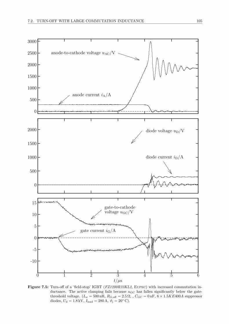
7.2. TURN-OFF WITH LARGE COMMUTATION INDUCTANCE 105
anode current iA/A
anode-to-cathode voltage uAC/V
3000
2500
2000
1500
1000
500
0
diode voltage uD/V
diode current iD/A
2000
1500
1000
500
0
gate current iG/A
voltage uGC/Vgate-to-cathode
t/µs6543210
15
10
5
0
-5
-10
Figure 7.5: Turn-off of a ’field-stop’ IGBT (FZ1200R33KL2, Eupec) with increased commutation in-ductance. The active clamping fails because uGC has fallen significantly below the gate-threshold voltage. (Lσ = 500 nH, RG,off = 2.5Ω, , CGC = 0nF, 6× 1.5KE400A suppressordiodes, Ud = 1.8 kV, Iload = 280A, ϑj = 20 C).

106 CHAPTER 7. CONVERTER WITH LARGE COMMUTATION INDUCTANCE
anode current iA/Avoltage uAC/Vanode-to-cathode
3000
2500
2000
1500
1000
500
0
diode voltage uD/V
diode current iD/A
2000
1500
1000
500
0
gate current iG/A
voltage uGC/Vgate-to-cathode
t/µs1086420
15
10
5
0
-5
-10
Figure 7.6: Turn-off of a ’field-stop’ IGBT (FZ1200R33KL2, Eupec) with active snubbing and activeclamping (Lσ = 330 nH, CGC = 0nF, CGA = 2.5 nF, RG,off = 2.5Ω, Ud = 2.2 kV, Iload =1200A, ϑj = 120 C).

7.2. TURN-OFF WITH LARGE COMMUTATION INDUCTANCE 107
anode current iA/Avoltage uAC/Vanode-to-cathode
3000
2500
2000
1500
1000
500
0
diode voltage uD/V
diode current iD/A
2000
1500
1000
500
0
gate current iG/A
voltage uGC/Vgate-to-cathode
t/µs1086420
15
10
5
0
-5
-10
Figure 7.7: Turn-off of a NPT IGBT (FZ1200R33KF1, Eupec) with active clamping (Lσ = 330 nH,RG,off = 2.5Ω, CGC = 0nF, Ud = 2.2 kV, Iload = 1200A, ϑj = 120 C).
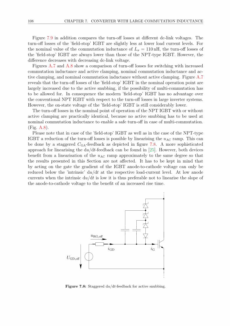
108 CHAPTER 7. CONVERTER WITH LARGE COMMUTATION INDUCTANCE
Figure 7.9 in addition compares the turn-off losses at different dc-link voltages. Theturn-off losses of the ’field-stop’ IGBT are slightly less at lower load current levels. Forthe nominal value of the commutation inductance of Lσ = 110 nH, the turn-off losses ofthe ’field-stop’ IGBT are always lower than those of the NPT-type IGBT. However, thedifference decreases with decreasing dc-link voltage.
Figures A.7 and A.8 show a comparison of turn-off losses for switching with increasedcommutation inductance and active clamping, nominal commutation inductance and ac-tive clamping, and nominal commutation inductance without active clamping. Figure A.7reveals that the turn-off losses of the ’field-stop’ IGBT in the nominal operation point arelargely increased due to the active snubbing, if the possibility of multi-commutation hasto be allowed for. In consequence the modern ’field-stop’ IGBT has no advantage overthe conventional NPT IGBT with respect to the turn-off losses in large inverter systems.However, the on-state voltage of the ’field-stop’ IGBT is still considerably lower.
The turn-off losses in the nominal point of operation of the NPT IGBT with or withoutactive clamping are practically identical, because no active snubbing has to be used atnominal commutation inductance to enable a safe turn-off in case of multi-commutation.(Fig. A.8).
Please note that in case of the ’field-stop’ IGBT as well as in the case of the NPT-typeIGBT a reduction of the turn-off losses is possible by linearising the uAC ramp. This canbe done by a staggered CGA-feedback as depicted in figure 7.8. A more sophisticatedapproach for linearising the du/dt-feedback can be found in [25]. However, both devicesbenefit from a linearisation of the uAC ramp approximately to the same degree so thatthe results presented in this Section are not affected. It has to be kept in mind thatby acting on the gate the gradient of the IGBT anode-to-cathode voltage can only bereduced below the ’intrinsic’ du/dt at the respective load-current level. At low anodecurrents when the intrinsic du/dt is low it is thus preferable not to linearise the slope ofthe anode-to-cathode voltage to the benefit of an increased rise time.
PSfrag replacements
UGD,off
iG
uRG,off
iziCGA
CGA
iGD
Figure 7.8: Staggered du/dt-feedback for active snubbing.

7.2. TURN-OFF WITH LARGE COMMUTATION INDUCTANCE 109
FZ1200R33KF1, Lσ = 150 nH
FZ1200R33KF1, Lσ = 330 nH
FZ1200R33KL2, Lσ = 150 nH
FZ1200R33KL2, Lσ = 330 nH
Turn-off losses at 2200 V dc-link voltage
W/W
s
4
3.5
3
2.5
2
1.5
1
0.5
0
FZ1200R33KF1, Lσ = 150 nH
FZ1200R33KF1, Lσ = 330 nH
FZ1200R33KL2, Lσ = 150 nH
FZ1200R33KL2, Lσ = 330 nH
Turn-off losses at 1800 V dc-link voltage
W/W
s
4
3.5
3
2.5
2
1.5
1
0.5
0
FZ1200R33KF1, Lσ = 150 nH
FZ1200R33KF1, Lσ = 330 nH
FZ1200R33KL2, Lσ = 150 nH
FZ1200R33KL2, Lσ = 330 nH
Turn-off losses at 1500 V dc-link voltage
Iload/A
W/W
s
120010008006004002000
4
3.5
3
2.5
2
1.5
1
0.5
0
Figure 7.9: Comparison of turn-off losses of a ’field-stop’ IGBT a (FZ1200R33KL2) and a NPT IGBT(FZ1200R33KF1 for normal commutation inductance (110 nH) and enlarged commutationinductance (330 nH); ϑj = 120 C.

110 CHAPTER 7. CONVERTER WITH LARGE COMMUTATION INDUCTANCE
7.2.4 Conclusion
The switching speed of fast ’field-stop’ IGBTs has to be decreased significantly to avoiddestructive overvoltages during turn-off with a large commutation inductance. This in-creases the turn-off losses largely, which reduces the attractiveness of these devices (thatare still featuring lower on-state losses).
The manufacturer of the IGBT examined here has already reacted to the problem [11]:Now, two types of IGBTs are offered: a ’fast’ version for inverters with low commutationinductance and a ’soft’ version for converters with large commutation inductance. A’softer’ turn-off behaviour of the IGBTs can be achieved by increase of the wafer thickness,the pnp-base doping concentration, and the emitter efficiency. Wafer thickness and pnp-base doping increase the value of the anode-to-cathode voltage at which the electric fieldreaches the field-stop layer. The improved emitter efficiency increases the excess-carrierconcentration at the anode side of the pnp-base which enlarges the output capacitanceof the IGBT during turn-off at high anode-to-cathode voltages. Furthermore, the higheremitter efficiency raises the fraction of the hole current in the pnp-base. This increasesthe concentration of mobile holes in the depletion layer during turn-off. With the netdoping in the space-charge region thus increased, the uAC level at which the field reachesthe field-stop layer is raised.
The need for increased output capacitance at high uAC levels for a ’soft’ turn-off conflictswith the efforts for levelling the plasma concentration in the pnp-base for the sake of loweron-state losses.
Recently, it was reported that punch-through IGBT can show a ’self-clamp’ character-istic [108]. The underlying mechanism is a dynamic avalanche: The electrons generatedin the space-charge region by avalanche multiplication replace the drain current of theinherent MOSFET and stop the charging of the space-charge capacitance Cdsj (Fig. 4.6).The avalanche generation occurs at the collector-base junction of the pnp-transistor in-herent in the structure of the IGBT (Fig. 4.5) where the electric field strength is highest.The charge of the electrons that are swept towards the anode decreases the net doping ofthe anode which further reduces the anode-to-cathode voltage.
A self-clamping characteristic of IGBT is highly desirable since it removes constraintson the switching speed due to the requirements for active clamping.
The examinations show that the commutation inductance can heavily afflict the switch-ing behaviour of power semiconductor devices. Thus, the significance of characteristicvalues given in technical informations about power semiconductor devices is limited if thecommutation inductance used for the measurements is not quoted.

7.3. TURN-ON WITH LARGE COMMUTATION INDUCTANCE 111
7.3 Turn-on with large commutation inductance
7.3.1 Influence of the commutation inductance on the turn-onwaveforms
Figure 7.10 shows a comparison of turn-on waveforms for different commutation induc-tances with identical gate-drive (UGD,on = 15 V, UGD,off = −9 V, RG,on = 1.0 Ω) andload (Ud = 2200 V, Iload = 1200 A) conditions. The commutation inductances amount toLσ = 110 nH and Lσ = 330 nH, respectively. Top down the Figure compares the anode-to-cathode voltages of the switching IGBT, the diode currents, the diode voltages andthe waveforms of the power dissipation of the diodes. It can be seen that the slope ofthe diode current iD is smaller with a larger commutation inductance Lσ. However, therate of fall of iD is not proportional to the reciprocal value of Lσ since the commutationvoltage, which is the difference of the dc-link voltage Ud and the anode-to-cathode of theIGBT uAC, increases with increasing commutation inductance. The reason is that uAC
drops faster with a large commutation inductance since the anode-current level duringthe current ramp is lower compared to the case with the smaller commutation inductance.That way a greater portion of the drain current of the MOSFET inherent in the structureof the IGBT can discharge the depletion layer capacitance (Sect. 4.6).
Due to the slightly lower diode-current gradient in case of a larger commutation induc-tance, the removal of the stored charge is completed at a slightly lower reverse currentlevel at t2 while in case of the lower commutation inductance uD starts to rise at a slightlylarger reverse current at t1 (Fig. 7.10). Consequently the initial rate of rise of the diodevoltage uD during the first 100 ns is lower in case of low commutation inductance, sincethe current that is charging the output capacitance of the diode is smaller. The end ofthe storage phase of the diode is marked by a vertical line for both cases in Figure 7.10.
The rising diode voltage reduces the voltage at the commutation inductance Lσ. Incase of the small commutation inductance the voltage at Lσ becomes zero earlier afterthe beginning of the diode current rise since the initial slope of uD is steeper and becausethe anode-to-cathode voltage of the IGBT is higher, as discussed before. With a largercommutation inductance the instant of the peak reverse current is delayed, since theanode-to-cathode voltage of the IGBT is lower and because of the smaller initial gradientof the diode voltage uD. For that reason the peak reverse current of the diode is evenlarger with the increased commutation inductance despite the lower current gradient! Thehigher reverse current leads to a steeper increase of the diode voltage which accounts forthe fact that the rate of rise of the diode current iD after the reverse current peak issteeper with the large commutation inductance.
During the commutation of the reverse current the behaviour specific for punch-throughdiodes can be observed in case of the large commutation inductance. When the reversecurrent reduces due to the voltage at the commutation inductance, the concentration ofmobile holes in the depletion layer of the diode decreases which lessens the rate of riseof the diode voltage uD. The gradient of uD becomes zero when this effect compensatesthe charging of the output capacitances of the diode by the remaining reverse current.All excess carriers have been removed when the boundary of the depletion layer ’punchesthrough’ to the cathode of the diode. This eliminates the contribution of mobile holesto the diode voltage, but largely decreases the output capacitance. In consequence thegradient of the diode voltage increases rapidly which increases the absolute value of the

112 CHAPTER 7. CONVERTER WITH LARGE COMMUTATION INDUCTANCE
Lσ = 330 nH
Lσ = 110 nH
IGBT anode-to-cathode voltages / V
2000
1500
1000
500
0
Lσ = 330 nH
Lσ = 110 nH
Diode currents / A
1000
500
0
-500
-1000
t2t1
Lσ = 330 nH
Lσ = 110 nH
Diode voltages / V
2000
1500
1000
500
0
Lσ = 300 nH
Lσ = 100 nH
Diode power dissipations / kW
6543210
1000
500
0
Figure 7.10: Comparison of IGBT turn-on waveforms with different commutation inductances(FZ1200R33KL2, Eupec, RG,on = 1.0Ω, CGC = 680 nF, Ud = 2.2 kV, Iload = 1200A,ϑj = 120 C))
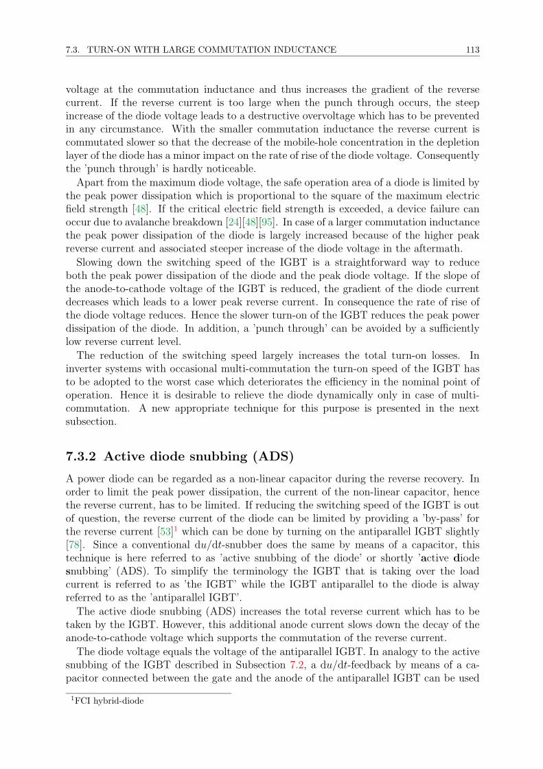
7.3. TURN-ON WITH LARGE COMMUTATION INDUCTANCE 113
voltage at the commutation inductance and thus increases the gradient of the reversecurrent. If the reverse current is too large when the punch through occurs, the steepincrease of the diode voltage leads to a destructive overvoltage which has to be preventedin any circumstance. With the smaller commutation inductance the reverse current iscommutated slower so that the decrease of the mobile-hole concentration in the depletionlayer of the diode has a minor impact on the rate of rise of the diode voltage. Consequentlythe ’punch through’ is hardly noticeable.
Apart from the maximum diode voltage, the safe operation area of a diode is limited bythe peak power dissipation which is proportional to the square of the maximum electricfield strength [48]. If the critical electric field strength is exceeded, a device failure canoccur due to avalanche breakdown [24][48][95]. In case of a larger commutation inductancethe peak power dissipation of the diode is largely increased because of the higher peakreverse current and associated steeper increase of the diode voltage in the aftermath.
Slowing down the switching speed of the IGBT is a straightforward way to reduceboth the peak power dissipation of the diode and the peak diode voltage. If the slope ofthe anode-to-cathode voltage of the IGBT is reduced, the gradient of the diode currentdecreases which leads to a lower peak reverse current. In consequence the rate of rise ofthe diode voltage reduces. Hence the slower turn-on of the IGBT reduces the peak powerdissipation of the diode. In addition, a ’punch through’ can be avoided by a sufficientlylow reverse current level.
The reduction of the switching speed largely increases the total turn-on losses. Ininverter systems with occasional multi-commutation the turn-on speed of the IGBT hasto be adopted to the worst case which deteriorates the efficiency in the nominal point ofoperation. Hence it is desirable to relieve the diode dynamically only in case of multi-commutation. A new appropriate technique for this purpose is presented in the nextsubsection.
7.3.2 Active diode snubbing (ADS)
A power diode can be regarded as a non-linear capacitor during the reverse recovery. Inorder to limit the peak power dissipation, the current of the non-linear capacitor, hencethe reverse current, has to be limited. If reducing the switching speed of the IGBT is outof question, the reverse current of the diode can be limited by providing a ’by-pass’ forthe reverse current [53]1 which can be done by turning on the antiparallel IGBT slightly[78]. Since a conventional du/dt-snubber does the same by means of a capacitor, thistechnique is here referred to as ’active snubbing of the diode’ or shortly ’active diodesnubbing’ (ADS). To simplify the terminology the IGBT that is taking over the loadcurrent is referred to as ’the IGBT’ while the IGBT antiparallel to the diode is alwayreferred to as the ’antiparallel IGBT’.
The active diode snubbing (ADS) increases the total reverse current which has to betaken by the IGBT. However, this additional anode current slows down the decay of theanode-to-cathode voltage which supports the commutation of the reverse current.
The diode voltage equals the voltage of the antiparallel IGBT. In analogy to the activesnubbing of the IGBT described in Subsection 7.2, a du/dt-feedback by means of a ca-pacitor connected between the gate and the anode of the antiparallel IGBT can be used
1FCI hybrid-diode
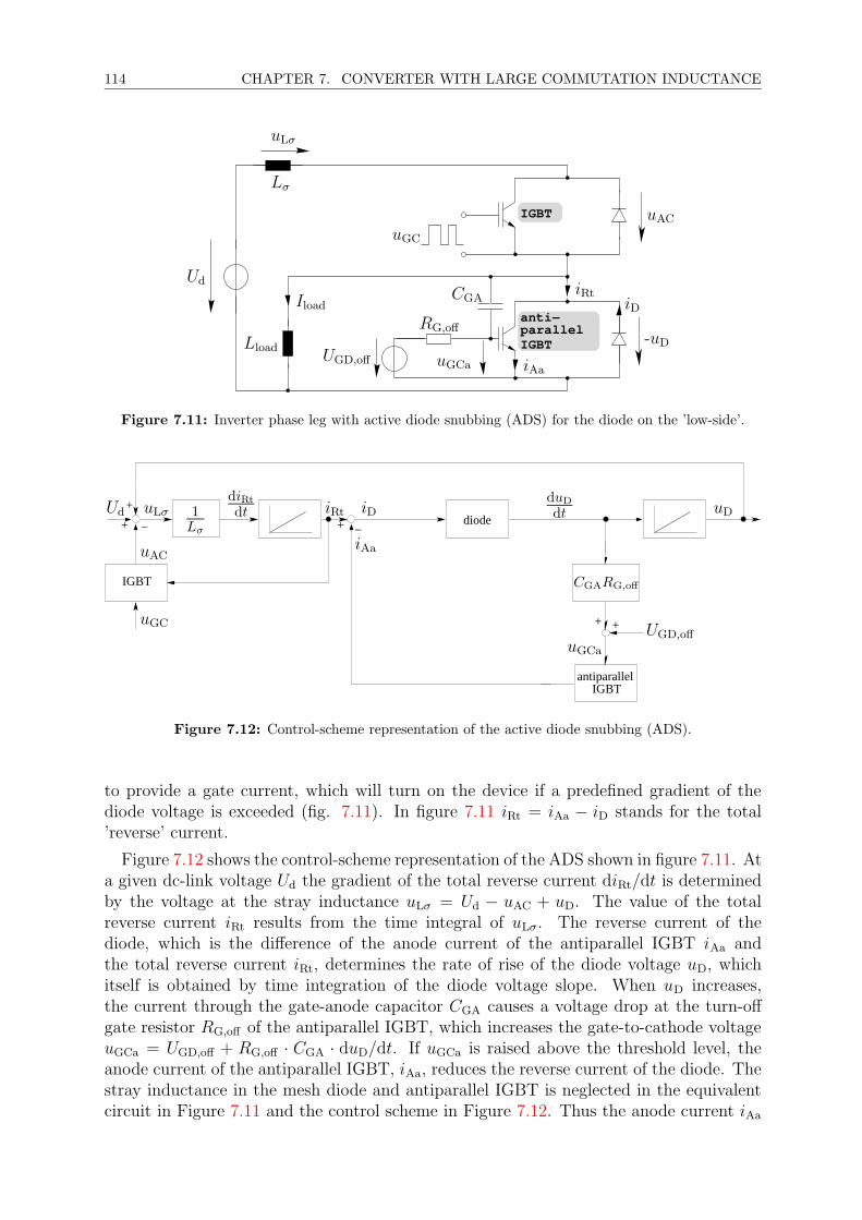
114 CHAPTER 7. CONVERTER WITH LARGE COMMUTATION INDUCTANCE
anti−parallelIGBT
IGBT
PSfrag replacements
anodecathode
gatescope
CGA
uGCa
iA,PPI
uAC
uAC,PPI
uGC,PPI
uGC
UGD,off
Ud
-uD
Iload
iD
iAa
iRt
iG,PPI
iG,PPI
RG,off
RGi
UGDoff,PPI
−15 VLσ
uLσ
duLσ
dt
Lσ,module
Lσ,PPI
CGA,PPI
iCGA,PPI Lload
Iload
Figure 7.11: Inverter phase leg with active diode snubbing (ADS) for the diode on the ’low-side’.
diode
IGBTantiparallel
+ +
− −
+
++
IGBT
PSfrag replacements
anodecathode
gatescopeCGA
uGCa
iA,PPI
uAC
uAC,PPI
uGC,PPI
uGC
UGD,off
Ud
-uD
Iload
iDiAa
iRt
iG,PPI
iG,PPI
RG,off
RGi
UGDoff,PPI
−15 VLσ
uLσduLσ
dt
Lσ,module
Lσ,PPI
CGA,PPI
iCGA,PPI
Lload
Iload
CGARG,off
iAauAC
UGD,off
Ud uLσ 1Lσ
uDiDiRt
diRt
dt
uGCa
duD
dt
Figure 7.12: Control-scheme representation of the active diode snubbing (ADS).
to provide a gate current, which will turn on the device if a predefined gradient of thediode voltage is exceeded (fig. 7.11). In figure 7.11 iRt = iAa − iD stands for the total’reverse’ current.
Figure 7.12 shows the control-scheme representation of the ADS shown in figure 7.11. Ata given dc-link voltage Ud the gradient of the total reverse current diRt/dt is determinedby the voltage at the stray inductance uLσ = Ud − uAC + uD. The value of the totalreverse current iRt results from the time integral of uLσ. The reverse current of thediode, which is the difference of the anode current of the antiparallel IGBT iAa andthe total reverse current iRt, determines the rate of rise of the diode voltage uD, whichitself is obtained by time integration of the diode voltage slope. When uD increases,the current through the gate-anode capacitor CGA causes a voltage drop at the turn-offgate resistor RG,off of the antiparallel IGBT, which increases the gate-to-cathode voltageuGCa = UGD,off + RG,off · CGA · duD/dt. If uGCa is raised above the threshold level, theanode current of the antiparallel IGBT, iAa, reduces the reverse current of the diode. Thestray inductance in the mesh diode and antiparallel IGBT is neglected in the equivalentcircuit in Figure 7.11 and the control scheme in Figure 7.12. Thus the anode current iAa

7.3. TURN-ON WITH LARGE COMMUTATION INDUCTANCE 115
is directly related to the gate-to-cathode voltage.The CGARG,off-feedback establishes basically a proportional controller with the set point
determined by the product of CGA and RG,off . The gap between the threshold voltage ofthe antiparallel IGBT and the gate drive voltage UGD,off causes a wide dead band of thecontrol system. With uGCa above the threshold level the controller amplification is onlydetermined by the transfer characteristic of the antiparallel IGBT.
Unfortunately, the gradient of the diode voltage during the reverse recovery decreaseswith increasing load current level. Thus the du/dt-feedback provided by the gate-anodecapacitor of the antiparallel IGBT is the weaker the more it is needed. This is especiallyrelevant for switching with zero load current when the slope of the diode voltage is verysteep since its output capacitance is small due to the lack of excess carriers. However,the slope of the diode voltage increases if the commutation inductance is increased due tomulti-commutation as seen in Figure 7.10. Hence it is possible to parameterise the ADSin such a way, that the active snubbing is not triggered in the nominal point of operation(low commutation inductance) for a wide load-current range, but becomes active only ifthe commutation inductance increases due to multi-commutation. Still, in the nominaloperation point the active snubbing of the diode inevitably increase the turn-on losses ifthe anode current is low (or zero).
ADS does not conflict with the active clamping for turn-off because the respectivesetpoint values for the du/dt-feedback control can be chosen independently by means ofdifferent gate resistors for turn-on and turn-off.
7.3.3 Experimental setup for ADS
Most IGBT devices are packed in plastic-mould modules which also contain the antipar-allel diode. At the terminals only the sum of diode current and IGBT current can bemeasured. However, the diode current must be known for dimensioning the ADS to limitthe peak power dissipation. One option is to provide tiny Rogowski coils for each diodechip inside the device. While this is feasible in principle, it is a very challenging task inhigh-voltage devices due to insulation requirements.
Alternatively, it was proposed that for an experimental setup the IGBT in the powermodule is blocked permanently, while an additional IGBT device which does not containan antiparallel diode is used for the active snubbing of the diode [57]. Fortunately, press-pack IGBT devices are available without internal diode. This approach was adopted forthis work. A setup that connects a press-pack IGBT (PPI) in parallel to an IGBT moduleis shown in Figure 7.13. The diode current and the current of the antiparallel PPI aremeasured with small high-frequency coaxial shunts (Section B.4.2). An equivalent circuitof the setup is depicted in figure 7.14. In this setup, the inductance of the mesh builtby the diode and the antiparallel PPI (Lσ,diode + Lσ,PPI) is an order of magnitude largerthan that in the plastic module. Thus the inductance of the mesh retards the relief of thediode by means of the antiparallel IGBT. Therefore the experimental setup represents theworst case for an ADS.
The value of the inductance of the mesh built by the PPI and the diode in the plasticmodule was calculated to Lm = Lσ,mod +Lσ,PPI = 40 nH from measurements of the anode-to-cathode voltages of the devices and the anode current of the PPI. The introduction ofLm changes the control system shown in Figure 7.12 to a certain degree. The resultingcontrol scheme is depicted in figure 7.15. Because of Lm an increase of the gate-to-cathode

116 CHAPTER 7. CONVERTER WITH LARGE COMMUTATION INDUCTANCE
anode cathode
anode cathode
shunts
PPI
plastic module
PSfrag replacements
−Ud
+Ud
(a) side view
module cathodePPI cathodePPI anode
!!"" ##$$%%&&
PPI current
diode current
''''''''''''''''''''''''''''''
((((((((((((((((((((((((((((((
))))))))))))
************
++++++++++++++++++++++++++++++
,,,,,,,,,,,,,,,,,,,,,,,,,,,,,,
PPI
PSfrag replacements
−Ud
+Ud
(b) top view
Figure 7.13: Measurement setup with press-pack IGBT parallel to plastic-module IGBT device withinternal antiparallel diode. The IGBT in the module is permanently blocked.
voltage of the antiparallel PPI does not result in an increase of the anode current iA,PPI
directly. In fact the gate-to-cathode voltage influences the slope of the anode-to-cathodevoltage uAC,PPI which is moreover affected by the anode current iA,PPI. The anode currentof the PPI is the time integral of the difference of the diode voltage uD and uAC,PPI.
It has to be noted that the output capacitance of the PPI adds to the output capacitanceof the diode and the IGBT in the plastic module which slightly changes the switchingwaveforms even if the PPI is permanently blocked.
The IGBT power module under test is a FZ1200R33KL2 (Eupec) rated 3300 V/1200 A.The maximum allowable power dissipation of the internal diode is PRQM = 1200 kW. AToshiba S2996 press-pack IGBT rated 4500 V/2000 A [56] is used for ADS. Unlike thedevice presented in [56] the press-pack IGBT used here does not contain diode chips.
The gate-drive parameters of the IGBT are listed in Table 7.1. These are chosen for safecommutation at the nominal commutation inductance without active snubbing applied.As indicated before, ADS will affect the switching in the nominal point of operation, too.However, the parameters in Table 7.1 do not anticipate the effect of the active snubbingon the switching with nominal commutation inductance.
7.3.4 Measurements
7.3.4.1 Active snubbing of the diode with negative static gate bias for theantiparallel IGBT
Figure 7.16 shows turn-on waveforms with ADS at Ud = 2200 V and Iload = 1200 A . Thecommutation inductance amounts to 330 nH which represents multi-commutation. The

7.3. TURN-ON WITH LARGE COMMUTATION INDUCTANCE 117
module #1
PPImodule #2
PSfrag replacements
anodecathode
gatescope
iA,PPIiRt
uAC
uAC,PPI
uGC,PPI
uGC
UduD
Iload
iD
iG,PPI
iG,PPI RGoff,PPIRGi
UGDoff,PPI
−15 V
Lσ0
Lσ,mod Lσ,PPI
CGA,PPI
iCGA,PPI
Lload
Iload
RshuntRshunt
Figure 7.14: Equivalent circuit representation of the measurement setup for the examination of ADS.
diode
IGBTantiparallel
RC
+ +
− +
− −
+
++
IGBT
PSfrag replacements
anodecathode
gatescopeiA,PPI
iRt
uAC
uAC,PPI
uGC,PPI
uGC
Ud
uD
Iload
iDiG,PPI
iG,PPI
RGoff,PPI
RGi
UGDoff,PPI
−15 VLσ0
Lσ,mod
Lσ,PPI
CGA,PPI
iCGA,PPI
Lload
Iload
Rshunt
anodecathode
gatescopeCGA
uGCa
iA,PPI
uAC
uAC,PPI
duAC,PPI
dt
uGC,PPI
uGC
UGD,off
Ud
uD
Iload
iDiAa
iRt
iG,PPI
iG,PPI
RG,off
RGi
UGDoff,PPI
−15 VLσ
uLσduLσ
dt
Lσ,mod
1Lm
1Lσ
CGA,PPI
iA,PPI
uAC
uGC UGD,off
Ud uLσ 1Lσ
uDiDiRt
diRt
dt
uGC,PPI
duD
dt
Figure 7.15: Control-scheme representation of ADS accounting for the stray inductance in the mesh(diode / antiparallel IGBT).

118 CHAPTER 7. CONVERTER WITH LARGE COMMUTATION INDUCTANCE
Table 7.1: Gate-drive parameters of the IGBT in the module # 1 (Fig. 7.14) used for the examinationof the ADS
RG,on 1.0 ΩRG,off 2.5 ΩUGD,on 15 VUGD,off −9 VCGA 3.3 nFCGC 330 nF
press-pack IGBT antiparallel to the diode is blocked statically with a negative gate bias ofUGDoff,PPI = −11 V. The turn-off gate resistor of the PPI is RGoff,PPI = 2.5 Ω. The internalgate resistance of the press-pack device is only 54 mΩ 2 and thus negligible. A gate-to-anode feedback capacitor CGA,PPI = 4.05 nF is used to turn on the PPI if the gradientof the diode voltage, which equals the anode-to-cathode voltage of the PPI, exceeds aspecified value.
The first graph in Figure 7.16 shows the anode-to-cathode voltages of the devices. Whenthe anode-to-cathode voltage of the IGBT, uAC, starts to decrease at t0, a commutationvoltage occurs at the total commutation inductance Lσ = Lσ0 +Lσ,diode (c.p. figure 7.14).In consequence, the diode current starts to fall as can be seen from the second graph fromtop in Figure 7.16.
The part of the commutation voltages which drops at Lσ,mod increases the anode-to-cathode voltage of the antiparallel PPI by some 25 V as can be seen from the top graph.This causes a small displacement current through its output capacitance which is visiblein the waveform of the PPI anode current iA,PPI. A part of this current flows through thegate-drain capacitance Cgd of the inherent MOSFET (Fig. 4.6). Cgd is large due to thelow anode-to-cathode voltage and thus outranges the gate-anode capacitance CGA duringthis period. The current through Cgd is for the most part drained through the gate ascan be seen from the negative gate current in the third graph in figure 7.16. The voltagedrop at the gate resistance RGoff,PPI due to the negative gate current increases the gate-to-cathode voltage uGC,PPI = UGDoff,PPI − RGoff,PPI · iG,PPI so that the remaining portionof the current through Cgd that is not drained by the gate drive charges the gate-sourcecapacitance Cgs of the inherent MOSFET (fig. 4.6). This is the reason why the gate-to-cathode voltage of the PPI is raised substantially at the beginning of the diode-currentramp. Throughout the current ramp (t0...t2) uGC,PPI decreases since the voltage at thestray inductance Lσ,mod increases only slightly, so that the displacement current of Cgd
is drastically reduced, while the gate-source capacitance Cgs of the inherent MOSFET isdischarged through the gate.
When the diode voltage uD starts to rise at t1, the gate-to-cathode voltage of the PPIincreases again due to the du/dt-feedback which is caused by the voltage drop at RGoff,PPI
due to the current through Cgd and CGA. With increasing diode voltage, the value of Cgd
reduces drastically so that CGA becomes dominant. Because of the voltage at the strayinductance Lσ,mod the anode-to-cathode voltage of the PPI exceeds the diode voltage aslong as the PPI is blocking. When uGC,PPI reaches the threshold level at t2, the gate-
2The internal gate resistance of the press-pack IGBTs used for the examination of ADS differs fromthat of the PPIs examined in the Sections 4.4, 4.5 and 6.4, though the devices bear the same typedesignation

7.3. TURN-ON WITH LARGE COMMUTATION INDUCTANCE 119
t4t3t2t1t0
uAC,PPI (anode-to-cathode voltage PPI) / V
uAC (anode-to-cathode voltage IGBT) / V
-uD (diode voltage) / V
2500
2000
1500
1000
500
0
iRt = iD − iA,PPI / A
iA,PPI (anode current PPI) / A
iD (diode current) / A
1000
500
0
−500
−1000
iG,PPI (gate current PPI) / A
uGC,PPI (gate-to-cathode voltage PPI) / V15
10
5
0
−5
−10
−15
PRQ (power dissipation diode) / kW
t/µs87654321
1000
500
0
Figure 7.16: ADS at high load current with large commutation inductance / multi-commutation. (Lσ = 330 nH, Ud = 2200V, Iload = 1200A, UGDoff,PPI = −11V, CGA,PPI = 4.05 nF,RGoff,PPI = 2.5Ω, ϑj = 120 C)

120 CHAPTER 7. CONVERTER WITH LARGE COMMUTATION INDUCTANCE
drain capacitance of the inherent MOSFET of the PPI is discharged by the drain current(Fig. 4.6) so that the gradient of uAC,PPI decreases. When the diode voltage exceedsthe anode-to-cathode voltage of the PPI, a ’commutation voltage’ appears at Lσ,mod andLσ,PPI which causes an increase of the anode current of the PPI, iA,PPI, and a decrease ofthe diode current iD. It can be seen from Figure 7.16 that iA,PPI increases for uAC,PPI < uD
in the interval (t2...t3) and decreases for uAC,PPI > uD in the interval (t3...t4), while thegradient of iA,PPI is zero at the intersections of the waveforms of uD and uAC,PPI. It hasto be mentioned that actually the anode-to-cathode voltage of the PPI is used for thedu/dt-feedback which is reflected in the correlation of uAC,PPI and uGC,PPI.
The press-pack IGBT antiparallel to the diode takes over current at t2 and thus reducesthe reverse current of the diode just in time to prevent the power dissipation of the diodeto exceed the admissible value of 1200 kW, as can be seen from the bottom graph inFigure 7.16. The reduction of the diode current due to the active snubbing also reducesthe rate of rise of the diode voltage which helps to limit the power dissipation, too.
During the rise of the anode current of the PPI both the diode voltage and the anode-to-cathode voltage of the PPI do not increase anymore. Concerning the diode this iscaused by the reduction of the reverse current which decreases the density of mobileholes in the depletion layer. The gradient of the anode-to-cathode voltage of the PPI isprimarily determined by the relation of the drain current of the inherent MOSFET andthe electron base current (fig. 4.6)3. The decrease of uAC,PPI due to the drain current ofthe inherent MOSFET is counteracted by the increase of the anode current iA,PPI so thatuAC,PPI ceases to increase, when id and the electron portion of the base current canceleach other (Fig. 4.6).
It is important to note that the gradient of the anode current of the PPI is determinedby the voltage of the stray inductance in the mesh diode/PPI. Hence the gate-to-cathodevoltage of the PPI, uGC,PPI, determines the anode current iA,PPI only indirectly. After thepeak in the PPI anode current at t3, uAC,PPI and −uD increase nearly linearly, but withslightly different slopes while uAC,PPI exceeds −uD which causes the negative gradient ofiA,PPI.
If the total reverse current iRt = iD− iA,PPI would be constant during the rise of uD, thediode and the PPI would share the total current according to their output capacitances,with the output capacitance of the PPI being determined by the level of the gate-to-cathode voltage, which is proportional to the gradient of uAC,PPI due to the feedbackthrough the gate-to-anode capacitor CGA,PPI. Hence the feedback capacitor represents aproportional controller.
The decrease of the total reverse current iRt = iD − iA,PPI is a disturbance for thedu/dt-control. It slows down the rate-of rise of uAC,PPI/ −uD and causes a decrease of thegate-to-cathode voltage of the PPI. With uGC,PPI reduced, the slope of uAC,PPI increasesso that uAC,PPI exceeds uD. This causes a voltage at the stray inductance in the meshwhich commutates the anode current of the PPI gradually back to the diode. That way,the gradient of the diode voltage is kept approximately constant, despite the decreasingtotal reverse current.
As mentioned above, the active snubbing increases the current of the IGBT in themodule #1 (Fig. 7.14), which reduces the gradient of its anode-to-cathode voltage uAC.The increase of uAC of this module helps to ’commutate’ the total reverse current.
3The current of Cgd is neglected here

7.3. TURN-ON WITH LARGE COMMUTATION INDUCTANCE 121
The premature increase of uAC,PPI during the diode-current ramp due to the strongCgd feedback at low anode-to-cathode voltages is very beneficial in the operation point ofFigure 7.16, since the delay time t1−t0 from the beginning of the diode current ramp to theinstant when the gate-to-cathode voltage of the PPI exceeds the threshold level is reduced.Without the premature increase of uGC,PPI, a stronger actuating signal would be neededto limit the reverse current of the diode in time before the maximum power dissipationis exceeded. Since the gain of the ’actuator’ which is the PPI cannot be increased, theonly way to increase the actuating signal is to increase the system deviation by means ofa lower setpoint value. This would needlessly slow down the rest of the switching processand hence cause unnecessary additional losses.
The time period between the beginning of the diode current ramp which is associatedwith the premature increase of uGC,PPI and the beginning of the rise of the diode blockingvoltage uD depends on the load current level. If the load current has a lower value, theduration of the current ramp is shorter and uD rises earlier due to the lower amount ofstored charge. In Figure 7.16 the value of the gate-to-cathode voltage of the PPI, uGC,PPI,shows a local maximum in the interval (t0...t1) before the diode voltage starts to rise. If theload current is reduced so that uD starts to rise earlier after the beginning of the currentramp, the ’initial’ gate-to-cathode voltage of the PPI increases, which decreases the ’deadband’ of the control system established by the du/dt-feedback. Hence the du/dt-feedbackis activated earlier.
In addition, the initial slope of the diode voltage is increased with decreasing load-current level. Consequently, the active snubbing in this setup is more effective at lowload current levels as can be seen from Figure 7.17 which shows turn-on waveforms withADS at Ud = 2200 V and Iload = 100 A. Hence, this technique for active snubbing ofthe diode causes unnecessary losses at low load-current levels since the gradient of thediode voltage is reduced, although the maximum power dissipation of the diode is farbelow its limit. However, it has to be kept in mind that this also applies if the peak powerdissipation of the diode and the maximum diode voltage are controlled by means of slowerswitching speed of the IGBT. The ’transversal’ current through the IGBT antiparallel tothe diode becomes large during turn-on with zero load current, too. In this case theoutput capacitance of the diode is very small due to the lack of excess carriers. Thus thereverse current which builds up the diode voltage is almost zero. To control the slope ofthe diode voltage, the PPI has to take over a huge current to drain the reverse currentfrom the diode. This can be seen from Figure A.9.
In the nominal point of operation, i.e. if the commutation inductance is low, the reversecurrent decays faster. Hence the rate of rise of the diode voltage uD is lower than in caseof multi-commutation, so that the transversal current through the antiparallel IGBT isreduced. With nominal commutation inductance, the ’intrinsic’ gradient of uD at highload-current levels is lower than the maximum gradient determined by the active snubbing.In consequence, the current of the antiparallel IGBT is zero for most of the diode-voltageramp as can be seen from Figure A.10. However, it can be seen from Figure A.11 thatat low load-current levels the active snubbing becomes much more effective since theslope of the diode voltage increases due to the reduced output capacitance of the diode.Consequently active snubbing, which is required for safe commutation in case of multi-commutation reduces the switching speed and thus increases the switching losses in thenominal point of operation.

122 CHAPTER 7. CONVERTER WITH LARGE COMMUTATION INDUCTANCE
(anode-to-cath. volt. PPI) / VuAC,PPI
uAC (anode-to-cathode voltage IGBT) / V
-uD (diode voltage) / V
2500
2000
1500
1000
500
0
iRt = iD − iA,PPI / A
iA,PPI (anode current PPI) / A
iD (diode current) / A
1000
500
0
−500
−1000
iG,PPI (gate current PPI) / A
uGC,PPI (gate-to-cathode voltage PPI) / V15
10
5
0
−5
−10
−15
PRQ (power dissipation diode) / kW
t/µs87654321
1000
750
500
250
0
Figure 7.17: ADS at low load current with large commutation inductance / multi-commutation. (Lσ =330 nH, Ud = 2200V, Iload = 100A, UGDoff,PPI = −11V, CGA,PPI = 4.05 nF, RGoff,PPI =2.5Ω, ϑj = 120 C)

7.3. TURN-ON WITH LARGE COMMUTATION INDUCTANCE 123
7.3.4.2 Active snubbing of the diode with zero static gate bias for theantiparallel IGBT
It could be seen from Figure 7.16 that the difference between the static gate voltageand the gate-threshold voltage of the antiparallel IGBT introduces a dead-band intothe control system for the active snubbing of the diode, which increases the rise time.Unfortunately it is not feasible to increase the control amplification in this completelypassive feedback system to reduce the impact of the dead-band. The product of the valueof the feedback capacitance and the turn-off gate resistor (CGA,PPI ·RGoff,PPI) determinesthe setpoint value, while the control amplification is only determined by the transfercharacteristic of the PPI. In Figure 7.16 the lack of control amplification is compensatedfor by an increase of the system deviation which is achieved by decreasing the du/dt-setpoint value. In consequence the gradient of the diode voltage is determined rather bythe rise time of the gate-to-cathode voltage of the antiparallel IGBT than by the maximumpower dissipation of the diode during the rest of the diode-voltage ramp. Hence the slopeof the diode voltage is decreased more than necessary.
The dead-band and thus the rise time of the control system can be reduced by in-creasing the static gate-to-cathode voltage level of the antiparallel IGBT. However, inthe measurement setup described in Subsection 7.3.3 the turn-off gate drive voltage mustnot be too close to the gate-threshold voltage since otherwise the antiparallel IGBT isturned on already during the diode-current ramp. To prevent a premature turn-on of theantiparallel IGBT due to the voltage drop at Lσ,mod (cp. Fig. 7.14), the turn-off gateresistor can be decreased which allows to choose the turn-off gate-drive voltage somewhathigher. Doing so the feedback capacitor CGA,PPI has to be chosen accordingly larger tokeep the du/dt-setpoint value. Please note that the problem of premature turn-on of theantiparallel IGBT is much less severe if the IGBT in the same power module containingthe diode is used for the active snubbing of the diode, because the stray inductance inseries to the diode is significantly smaller.
Figure 7.18 shows waveforms of a turn-on at Ud = 2200 V and Iload = 1200 A withADS with zero gate bias for the antiparallel IGBT. The turn-off gate resistor is chosenRGoff = 0.5 Ω, while the feedback capacitor is CGA,PPI = 6.75 nF. The commutationinductance amounts to 330 nH which represents multi-commutation. It can be seen thatthe gate resistor is just small enough to drain the displacement current of the gate-draincapacitance of the inherent MOSFET of the PPI during the diode current ramp withoutraising the gate-to-cathode voltage above the threshold level. To prevent a prematureturn-on of the PPI it is very important that the impedance of the gate circuit wiring isextremely low. Otherwise the displacement current of the gate-drain capacitance of thePPI cannot be drained during the diode-current ramp. For the same reason, it is notfeasible to measure the gate current because of the inductance introduced into the gatecircuit by the current probe. Furthermore, a too large inductance in the gate circuit canlead to serious oscillations if the value of the gate resistor is too small. Therefore thecurrent of the gate-anode capacitor CGA,PPI is measured instead of the gate current inFigure 7.18.
In comparison with Figure 7.16 it can be seen that after the beginning of the diode-voltage ramp the gate-to-cathode voltage of the PPI reaches the threshold level earlierdue to the smaller gap between threshold voltage and static gate bias. In consequence,the peak reverse current of the diode is reduced since ADS sets in earlier. The slope of the

124 CHAPTER 7. CONVERTER WITH LARGE COMMUTATION INDUCTANCE
diode voltage is steeper than in Figure 7.16 because of the higher setpoint value. This alsodecreases the peak of the total reverse current iRt since the voltage at the commutationinductance increases faster. The anode current of the PPI decays again when the reversecurrent of the diode has been reduced enough to keep the gradient of the diode voltagebelow the limit imposed by the active snubbing. The steeper increase of the diode voltageleads to a higher turn-off energy of the diode (area under the PRQ-curve), which meansthat the diode is utilised better while the peak power is the same.
As a matter of course the reduced du/dt-setpoint value also decreases the PPI anodecurrent at low load-current levels as can be seen from Figure 7.19. Here, too, the utilisationof the diode is significantly improved.
In the nominal point of operation, the intervention of the PPI almost disappears athigh load-current levels as can be seen from Figure A.12. However, at low load-currentlevels the current of the PPI during the diode-voltage ramp is still substantial (Fig. A.13).
Choosing the dead band between static gate-drive voltage and gate-threshold voltageof the antiparallel PPI smaller does not improve the active snubbing. In fact, this wouldincrease the turn-on losses, since the active snubbing would set in earlier during thediode-voltage ramp, which is not necessary as can be seen from the waveform of PRQ
in Figure 7.18. At the beginning of the diode-voltage ramp, the setpoint value for theslope of the diode voltage is actually stronger than required. Without the dead bandin the control system, the power dissipation would increase monotonously and thus besubstantially lower at the beginning of the uD slope than in Figure 7.18. Thus delayingADS is even desirable, to avoid additional losses at the beginning of the diode-voltageramp. The gap between the static gate bias and the threshold voltage can be used tothat end. Alternatively a staggered feedback can be employed, e.g. by connecting a zenerelement in series with the gate-anode capacitor. However, this is out of scope in this setupbecause the premature increases of the gate-to-cathode voltage of the antiparallel IGBTdoes not allow to reduce the gap between the static gate bias and the threshold voltage.

7.3. TURN-ON WITH LARGE COMMUTATION INDUCTANCE 125
uAC,PPI (anode-to-cathode voltage PPI) / V
uAC (anode-to-cathode voltage IGBT) / V
-uD (diode voltage) / V
2500
2000
1500
1000
500
0
iRt = iD − iA,PPI / A
iA,PPI (anode current PPI) / A
iD (diode current) / A
1000
500
0
−500
−1000
iCGA,PPI (current through the gate-anode capacitor of the antiparallel PPI) / A
uGC,PPI (gate-to-cathode voltage PPI) / V
15
10
5
0
−5
−10
−15
PRQ (power dissipation diode) / kW
t/µs87654321
1000
500
0
Figure 7.18: ADS at high load current with large commutation inductance / multi-commutation. (Lσ =330 nH, Ud = 2200V, Iload = 1200A, UGDoff,PPI = 0V, CGA,PPI = 6.75 nF, RGoff,PPI =0.5Ω, ϑj = 120 C)
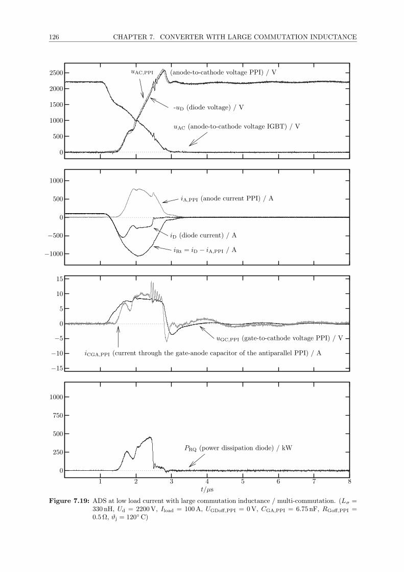
126 CHAPTER 7. CONVERTER WITH LARGE COMMUTATION INDUCTANCE
(anode-to-cathode voltage PPI) / VuAC,PPI
uAC (anode-to-cathode voltage IGBT) / V
-uD (diode voltage) / V
2500
2000
1500
1000
500
0
iRt = iD − iA,PPI / A
iA,PPI (anode current PPI) / A
iD (diode current) / A
1000
500
0
−500
−1000
iCGA,PPI (current through the gate-anode capacitor of the antiparallel PPI) / A
uGC,PPI (gate-to-cathode voltage PPI) / V
15
10
5
0
−5
−10
−15
PRQ (power dissipation diode) / kW
t/µs87654321
1000
750
500
250
0
Figure 7.19: ADS at low load current with large commutation inductance / multi-commutation. (Lσ =330 nH, Ud = 2200V, Iload = 100A, UGDoff,PPI = 0V, CGA,PPI = 6.75 nF, RGoff,PPI =0.5Ω, ϑj = 120 C)
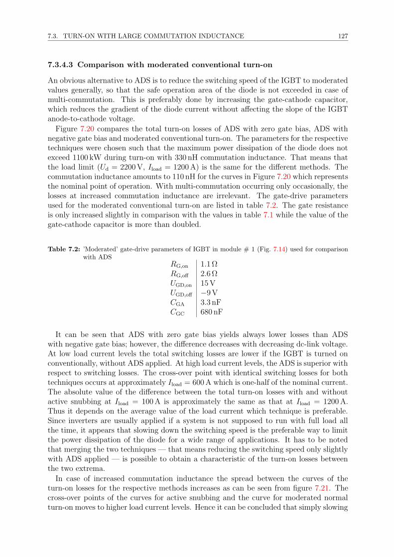
7.3. TURN-ON WITH LARGE COMMUTATION INDUCTANCE 127
7.3.4.3 Comparison with moderated conventional turn-on
An obvious alternative to ADS is to reduce the switching speed of the IGBT to moderatedvalues generally, so that the safe operation area of the diode is not exceeded in case ofmulti-commutation. This is preferably done by increasing the gate-cathode capacitor,which reduces the gradient of the diode current without affecting the slope of the IGBTanode-to-cathode voltage.
Figure 7.20 compares the total turn-on losses of ADS with zero gate bias, ADS withnegative gate bias and moderated conventional turn-on. The parameters for the respectivetechniques were chosen such that the maximum power dissipation of the diode does notexceed 1100 kW during turn-on with 330 nH commutation inductance. That means thatthe load limit (Ud = 2200 V, Iload = 1200 A) is the same for the different methods. Thecommutation inductance amounts to 110 nH for the curves in Figure 7.20 which representsthe nominal point of operation. With multi-commutation occurring only occasionally, thelosses at increased commutation inductance are irrelevant. The gate-drive parametersused for the moderated conventional turn-on are listed in table 7.2. The gate resistanceis only increased slightly in comparison with the values in table 7.1 while the value of thegate-cathode capacitor is more than doubled.
Table 7.2: ’Moderated’ gate-drive parameters of IGBT in module # 1 (Fig. 7.14) used for comparisonwith ADS
RG,on 1.1 ΩRG,off 2.6 ΩUGD,on 15 VUGD,off −9 VCGA 3.3 nFCGC 680 nF
It can be seen that ADS with zero gate bias yields always lower losses than ADSwith negative gate bias; however, the difference decreases with decreasing dc-link voltage.At low load current levels the total switching losses are lower if the IGBT is turned onconventionally, without ADS applied. At high load current levels, the ADS is superior withrespect to switching losses. The cross-over point with identical switching losses for bothtechniques occurs at approximately Iload = 600 A which is one-half of the nominal current.The absolute value of the difference between the total turn-on losses with and withoutactive snubbing at Iload = 100 A is approximately the same as that at Iload = 1200 A.Thus it depends on the average value of the load current which technique is preferable.Since inverters are usually applied if a system is not supposed to run with full load allthe time, it appears that slowing down the switching speed is the preferable way to limitthe power dissipation of the diode for a wide range of applications. It has to be notedthat merging the two techniques — that means reducing the switching speed only slightlywith ADS applied — is possible to obtain a characteristic of the turn-on losses betweenthe two extrema.
In case of increased commutation inductance the spread between the curves of theturn-on losses for the respective methods increases as can be seen from figure 7.21. Thecross-over points of the curves for active snubbing and the curve for moderated normalturn-on moves to higher load current levels. Hence it can be concluded that simply slowing

128 CHAPTER 7. CONVERTER WITH LARGE COMMUTATION INDUCTANCE
down the switching speed is preferable to ADS if the commutation inductance is large ingeneral.
The figures 7.22 and 7.23 show the single device losses in the nominal point of oper-ation (Lσ = 110 nH) for turn-on with ADS (fig. 7.22) and for moderated conventionalturn-on (fig. 7.23). Remarkably the diode loss energy remains unchanged, which meansthat the relative strain of the IGBT changes dependent on the technique. Compared toconventional switching, the relative strain of the IGBT with active snubbing employed ishigher at low load current levels while it is lower at high load currents.
The cost for multi-commutation is illustrated in figure A.14. If multi-commutation canbe excluded definitively, the IGBT can be turned on faster which yields lower turn-onlosses. The switching speed in the nominal point of operation has to be slowed down ifmulti-commutation has to be reckoned. However, the total cost can only be calculatedfor a specific load profile.

7.3. TURN-ON WITH LARGE COMMUTATION INDUCTANCE 129
moderated conventional
negative static gate bias
zero static gate bias
Total turn-on losses at 2200 V dc-link voltageW
on/
Jper
puls
e
7
6
5
4
3
2
1
0
moderated conventional
negative static gate bias
zero static gate bias
Total turn-on losses at 1800 V dc-link voltage
Won/
Jper
puls
e
7
6
5
4
3
2
1
0
moderated conventional
negative static gate bias
zero static gate bias
Total turn-on losses at 1500 V dc-link voltage
Iload/A
Won/
Jper
puls
e
120010008006004002000
7
6
5
4
3
2
1
0
Figure 7.20: Total turn-on losses in the nominal point of operation (Lσ = 110 nH). Comparison betweenactive snubbing with zero static gate bias, active snubbing with negative static gate bias,and moderated conventional turn-on; ϑj = 120 C.

130 CHAPTER 7. CONVERTER WITH LARGE COMMUTATION INDUCTANCE
moderated conventional
negative static gate bias
zero static gate bias
Total turn-on losses at 2200 V dc-link voltageW
on/
Jper
puls
e
7
6
5
4
3
2
1
0
moderated conventional
negative static gate bias
zero static gate bias
Total turn-on losses at 1800 V dc-link voltage
Won/
Jper
puls
e
7
6
5
4
3
2
1
0
moderated conventional
negative static gate bias
zero static gate bias
Total turn-on losses at 1500 V dc-link voltage
Iload/A
Won/
Jper
puls
e
120010008006004002000
7
6
5
4
3
2
1
0
Figure 7.21: Total turn-on losses in with increases commutation inductance (Lσ = 330 nH / multi-commutation). Comparison between active snubbing with zero static gate bias, activesnubbing with negative static gate bias, and moderated conventional turn-on; ϑj = 120 C.
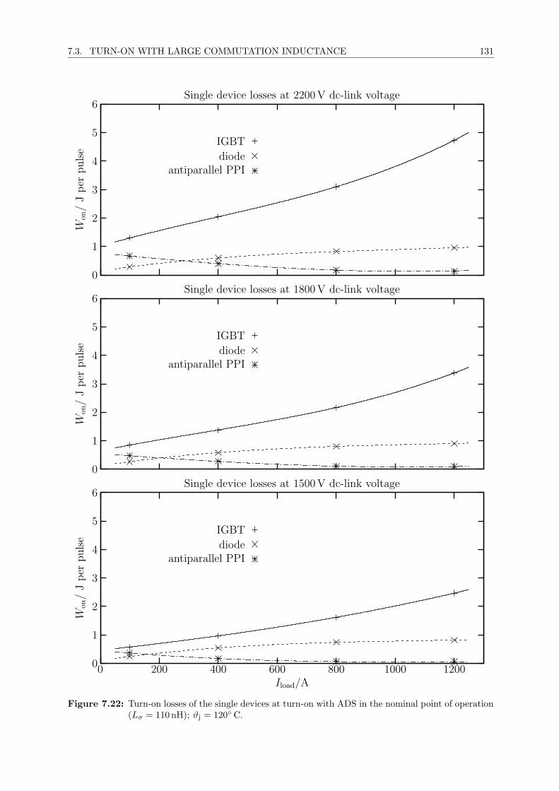
7.3. TURN-ON WITH LARGE COMMUTATION INDUCTANCE 131
antiparallel PPIdiode
IGBT
Single device losses at 2200 V dc-link voltage
Won/
Jper
puls
e
6
5
4
3
2
1
0
antiparallel PPIdiode
IGBT
Single device losses at 1800 V dc-link voltage
Won/
Jper
puls
e
6
5
4
3
2
1
0
antiparallel PPIdiode
IGBT
Single device losses at 1500 V dc-link voltage
Iload/A
Won/
Jper
puls
e
120010008006004002000
6
5
4
3
2
1
0
Figure 7.22: Turn-on losses of the single devices at turn-on with ADS in the nominal point of operation(Lσ = 110 nH); ϑj = 120 C.

132 CHAPTER 7. CONVERTER WITH LARGE COMMUTATION INDUCTANCE
antiparallel PPIdiode
IGBT
Single device losses at 2200 V dc-link voltage
Won/
Jper
puls
e
6
5
4
3
2
1
0
antiparallel PPIdiode
IGBT
Single device losses at 1800 V dc-link voltage
Won/
Jper
puls
e
6
5
4
3
2
1
0
antiparallel PPIdiode
IGBT
Single device losses at 1500 V dc-link voltage
Iload/A
Won/
Jper
puls
e
120010008006004002000
6
5
4
3
2
1
0
Figure 7.23: Turn-on losses of the single devices in the nominal point of operation (Lσ = 110 nH),moderated conventional switching; ϑj = 120 C

7.3. TURN-ON WITH LARGE COMMUTATION INDUCTANCE 133
7.3.5 Conclusion
It has been shown that an active diode snubbing (ADS) can be provided by turning onthe antiparallel IGBT during the commutation. The active snubbing allows to limit thepeak power dissipation of the diode during the reverse recovery in case of an increasedcommutation inductance. A du/dt-feedback by means of a capacitor connected betweenthe anode and the gate of the antiparallel IGBT can be employed to activate ADS ifthe gradient of the diode voltage exceeds a critical value. The gradient of the diodevoltage increases with increasing commutation inductance so that the intensity of ADSis adapted automatically. This is of interest for large inverter systems at a common dclink, where the effective commutation inductance can increase occasionally due to multi-commutation. The ADS also acts on the IGBT turning on, because the increased totalreverse current slows down the decay of the anode-to-cathode voltage. This supports the’commutation’ of the reverse current.
The maximal slope of the diode voltage imposed by the active snubbing is determinedby the allowable peak-power dissipation for the maximal commutation inductance to beexpected. This diode voltage slope is less steep than the ’intrinsic’ rate of rise of the diodevoltage at nominal commutation inductance. Hence the switching speed is reduced, too,if no multi-commutation occurs, which increases the turn-on losses compared to a casewhere multi-commutation can be excluded.
Alternatively, the IGBT can be turned on slower. It was shown that this option ispreferable at low load current levels while ADS yields lower losses at high load currentlevels. Thus it depends on the load profile which method is more beneficial: Slowingdown the switching speed is to be preferred regarding turn-on losses if the commutationinductance is large in general.
To design an ADS it is necessary to measure the currents of the diode and the an-tiparallel IGBT independently which is a challenge in high-voltage power modules. Theexperimental approach used in this work avoids that problem, but suffers from increasedstray inductance which retards the relief of the diode. However, it turned out at last thatthis is not a disadvantage, since the rate of rise of the diode voltage would be reduced un-necessarily at the beginning of the diode-voltage ramp if a ’perfect’ ADS were available.Thus delaying the onset of ADS reduces switching losses since the curve of the powerdissipation versus time takes a more rectangular shape. In consequence, no better resultsare to be expected if the IGBT in the same module as the diode is used. It has to bepointed out that ADS yields a (more or less) constant diode-voltage slope while actuallya control of the power dissipation of the diode would be desired.

134

135
8 Summary
A new description of IGBT switching transients is suggested which focuses on the com-mutation voltage as the fundamental quantity for all switching processes. The analysisof the switching waveforms is based on a control-scheme representation of the IGBTwhich covers mechanisms that are hardly describable with an electric equivalent circuit,such as the anode-current to gate-voltage feedback, the impact of mobile carriers in thedepletion layer, and the dynamics of the base resistance. Using this IGBT model, theparallel operation of IGBTs and the switching with enlarged commutation inductance areinvestigated.
The switching behaviour of IGBTs in parallel connections is studied with special em-phasis on dynamic current redistributions caused by a spread in the device characteristics.Simulations suggest that an uneven current distribution in the static case are predom-inantly caused by deviations in the bipolar section of the IGBT. It is shown that aninhomogeneous decay of the base resistances at turn-on leads to current redistributionsbetween parallelled IGBTs during the anode-current rise.
At turn-off, the total current is redistributed among parallel IGBTs at the beginningof the plateau in the gate-to-cathode voltage waveform if the characteristics of the in-herent MOSFETs diverge. In contrast, deviating bipolar sections account for currentredistributions during the rapid rise of the anode-to-cathode voltage.
In case of an enlarged commutation inductance, as typically encountered in large con-verter systems with simultaneously switching pairs of arms (multi-commutation), themaximum anode-to-cathode voltage of the IGBTs and the admissible power dissipationof the diodes have to be limited. It is shown, that the switching speed of ’field-stop’ IG-BTs has to be reduced significantly, e.g. by a zener-like feedback of the anode-to-cathodevoltage to the gate-circuit, to enable a protection against destructive overvoltages. Thisincreases the turn-off losses which for the device under test become comparable to thoseof older device generations in case of an enlarged commutation inductance.
For the protection of the diode during turn-on of the IGBT, ’Active Diode Snubbing ’(ADS) by means of the antiparallel IGBT is examined as a new technique. With respect toturn-on losses, the result is that ADS is equivalent to a general reduction of the switchingspeed if the commutation inductance is only enlarged occasionally, e.g. due to multi-commutation. However, slowing down the switching speed yields lower losses and is thuspreferable if the commutation inductance is large in general.

136

137
A Additional measurements andsimulations

138 APPENDIX A. ADDITIONAL MEASUREMENTS AND SIMULATIONS
single chip anode currents iAν/A
150
100
50
0
base resistances Rbν/Ω
3
2
1
0
gate-to-cathode voltages uGCν/V
14
13
12
11
10
9
8
7
6
5
gate-to-cathode voltage uGC × 100/V
anode-to-cathode voltage uAC/V
sum of single-chip currents iAΣ × 2/A
t/µs20181614121086420
1500
1000
500
0
Figure A.1: Redistributions of the anode current due to decay of the base resistances with differentgradients. Simulation of turn-on of four parallelled IGBTs operated with a McMurraysnubber. The oxide thicknesses of the IGBTs differ by 2.5%; all other parameters areidentical.

139
single chip anode currents iAν/A
150
100
50
0
base resistances Rbν/Ω
3
2
1
0
gate-to-cathode voltages uGCν/V
14
13
12
11
10
9
8
7
6
5
gate-to-cathode voltage uGC × 100/V
anode-to-cathode voltage uAC/V
sum of single-chip currents iAΣ × 2/A
t/µs20181614121086420
1500
1000
500
0
Figure A.2: Redistributions of the anode current due to decay of the base resistances with differentgradients. Simulation of turn-on of four parallelled IGBTs operated with a McMurraysnubber. Except the base resistance, all parameters of the IGBTs are identical.

140 APPENDIX A. ADDITIONAL MEASUREMENTS AND SIMULATIONS
single chip anode currents iAν/A
150
100
50
0
base resistances Rbν/Ω
3
2
1
0
gate-to-cathode voltages uGCν/V
14
13
12
11
10
9
8
7
6
5
gate-to-cathode voltage uGC × 100/V
anode-to-cathode voltage uAC/V
sum of single-chip currents iAΣ × 2/A
t/µs20181614121086420
1500
1000
500
0
Figure A.3: Redistributions of the anode current due to decay of the base resistances with differentgradients. Simulation of turn-on of four parallelled IGBTs operated with a McMurraysnubber. The current gains of the inherent pnp-transistors of the IGBTs differ by 30%. Allother parameters are identical.

141
anode current iA/A
anode-to-cathode voltage uAC/V
3000
2500
2000
1500
1000
500
0
diode voltage uD/V
diode current iD/A
2000
1500
1000
500
0
gate current iG/A
voltage uGC/Vgate-to-cathode
t/µs6543210
15
10
5
0
-5
-10
Figure A.4: Turn-off of a ’field-stop’ IGBT (FZ1200R33KL2, Eupec) with increased commutation in-ductance. The rise of the anode-to-cathode voltage tends to come to a standstill beforethe final rise. This eliminates the negative feedback through the gate-anode capacitor sothat the gate-to-cathode voltage decays. (Lσ = 500 nH, RG,off = 2.5Ω, CGC = 0nF,Ud = 1.5 kV, Iload = 500A, ϑj = 20 C).

142 APPENDIX A. ADDITIONAL MEASUREMENTS AND SIMULATIONS
anode current iA/A
voltage uAC/Vanode-to-cathode
3000
2500
2000
1500
1000
500
0
diode voltage uD/V
diode current iD/A
2000
1500
1000
500
0
gate current iG/A
voltage uGC/Vgate-to-cathode
t/µs1086420
15
10
5
0
-5
-10
Figure A.5: Turn-off of a ’field-stop’ IGBT (FZ1200R33KL2, Eupec) with increased commutationinductance (Lσ = 330 nH, RG,off = 2.5Ω, CGC = 0nF, Ud = 2.2 kV, Iload = 200A,ϑj = 120 C).

143
anode current iA/A
voltage uAC/Vanode-to-cathode
3000
2500
2000
1500
1000
500
0
diode voltage uD/V
diode current iD/A
2000
1500
1000
500
0
gate current iG/A
voltage uGC/Vgate-to-cathode
t/µs1086420
15
10
5
0
-5
-10
Figure A.6: Turn-off of a NPT IGBT (FZ1200R33KF1, Eupec) with increased commutation induc-tance (Lσ = 330 nH, RG,off = 2.5Ω, CGC = 0nF, Ud = 2.2 kV, Iload = 200A, ϑj = 120 C).

144 APPENDIX A. ADDITIONAL MEASUREMENTS AND SIMULATIONS
Lσ = 150 nH without active clamping
Lσ = 150 nH with active clamping
Lσ = 330 nH with active clamping
FZ1200R33KL2: Turn-off losses at 2200 V dc-link voltage
W/W
s
4
3.5
3
2.5
2
1.5
1
0.5
0
Lσ = 150 nH without active clamping
Lσ = 150 nH with active clamping
Lσ = 330 nH with active clamping
FZ1200R33KL2: Turn-off losses at 1800 V dc-link voltage
W/W
s
4
3.5
3
2.5
2
1.5
1
0.5
0
Lσ = 150 nH without active clamping
Lσ = 150 nH with active clamping
Lσ = 330 nH with active clamping
FZ1200R33KL2: Turn-off losses at 1500 V dc-link voltage
Iload/A
W/W
s
120010008006004002000
4
3.5
3
2.5
2
1.5
1
0.5
0
Figure A.7: Turn-off losses of a ’field-stop’ IGBT (FZ1200R33KL2, Eupec). Comparison betweenswitching with large commutation inductance (330 nH) and active clamping, normal com-mutation inductance (110 nH) with active clamping and normal commutation inductancewithout active clamping. (RG,off = 2.5Ω, CGA = 2.5µF, 6 × 1 .5KE400A, ϑj =120 C)

145
Lσ = 150 nH without active clamping
Lσ = 150 nH with active clamping
Lσ = 330 nH with active clamping
FZ1200R33KF1: Turn-off losses at 2200 V dc-link voltage
W/W
s
4
3.5
3
2.5
2
1.5
1
0.5
0
Lσ = 150 nH without active clamping
Lσ = 150 nH with active clamping
Lσ = 330 nH with active clamping
FZ1200R33KF1: Turn-off losses at 1800 V dc-link voltage
W/W
s
4
3.5
3
2.5
2
1.5
1
0.5
0
Lσ = 150 nH without active clamping
Lσ = 150 nH with active clamping
Lσ = 330 nH with active clamping
FZ1200R33KF1: Turn-off losses at 1500 V dc-link voltage
Iload/A
W/W
s
120010008006004002000
4
3.5
3
2.5
2
1.5
1
0.5
0
Figure A.8: Turn-off losses of a NPT IGBT (FZ1200R33KF1, Eupec). Comparison between switchingwith large commutation inductance (330 nH) and active clamping, normal commutationinductance (110 nH) with active clamping and normal commutation inductance withoutactive clamping. (RG,off = 2.5Ω, CGC = 0nF, CGA = 0µF, 6 × 1 .5KE400A, ϑj = 120 C)

146 APPENDIX A. ADDITIONAL MEASUREMENTS AND SIMULATIONS
(anode-to-cath. volt. PPI) / VuAC,PPI
uAC (anode-to-cathode voltage IGBT) / V
-uD (diode voltage) / V
2500
2000
1500
1000
500
0
iRt = iD − iA,PPI / A
iA,PPI (anode current PPI) / A
iD (diode current) / A
1000
500
0
−500
−1000
iG,PPI (gate current PPI) / A
uGC,PPI (gate-to-cathode voltage PPI) / V15
10
5
0
−5
−10
−15
PRQ (power dissipation diode) / kW
t/µs87654321
1000
750
500
250
0
Figure A.9: ADS at zero load current with large commutation inductance / multi-commutation. (Lσ =330 nH, Ud = 2200V, Iload = 100A, UGDoff,PPI = −11V, CGA,PPI = 4.05 nF, RGoff,PPI =2.5Ω, ϑj = 120 C).

147
uAC,PPI (anode-to-cathode voltage PPI) / V
uAC (anode-to-cathode voltage IGBT) / V
-uD (diode voltage) / V
2500
2000
1500
1000
500
0
iRt = iD − iA,PPI / A
iA,PPI (anode current PPI) / A
iD (diode current) / A
1000
500
0
−500
−1000
iG,PPI (gate current PPI) / A
uGC,PPI (gate-to-cathode voltage PPI) / V
15
10
5
0
−5
−10
−15
PRQ (power dissipation diode) / kW
t/µs87654321
1000
500
0
Figure A.10: ADS at high load current with large commutation inductance / multi-commutation.(Lσ = 330 nH, Ud = 2200V, Iload = 1200A, UGDoff,PPI = −11V, CGA,PPI = 4.05 nF,RGoff,PPI = 2.5Ω, ϑj = 120 C).
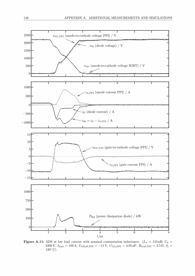
148 APPENDIX A. ADDITIONAL MEASUREMENTS AND SIMULATIONS
uAC,PPI (anode-to-cathode voltage PPI) / V
uAC (anode-to-cathode voltage IGBT) / V
-uD (diode voltage) / V
2500
2000
1500
1000
500
0
iRt = iD − iA,PPI / A
iA,PPI (anode current PPI) / A
iD (diode current) / A
1000
500
0
−500
−1000
iG,PPI (gate current PPI) / A
uGC,PPI (gate-to-cathode voltage PPI) / V
15
10
5
0
−5
−10
−15
PRQ (power dissipation diode) / kW
t/µs87654321
1000
750
500
250
0
Figure A.11: ADS at low load current with nominal commutation inductance. (Lσ = 110 nH, Ud =2200V, Iload = 100A, UGDoff,PPI = −11V, CGA,PPI = 4.05 nF, RGoff,PPI = 2.5Ω, ϑj =120 C).

149
uAC,PPI (anode-to-cathode voltage PPI) / V
uAC (anode-to-cathode voltage IGBT) / V
-uD (diode voltage) / V
2500
2000
1500
1000
500
0
iRt = iD − iA,PPI / A
iA,PPI (anode current PPI) / A
iD (diode current) / A
1000
500
0
−500
−1000
iCGA,PPI (current through the gate-anode capacitor of the antiparallel PPI) / A
uGC,PPI (gate-to-cathode voltage PPI) / V
15
10
5
0
−5
−10
−15
PRQ (power dissipation diode) / kW
t/µs87654321
1000
750
500
250
0
Figure A.12: ADS at high load current with nominal commutation inductance. ( Lσ = 110 nH, Ud =2200V, Iload = 1200A, UGDoff,PPI = 0V, CGA,PPI = 6.75 nF, RGoff,PPI = 0.5Ω, ϑj =120 C).

150 APPENDIX A. ADDITIONAL MEASUREMENTS AND SIMULATIONS
uAC,PPI (anode-to-cathode voltage PPI) / V
uAC (anode-to-cathode voltage IGBT) / V
-uD (diode voltage) / V
2500
2000
1500
1000
500
0
iRt = iD − iA,PPI / A
iA,PPI (anode current PPI) / A
iD (diode current) / A
1000
500
0
−500
−1000
iCGA,PPI (current through the gate-anode capacitor of the antiparallel PPI) / A
uGC,PPI (gate-to-cathode voltage PPI) / V
15
10
5
0
−5
−10
−15
PRQ (power dissipation diode) / kW
t/µs87654321
1000
750
500
250
0
Figure A.13: ADS at low load current with nominal commutation inductance. (Lσ = 110 nH, Ud =2200V, Iload = 100A, UGDoff,PPI = 0V, CGA,PPI = 6.75 nF, RGoff,PPI = 0.5Ω, ϑj =120 C).
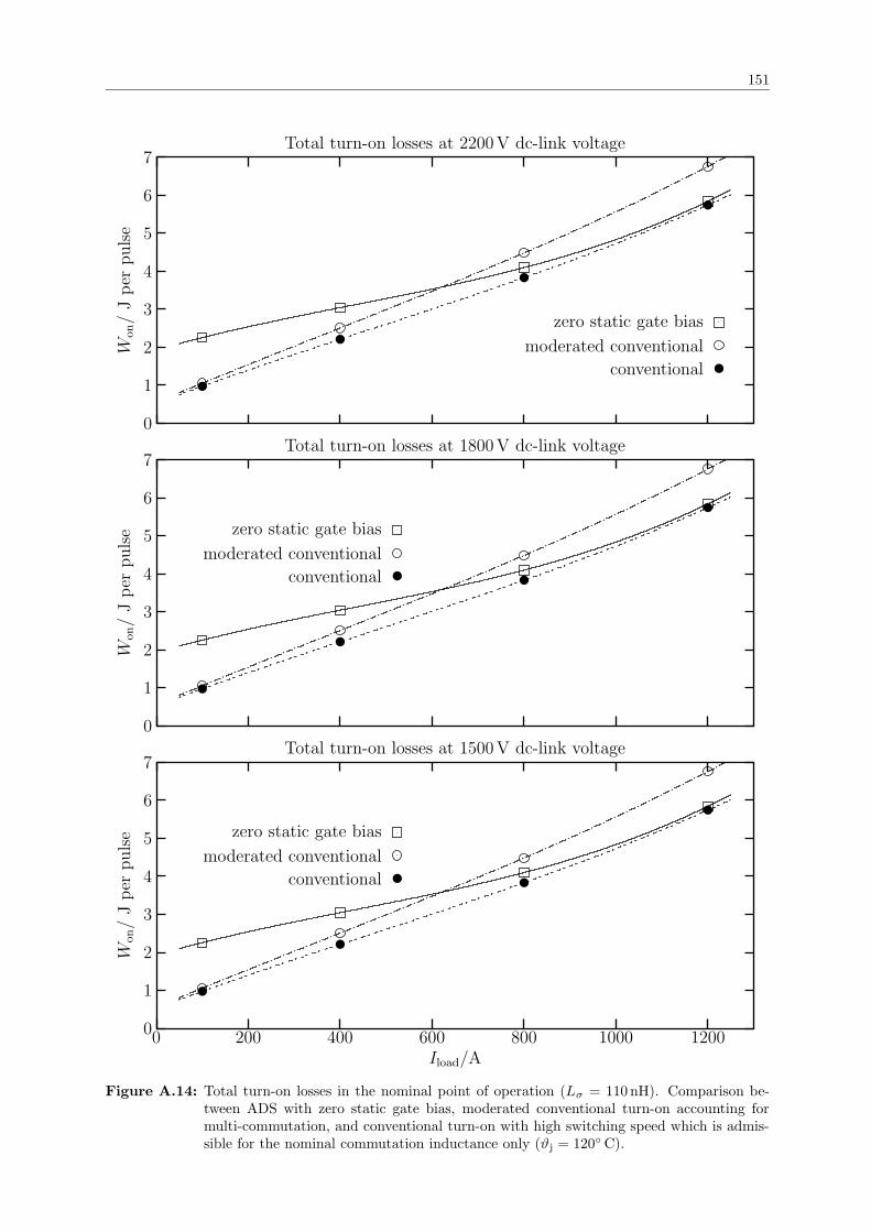
151
conventional
moderated conventional
zero static gate bias
Total turn-on losses at 2200 V dc-link voltageW
on/
Jper
puls
e
7
6
5
4
3
2
1
0
conventional
moderated conventional
zero static gate bias
Total turn-on losses at 1800 V dc-link voltage
Won/
Jper
puls
e
7
6
5
4
3
2
1
0
conventional
moderated conventional
zero static gate bias
Total turn-on losses at 1500 V dc-link voltage
Iload/A
Won/
Jper
puls
e
120010008006004002000
7
6
5
4
3
2
1
0
Figure A.14: Total turn-on losses in the nominal point of operation (Lσ = 110 nH). Comparison be-tween ADS with zero static gate bias, moderated conventional turn-on accounting formulti-commutation, and conventional turn-on with high switching speed which is admis-sible for the nominal commutation inductance only (ϑj = 120 C).

152
153
B Power-electronic measurements
B.1 Data acquisition
The use of digital storage oscilloscopes for recording waveforms of voltages and currents inpower-electronic circuits is hampered by the fact that the reference potential may have ahigh voltage with respect to ground. As far as the power supply is concerned, an isolatingtransformer can be used. However, the data acquisition is complicated, too, since the scopemust not be touched while in operation. Fortunately, most modern oscilloscopes providean interface to read out the recorded waveforms and to change settings digitally. Themost interesting option in doing so is to use an Ethernet adapter because of the low costof widely-used network components. The oscilloscopes used in this report are operatedwith remote control via Ethernet, whereas the data potential separation is provided byuse of wireless-LAN access points. The latter has the benefit of higher mobility and lowerprice compared to a solution using fibre-optic transmitters.
Using the remote control option is very beneficial since the storage capability of both theoscilloscope’s internal memory and a possibly built-in floppy-disk drive are very limitedcompared to the amount of data recorded in a single acquisition.
The communication with the oscilloscopes is managed by a set of perl [119] scriptswhich allow to set parameters and to read out the acquired waveforms. The softwareprovided by the manufacturer for the same purpose turned out to be unemployable becauseof frequent system crashes. The command strings sent to the oscilloscopes with help ofthe perl scripts are generated by an Octave [27] script which also allows the automaticadaption of the vertical resolution to the measured data: A first set of waveforms acquiredwith a low resolution is used to determine the maxima and minima. From this data set,the optimum vertical resolution is calculated for the final measurement.
The oscilloscopes LeCroy LT344 are triggered via a fibre-optic transmitter. The sup-ply voltage for the receiver is taken from the power-supply output at the front panel whichis originally provided for proprietary active voltage probes. The trigger signal is generatedby the pulse generator that controls the power-electronic switches.
B.2 Measures against electromagnetic interferences
B.2.1 Sources of interference
Switched currents and voltages of large magnitude in power-electronic circuits can easilydisturb measurements. Generally speaking the energy of interference can be inserted intothe measurement circuit by
1. conductive coupling (via common impedance),
2. electrostatic (capacitive) coupling ,

154 APPENDIX B. POWER-ELECTRONIC MEASUREMENTS
3. inductive coupling via mutual inductance,
4. electromagnetic radiation,
5. a jumping reference potential.
The discussions of capacitive and inductive coupling assume that electric and magneticfields are independent from each other as it is true in the near field (r << λ/2π). Incontrast electromagnetic radiation (coupled electric and magnetic fields) occurs in the farfield (r >> λ/2π) of the radiating structure. With frequency components not exceeding200 MHz (analogue bandwidth of the oscilloscopes), thus λ > 1.5 m, disturbances due toelectromagnetic radiation are negligible. Please note that frequency components of powerelectronic waveforms usually do not exceed 15 MHz.
B.2.2 Common impedance
Except for the shunt resistor the function of which is based on common impedance,current paths common to measurement circuit and load circuit have to be strictly avoidedfor oscilloscope measurements. The ground leads of all measurement connections mustbe connected to the identical potential, i.e. no current must flow between the points ofcontact. Otherwise voltage drops between the points of contact lead to currents throughthe shields of the measurement connections which at the best corrupt the measurementsdue to voltage drops at the impedances of the shields, or which at the worst lead to thedestruction of probes and oscilloscope.
B.2.3 Capacitive coupling (du/dt-interference)
Figure B.1 shows the representation of a coaxial cable as it is common for current andvoltage probes, that is connected to an oscilloscope with an input impedance Zi. Zc isthe impedance of the centre conductor and Zs the impedance of the shield, C1 representsthe capacitance between centre conductor and shield.
PSfrag replacements
C1
Ccoup
uq
Zs
Zc
Zi
scope
Figure B.1: Capacitive shielding
A parasitic coupling capacitance exists between the shield and other surfaces, whichis labelled Ccoup in figure B.1. Whenever the voltage uq between the shield and the

B.2. MEASURES AGAINST ELECTROMAGNETIC INTERFERENCES 155
surrounding surfaces changes, a displacement current through Ccoup occurs that is for thegreatest part drained to ground if the impedance Zs is sufficiently small. Nonetheless thisdisplacement current causes a voltage drop at Zs which causes a current through C1, Zc
and Zi that deteriorates the measurement due to the voltage drop at the input impedanceZi of the oscilloscope. It is important to note that the shield of a coaxial cable is not aFaraday cage since the centre conductor is connected to ground via Zi. For that reasonit is essential that a capacitive shield is connected to ground so that the displacementcurrent of Ccoup is shorted to ground via Zs << Zi + Zc. Zs, which is referred to astransfer impedance, is an important attribute of a coaxial cable.
Measures against capacitive coupling are: [112] [26]
• routing of the measurement leads with maximum distance to the power circuit toreduce the coupling capacitance,
• limiting the bend radius of coaxial cable to less than ten times the nominal diameterto avoid apertures in the braiding [112],
• providing an additional shield to prevent the displacement current through the par-asitic capacitances from flowing in the shield of the coaxial cable that is part of themeasuring circuit, so that the voltage drop at Zs is avoided.
B.2.4 Inductive coupling (di/dt-interference)
Any loop span by the measuring leads has a mutual inductance M with the load circuit. Achange of the magnetic flux associated with currents in the load circuit that is penetratingthese loops induces voltages on the measuring leads which may corrupt the measurements.
The most important measure against inductive coupling therefore is to minimise thesurface bounded by the measuring leads. This means to run all leads connected to theoscilloscope as close to each other as possible. In addition, the instrument leads are againseparated as far as possible from the conductors of the power circuit. Crossings betweenpower-circuit conductors and the measuring circuit, if inevitable, have to be provided ina right angle to minimise coupling [112].
Especially the ground leads of voltage probes can cause serious problems if they spanloops enclosing unnecessary large areas nearby the power-electronic circuit. If voltages ofsmall magnitude like gate-to-cathode voltages of power devices have to be measured, theuse of sockets which minimise the area enclosed by the ground connection is mandatory(Fig. B.4). If the ground lead of the voltage probe has to be used, its distance to the testprod must be minimal.
The inductive coupling with the load circuit makes it virtually infeasible to preciselymeasure voltages in the order of magnitude of few volts in distances of more than severalcentimetres from the reference potential because of the area that would be encompassedby the ground lead otherwise.
B.2.5 Jumping reference potential
As mentioned in Section B.1 the oscilloscopes must be connected to the mains via anisolating transformer if the reference potential of the measurement is not the ground.However, a transformer can only decouple the oscilloscopes from dc- and low-frequency

156 APPENDIX B. POWER-ELECTRONIC MEASUREMENTS
voltages, while the parasitic capacitances of the windings and of the housing of the oscil-loscope still provide a high-frequency coupling to ground.
If the reference potential of the measurement is ’jumping’ with respect to ground, whichis likely to be encountered in switch-mode converters due to the steep gradients of thedevice voltages and because of the voltage drop at the stray inductance of the busbars,the displacement current of the parasitic capacitances to ground of the oscilloscope andits isolating transformer will flow through the ground leads of the measuring lines, as faras no countermeasures are taken. This current will cause voltage drops at the impedanceof the shields Zs which deteriorates the measurement. The error increases with magnitudeof the excursion of the potential and with frequency, because of the decreasing impedanceof the capacitance.
Hence, it is essential for high-precision power-electronic measurements to choose thereference potential as constant as possible. The best choice is usually a point as close aspossible to the connection of a large capacitor, e.g. the dc-link capacitor in a voltage-source inverter. Definitively unsuitable as reference are points with jumping potential likethe load connection of an inverter leg.
It is common practice to avoid shield currents by linking oscilloscope ’ground’ to thereference potential with an extra cable [109]. For minimum impedance at high frequenciesthis cable should be a cord of parallel, not braided wires. Especially a braided cable shieldis not suitable [111]. To ensure that the displacement current is flowing exclusively throughthe extra ground cable, common-mode chokes formed by winding the coaxial cables on aferrite core are provided for the measurement connections as depicted in Figure B.2. Thisis referred to as ’bypass technique’ [45][103].
bypassPSfrag replacements
C1
C1
Cg
uq
uq
Zs
Zc
Zi
idispl
idisplscope
Figure B.2: Bypass technique to suppress displacement currents on the screens of the measuring leads.
The common-mode choke adds a series impedance to the braided shield of the measuringline. This prevents the drain of the displacement currents due to capacitive coupling andthus eliminates the capacitive screening effect of the coaxial cable (Sect. B.2.3). However,in the ideal case the voltage drop at the choke impedance in the screen ideally induces acorresponding voltage in the centre conductor due to the magnetic coupling. Hence, thevoltage at the coupling capacitance C1 between centre conductor and shield is nearly zeroif the impedance of the common-mode choke is much larger than the transfer impedanceof the shield Zs. It will be shown in subsection B.3.3 that this theory does not apply inpractice.

B.3. IMPROVING POWER-ELECTRONIC MEASUREMENTS 157
B.3 Improving power-electronic measurements
B.3.1 Motivation
The precise measurement of small signals in power-electronic circuits is a challenging task.Examples of such signals are output voltages of Rogowski coils, gate-to-cathode voltagesof IGBTs and voltages in the circuits of the gate drive. Extensive measurements havebeen performed to detect and distinguish the relevant causes for interferences of powerelectronic measurements and to evaluate measures against them [12]. The results aresummarised in the following subsections.
B.3.2 Test setup
The power-electronic circuit producing the interferences studied here is a step-down con-verter using two power modules FZ1200R33KF1 (Eupec) with the switch on the ’low-side’. The measurements were taken with two LeCroy LT344 oscilloscopes, which areelectrically isolated from ground and from each other by two isolating transformers. Oneoscilloscope is used to measure the anode-to-cathode voltage and the anode current ofthe switch. The other oscilloscope is used to measure solely the voltage of a shortedTektronix P6139A 1:10 voltage probe that is connected to the dc-link busbar. Sincethe voltage measured with a shorted voltage probe should be zero, any voltage measuredin this configuration is caused by interference. The separate oscilloscope is provided forthe shorted voltage probe to exclude any interference caused by the other probes. FigureB.3 illustrates the setup. The oscilloscope and the probes measuring the anode currentand the anode-to-cathode voltage of the IGBT are omitted in the figure B.3 for clarity.The three major sources of interference are:
PSfrag replacements
anodecathode
gate
scope
iA
uAC
uGC
Ud
uD
uLσ
Iload = const
iA
iDiG
RG
Lσ
uGD
H
Cg,dc−link
Cg,scope
Ccoup
Ψ = M · iA
Lload
Iload
Figure B.3: Standard setup for power-electronic measurements. (Ud = 2200V, Iload = 1200A)

158 APPENDIX B. POWER-ELECTRONIC MEASUREMENTS
1. Magnetic flux Ψ = M · iA associated with the anode current iA of the IGBT by themutual inductance M is penetrating the loop that is shorting the voltage probe.When the current iA and thus the flux Ψ changes, an error voltage is induced. Tominimise the area span by the loop that is shorting the prod to the shielding ofthe coaxial cable of the voltage probe, a special socket is employed (Figure B.4).Although an even improved short with less span area and consequently smallermutual inductance is feasible, the socket is used which is also utilised for the othermeasurements with this voltage probe presented in this work.
2. The coupling capacitance Ccoup symbolises the capacitive coupling between the volt-age probe and the surrounding surfaces. Among these, the load connection (IGBTanode) is most relevant because of the high potential difference and the fast changein potential when the IGBT switches. During a transient of the anode-to-cathodevoltage of the IGBT, a displacement current through Ccoup afflicts the measurementas discussed in Subsection B.2.3.
3. The reference potential jumps with respect to ground during the current transientdue to the voltage drop uLσ at the stray inductance Lσ of the dc-link busbar onthe low-side. A change of uLσ causes a displacement current through the groundcapacitance of the dc-link, Cg,dc−link, and the ground capacitance of the oscilloscope,Cg,scope. This current flows through the screen of the coaxial cable of the voltageprobe where it causes a voltage drop that corrupts the measurement without othermeasures taken.
One motivation for the measurements presented in this Section was to examine thefeasibility of the measurement of single-chip currents inside IGBT modules with Rogowskicoils. To that end the PCB emulation of the ceramic substrate inside an IGBT moduleshown in Figure B.4 was built. The aluminium bond wires are substituted by insulatedcopper wires of the same diameter. The PCB representation of the ceramic substrate isinserted electrically into the dc-link busbar on the low-side.
B.3.3 Measurements
Figure B.5 shows the waveform of the error voltage uVP measured with the shorted voltageprobe that is connected to the dc-link potential during turn-off of the IGBT (Figure B.3).In addition the waveforms of the anode-to-cathode voltage uAC and the anode current iAof the IGBT are plotted. It can be seen that the rise of the anode-to-cathode voltageuAC afflicts slightly the measured voltage uVP due to the coupling capacitance Ccoup inthe period (4.0 µs...4.7 µs). When the anode current iA starts to fall, a much strongerinterference occurs which is caused by the inductive coupling because of the changingcurrent and by the changing reference potential because of the voltage drop at the strayinductance Lσ. An oscillation with rather short period (≈ 200 ns) develops during theanode-current ramp which decays within ≈ 2 µs. After the switching transients a lowfrequency oscillation with a period of several µs is apparent in the waveform of uVP.While the interference due to capacitive coupling can be clearly assigned, the influenceof the inductive coupling and the jumping reference potential cannot be distinguished inthis measurement.

B.3. IMPROVING POWER-ELECTRONIC MEASUREMENTS 159
Figure B.4: Shorted voltage probe connected to the PCB emulation of a ceramic substrate inside anIGBT module.
The waveform of the error voltage recorded with a voltage probe equipped with acommon-mode choke (Subsection B.2.5) that is connected to the dc-link potential witha parallel wire as bypass is depicted in figure B.6. This is the ’state-of-the-art’ setupfor power-electronic measurements [109]. Both the high-frequency oscillation and thelow-frequency oscillation are suppressed in this configuration. Compared to Figure B.5the peak error voltage is reduced from 194 mV to 144 mV by means of the common-mode choke in combination with the parallel wire connected to the reference potential onboth sides. However, the waveform of the error voltage shows a slowly decaying offsetafter the switching of the IGBT which increases the mean error voltage over the wholemeasuring period from 11 mV without common mode choke to 15 mV. This is extremelydisadvantageous for the measurement of Rogowski-coil signals since the offset is time-integrated when the current is calculated from the coil signal. The r.m.s over the wholerecording time of the error voltage decreases from 29 mV without common mode choketo 26 mV.
To look deeper into the effect of the jumping reference potential, the shorted voltageprobe is now connected to the anode of the IGBT of the step-down converter. This setupis illustrated in Figure B.7. It could be seen from Figure B.5 that capacitive couplinghas a negligible impact. Nevertheless, for completeness Ccoup is included in figure B.7as a coupling capacitance between the voltage probe and the dc-link busbar of the ’low-side’. The dc-link voltage amounts to 100 V for this experiment which is in the orderof magnitude of the voltage at the stray inductance in the dc-link busbar that occursin the experiments presented earlier in this section. Figure B.8 shows the waveforms ofthe anode-to-cathode voltage of the IGBT and the error voltage uVP of a plain shortedvoltage probe that is connected to the anode of the IGBT according to Figure B.7. Theanode current of the IGBT is zero and therefore not plotted here. It can be seen that

160 APPENDIX B. POWER-ELECTRONIC MEASUREMENTS
uVP = 194 mVuVP = 11 mVuVP,rms = 29 mVerror voltage uVP · 10 / mV
anode-to-cathode voltage uAC/ Vanode current iA/ A
t/µs109876543210
3000
2500
2000
1500
1000
500
0
−500
PSfrag replacements
scopeH
Ψ = M · iA
iA
uACuLσ
idispl
Cgr,dc−link
Cgr,scope
Ccoup
9MΩ
C1
Zs
Zc
Zi
Lload
Iload
Figure B.5: Error voltage of a shorted voltage probe that is connected to the dc-link busbar.
uVP = 144 mVuVP = 15 mVuVP,rms = 26 mVerror voltage uVP · 10 / mV
anode-to-cathode voltage uAC/ Vanode current iA/ A
t/µs109876543210
3000
2500
2000
1500
1000
500
0
−500
PSfrag replacements
scopeH
Ψ = M · iA
iA
uACuLσ
idispl
Cgr,dc−link
Cgr,scope
Ccoup
9MΩ
C1
Zs
Zc
Zi
Figure B.6: Error voltage of a shorted voltage probe equipped with a common mode choke that isconnected to the dc-link busbar with a parallel wire.

B.3. IMPROVING POWER-ELECTRONIC MEASUREMENTS 161
PSfrag replacements
anodecathode
gate
scope
iA
uAC
uGC
Ud
uD
uLσ
Iload = 0
iA = 0
iDiG
RG
Lσ
uGD
H
Cgr,dc−link
Cgr,scope
Cc
Ψ = M · iA
Lload
Iload = 0
Figure B.7: Setup for the examination of measurement errors introduced by a jumping reference po-tential. (Ud = 100V, Iload = 0A)
both the high-frequency oscillation and the low-frequency oscillation observed in figureB.5 are excited by the jumping reference potential. The offset in uVP after the switchingis caused by the jumping reference potential, too.
Applying the bypass technique in this configuration suppresses the oscillations as canbe seen from Figure B.9. This effect is already known from figure B.6. However, theoffset after the switching of the IGBT remains. The reason for this offset is a capacitivecoupling between the coaxial cable of the voltage probe and the wire used for the bypass.Because the greatest part of the voltage between the reference potential and ground dropsat the common-mode choke, the bypass wire has a substantial potential with respect tothe coaxial cable of the voltage probe. As stated in Subsection B.2.5, the common-modechoke eliminates the screening effect of the braided shield of the coaxial cable. Obviouslythe capacitance C1 between shield and centre conductor of the coaxial cable is loadedby a displacement current that is not suppressed by the common-mode choke, whichtheoretically should equalise the currents of centre conductor and shield of the coaxialcable. This is not astonishing, since a common mode choke built by winding the coaxialcable on a magnetic core is by far not an ideal transformer.
Figure B.10 shows the error-voltage waveform if an additional screen is provided for thecoaxial cable of the voltage probe, with all other parameters unchanged from Figure B.9.The shield is connected to the reference potential at the oscilloscope only; its capacitivescreening eliminates the step in the error-voltage waveform after the switching of theIGBT completely. Hence it has to be concluded that for highly precise measurements,the bypass technique has to be completed by an additional capacitive shielding for thecoaxial cable of the probe.
In Figure B.11 the error voltage waveform for the setup and the load condition (turn-offat Ud = 2200 V, Iload = 1200 A) sketched in figure B.3 is shown if the bypass techniqueis combined with an additional capacitive screening. The mean value of the error voltage

162 APPENDIX B. POWER-ELECTRONIC MEASUREMENTS
is reduced to 6 mV compared to 15 mV with plain shielding. The peak error voltage isreduced by 33 mV to 111 mV, while the root mean square value is reduced from 26 mV to17 mV. The remaining error is almost exclusively caused by inductive coupling. Furtheroptimisation is impossible without changing the design of the voltage probe and its socketconnector which is shorting the prod.
uVP = 36 mV
uVP = 18 mV
uVP,rms = 22 mV
error voltage uVP/ mV
anode-to-cathode voltage uAC/ V
t/µs109876543210
100
80
60
40
20
0
−20
PSfrag replacements
scope
HΨ = M · iA
iA
uAC
uLσ
idispl
Cgr,dc−link
Cgr,scope
Ccoup
9MΩ
C1
Zs
Zc
Zi
Figure B.8: Error voltage of a shorted voltage probe connected to the anode of an IGBT that is turnedon at zero load current.
B.3.4 Discussion
The measurements presented in the previous Subsection prove that the screening of acoaxial cable against capacitive coupling is greatly reduced if the bypass technique withcommon-mode choke is applied. The loss of capacitive screening for the cable itself ispartly compensated by the fact that the parallel bypass wire acts as a partial screen.However, measurements can be improved significantly if an extra capacitive screen issupplied.
The double screening especially eliminates the step in the waveform of the error voltage.This is very important for the measurement of Rogowski-coil signals since a step errorin the signal leads to a gradient in the current calculated by time integration from themeasured voltage.
The error which is remaining despite bypass technique with double screening is due toinductive coupling. As far as measurements of Rogowski-coil signals are concerned, thiserror can be accounted for by calibrating the coil in the same place where the measurementis to be performed. That way the error due to inductive coupling is credited to the mutualinductance of the coil.

B.3. IMPROVING POWER-ELECTRONIC MEASUREMENTS 163
uVP = 25 mV
uVP = 12 mV
uVP,rms = 15 mV
error voltage uVP/ mV
anode-to-cathode voltage uAC/ V
t/µs109876543210
100
80
60
40
20
0
−20
PSfrag replacements
scope
HΨ = M · iA
iA
uAC
uLσ
idispl
Cgr,dc−link
Cgr,scope
Ccoup
9MΩ
C1
Zs
Zc
Zi
Figure B.9: Error voltage of a shorted voltage probe with bypass technique applied. The probe isconnected to the anode of an IGBT that is turned on at zero load current.
uVP = 9 mV
uVP = 1 mV
uVP,rms = 2 mV
error voltage uVP/ mV
anode-to-cathode voltage uAC/ V
t/µs109876543210
100
80
60
40
20
0
−20
PSfrag replacements
scope
HΨ = M · iA
iA
uAC
uLσ
idispl
Cgr,dc−link
Cgr,scope
Ccoup
9MΩ
C1
Zs
Zc
Zi
Figure B.10: Error voltage of a shorted voltage probe with double screening and bypass techniqueapplied. The probe is connected to the anode of an IGBT that is turned on at zero loadcurrent.

164 APPENDIX B. POWER-ELECTRONIC MEASUREMENTS
uVP = 111 mV
uVP = 6 mV
uVP,rms = 17 mV
error voltage uVP/ mV
anode-to-cathode voltage uAC/ V
t/µs109876543210
100
80
60
40
20
0
−20
PSfrag replacements
scopeH
Ψ = M · iA
iA
uACuLσ
idispl
Cgr,dc−link
Cgr,scope
Ccoup
9MΩ
C1
Zs
Zc
Zi
Figure B.11: Error voltage of a shorted voltage probe equipped with double screening and bypasstechnique applied. The probe is connected to the dc-link busbar. The position of thevoltage probe and the load condition is exactly the same as for the measurements shownin figure B.5 and figure B.6.

B.4. CURRENT MEASUREMENT 165
B.4 Current measurement
B.4.1 Current probes
Current probes convert the current to be measured into a proportional voltage that canbe recorded with an oscilloscope. The most popular current probes for power electronicmeasurements are Rogowski coils [96] and high-frequency shunts.
Rogowski coils have the great advantage that they can be simply put around a conductoror a device, so that there is no (or only very little) need to modify the circuit. Sincecurrents in power electronic circuits are usually switched so that their value is zero eitherat the beginning or at the end of the measuring period, it is no drawback that Rogowskicoils cannot measure dc current portions. However, Rogowski coils are susceptible tocapacitive coupling which, dependent on the situation, can cause interferences.
High-frequency shunts are used for measurements in power electronic if the currentto be measured has a relevant dc portion or if Rogowski coils cannot be used becauseof capacitive interferences. The original layout of the power circuit has to be changedto insert a shunt. Furthermore, the shunt defines the reference potential. Hence, themeasurement of voltages is deteriorated because not exactly the actually desired potential(e.g. the cathode of a power device) can be used as reference. This does not apply if thevoltages can be measured with an extra oscilloscope or if differential amplifiers are used.However, differential amplifiers are alway less accurate than passive voltage probes.
For the measurement of the gate currents of power devices, usually neither shuntsnor a Rogowski coils are suitable. A shunt would determine the reference potential inan unfavourable fashion and it is too bulky to be positioned close to the power device.Rogowski coils for the measurement of small currents need many windings to attain asufficient output signal. But, a high number of windings increases the capacitance of thecoil which reduces the bandwidth. For that reason current transformers with a magneticcore are more suitable for the measurement of gate currents.
B.4.2 High-frequency coaxial shunt
Measuring currents in power-electronic circuits by means of the voltage drop at a shuntresistor brings about the determination of the reference potential. Furthermore, the in-sertion of the shunt into the circuit requires a change of the original geometry. Thoughthese are undesirable constraints, in some cases a shunt is favoured because of its high im-munity against electromagnetic fields, the high bandwidth and the capability to measuredc currents.
A shunt for the measurement of pulse currents with high-frequency components shouldbe purely ohmic and therefore must have both low inductance and low capacitance. In-deed, minimising inductance and capacitance of a configuration of conductors at the sametime alway results in a compromise since a low inductance requires broad conductorsmounted very close to each other, while just the opposite is needed for a low capacitance.In the frequency range of interest in power-electronic circuits (/ 15 MHz), the inductivecomponent of the shunt impedance is dominant.
If only single current pulses with durations in the order of magnitude of millisecondsare addressed, the power dissipated in the shunt is negligible, even with pulse peaks ofmore than 1 kA. In this case, cooling is not an issue and the dimensions of the shunts can

166 APPENDIX B. POWER-ELECTRONIC MEASUREMENTS
be chosen small, leading to a design with very low inductance which is superior to shuntsdesigned for high r.m.s. power-frequency currents.
Figure B.12 shows a cross-sectional drawing of the shunt in the usual double-coaxialform that has been designed, built and used in this work. This shunt is here referredto as ’Eele shunt’, referring to the Institute of Electrical Power Engineering and PowerElectronics (Elektrische Energietechnik und Leistungselektronik). The current to be
30
30
M2.3
PSfrag replacements
hollow cylinder (brass)
insulation (hard paper)
resistive hollow cylinder
PTFE core
i
i
PSfrag replacements
hollow cylinder (brass)insulation (hard paper)
resistive hollow cylinder
PTFE corei
PSfrag replacements
hollow cylinder (brass)insulation (hard paper)
resistive hollow cylinder
PTFE corei
Figure B.12: Sectional drawing and photos of the coaxial shunt (’Eele shunt’)
measured is flowing through the outer hollow cylinder made of brass from the side withthe load connections to the side with the bayonet nut connector (BNC). From therethe current is flowing back through the inner hollow cylinder made of a resistive sheet(Manganin r©). A hollow cylinder made of hard paper isolates the outer brass cylinderfrom the inner resistive cylinder. Inside the resistive cylinder, there is a core made ofpolytetrafluorethylen (PTFE) which is better known under the brand name Teflon r©. Inthe axis of the PTFE core there is an internal thread in which the second load connectoris screwed, which features a 2-mm bore acting as a socket for both the connection of the

B.4. CURRENT MEASUREMENT 167
PSfrag replacements
im(t)
ui(t)
Figure B.13: Rogowski coil
load with a plug from outside and the connection of the BNC from inside.One key-element of the design is that the resistive cylinder is only fixed at the BNC
side and that the load and the measuring contact are connected with plug-in contacts atthe other side. That way any mechanical force is kept away from the resistive cylinderwhich enhances precision.
B.4.3 Rogowski coils
B.4.3.1 Rogowski coil basics
Rogowski coils [98][44][59][96] are toroidal coils on a non-ferromagnetic core that are usedas current transducer, as depicted in Figure B.13. A change in the measured current im(t)alters the strength of the magnetic field pervading the windings of the coil. This inducesa voltage
ui(t) = M · dim(t)
dt(B.1)
Assuming an ideal coil, the current signal i∗m(t) is obtained by time-integration accordingto
i∗m(t) =1
M
∫
ui(t) · dt. (B.2)
where M is the mutual inductance of the coil and the conductor carrying the measuredcurrent. The most important benefits of Rogowski coils for measurements in power elec-tronic circuits are:
1. measurements are potential-free
2. there is no need for modifying the circuit under test for the insertion of the currentprobe since the Rogowski coil can be simply put around conductors or devices
3. the load added to the circuit under test by insertion of the current probe is negligible
4. maintenance and re-calibration are not necessary.

168 APPENDIX B. POWER-ELECTRONIC MEASUREMENTS
PSfrag replacements
im ui = M · dimdt
R L
C Rt um
Figure B.14: Equivalent circuit of a Rogowski coil with lumped impedances
B.4.3.2 Dynamic characteristic of the Rogowski coil
The output voltage of a technical Rogowski coil, um, does not equal the induced voltageui which is the product of mutual inductance M and current slope di/dt. The dynamiccharacteristic of the Rogowski coil is determined by the resistance R, the capacitance Cand the inductance L of the coil. The inductance is the mutual inductance M multipliedby the number of turns w
L = M · w (B.3)
since the flux of the coil is interlinked with all windings, while it is interlinked with onlythe single turn carrying the measured current in case of the mutual inductance. FigureB.14 shows the common equivalent circuit of a Rogowski coil with lumped impedances[96] which is derived from [21].
Oscillations between the inductance and the capacitance of the windings can occur if thecoil is excited by a change of the measured current im. Such oscillations can be suppressedby connecting a terminating resistor Rt in parallel to the coil. The current through theterminating resistor causes a component in the output voltage that is proportional tothe measured current. The smaller Rt, the more the Rogowski coil becomes a currenttransformer.
The measured current i∗m is calculated from the measures Rogowski-coil output um
according to
i∗m =1
M
∫
ui (B.4)
=1
M
(
Rt + R
Rt
·∫
um · dt + (L
Rt
+ RC) +L
Rt
) · um + LC · dum
dt
)
. (B.5)
If the resonant frequency of the Rogowski coil is considerably higher than the maximumfrequency component of the measured current, the capacitance of the coil can be neglectedfor the calculation of the current, so that equation B.5 becomes
i∗m =1
M
∫
ui (B.6)
=1
M
(
Rt + R
Rt
·∫
um · dt +L
Rt
· um
)
. (B.7)

B.4. CURRENT MEASUREMENT 169
RLC-model
RL-model
measured impedance
f/MHz
|Zcoil|/
Omega
6050403020100
2500
2000
1500
1000
500
0
Figure B.15: Impedance of the EELE Rogowski coil as function of the frequency. Below 15MHz thecoil capacitance can be neglected. The RLC-model from Figure B.14 is accurate up to40MHz.
B.4.3.3 The EELE Rogowski coil
The Rogowski coil developed and employed in this work is a double-layer coil with 15 cmdiameter which corresponds to a length of 47 cm. The diameter of the windings is 3.3 mm.For minimal parasitic capacitance between the two tape layers the turns cross in a rightangle. This is achieved by using the circumference of the core as pitch for the winding.The coil is wound on the polyvinylchlorid (PVC) insulation of a copper wire, which isremoved after manufacturing the coil. The windings are fixed on the core with clear gloss[59].
Figure B.15 shows the impedance of the EELE Rogowski coil as function of the fre-quency. The Rogowski-coil model in figure B.14 is accurate for frequencies up to 40 MHz.Below 15 MHz the coil capacitance has a negligible impact so that the current can becalculated from the output signal of the Rogowski coil with a simplified model neglectingthe capacitance C in Fig. B.14.
The output voltage um of the Rogowski coil is measured with a coaxial cable thatis terminated with 50 Ω on both sides. Thus the terminating resistance Rt of the coilamounts to 25 Ω. The coaxial cable features a common-mode choke and double screening.
B.4.3.4 Compensating perpendicular fields
The Rogowski coil as a whole acts as a coil with a single turn. A magnetic field perpen-dicular to the field of the current enclosed by the Rogowski coil thus can induce an errorvoltage in the Rogowski coil. To compensate for this error voltage, a compensation loopis connected in series with the Rogowski coil. This compensation loop can be formed byleading back the wire from the end of the coil to its beginning very close to the windings,e.g. in the centre of the coil [23]. Alternatively, a second winding layer can be woundfrom the end of the coil to the beginning. This is surely the preferable option since thegeometry of the second layer is more similar to the geometry of the first layer, so that the

170 APPENDIX B. POWER-ELECTRONIC MEASUREMENTS
magnetic field associated
eddy current
magnetic filed associated
Rogowski coil
with measured current
with eddy current
PSfrag replacements
measured current i(t)
H(t)
Figure B.16: The magnetic flux associated with eddy currents in the compensation loop of a Rogowskicoil cancels a part of the flux associated with the measured current.
compensation of fields not related to the measured current is optimal. However, in caseof a small pitch of the winding, e.g. in case of a high number of turns per unit length, thecapacitance between the single turns is largely increased by a double layer design [44].
It was reported that the output signal of a single-layer Rogowski coil with a compen-sation loop in the centre of the winding is distorted when the diameter of the conductorused for the compensation loop is too large [58][59]. This deterioration of the dynamiccharacteristic is caused by eddy currents flowing in the wire of the compensation loop(Figure B.16): The magnetic flux associated with the eddy currents cancels a part of theflux associated with the measured current. Thus the mutual inductance of the Rogowskicoil and the conductor carrying the measured current seems to be decreased dynamicallyas shown in [58]. This hypothesis can be proven by providing a double-layer Rogowskicoil with a copper core.
Figure B.17 compares current waveforms measured with a Rogowski coils and with thehigh-frequency coaxial shunt described in Section B.4.2. It can be seen from figure B.17a) that the waveforms of the shunt and the double-layer Rogowski coil without coppercore agree very well. If a solid copper wire with 1 mm diameter is inserted into thecoil, the waveform measured with the Rogowski coil does not agree with the waveformmeasured with the shunt anymore, as can be seen from B.17 b). It appears as if the mutualinductance of the coil and the conductor carrying the measured current had decreased. InFigure B.17 c), the solid copper wire has been replaced by 10 isolated wires with 0.316 mmdiameter which yields the same cross-sectional area as a single wire with 1 mm diameter.It is evident that the influence of the copper core is reduced significantly if the core consistsof many fibres that are isolated against each other. Interestingly, the eddy currents aresustained for a while after the rise of the measured current due to the inductance of thecopper core. The decay of the eddy currents due to the ohmic resistance of the copper

B.4. CURRENT MEASUREMENT 171
Rogowski coil without core
EELE shunt
a) double-layer coil without copper core
curr
ent
/A
1250
1000
750
500
250
0
Rogowski coil with solid copper core
EELE shunt
b) double layer coil with solid copper core
curr
ent
/A
1250
1000
750
500
250
0
Rogowski coil with fibrous copper core
EELE shunt
c) double layer coil with fibrous copper core
curr
ent
/A
1250
1000
750
500
250
0
coil with solid copper core
coil without copper core
d) comparison of the Rogowski-coil signals
t/µs
Rog
owsk
i-co
ilou
tput
voltag
e/
V
21.81.61.41.210.80.60.40.20
7
6
5
4
3
2
1
0
Figure B.17: Influence of a copper core on the dynamics of a Rogowski coil (im = 1200A).

172 APPENDIX B. POWER-ELECTRONIC MEASUREMENTS
core causes a decay of the flux associated with the eddy currents. The voltage inducedby the gradient of this flux in the windings of the Rogowski coil has the same direction asthe voltage that has been induced in the windings by the measured current before. Hencethe output voltage of the Rogowski coil with a copper core does not decline to zero afterthe rise of the measured current as can be seen from Figure B.17 d). In consequence, thecurrent calculated from the output voltage of the Rogowski coil continues to rise until theeddy currents have decayed.
It can be concluded that it is preferable to run the compensation loop outside of theRogowski coil so that the flux associated with the eddy currents in the compensation loopdoes not weaken the coil flux. A double-layer design is always preferable as long as theincreased parasitic capacitance of the windings is acceptable. Generally, the wires usedfor the windings of the Rogowski coil and the compensation loop should be as thin aspossible.

B.4. CURRENT MEASUREMENT 173
B.4.3.5 A/D converter noise
In this work, the output voltage of the Rogowski coils was measured with a digital storageoscilloscope and the time-integration of the coil signal was done numerically. With themathematical capabilities of modern oscilloscopes extending continously, this is a veryinteresting option because an analogue electronic integrator is obsolete so that high-qualitycurrent probes become available at very low cost.
However, the measured Rogowski-coil signal is corrupted by the noise of the analog-to-digital converter. Figure B.18 shows the noise of two internally grounded channels of adigital storage oscilloscope (LeCroy LT344) treated like a Rogowski-coil output. Thatmeans that an offset compensation is performed considering the first two microseconds ofthe recording interval. Hereafter the virtual current is calculated (cp. Fig. B.14):
i(t) =1
M·(
Rt + R
Rt
·∫
um · dt +L
Rt
· um
)
. (B.8)
The capacitance of the coil used as reference is negligible in the frequency range of interest.The calculated current is shifted so that its mean value over the first two microseconds iszero. Obviously the converter noise is substantial. The total error in the calculated currentincreases approximately linearly with the vertical resolution. The vertical resolution of1.26 mV is suitable for the current measurement shown in figure B.17. It can be seenthat the noise of the A/D converter can cause an error of approximately 10%, if therecording interval is 100 µs. In consequence, the measurement of currents with Rogowskicoils using numerical integration is only feasible for recording intervals of 20 µs or less inthis example.
It has to be pointed out that the noise of the oscilloscope is not caused by interferenceswith external devices. The experiment has been repeated with different oscilloscopes(of different manufacturers) at different times of the day (and the night) at differentlocations, even in different buildings. All imaginable sources of interferences includingartificial lighting have been considered and eliminated. The evidence is that the noiseof the oscilloscope is not caused by external devices, but by the oscilloscope itself. Amanufacturer confronted with the problem was unfortunately not inclined to discuss theissue.

174 APPENDIX B. POWER-ELECTRONIC MEASUREMENTS
25mV / division
calc
ula
ted
curr
ent
/A
2.5
2
1.5
1
0.5
0
−0.5
−1
−1.5
−2
−2.5250mV / division
calc
ula
ted
curr
ent
/A
25
20
15
10
5
0
−5
−10
−15
−20
−25250mV / division
calc
ula
ted
curr
ent
/A
50
40
30
20
10
0
−10
−20
−30
−40
−501, 26V / division
t/µs
calc
ula
ted
curr
ent
/A
1009080706050403020100
250
200
150
100
50
0
−50
−100
−150
−200
−250
Figure B.18: Noise of internally grounded oscilloscope channels treated like a Rogowski-coil output.

B.4. CURRENT MEASUREMENT 175
B.4.4 Qualification of current probes
The shunt and the Rogowski coils presented in Sections B.4.2 and B.4.3 that have beenbuilt and employed in this work are superior to commercially available shunts and Ro-gowski coils. Consequently there is no norm available for a qualification. For that reasonthe qualification has to be done by comparing the the EELE shunt and the EELE Ro-gowski coil. If these two probes that are based on different physical principles attain thesame result, there is every reason to believe that the measured current is accurate.
Figure B.19 and Figure B.20 show comparisons of four current probes. The measuredcurrent is the diode current in a step-down converter (e.g. Fig. B.3). The current probesare
1. the EELE shunt (Sect. B.4.2),
2. the EELE Rogowski coil
3. the high-frequency shunt Dgz ISM 100 (Zirrgiebel) rated 120 A r.m.s (200 MHz)and
4. the Rogowski coil CWT 30 B with electronic integrator manufactured by Pem
(7 MHz) [96].
The top graph in Figure B.19 shows the waveforms of the anode-to-cathode voltage ofthe IGBT and the voltage of the diode of the step-down converter. The sag in the curveof the diode voltage is responsible for the odd diode current waveform. This somewhat’pathological’ signal was chosen for the comparison of the current probes because of itslarge gradients. The load current of the converter is 100 A. The second graph from topshows the current waveforms measured with the EELE shunt and the EELE Rogowskicoil. It can be seen that the curves are practically identical so that they are hard todistinguish. The third graph from top compares the waveforms measured with the EELEshunt and the Rogowski coil CWT 30 B (Pem). The CWT 30 B obviously is susceptibleto capacitive interference since its current waveform rises already during the diode voltageramp. After the commutation the Rogowski-coil waveform shows an oscillation that hasno counterpart in the diode voltage. It has to be noted that the CWT 30 B features a delaytime of 35 ns which has already been compensated for in the figures B.19 and B.20. Thebottom graph shows a comparison of the two shunts. The current waveform measured withthe ISM 100, too, shows an oscillation after the commutation. However, the frequency ofthis oscillation does not agree with the frequency observed in the waveform of the Pem
CWT 30 B. Hence it has to be concluded that the EELE shunt and the EELE Rogowskicoil measure the true current waveform.
The difference between the four current probes is not as distinctive at higher currentlevels, which can be seen from Figure B.20. Still, the EELE shunt and the EELERogowski coil agree well, while the other current probes show a deviation.

176 APPENDIX B. POWER-ELECTRONIC MEASUREMENTS
diode voltage
anode-to-cathode voltage IGBT
2500
2000
1500
1000
500
0
EELE Rogowski coil
EELE shunt
diode current / A
120
100
80
60
40
20
0
−20
−40
Pem CWT-30B
EELE shunt
diode current / A
120
100
80
60
40
20
0
−20
−40
DGZ (Zirrgiebel) ISM 100
EELE shunt
diode current / A
t/µs32.82.62.42.221.81.61.41.210.80.60.40.20
120
100
80
60
40
20
0
−20
−40
Figure B.19: Comparison of current probes. The current measured is the current of the diode in astep-down converter (Iload = 100A).

B.4. CURRENT MEASUREMENT 177
diode voltage
anode-to-cathode voltage IGBT
2500
2000
1500
1000
500
0
EELE Rogowski coil
EELE shunt
diode current / A
1250
1000
750
500
250
0
Pem CWT-30B
EELE shunt
diode current / A
1250
1000
750
500
250
0
DGZ (Zirrgiebel) ISM 100
EELE shunt
diode current / A
t/µs32.82.62.42.221.81.61.41.210.80.60.40.20
1250
1000
750
500
250
0
Figure B.20: Comparison of current probes. The current measured is the current of the diode in astep-down converter (Iload = 1200A).

178

179
Bibliography
The numbers quoted after each bibliography item indicate the page numbers where thereference occurs.
[1] Adler, M., Owyang, K., Baliga, B., and Kokosa, R. The Evolution ofPower Device Technology. IEEE Transactions on Electron Devices, Vol. ED-31, No.11, November 1984. 54
[2] Bakran, M., Eckel, H., Helsper, M., and Nagel, A. Challenges in Usingthe Latest Generation of IGBTs in Traction Converters. 10th European PowerElectronic Conference (EPE) Toulouse, 2003. 101
[3] Baliga, B. Modern Power Devices. John Wiley & Sons, 1987. 6, 17, 21, 22, 54
[4] Baliga, B. Trends in Power Semiconductor Devices. IEEE Transactions on Elec-tron Devices, Vol. 43, No. 10, October 1996, pp. 1717-1731. 56
[5] Baliga, B. Switching Speed Enhancement in Insulated Gate Transistors by ElectronIrradiation. IEEE Transactions on Electron Devices, Vol. ED-31, No. 12, December1984, pp. 1790-1795. 54
[6] Baliga, B. Fast-Switching Insulated Gate Transistors. Electron Device Letters,Vol. EDL-4, No. 12, December 1983, pp. 452-454. 54
[7] Baliga, B., Adler, M., Gray, P., and Love, R. The Insulated Gate Rectifier(IGR). IEEE International Electron Devices Meeting (IEDM) pp. 264-267, 1882.17, 46
[8] Baliga, B., Adler, M., Gray, P., and Love, R. Suppressing Latchup inInsulated Gate Transistors. Electron Device Letters, Vol. EDL-5, No. 8, August1984, pp. 323-325. 46
[9] Bauer, J., Auerbach, F., Porst, A., Roth, R., Ruething, H., and
Schilling, O. 6.5 kV-Modules using IGBTs with Field Stop Technology. In-ternational Symposium on Power Semiconductor Devices & ICs (ISPSD), 2001, pp.121-124. 57
[10] Belverde, G., Melito, M., Musumeci, S., and Raciti, A. Improvementof the Parallel Behaviour of IGBT Connections by a Gate Control Circuit. 9thEuropean Conference on Power Electronics and Applications (EPE), Graz, 2001.61

180 Bibliography
[11] Biermann, J., Schutz, T., Schilling, O., Pfaffenlehner, M., and
Schaffer, C. New 3300V Trench IGBT Module for Highest Converter Efficiency.PCIM, 2004. 110
[12] Bock, B. Power Electronic Measurements. Memorandum No. 249, Institutefor Electrical Power Engineering and Power Electronics, Ruhr-University Bochum,2004. 157
[13] Bock, B., Krafft, E., and Steimel, A. Measurement of Multiple Chip Cur-rents in a Press-Pack IGBT Using Rogowski-Coils. 10th European Conference onPower Electronics and Applications (EPE), Toulouse, 2003. 61, 76, 78, 79, 80, 81,82, 84, 85, 86, 87
[14] Bock, B., and Steimel, A. Impact of the Anode Current of an IGBT on theGate Voltage. Power Electronics Specialists Conference (PESC), Aachen, 2004. 61
[15] Chang, H., and Baliga, B. 500-V n-Channel Insulated-Gate Bipolar Transistorwith a Trench Gate Structure. IEEE Transactions on Electron Devices, Vol. 36, No.9, 1989, pp. 1824-1829. 59
[16] Chang, M., Pifer, G., Yilmaz, H., Dyer, R., Baliga, B., Chow, T., and
Adler, M. Comparison of N and P Channel IGTs. International Electron DevicesMeeting (IEDM), 1984, pp. 278-281. 53
[17] Chokhawala, R., and Sobhani, S. Switching voltage transient protectionschemes for high current IGBT modules. Ninth annual Applied Power Electron-ics Conference (APEC), 1994, pp. 459 - 468. 101
[18] Chow, T., So, K., and Lau, D. Performance of 600-V n-channel IGBT’s at LowTemperatures. IEEE Electron Device Letters, Vol. 12 (1991), No. 9, pp. 498-499.46, 60
[19] Coffa, S., Magri, A., Frisina, F., and Privitera, V. Power bipolar transis-tors with a fast recovery integrated diode. IEEE Transactions On Electron Devices,May 1996. 54
[20] Consoli, A., Gennaro, F., John, V., and Lipo, T. Effects of the InternalLayout on the Performance of IGBT Power Modules. Brazilian Power ElectronicsConference (COBEP), Foz do Iguacu, 1999. 61
[21] Cooper, J. On the High Frequency Response of a Rogowski Coil. Journal ofNuclear Energy Vol. 5 Part C, 1963, pp. 285-289. 168
[22] De Doncker, R. Recent Power Electronic Developments for Facts and CustomedPower. Advanced Power Electronics Symposium, Korea, 1999. 11
[23] De Montgolfier, C., and Papillion, Y. Mesure des intensites par ceinture deRogowski utilisation d’une spire compensatrice. Le journal de physique et le radium,Tome 23, Mars 1962, pp. 13A-14A. 169

Bibliography 181
[24] Domeij, M., Lutz, J., and Silber, D. On the Destruction Limit of Si PowerDiodes During Reverse Recovery With Dynamic Avalanche. IEEE Transactions onElectron Devices, Vol. 50, No. 2, February 2003, pp. 486-493. 10, 51, 113
[25] Dorlemann, C. Geregelte Ansteuerung von Insulated Gate Bipolar Transis-toren (IGBT) –Anwendung im Frequenzumrichter–. Dissertation, Ruhr-UniversityBochum, 2002. 108
[26] Durcansky, G. EMV-gerechtes Geratedesign. Francis-Verlag, Munchen, 1991.155
[27] Eaton, J., et al. GNU Octave. www.octave.org, c©1998. 153
[28] Eckel, H., Bakran, M., Budig, O., Fleisch, K., and Krafft, E. TractionConverter for Multi-System Locomotive with 6.5kV IGBT. 10th European PowerElectronic Conference (EPE) Toulouse, 2003. 99
[29] Eckel, H., and Sack, L. Experimental investigation on the behavior of IGBTat short current during the on state. The 24th Annual Conference of the IEEEIndustrial Electronics Society (IEEE-IECON) 1994, pp. 118-123, 1994. 50
[30] Eckel, H., and Sack, L. Optimization of the Short-Circuit Behaviour of NPT-IGBT by the Gate Drive. 6th European Power Electronic Conference (EPE) Sevilla,1995 pp. 2.213 - 2.218. 50, 51
[31] Eicher, S. The Transparent Anode GTO (TGTO): A New Low-Loss Power Switch.Hartung-Gorre Verlag Konstanz, 1996. 56
[32] Eicher, S., Ogura, T., Sugiyama, K., Ninomiya, H., and Ohashi, H.
Advanced Lifetime Control for Reducing Turn-Off Switching Losses of 4.5kV IEGTDevices. International Symposium on Power Semiconductor Devices & ICs (ISPSD),2000 (Kyoto), pp. 39-42. 54
[33] Fratelli, L., and Bocchetti, G. Press-pack IGBT converter for heavy locosand high-speed trains. International Conference on Railway Traction Systems, Capri,2001. 76
[34] Gerstenmaier, Y., and Stoisiek, M. Switching Behaviour of High VoltageIGBTs and Its Dependence on the Gate Drive. International Symposium on PowerSemiconductor Devices & ICs (ISPSD), Weimar, 1997, pp. 105-108. 25, 26, 30, 40,61
[35] Goodman, A., Russell, J., Goodman, L., Nuese, C., and Neilson, J.
Improved COMFETs with Fast Switching Speed and High-Current Capability. In-ternational Electron Device Meeting (IEDM), 1993. 54
[36] Gruning, H., Ødegard, B., Rees, J., Weber, A., Carroll, E., and
Eicher, S. High-Power Hard Driven GTO Module for 4.5 kV/3 kA SnubberlessOperation. Power Conversion Conference, May 1996. 10
[37] Hefner, A. Modeling Buffer Layer IGBT for Circuit Simulation. IEEE Transac-tions on Power Electronics, Vol. 10, No. 2., March 1995, pp. 111-123. 53

182 Bibliography
[38] Hefner, A. Analytical Modeling of Device-Circuit Interactions for the Power Insu-lated Gate Bipolar Transistor (IGBT). IEEE Transactions on Industry Applications,Vol. 26 (December 1990), No. 6, pp. 995-1005. 21, 45
[39] Hefner, A. An Improved Understanding for the Transient Operation of the PowerInsulated Gate Bipolar Transistor (IGBT). IEEE Transactions on Power Electronics,Vol. 4 (October 1990), No. 4, pp. 459-468. 23, 101
[40] Hefner, A. An Investigation of the Drive Circuit Requirements for the PowerInsulated Gate Bipolar Transistor (IGBT). IEEE Transactions on Power Electronics,Vol. 6 (April 1991), No. 2, pp. 208-219. 23, 24, 45, 66
[41] Hefner, A., and Blackburn, D. An Analytical Model for the Steady-State andTransient Characteristics of the Power Insulated-Gate Bipolar Transistor. Solid-State Electronics, Vol. 31 (1988), No. 10, pp. 1513-1532. 18, 19, 35
[42] Hefner, A., and Blackburn, D. A Performance Trade-Off for the InsulatedGate Bipolar Transistor: Buffer Layer Versus Base Lifetime Reduction. IEEETransactions on Power Electronics, Vol. PE-2 (July 1987), No. 3, pp. 194-207. 19,54, 56
[43] Helsper, M., and Bakran, M. Multi Commutation of IGBTs in large inverters.11th European Power Electronic Conference (EPE) Dresden, 2005. 99, 101
[44] Heumann, K. Magnetische Spannungsmesser zur Prazisionsmessung hoherStrome. Dissertation Berlin, 1961. 167, 170
[45] Homan, D. Applications of Coaxial Chokes to A-C Bridge Circuits. Journal ofResearch of the National Bureau of Standards, Vol. 72C, No. 2, April-June 1968,pp. 161-165. 156
[46] Hotz, R., Bauer, F., and Fichtner, W. On-State and Short Circuit Be-haviour of High Voltage Trench Gate IGBTs in Comparison with Planar IGBTs.Proceedings of the International Symposium on Power Semiconductor Devices &ICs (ISPSD), 1995. 59, 60
[47] Hu, C. Optimum Doping Profile for Minimum Ohmic Resistance and High-Breakdown Voltage. IEEE Transactions on Electron Devices, Vol. 26, March 1979,pp. 243-244. 11
[48] Huang, A., Temple, V., Liu, Y., and Li, Y. Analysis of the turn-off failuremechanism of silicon power diode. Solid-State Electronics, Vol. 47 (2003), pp. 727-739. 10, 113
[49] Marketing Information IGBT-Module FZ 1200 R 33 KF1. eupec, April 1996. 104
[50] Iwamoto, H., Tabata, M., Mochizuki, K., Thal, E., and Merfert, I.
A New 1700V-IGBT Series for 690V Line Voltage. Power Electronics, June 2001Proceedings, pp. 405-411. 54, 56

Bibliography 183
[51] Jeannin, P., Akhbari, M., and Schanen, J. Influence of Stray Inductance onCurrent Sharing during Switching Transitions in Paralleled Semiconductors. 8th Eu-ropean Conference on Power Electronics and Applications (EPE), Lausanne, 1999,paper 614. 61
[52] Joyce, J., and Palmer, P. Some Causes of Current Redistribution in IGBTsDuring Turn-Off. IEEE/IEJ International Symposium on Power SemiconductorDevices (ISPSD), Toronto, 1999. 61, 94
[53] Kaschani, K., and Sittig, R. Soft recovery of power diodes by means of fieldcontrolled injection. Solid State Electronics, Vol. 43 (1999), pp. 245-254. 113
[54] Kassakian, J., and Lau, D. An Analysis and Experimental Verification of Par-asitic Oscillations in Paralleled Power MOSFET’s. IEEE Transactions on ElectronDevices, ED-31, No. 7, July 1984, pp. 959-963. 34, 62, 76, 82
[55] Kitagawa, M., Hasegawa, S., Inoue, T., Yahata, A., and Ohashi, H.
4.5kV Injection Enhanced Gate Transistor: Experimental Verification of the Elec-trical Characteristics. Jpn. J. Appl. Phys. Vol 36, Part 1, No. 6A, June 1997, pp.3433-3437. 59
[56] Kon, H., Nakayama, K., Yanagisawa, S., Miwa, J., and Uetake, Y. The4500V-750A Planar Gate Press Pack IEGT. International Symposium on PowerSemiconductor Devices & ICs (ISPSD), 1998 Kyoto. 26, 58, 76, 116
[57] Krafft, E. personal conversation. Nuremberg, 18.03.2003. 115
[58] Krafft, E., and Steimel, A. Measurement of the Radial Cathode CurrentDistribution During the Turnoff-Process of a 4-kA–IGCT Under Different DrivingConditions. European Conference on Power Electronics and Applications (EPE),Graz, 2001. 170
[59] Krafft, E. U. Messtechnische Untersuchung von Schaltvorgangen an Hochleis-tungshalbleitern mit Multikathodenstruktur. Dissertation, Ruhr-University Bochum,2005. 76, 78, 79, 80, 81, 84, 85, 86, 87, 167, 169, 170
[60] Kraus, R., Turkes, P., and Sigg, J. Physics-Based Models of Power Semicon-ductor Devices for the Circuit Simulator SPICE. IEEE Power Electronics SpecialistConference (PESC), 1998. 88
[61] Laska, T., Lorenz, L., and Mauder, A. The New IGBT Generation – AGreat Improvement Potential for Motor Drive Systems. IEEE Industry ApplicationsSociety (IAS), Annual Meeting, 2000. 57
[62] Laska, T., Miller, G., and Niedermeyer, J. A 2000V Non-PunchthroughIGBT with High Ruggedness. Solid-State Electronics, Vol. 35 (1992), No. 5, pp.681-685. 55, 56, 57
[63] Laska, T., Munzer, M., Pfirsch, F., Schaefer, C., and Schmidt, T.
The Field Stop IGBT (FS IGBT) - A New Power Device Concept with a GreatImprovement Potential. Proceedings of the International Symposium on PowerSemiconductor Devices & ICs (ISPSD), 2000 (Toulouse), pp. 355-258. 57

184 Bibliography
[64] Letor, R. Static and Dynamic Behavior of Paralleled IGBTs. IEEE Transactionson Industry Applications (IA) Vol. 28, No. 2, March/April 1992, pp. 395-402. 61
[65] Lorenz, L. COOLMOS – A New Approach Towards an Idealized Power Switch.8th European Power Electronic Conference (EPE) Lausanne, 1999, paper 896. 7
[66] Mallwitz, R., Seidelmann, H., Spanke, R., Pfaffenlehner, M., and
Mauder, A. New 1700V High Power Trench IGBT Modules with Rated Currentup to 3600A. Power Electronics Proceedings, May 2002. 102
[67] Marquardt, R. Untersuchung von Stromrichterschaltungen mit GTO-Thyristoren. Dissertation University of Hannover, 1982. 10
[68] Marquardt, R., Papp, G., and Teigelkotter, J. Advanced IGBT Converterswith 4.5kV and 6.5kV Semiconductor Devices. 8th European Conference on PowerElectronics and Applications (EPE) Lausanne, 1999. 76
[69] Mauder, A., and Scholz, W. Investigation of the Static and Dynamic CurrentDistribution in Paralleled IGBT Modules. PCIM Nurnberg, Proc. Power Electronics,1997. 61
[70] McMurray, W. Efficient Snubber for Voltage-Source GTO Inverters. IEEE PESCConference Record, 1985 pp. 20-27. also published in IEEE Transactions on PowerElectronics, Vol. PE-2 1987 No. 3 pp. 264-272. 10
[71] Miller, G., and Sack, J. A New Concept for a Non Punch Through IGBTWith MOSFET Like Switching Characteristics. IEEE Power Electronics SpecialistConference (PESC), 1989 pp. 21-25. 56, 57, 60
[72] Mitter, C., Hefner, A., Chen, D., and Lee, F. Insulated Gate BipolarTransistor (IGBT) Modeling Using IG-SPICE. IEEE Industry Application Society(IAS) Conference, 1991, pp. 1515-1521. 61, 94
[73] Miyashita, S., Yoshiwatari, S., Kobayashi, S., and Sakurai, K. Progressin Development of High Power NPT-IGBT module. International Symposium onPower Semiconductor Devices & ICs (ISPSD), 1998, pp. 285-288. 25, 30
[74] Mochizuki, K., Ishii, K., Hagino, H., and Yamada, T. Examination ofPunch Through IGBT (PT-IGBT) for High Voltage and High Current Applications.International Symposium on Power Semiconductor Devices & ICs (ISPSD), 1997 pp.237-249. 55, 56
[75] Mogro-Campero, A., Love, R., Chang, M., and Dyer, R. Shorter Turn-Off Times in Insulated Gate Transistors By Proton Implantation. IEEE ElectronDevice Letters, Vol. EDL-6, No. 5, May 1985. 54
[76] Mohan, N., Undeland, T., and Robbins, W. Power Electronics, 2nd ed. JohnWiley & Sons, Inc., 1995. 10, 20

Bibliography 185
[77] Mori, M., Kobayashi, H., Saiki, T., Nagasu, M., j. Sakano, and Saitou,
R. 3.3 kV Punchthrough IGBT with Low Loss and Fast Switching. InternationalSymposium on Power Semiconductor Devices & ICs (ISPSD), 1997, pp. 229-232.54
[78] Munzer, M., Bayerer, R., and Kanschat, P. Method and circuit arrangementfor limiting an overvoltage. United States Patent Application Publication, Pub.No.2004/0169975 A1, Sep. 2, 2004. 113
[79] Nakagawa, A., and Ohashi, H. 600- and 1200-V Bipolar-Mode MOSFET’swith High Current Capability. IEEE Electron Device Letters, Vol. EDL-6 (1985),No. 7, pp. 378-380. 56
[80] Nakagawa, A., Ohashi, H., and Muramato, K. Non-Latchup Bipolar ModeMOSFETs with Large-Current Capability. Toshiba Review No. 152, Summer 1985,pp. 27-29. 54, 58
[81] Neaman, D. Semiconductor physics and devices: basic principles, 2nd ed. TomCasson, 1997. 19, 21, 22
[82] Ogura, T., Ninomiya, H., Sugiyama, K., and Inoue, T. Turn-Off Switch-ing Analysis Considering Dynamic Avalanche Effect for Low Turn-Off Loss High-Voltage IGBTs. IEEE Transactions on Electron Devices, Vol.51, No. 4, April 2004,pp. 629-635. 47
[83] Ogura, T., Sugiyama, K., Hasegawa, S., Matsuda, H., and Ohashi, H.
High Turn-off Current Capability of Parallel-connected 4.5kV Trench-IEGTs. PCIMNurnberg, Proc. Power Electronics, 1997. 61
[84] Ohashi, H. Snubber Circuit for High-Power Gate Turn-Off Thyristors. IEEEPower Electronics Specialists Conference (PESC), 1985. 10
[85] Omura, I., Domon, T., Miyanagi, T., Ogura, T., and Ohashi, H. IEGT de-sign concept against operation instability and its impact to application. Proceedingsof the International Symposium on Power Semiconductor Devices & ICs (ISPSD),2000 (Toulouse), pp. 25-28. 25, 26, 30, 60, 61
[86] Omura, I., and Fichtner, W. IGBT Instability Due To Negative Gate Capac-itance. 7th European Conference on Power Electronics and Applications (EPE),1997, pp. 2066-2069. 25, 30, 60, 61
[87] Omura, I., Fichtner, W., and Ohashi, H. Oscillation Effects in IGBT’s Re-lated to Negative Capacitance Phenomena. IEEE Transaction on Electron Devices,Vol. 46 (1999), No. 1, pp. 237-244. 25, 30, 60, 61
[88] Omura, I., Ogura, T., Sugiyama, K., and Ohashi, H. Carrier injectionenhancement effect of high voltage MOS devices – Device physics and design concept–. Proceedings of the International Symposium on Power Semiconductor Devices &ICs (ISPSD), 1997. 58, 59

186 Bibliography
[89] Omura, I., Ohashi, H., and Fichtner, W. IGBT Negative Gate Capacitanceand Related Instability Effects. IEEE Electron Device Letters, Volume 18, (1997)Issue 12, pp. 622 - 624. 25, 30, 60, 61
[90] Omura, M. K. I., Hasegawa, S., Inoue, T., and Nakagawa, A. A 4500 VInjection Enhanced Insulated Gate Bipolar Transistor (IEGT) Operating in a ModeSimilar to a Thyristor. IEDM, 1993, pp. 28.3.1 - 28.3.4. 58, 59
[91] Palmer, P., and Joyce, J. Causes of Parasitic Current Oscillations in IGBTModules During Turn-Off. 8th European Conference on Power Electronics andApplications (EPE) Lausanne, 1999. 34, 62, 76, 82
[92] Palmer, P., Joyce, J., and Stark, B. Measurement of Chip Currents in IGBTModules. 7th European Conference on Power Electronics and Applications (EPE)Trondheim, 1997, pp. 1.406-1.411. 61
[93] Palmer, P., Stark, B., and Joyce, J. Non-Invasive Measurement of Chipcurrents in IGBT Modules. IEEE Power Electronic Specialists Conference, St. Louis,1997. 61
[94] Pendharkar, S., and Shenai, K. Zero Voltage Switching Behaviour ofPunchthrough and Nonpunchthtrough Insulated Gate Bipolar Transistors (IGBT’s).IEEE Transactions on Electron Devices, Vol. 45, No. 8, 1998, pp. 1826-1835. 60
[95] Rahimo, M., and Shammas, N. Freewheeling Diode Reverse-Recovery FailureModes in IGBT Applications. IEEE Transactions on Industry Applications, Vol.37, No. 2, pp. 661-670, March/April 2001. 113
[96] Ray, W., and Davis, R. Wide Bandwidth Rogowski Current Transducers. EPEJournal, Vol. 3 (1993), No. 1,pp. 51-59. 165, 167, 168, 175
[97] Reimann, T., Krummer, R., and Petzoldt, J. Investigation of Current Bal-ance and Power Loss Distribution of Parallel Connected IGBTs During Active Volt-age Clamping. PCIM’2000 Conference, Nuremberg, June 2000 Proceedings, pp.257-262. 61
[98] Rogowski, W., and Steinhaus, W. Die Messung der magnetischen Spannung.Archiv f. Elektrotechnik Nr. 1, 1912, pp. 141-150. 167
[99] Russell, J., Goodman, A., Goodman, L., and Neilson, J. The COMFET -A New High Conductance MOS-Gated Device. IEEE Electron Device Letters, Vol.EDL-4 (1983), No. 3, pp. 63-65. 17, 46
[100] Russell, J., Goodman, L., Goodman, A., Robinson, P., and Neilson, J.
High-Power Conductivity-Modulated FET’s (COMFET’s) with a p-Type Channel.IEEE Electron Device Letters, Vol. EDL-5 (1984), No. 11, pp. 437-439. 53
[101] Saggio, M., Raineri, V., Letor, R., and Frisina, F. Innovative LocalizedLifetime Control in High-Speed IGBT’s. IEEE Electron Device Letters, Vol. 18, No.7, July 1997. 54

Bibliography 187
[102] Schroder, D. Elektrische Antriebe 3: Leistungselektronische Bauelemente.Springer-Verlag Berlin Heidelberg, 1996. 10, 56
[103] Schwab, A. Hochspannungsmeßtechnik. Springer-Verlag, 1981. 156
[104] Seki, Y., Soutome, M., Takahashi, Y., Yoshikawa, K., Fujii, T., and
Kirihata, H. Ultra high-ruggedness of 2.5kV/1kA Power Pack IGBT. 7th Euro-pean Conference on Power Electronics and Applications (EPE) Trondheim, 1997.61
[105] Sheng, K., Udrea, F., and Amaratunga, G. Optimum carrier distribution ofthe IGBT. Solid-State Electronics, 2000, pp. 1573-1583. 58
[106] STMircoelectronics. 1.5KE400A transil diode data sheet. www.st.com, 2001.103
[107] Strifler, W., and Baliga, B. Comparison of Neutron and Electron Irradiationfor Controlling IGT Switching Speed. IEEE Transactions on Electron Devices, Vol.ED-32 (1985), No. 9, pp. 1629-1632. 54
[108] Takei, M., and Fujihira, T. Analysis on the Self-Clamp Phenomena of IGBTs.International Symposium on Power Semiconductor Devices & ICs (ISPSD), 2004.110
[109] Teigelkotter, J. Schaltverhalten und Schutzbeschaltungen von Hochleistungshal-bleitern. Dissertation, Ruhr-University Bochum, 1995, VDI-Verlag. 156, 159
[110] Temple, V., and Holroyd, F. Optimizing Carrier Lifetime Profile for ImprovedTrade-off Between Turn-off Time and Forward Drop. Power Electronics Europe, Vol.ED-30, No. 7, July 1983, pp. 782-790. 54
[111] Tiedemann, R. Current Flow in Coaxial Braided Cable Shields. IEEE Transactionson Electromagnetic Compatibility, Vol. EMC-45, No. 3, August 2003. 156
[112] Turesin, V. Electromagnetic Campatibility Guide for Design Engineers. IEEETransactions on Electromagnetic Compatibility, Vol. EMC-9, No. 3, December 1967.155
[113] Udrea, F., and Amaratunga, G. Theoretical and Numerical Comparison Be-tween DMOS and Trench Technologies for Insulated Gate Bipolar Transistors. IEEETransactions on Electron Devices, Vol. 42, No. 7, July 1995, pp. 1356-1366. 59
[114] Udrea, F., Amaratunga, G., and Huang, Q. The Effect of the Hole Currenton the Channel Inversion in Trench Insulated Gate Bipolar Transistors (TIGBT).Solid State Electronics, Vol. 37, No. 3, 1994, pp. 507-514. 58, 59
[115] Udrea, F., Amaratunga, G., Humphrey, J., Clark, J., and Evans, A.
The MOS Inversion Layer as a Minority Carrier Injector. IEEE Electron DeviceLetters, Vol. 17, No. 9, September 1996, pp. 425-427. 59

188 Bibliography
[116] Ueda, D., Takagi, H., and Kano, G. A New Vertical Power MOSFET Struc-ture with Extremely Reduced On-Resistance. IEEE Transactions on Electron De-vices, Vol. 32, No. 1, 1985, pp. 2-5. 58
[117] Undeland, T., Jenset, A., and Steinbak, A. A Snubber Configuration for bothPower Transistors and GTO PWM Inverters. IEEE Power Electronics SpecialistsConference (PESC), 1984. 10
[118] Wagner, J. Thyristorbeschaltung fur stromkommutierte Wechselrichter. Offenle-gungsschrift 2128454, Deutsches Patentamt, 1971. 10
[119] Wall, L., et al. Perl. www.perl.org, 2004. 153
[120] Wikstrom, T., Bauer, F., Linder, S., and Fichtner, W. Experimentalstudy on plasma engineering in 6500V IGBTs. International Symposium on PowerSemiconductor Devices & ICs (ISPSD), 2000 (Toulouse), pp. 37-40. 54, 58
[121] Wirth, W. High Speed, Snubberless Operation of GTO’s Using a New Gate DriveTechnique. IEEE IAS Conference Record, 1986. 10
[122] Wolley, E. Gate Turn-Off in p-n-p-n Devices. IEEE Transactions on ElectronDevices, 1966. 10
[123] Yamashita, J., Haruguchi, H., and Hagino, H. A Study on the IGBT’s Turn-off Failure and Inhomogeneous Operation. Internatational Symposium on PowerSemiconductor Devices and ICs (ISPSD), 1994. 61
[124] Yilmaz, H. Cell Geometry Effect in IGT Latch-up. IEEE Electron Device Letters,Vol. EDL-6, No. 8, August 1985. 46, 60
[125] Yilmaz, H., Benjamin, J., Dyer, R., Chen, L., van Dell, W., and Pifer,
G. Comparison of the Punch-Through and Non-Punch-Through IGB Structures.IEEE Electron Device Letters, Vol. IA-22, No. 3, May/June 1986. 47, 60
[126] Yilmaz, H., van Dell, W., Owyang, K., and Chang, M. Insulated GateTransistor Modelling and Optimization. International Electron Device Meeting(IEDM), 1984, pp. 274-277. 60
[127] Yilmaz, H., Van Dell, W., Owyang, K., and Chang, M. F. Insulated GateTransistor Physics: Modeling and Optimization of the On-State Characteristics.IEEE Transactions on Electron Devices, Vol. ED-32, No. 12, December 1985. 19,46, 60
[128] Zeller, H. Cosmic Ray Induced Failure in High Power Semiconductor Devices.Solid State Electronics, 1995. 7

Curriculum Vitae
since Jan. 2001 Scientific Researcher at the Institute for ElectricalPower Engineering and Power Electronics,Ruhr-University Bochum, Germany
Oct. 1994 - Nov. 2001 Electrical engineering studies at theRuhr-University Bochum, Germany
Jan. 1998 - Mar. 1998 Student project at the University of ManchesterInstitute of Science and Technology (UMIST)
Oct. 1993 - Dec. 1994 Civilian service: home care for seriously hand-icapped persons (Arbeiter-Samariter-Bund, Wit-ten)
Aug. 1984 - Jun. 1993 Albert-Martmoller-Gymnasium, Witten
Aug. 1980 - Aug. 1984 Grundschule Rudinghausen, Witten
September 11th 1973 Born in Witten, Germany