computer-aided design of asics concept to silicon
TRANSCRIPT

Victor P. NelsonVLSI Design & Test Seminar
2/10/2016
Computer-Aided Design of ASICsConcept to Silicon

Design Goal: Application-Specfic IC (ASIC)System on Chip (SoC)
The ASIC/SoC integrates:• 3rd party “IP cores”• Custom-designed functions• Analog + digital circuits• Millions of transistors
How do we effectively design and verify such an SoC?
http://www.bdti.com/InsideDSP/2011/10/20/NvidiaQualcomm
Nvidia Tegra 2 SoC (Android tables, phones)
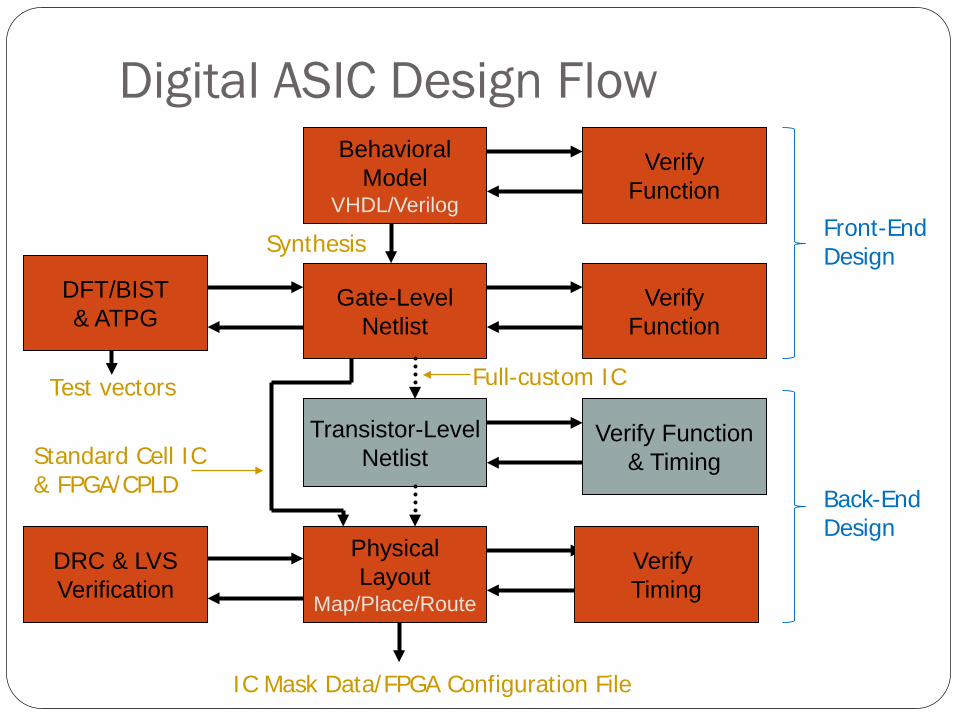
Digital ASIC Design FlowBehavioral
ModelVHDL/Verilog
Gate-LevelNetlist
Transistor-LevelNetlist
PhysicalLayout
Map/Place/Route
DFT/BIST& ATPG
VerifyFunction
VerifyFunction
Verify Function& Timing
Verify Timing
DRC & LVSVerification
IC Mask Data/FPGA Configuration File
Standard Cell IC & FPGA/CPLD
Synthesis
Test vectors Full-custom IC
Front-EndDesign
Back-EndDesign
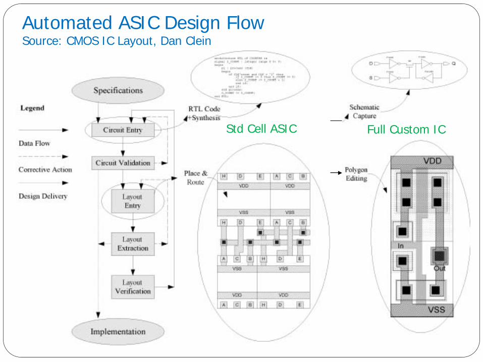
Automated ASIC Design FlowSource: CMOS IC Layout, Dan Clein
Std Cell ASIC Full Custom IC

Mentor Graphics Analog/Mixed-Signal “Pyxis” IC Design Platform
1
2
34
56
7

ASIC CAD tools available in ECE Modeling and Simulation
Questa ADMS = Questa+Modelsim+Eldo+ADiT (Mentor Graphics) Verilog-XL, NC_Verilog, Spectre (Cadence)
Design Synthesis (digital) Leonardo Spectrum (Mentor Graphics) Design Compiler (Synopsys), RTL Compiler (Cadence)
Design for Test and Automatic Test Pattern Generation Tessent DFT Advisor, Fastscan, SoCScan (Mentor Graphics)
Schematic Capture & Design Integration Pyxis Design Architect-IC (Mentor Graphics) Design Framework II (DFII) - Composer (Cadence)
Physical Layout Pyxis IC Station (Mentor Graphics) SOC Encounter, Virtuoso (Cadence)
Design Verification Calibre DRC, LVS, PEX (Mentor Graphics) Diva, Assura (Cadence)

IC Process Design Kits (PDKs) Foundry-specific data files and
models for CAD tools For a specific IC technology
Design components for both front-end & back-end design Schematic capture Simulation Physical layout Verification (DRC,LVS) DFT/test generation Cell libraries Device generators (RAM, etc.)
https://www.mentor.com/products/ic_nanometer_design/foundries/designkits
See list of foundries and PDKs available.
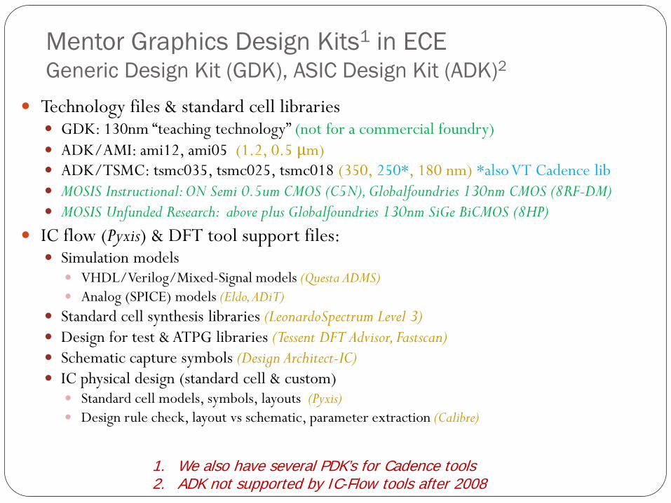
Mentor Graphics Design Kits1 in ECEGeneric Design Kit (GDK), ASIC Design Kit (ADK)2
Technology files & standard cell libraries GDK: 130nm “teaching technology” (not for a commercial foundry) ADK/AMI: ami12, ami05 (1.2, 0.5 μm) ADK/TSMC: tsmc035, tsmc025, tsmc018 (350, 250*, 180 nm) *also VT Cadence lib MOSIS Instructional: ON Semi 0.5um CMOS (C5N), Globalfoundries 130nm CMOS (8RF-DM) MOSIS Unfunded Research: above plus Globalfoundries 130nm SiGe BiCMOS (8HP)
IC flow (Pyxis) & DFT tool support files: Simulation models
VHDL/Verilog/Mixed-Signal models (Questa ADMS) Analog (SPICE) models (Eldo, ADiT)
Standard cell synthesis libraries (LeonardoSpectrum Level 3) Design for test & ATPG libraries (Tessent DFT Advisor, Fastscan) Schematic capture symbols (Design Architect-IC) IC physical design (standard cell & custom)
Standard cell models, symbols, layouts (Pyxis) Design rule check, layout vs schematic, parameter extraction (Calibre)
1. We also have several PDK’s for Cadence tools2. ADK not supported by IC-Flow tools after 2008
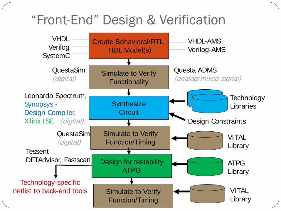
“Front-End” Design & VerificationCreate Behavioral/RTL
HDL Model(s)
Simulate to VerifyFunctionality
SynthesizeCircuit
Leonardo Spectrum,Synopsys -Design Compiler,Xilinx ISE (digital)
QuestaSim(digital)
VHDL-AMSVerilog-AMS
Questa ADMS(analog/mixed signal)
VHDLVerilog
SystemC
Technology Libraries
Technology-specific netlist to back-end tools
Simulate to VerifyFunction/Timing
VITALLibrary
Design Constraints
Design for testabilityATPG
Simulate to VerifyFunction/Timing
ATPGLibrary
VITALLibrary
TessentDFTAdvisor, Fastscan
QuestaSim(digital)

Questa ADMSAnalog, Digital, Mixed-Signal Simulation
Questa ADMS
WorkingLibrary
Design_1Design_2
VITAL
IEEE 1164
Resource Libraries
SimulationSetup
EZwave
InputStimuli
Design ModelsVHDL,Verilog, VHDL-AMS,
Verilog-AMS, SPICE
Eldo,Eldo RF QuestaSim
View ResultsADiTAnalog(SPICE) Digital
(VHDL,Verilog)
Mixed Signal(VHDL-AMS,
Verilog-AMS)
SPICEmodels
XilinxSIMPRIMS
ModuleGenerators

Questa ADMS Four simulation engines integrated for SoC designs
Questa – mixed signal simulation (VHDL-AMS, Verilog-AMS) QuestaSim (Modelsim) –VHDL/Verilog/SystemC digital simulation Eldo/Eldo RF – analog (SPICE) simulation ADiT – accelerated transistor-level (Fast-SPICE) simulation
Can mix engines/languages/standards in one simulation IEEE 1497 Standard Delay File Format (SDF) IEEE 1076.1 VHDL-AMS IEEE 1076 VHDL IEEE 1364 Verilog IEEE 1800 SystemVerilog IEEE 1666 SystemC Accellera standard Verilog-AMS Language SPICE Eldo, HSPICE, and Spectre dialects.

Questa ADMS : mixed-signal simulation
A/D converter
digitalVHDLanalogVHDL-AMS
digital nets
analog nets

Questa ADMS: mixed Verilog-SPICE
SPICEsubcircuit
Verilog top(test bench)

Automated Synthesis with LeonardoSpectrum/Synopsys Design Compiler
Leonardo Spectrum(Level 3)
Synopsys Design Compiler& Design Vision (GUI)
VHDL/Verilog Behavioral/RTL Models
FPGA
ASIC
TechnologySynthesis Libraries
Technology-SpecificNetlist
DesignConstraints
VHDL, Verilog, SDF,EDIF, XNF
Leonardo Spectrum:Level 1 – FPGALevel 2 – FPGA + TimingLevel 3 – ASIC + FPGA(we have Level 3 ASIC only)
Mentor ADK:AMI 0.5, 1.2TSMC 0.35, 0.25
Cadence ADKsTSMC 0.25Others
DW
Synopsys“DesignWare”Modules

Basic synthesis design flow
Predefined functions
Customfunctions

Leonardo – ASIC Synthesis Flow
Read &check HDL
Synthesizegeneric gates& modules
Map to technologycells & optimize
Write netlist,SDF, reports1
23
4
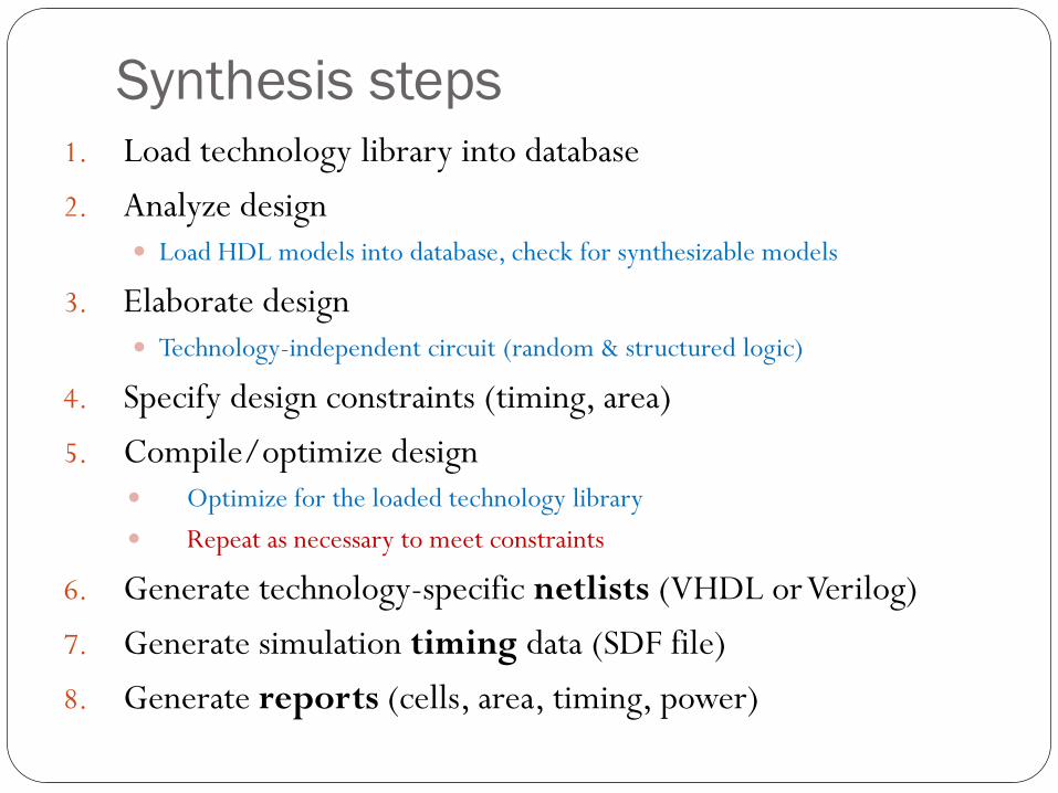
Synthesis steps1. Load technology library into database2. Analyze design
Load HDL models into database, check for synthesizable models
3. Elaborate design Technology-independent circuit (random & structured logic)
4. Specify design constraints (timing, area)5. Compile/optimize design
Optimize for the loaded technology library Repeat as necessary to meet constraints
6. Generate technology-specific netlists (VHDL or Verilog)7. Generate simulation timing data (SDF file)8. Generate reports (cells, area, timing, power)

Sample LeonardoSpectrum synthesis script load_library /linux_apps/ADK3.1/technology/leonardo/tsmc025_typ analyze "../src/mux.vhd" "../src/shiftreg.vhd" "../src/alu.vhd"
"../src/dcontrol.vhd" "../src/divider.vhd“ elaborate clock_cycle 2 CLOCK optimize -hierarchy preserve optimize_timing -through C/reg_State(2)/Q write divider_0.vhd write divider_0.v write_divider_0.sdf report_area div_area.rpt -cell_usage –hierarchy report_delay div_delay.rpt report_delay -longest_path -to Q* mod6_outdelay.rpt report_delay -longest_path -from [list I* L_Cbar] mod6_indelay.rpt
Synopsys Design Compiler script very similar
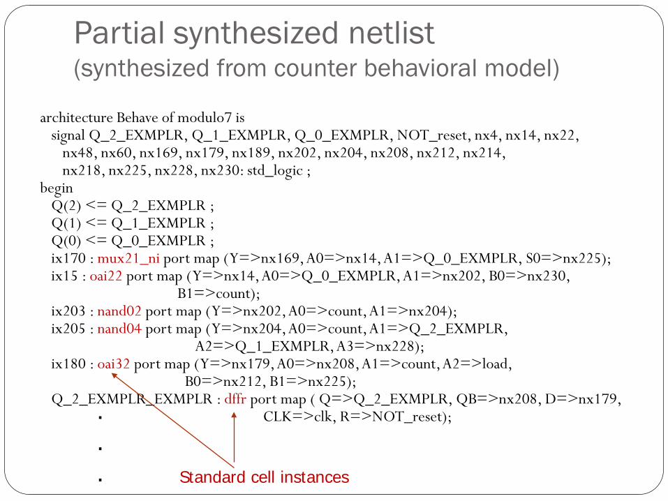
Partial synthesized netlist(synthesized from counter behavioral model)
architecture Behave of modulo7 issignal Q_2_EXMPLR, Q_1_EXMPLR, Q_0_EXMPLR, NOT_reset, nx4, nx14, nx22,
nx48, nx60, nx169, nx179, nx189, nx202, nx204, nx208, nx212, nx214, nx218, nx225, nx228, nx230: std_logic ;
beginQ(2) <= Q_2_EXMPLR ;Q(1) <= Q_1_EXMPLR ;Q(0) <= Q_0_EXMPLR ;ix170 : mux21_ni port map ( Y=>nx169, A0=>nx14, A1=>Q_0_EXMPLR, S0=>nx225);ix15 : oai22 port map ( Y=>nx14, A0=>Q_0_EXMPLR, A1=>nx202, B0=>nx230,
B1=>count);ix203 : nand02 port map ( Y=>nx202, A0=>count, A1=>nx204);ix205 : nand04 port map ( Y=>nx204, A0=>count, A1=>Q_2_EXMPLR,
A2=>Q_1_EXMPLR, A3=>nx228);ix180 : oai32 port map ( Y=>nx179, A0=>nx208, A1=>count, A2=>load,
B0=>nx212, B1=>nx225);Q_2_EXMPLR_EXMPLR : dffr port map ( Q=>Q_2_EXMPLR, QB=>nx208, D=>nx179,
CLK=>clk, R=>NOT_reset);
Standard cell instances
.
.
.

Post-synthesis simulation of netlist Verify that synthesized netlist matches behavioral/RTL model Create library of std cell simulation primitives:
>vlib adk>vcom $ADK/technology/adk.vhd>vcom $ADK/technology/adk_comp.vhd
Insert library/component declaration package into netlistlibrary adk;use adk.adk_components.all;
Simulate in Modelsim, using “do file” or test bench from the original behavioral simulation results should match
Simulate netlist with Leonardo-generated SDF file to study timing (delays, constraints, etc.)
VITAL models of ADK std cells

Design for test & test generation
Apply to synthesized (gate level) netlist as part of front-end design phase Test development more difficult after design netlist is frozen
Basic steps: Design for testability (DFT) – modify circuit structure to
improve testability; possibly insert test points, scan chains, etc. Insert built-in self-test (BIST) circuits Generate test patterns (ATPG) for the modified circuit Determine fault coverage (Fault Simulation)
Mentor Graphics Tessent Silicon Test tools support the above

Tessent – Test & Yield Analysis ToolsTessent FastScan
Tessent SoCScan& DFTAdvisor
Full/partial scan design,Test point insertion
ATPG/Fault simulation
Failure diagnosis
Statistical analysis of diagnosis data; find systematic yield limiters

Overall DFT & test design flow
Memory& LogicBIST Boundary
Scan
InternalScan Design
ATPG
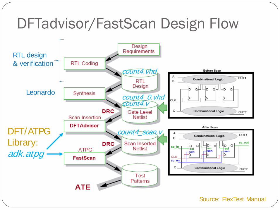
DFTadvisor/FastScan Design Flow
Source: FlexTest Manual
DFT/ATPGLibrary:adk.atpg
count4.vhd
count4_0.vhdcount4.v
count4_scan.v
Leonardo
RTL design& verification
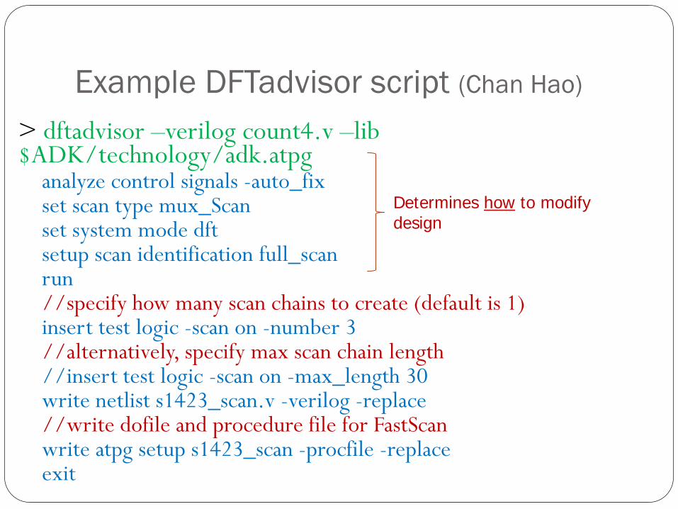
Example DFTadvisor script (Chan Hao)
> dftadvisor –verilog count4.v –lib $ADK/technology/adk.atpg
analyze control signals -auto_fixset scan type mux_Scanset system mode dftsetup scan identification full_scanrun//specify how many scan chains to create (default is 1)insert test logic -scan on -number 3//alternatively, specify max scan chain length//insert test logic -scan on -max_length 30 write netlist s1423_scan.v -verilog -replace//write dofile and procedure file for FastScanwrite atpg setup s1423_scan -procfile -replaceexit
Determines how to modifydesign
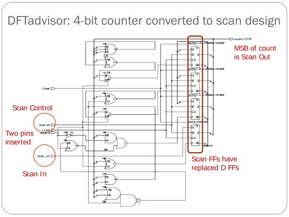
DFTadvisor: 4-bit counter converted to scan design
Scan Control
Scan In
Scan FFs have replaced D FFs
Two pins inserted
MSB of countis Scan Out

Invoke FastScan: fastscan –verilog count4.v –lib $ADK/technology/adk.atpg
Generate test pattern file: dofile count4_scan.dofile (define scan path & procedure)
set fault type Stuck (and/or other fault models)
add faults –all (or selected faults)
set system mode atpg create patterns –auto save patterns
Example FastScan script for ATPG (full-scan “counter” circuit)
created by DFTadvisor

Test pattern file (combinational logic ckt)
SETUP =declare input bus "PI" = "/A", "/B", "/C", "/D“ “/E”; declare output bus "PO" = "/Y";
end;
SCAN_TEST =
pattern = 0; force "PI" "00010" 0;measure "PO" "0" 1;
pattern = 1; force "PI" “01000" 0; measure "PO" “0" 1;
(3 lines per pattern)end;
I/O pin names(in order of vector bits)
Pattern #Input vectorExpected output for this pattern

APTG test patterns for scan-based test// send a pattern through the scan chainCHAIN_TEST =
pattern = 0;apply "grp1_load" 0 = (use grp1_load procedure)
chain "chain1" = "0011"; (pattern to scan in) end;apply "grp1_unload" 1 = (use grp1_unload procedure)
chain "chain1" = "1100"; (pattern scanned out)end;
end;// one of 14 patterns for the counter circuitpattern = 0; (pattern #)
apply "grp1_load" 0 = (load scan chain)chain "chain1" = "1000"; (scan-in pattern)
end;force "PI" "00110" 1; (PI pattern)measure "PO" "0010" 2; (expected POs)pulse "/clock" 3; (normal op. cycle)apply "grp1_unload" 4 = (read scan chain)
chain "chain1" = "0110"; (expected pattern)end;
Scan chains & load/unload proceduresdefined earlierin the file.
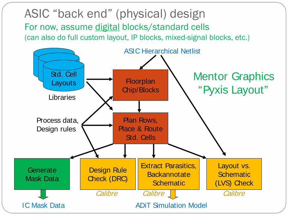
ASIC “back end” (physical) designFor now, assume digital blocks/standard cells (can also do full custom layout, IP blocks, mixed-signal blocks, etc.)
FloorplanChip/Blocks
Plan Rows,Place & Route
Std. Cells
ASIC Hierarchical Netlist
IC Mask Data
Design RuleCheck (DRC)
Std. CellLayouts
Mentor Graphics“Pyxis Layout”
ADiT Simulation Model
Extract Parasitics,Backannotate
Schematic
GenerateMask Data
Layout vs.Schematic
(LVS) Check
Process data,Design rules
Libraries
Calibre Calibre Calibre
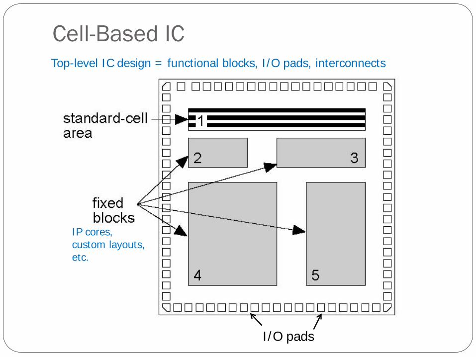
Cell-Based IC
I/O pads
Top-level IC design = functional blocks, I/O pads, interconnects
IP cores,custom layouts,etc.
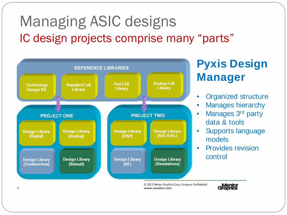
Managing ASIC designsIC design projects comprise many “parts”
Pyxis Design Manager
• Organized structure• Manages hierarchy• Manages 3rd party
data & tools• Supports language
models• Provides revision
control

Project: all elements of a design projectLibrary: within a project, contains IC data created by the designerExternal Library: reference library of IC design data (static)Logic Library: reference library of “logic” (process independent) dataTechnology Library: symbols, parameterized devices, rule decks, simulationsCategory: container within a library for one type of IC design dataComponent Set: virtual grouping of cellsCell: one element of a hierarchical IC design (schematic, layout, other views)
PyxisProjectNavigator
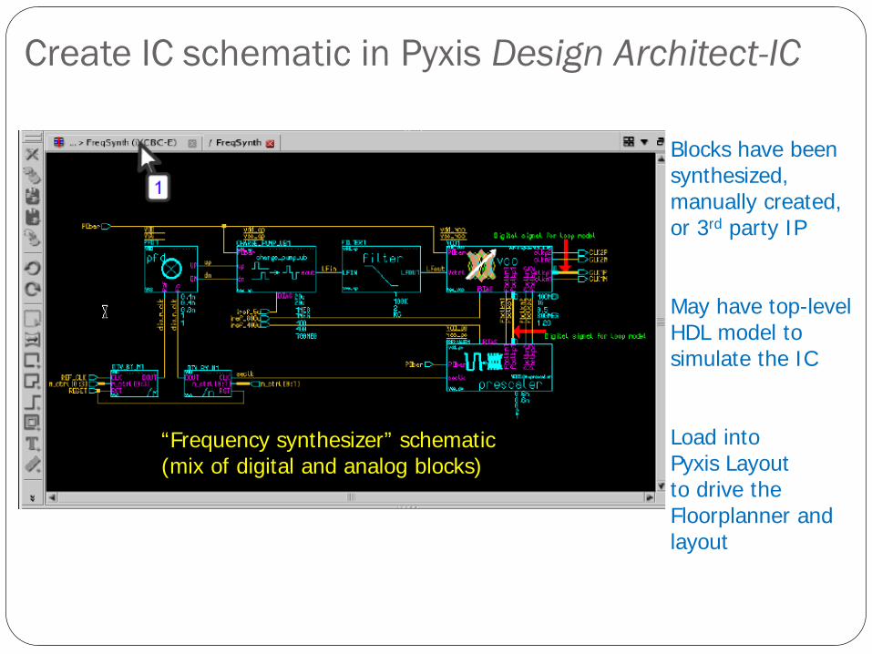
Create IC schematic in Pyxis Design Architect-IC
Blocks have beensynthesized, manually created,or 3rd party IP
May have top-levelHDL model tosimulate the IC
Load intoPyxis Layout to drive the Floorplanner and layout
“Frequency synthesizer” schematic(mix of digital and analog blocks)

Pyxis Layout Floorplanner auto-places schematic blocks
• Block sizes estimated from corresponding netlists/layouts• Resize, reshape, rearrange blocks as desired
Overflowsshow blockconnections

Floorplan after modifying blocks and placementIncludes IC cell boundary box
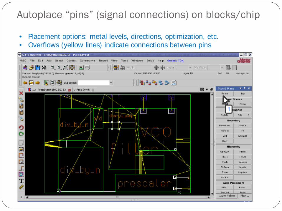
Autoplace “pins” (signal connections) on blocks/chip
• Placement options: metal levels, directions, optimization, etc.• Overflows (yellow lines) indicate connections between pins
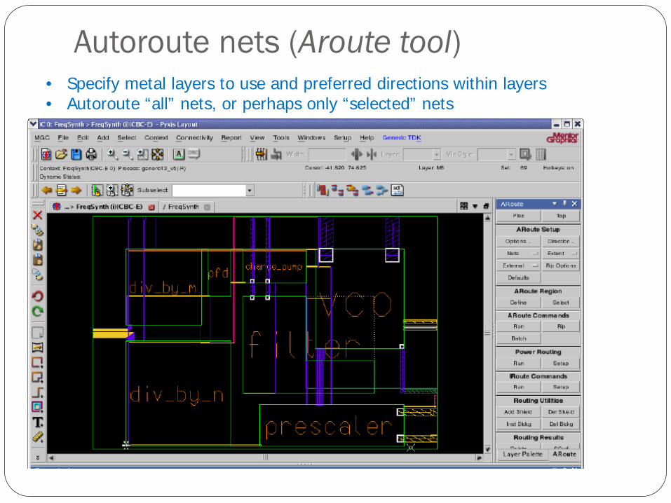
Autoroute nets (Aroute tool)• Specify metal layers to use and preferred directions within layers• Autoroute “all” nets, or perhaps only “selected” nets

Design rule check (DRC) with Calibre (fix any errors)
Spacing errorbetweenmetal 4lines
Calibre Results Verification (RVE) Window identifies errors
Highlight the error(metal 4, rule 5.3)

Automated block layout(assume digital block – using standard cells)
Pyxis Assemble basic steps1. Select the block in the IC
floor plan2. Flatten the digital block
hierarchy3. Plan cell rows to fit the block4. Place standard cells and
feedthrough cells5. Create power rings6. Autoroute connections7. Perform DRC and LVS –
correcting errors as needed
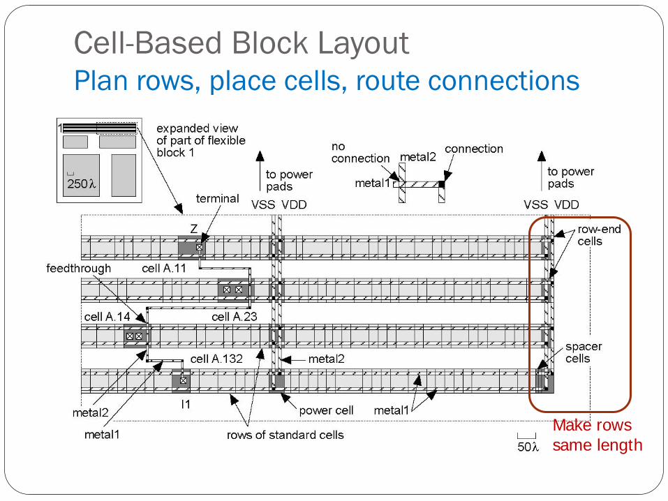
Cell-Based Block LayoutPlan rows, place cells, route connections
Make rows same length
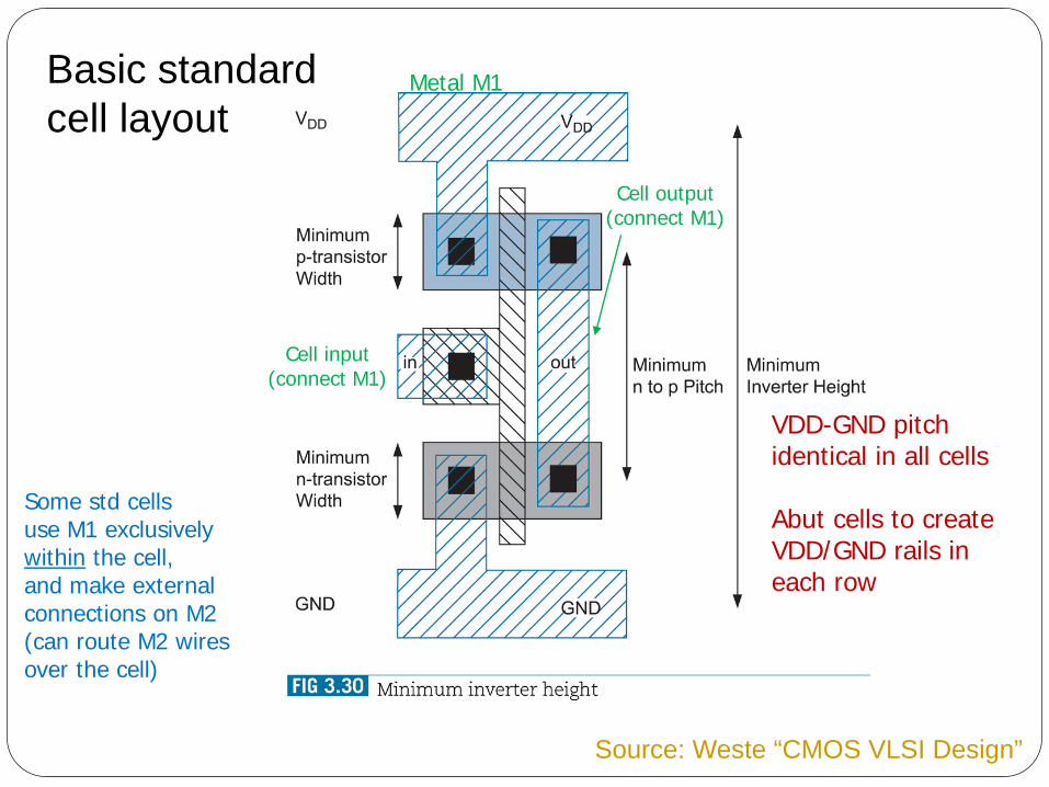
Source: Weste “CMOS VLSI Design”
Basic standardcell layout
VDD-GND pitchidentical in all cells
Abut cells to createVDD/GND rails ineach row
Cell input(connect M1)
Cell output(connect M1)
Metal M1
Some std cellsuse M1 exclusivelywithin the cell,and make external connections on M2(can route M2 wiresover the cell)

1. Select “StdCellAutoplace”
3. Select“Feed”
4. Select “Slide row left” and “Fill row” with feedthrucells
Placing standard cells and feedthrough cellsAfter: select block, flatten hierarchy, and plan cell rows/edge gaps (for power)
6 cellrows
Divide-by-n block

Add power routing and power rings• VDD/GND wires of rows connect to rings in “edge gap” around the block• Using Plan & Route palette, desired metal levels selected
Powerrings

Autoplace pins on the block
1. Select the block
2. Click “Plan”
3. Click “Autoplace Pins”
4. Select metal levels for pins onthe 4 sides(match routing directions)

Autoroute (ARoute) to connect cells/pins1. Select metal levels and directions for wires
2. Undo/redo routingas desired
3. Autoroute“all” or onlyselected nets

Route any unfinished signals (IRoute tool)
• Autoroute can leave overflows• Select an overflow & guide the router
Select IRoute (Interactive Routing)
Click to select unrouted port
Hotkey “p” =>“push” M1-M3 viasout of the way(“p,p” => 2 directions)
LBM click to define a route pointbelow congested area
Go!
Selectroutingoptions
Mx
My
Mx-My “Via”

Completed block layoutVerify layout periodically via DRC/LVS
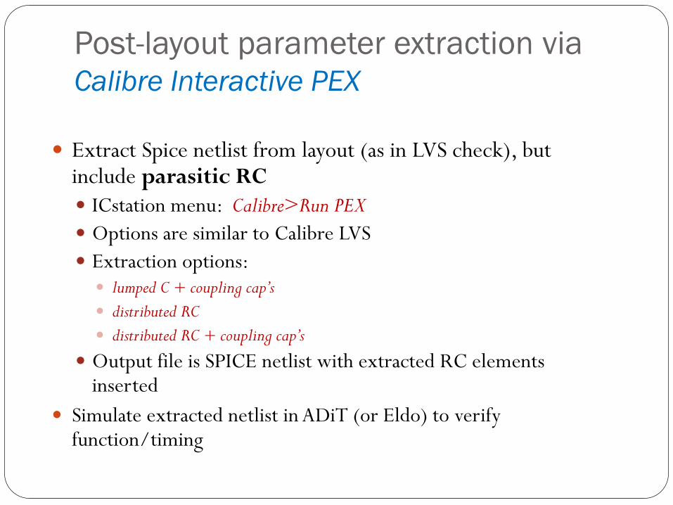
Post-layout parameter extraction viaCalibre Interactive PEX
Extract Spice netlist from layout (as in LVS check), but include parasitic RC ICstation menu: Calibre>Run PEX Options are similar to Calibre LVS Extraction options: lumped C + coupling cap’s distributed RC distributed RC + coupling cap’s
Output file is SPICE netlist with extracted RC elements inserted
Simulate extracted netlist in ADiT (or Eldo) to verify function/timing
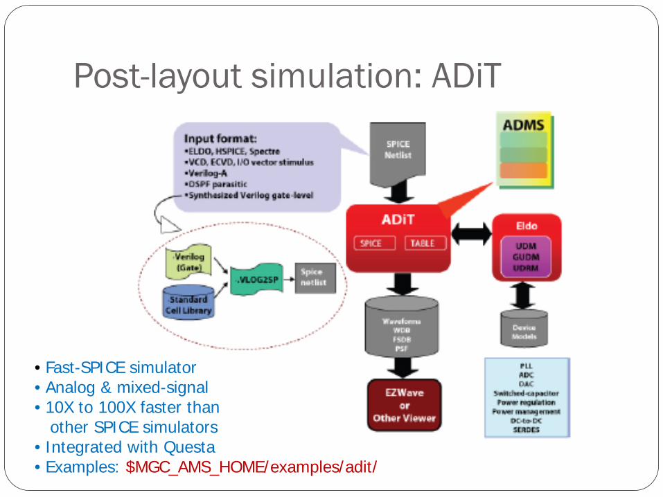
Post-layout simulation: ADiT
• Fast-SPICE simulator• Analog & mixed-signal• 10X to 100X faster than
other SPICE simulators• Integrated with Questa• Examples: $MGC_AMS_HOME/examples/adit/

Digital simulation in ADiT ADiT supports digital vectors (unlike SPICE simulators) SETBUS - define a “bus” containing digital signals SIGBUS - Stimulate a bus with test vectors PLOTBUS – capture and plot digital bus values CHECKBUS – capture & compare bus value to expected value
ADiT supports test vector files, similar to a “pattern file” for an IC tester Pattern = vector to apply to inputs + expected output pattern
Measure and Extract commands support verification of timing parameters by extracting waveform characteristics (delays between signal edges, etc.)

Further information ELEC 5250/6250 (CAD of Digital ICs) web pagehttp://www.eng.auburn.edu/~nelsovp/courses/elec5250_6250/ Lecture slides Links to CAD tool resources and papers Links to VHDL resources
Mentor Graphics tools available only on COE Linux server Secure shell and X-Server tools required to log in and run tools
Ex. MobaXterm - combines both tools Configure .bashrc file in your home directory with
paths/environment variables for Mentor Graphics tools Sample .bashrc file posted on the above web page
Use Mentor Graphics mgcdocs command to access bookshelves of documentation (pdf/html files)
See usage of mgcdocs on the above web page