compact - hamamatsu photonics · the result and solution are our sipm ... the ultimate detector....
TRANSCRIPT

MPPCs® – Multi-Pixel Photon Countersfor High Energy Physics Experiments
Cover Story PAGe 2
for Low-Light
CompactInstrumentation
Detection
W-VIEW GEMINI – simultaneous dual wavelength imaging
SySteMS ProDUCtS PAGe 24
Fingertip size, ultra-compact Micro-Spectrometer
oPto-SeMICoNDUCtor ProDUCtS PAGe 11
The world's smallest, thinnest and lightest Micro PMT Module
eLeCtroN tUBe ProDUCtS PAGe 17
2014
01

News 2014 Vol. 12
Cover Story
MPPCs® – Multi-Pixel Photon Counters for High Energy Physics Experiments
Imagine – The Ultimate Detector
once again, the HeP (High energy Physics) community triggered a development that influenced, in this case, the whole Photonics world and eventually daily life too.
the goal of the community was to be able to count photons over a large area, under strong magnetic fields. the detector should work at room temperature and yes, it would be nice if it could be very fast too. the HeP community also made clear that to succeed we needed to offer the new technology at very challenging prices.
With the help of the HeP community, Hamamatsu Photonics accepted this challenge and together we started with the well-known Geiger-Mode effect in an avalanche diode. that meant we had to go from an active surface of some tens of microns, cooled down to -20/40 deg. C., to surfaces of square meters and of course uncooled.
We are proud to say that we succeeded in this challenge!
the result and solution are our SiPM (Silicon Photo Multipliers) called MPPC® (Multi Pixel Photon Counters). Instead of having just one active area, we covered a large surface with thousands of avalanche
pixels, each of them with its own quenching resistor. Pair this idea together with Hamamatsu's design and outstanding solid state physics knowledge and state-of-the-art in-house processing with MoeMS capabilities, and you have – The Ultimate Detector. the MPPCs are the result of years of work, research and hundreds of prototypes.
MPPCs enable photon counting at room temperature, with relatively high dynamic range, high speed, at low voltages and in the size of a standard photodiode, all for a reasonable cost. So the HeP community reached its goal too and they will be able to use the MPPCs for building various detectors like Calorimeters, trackers, triggers and cameras for Astrophysics etc. the first application to use this technology outside the HeP community has been in nuclear medicine and the first Pet Scanners using our MPPC will soon be on the market. But all other fields in Photonics recognized the potential of our new technology and are catching up fast by adopting the MPPC in their new developments, like LIDAr and analytical applications. And since it is basically a "normal" photodiode, we can customize it in any active area shape desired. We can form 1D or 2D monolithic arrays or in discrete assemblies in various packages.
Imagine what you could do with the ultimate detector!
the cover picture shows the first light map of the gamma-ray sky taken by Fermi Gamma-ray Space telescope.
the Fermi Gamma-ray Space telescope was equipped with Hamamatsu Photonics photomultiplier tubes and silicon strip sensors.
this is just one example where Hamamatsu Photonics worked closely with the scientists to provide technology solutions for a demanding High energy Physics experiment.
News 2014 Vol. 1 3
Content
Academ
ic rese
arch
ND Inspe
ction
Indust
ry
Secu
rity
optical
Comms
Semico
nd. P
rod.
Analyt
ical
Measur
emen
t
Drug Disc
overy
Life S
cienc
e
Medica
l
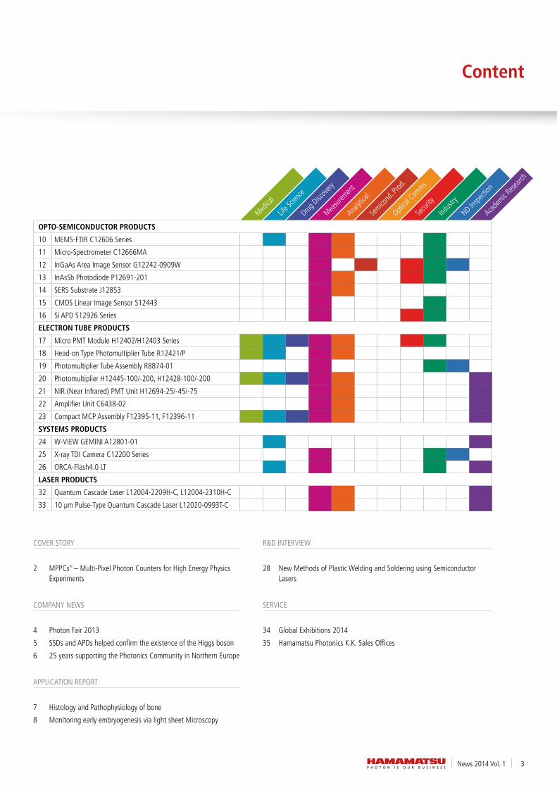
OPTO-SEMICONDUCTOR PRODUCTS
10 MeMS-FtIr C12606 Series
11 Micro-Spectrometer C12666MA
12 InGaAs Area Image Sensor G12242-0909W
13 InAsSb Photodiode P12691-201
14 SerS Substrate J12853
15 CMoS Linear Image Sensor S12443
16 Si APD S12926 Series
ELECTRON TUBE PRODUCTS
17 Micro PMt Module H12402/H12403 Series
18 Head-on type Photomultiplier tube r12421/P
19 Photomultiplier tube Assembly r8874-01
20 Photomultiplier H12445-100/-200, H12428-100/-200
21 NIr (Near Infrared) PMt Unit H12694-25/-45/-75
22 Amplifier Unit C6438-02
23 Compact MCP Assembly F12395-11, F12396-11
SYSTEMS PRODUCTS
24 W-vIeW GeMINI A12801-01
25 X-ray tDI Camera C12200 Series
26 orCA-Flash4.0 Lt
LASER PRODUCTS
32 Quantum Cascade Laser L12004-2209H-C, L12004-2310H-C
33 10 µm Pulse-type Quantum Cascade Laser L12020-0993t-C
Cover Story
2 MPPCs® – Multi-Pixel Photon Counters for High energy Physics experiments
CoMPANy NeWS
4 Photon Fair 2013
5 SSDs and APDs helped confirm the existence of the Higgs boson
6 25 years supporting the Photonics Community in Northern europe
APPLICAtIoN rePort
7 Histology and Pathophysiology of bone
8 Monitoring early embryogenesis via light sheet Microscopy
r&D INtervIeW
28 New Methods of Plastic Welding and Soldering using Semiconductor Lasers
ServICe
34 Global exhibitions 2014
35 Hamamatsu Photonics K.K. Sales offices

News 2014 Vol. 14
Now availableVirtual PHOTON FAIR released
www.photonfair.jp/en/
Company News
PHOTON FAIR 2013
Hamamatsu Photonics K.K. exhibition PHotoN FAIr 2013 was held from the 7th to 9th November 2013, in celebration of Hamamatsu Photonics' 60th anniversary. through the main theme "Leading with Light," we presented our latest optical technology and products and suggested various ways in which optical technology will contribute greatly to advanced manufacturing.
the event ended on a high note. We also held lecture presentations by invited external speakers, our Ceo and the executive managing director of each division.
In addition many visitors participated in the approximately 40 technical seminars held by our employees.
We had released virtual PHotoN FAIr which contains the essences of PHotoN FAIr 2013.
the contents include cutting-edge global projects and showcase the very latest Hamamatsu products and technologies. Please visit the website for further information.
virtual Photon Fair includes video interviews of the persons in charge of product development, and a live report direct from the exhibition.

News 2014 Vol. 1 5
Company News
Silicon strip detectors installed in the CMS experimental apparatus (courtesy of CERN)
The CMS Award received from CERN in 2003 and 2005
SSDs and APDs helped confirm the existence of the Higgs boson
the LHC (Large Hadron Collider) project of CerN (the european organization for Nuclear research) stretches 27 km. For its sensors, it uses SSDs (silicon strip detectors), APDs (avalanche photodiodes), and PMts (photomultiplier tubes).
SSDs used in the ATLAS and CMS experimental apparatus to detect particle tracksApproximately 14,000 SSDs are used for the AtLAS experiment, 22,000 for the CMS experiment and an SSD is a diode array in a strip shape. It detects the positions particles pass through with a resolution of several tens of µm.
APDs used as calorimeters in the CMS experimentthe APDs have a photosensitive area of 5 mm by 5 mm. they are used in combination with scintillators. to achieve optimal per formance under harsh conditions in a strong magnetic field with radiation, opto semi conductors were used, which are strong in strong magnetic fields.
What is the Higgs boson?the Higgs boson is a particle that gives all kinds of matter mass. It is known as the "God particle," but had not been discovered until now. CerN (the europ ean organization for Nuclear research) was trying to confirm the existence of the Higgs boson by continued experiments at their Large Hadron Collider (LHC), the world's largest particle accelerator, a 27 km circuit in suburban Geneva, Switzerland. In 2013, its existence was confirmed, and emeritus professors Francois englert and Peter Higgs, who foretold its existence half a century earlier, were awarded the 2013 Nobel Prize in Physics.
When protons collide near the speed of light, the energy causes the creation of new particles. Hamamatsu Photonics' sensors are used to investigate the nature of the particles by detecting the direction (track) they fly and their energy.
In the equipment for the AtLAS and CMS experiments, SSDs have been used to detect particle tracks (supplied since 1999). PMts are used to detect minute light for calorimeters to detect particle energy in AtLAS and CMS, and APDs are used in CMS.

Moscow
News 2014 Vol. 16
Company News
25 years supporting the Photonics Community in Northern Europe
the Northern european branch of Hamamatsu was established in Stockholm, Sweden, at the end of the eighties, with the primary goal to develop the local support of existing and potential business opportunities in Scandinavia and Finland.
Being a small scale operation with a handful of team members in the beginning, the business and the organization developed successfully over the years and today Hamamatsu Photonics Norden AB (HPN) is a well-recognized and active partner in the photonics community in the Nordic countries, supporting development of scientific and industrial projects within a wide range of technologies and application fields.
the changes in europe during the nineties opened up exciting possibilities to develop business in eastern europe and as a consequence a representation office was established in Moscow at the beginning of the new millennium, offering local service and support to all our customers and partners in russia and CIS (Commonwealth of Independent States).
Stockholm
Max Skoglund, Managing Director, would like to thank all customers during these 25 years for a fruitful and successful cooperation. HPN will continue aiming to be the natural choice for customers interested in photonics, striving to have a flexible organization with a qualified group of staff, co-operating with present and potential customers to develop profitable business solutions for our products and services.

News 2014 Vol. 1 7
Application Report
Histology and Pathophysiology of bone
Pathophysiology of Bone Resorption Laboratory, INSERM UMR957,Nantes University, FranceIn 2011, our research laboratory acquired a digital slide scanner, the Hamamatsu NanoZoomer 2.0-rS. It converts up to 6 glass slides into digital slides by scanning them automatically and quickly at high resolutions (up to x40). the purchase was made possible thanks to INSerM (Plan Cancer 2009-2013).
Bone cancer researchWe are interested in the molecular and cellular mechanisms involved in the pathogenesis of bone tumors. our works cover the basic research, the preclinical and clinical aspects in this field.
Example A: First, this slide scanner allows us to more easily archive digital slides without worrying about sample deterioration. this is especially important in animal ex perimentations where hundreds of slides are typically analyzed at the same time.
Secondly, digital slides are easy to send to our collaborators in France or other countries for expertise or even diagnosis. Primary bone tumors such as osteo-sarcoma are rare diseases and the expert pathologists in the field are now questioned by email.
Lastly, image view, annotation and analysis can be performed “at home” on any computer, especially when using a file storage online. researchers and students can now count, for example, bone cells (osteoblasts, osteoclasts etc) from anywhere, anytime they want.
Education, training and popular scienceUsing the NanoZoomer and its digital slides renders easier to explain bone histology, immunohistochemistry or in situ hybridization to students in an amphitheater, technicians at the bench or even to the public.
Low resolution viewExample B: In comparison to standard microscopy, the low resolution images obtained with the NanoZoomer are clearer and brighter, which is especially interesting to visualize a whole organ or tissue such as bone or primary tumor.
Automation of analysisAs an option (not used in the lab), combining the NanoZoomer to NDP.Analyze provides the ability to log on and analyze digital slides from anywhere. Sophisticated APPs (Application Protocol Packages) can be operated locally or via Cloud computing.
Authors: Pr D. Heymann and Dr F. Blanchard
Example A
Bone cancer research
Example B
Microscope (1.6x) NanoZoomer (1.6x)
Osteoclasts (40x)
Overview (0.4x) Cartillage (0.9x)

News 2014 Vol. 18
Monitoring early embryogenesis via light sheet Microscopy
Single-plane illumination microscopy (SPIM) is a fluorescence imaging technique that combines rapid wide-field detection with optical sectioning. By reducing phototoxicity induced by bleaching, SPIM is capable of providing a long-term, three-dimensional and time-resolved in vivo imaging of specimen.
"We have built and automated a SPIM setup specifically designed for imaging the early stages of embryogenesis of the small nematode Caenorhabditis elegans" explains Philipp Struntz, graduate student in the group of Prof. Matthias Weiss (Dept. of experimental Physics I, University of Bayreuth). the setup consists of the widened beam of a 491.5 nm DPSS-laser, which is focused in one dimension by a cylindrical lens onto the back-focal plane of a water-dipping objective to form an elliptically deformed Gaussian beam that serves as light sheet (minimum waist of 2.8 mm FWHM). Fluorescence from the sample is collected perpendicular to the illumination light sheet by a second water-dipping objective. Fluorescence light is filtered and focused onto the sensor of an orCA-Flash 4.0 sCMoS-camera (Hamamatsu Photonics). the lateral and axial extension of the setup’s point-spread function was determined with FluoSpheres (diameter 20 nm) to be 460 nm and 1.4 mm in the light sheet waist.
Laserbeam
cylindricallense
sample
Orca-Flash 4.0z
y
x
y
mirror
objectives
mirror
filter andtube lense
As can be seen from figure 1, objectives are arranged in an angle of 45° degree with respect to the optical table. the sample is moved with respect to the light sheet by two motorized stages in xy-direction. A nanopositioner allows for moving the sample through the light sheet with a precision of a few nm, hence enabling the acquisition of three-dimensional image stacks of the sample.
the setup is controlled via a custom-made LabvIeW program that also has an interface to the HoKAWo imaging software (Hamamatsu Photonics) that controls the camera.
Post-processing of raw images, i.e. aligning individual sections to obtain three-dimensional data, is done with a custom-made Matlab code. With this approach, nuclei can be tracked in the developing embryo and even division axes during mitotic events can be assessed.
Figure 1: SPIM-Setup: Sketch of the beam path of the custom-made SPIM. All parts left from the dashed line are shown from the top whereas all parts on the right are shown from the side.
Application Report

News 2014 Vol. 1 9
Application Report
Philipp Struntz explains the experiment conditions: We repetitively acquired 51 optical sections (separated by a distance of 2 µm) of a C.elegans embryo with an exposure time of 50 ms per layer. Stack acquisition was repeated every 60 s to cover early developmental processes. representative individual sections of this imaging are shown in figure 2a, the maximum projection obtained from the three-dimensional data is depicted in figure 2b. Since cell lineages in C. elegans are invariant, not only trajectories but also the type of individual cells could be identified in three dimensions over time. An example is shown in figure 2c.
Based on our data, we observed in all cases a planar cell arrangement in 4-cell embryos, and cell movements and division axes were strikingly similar between embryos, states Philipp Struntz. It is tempting to conclude on this basis that mechanical cues support the cell arrangement in early C. elegans embryogenesis*. the obtained time lapse images allowed us to quantitatively monitor individual cell positions and division axes within the developing embryo. these data build a valuable starting point for a deeper understanding of the spatiotemporal dynamics of developing tissues.
-20
020
40
-30-20-1001020
-30
-20
-10
0
10
20
x [µm]y [µm]
z [µm]
EMSP2
P3CE
MS
ABpl
ABpr
ABp
ABal
ABar
ABa
Figure 2: a) Different layers of a C. elegans embryo (long axis 50 μm) in the 8-cell stage. b) Maximum projection of all 51 sections of the embryo in (a), showing all 8 nuclei
positions with a high contrast. c) Example of three-dimensional cell trajectories. Cells are color-coded and named.
Cell divisions are visible as branching points of trajectories.
a) b) c)
Prof. Matthias Weiss concentrates in his research on challenging problems at the interface of physics and biology. His group focuses on a quantitative understanding of intracellular transport processes, on elucidating interactions of proteins and membranes, and on the dynamics and self-organization of eukaryotic cells from the organelle to the organismal level.
* Fickentscher, Struntz and Weiss, Mechanical cues in the early embryogenesis of Caenorhabditis elegans, to appear in Biophys. J. 105(8), (2013).
For further information see the website of the Dept.
of Experimental Physics I, University of Bayreuth,
http://www.ep1.uni-bayreuth.de/weiss/en/index.html

oPto-SeMICoNDUCtor ProDUCtS
10 News 2014 Vol. 1
NEWMEMS-FTIR C12606 Series
Academ
ic res.
ND Inspe
ction
Indust
ry
Secu
rity
optical
Comms
Semico
n Prod
.
Analyt
ical
Measur
emen
t
Drug Disc
overy
Life S
cienc
e
Medica
l
Compact NIR spectrometer with a built-in fingertip size MEMS-FTIR engine
MeMS-FtIr (Fourier transform Infrared) spectrometer is a compact and low-cost Fourier transform infrared spectrometer, where a Michelson Interferometer and infrared detector are packaged in a small housing. Connecting it to a PC via a USB cable allows spectrum measurement and absorbance measurement.
C12606 series
SEM image of MEMS interferometer
Specifications
Parameter Symbol C12606-01 C12606-02 UnitSpectral response range λ 1.15 to 1.65 1.15 to 2.05 µm
Spectral resolution (FWHM) *1 Δλ 8 (λ =1.65 µm) 12 (λ =2.05 µm) nm
SNr *225 deg. C.
-30 29
dB40 deg. C. 29 25
Scan rate *3 - 5 ms
Dimensions (W x D x H) - 100 x 75 x 27 mm
*1 About 29 cm-1 in wavenumber*2 on a condition of about 600 µW white light input at a fiber (φ200 µm, NA = 0.2), 1 s integration time*3 the minimum time to acquire an optical spectrum, cutoff frequency: 200 Hz
Optical fiber
Beam splitter
Fixed mirror
Moving mirror
Electro static actuator
Optical fiber
Glucose solution measurement
Glucose density can be estimated with high degree of accuracy by using MeMS-FtIr.
Standardization absorbance spectrum
Glucose solution measurement
Glucose density can be estimated with high degree of accuracy by using MEMS-FTIR.*
-4
-3
-2
-1
0
1
2
3
1300 1400 1500 1600 1700
Stan
dard
ized
abso
rban
ce
Wavelength (nm)
0 %Glucose density
0.1 %0.25 % 0.5 %1 % 2.5 %5 % 10 %
(1 mm quartz cell, PLS Regression analysis)R2 = 0.994SEP = 0.273RPD = 12.68
Standardization absorbance spectrum Result of glucose estimation
0 2 4 6 8 10 12Actual glucose (%)
Pred
icted
glu
cose
(%)
D* (c
m ·
Hz1/
2 /W)
-2
0
2
4
6
8
10
12
Result of glucose density estimation
Ultra compact FTIR engine

oPto-SeMICoNDUCtor ProDUCtS
11News 2014 Vol. 1
Hollow
Entrance slitCMOS linear image sensor with a slit
Reflective concave brazed grating
Grating chip
Incidentlight
Optical component layout (C10988MA)
KACCC0757EB
Structure
Micro-Spectrometer C12666MA
Fingertip size, ultra-compact spectrometer head integrating MEMS and image sensor technologies
A micro-spectrometer is an ultra-compact spectrometer head developed utilizing MeMS and image sensor technologies. the adoption of a newly designed optical system has achieved a remarkably small size, less than half the volume of the previous mini-spectrometer MS series (C10988MA-01). Its package is hermetically sealed for high reliability versus humidity. the spectral response range is from 340 to 780 nm and so is used to measure light in the visible region. Micro-spectrometers are ideal for assembly into portable equipment requiring color control such as handheld color monitors and printers.
Features Fingertip size: 20.1 × 12.5 × 10.1 mm Weight: 5 g Hermetic package: high reliability against humidity Installation into mobile measurement equipment Designed for use in combination with portable devices such as smartphones and tablets
Applications Color monitoring for printers and printing machines testers for lights and LeDs Color adjustment of various large size displays Water quality control monitors and other environment measuring instruments
NEW
Specifications
Parameter Value UnitSpectral response range 340 to 780 nm
Spectral resolution (FWHM) 15 max. nm
Spectral stray light *1 -25 dB
Slit (H x v) 50 x 750 µm
NA 0.22 -
Number of pixels 256 pixels
Pixel size (H x v) 12.5 x 1,000 µm
Dimensions (W x D x H) 20.1 x 12.5 x 10.1 mm
*1 Spectral stray light = 10 x log (tl/th) th: count measured when light at a certain wavelength is input tl: count measured at a wavelength 40 nm longer or shorter than the input light wavelength
C12666MA
ND Inspe
ction
Indust
ry
Secu
rity
optical
Comms
Semico
n Prod
.
Analyt
ical
Measur
emen
t
Drug Disc
overy
Life S
cienc
e
Medica
l
Academ
ic res.
Application examples
Color adjustment of color printers
Simple color measurements using smartphones
Handheld type color monitor equipment

oPto-SeMICoNDUCtor ProDUCtS
12 News 2014 Vol. 1
InGaAs Area Image Sensor G12242-0909W
2-D InGaAs image sensor for easily capturing a near infrared image
the two-dimensional InGaAs image sensor G12242-0909W is a sensor for easily capturing a near infrared image. An InGaAs photodiode chip is connected with roIC, and then each channel is read out from a shift-register. the roIC incorporates a timing generator, so video output can be obtained by simple digital input. the temperature of the InGaAs photodiodes in the package can be controlled constantly with a built-in te-cooler and a thermistor.
Features Spectral response range: 0.95 to 1.7 µm 640 x 512 pixels two-stage te-cooled type Preparing a multichannel detector head (C12376)
Applications Semiconductor wafer defect analysis Person recognition in low visibility environment Near infrared imaging
Near-infrared imaging of a color-painted wooden airplane toy makes visible the cracks, traces of resin, and characters underneath the paint layer, etc.
NEW
Academ
ic res.
ND Inspe
ction
Indust
ry
Secu
rity
optical
Comms
Semico
n Prod
.
Analyt
ical
Measur
emen
t
Drug Disc
overy
Life S
cienc
e
Medica
l
Specifications
Parameter Symbol Value UnitNumber of pixels - 640 x 512 pixels
Pixel pitch - 20 µm
Peak sensitivity wavelength λp 1.55 µm
Frame rate - 30 frames/s
Conversion efficiency Ce 2 µv/e-
Saturation charge Qsat 500 ke-
Saturation output voltage vsat 1 v
Photoresponse nonuniformity PrNU ±10 %
Dark output vD 6.25 v/s
G12242-0909W

oPto-SeMICoNDUCtor ProDUCtS
13News 2014 Vol. 1
P12691-201
InAsSb Photodiode P12691-201
InAsSb photodiode with high-speed response and high sensitivity in the 8 μm spectral band
the P12691-201 is an infrared detector that provides high sensitivity in the 8 µm spectral band by integrating a lens using our unique crystal growth technology and back-illuminated structure. the InAsSb photodiode has a PN junction that ensures high-speed response and high reliability. typical applications include gas analysis such as No, No2, and N2o. the P12691-201 is easy to use as it uses a compact te-cooled package (to-8) not requiring liquid nitrogen.
Features High speed response High sensitivity High reliability Compact, thermoelectrically cooled to-8 package roHS compliant Can be assembled in a module with QCL
Applications
Gas analysis radiation thermometers thermal imaging remote sensing FtIr Spectrophotometers
NEW
KIRDB0592EA
3 64 5 8 97 1010 7
10 9
10 8
10 10
Wavelength (µm)
D* (c
m ·
Hz1/
2 /W)
Spectral response (P12691-201)
(Typ. Td=-30 °C)
Spectral response (typ. td = -30 deg. C.)
Specifications
Parameter Condition Min. Typ. Max. UnitPhotosensitive area - φ 1.0 mm
Peak sensitivity wavelength - - 6.7 - µm
Cutoff wavelength - 8.2 8.3 - µm
Photosensitivity λ = λp 0.8 1.2 - A/W
Shunt resistance vr = 10 mv 13 40 - Ω
Detectivity (λp, 600, 1) 4.0 x 10⁹ 6.0 x 10⁹ - cm • Hz1/2/W
Noise equivalent power (NeP) λ = λp - 1.5 x 10⁻¹¹ 2.3 x 10⁻¹¹ W/Hz1/2
rise timevr = 0 v, rL = 50 Ω
0 to 63 %- - 10 ns
ND Inspe
ction
Indust
ry
Secu
rity
optical
Comms
Semico
n Prod
.
Analyt
ical
Measur
emen
t
Drug Disc
overy
Life S
cienc
e
Medica
l
Academ
ic res.

oPto-SeMICoNDUCtor ProDUCtS
14 News 2014 Vol. 1
SERS Substrate J12853
SERS substrate suitable for high-sensitivity Raman spectroscopic analysis
the SerS* substrate is a disposable substrate using nanoimprint technology, and can be used to enhance raman scattering light for molecular measurement. It facilitates high-sensitivity raman spectroscopic analysis.
Features Uniform activated surface structure
the activated surface structure that enhances raman scattering light (active area) is made of gold. Nanoimprint technology is used to form a fine pattern to produce a uniform structure.
Structure for protecting the active area to effectively produce the performance of the SerS substrate, adsorption of contamination of the activated structure (active area) on the SerS chip must be prevented.
Easy measurement of solution samples SerS substrate J12853 has a well structure, making it convenient for
measuring solution samples. In addition, to allow measurements of a wide variety of samples, the handling plate is made of polypropylene, which has high chemical resistance among commodity plastics.
*SerS: Surface enhanced raman Spectroscopy
J12853
Academ
ic res.
ND Inspe
ction
Indust
ry
Secu
rity
optical
Comms
Semico
n Prod
.
Analyt
ical
Measur
emen
t
Drug Disc
overy
Life S
cienc
e
Medica
l
NEW
Specifications
Parameter Specification UnitSerS substrate size 76 x 26 x 3.6 mm
SerS chip size 4 x 4 mm
Active area 2.7 x 2.7 mm
Well structure capacity 6 µL
Activated surface structure Gold nano-structure -
Handling plate material Polypropylene -
raman excitation wavelength (recommended)
785 nm

oPto-SeMICoNDUCtor ProDUCtS
15News 2014 Vol. 1
CMOS Linear Image SensorS12443
Small package type CMOS linear image sensor (2,496 pixels)
the S12443 is a compact CMoS linear image sensor designed for barcode readers, encoders, and image input applications. the CMoS process allows sensor operation with two digital signals of CLK and St. the input terminal capacitance is as small as 5 pF, so the digital signal drive IC exhibits low power consumption and the operating speed is enhanced.
Features Small package: 2.7 x 22.9 x 1.6 mm 3.3 v single power supply operation High sensitivity: 500 v/(lx • s) video data rate: 10 MHz max.
Applications Barcode reader Position detection encoders Image reading
S12443
NEW
Specifications
Parameter Value UnitNumber of pixels 2,496 pixels
Pixel pitch 7 µm
Pixel height 125 µm
Photosensitive area length 17.472 mm
Spectral response range 400 to 1,000 nm Wavelength (nm)
Rela
tive
sens
itivi
ty (%
)
KMPDB0369EA
Spectral response (typical example)
400 500 700600 800 900 10000
20
40
60
80
100
(Ta=25 °C)
Spectral response (typical example) (ta = 25 deg. C.)
ND Inspe
ction
Indust
ry
Secu
rity
optical
Comms
Semico
n Prod
.
Analyt
ical
Measur
emen
t
Drug Disc
overy
Life S
cienc
e
Medica
l
Academ
ic res.

oPto-SeMICoNDUCtor ProDUCtS
16 News 2014 Vol. 1
Si APD S12926 Series
Si APD with a bandpass filter for 900 nm band for optical rangefinder
the S12926 series is a Si APD with a bandpass filter suitable for detection of light sources in the 900 nm band widely used for optical rangefinders. the S12926 series is available in a small surface-mount package and operates at low bias voltage, making it ideal for handheld distance meters.
Features Miniature and thin package: 1.8 x 3.1 x 1.0 mm Stable operation at low bias (Breakdown voltage = 200 v max.) High-speed response: cutoff frequency = 700 MHz (S12926-02/-02F) Low price With 900 nm bandpass filter (S12926-02F/-05F)
Application
optical rangefinders
S12926-02, S12926-05
NEW
Specifications (ta = 25 deg. C.)
Parameter Condition S12926-02/-02F S12926-05/-05F Uniteffective photosensitive area size - φ 0.2 φ 0.5 mm
Spectral response rangeM = 1
S12926-02/-05400 to 1,100 nm
Photosensitivity M = 100, λ = 900 nm 50 A/W
Breakdown voltage max. ID = 100 µA 200 v
temp. coefficient of vBr 1.1 v/deg. C.
Cutoff frequencyrL = 50 Ω, -3 dB
M = 100, λ = 900 nm700 600 MHz
terminal capacitance M = 100, f = 1 MHz 0.7 1.3 pF
Center wavelength of filterS12926-02F/-05F
905nm
FWHM of filter 60
Academ
ic res.
ND Inspe
ction
Indust
ry
Secu
rity
optical
Comms
Semico
n Prod
.
Analyt
ical
Measur
emen
t
Drug Disc
overy
Life S
cienc
e
Medica
l
Spectral response (S12926 series)
KAPDB0267EA
(Typ. Ta=25 °C, M=100, at 900 nm)
400
10
20
30
40
50
60
70
0500 600 700
Wavelength (nm)
Phot
osen
sitiv
ity (A
/W)
800 900 1000 1100
S12926-02/-05
S12926-02F/-05F
Spectral response (typ. ta = 25 deg. C., M = 100, at 900 nm)

eLeCtroN tUBe ProDUCtS
17News 2014 Vol. 1
The first PMT modules containing the world's smallest, thinnest and lightest micro PMT*
the H12402/H12403 series are micro PMt modules with an output cable. they include a micro PMt, a voltage divider circuit, and a high-voltage power supply circuit. Both series are available in two photocathode types (bialkali or multialkali) and in two module shapes (H12402 or H12403).
Features Compact Low voltage (+5 v) operation
Applications
Compact, high sensitivity instruments • Portable medical diagnostic devices • Portable environmental measurement devices • Medical monitors, etc.
*As of Dec. 2012, based on our research
H12402/H12403 series
34 mm15 mm
H12403
H12402
30 mm38 mm38 mm
12 mm
Specifications
Parameter Specification UnitSuffix none -01 -
Spectral response range 300 to 650 300 to 850 nm
Photocathode type Bialkali Multialkali -
effective photocathode area (X x y)
3 x 1 mm
Input voltage +4.5 to +5.5 v
recommended control voltage adjustment range
+0.5 to +1.0 +0.5 to +1.1 v
Cathode radiant sensitivity (typ.) 80 200 µA/lm
Anode dark current (typ.) *1 *2 0.3 nA
rise time *1 1.2 ns
*1 Control voltage +0.9 v, at 25 deg. C.*2 After 30 min storage in darkness
Gain
0.5
10 3
10 4
10 5
10 6
10 7
0.6
Gai
n
0.8 0.90.7 1.0102
1.1200 3000
0.1
1
10
100
400 500 600
Cath
ode
radi
ant s
ensit
ivity
(mA/
W)
700 800 900 1000
Spectral Response
Multialkaliphotocathode
Wavelength (nm) Control Voltage (V)
Biakaliphotocathode
Biakaliphotocathode
Multialkaliphotocathode
Spectral response – Gain
NEWMicro PMT Module
H12402/H12403 Series
ND Inspe
ction
Indust
ry
Secu
rity
optical
Comms
Semico
n Prod
.
Analyt
ical
Measur
emen
t
Drug Disc
overy
Life S
cienc
e
Medica
l
Academ
ic res.

eLeCtroN tUBe ProDUCtS
18 News 2014 Vol. 1
Compact PMT with low dark counts
the r12421/P are 13 mm (1/2 inch) diameter head-on photomultiplier tubes. Due to the newly designed electrodes, the electron collection efficiency is improved and the overall length is reduced from 71 mm to 43 mm when compared to the conventional product (r647). this helps improve the performance of the instruments and reduce their size and weight. the r12421P comes with a magnetic shield and HA treatment, and has lower dark count than the r12421.
Features Compact Low dark counts Good PHD and plateau characteristics
Applications
Photon counting • Hygiene monitoring • Clinical testing • Fluorescence/bioluminescence observation
Scintillation counting • Survey meters • PM2.5 monitors
R12421 *r12421P is φ14.3 mm
20 2000
500
1000
1500
2000
2500
0
50
100
150
200
250
400 600 800
Pulse height (ch)
Phot
on +
dar
k co
unts
Dark
cou
nts
1000
Single Photoelectron PHD
Photon + dark counts
Dark counts
Dark counts: 80 s-1
Supply voltage: -1000 VTemperature: 25 deg. C.
Single photoelectron PHD
Specifications
Parameter Specification UnitSpectral response range 300 to 650 nm
Photocathode type Bialkali -
effective photocathode area φ10 mm
Gain (typ.) *1 2 x 10⁶ -
Dark counts (typ.) *1 80 (r12421)40 (r12421P)
s-1
*1 Supply voltage 1,000 v, at 25 deg. C.
43 mm
φ 13.5 mm*
Head-on Type Photomultiplier Tube R12421/P
Academ
ic res.
ND Inspe
ction
Indust
ry
Secu
rity
optical
Comms
Semico
n Prod
.
Analyt
ical
Measur
emen
t
Drug Disc
overy
Life S
cienc
e
Medica
l
NEW

eLeCtroN tUBe ProDUCtS
19News 2014 Vol. 1
Ruggedized High Temperature Photomultiplier Tube Assembly R8874-01
High vibration resistance for use in oil well logging, with 500 m/s2 operation at a rated voltage of 1,500 V
the r8874-01 uses a ceramic tube and conventional electrodes usually used in glass bulb PMt. this combination provides high vibration resistance and high gain to enhance reliability, yet offers low power consumption. the conventional highly ruggedized PMt assembly (r5473-02) has been limited in use because its rated voltage is as high as 2,000 v and so requires a higher voltage rated power supply. the r8874-01 can be operated at a lower voltage of 1,500 v, which is equal to the voltage required to operate the conventional glass bulb PMt.
Features High temperature operation: +175 deg. C. maximum High vibration resistant: 500 m/s2 (50 G) High gain
Applications resource exploration
• oil, natural gas, etc.
R8874-01
Specifications
Parameter Specification Unitoperating/storage ambient temperature
-30 to +175 deg. C.
Sine vibration 500 m/s2
Shock 10,000 m/s2
Gain (typ.) *1 5.0 x 10⁵ -
Supply voltage 1,500 v
effective photocathode area φ14 mm
outer size φ19 x 50 mm
*1 Supply voltage 1,500 v, at 25 deg. C.
ND Inspe
ction
Indust
ry
Secu
rity
optical
Comms
Semico
n Prod
.
Analyt
ical
Measur
emen
t
Drug Disc
overy
Life S
cienc
e
Medica
l
Academ
ic res.
NEW
Drill bitPMT Scintillator
Oil well logging
Oil well loggingResistance to high temperatureand vibration is needed here sincethe drilling unit (PMT is installednearby) digs deep underground.* High temperature: Up to 200 deg.C.* Resistance to vibration: Up to 50 G
Resistance to high temperature and vibration is needed here since the drilling unit (PMT is installed nearby) digs deep underground.* High temperature: Up to 200 deg.C.
Resistance to vibration: Up to 50 G
Application example
Oil well logging (MWD/LWD)resistance to high temperatureand vibration is needed since the drilling unit (PMt is installednearby) digs deep underground.* High temperature and vibration
resistances are required.

eLeCtroN tUBe ProDUCtS
20 News 2014 Vol. 1
Wide effective area, high collection efficiency, compact size
these PMt assemblies use a 1-inch square metal-package PMt with metal channel dynodes. Due to the newly designed electrodes, the effective area is increased approximately 1.6 times and the electron collection efficiency is enhanced from 75 % to 85 % (based on electron trajectory simulation) when compared to the conventional product (H8711, H7546). the overall length is also reduced from 45 mm to 39 mm. these features help improve the performance of photometric instruments and reduce their size and weight.
Features Wide effective photocathode area: 23 mm x 23 mm High quantum efficiency and collection efficiency High speed response
Applications
High energy physics experiments Medical image diagnostic equipment (Pet, gamma camera, etc.) radiation measurement
H12445-100/-200, H12428-100/-200
Specifications
Parameter H12445 H12428 Uniteffective photocathode area 23 x 23 mm
Spectral response range 300 to 650 *1 nm
Photocathode typeSBA (Suffix: -100)UBA (Suffix: -200)
-
Anode typeMatrix
4 x 4 (16 ch)Matrix
8 x 8 (64 ch)-
ttS (FWHM) (typ.) *2 0.34 0.35 ns
outer size (W x H x D) 30 x 39 x 30 mm
*1 Uv glass type is also available. Suffix: SBA -103, UBA -203 Spectral response range: 185 nm to 650 nm*2 Per channel
250 3000
10
20
30
40
50
350 400 450
Wavelength (nm)
Qua
ntum
effi
cienc
y (%
)
500 550 600 650
H12445/H12428-200UBA (Ultra Bialkali)
H12445/H12428-100SBA (Super Bialkali)
Quantum efficiency
Multianode Photomultiplier Tube Assembly H12445-100/-200, H12428-100/-200
Academ
ic res.
ND Inspe
ction
Indust
ry
Secu
rity
optical
Comms
Semico
n Prod
.
Analyt
ical
Measur
emen
t
Drug Disc
overy
Life S
cienc
e
Medica
l
NEW

eLeCtroN tUBe ProDUCtS
21News 2014 Vol. 1
Air-cooled thermoelectric cooling, gate function
the detector unit contains a compact near-infrared PMt in a vacuum sealed-off housing. the built-in air-cooled thermoelectric cooler ensures low dark current. the high-speed gate function enables accurate measurement by eliminating influence of the background light and extracting only the necessary signals.
Features High sensitivity by high gain Gate function (normally oFF) High speed response Low noise by air-cooled thermoelectric cooling
Applications LIDAr for atmospheric research excitation singlet oxygen measurement Delayed fluorescence measurement
H12694-25/-45/-75
NIR (Near Infrared) PMT Unit H12694-25/-45/-75
Specifications
Parameter H12694-25 H12694-45 H12694-75 UnitSpectral response range 950 to 1,200 950 to 1,400 950 to 1,700 nm
Photocathode type InP/InGaAsP InP/InGaAsP InP/InGaAs -
Gate width 1 µs to 10 ms -
ttS (FWHM) (typ.) 0.4 ns
repetition rate (max.) 10 kHz
Gain (typ.) *1 1 x 10⁶ -
*1 Supply voltage 800 v, at 25 deg. C.
Gate timing chart
+2 V to +15 V at 500
On
Off
150 ns 150 ns
1µs to10 ms
85 ns40 ns
Gate signal input
PMT operation
Gate timing chart
ND Inspe
ction
Indust
ry
Secu
rity
optical
Comms
Semico
n Prod
.
Analyt
ical
Measur
emen
t
Drug Disc
overy
Life S
cienc
e
Medica
l
Academ
ic res.
NEW

eLeCtroN tUBe ProDUCtS
22 News 2014 Vol. 1
NEWAmplifier Unit C6438-02
Switchable output signal polarity, Frequency bandwidth DC to 50 MHz
the C6438-02 is a current-to-voltage conversion amplifier unit that amplifies input signals in inverted or non-inverted mode. the output signal polarity can be selected with a switch.
Features Non-inverting/inverting output switchable Frequency bandwidth: DC to 50 MHz Current-to-voltage conversion factor: 5 mv/µA
Applications
output signal readout from photomultiplier tube and photodiode
C6438-02
Specifications
Parameter Specification UnitSupply voltage ±5 v
Frequency bandwidth (-3 dB) DC to 50 MHz -
Current-to-voltage conversion factor 5 mv/µA
Input polarity Positive / Negative -
Amplifying methodNon-inverting / Inverting output
(switchable)-
Maximum output signal voltage(at 50 Ω load resistance)
±1.3 v
Maximum output noise voltage 2 mv rms
Academ
ic res.
ND Inspe
ction
Indust
ry
Secu
rity
optical
Comms
Semico
n Prod
.
Analyt
ical
Measur
emen
t
Drug Disc
overy
Life S
cienc
e
Medica
l
Frequency (MHz)
Rela
tive
gain
(dB)
-20
5
-5
0
-10
-15
10
1001 10
Frequency response

eLeCtroN tUBe ProDUCtS
23News 2014 Vol. 1
Compact MCP Assembly F12395-11, F12396-11
Compact and thin assembly with easy maintenance
these are compact MCP assemblies usable in various applications ranging from general-purpose measurements to ion detection in toF-MS (time-of-flight mass spectrometry). Its thin and flat shape permits installation in minimum spaces as add-on parts. Maintenance and servicing of this MCP assembly are quite easy since there are only 2 wiring connections.
Features easy maintenance since there are only 2 wiring connections robust MCP Compact and thin output terminal: SMA connector
Applications
Ion detection (toF) electron beam detection X-ray detection vacuum Uv light detection
F12395-11, F12396-11
Specifications
Parameter F12395-11 F12369-11 Unitouter size (W x H x D) 41 x 61 x 15.1 52 x 72 x 15.1 mm
effective area φ 27 φ 42 mm
Gain (min.) *1 1 x 10⁶ -
Pulse width (FWHM) 1.5 ns
*1 At Hv: -2.1 kv
ND Inspe
ction
Indust
ry
Secu
rity
optical
Comms
Semico
n Prod
.
Analyt
ical
Measur
emen
t
Drug Disc
overy
Life S
cienc
e
Medica
l
Academ
ic res.
NEW
-2-120
-100
-80
-60
-40
-20
0
20
0 2
Response time (ns)
Out
put v
olta
ge (m
V)
4 6 8
output wavelength
3 x C1
MCPSubstrate
Anode
Signal (SMA)
Assembly
R1
HV
R2 R1: 20 MΩR2: 1 MΩC1: 150 pF
Block diagram

SySteMS ProDUCtS
24 News 2014 Vol. 1
W-VIEW GEMINI A12801-01 NEW
Simultaneous dual wavelength imaging
the W-vIeW GeMINI is an image splitting optics which provides one pair of dual wavelength images separated by a dichroic mirror onto a single camera.
Features High transmittance Wide field of view Compatible with commercially available filters Chromatic aberration correction mechanism Designed for stability on both inverted and upright microscopes
A12801-01
Academ
ic res.
ND Inspe
ction
Indust
ry
Secu
rity
optical
Comms
Semico
n Prod
.
Analyt
ical
Measur
emen
t
Drug Disc
overy
Life S
cienc
e
Medica
l
Chromatic aberration correction mechanism
The chromatic aberration correction mechanism improves the magnification difference of two wavelength images
caused by chromatic aberration.
With correctionWithout correctionW-VIEW GEMINI transmittance in Bypass mode
Tran
smitt
ance
(%)
Wavelength (nm)
100
90
80
70
60
50
40
30
20
10
0400 450 500 550 600 650 700 750 800
GFP
Cy3 Cy5
CFP YFP
DsRed
W-vIeW GeMINI transmittance in Bypass mode
High transmittance at from 400 nm to 800 nm
Application example
Wide field of view and high speed Ca2+ imaging of YC3.60 expressing ASER neuron in C. elegans
Sample and Image courtesy of. takayuki teramoto, Ph.D. and takeshi Ishihara, Ph.D, Dept. of Biology, Faculty of Sciences Graduate School of Systems Life Sciences, Kyushu University
the combination of W-vIeW GeMINI and the orCA-Flash4.0 v2 Gen II sCMoS camera realizes wide field of view dual wavelength imaging.
Sample: C. elegans
Camera: orCA-Flash4.0 v2CFP YFP
Fluorescent image

SySteMS ProDUCtS
25News 2014 Vol. 1
X-ray TDI Camera C12200 Series
High speed imaging camera for in-line inspection
the X-ray tDI camera C12200 series is useful for in-line applications requiring high-speed operation with high sensitivity. the C12200 series has around three times the readout speed of the standard model x-ray tDI camera C10650. the C12200-461 can detect wide area with no dead areas.
Features High S/N ratio with 12 bit (-321) / 16 bit (-461) output Camera Link interface (Base configuration) Single power supply (+15 v) operation real time dark current / shading correction function Frame readout mode for easy installation alignment
Applications
Printed circuit board (PCB) inspection Surface-mounted component inspection Battery inspection High-resolution in-line non-destructive inspection
C12200-321
NEW
Academ
ic res.
ND Inspe
ction
Indust
ry
Secu
rity
optical
Comms
Semico
n Prod
.
Analyt
ical
Measur
emen
t
Drug Disc
overy
Life S
cienc
e
Medica
l
Wide detection area with no dead areas
The C12200-461 offers a wide detection area with no dead areas due to its staggered sensors.
15.1
±0.5
(Unit: mm)
C12200-461
10 pixels
(Min. 4 pixels, Max. 16 pixels)

SySteMS ProDUCtS
26 News 2014 Vol. 1
Hamamatsu Photonics introduces a new addition to their ORCA-Flash4.0 family, the ORCA-Flash4.0 LT Gen II scientific CMOS camera.
the orCA-Flash4.0 Lt makes it easy to be brilliant – delivering excellent image quality and
high reliability. It delivers 2x the speed, 3x the field of view and up to 5x the signal-to-noise
of even the best interline CCD cameras.
the orCA-Flash4.0 Lt brings research-grade performance to every imaging project,
from bright field to fluorescence, from live cell to fixed tissue and from routine to ground-
breaking. It is designed to be an ideal workhorse digital camera and a cost-effective
solution for all routine imaging applications.
Gen II scientific CMOS cameraBigger, faster images with the exceptional new ORCA-Flash4.0 LT
The ORCA-Flash4.0 LT
delivers the high
performance of sCMOS
technology, at the price
of a scientific CCD.
80
70
60
50
40
30
20
10
0
0.80.9
0.70.60.50.40.30.20.1
0400 500 600 700 800 900 1000 1 10 100 1000 10000
Qua
ntum
effi
cien
cy (%
)
Rela
tive
SNR
at 5
50 n
m
ORCA-Flash4.0 LTInterline CCDGen I sCMOS
Typical fluorescent intensities
Cy3
YFP
EGFP mCherry
Cy5
Wavelength (nm) Signal intensity per pixel
Low light performance comparison by relative SNRSpectral response
ORCA-Flash4.0 LTInterline CCDGen I sCMOS
Performance beyond interline CCDthe combination of high quantum efficiency and low noise allows the orCA-Flash4.0 Lt to produce images of superb quality. It has a larger field of view, compared to commonly-used interline CCDs, which is ideally suited to modern research microscopes. the superb frame rate, at full resolution, enables high-speed image acquisition with a wide field of view.

SySteMS ProDUCtS
27News 2014 Vol. 1
ORCA-Flash4.0 LT
Academ
ic res.
ND Inspe
ction
Indust
ry
Secu
rity
optical
Comms
Semico
n Prod
.
Analyt
ical
Measur
emen
t
Drug Disc
overy
Life S
cienc
e
Medica
l
Applications where ORCA-Flash4.0 LT shines
Ratiometric Ca2+ imaging Spontaneous calcium oscillations in Ins-1 cells acquired through simultaneous imaging of CFP/yFP. the large field of view of the orCA-Flash4.0 Lt makes it possible to capture meaningful data even when using split image optics.
Sample: Ins-1 Cells
Fluorescent Probe: yellow Cameleon3.60
Objective Lens: 60× water
Confocal Scanner: yokogawa CSU-W1 Splitview
Light source: Laser 440 nm
3D imaging Multi-wavelength Z-series with resulting 3D reconstruction.
Sample: Mouse Neural Stem Cells
Fluorescent Probe: DAPI, Cy2, Cy3
Objective Lens: 60× oil
Z step: 0.6 µm
Confocal Scanner: yokogawa CSU-X1
Light source: Light engine Spectra X 3D image (Cy2)
nucleus (blue) tubulin (green) F-actin (red)
CFP YFP Ratio image
The ORCA-Flash4.0 LT
delivers the high
performance of sCMOS
technology, at the price
of a scientific CCD.
Multi-dimensional imaging Collect large data sets from x, y or z with multiple wavelengths more efficiently. the combined features of large field of view, low light performance and speed means less time at the scope and more time finding the answers.
Sample: Porcine Aortic Smooth Muscle Cells
Fluorescent Probe: nucleus (Hoechst 33342),
tubulin (Alexa Fluor 488),
F-actin (Alexa Fluor 546)
Objective Lens: 60× oil
Confocal Scanner: yokogawa CSU-X1
Light source: Light engine Spectra X
12 images (4 positions × 3 wavelengths) merged and tiled to create one composite image.Courtesy of Kazuaki Nagayama, Ph.D., Associate Professor, Nagoya Institute of technology
NEW

LASer ProDUCtS
News 2014 vol. 128
LD Heating Light Source / LD Irradiation Light Source
Real-time temperature monitoring vastly improves development speed and makes in-process laser control possible
twenty years ago, no one believed that plastic welding and soldering using laser would expand to manufacturing. It was at that time that a top-down project started, centered at Hamamatsu's Central research Laboratory. the theme of the project was "Applications for High-output Semiconductor Lasers being used for Nuclear Fusion". Among the broad range of elusive applications, the research started with a focus on laser plastic welding technology, which maximizes the advantages of semiconductor lasers (LD). Hamamatsu Photonics not only develops light sources, but also light sensors. It has been predicted that in-process temperature monitoring will become an important factor in laser processing in the future. this is because temperature information will be a parameter that provides in-process guidelines, like shortening the period to find the best process conditions.
Interviewees (from the left)
Kazuya Takahashi (Manufacture group)Takenori Omiya (Development group)Masaki Watanabe (Development group)Satoru Ooishi (Sales group)Hironobu Kurino (Sales group)
New Methods of Plastic Welding and Soldering using Semiconductor Lasers
R&D Interview
A separate group from the Central research Laboratory (currently the Laser Commercialization Division) also began to search for ways to expand the industrial use of high-output LD technology for laser fusion.
the combination of these two led in 2006 to the creation of the LD heating light source (LD-HeAter), which monitors temperature during laser processing. Now, in 2014, LD plastic welding and soldering are no longer rare methods. We spoke with five young members currently involved in the commercialization of monitoring equipment and LD light sources aimed at LD processing applications and mass production.

LASer ProDUCtS
News 2014 vol. 1 29
Hamamatsu Photonics: Pursuing the Possibilities of Light
real-time temperature monitoring allows laser processing to be "visualized"
Could you explain about the difficulties of temperature monitoring during laser processing?Omiya: the only way to obtain temperature information during the laser processing was to measure the amount of infrared light from the laser processor. At first, we simply thought that we could measure the infrared light with a radiation thermometer, but the measurements were not accurate. We had to measure very weak infrared light among extremely powerful laser light, so there's no way the measurements could have been accurate. the intensity ratio of laser light to infrared light is about one hundred million to one. Hamamatsu Photonics thankfully excels at capturing weak light, so we were able to overcome the difficulties.
Please explain in simple terms why temperature monitoring is important for laser processing.Omiya: there are a wide variety of colors and thicknesses of plastics to be processed. For example, if you focus light through a magnifying glass on to a piece of paper, it will be burnt if the paper is black, but it's harder to burn it if it's white. Similarly, even if the light output is the same, it's impossible to determine if processing is being done properly without measuring the temperature of the irradiated surface. the temperature increase will be different even if the thickness of the target object differs.
Takahashi: It is only temperature monitoring which allows us to determine that the temperature has increased to a certain point so the processing is successful. Just ensuring that the laser power output meets the specifications is not a guarantee of correct processing. on the other hand, the irradiated surface reaching the specified temperature is evidence that the processing is successfully done. Previously, laser processing was often carried out by experienced workers, but seeing temperature information as processing information allows laser processing to be "visualized".
Watanabe: that's right. By mixing in pigments to add color to plastics, the processing condition changes. this can also be found only with temperature monitoring.
Omiya: A lot of unexpected things happened at the actual production sites. Without even realizing, robots are getting faster and/or the state of molds are
changing, these may results in the surfaces of plastic materials changing from time to time. these changed conditions are often detected by the difference of temperature during processing.
Watanabe: temperature monitoring is also helpful to shortening the time to find the optimal processing conditions for plastic welding etc. Some customers say that it is around one third of the time they previously spent. Without a temperature monitoring function, finding the right conditions takes time. It can take half a year until production starts, including the time for mold revisions. Adding monitoring significantly reduces this time. that is what makes the device so highly acclaimed.
the first enquiries didn't come from end users, but from material manufacturers
That means that you would be able to discover the various condition changes that happen on site. Was this anticipated from the beginning?Omiya: to some degree, however, at first, we were surprised to see more feedback from material manufacturers than from end users. they wanted to perform in-house material stability measurements. We are also proud of the fact that these developments made together with the material manufacturers have contributed to the spread of laser welding plastics.
Watanabe: About 30 % of the enquiries we received from customers were about uses we had never expected. this was extremely interesting for me as a developer. Unfortunately I cannot go into more detail due to Non-disclosure agreements.
Ooishi: We were able to increase our capabilities by listening to the broad range of requirements that our customers had and then searching for solutions.
Takahashi: our starting point was laser plastic welding users, therefore we can understand and share our customer’s problems. that is one of our strengths.
R&D Interview

LASer ProDUCtS
News 2014 Vol. 130
Both the LD-HEATER and an LD irradiation light source (SPOLD) are available on the plastic welding market. Please describe what makes each one unique.Takahashi: the LD-HeAter is multi-functional, and is best suited for finding of processing conditions and analyzing problems. It was developed using concepts that even those who don't thoroughly understand lasers can use, so safety was also taken into consideration. on the other hand, the SPoLD was made to be less expensive, lighter, and smaller, so it is easy to use at mass production sites. It is a light source that has been simplified as much as possible, anticipating that it will be incorporated into the other equipment.
Omiya: As laser plastic welding is becoming more wide spread, the need for light sources that can handle mass production has increased. the design concept for a Uv spot light source from the electron tube Division was incorporated into the design.
Ooishi: At the beginning, we envisioned the LD-HeAter as a device for labora tories, but there are many cases in which the same customer uses both the LD-HeAter and SPoLD.
Omiya: After the processing conditions are given by the LD-HeAter, the SPoLD can be used to devise a mass production system, which allows the established processing conditions to be used as they are. that way, if a problem arises during actual production, the customer can revert back to the processing condition settings if they have an LD-HeAter.
the laser process monitor (LPM) provides a monitoring function that detects temperature abnormalities
Now that the LD-HEATER and SPOLD are on the market, what other products do you want to introduce?Watanabe: We plan on releasing a SPoLD coupling with LPM (laser process monitor) in April 2014. the product was first unveiled at the Photon Fair in November 2013.
Kurino: the idea of mass production with a SPoLD using the optimal conditions output by the LD-HeAter has been welcomed by our customers, just as we had expected. However, these customers have then gone on to tell us that they want to monitor processing from a quality control perspective and at a low cost. We thought about developing something with a simple function for providing information on whether or not processing is being stably carried out. that's where the LPM comes in.
Omiya: Infrared light is output from the area heated by the laser. the LD-HeAter calculates the temperature with the information from a highly precise detection method known as the “two-color method“. In contrast, the LPM outputs correlated analog information after picking up the infrared light created by the heat. For example, if there is a processing fault, the amount of infrared light changes, and the value output by the LPM will be different. If stable processing is performed with stable equipment and stable materials, the output signal should also be stable. An unusual signal can be used to determine that something is wrong.
How was it introduced at the Photon Fair?Watanabe: We combined the LPM with a Galvano scanner*. the LPM sends processing laser light through a fiber, and infrared light information is obtained with the same fiber.
LD-HEATER SPOLD
Real-time temperature monitoring function of LD-HEATER
Heating Temperature measuring
Optical fiber for laser transfer
Optical fiber for temperature measuring
LaserHeat generation
Infrared ray radiation
Infrared ray radiation
Real-time temperature monitoring function of LD-HEATER
Heating
Heating Temperature measuring
Optical fiber for laser transfer
Optical fiber for temperature measuring
LaserHeat generation
Infrared ray radiation
Infrared ray radiation
Real-time temperature monitoring function of LD-HEATER
Temperature measuring
R&D Interview
* Galvano scanner: A machine that performs high-speed and high-accuracy laser scans by rotating a mirror on two axes with a motor. Laser scans that are at least 10 times faster than the processing speeds achieved with robots, etc. are possible.

LASer ProDUCtS
News 2014 Vol. 1 31
even if the fiber is moved, the location irradiated by the laser and the location that produces the infrared light remain completely consistent. Since the light source fiber and the measurement fiber are one in the same, axis adjustment is not necessary. thanks to this, even a compact Galvano scanner can be used.
Kurino: the number of customers who want to use a Galvano scanner is increasing, but there has never been a product with a temperature monitoring function until now.
Ooishi: even our competitors and customers who already use other lasers want the LPM. But, we will supply LPM only as an optional device of SPoLD because this potential cannot be realized without a SPoLD.
Did the development of the LPM go as scheduled?Watanabe: Since we also envisioned the LPM for laser soldering, there were some challenging issues: a minimum temperature of 150 deg. C. (the black body furnace value) and a measurement cycle of 1msec. Not only are these ranges problematic for light-receiving technology, but optimized electronic circuit designs are also important. on a mechanical level, it also took time to figure out a construction that would resist vibration and impact.
What market do you think the LPM is suited for?Ooishi: Generally the tact time for laser processing is short, it is important to detect any problems in-line and to react as early as possible. We believe that using an LPM for in-line monitoring during mass production will contribute to an improvement in laser processing productivity. We think it will be useful in many production facilities including the automotive, electrical, and electronic sectors.
Watanabe: Light can be shaped into a variety of forms, but if infrared light information in an irradiated region has to be measured accurately, the viewpoint shape should be exactly the same as the light. With the LPM, the irradiated light and monitoring information travels the same optical path in the same lens, so the same form is always viewed. regardless of whether big or small, near or far, square or triangular, it is always the same.
Ooishi: Until now, a round beam was the mainstream in plastic welding. recently, some customers wanted to use a square beam, or have created unique demand to start with a small irradiation region and then enlarge partway through. It is difficult to satisfy these demands with just a lens or some additional optics.
Omiya: We hope that uniting the processing area and the infrared light information acquisition area will contribute to stable production control.
the continued progress of automation for soldering also makes parts smaller and contributes to a decrease in labor costs
Are there any other fields you think LPM can be applied to?Ooishi: We think the field of soldering is promising, since soldering irons are still used in some manufacturing sites. the disadvantage of using a soldering iron is that reliability drops as the tip of the iron wears out and the conditions change. there are also demands to shorten the tact time. Since the conventional technology is soldering irons, it is very difficult to compare in cost. However, the SPoLD L11785 series has the advantage of being a light source that was made with lower costs in mind.
Watanabe: It is possible for LPM to monitor the temperature in a short time and/or small spot such as that for laser soldering.
Omiya: Manual processing is becoming increasingly difficult particu larly in the electrical and electronic fields as products such as smartphones continue to get smaller. We think the SPoLD with an LPM shows potential to contribute toward the advancement of automation.
Please tell us about your future sales strategies for laser plastic welding technology and soldering.Kurino: As semiconductor laser light sources continue to become easier to use and their ability to reduce processing costs appreciated, we feel laser welding technology will continue to spread. Foreign manufacturers, particularly those in Germany, are ahead of the game in LD technology. However, Hamamatsu Photonics is focused on all aspects of optical technology, and we feel our products that combine both light-emitting and light-receiving technologies, can compete in this market.
Ooishi: Since the LD-HeAter was released in 2006 and the SPoLD in 2011, Hamamatsu Photonics' products have gradually made their way into the market. thanks to our expanded product lineup and steady promotional efforts, we received twice as many orders in 2013 than we had expected.
Omiya: We think that more sites will adopt laser processing to replace existing methods as their equipment is updated. Using efficient LD processing also contributes to energy-saving.
R&D Interview

LASer ProDUCtS
News 2014 Vol. 132
Academ
ic res.
ND Inspe
ction
Indust
ry
Secu
rity
optical
Comms
Semico
n Prod
.
Analyt
ical
Measur
emen
t
Drug Disc
overy
Life S
cienc
e
Medica
l
Specifications
ParameterSpecification
UnitL12004-2209H-C L12004-2310H-C
Wavelength 4.53 (typ.) 4.33 (typ.) µm
Wave number 2,209 2,310 cm-1
output power 20 (min.) 20 (min.) mW
threshold current 1.0 (max.) 1.0 (max.) A
CW-Type Quantum Cascade Laser L12004-2209H-C, L12004-2310H-C
An optimum mid-infrared CW laser diode for molecular gas analysis
Quantum Cascade Lasers are semiconductor lasers that offer peak emission in the mid-Ir range (4 µm to 10 µm). they have gained considerable attention as a new light source for mid-Ir applications such as molecular gas analysis.
Difference from conventional productthere is a short wavelength laser in the DFB-CW type.
FeaturesL12004-2209H-C
emission wavelength 4.53 µm (typ.) output power 20 mW (min.) threshold current 1.0 A (max.)
L12004-2310H-C emission wavelength 4.33 µm (typ.) output power 20 mW (min.) threshold current 1.0 A (max.)
ApplicationsL12004-2209H-C
Ir molecular spectroscopy (N20) L12004-2310H-C
Ir molecular spectroscopy (Co2, Co2 isotope)
PRELIMINARY
NEW

LASer ProDUCtS
News 2014 Vol. 1 33
10 μm Pulse-Type Quantum Cascade Laser L12020-0993T-C
L12020-0993T-C
Academ
ic res.
ND Inspe
ction
Indust
ry
Secu
rity
optical
Comms
Semico
n Prod
.
Analyt
ical
Measur
emen
t
Drug Disc
overy
Life S
cienc
e
Medica
l
PRELIMINARY
Mid-infrared pulsed laser diode for molecular gas analysis
Quantum Cascade Lasers are semiconductor lasers that offer peak emission in the mid-Ir range (4 µm to 10 µm). they have gained considerable attention as a new light source for mid-Ir applications such as molecular gas analysis. L12020-0993t-C is a pulsed type 10 µm laser.
Difference from conventional productthere is longer wavelength in the DFB-pulsed type.
Features emission wavelength 4.33 µm (typ.) output power 20 mW (min.) threshold current 1.0 A (max.)
Applications
Ir molecular spectroscopy (Co2, Co2 isotope)
Specifications
Parameter Specification UnitWavelength 4.33 (typ.) µm
Wave number 2310 cm-1
output power 20 (min.) mW
threshold current 1.0 (max.) A

34 News 2014 Vol. 1
Global Exhibitions 2014
USA
March 2014
Phosphor Global Summit March 26-28 2014, San Diego, CA
APEX March 25-27 2014, Las vegas, Nv
April 2014
AACR April 5-9 2014, San Diego, CA
May 2014
SPIE Defense, Security & Sensing May 6-8 2014, Baltimore, MD
RadTech May 12-14 2014, rosemont, IL
Pathology Informatics May 13-16 2014, Pittsburgh, PA
CYTO May 17-21 2014, Ft. Lauderdale, FL
June 2014
CLEO June 10-12 2014, San Jose, CA
ASMS June 15-19 2014, Baltimore, MD
August 2014
SPIE Optics and Photonics Aug 17-21 2014, San Diego, CA
September 2014
CAP '14 Sept 7-10 2014, Chicago, IL
october 2014
MDM Minneapolis Oct 29-30 2014, Minneapolis, MN
microTAS Oct 26-30 2014, San Antonio, tX
Pathology Visions Oct 19-22 2014, San Francisco, CA
November 2014
ISFTA Nov 9-13 2014, Hoton, tX
Nuclear Science Symposium Nov 11-13 2014, Seattle, WA
Neuroscience Nov 15-19 2014, Washington, DC
RSNA Nov 30-4 2014, Chicago, IL
December 2014
MRS Fall Meeting Dec 2-4 2014, Boston, MA
ASCB Annual Meeting Dec 6-10 2014, Philadelphia, PA
eUroPe
April 2014
Analytica April 1-4 2014, Munich, Germany
PHOTONICS EUROPE April 15-16 2014, Bruxelles, Belgium
May 2014
SPS-IPC DRIVES May 20-22 2014, Parma, Italy
Optatec May 20-22 2014, Frankfurt, Germany
ELMI May 20-23 2014, oslo, Norway
June 2014
International Workshop on Position Sensitive Neutron Detectors June 2-4 2014, Juelich, Germany
Sensor + Test June 3- 5 2014, Nurnberg, Germany
Photonex Scotland Roadshow June 4 2014, edinburgh, Scotland
FDSS USERS MEETING June 12 2014, Alschwill, Switzerland
Photonex Cambridge Roadshow June 18 2014, Cambridge, england
12th European Congress Digital Pathology June 18-21 2014, Paris, France
July 2014
Microscience Microscopy Congress (MMC) July 1-3 2014, Manchester, england
August 2014
European Congress of Pathology Aug 30-Sept 3 2014, London, england
September 2014
Photon14 Sept 1-4 2014, London, england
ELRIG: Drug Discovery Sept. 2-3 2014, Manchester, england
E-14 Sept 11-13 2014, odense, Denmark
OPTO Sept 16-18 2014, Paris, France
World of Technology & Science Sept 30-Oct 3 2014, Utrecht, Netherlands
october 2014
Photonex Oct 15-16 2014, Coventry, england
November 2014
Vision Nov 4-6. 2014, Stuttgart, Germany
Electronica Nov 11-14 2014, Munich, Germany
Carrefour Pathologie Nov 17-21 2014, Paris, France

35News 2014 Vol. 1
Hamamatsu Photonics K.K.Sales Offices
JAPAN:HAMAMATSU PHOTONICS K.K.325-6, Sunayama-cho, Naka-kuHamamatsu City, Shizuoka Pref. 430-8587, Japantelephone: (81)53 452 2141, Fax: (81)53 456 7889
China:HAMAMATSU PHOTONICS (CHINA) Co., Ltd1201 tower B, Jiaming Center, 27 DongsanhuanBeilu, Chaoyang District, Beijing 100020, Chinatelephone: (86)10 6586 6006, Fax: (86)10 6586 2866e-mail: [email protected]
USA:HAMAMATSU CORPORATIONMain Office:360 Foothill roadBridgewater, NJ 08807, U.S.A.telephone: (1)908 231 0960, Fax: (1)908 231 1218e-mail: [email protected]
Western U.S.A. Office:Suite 200 & Suite 110, 2875 Moorpark Avenue,San Jose, CA 95128, U.S.A.telephone: (1)408 261 2022, Fax: (1)408 261 2522e-mail: [email protected]
United Kingdom, South Africa:HAMAMATSU PHOTONICS UK LIMITEDMain Office:2 Howard Court, 10 tewin road, Welwyn Garden City,Hertfordshire, AL7 1BW, United Kingdomtelephone: (44)1707 294888, Fax: (44)1707 325777e-mail: [email protected]
South Africa Office:Po Box 1112Buccleuch 2066Johannesburg, South Africatelephone/Fax: (27)11 8025505
France, Belgium, Switzerland, Spain, Portugal:HAMAMATSU PHOTONICS FRANCE S.A.R.L.Main Office: 19, rue du Saule trapu, Parc du Moulin de Massy,91882 Massy Cedex, Francetelephone: (33)1 69 53 71 00, Fax: (33)1 69 53 71 10e-mail: [email protected]
Swiss Office:Dornacherplatz 74500 Solothurn, Switzerlandtelephone: (41)32 625 60 60, Fax: (41)32 625 60 61e-mail: [email protected]
Belgian Office:Axisparc technology,7, rue Andre DumontB-1435 Mont-Saint-Guibert, Belgiumtelephone: (32)10 45 63 34, Fax: (32)10 45 63 67e-mail: [email protected]
Spanish Office:C. Argenters, 4 edif 2Parque tecnológico del vallése-08290 Cerdanyola, (Barcelona) Spaintelephone: (34)93 582 44 30, Fax: (34)93 582 44 31e-mail: [email protected]
Germany, Denmark, Netherlands, Poland:HAMAMATSU PHOTONICS DEUTSCHLAND GmbHMain Office: Arzbergerstr. 10,D-82211 Herrsching am Ammersee, Germanytelephone: (49)8152 375 0, Fax: (49)8152 265 8e-mail: [email protected]
Danish Office:Lautruphoj 1-3DK-2750 Ballerup, Denmarktelephone: (45)70 20 93 69, Fax: (45)44 20 99 10e-mail: [email protected]
Netherlands Office:televisieweg 2NL-1322 AC Almere, the Netherlandstelephone: (31)36 5405384, Fax: (31)36 5244948e-mail: [email protected]
Poland Office:02-525 Warsaw,8 St. A. Boboli Str., Polandtelephone: (48)22 646 0016, Fax: (48)22 646 0018e-mail: [email protected]
North Europe and CIS:HAMAMATSU PHOTONICS NORDEN ABMain Office: torshamnsgatan 35Se-16440 Kista, Swedentelephone: (46)8 509 031 00, Fax: (46)8 509 031 01e-mail: [email protected]
Russian Office:11, Chistoprudny Boulevard, Building 1,rU-101000, Moscow, russia telephone: (7)495 258 85 18, Fax: (7)495 258 85 19e-mail: [email protected]
Italy:HAMAMATSU PHOTONICS ITALIA S.R.L.Main Office: Strada della Moia, 1 int. 620020 Arese, (Milano), Italytelephone: (39)02 93581733, Fax: (39)02 93581741e-mail: [email protected]
Rome Office:viale Cesare Pavese, 435,00144 roma, Italytelephone: (39)06 50513454, Fax: (39)06 50513460e-mail: [email protected]
Impressum
Hamamatsu Photonics News
Publisher and copyright:HAMAMATSU PHOTONICS K.K.325-6, Sunayama-cho, Naka-kuHamamatsu City Shizuoka Pref. 430-8587, Japantelephone: (81)53 452 2141Fax: (81)53 456 7889http://[email protected]
Editor and responsible for content:Hiroaki Fukuoka
Publishing frequency:Bi-annual, Date of this issue March 2014
Graphics and realisation:SINNIQ technologiewerbung Ltd.www.sinniq.com
Printing:Mühlbauer Druck GmbH
Copyright:reproduction in part or whole only allowed with our written permission. All rights reserved.
Information in this catalogue is believed to be reliable. However, no responsibility is assumed for possible inaccuracies or omissions. Specifications are subject to change without notice. No patent rights are granted to any of the circuits described herein.
© 2014 Hamamatsu Photonics K.K.

Hamamatsu News – now also online:
www.hamamatsu-news.com
www.hamamatsu.com