common flash interface (cfi) and command...
TRANSCRIPT
EAPPLICATION
NOTE
AP-646
Common FlashInterface (CFI) andCommand Sets
Order Number: 292204-003
December 1997

Information in this document is provided in connection with Intel products. No license, express or implied, by estoppel orotherwise, to any intellectual property rights is granted by this document. Except as provided in Intel’s Terms and Conditions ofSale for such products, Intel assumes no liability whatsoever, and Intel disclaims any express or implied warranty, relating tosale and/or use of Intel products including liability or warranties relating to fitness for a particular purpose, merchantability, orinfringement of any patent, copyright or other intellectual property right. Intel products are not intended for use in medical, lifesaving, or life sustaining applications.
Intel may make changes to specifications and product descriptions at any time, without notice.
Contact your local Intel sales office or your distributor to obtain the latest specifications and before placing your product order.
Copies of documents which have an ordering number and are referenced in this document, or other Intel literature, may beobtained from:
Intel CorporationP.O. Box 5937Denver, CO 80217-9808
or call 1-800-548-4725or visit Intel’s Website at http://www.intel.com
COPYRIGHT © INTEL CORPORATION, 1997 CG-041493
*Third-party brands and names are the property of their respective owners.
E AP-646
3
CONTENTS
PAGE
1.0 INTRODUCTION ...................................................................................................................................... 5
2.0 BENEFITS OF CFI ................................................................................................................................... 6
2.1 Upgrades .............................................................................................................................................. 6
2.2 Second Sources.................................................................................................................................... 7
3.0 HOW TO USE CFI EFFECTIVELY ........................................................................................................... 7
3.1 Read Query String ................................................................................................................................ 7
3.2 Read Electronic Databook Information .................................................................................................. 8
3.3 Read Vendor-Specific Extended Query Table ..................................................................................... 12
3.4 Software Branch to Appropriate Routines............................................................................................ 14
4.0 HOW TO USE COMMAND SETS EFFECTIVELY.................................................................................. 14
5.0 CONCLUSION........................................................................................................................................ 14
A1 MEMORY HUERISTICS ......................................................................................................................... 15
A1.1 Memory Hueristics Flowchart............................................................................................................ 15
A1.2 CFI Query Flowchart......................................................................................................................... 16
A1.3 Read JEDEC ID Flowchart ............................................................................................................... 17
A2 BASIC COMMAND SET ......................................................................................................................... 18
A2.1 Clear Status Register Flowchart ....................................................................................................... 18
A2.2 Read Array Flowchart ....................................................................................................................... 19
A2.3 Block Erase Flowchart ...................................................................................................................... 20
A2.4 Erase Suspend/Resume Flowchart................................................................................................... 21
A2.5 Single Byte Program (Write) Flowchart ............................................................................................. 22
A2.6 Full Status Check Flowchart ............................................................................................................. 23
A3 SCALEABLE COMMAND SET............................................................................................................... 24
A3.1 Write to Buffer Flowchart .................................................................................................................. 24
A3.2 Program (Write) Suspend/Resume Flowchart ................................................................................... 25
A3.3 Block Lock Bit Set Flowchart ............................................................................................................ 26
A3.4 Block Lock Bit Reset Flowchart ........................................................................................................ 26

AP-646 E
4
REVISION HISTORYNumber Description
-001 Original Version
-002 Added ANSI ‘C’ code to Appendix A
-003 Removed routine codes from the Appendices
E AP-646
5
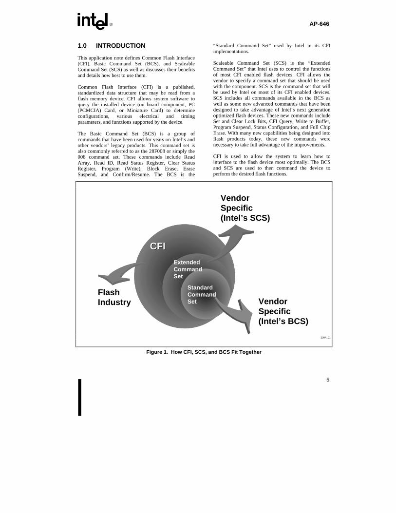
1.0 INTRODUCTION
This application note defines Common Flash Interface(CFI), Basic Command Set (BCS), and ScaleableCommand Set (SCS) as well as discusses their benefitsand details how best to use them.
Common Flash Interface (CFI) is a published,standardized data structure that may be read from aflash memory device. CFI allows system software toquery the installed device (on board component, PC(PCMCIA) Card, or Miniature Card) to determineconfigurations, various electrical and timingparameters, and functions supported by the device.
The Basic Command Set (BCS) is a group ofcommands that have been used for years on Intel’s andother vendors’ legacy products. This command set isalso commonly referred to as the 28F008 or simply the008 command set. These commands include ReadArray, Read ID, Read Status Register, Clear StatusRegister, Program (Write), Block Erase, EraseSuspend, and Confirm/Resume. The BCS is the
“Standard Command Set” used by Intel in its CFIimplementations.
Scaleable Command Set (SCS) is the “ExtendedCommand Set” that Intel uses to control the functionsof most CFI enabled flash devices. CFI allows thevendor to specify a command set that should be usedwith the component. SCS is the command set that willbe used by Intel on most of its CFI enabled devices.SCS includes all commands available in the BCS aswell as some new advanced commands that have beendesigned to take advantage of Intel’s next generationoptimized flash devices. These new commands includeSet and Clear Lock Bits, CFI Query, Write to Buffer,Program Suspend, Status Configuration, and Full ChipErase. With many new capabilities being designed intoflash products today, these new commands werenecessary to take full advantage of the improvements.
CFI is used to allow the system to learn how tointerface to the flash device most optimally. The BCSand SCS are used to then command the device toperform the desired flash functions.
FlashIndustry
CFICFI
ExtendedCommandSet
VendorSpecific(Intel’s SCS)
StandardCommandSet Vendor
Specific(Intel’s BCS)
2204_01
Figure 1. How CFI, SCS, and BCS Fit Together

AP-646 E
6
RemovableMedia
EmbeddedProducts
Future
Upgrade
Compatibility amongremovable media
Silicon updateswithout software
changes
Figure 2. CFI Allows Easy Upgrades and Use of Second Sources
2.0 BENEFITS OF CFI
The two primary benefits of using CFI are ease ofupgrading and second source availability. Both areconcerns when an OEM or end-user (the consumer)purchases a product.
2.1 Upgrades
In order to take advantage of increased densities (orspeeds, etc.) on memory devices and cards, an easyupgrade path is desirable. Care is generally taken toensure that hardware footprints are pin-for-pincompatible or that flexible layouts may be used whenupgrading a product. Thought is seldom given tosoftware compatibility, however. CFI allows many new
and improved products to be used in place of their olderversions without modifications of system software.
Because CFI allows the system to learn about thefeatures, parameters, and timings of a flash device, thesystem can take full advantage of these improvements.For instance, if the timeout for a block erase to occurwas cut in half, the system software could takeadvantage of that fact by changing its internal timers.Also, a 32-Mbit device can be replaced by a 64-Mbitdevice and vice versa because the device can tell thesystem what size it is.
With CFI, when upgrading a flash memory design, it isno longer necessary to re-optimize low level softwaredrivers to take advantage of the new features. Simplyprogram the system initially to accept CFI enableddevices, and allow the software to upgrade itself.
E AP-646
7
2.2 Second Sources
Particularly in the card environment, second sourcing isa primary concern. Because the end-user of a PC Card orMiniature Card could be a consumer, care must be takento ensure compatibility among all flash cards that maybe installed into the same sockets. For instance, whenpurchasing a replacement or spare memory card for theirdigital camera, a consumer does not want to have toworry that they can only purchase a certain vendor’scard or a particular version of what seems to be a similarcard.
This is analogous to a consumer purchasing floppy disksfor their computer or film for their camera. Any vendor’sproduct works. That is the goal of CFI—complete andsimple interchange between vendors in a cardapplication. The hardware inside the PC Card orMiniature Card does not have to operate identically; thesoftware takes care of the differences as long as thedevices are CFI-compliant.
CFI allows the system to determine the manufacturer ofthe card, its operating parameters, its configuration, andany special command codes that the card may accept.With this knowledge, the system can optimize its use ofthe card by using appropriate timeout values, optimalvoltages, and commands necessary to use the card to itsfull advantage.
3.0 HOW TO USE CFI EFFECTIVELY
To use CFI effectively, system software must be writtento take advantage of the flexibility provided by thespecification. The software must be capable ofmodifying timeouts, adjusting to different memory sizes,accommodating varying block erase characteristics, andbranching to vendor-specific code sections. Thefollowing paragraphs outline several steps which systemsoftware must transition through to read a CFI enableddevice. Flow charts are included in Appendix A1.
3.1 Read Query String
Not all devices installed into a flash memory socket willbe CFI-enabled. To determine if a device is CFI-capable,the system software must write a 98h to location 55hwithin the memory (see CFI Query Flowchart includedin Appendix A1). The flash device may or may not havean address sensitive query command; the Intel devicesdo not. The low-level driver, however, should supply the55h address even though the flash device may choose toignore the address bus and enter the query mode if 98his on the data bus only. If three consecutive maximum
device bus width reads beginning at location 10h in theflash array return the ASCII equivalent “Q,” “R,” and“Y,” then the device is CFI-compliant.
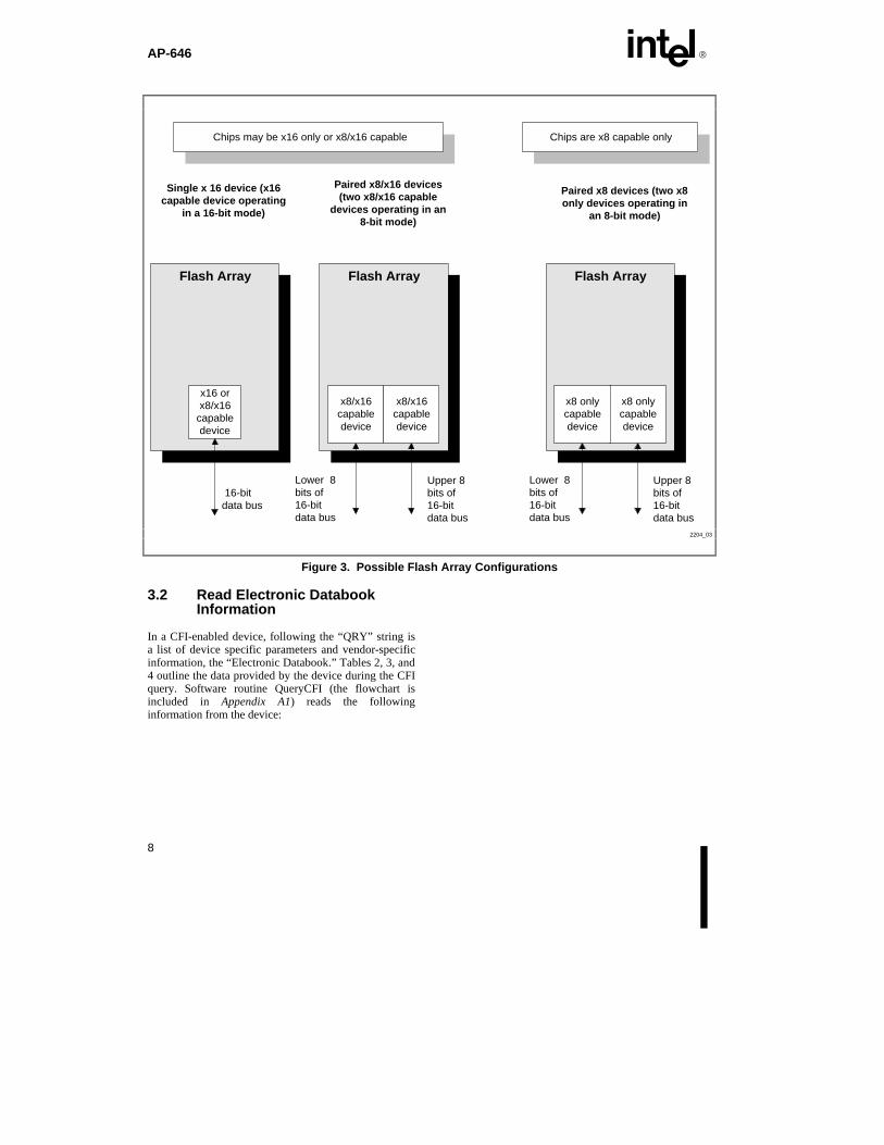
Although there are other configuration possibilities,there are currently three CFI array configurations thatare of primary interest. These configurations must betested for and accounted for in the software. Theseconfigurations are:
• single chip operating in a x16 mode (16-bit databus)—chips may be capable of 8 bit accesses, butare operating only with 16-bit bus accesses
• two chips each capable of 8- and 16-bit data busaccesses, but each only operating in a x8 mode (8-bit data bus on each chip with a total array buswidth of 16 bits)
• two chips each only capable of 8-bit data busaccesses operating only in a x8 mode (8-bit databus per chip with a total array bus width of 16 bits)
Each of these configurations are shown in Figure 3.Table 1 indicates the addressing necessary to read theCFI query table for each of these configurations alongwith some other possible device configurations. Thetable also includes what the query data will look like tothe host processor in byte or word addressing. Note thatthe query data (ASCII “Q”, “R”, and “Y” as well as theelectronic databook information discussed in the nextsection) may be doubled or even quadrupled dependingon the array configuration. The software must be able todetermine the correct array configuration based on thenumber of “Q”s returned to accurately calculate thearray size and read and write to the array properly. TheCFI Query Flowchart is located in Appendix A1. TheQueryCFI routine heuristically determines theconfiguration of the array, calculates the appropriatedata, and indicates to the higher level routines how tocommunicate with the CFI-enabled devices.
If the device does not respond with the “QRY” string,the device is not CFI-compliant and the software mustthen attempt to read the device’s JEDEC ID. (See theMemory Heuristics Flowchart included in Appendix A1.)The software must write a 90h to the first location in thedevice. If the device returns a Manufacturer’s ID andComponent ID, the flash device may be accessed as ithas been in the past, based on the Manufacturer andComponent ID. If the device does not return aManufacturer and Component ID, then the device is nota flash memory and other routines are necessary todetermine what type of device is installed. (See theMemory Heuristics Flowchart included in Appendix A1.)
AP-646 E
8
Chips are x8 capable onlyChips may be x16 only or x8/x16 capable
Single x 16 device (x16capable device operating
in a 16-bit mode)
Paired x8/x16 devices(two x8/x16 capable
devices operating in an8-bit mode)
Paired x8 devices (two x8only devices operating in
an 8-bit mode)
x16 orx8/x16
capabledevice
16-bitdata bus
Lower 8bits of16-bitdata bus
Upper 8bits of16-bitdata bus
Lower 8bits of16-bitdata bus
Upper 8bits of16-bitdata bus
Flash Array Flash Array Flash Array
x8/x16capabledevice
x8/x16capabledevice
x8 onlycapabledevice
x8 onlycapabledevice
2204_03
Figure 3. Possible Flash Array Configurations
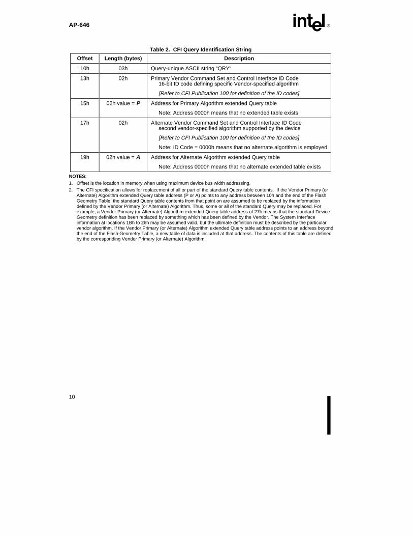
3.2 Read Electronic DatabookInformation
In a CFI-enabled device, following the “QRY” string isa list of device specific parameters and vendor-specificinformation, the “Electronic Databook.” Tables 2, 3, and4 outline the data provided by the device during the CFIquery. Software routine QueryCFI (the flowchart isincluded in Appendix A1) reads the followinginformation from the device:

E AP-646
9
s
Table 1. CFI Query Read
Device typeand data bus
operatingmode
Query start locationin maximum devicebuswidth addresses
Query data with maximumdevice buswidth
addressing(“x” = ASCII equivalent)
Query startaddress in
bytes
Query data withbyte addressing
x8 deviceoperating in 8bit mode
10h 10h: 51h “Q”11h: 52h “R”12h: 59h “Y”
10h 10h: 51h “Q”11h: 52h “R”12h: 59h “Y”
two x8devicesoperating in8 bit mode(paired chipconfiguration)
10h 10h: 0051h “Q”11h: 0052h “R”12h: 0059h “Y”
20h 20h: 51h “Q”21h: 51h “Q”22h: 52h “R”23h: 52h “R”24h: 59h “Y”25h: 59h “Y”
x16 deviceoperating in16 bit mode
10h 10h: 0051h “Q”11h: 0052h “R”12h: 0059h “Y”
20h 20h: 51h “Q”21h: 00h null22h: 52h “R”23h: 00h null
x16 deviceoperating in8 bit mode
N/A(1) N/A(1) 20h 20h: 51h “Q”21h: 51h “Q”22h: 52h “R”
two x16devicesoperating in8 bit mode(paired chipconfiguration)
N/A(1) N/A(1) 40h 40h: 51h “Q”41h: 51h “Q”42h: 51h “Q”43h: 51h “Q”44h: 52h “R”45h: 52h “R”
x32 deviceoperating in32 bit mode
10h 10h: 00000051h “Q”
11h: 00000052h “R”
12h: 00000059h “Y”
40h 40h: 51h “Q”41h: 00h null42h: 00h null43h: 00h null44h: 52h “R”
x32 deviceoperating in8 bit mode
N/A(1) N/A(1) 40h 40h: 51h “Q”41h: 51h “Q”42h: 51h “Q”43h: 51h “Q”44h: 52h “R”
NOTE:1. The system must drive the lowest order addresses to access all the device’s array data when the device is configured in x8
mode. Therefore, word addressing where these lower addresses not toggled by the system is “Not Applicable” for x8-configured devices.
AP-646 E
10
Table 2. CFI Query Identification String
Offset Length (bytes) Description
10h 03h Query-unique ASCII string “QRY“
13h 02h Primary Vendor Command Set and Control Interface ID Code16-bit ID code defining specific Vendor-specified algorithm
[Refer to CFI Publication 100 for definition of the ID codes]
15h 02h value = P Address for Primary Algorithm extended Query table
Note: Address 0000h means that no extended table exists
17h 02h Alternate Vendor Command Set and Control Interface ID Codesecond vendor-specified algorithm supported by the device
[Refer to CFI Publication 100 for definition of the ID codes]
Note: ID Code = 0000h means that no alternate algorithm is employed
19h 02h value = A Address for Alternate Algorithm extended Query table
Note: Address 0000h means that no alternate extended table exists
NOTES:1. Offset is the location in memory when using maximum device bus width addressing.
2. The CFI specification allows for replacement of all or part of the standard Query table contents. If the Vendor Primary (orAlternate) Algorithm extended Query table address (P or A) points to any address between 10h and the end of the FlashGeometry Table, the standard Query table contents from that point on are assumed to be replaced by the informationdefined by the Vendor Primary (or Alternate) Algorithm. Thus, some or all of the standard Query may be replaced. Forexample, a Vendor Primary (or Alternate) Algorithm extended Query table address of 27h means that the standard DeviceGeometry definition has been replaced by something which has been defined by the Vendor. The System Interfaceinformation at locations 1Bh to 26h may be assumed valid, but the ultimate definition must be described by the particularvendor algorithm. If the Vendor Primary (or Alternate) Algorithm extended Query table address points to an address beyondthe end of the Flash Geometry Table, a new table of data is included at that address. The contents of this table are definedby the corresponding Vendor Primary (or Alternate) Algorithm.

E AP-646
11
Table 3. System Interface Information
Offset Length(bytes)
Description
1Bh 01h VCC Logic Supply Minimum Program/Erase voltagebits 7–4 BCD value in voltsbits 3–0 BCD value in 100 millivolts
1Ch 01h VCC Logic Supply Maximum Program/Erase voltagebits 7–4 BCD value in voltsbits 3–0 BCD value in 100 millivolts
1Dh 01h VPP [Programming] Supply Minimum Program/Erase voltagebits 7–4 HEX value in voltsbits 3–0 BCD value in 100 millivolts
Note: This value must be 0000h if no VPP pin is present
1Eh 01h VPP [Programming] Supply Maximum Program/Erase voltagebits 7–4 HEX value in voltsbits 3–0 BCD value in 100 millivolts
Note: This value must be 0000h if no VPP pin is present
1Fh 01h Typical timeout per single byte/word write (buffer write count = 1), 2n µs
20h 01h Typical timeout for maximum-size buffer write, 2n µs(if supported; 00h = not supported)
21h 01h Typical timeout per individual block erase, 2n ms
22h 01h Typical timeout for full chip erase, 2n ms (if supported; 00h = not supported)
23h 01h Maximum timeout for byte/word write, 2n times typical (offset 1Fh)
24h 01h Maximum timeout for buffer write, 2n times typical (offset 20h)(00h = not supported)
25h 01h Maximum timeout per individual block erase, 2n times typical (offset 21h)
26h 01h Maximum timeout for chip erase, 2n times typical (offset 22h)(00h = not supported)

AP-646 E
12
Table 4. Flash Geometry Information
Offset Length(bytes)
Description
27h 01h Device Size = 2n in number of bytes.
28h 02h Flash Device Interface description [Refer to CFI Publication 100]
2Ah 02h Maximum number of bytes in buffer write = 2n.
2Ch 01h Number of Erase Block Regions within devicebits 7–0 = x = number of Erase Block Regions
Notes:1. x = 0 means no erase blocking, i.e., the device erases at once in “bulk.”
2. x specifies the number of regions within the device containing one or morecontiguous Erase Blocks of the same size. For example, a 128-KB device (1 Mb)having blocking of 16 KB, 8 KB, four 2 KB, two 16 KB, and one 64 KB isconsidered to have 5 Erase Block Regions. Even though two regions both contain16-KB blocks, the fact that they are not contiguous means they are separateErase Block Regions.
3. By definition, symmetrically- blocked devices have only one blocking region.
2Dh 04h Erase Block Region Information
bits 31–16 = z, where the Erase Block(s) within this Region are (z) times 256 bytes in size. The value z = 0 is used for 128-byte block size.e.g., for 64-KB block size, z = 0100h = 256 => 256 * 256 = 64K
bits 15– 0 = y, where y+1 = Number of Erase Blocks of identical size within the Erase Block Region:e.g., y = D15-D0 = FFFFh => y+1 = 64K blocks [maximum number]y = 0 means no blocking (# blocks = y+1 = “1 block”)
Note:y = 0 value must be used with # of block regions of one as indicated by (x) = 0
31h to(k-1)h
04h
perentry
Additional Erase Block Region Information, 4 bytes per region
Notes:
1. The total number of blocks times individual block size must add up to the devicesize.
2. The address K is next available Query address at end of the Device Geometrystructure. It is the first possible starting address of the optional vendor-specificQuery table(s) (i.e., Address “P,” the Primary Vendor-specific extended Querytable offset, must be ≥ k to not overwrite the existing tables). See note 2 underTable 2 for more information.
3.3 Read Vendor-Specific ExtendedQuery Table
Using data from addresses 15h (Address for PrimaryAlgorithm extended Query table) and possibly 19h(Address for Alternate Algorithm extended Query table),the system software can read more specific informationabout the flash device (see the CFI Query Flowchart,included in Appendix A1). Each vendor will havespecific data that should be read from the extended
query table. Intel defines this data with its SCS. Also,each vendor may locate this table in a different location,so it is important that the software reads the location ofthe tables from offsets 15h and 19h to determine where(if at all) the extended query data is stored. The VendorCommand Set definition (Intel’s SCS) will indicate whatdata is stored in the extended query table. Table 5 showsthe extended table for the Intel devices implementingCFI (all devices implementing CFI will use the extendedquery table regardless of the command set being used).

E AP-646
13
Table 5. Intel Primary Algorithm Extended Query Table
Offset Length(bytes)
Description
(P)h 03h Primary extended Query table unique ASCII string “PRI”
(P +3)h 01h Major version number, ASCII
(P +4)h 01h Minor version number, ASCII
(P +5)h 04h Optional Feature & Command Support
bit 0 Chip Erase Supported (1=yes, 0=no)bit 1 Suspend Erase Supported (1=yes, 0=no)bit 2 Suspend Program Supported (1=yes, 0=no)bit 3 Lock/Unlock Supported (1=yes, 0=no)bit 4 Queued Erase Supported (1=yes, 0=no)bits 5–31 Reserved for future use; undefined bits should be “0”
(P +9)h 01h Supported functions after Suspend
Read Array, Status, and Query are always supported during suspended Erase orProgram operation. This field defines other operations supported.
bit 0 Program supported after Erase Suspend (1=yes, 0=no)bits 1–7 Reserved for future use; undefined bits should be “0”
(P +A)h 02h Block Status Register Mask
Defines which bits in the Block Status Register section of Query are implemented.bit 0 Block Status Register Lock Bit [BSR.0] active (1=yes, 0=no)bit 1 Block Status Register Valid Bit [BSR.1] active (1=yes, 0=no)bits 2–15 Reserved for future use; undefined bits should be “0”
(P +C)h 01h VCC Logic Supply Optimum Program/Erase voltage (highest performance)bits 7–4 BCD value in voltsbits 3–0 BCD value in 100 millivolts
(P +D)h 01h VPP [Programming] Supply Optimum Program/Erase voltagebits 7–4 HEX value in voltsbits 3–0 BCD value in 100 millivolts
Note: This value must be 0000h if no Vpp pin is present
(P +E)h reserved Reserved for future versions of the SCS Specification
AP-646 E
14
3.4 Software Branch to AppropriateRoutines
Using the information read from location 13h (PrimaryVendor Command Set and Control Interface ID code)and possibly from 17h (Alternate Vendor Command Setand Control Interface ID Code), the system determineswhich set(s) of commands are recognizable by the flashdevice. Every vendor has defined at least one set ofcommands that their flash devices accept. Anycommands other than those defined will either berejected or cause unexpected behavior and shouldtherefore be avoided.
Intel has two such sets of commands defined, BCS(Basic Command Set) and SCS (Scaleable CommandSet). SCS includes all of the BCS commands plus somenew enhanced ones. The low level reference codeprovided by Intel includes both of these command sets.By using this reference code, current and future flashdevices may be controlled using the same systemsoftware drivers.
4.0 HOW TO USE COMMAND SETSEFFECTIVELY
Flowcharts for most of the driver software routinesnecessary to implement the Basic and ScaleableCommand Sets are located in Appendix A2 and A3respectively. All of the reference code may bedownloaded from the Intel web site from the electronictools catalog. To ensure compatibility with future CFIcompliant devices, all functions of the reference codeshould be included in a design.
5.0 CONCLUSION
CFI and SCS have been created to allow a systemdesigner the flexibility to design products now that canuse both current and future flash memory devices aswell as the security of knowing that second sourceproducts may be used without system softwaremodifications.

E AP-646
15
APPENDIX AFLOWCHARTS
A1 MEMORY HUERISTICS
A1.1 Memory Hueristics Flowchart
Read and Store Data fromDevice Address 0
Start
Issue Read JEDEC IDWrite 90h to Address 0h
Data =“QRY”?
Issue CFI QueryWrite 98h to Address 55h
Read CFI Parameters fromDevice (See CFI Query)
Data at 0= 90h?
Restore Original Data
Return, SRAM Device
Return, CFI Device
ReadIDs?
Issue AMD Read JEDEC ID,Write AA55h to Address 0h
ReadIDs?
Yes
No
No
No
Yes
Yes
Yes
Load Software RoutineAddresses from Tables
Return, ROM Device
No
Determine Size of RAM Load Software RoutineAddresses from Tables
Read JEDEC parameters fromSystem Table
(See JEDEC Query)Return, JEDEC Flash Device
2204_03

AP-646 E
16
A1.2 CFI Query Flowchart
Issue CFI Query,to address 55h
Return, CFI Device
Start
BusOperation
Command Comments
Write CFI Query Data = 98hAddr = 55h
Read ASCII Q, R, and YRead Block SizeRead Number of Erase RegionsRead Device SizeRead Max Write Buffer SizeRead Max and Typical Voltages and
TimeoutsRead Address of Extended TableRead Features SupportedWrite CFI Query Data = 98h
Addr = 55hRead ASCII Q, R, YWrite Read Array Data = FFh
Addr =X
Read Number of Erase Regions
Read Device Size
Paired
x8?
Read Max Write Buffer Size
Read Max and TypicalVoltages and Timeouts
Read Address of ExtendedQuery Table
Determine Features Supportedby Device
Map to Next Flash Device
Read Erase Block Size
Return, Non-CFI Device
No
Yes
Paired
x8/x16?
Single
x16?
No No
YesYes
Data =QRY?
Issue CFI Query Command toAddress 55h
Data =QRY? Put Device into Read Array
Mode, Write FFh
Put Device into Read ArrayMode, Write FFh
No
Yes
No
Yes
2204_04

E AP-646
17
A1.3 Read JEDEC ID Flowchart
Return, JEDEC Flash Device
Load geometric parameters fromSoftware Tables
Load Software RoutineAddresses from Tables
Map in Next Flash Device
Return, Unknown Device
JEDEC IDin Table?
JEDEC ID?
Issue Read JEDEC IDCommand (90h)
JEDEC ID?Issue Read Array Command
(FFh)
Issue Read Array Command(FFh)
Issue Read ID,Write 90h to Address 0
Start BusOperation
Command Comments
Write Read ID Data = 90hAddr = 0
Read Data = Manufacturer IDAddr = 0
Read Data = Device IDAddr = 1
Write Read ID Data = 90hAddr = 0
Write Read Array Data = FFhAddr = X
Read Location 0 and 1in Flash Array (Manufacturer
and Device ID)
2204_05

AP-646 E
18
A2 BASIC COMMAND SET
A2.1 Clear Status Register Flowchart
Issue Clear SR CommandWrite 50H
Status Register Cleared
Start BusOperation
Command Comments
Write Clear StatusRegister
Data = 50hAddr = X
2204_06

E AP-646
19
A2.2 Read Array Flowchart
Issue Read ArrayWrite FFh
Return, Data Read
Start BusOperation
Command Comments
Write Read Array Data = FFhAddr = Address to read
Standby Check SR.71 = WSM ready0 = WSM busy
Read Read array locations
Read Array Data
DoneReading?
No
Yes
Verify Write Size < Device Size
Read Status Register
SR.7 = ?
Call Suspend Routine
1
0
Need toResume?
Call Resume Routine
Return, Data Read
No
Yes
2204_07

AP-646 E
20
A2.3 Block Erase Flowchart
DeviceSupportsQueuing?
No
Yes
Set Timeout
Issue Block Queue EraseCommand 28h and Block
Address
Start
Read Extended Status Register
Is QueueAvailable?
XSR.7=
EraseBlock
Timeout?
No
= 0, No
= 1, Yes
AnotherBlock
Erase?
Issue Block Queue EraseCommand 28h and Block
Address
Read Extended Status Register
Is QueueAvailable?
XSR.7=
= 0, No
= 1, Yes
Write Confirm D0h and BlockAddress
No
Yes
AnotherBlock
Erase?
Yes
No
Read Status Register
SR.7= ?
Full Status Check if Desired
Erase Flash Block(s)Complete
Issue Single Block EraseCommand 20h and Block
Address
Write Confirm D0h and BlockAddress
SuspendEraseLoop
0
1
BusOperation
Command Comments
Write Erase Block Data = 28h or 20hAddr = Block Address
Read XSR.7 = validAddr = X
Standby Check XSR.71 = Erase queue available0 = No Erase queue available
Write Erase Block Data = 28hAddr = Block Address
Read SR.7 = valid; SR.6-0 = XCE# and OE# low updates SRAddr = X
Standby Check XSR.71 = Erase queue available0 = No erase queue available
Write(Note 1)
EraseConfirm
Data = D0hAddr = X
Read Status Register dataCE# and OE# low updates SRAddr = X
Standby Check SR.71 = WSM ready 0 = WSM busy
1. The Erase Confirm byte must follow Erase setup when theerase queue status (XSR.7) = 0.Full status check can be done after all Erase and Programsequences complete. Write FFh after the last operation toreset the device to read array mode.
Yes
2204_08

E AP-646
21
A2.4 Erase Suspend/Resume Flowchart
SR.7 =0
1
ReadStatus Register
Issue Suspend CommandWrite B0H
Erase Resumed
Start
SR.6 =0
1
Erase Complete
Done?No
Yes
Read Array Data,Read SR, or Write Data
Issue Read or WriteCommand
Issue Resume command,Write D0h
Return, Nothing to Suspend
Issue Read Command,Write FFh
BusOperation
Command Comments
Write EraseSuspend
Data = B0hAddr = X
Read SR.7=valid; SR.6-0=XCE# & OE# low updates SRAddr = X
Standby Check SR.71 = WSM ready0 = WSM busy
Standby Check SR.61 = Erase suspended0 = Erase in progress or complete
Write Read Array,Read SR, or
Write
Data = FFhAddr = X
Read/Write Read/Write array locations otherthan those being erased or Read SR
Write Resume Data = D0hAddr = X
2204_09

AP-646 E
22
A2.5 Single Byte Program (Write) Flowchart
SR.7 =0
1
Write Data to Address
Issue Program Command, 40hor 10h and Address
Start
ReadStatus Register
Full Status Check if Desired
Byte / Word ProgramComplete
BusOperation
Command Comments
Write Setup Byte /WordProgram
Data = 40h or 10hAddr = Location to Be Programmed
Write Byte / WordProgram
Data = Data to Be ProgrammedAddr = Location to be Programmed
Read Status Register DataStandby Check SR.7
1 = WSM Ready0 = WSM Busy
Repeat for subsequent program operations.Full status register check can be done after each programoperation or after a sequence of Programming.Write FFh after the last program operation to place the device inread array mode.
2204_10

E AP-646
23
A2.6 Full Status Check Flowchart
Start
SR.1 =
0
1
SR.2 =
0
1
SR.4 =
0
1
SR.3 =
0
1
Device Protect Error
Write Is Suspended
Voltage Range Error
Write or Block Lock Bit SetError
BusOperation
Command Comments
Standby Check SR.31 = Programming Voltage Error Detect
Standby Check SR.11 = Device Protect Detect
Standby Check SR.4,5Both 1 = Command Sequence Error
Standby Check SR.51 = Clear Block Lock-Bits Error
SR.5, SR.4, SR.3, and SR.1 are only cleared by the Clear Status Register command.If error is detected, clear the status register before attempting retry or other error recovery.
SR.5 =1
0
Clear Block Lock Bit or EraseError
SR.6 =1
0
Erase Suspended
SR.4, 5 =1
0
Command Sequence Error
Read Status Register
Return, Status Checked
2204_11

AP-646 E
24
A3 SCALEABLE COMMAND SET
A3.1 Write to Buffer Flowchart
XSR.7 =
1
Issue Write Command E8h andBlock Address
Set Timeout
Start
Read Extended Status Register
Write BufferTimeout?
0
No
Write Buffer Data and StartAddress
Write Word or Byte Count andBlock Address
X = 0
X = N ?
Abort BufferWrite
Command?
No
X = X + 1
Write Next Buffer Data andDevice Address
Buffer Write to Flash ConfirmD0h
No
Yes
Write to Another Block Address
Buffer Write to Flash Aborted
AnotherBufferWrite?
Yes
No
BusOperation
Command Comments
Write Write toBuffer
Data = E8hAddr = Block Address
Read XSR.7 = valid; XSR.6-0 = X;Addr = X
Standby Check XSR.71 = Write buffer ready0 = No write buffer ready
Write(Notes 1,2)
Data = N = word/byte countN = 0 corresponds to count = 1Addr = Block Address
Write(Notes 3,4)
Data = write buffer dataAddr = device address
Write(Notes 5.6)
Data = write buffer dataAddr = device address
Write WriteConfirm
Data - D0hAddr = X
Read Status Register DataCE# and OE# low updates SRAddr = X
Standby Check SR.71 = WSM ready0 = WSM busy
1. Byte/word count values on DQ0-7 are loaded into the count register.2. The device now outputs the status register when read (XSR is no longeravailable).3. Write Buffer contents will be programmed at the device start address ordestination flash address.4. Align the start address on a Write Buffer boundary for maximumprogramming performance.5. The device aborts the Write to Buffer command if the current address isoutside of the original block address.6. The status register indicates an “improper command sequence” if theWrite to Buffer command is aborted. Follow this with a Clear StatusRegister command.
Full status check can be done after all Erase and Write sequencescomplete. Write FFh after the last operation to reset the device to readarray mode.
Issue Read Status Command
Read Status Register
SR.7 =0
1
Full Status Check if Desired
Buffer Write to FlashComplete
SuspendWrite Loop
Yes
Yes
2204_12

E AP-646
25
A3.2 Program (Write) Suspend/Resume Flowchart
SR.7 =0
1
ReadStatus Register
Issue Suspend CommandWrite B0h
Write Resumed
Start
SR.2 =0
1
Write Complete
DoneReading?
No
Yes
ReadArray Data
Issue Read CommandWrite FFh
Issue Resume commandWrite D0h
Return, Nothing to Suspend
Issue Read CommandWrite FFh
BusOperation
Command Comments
Write Write Suspend Data = B0hAddr = X
Read SR.7=valid; SR.6-0=XCE# & OE# low updates SRAddr = X
Standby Check SR.71 = WSM ready0 = WSM busy
Standby Check SR.21 = Write suspended0 = Write complete
Write Read Array Data = FFhAddr = X
Read Read array locations other thanthose being written
Write Resume Data = D0hAddr = X
2204_13

AP-646 E
26
A3.3 Block Lock Bit Set Flowchart
ReadStatus Register
Write 60h,Block Address
Start
SR.7 =0
1
Issue Read CommandWrite FFh
Write 01h,Block Address
Set Lock-BitComplete
BusOperation
Command Comments
Write Set Block Lock-BitSetup
Data = 60hAddr = Block Address (Block)
Write Set BlockLock-Bit Confirm
Data = 01hAddr = Block Address (Block)
Read Status Register Data
Standby Check SR.71 = WSM Ready0 = WSM Busy
Repeat for subsequent lock-bit set operations.Full status check can be done after each lock-bit set operation or after a sequence of lock-bit set operations.Write FFh after the last lock-bit set operation to place device in read array mode.
Full Status Check if Desired
2204_14
A3.4 Block Lock Bit Reset Flowchart
Read StatusRegister
Write 60h
Start
SR.7 =0
1
Full StatusCheck if Desired
Write D0
Clear Block Lock-BitsComplete
BusOperation
Command Comments
Write Clear BlockLock-Bits Setup
Data = 60hAddr = X
Write Clear BlockLock-Bit Confirm
Data = DOhAddr = X
Read Status Register Data
Standby Check SR.71 = WSM Ready0 = WSM Busy
Write FFh after the last lock-bit set operation to place device in read array mode.
2204_15