colorless onu with discolored source and hybrid soi integrated wavelength converter
TRANSCRIPT
386 IEEE PHOTONICS TECHNOLOGY LETTERS, VOL. 24, NO. 5, MARCH 1, 2012
Colorless ONU With Discolored Source andHybrid SOI Integrated Wavelength Converter
Ioannis Lazarou, Christos Stamatiadis, Bernhard Schrenk, Leontios Stampoulidis, Lars Zimmermann,Karsten Voigt, Giovan Battista Preve, Ludwig Moerl, Jochen Kreissl, and Hercules Avramopoulos
Abstract— We present a novel optical network unit (ONU)featuring a “colorless” directly modulated laser (DML) enabledby a hybridly integrated all-optical wavelength converter(AOWC), supporting operation beyond 10 Gb/s. It incorporatesa semiconductor optical amplifier (SOA) for wavelength conver-sion and two cascaded delay interferometers (DIs) for spectralprocessing. The ONU was proven at full duplex 10-Gb/s datarate in a WDM passive optical network.
Index Terms— Fiber-to-the-home (FTTH), optical access,optical communication terminals, wavelength conversion (WC).
I. INTRODUCTION
COLORLESS WDM has been considered a key technol-ogy for enabling broadband services to the user. So
far, colored equipment applied in present FTTH communi-cation equipment has prohibited a smooth upgrade towardsNG-PON2. On the contrary, WDM-PONs employing wave-length independent ONUs are now being investigated asnetwork topologies with simple administration, maintenancerequirements and low operational expenses [1]. The overallimplementation relies on “colorless” concepts, in which wave-length channel generation and control are kept in the centraloffice, while wavelength agnostic remote US modulation isapplied at customer premises. Until now, one of the firstdemonstrations of colorless ONUs has been implementedwith a reflective SOA (RSOA), which offers data rates upto 10 Gb/s, but with a trade-off between the gain andbandwidth that limits its operational speed. An alternativepath is to recycle colored customer equipment for colorlessWDM/XDM-PON environments exploiting WC procedures.
Manuscript received October 19, 2011; revised November 24, 2011;accepted December 7, 2011. Date of publication December 13, 2011; dateof current version February 15, 2012. This work was supported in part by theEuropean FP7 BOOM Project.
I. Lazarou, C. Stamatiadis, B. Schrenk, and H. Avramopoulos are withthe School of Electrical and Computer Engineering, National TechnologicalUniversity of Athens, Athens 15780, Greece (e-mail: [email protected];[email protected]; [email protected]; [email protected]).
L. Stampoulidis is with Constelex Technology Enablers, Corallia Microelec-tronics Innovation Center, Athens 15125, Greece (e-mail: [email protected]).
L. Zimmermann is with Technische Universität Berlin, Joint Lab-oratory Silicon Photonics HFT4, Berlin 10587, Germany, and alsowith IHP GmbH, Frankfurt/Oder, Frankfurt 15236, Germany (e-mail:[email protected]).
K. Voigt is with Joint Laboratory Silicon Photonics HFT4, Technische Uni-versität Berlin, Berlin 10587, Germany (e-mail: [email protected]).
G. B. Preve is with Nanophotonics Technology Center, Universidad Politec-nica de Valencia, Valencia 46022, Spain (e-mail: [email protected]).
L. Moerl and J. Kreissl are with Fraunhofer-Institut für Nachrichten-technik, Heinrich-Hertz-Institut, Berlin 10587, Germany (e-mail:[email protected]; [email protected]).
Color versions of one or more of the figures in this letter are availableonline at http://ieeexplore.ieee.org.
Digital Object Identifier 10.1109/LPT.2011.2179644
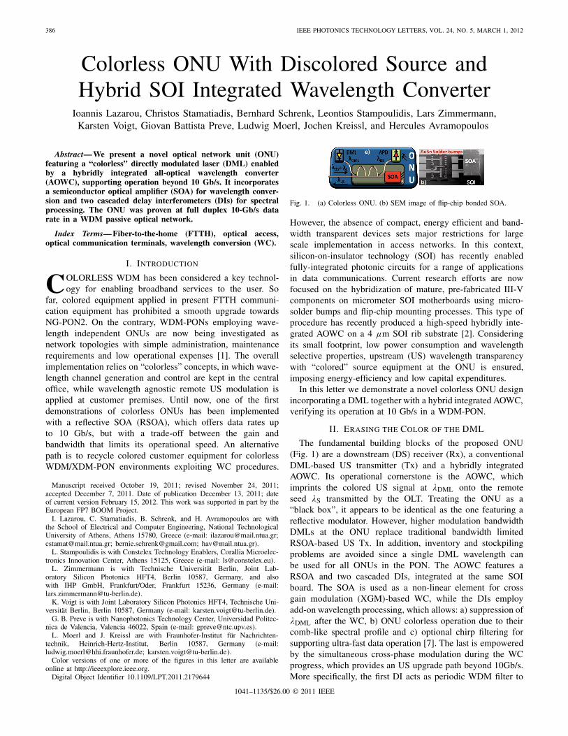
Fig. 1. (a) Colorless ONU. (b) SEM image of flip-chip bonded SOA.
However, the absence of compact, energy efficient and band-width transparent devices sets major restrictions for largescale implementation in access networks. In this context,silicon-on-insulator technology (SOI) has recently enabledfully-integrated photonic circuits for a range of applicationsin data communications. Current research efforts are nowfocused on the hybridization of mature, pre-fabricated III-Vcomponents on micrometer SOI motherboards using micro-solder bumps and flip-chip mounting processes. This type ofprocedure has recently produced a high-speed hybridly inte-grated AOWC on a 4 μm SOI rib substrate [2]. Consideringits small footprint, low power consumption and wavelengthselective properties, upstream (US) wavelength transparencywith “colored” source equipment at the ONU is ensured,imposing energy-efficiency and low capital expenditures.
In this letter we demonstrate a novel colorless ONU designincorporating a DML together with a hybrid integrated AOWC,verifying its operation at 10 Gb/s in a WDM-PON.
II. ERASING THE COLOR OF THE DML
The fundamental building blocks of the proposed ONU(Fig. 1) are a downstream (DS) receiver (Rx), a conventionalDML-based US transmitter (Tx) and a hybridly integratedAOWC. Its operational cornerstone is the AOWC, whichimprints the colored US signal at λDML onto the remoteseed λS transmitted by the OLT. Treating the ONU as a“black box”, it appears to be identical as the one featuring areflective modulator. However, higher modulation bandwidthDMLs at the ONU replace traditional bandwidth limitedRSOA-based US Tx. In addition, inventory and stockpilingproblems are avoided since a single DML wavelength canbe used for all ONUs in the PON. The AOWC features aRSOA and two cascaded DIs, integrated at the same SOIboard. The SOA is used as a non-linear element for crossgain modulation (XGM)-based WC, while the DIs employadd-on wavelength processing, which allows: a) suppression ofλDML after the WC, b) ONU colorless operation due to theircomb-like spectral profile and c) optional chirp filtering forsupporting ultra-fast data operation [7]. The last is empoweredby the simultaneous cross-phase modulation during the WCprogress, which provides an US upgrade path beyond 10Gb/s.More specifically, the first DI acts as periodic WDM filter to
1041–1135/$26.00 © 2011 IEEE

LAZAROU et al.: COLORLESS ONU WITH DISCOLORED SOURCE AND HYBRID SOI INTEGRATED WAVELENGTH CONVERTER 387
LD
LD
MZ
M
EDFA
PIN
PC
TxRx
EDFA
EDFA
SMF8.2/25 km
SMF800 m
8.2/25 kmPON loss budgetD
95%
5%
A B(a)
AU
AS
AD
DI DISOA
SOA 40 mA35 mA
30 mA
Modulation frequency [GHz]0 1 2 3 4 5 6 7 8 9 10 11 12
−12
−9
−6
−3
0(d)
E/O
res
pons
e [d
B]
PC
Tx
2nd DI
1st DI(b)
(c)a
a aPowermon.
OLT
OBPF
OBPFS
OADF
DMLRxONUλS
λDS
Fig. 2. (a) Experimental proof-of-concept setup. (b) AOWC photonic chip. (c) DML. (d) DML electro-optical (e/o) response for different bias currents.
0
−10
−20
−30
0−10−20−30−40−50
0
−20
−40
−600
−10−20−30−40−50
(a)
(c) (d)
(b)
WC-USDML
λUS
λDML
Wavelength [nm]
Nor
mal
ized
out
put p
ower
[dB
]
1550.1 1550.6 1551.1 1547 1547.5 1548
1530 1540 1550 1560 1546 1548 1550 1552
Fig. 3. Spectra of (a) cascaded DI response in case of ASE injection,(b) output of AOWC, (c) WC US, and (d) DML output.
interleave the US at λDML with the seed at λS, whereas thesecond one acts as an additional filter for obtaining spectralresponses with higher outband suppression allowing to dropthe DS at the same time.
Since no RSOA was available, the concept was validatedwith a proof-of-principle ONU, having a two-port hybrid inte-grated AOWC. The device employs a prefabricated 1.25mmnon linear SOA and two cascaded DIs (Fig. 2b). A buriedheterostructure with p-n current blocking layers is flip-chipadapted on the SOI motherboard with 14 μm AuSn bumps.Laterally tapered in/output waveguides act as spot-size con-verters. For proper horizontal and vertical optical adjustment,alignment marks and dry etched trenches are implemented ascounterparts to the SOI board stand-offs. The motherboardincorporates an integration zone forming a landing site forthe SOA. The SOA mounting on the SOI substrate is beingperformed by a high accuracy flip-chip bonder (1 μm preci-sion) taking over the positioning against the stand-offs and thethermal cycling for bump reflow soldering. The AOWC hada fiber-to-fiber loss of ∼20dB due to the 3 μm x-axis offsetmisalignment between the SOA facet and the SOI waveguide,which can be further reduced after a series of flip-chip attemptsand high-level optimization towards to a placement accuracydown to submicron level. The cascaded DIs have a FreeSpectral Range (FSR) of 5.6nm and 2.52nm and their optionalfull FSR tuning is accomplished by two independently tunedon-chip thermal heaters.
III. EXPERIMENTAL VALIDATION IN WDM-PON
The proposed ONU was proven in a WDM-PON setup(Fig. 2a) at 10Gb/s full-duplex transmission. The OLT dis-tributes together with the 10Gb/s modulated DS signalat λDS = 1543.67nm an unmodulated seed wavelength atλS = 1550.3nm with 13dBm total power and an optical signal-to-noise-ratio (OSNR) of 47dB (λS) and 42.9dB (λDS) respec-tively. The optical distribution network was composed by adual feeder fiber link with lengths of 8.2 or 24.2km of standard
single mode fiber (SSMF) and a short drop fiber of 800m.The PON wavelength distributing element was considered tobe a cyclic AWG and was emulated by two tunable 1nmoptical bandpass filters and two 3dB couplers. The loss budget,defined between the OLT and the ONU, was fixed to 20dBfor both transmission directions by attenuators (AS, AU). Atthe ONU, a Red/Blue optical add/drop filter (OADF), thatcan be in principle functionally integrated in the DI cascade,separates λDS and λS. The former is detected with a PIN+TIAcombination. The ONU-Tx employs a packaged DML with abandwidth of 6.7GHz when biased at 35mA (Fig. 2d), emittingat λDML = 1547.36 nm. Then, both the seed at λS and the USdata at λDML were combined and co-injected into the AOWC.The high chip losses were compensated by two EDFAs beforeand after the AOWC. The ONU output power and OSNRwere 1dBm and 34.6dB, respectively. Due to the 60nm 3-dBbandwidth of the SOA at its bias current of 140mA, WC canbe accomplished for the whole WDM-PON spectrum. Further-more, the fast SOA recovery time (�t10−90) of ∼30ps enablesWC at high data rates beyond current access standards. Thewavelength-translated US is then received at the OLT on itsdesignated wavelength λS by an EDFA+PIN-based receiver.
IV. RESULTS AND DISCUSSION
The normalized spectra of the periodic response of the DIs,the AOWC output, the WC-US (λS) and the DML output(λDML) are presented at Fig. 3(a-d). As can be noticed, theDIs biasing was not performed, since both λS and λDMLwere adjusted to fit with a peak and a notch of the DIs. Forthe bit-error ratio (BER) measurements (Fig. 4a-f), variableattenuators (AD , AU ) were placed in front of the DS and USRx. Figure 4a) depicts the B2B BER curves of the DML-USfor different data-rates. Error floors (EF) at 3.10−7 and 2.10−4
are observed for bit-rates of 10 and 12Gb/s, respectively, due tothe bandwidth limitation of the DML (Fig. 2c). A lower rate of7.5Gb/s improves the sensitivity by 6dB at the Reed Solomon(255, 239) forward error correction (FEC) threshold. Figure 4bshows the transmission results of the direct DML-US overdifferent feeder lengths for a fixed data rate of 10 Gb/s. A lowBER of 10−10 was achieved over 9km, improving the powermargin by 4.7dB at the FEC level with respect to the B2Bcase. As explained in [3], a slight offset filtering at OLT-Rxand the broadening of the chirped DML pulses, caused bythe dispersion, leads to a significant overshoot reduction atthe their trailing edges. Hence, the overall DML performanceis improved. Increasing the PON reach at 25km, the pulsedispersion dominates and an EF is noted at a level of 2.3 10−3.
Figure 4c) depicts the BER curves referring to theWC-US. Unlike the EF of the 10G/s B2B DML-US, a lower

388 IEEE PHOTONICS TECHNOLOGY LETTERS, VOL. 24, NO. 5, MARCH 1, 2012
−2
−3
−4
−5−6−7−8−9−10
(a) (b)
(d)(e)
6 dB
RS (255,239) FEC Threshold
OLT Rx input power [dBm]lo
g (D
ML
BE
R)
−2
−3
−4
−5
−6
−7
−8
−9
−3
−4
−5
−6
−7−8−9
−10
5
4
3
2
1
0
−1
−2
log
(WC
-US
BE
R)
log
(DS
BE
R)
Pena
ltv [
dB]
−34 −31 −28 −25 −22 −19
PON reach [km]0 5 10 15 20 25
Wavelength [nm]1540 1545 1550 1555 1560
EDFAgain
roll-off
(f)(g)
ONU-Rx input power [dBm]−31 −30 −29 −28
−
−27 −26 −25
DMLbias
Acc
umul
ated
pow
er c
onsu
mpt
ion
[W] 1.8
1.6
1.4
1.2
1
0.8
0.6
0.4
0.2
0
DML+AOWS
10 Gb/SRSOA
DMLdrive
RF
driv
eE
qual
izer
loss
TE
CW
Cbi
as
DC
bias
81521
121824
Optical US lossbudget [dB]
10 Gb/s B2B DML12.5 Gb/s B2B DML7.5 Gb/s B2B DML
−3
−4
−5
−6
−7
−8−9−10
(c)
RS (255,239) FECThreshold
OLT Rx input power [dBm]
log
(Wc-
US
BE
R)
−26 −23 −17−20 −14 −11 −7−8
10 Gb/s WC-US:B2B10 Gb/s WC-US:9 km12 Gb/s WC-US:B2B
−2
−3
−4
−5−6−7−8−9−10
4.7 dB
OLT Rx input power [dBm]
log
(DM
L B
ER
)
−33 −30 −27 −24 −21 −15−18
10 Gb/s DML-B2B10 Gb/s DML-9 km SMF10 Gb/s DML-25 km SMF
10 Gb/s DS-B2B10 Gb/s DS-9 km SMF10 Gb/s DS-25 km SMF
Fig. 4. (a) and (b) BER for DML-US in (a) B2B and different rates and (b) transmission at 10 Gb/s. (c)–(e) BER for WC-US at (c) different rates, (d) differentPON reach, and (e) for colorless operation. (f) BER for DS at 10 Gb/s. (g) Power consumption comparison for the AOWC- and a RSOA-based ONU.
BER of 4.10−10 can be accomplished in case of the WC. Thisis mainly attributed at the gain dynamics of the SOA, when itis operated at deep saturation. The injected pulses from DMLlead to carrier depletion and, consequently, overshoots at thetrailing bit edges are gain suppressed. Thus, the SOA actsas a power limiter and pulse-shaper circuit [4]. Therefore,the XGM-based WC to a co-propagating seed signal is notaffected by transient amplitude fluctuations as it is the casefor the DML without WC, due to the 2R regenerative behaviorof the AOWC. Also, by further increasing the DML data rateto 12Gb/s, the WC-US shows a comparably decreased EF at5.10−5, at which a penalized reception is still possible. AtFig. 4d) the US performance exploiting the AOWC is shownfor different PON reach as function of the loss budget. US lossbudgets of up to the targeted 20dB are compatible with a reachof ∼18km. As prementioned, the curves’ dip noticed at ∼9kmstems from the offset filtering performed at the OLT-Rx.
The colorless ONU operation was validated under differ-ent OLT seed wavelengths λS, which were centered at theperiodic peaks of the cascaded DI response. By maintainingthe B2B BER curve for λS = 1550.3nm as reference, indicantB2B BER points for four additional seed wavelengths wereacquired. As indicated in Fig. 4e), the power penalties withrespect to the original 1550.3nm wavelength are ranging+/−2dB. This is mainly attributed to the SOA gain profile aswell as to the non-uniform spectral response of the DIs. Theextra-ordinary high penalty observed for 1557nm operationderives from the limited operational area of the EDFAs andthe degraded WC efficiency occurring for far detuned wave-lengths. Figure 4f) presents the BER performance of the DS.Transmission at 10 Gb/s over 9 and 25km shows a penaltyof <1dB at a BER of 10−10 with respect to the B2B case.A budget beyond 30dB is suitable for the DS, leaving apower margin of ∼15dB without FEC. Table I summarizesthe compatible PON loss budgets in case of FEC at the Rx.As the smallest, the seed loss budget imposes a limitation to18dB at the overall budget.
Finally, the power consumption of the proposed AOWC-based ONU and an equivalent 10Gb/s RSOA-based ONU [5]was investigated (Fig. 4g). In a direct comparison betweenthe modulators, the DML benefits from its 4.6-fold lowerbias and RF drive with respect to the RSOA. Moreover, thelarger intrinsic e/o modulation bandwidth of the DML enables
TABLE I
COMPATIBLE PON LOSS BUDGETS FOR B2B CASE AND FEC
Stream/seed
Tx power[dBm]
Rx Sens./ONUInput [dBm] Loss budget [dB]
DS 10 −29.8 39.8US 0 −23.6 . . . − 19.6 23.6 …19.6CW 10 −8 18
Compatible loss budget [dB]: 18
operation without extra equalizing RF circuitry. The latteraffects the power consumption of the RSOA negatively dueto the excess RF drive needed to compensate the losses ofthe passive equalizer [5]. Despite the need for a temperaturecontroller for the current version of the AOWC, the validatedONU needs ∼400mW less power compared to the equivalent
RSOA-based ONU scheme. Further improvement can beobtained with uncooled AlGalnAs SOAs for the AOWC [6].
V. CONCLUSION
An upgrade from colored to colorless ONUs using a SOIhybrid AOWC was presented. The photonic chip performsXGM-based WC with 2R regenerative properties and spec-tral processing with a SOA and a DI cascade, respectively.Optional chirp filtering exploitation can increase US data-rate.
REFERENCES
[1] M. Maier, “WDM passive optical networks and beyond: The roadahead,” J. Opt. Commun. Netw., vol. 1, no. 4, pp. C1–C16, 2009.
[2] L. Zimmermann, et al., “High-precision flip-chip technology for allop-tical wavelength conversion using SOI photonic circuit,” in Proc. GroupIV Photon., London, U.K., Sep. 2011, pp. 237–239, paper P2.4.
[3] I. Papagiannakis, D. Klonidis, A. Birbas, J. Kikidis, and I. Tomkos,“Performance improvement of low-cost 2.5-Gb/s rated DML sourcesoperated at 10 Gb/s,” IEEE Photon. Technol. Lett., vol. 20, no. 23, pp.1983–1985, Dec. 1, 2008.
[4] N. Pleros, G. T. Kannelos, C. Bintjas, A. Hatziefremidis, and H.Avramopoulos, “Optical power limiter using a saturated SOA-basedinterferometric switch,” IEEE Photon. Technol. Lett., vol. 16, no. 10,pp. 2350–2352, Oct. 15, 2004.
[5] B. Schrenk, G. de Valicourt, M. Omella, J. A. Lazaro, R. Brenot, andJ. Prat, “Direct 10-Gb/s modulation of a single-section RSOA in PONswith high optical budget,” IEEE Photon. Technol. Lett., vol. 22, no. 6,pp. 392–394, Mar. 15, 2010.
[6] S. Tanaka, A. Uetake, S. Okumura, M. Ekawa, G. Nakagawa, andK. Morito, “Uncooled, polarization-insensitive AlGalnAs MQW-SOAmodule operable up to 75 °C with constant current,” in Proc. ECOC’11,Geneva, Switzerland, Sep., pp. 1–3, paper Tu.6.LeSaleve.2.
[7] F. Gomez-Agis, et al., “All-optical wavelength conversion at 160 Gbit/susing SOA and silicon-on-insulator photonic circuit,” Electron. Lett.,vol. 45, no. 22, pp. 1132–1133, Oct. 15, 2009.