cmos terahertz integrated circuits and systemssscs.ieee.org/images/files/forwebsite.pdf · psi...
TRANSCRIPT

Kenneth K. O
Texas Analog Center of Excellence &
Dept. of Electrical Engineering
The University of Texas, Dallas, Texas
Si Silicon Microwave Integrated Circuits and Systems Research Group
CMOS Terahertz Integrated Circuits
and Systems

2
Current and former students:
Swaminathan Sankaran (TI), Eunyoung Seok (TI), Changhua
Cao (MediaTek), Dongha Shim (SNUT), Chuying Mao (IDT),
Ruonan Han (MIT), Yaming Zhang (Apple), Jing Zhang
(Freescale), Navneet Sharma (UTD), Dae-Yeon Kim (UTD),
Young-Wan Kim (Columbia University), Shinwoong Park
(Virginia Tech.), Zeshan Ahmad (UTD), Zhong Qian (UTD),
Ibukunoluwa Momson (UTD).
Collaborators:
Joe Brewer, Wooyeol Choi (UTD), H.-J. Nam (UTD), D. Lary
(UTD), Elliott Brown (Wright State U.), J. Hoy (UCSB),
Wojciech Knap, D. Coquillat, (U. of Montpeliier II), E. Afshari
(Cornell University), Ivan Medvedev (Wright State U.), Philip
Raskin (UTSW), H. Roskos (JWG U.), A. Lisauskas (Vilnius
U.)

3
Outline
• Introduction
• CMOS Integrated Circuits and Systems
• Imaging
• Spectroscopy
• High data rate wireline communication
• Conclusions

4
• THz or Sub-millimeter wave: 300
GHz – 3 THz.
• Information rich. 98% of photons
emitted since the Big Bang fall in
this and far-IR region.
• THz Gap: Difficult to reach using
electronic and photonic means.
• Costly (100’s of thousands) and
bulky.
• Largely limited to scientific studies.
D. L. Woolard et al., “Terahertz Frequency Sensing and Imaging, a Time of Reckoning Future
Applications?” IEEE Proceedings, vol. 93, no. 10, pp. 1722 – pp. 1743, Oct. 2005.
THz or Sub-millimeter Wave
Circulator
Down Converter
Up Converter
Isolator
Waveguide
Frequency
Divider
Oscillator
PLL
Coupler
Circulator
Down Converter
Up Converter
Isolator
Waveguide
Frequency
Divider
Oscillator
PLL
Coupler
Circulator
Down Converter
Up Converter
Isolator
Waveguide
Frequency
Divider
Oscillator
PLL
Coupler

Projected NMOS Transistor Requirements
• Interests for THz
CMOS gained by
the scaling of
CMOS technology.
• fT and fmax are 485
and 420 GHz for
CMOS transistors.
• According to 2011 ITRS, NMOS transistors with fmax of 500GHz
are projected to be required by 2015. ??
• Schottky diodes with measured cut-off frequency of ~2THz.
• Other nonlinear passive devices are possible. 5

6
CMOS Approach
• Integration of millimeter wave or sub-millimeter wave
circuits with baseband analog and digital subsystems –
Higher level of integration will lead to smaller size and
simplification of high frequency interconnections.
• High yield.
• Digital subsystems and calibration can be used to
correct the imperfections for higher yield and better
performance.
• Somebody else is paying to for the technology
development.
• Potentially low cost: 100’s of thousands to 100’s of
dollars for THz systems.
• Large chip area (>2cm x 2cm). Well suited for 2-D arrays
with a large number of elements. Silicon technology is
the only that could make such systems practical.

7
Outline
• Introduction
• CMOS Integrated Circuits and Systems
• Imaging
• Spectroscopy
• High data rate wireline communications
• Conclusions

• Diode connected NMOS detectors in 130-nm CMOS.
• Column and row decoders for selection of pixel(s).
• Reference current is distributed to each row for diode biasing.
• On-chip low noise baseband amplifiers
• Two scanning modes: 2X4 parallel or one output/amplifier sharing
Bias Current
Circuitry
8x8 Pixel Array
Parallel
Output
Serial
Output
Analog Multiplexer
D.-Y. Kim et al., “ 820-GHz
Imaging Array Using Diode-
Connected NMOST’s,” 2013
Symposium on VLSI Circuits.
820-GHz 8x8 Imaging Array
8

• Integrated patch antenna, matching network and bus control.
• Only one interconnect for each row and column is required.
L1
L2
L4
Matching
Network
L1 L2
L3 L4
L3
820-GHz Passive Pixel
9

HFSS Simulation (E-plane)
• Patch on Al bond pad layer with a size of 83×83µm2 .
• Ground plane using shunted Metal 1 and 2 layers.
• Ground walls for isolation of bus lines.
• Simulated antenna directivity is 7.0dBi and efficiency is 74%.
Directivity
Gain 65 W
On-Chip Antenna
10

• 820-GHz transmitted power is 0.1 to 0.5 mW with modulation frequency of
100kHz-1MHz.
• TI MSP430 board to interface between Labview and imager board.
• Spacings between source and object, and between object and detector are ~1
cm.
Lensless Imaging Set-up at UTD

• Measured responsivity and NEP
distributions for 64 pixels on one array.
– Includes 13.5 dB on-chip amplifier gain.
• Min NEP: 12.6pW/Hz1/2, Select low NEP
pixel post fabrication.
• 36 pW/Hz1/2 is the best performance
among all NMOS based arrays and
expected from Schottky array based on
840-GHz Schottky diode detector
measurements.
Measured Responsivity and NEP
Freq= 823GHz Mean:
2.56kV/W
Std:
0.47kV/W
Freq.= 823GHz
Mean:
36.2pW/Hz1/2
Std: 25pW/Hz1/2
White spot correspond
to molten spot
12

13
• Harmonic isolation and rejection
• Quarter-wavelength transmission
lines at 2nd and 4th
• 410GHz RF matching to 50Ω on-chip
patch antenna
• 102.5GHz LO matching to 50Ω signal
generator.
• Can be generated in 65-nm CMOS.
• More than 10 dB better sensitivity
(BW=1kHz) compared to other CMOS
mixers and comparable to SiGe mixers
• Effective NEP of -125dBm/Hz0.5
λ/4
@ 4
10
GH
z
λ/4
@ 2
05
GH
z
102.5 GHz
LO in
410 GHz
RF
VS
λ/4
@ 4
10
GH
z
VD+IF
λ/4
@ 410 GHz
0.4 THz 4th Order Harmonic Mixer
W. Choi et al., “410-GHz CMOS Imager Using a 4th Sub-
Harmonic Mixer with Effective NEP of 0.3 fW/Hz0.5 at 1-kHz
Noise Bandwidth,” 2015 IEEE VLSI Symposium on Circuits, pp.
C302-C303, June 2015, Kyoto, Japan.

14
Lensless Multi-Pixel Imaging
• Optical lens/mirrors are
bulky and costly.
• Lensless proximity imaging in
handheld devices

CV Curve
VNW
VNW
P-VAR
C
V
C
V
N-VAR
C
VVNW
SVAR
0 VG
Cross-Section Schematic
p-sub
n-well
VG
n++ n++ p++ p++
RBIASCBYP
Gate-oxide
N-poly
P-poly
N-VAR P-VAR
VNW
VNW
RBIAS
CN-VAR
CBYP
CP-VAR
VG
Symmetric Accumulation Mode MOS Varactor
15 D. Shim and K. K. O, “Symmetric Varactor in 130-nm CMOS for Frequency Multiplier Applications,” IEEE
Electron Devices Letters, vol. 32, no. 4, pp. 470-472, April, 2011.

• Generated ~0.5 mW at 447
GHz in 65-nm CMOS
using a 149-GHz input
signal with power of 16
mW.
• Third order is the
dominant mode.
• Does not need an idler
because even orders are
suppressed.
0.4 THz Signal Generation (X3)
VNW
Input T1
RBIAS
VG
CN-VAR
CBYP
CP-VAR
Cpad
T2
C2
T3 T5
On-chip
Patch
AntennaC1
R1
T4
Rant
T6
RTU-1-A-4
590μ
m
770μm
16

[3] O. Momeni et al., JSSC 2011.
[4] D. Shim et al., VLSI Symp. 2012.
[6] F. Golcuk et al., IMS Symp. 2013.
[8] R. Han et al., MTT 2013.
Performance Comparison
• Highest power generated above 400 GHz in CMOS.
• Driver can be integrated in 65-nm CMOS. 17
Z. Ahmad, I. Kim, and K. K. O, “0.39-0.45THz Symmetric
MOS-Varactor Frequency Tripler in 65-nm CMOS,” 2015
RFIC Symposium, May 2015, Phoenix, AZ.
Input
T1 T3
T2
C1
VG
C3
T8
Off-chip
bias-tee
Cpad
T4
C2
T5
T7
T9T6
VNW
RBIAS
CN-VAR
CBYP
CP-VAR
On-chip
Patch
Antenna
p-sub
n-well
VG
n++ n++ p++ p++
RBIAS CBYP
Gate-oxideN-poly
P-poly
N-VAR P-VAR
VNW
400μ
m
650μm
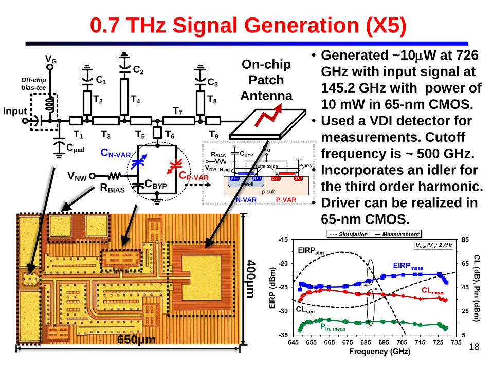
0.7 THz Signal Generation (X5)
• Generated ~10W at 726
GHz with input signal at
145.2 GHz with power of
10 mW in 65-nm CMOS.
• Used a VDI detector for
measurements. Cutoff
frequency is ~ 500 GHz.
• Incorporates an idler for
the third order harmonic.
• Driver can be realized in
65-nm CMOS.
18

Potential Applications
"Life was like a box of chocolates. You never know what you're gonna get."
You never know what you’re gonna get with life, but you may have more ideas
about what you’re gonna get in a box of chocolate.
Paper
Cup
Missing
Choco-
late
• Package inspection
• See through dry walls for detection
of studs, electrical wiring, and pipes.
• Authentication
• Medical imaging
• For a range of ~5 cm, -10 dBm TX and 20-dB NF receiver acceptable. 19
Corneal hydration
Z. Taylor et al, T-
TST2015

Far-IR Detection in CMOS up to 9.74THz
Freq.
(THz)
L x W
(μm2)
H
(μm)
Directivity
(dBi) hrad (%)
5 12 x 18 3.3 7.4 86
10 6.6 x 11 2.4 8.6 88
• Single cell 0.4 x 0.4 m2 Schottky diode
• Bypass capacitors are too inductive
• Biasing and signal extraction through the virtual ground at the mid
point of patch antenna.
• Direct connection without matching. Matching network has too much
loss (conduction and radiation).
• 130-nm UMC CMOS 20
RB
VB
Vsig
1-Cell
SBD
Patch
Antenna
RF Ground
IB
Resonant Length ~λ/2
|Z|I
V

21
• Diffusion region without implant forms a Silicide-Si junction.
• Ohmic contacts on n-well form the n-terminal.
• Schottky diode area is separated from ohmic contact by polysilicon gate on gate oxide layer.
• Single cell diode area is 0.4 x 0.4 m2 in 130-nm CMOS.
• Requires no process modifications.
• fcut-off over 2 THz in 130-nm CMOS.
02
1
CRf
total
cutoff
STI STIn+
ILD ILD
n-terminal Schottky terminal Ti/CoSi2-Si
Schottky Contact
n-well
n+
p-substrate
current
l1l2 ls l1 l2
Polysilicon
separator
ILDILD
STI STIn+
ILD ILD
n-terminal Schottky terminal Ti/CoSi2-Si
Schottky Contact
n-well
n+
p-substrate
current
l1l2 ls l1 l2
Polysilicon
separator
ILDILD
n+
implant l2
Poly ring width l1
n+ diffusion
ls
Polysilicon Gate Separated (PGS) Schottky Diodes
S. Sankaran et al., “Towards Terahertz Operation of CMOS,” 2009 ISSCC Feb. 2009.

Far-IR Detection in CMOS up to 9.74THz
22
10 THz 5 THz
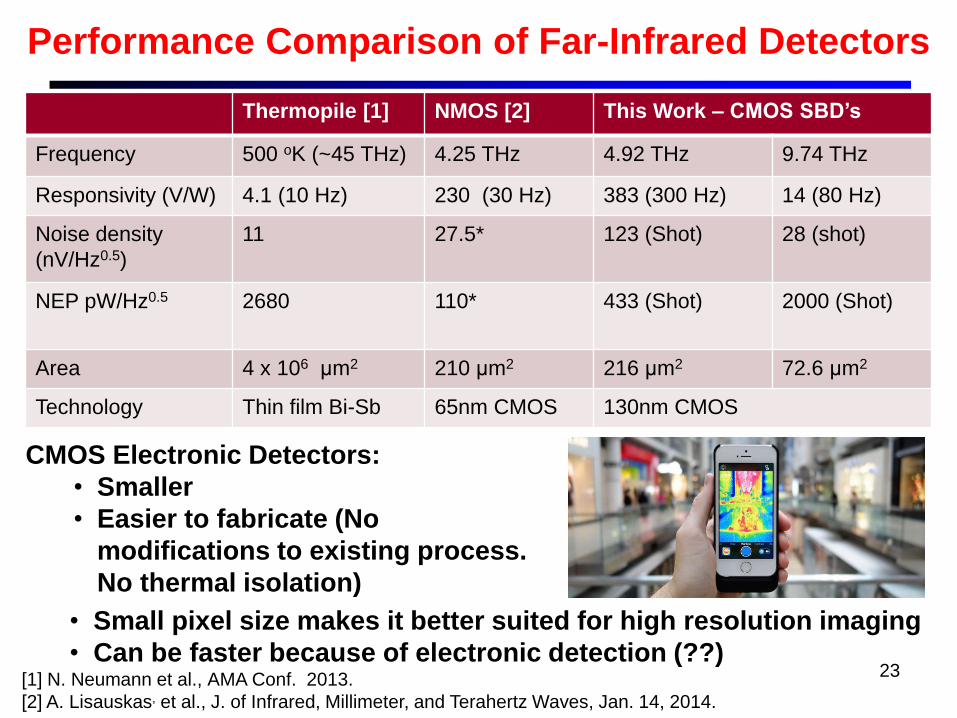
Performance Comparison of Far-Infrared Detectors
• Small pixel size makes it better suited for high resolution imaging
• Can be faster because of electronic detection (??) [1] N. Neumann et al., AMA Conf. 2013.
[2] A. Lisauskas, et al., J. of Infrared, Millimeter, and Terahertz Waves, Jan. 14, 2014.
CMOS Electronic Detectors:
• Smaller
• Easier to fabricate (No
modifications to existing process.
No thermal isolation)
23
Thermopile [1] NMOS [2] This Work – CMOS SBD’s
Frequency 500 oK (~45 THz) 4.25 THz 4.92 THz 9.74 THz
Responsivity (V/W) 4.1 (10 Hz) 230 (30 Hz) 383 (300 Hz) 14 (80 Hz)
Noise density
(nV/Hz0.5)
11 27.5* 123 (Shot) 28 (shot)
NEP pW/Hz0.5 2680 110* 433 (Shot) 2000 (Shot)
Area 4 x 106 μm2 210 μm2 216 μm2 72.6 μm2
Technology Thin film Bi-Sb 65nm CMOS 130nm CMOS

24
Outline
• Introduction
• CMOS Integrated Circuits and Systems
• Imaging
• Spectroscopy
• High data rate wireline communication
• Conclusions

25
180-300 GHz Spectrometer
Signal generator
180-300 GHz
Receiver
180-300 GHz Folded Absorption Cell, 30 cm
• Rotational spectroscopy.
• Does not need calibration for identification of molecules. Only depends
on spectra signature and independent of temperature.
• Specificity in the presence a large number type of molecules in a
mixture.
• Detect down to PPT for some gases.
F. Patten, MACS Proposer
Day Conf., Darpa, Nov. 2005

26
Some of Molecules on the EPA List
Gas Frequency
(MHz)
Fatality
Limit Gas
Frequency
(MHz)
Fatality
Limit
Hydrogen Cyanide
(HCN) 265887.1094
15-50
ppm/hr
Methyl Bromide
(CH3Br) 267801.2188
Cyanogen Chloride
(ClCN) 267199.53125
Ethylene Oxide
(C2H4O) 263292.5156
200
ppm/hr
Cyanogen Bromide
(BrCN) 263578.3438 Acrolein (C3H4O) 267279.3594
1.4
ppm/hr
Acetonitrile (CH3CN) 239096.6719 Propionitrile
(C2H5CN) 268829.0625
Carbonyl Sulfide
(OCS) 267530.4219
Vinyl Chloride
(C2H3Cl) 266151.2969
Methyl Chloride
(CH3Cl) 265785.4219
Methyl mercaptan
(CH3SH) 227564.6719
23
ppm/hr
Acrylonitrile
(C2H3CN) 265935.2031
Methyl isocyanate
(CH3NCO) 269788.6094 5 ppm/hr
Dichloromethane
(CH2Cl2) 259215.3906 Methanol (CH3OH) 250507.1563
Methyl Iodide (CH3I) 269864.9063 Formaldehyde 211211 100 ppb
Partial EPA list of Harmful Molecules

27
• Some 3000 different molecules have been detected.
• Breath analyses analyze blood, digestive system and environment.
• Spectrometer for blood sugar level detection for diabetic (Type I) patients (ethanol, acetone, methyl nitrate, ethyl benzene).
• Lung cancer detection.
• Current technique: gas chromatography mass spectrometry.
Blood Glucose Estimation from Breath

Breath Analyses Using Rotational Spectrometer
• Breathlyzer is confused by acetone. Diabetic patients have
acetone in their breath.
• Rotational spectrometer can distinguish acetone and ethanol.
• Acetone level has been correlated with the blood sugar level.
Ivan Medvedev, Wright State University. 28

Rotational Spectrometer for Breath Analyses
• Size of a desktop computer
• Costs ~ $100k in parts. ~$90k is for electronics
• Vacuum cell (10 mT)
• Needs a pre-concentration system to take out N2, O2, water ..
29

• Uses a fractional-N PLL with quadrature coupled oscillators to
generate 4 phases for X4 frequency to generate signals at 90-150
GHz.
• Amplification and frequency X2 to reach 180GHz to 300GHz
• Enables use of a single VCO to cover the entire frequency range.
• Output power of 1-20W
• FSK modulation
Transmitter Architecture
30

PFDLoop
Filter
Programmable
Divider
N=128 to 255
Charge
Pump
fref =150MHz
fqpll=85G-127GHzFSK
Modulation
Dummy Buffers
Q+ Q-
MC1 MC2
VDD
I+ I-
MC3 MC4
VDDWide-tuning
LC tanks
MCPL2 MCPL3MCPL1 MCPL4
C
RLOAD
Q+Q-I+ I-
LS1 LS2 LS3 LS4
1-1-1 MASH
Σ-Δ
Vout
Q+
Q-
I+I-
• Switched inductors and varactors for
coarse frequency tuning.
• Varactors for fine frequency tuning.
• FSK using S-D modulator of fractional
PLL
• Quadrature coupling to generate 4
switching events per oscillation period
at the output node.
Layout of the NMOS
switched differential
inductors
Differential Port
NMOS Switched
Differential Inductors
Center Tap
Vtune
3-bit Varactor
Bank
VC1-3
SW1
SW2
SW3
SW1
SW2
SW3
Center Tap
Differential Port
Schematic of the
wide-tuning
L-C tank
85-127 GHz Transmitter Prototype Design
31

Q+ Q-
MC1 MC2
VDD
I+ I-
MC3 MC4
VDDWide-tuning
LC tanks
MCPL2 MCPL3MCPL1 MCPL4
CC
RL (External, 50 )
Q+Q-I+ I-
LS1 LS2 LS3 LS4
Vout
Quadrature Oscillator
32
• Quadrature phase generation by passive coupling.
• No DC power consumption for the combining network.
• Improves phase noise.
• Eliminates the need for a broad band bias tee.
4f0
Wide-tuning LC VCO‘s coupled with a passive
quadrature coupling and phase combining network.
Difficult to implement.
Q+ Q- I+ I-
MCPL2 MCPL3MCPL1 MCPL4
CC
RL (External)
Q+Q-I+ I-
VDC
L Bias teeCpar
Combining
Node
Vout
J. Zhang, N. Sharma, W. Choi, D. Shim, Q. Zhong, and K. K. O, “85-to-127-GHz CMOS Signal Generation using a
Quadrature VCO with Passive Coupling and Broadband Harmonic Combining for Rotational Spectroscopy,” IEEE J. of
Solid State Circuits. Vol. 50, no. 6, pp. 1361-1371, June, 2015.

33
Fundamental-to-4th harmonic conversion
0 0.2 0.4 0.6 0.8 110
15
20
25
Phase Shift ()
Fundam
enta
l-to
-4th
Harm
onic
Pow
er
Conve
rsio
n L
oss
(dB
)
0 0.2 0.4 0.6 0.8 110
15
20
25
Phase Shift ()
Fundam
enta
l-to
-4th
Harm
onic
Pow
er
Conve
rsio
n L
oss
(dB
)Quadrature Mixing for Harmonic Generation
Q+ Q-
MC1 MC2
VDD
I+ I-
MC3 MC4
VDDWide-tuning
LC tanks
MCPL2 MCPL3MCPL1 MCPL4
CC
RL (External, 50 )
Q+Q-I+ I-
LS1 LS2 LS3 LS4
Vout

Coupling and Phase Combining Network
34
0 10 20 30 40 50 60 70 80
-16
-14
-12
-10
-8
-6
Ou
tpu
t P
ow
er (
dB
m)
LS (pH)
Band1
Band2
Band3
Band4
4.50 4.55 4.60-150
-75
0
75
150
Vo
ltag
e (m
V)
Time (ns)4.50 4.55 4.60
-20
-10
0
10
20
Cu
rren
t (m
A)
Time (ns)
0.00 0.25 0.50 0.75 1.00 1.25 1.50
-14
-12
-10
-8
-6
WCPL/WC
Ou
tpu
t P
ow
er (
dB
m)
92
94
96
98
100
Freq
uen
cy (GH
z)
Q+ Q-
MC1 MC2
VDD
I+ I-
MC3 MC4
VDDWide-tuning
LC tanks
MCPL2 MCPL3MCPL1 MCPL4
CC
RL (External, 50 )
Q+Q-I+ I-
LS1 LS2 LS3 LS4
Vout
• Degeneration inductors, LS1-LS4 for better power matching and enhanced
generation of 4th order harmonic.

PLL
modules
LC
Tank
1.3
mm
1.6mm
Divid
er
&
SD
Coupling capacitor
for 4xf0 output signalDummy VCO
Buffer
Inductive load for last
stage of VCO buffer
Three Stage
Buffer
Divider Coupling capacitor for
two phases of Divider
Cross
Coupled
transistors
for VCO
Coupling
transistors
NMOS
Switch
Coupling
node for 4xf0
output signal
Series
Inductor for
harmonic
boosting
NMOS
Switch
• Layout of 300 µm by 200 µm section around VCO.
• Harmonic combining transistors, inductors and other elements
arranged in a compact layout.
• Symmetry maintained around VCO using dummy buffers.
• Coupling node feeds the fourth harmonic signal to the output
transmission line.
• Fabricated in TI 65-nm CMOS.
Layout and Die Photograph
35

Phase Noise across frequency Power output across frequency
80 90 100 110 120 130-30
-25
-20
-15
-10
Band1
Band2
Band3 (high bias)
Band3
Band4 (high bias)
Ou
tpu
t P
ow
er (
dB
m)
Frequency (GHz)80 90 100 110 120 130
-110
-108
-106
-104
-102
-100
Band1
Band2
Band3 (high bias)
Band3
Band4 (high bias)
Ph
ase
No
ise
at 1
0MH
z o
ffse
t (d
Bc/
Hz)
Frequency (GHz)
• Phase noise meets the spectrometer requirement across the
frequency range (< -88 dBc/Hz at 10MHz offset @ 150 GHz).
• Output power is higher than -23 dBm across the whole range.
Phase Noise and Output Power
36
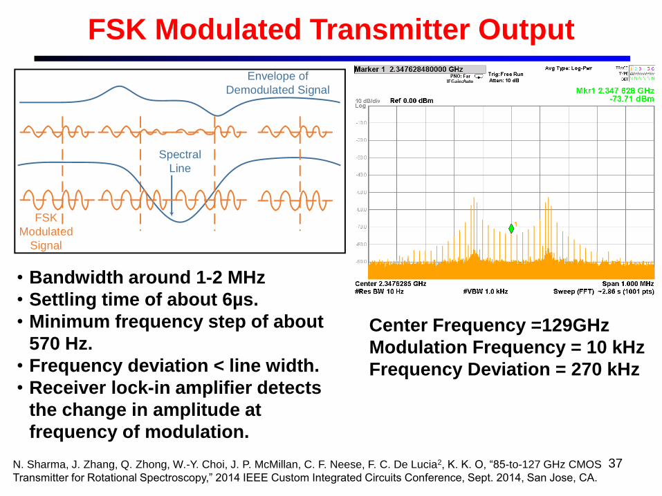
Spectral
Line
FSK
Modulated
Signal
Envelope of
Demodulated Signal
• Bandwidth around 1-2 MHz
• Settling time of about 6µs.
• Minimum frequency step of about
570 Hz.
• Frequency deviation < line width.
• Receiver lock-in amplifier detects
the change in amplitude at
frequency of modulation.
FSK Modulated Transmitter Output
Center Frequency =129GHz
Modulation Frequency = 10 kHz
Frequency Deviation = 270 kHz
37 N. Sharma, J. Zhang, Q. Zhong, W.-Y. Choi, J. P. McMillan, C. F. Neese, F. C. De Lucia2, K. K. O, “85-to-127 GHz CMOS
Transmitter for Rotational Spectroscopy,” 2014 IEEE Custom Integrated Circuits Conference, Sept. 2014, San Jose, CA.

Spectrometer Demonstration
38
Reference
Horn
Antenna
Bond wire
antenna and
PLL
Simulated Radiation Pattern
(Phi=90 degree @85GHz)
-23.00
-16.00
-9.00
-2.00
90
60
30
0
-30
-60
-90
-120
-150
-180
150
120
bondwireRadiation Pattern 1

Measured Gas Spectra
39

[6] [7] [8] [9] This Work
Architecture ADPLL FN Int. PLL PLL+ILVCO FN + Mult.
Process Tech. 65nm 90nm 65nm 65nm 65nm
fcenter (GHz) 60.5 40.4 74 61.7 106.7
Tuning Range 11.6% 6.2% 10.8% 11.9% 39.4%
Freq/Div Step /32 3kHz /8 2.16GHz ~570Hz
PN @ 10MHz -110 -114 -103 -113 -102 /-107
Fref Spur -74 -54 -49 -67/-58 -55/-70
Power (mW) 48 64 65 80 65/80
FOMT -170 -164 -162.9 -173.6 -178
• Tuning range is ~4X higher than all other millimeter wave PLLs while the
operating frequency is 30-60 GHz higher.
• Phase noise performance acceptable for rotational spectroscopy.
• Broadband amplifiers and frequency doubler are being implemented to
support 200-300 GHz operation.
Comparison Table
40

Dielectric Waveguide Communication
Noise Figure of Receiver: 20-dB Noise Figure for the 300-GHz 2nd harmonic mixer and 8-
dB Noise Figure for the 30-GHz bandwidth amplifier
Dielectric waveguide Launch Launch Demodulator
~
Modulated source
Frequency (THz) 0.18 to 0.36 Received power (dBm) -17.5
Channel Bandwidth (GHz) 45 Thermal noise density (dBm/Hz) -174
Range (m) 1 Noise figure of receiver (dB) 28
TX power to transition (dBm) -8 Bandwidth (bits/s (dB-Hz)) 30Gbps 105
Propagation loss 2.5 Eb/No (BER of 1x10-18) (dB) ~16
RX transition loss (dB) 3.5 Sensitivity (dBm) -25.0
TX transition loss (dB) 3.5 Link margin (dB) ~7.5
• Channelizing ~200GHz bandwidth using frequency and polarization
division multiple access, perhaps enable ~300 Gbps communication.
• Given ~-3 dBm at 447 GHz, TX power can be increased to improve the
link margin.
• No photonic components needed. Maybe able to compete with photonics
on the chip-to-chip and board-to-board communications. 41

94 95 96 97 98 99 00 01 02 03 04 05 06 07 08 09 10 11 12 13 14 15 16
900 MHz CMOS LNA, 1996
4 GHz, CMOS LNA,
13GHz Amp. In SOI
CMOS, 1998
25.9 GHz, CMOS
VCO, 2000
f0
2f0
VCO ILFD
÷51
2
PFD &
Charge
Pump
Loop
Filter
fREF
Phase Locked
100 GHz, 2007
10-THz Detector,
2014
Doubling operating
frequency every 18 months
10 THz
1 THz
100 GHz
10 GHz
1 GHz
Patch
Antenna
VDD
4-Push Oscillator
GND GNDVB
540 µm
530 µ
m
553-GHz Signal
Generator, 2011
• Imaging, spectroscopy and broadband wireline
communications are exciting potential applications
that can revolutionize communications and medicine.
• Sub-millimeter wave systems in CMOS are possible.
• Detection up to 10THz has been demonstrated.
• Generation of 1mW in CMOS at 1THz should be
possible.
• Should be a path to 40-THz detection for Infrared
imaging. 192-GHz Signal
Generation and
Detection, 2006
IN
GND GND
GND
GND
GND VampVCVdiodeVctrlVoscVBufferVbias
SV
OUT
FVGND
410-GHz Signal
Generation, 2008
Pa
tch
An
ten
na
Pu
sh-p
ush
VC
O
GN
DG
ND
VD
DV
DD
V1
860-GHz
Detector, 2012

43
Acknowledgement
• The efforts were supported by
• DARPA (N66001-03-1-8901)
• NASA (NAG10-316)
• SRC (Task ID: 1327, 1386).
• SRC TxACE (Task ID: 109, 152)
• C2S2 (Task ID: 2047.004.004, 2047.004.011)
• Samsung Electronics (GRO)
• The authors also thank TI for fabrication support.