cmos-compatible high-speed silicon photodetectors …tera.yonsei.ac.kr/publication/pdf/phd_2009_...
TRANSCRIPT

CMOS-Compatible High-Speed
Silicon Photodetectors for Gbps Fiber-Fed
Wireline/Wireless Communication Systems
Hyo-Soon Kang
THE GRADUATE SCHOOL
YONSEI UNIVERSITY
Department of Electrical and Electronic Engineering

CMOS-Compatible High-Speed
Silicon Photodetectors for Gbps Fiber-Fed
Wireline/Wireless Communication Systems
A Dissertation
Submitted to the Department of Electrical and Electronic Engineering
and the Graduate School of Yonsei University
in partial fulfillment of the requirements for the degree of
Doctor of Philosophy
Hyo-Soon Kang
January 2009

ii
This certifies that the dissertation of Hyo-Soon Kang is approved.
___________________________ Thesis Supervisor: Woo-Young Choi
___________________________ Sang-Kook Han
___________________________
Ilgu Yun
___________________________
Jinwook Burm
___________________________
Hyuk-Kee Sung
The Graduate School
Yonsei University
January 2009

Table of Contents
Abstract ............................................................................................... xii
1. Introduction .................................................................................... 1
1-1. Recent trends of optical communication systems ................... 1
1-2. CMOS-compatible optical receivers ....................................... 3
1-3. Outline of dissertation ............................................................. 7
2. Design of CMOS-Compatible Silicon Avalanche Photodetectors
10
2-1. Design considerations for CMOS-APDs ............................... 10
2-2. TCAD simulation .................................................................. 17
2-2-1. Two PN-junctions in CMOS technology: P+/N-Well and N-Well/P-Substrate junctions ......................................... 17
2-2-2. Influence of the P+ region width on bandwidth ......... 21
2-2-3. Electric field profile with and without STI ................ 23
2-3. Structure of the fabricated CMOS-APD ................................ 25
3. Characterization of the fabricated CMOS-APDs ..................... 27
3-1. Experimental setup for characterization of CMOS-APDs .... 27
3-2. DC characteristics .................................................................. 29
3-3. Photodetection frequency responses ...................................... 36
3-4. Equivalent circuit modeling .................................................. 40
3-4-1. Impedance characteristics of the CMOS-APD .......... 40
3-4-2. Equivalent circuit model for the CMOS-APD ........... 44
3-4-3. Parameter extraction ................................................... 47
4. 6.25-Gbps wireline data transmission using the CMOS-APD . 53
4-1. Optical receiver using the CMOS-APD ................................ 53
4-2. Experimental setup for 6.25-Gbps data transmission ............ 56
4-3. Data transmission results ....................................................... 57
iii

5. Utilization of CMOS-APDs for fiber-fed 60-GHz self-
heterodyne wireless systems ............................................................... 60
5-1. Fiber-fed 60-GHz self-heterodyne wireless systems ............. 60
5-2. Optoelectronic mixer ............................................................. 64
5-2-1. System configuration using a 60-GHz harmonic optoelectronic mixer based on the CMOS-APD ................... 64
5-2-2. Operation principle and characteristics of the CMOS-compatible harmonic optoelectronic mixer (CMOS-HOEM) using the CMOS-APD .......................................................... 67
5-2-3. Experimental setup for downlink data transmission .. 72
5-2-4. Demonstration of data transmission through the fiber-fed 60-GHz self-heterodyne system using the CMOS-HOEM .............................................................................................. 74
5-3. Self-oscillating optoelectronic mixer .................................... 76
5-3-1. System configuration using a 60-GHz self-oscillating harmonic optoelectronic mixer based on the CMOS-APD .. 76
5-3-2. Configuration and characteristics of the CMOS-compatible self-oscillating harmonic optoelectronic mixer (CMOS-SOHOM) ................................................................. 78
5-3-3. Experimental setup for downlink data transmission .. 85
5-3-4. Demonstration of data transmission through the 60-GHz self-heterodyne wireless system using the CMOS-SOHOM ................................................................................ 87
6. Implementation of low-cost Radio-over-Fiber systems using
CMOS-APDs ....................................................................................... 92
6-1. Introduction ........................................................................... 92
6-2. RoF transmission of cellular or WLAN signal ...................... 96
6-2-1. Experimental setup for RoF transmission of WCDMA or WLAN signal .................................................................... 96
6-2-2. RoF transmission of WCDMA signal ...................... 100
6-2-3. RoF transmission of IEEE 802.11a WLAN signal ... 104
iv

6-3. Low-cost RoF downlinks for multi-standard signal transmission ................................................................................ 108
6-3-1. Experimental setup for RoF transmission of both WCDMA and IEEE 802.11g WLAN signals ...................... 108
6-3-2. Demonstration of multi-standard signals transmission ............................................................................................ 111
7. Summary .................................................................................... 114
References .......................................................................................... 117
List of Publications ........................................................................... 124
v

List of Figures and Tables Fig. 1-1. Applications of short-distance optical communication systems:
(a) optical access networks and (b) optical interconnects [1]. ........ 2
Fig. 1-2. Block diagram of an integrated CMOS optical receiver, which consists of a CMOS-compatible photodetector (CMOS-PD) and electronic circuits including a transimpedance amplifier (TIA), a limiting amplifier (LA), an equalizer (EQ), and clock-and-data recovery (CDR) circuits. ................................................................. 6
Fig. 1-3. Simplified cross sectional device structures of CMOS technology. ...................................................................................... 6
Fig. 2-1. PN-junctions formed by P+/N-Well and N-Well/P-substrate
regions in standard CMOS technology. The values in parentheses shows estimated doping concentrations. Dashed lines indicate depletion regions formed in PN-junctions. ................................... 12
Fig. 2-2. Cross-sectional structure of a CMOS-compatible avalanche photodetector for TCAD simulation. ............................................ 19
Fig. 2-3. Simulated photodetection frequency responses extracted at P+ contact and N-Well contact: (a) current density and (b) normalized frequency responses. ..................................................................... 20
Fig. 2-4. Simulated photodetection frequency response with different P+ region widths of 2 μm, 3 μm, and 6 μm: (a) device structure for simulation and (b) normalized frequency responses. .................... 22
Fig. 2-5. Electric field profiles of P+/N-Well junctions in the CMOS-APD (a) without STI and (b) with STI. (STI: shallow trench isolation) ....................................................................................... 24
Fig. 2-6. (a) Cross-sectional structure of the fabricated CMOS-APD. (b) Simplified layout. .................................................................... 26
vi

Fig. 3-1. Experimental setup for CMOS-APD characterization: (a) DC, photodetection frequency response, and (b) reflection coefficients measurement. ................................................................................ 28
Fig. 3-2. Current-voltage characteristics of the fabricated CMOS-APD under dark and illumination. Incident optical power (Popt) is 0.1 mW. ............................................................................................... 31
Fig. 3-3. Responsivity and avalanche multiplication factor (M) as a function of the reverse bias voltage (VR) under 0.1 mW optical illumination. .................................................................................. 32
Fig. 3-4. Avalanche multiplication factors as a function of incident optical power at VR of 10.0 and 10.2 V. ........................................ 34
Fig. 3-5. Current-voltage characteristics of the fabricated CMOS-APD at different temperatures under dark condition. The temperature increases from room temperature (about 25 °C) to 175 °C with 25 °C increments. .......................................................................... 35
Fig. 3-6. (a) Photodetection frequency responses at different VR when incident optical power is 0.2 mW. (b) Enlarged current-voltage characteristics near VBK,dark to clearly show measurement condition. ...................................................................................... 37
Fig. 3-7. Photodetection frequency responses of the CMOS-APD with different optical powers at (a) VR of 10.2 V and (b) VR of 10.3 V. Incident optical power increases from 0.2 mW to 1.0 mW with 0.4 mW increments. Insets show relative responses without normalization. ............................................................................... 38
Fig. 3-8. IMPATT diode model for describing the avalanche region, drift region, and inactive region of PN-junction diodes. .............. 43
Fig. 3-9. Reflection coefficients of the CMOS-APD at the output port (P+ contact) with different bias voltages when 0.5 mW optical signal is injected. The inset table shows measured current values. ...................................................................................................... 43
Fig. 3-10. Equivalent circuit model for the CMOS-APD. .................... 46
Fig. 3-11. Measured and fitted reflection coefficient at the P+ port
vii

under 1 mW optical illumination. Hollow circles show measured data and solid lines represent fitted results using the model. ........ 51
Fig. 3-12. (a) Measured photodetection frequency responses and simulation results with the model at different bias currents. (b) The rf peaking effect and the transit-time effect on the photodetection frequency response. ...................................................................... 52
Fig. 4-1. (a) A schematic of optical receiver having the CMOS-APD
and the transimpedance amplifier on a board. (b) A photograph of the fabricated CMOS-APD receiver. ............................................ 54
Fig. 4-2. Photodetection frequency responses of the CMOS-APD and optical receiver. ............................................................................. 55
Fig. 4-3. Experimental setup for 6.25-Gbps data transmission using the optical receiver based on the CMOS-APD. .................................. 56
Fig. 4-4. 6.25-Gbps data transmission results: (a) BER characteristics as a function of incident optical power and (b) eye diagram at Popt = -2 dBm. ...................................................................................... 58
Fig. 5-1. Downlink configurations of remote up-conversion systems:
(a) a conventional fiber-fed 60-GHz super-heterodyne systems and (b) a fiber-fed 60-GHz self-heterodyne systems. .......................... 63
Fig. 5-2. The downlink configuration of fiber-fed 60-GHz self-heterodyne wireless systems using a CMOS-compatible harmonic optoelectronic mixer (CMOS-HOEM) based on the CMOS-APD. ...................................................................................................... 66
Fig. 5-3. Schematic diagram of harmonic optoelectronic mixing utilizing the CMOS-APD and the spectrum of frequency up-converted signals when 30 GHz electrical LO and 100 MHz optical IF signals are applied to the device. .................................. 68
Fig. 5-4. Frequency up-converted signal powers (USB at 60.1 GHz and LSB at 59.9 GHz) as well as photodetected IF signal powers at 100 MHz as functions of the reverse bias voltage applied to the
viii
CMOS-HOEM. ............................................................................. 70
Fig. 5-5. Frequency up-converted signal powers (USB and LSB) and second harmonic LO signal powers as functions of electrical LO signal power injected to the CMOS-HOEM. ................................ 71
Fig. 5-6. Experimental setup for downlink data transmission through the fiber-fed 60-GHz self-heterodyne system using the CMOS-compatible harmonic optoelectronic mixer (CMOS-HOEM). ..... 73
Fig. 5-7. (a) Frequency down-converted signal spectrum at the output of Schottky diode envelop detector. (b) Constellation and eye diagram of demodulated 25-Mbps 32-QAM data at the vector signal analyzer. .............................................................................. 75
Fig. 5-8. Downlink configuration of the fiber-fed 60-GHz self-heterodyne wireless system using the CMOS-compatible self-oscillating harmonic optoelectronic mixer (CMOS-SOHOM) based on the CMOS-APD ............................................................. 77
Fig. 5-9. (a) Schematic diagram of the CMOS-SOHOM having the CMOS-APD and the 30-GHz feedback loop. (b) Spectrum of second harmonic self-oscillating signal of the CMOS-SOHOM. . 79
Fig. 5-10. Output spectrum of the CMOS-SOHOM when 950 MHz optical IF signal is injected to the device. ..................................... 80
Fig. 5-11. Photodetected IF signal powers at 950 MHz as functions of the reverse bias voltage with and without self-oscillation by turning on/off the amplifier in the feedback loop. ........................ 83
Fig. 5-12. Frequency up-converted signal power (LSB at 2·fLO – fIF) and photodetected IF signal power (fIF) as functions of the reverse bias voltage of the CMOS-SOHOM. ................................................... 84
Fig. 5-13. Experimental setup for downlink data transmission through the fiber-fed 60-GHz self-heterodyne wireless system based on the CMOS-compatible self-oscillating harmonic optoelectronic mixer (CMOS-SOHOM). ........................................................................ 86
Fig. 5-14. Spectrum of frequency down-converted 25-Mbps 32-QAM data to IF band at the mobile terminal. ......................................... 89
ix

Fig. 5-15. (a) Constellation and (b) eye diagram of demodulated data at the vector signal analyzer. ............................................................. 90
Fig. 5-16. RMS error vector magnitude (EVM) and signal-to-noise ratio (SNR) measured at the output of Schottky diode envelop detector in the mobile terminal as a function of incident optical power into the CMOS-SOHOM at the base station. ....................................... 91
Fig. 6-1. Applications of Radio-over-Fiber (RoF) systems for cellular
and/or WLAN signal distribution. ................................................ 95
Fig. 6-2. Schematic diagram of low-cost Radio-over-Fiber downlink systems using CMOS-compatible photodetectors. ....................... 95
Fig. 6-3. Experimental setup for RoF downlink data transmission of WCDMA or WLAN signal. .......................................................... 98
Fig. 6-4. Photodetection frequency response of the CMOS-APD receiver used in the experiments. WCDMA and IEEE 802.11a signal bands are designated. .......................................................... 99
Fig. 6-5. Dependence of error vector magnitude for demodulated WCDMA signal (a) on input RF power to the electro-optic modulator and (b) on input optical power to the CMOS-APD receiver at the base station. ......................................................... 102
Fig. 6-6. Spectrum of WCDMA signal at the output of the CMOS-APD receiver in the base station. ......................................................... 103
Fig. 6-7. Constellation of demodulated WCDMA signal at the vector signal analyzer in the mobile terminal. EVM of 3.26 % is obtained. ...................................................................................... 103
Fig. 6-8. Dependence of error vector magnitude for demodulated WLAN signal (a) on input RF power to the electro-optic modulator and (b) on input optical power to the CMOS-APD receiver at the base station. ......................................................... 106
Fig. 6-9. Spectrum of IEEE 802.11a WLAN signal at the output of the CMOS-APD receiver in the base station. ................................... 107
Fig. 6-10. Constellation of demodulated WLAN signal at the vector
x

signal analyzer in the mobile terminal. EVM of 2.89 % is obtained. ...................................................................................... 107
Fig. 6-11. Experimental setup for low-cost RoF downlink to transmit multi-standard signals of WCDMA and IEEE 802.11g WLAN. 110
Fig. 6-12. Measured frequency response of 300-m long multimode fiber (MMF). ....................................................................................... 110
Fig. 6-13. (a) Spectrum of RoF transmitted multi-standard signals at the output of the CMOS-APD receiver. Enlarged spectrums of (b) WCDMA and (c) IEEE 802.11g WLAN signals. ....................... 112
Fig. 6-14. EVM results of RoF transmission of multi-standard signals. (a) EVM of demodulated WCDMA signal as a function of WLAN signal power. (b) EVM of demodulated WLAN signal as a function of WCDMA signal power. ............................................ 113
Table 3-1. Extracted circuit parameters of ZP+/N-Well. ............................ 49
Table 3-2. Extracted parasitic components. .......................................... 49
Table 4-1. Performance comparison of optical receivers based on
CMOS-compatible photodetectors. .............................................. 59
xi

Abstract
Silicon avalanche photodetectors are designed and fabricated with
standard CMOS technology. By conducting technology computer-
aided-design (TCAD) simulation for optimum device structures in
standard CMOS technology, CMOS-compatible avalanche
photodetectors (CMOS-APDs) having high gain and large bandwidth
are implemented.
From the measurements of DC and photodetection frequency
response characteristics, the performance of the fabricated CMOS-
APDs is experimentally investigated. When the CMOS-APD operates
in an avalanche regime by applying high reverse bias voltage to the
device, rf peaking in photodetection response is observed. To clarify the
physical origin of the rf peaking effect, impedance characteristics are
investigated, and an inductive component in an avalanche region is
modeled. Through the equivalent circuit modeling of the CMOS-APD,
all the circuit parameters including the avalanche inductance, the
junction capacitance, the parasitic components, and the transit-time
constants for photogenerated carriers are extracted.
To demonstrate high-speed optical signal transmission, CMOS-APD
receivers having a CMOS-APD and a transimpedance amplifier are
xii

fabricated on a board. Using the CMOS-APD receiver, error-free data
transmission at the data rate of 6.25 Gbps is successfully performed
with bit error rate (BER) less than 10-12.
For realization of cost-effective fiber-fed 60-GHz self-heterodyne
wireless systems, CMOS-APDs are utilized as a CMOS-compatible
harmonic optoelectronic mixer (CMOS-HOEM) to simultaneously
perform photodetection and frequency up-conversion to 60-GHz band.
The optoelectronic mixing is performed with the help of the nonlinear
characteristics of avalanche multiplication factor. Furthermore, a
CMOS-compatible self-oscillating harmonic optoelectronic mixer
(CMOS-SOHOM) is implemented by connecting a CMOS-APD and a
30-GHz band electrical feedback loop. Using these CMOS-HOEM and
CMOS-SOHOM, 25-Mbps 32-QAM data are transmitted through fiber-
fed 60-GHz self-heterodyne wireless downlinks.
Finally, for implementation of cost-effective radio-over-fiber (RoF)
systems, CMOS-APD receivers are adopted in base stations for RoF
receivers. Single standard signal of 2.1-GHz WCDMA or 5.2-GHz
IEEE 802.11a is RoF transmitted using a CMOS-APD receiver. In
addition, low-cost RoF systems consisting of an 850-nm vertical-cavity
surface-emitting laser (VCSEL), 300-m multimode fiber, and a CMOS-
APD receiver are realized to transmit multi-standard RoF signals of
xiii

xiv
2.1-GHz WCDMA and 2.4-GHz IEEE 802.11g WLAN, simultaneously.
Keywords: Avalanche photodetector, Avalanche photodiode, Avalanche inductance, CMOS technology, Fiber-fed wireless system, Optoelectronic mixer, Radio-over-fiber system, Self-heterodyne system, Self-oscillating optoelectronic mixer

1. Introduction 1-1. Recent trends of optical communication systems
Rapidly growing demand for high-capacity data transmission has
accelerated the evolution of optical communication systems from long-
haul backbone infrastructures to short-distance optical networks to
enhance the penetration of fiber further toward end-users. Moreover,
large variety of electrical interconnects including board-to-board and
chip-to-chip connections are to be replaced by optical interconnects due
to such advantages of optical technology as huge bandwidth, light
weight of transmission medium, and immunity to electrical
interferences [1-3]. Fig. 1-1 shows emerging applications of optical
communication systems such as short-distance optical access networks
and optical interconnects.
With these trends of optical communications, several standards
including Gigabit Ethernet (GbE), fiber channel [4], and fiber channel
over Ethernet (FCoE) [5] are established or recently pursued. However,
for successful realization of these optical communication systems, large
amount of optical transceivers and wide deployment of optical
transmission medium are indispensable. Consequently, cost-effective
realization of optical components as well as optical transmission
1

medium is the most critical issue.
For optical transmitters, AlGaAs/GaAs vertical-cavity surface-
emitting lasers (VCSELs) operating at 850 nm are promising
candidates due to their low fabrication cost [6], [7]. Together with low-
cost VCSELs, multimode fibers have been regarded as cost-effective
solutions for transmission medium owing to its easy installation.
However, as of yet, optical receivers are challenging parts for the
implementation in a cost-effective manner.
Network
Board-to-Board
Chip-to-chip
Intra-chip• 10 GbE• Fiber Channel
ISP
(IEEE spectrum, 2002)
• FTTH
Campus
Data center
Opticalfiber
(a) Optical Access Networks (b) Optical Interconnects
Fig. 1-1. Applications of short-distance optical communication systems: (a) optical access networks and (b) optical interconnects [1].
2

1-2. CMOS-compatible optical receivers
Complementary metal-oxide-semiconductor (CMOS) technology
can provide a powerful solution for low-cost realization of optical
receivers [8]. For the past decades, CMOS technology has been used
for all types of electronic circuits including analog, digital, and RF
applications with the help of its high-volume manufacturability, low
fabrication cost, and technological advances. Furthermore, silicon
photodetectors fabricated with standard CMOS technology can detect
850-nm optical signals which are widely used for short-distance optical
communication systems. Recently, it has been also reported that
CMOS-based photodetector can be utilized for 1300/1550-nm optical
communication system by adopting germanium layer on silicon
substrate with some process modifications [9]. Consequently, well
developed CMOS technology can enable cost-effective integrated
optical receivers having a photodetector and required electronic circuits
such as a transimpedance amplifier (TIA), a limiting amplifier (LA), an
equalizer (EQ), and clock-and-data recovery (CDR) circuits on a single
chip as shown Fig. 1-2.
In spite of these advantages, there are inherent drawbacks of CMOS
technology for photodetector applications. Fig. 1-3 shows simplified
cross sectional device structures of CMOS technology. NMOSFET and
3

PMOSFET are formed by N+ and P+ source/drain regions on P-Well
and N-Well, respectively, with gate oxides and poly-silicon gates. In
this structure, two PN-junctions for photodetectors can be realized with
P+ to N-Well and N-Well to P-Substrate junctions [10]. However, large
optical penetration depth of 14 μm in silicon at the wavelength of 850
nm makes it difficult to achieve high responsivity because depletion
regions of PN-junctions are usually formed in less than 1 μm under the
silicon surface [11]. The responsivity is defined as the ratio of the
photocurrent to incident optical power. Moreover, the shallow depletion
region due to relatively high doping concentrations in N-Well and P-
Substrate causes diffusive transport of the photogenerated carriers in
the charge neutral region, limiting high-speed operation.
To improve responsivity and bandwidth of CMOS photodetectors,
several approaches have been carried out. A low-doped epitaxial layer
in the twin-well process was used to enhance the depletion width and
quantum efficiency, resulting in an 1-Gbps optical receiver with 44 %
quantum efficiency [12]. In addition, a lateral p-i-n photodetector based
on silicon-on-insulator (SOI) substrate, in which slow diffusion
currents in the substrate region are blocked, achieved 10-Gbps
operation [13]. Although the performance of above CMOS
photodetectors is impressive, their realization requires additional
4

fabrication costs and an approach based on the standard CMOS
technology is desired in order to fully utilize the cost advantage of
CMOS photodetectors.
With the standard CMOS process, spatially modulated light (SML)
detectors in which differential signaling was used to subtracting the
slow diffusion tail, resulting in 2-Gbps optical receiver [8]. However, it
has weakness of relatively low responsivity and speed limitation due to
current subtraction and large active area, respectively. By using
equalizer circuits to compensate low-speed photodetectors, a 3-Gbps
optical receiver was developed [14]. This scheme, though, requires
knowledge in accurate photodetector responses and complicates the
receiver circuit design. Recently, p+-p-n avalanche structure has been
reported that provides high speed and high responsivity [15]. Based on
this photodetector, bandwidth enhancement technique by eliminating
slow diffusion photogenerated carriers was also devised [16]. Although
this structure provides high responsivity owing to a large depletion
region formed by N-Well/P-Substrate junction, relatively high dark
current can be generated. Furthermore, the advantage of high
responsivity can be sacrificed by body voltages applied for elimination
of slow diffusion components. More severely, positive body voltages
make it difficult to implement integrated optical receivers because the
5

substrate potential of all the electronic circuits should be set to ground.
In this dissertation, CMOS-compatible avalanche photodetectors
(CMOS-APDs) having high responsivity and large bandwidth are
presented for low-cost optical communication systems.
VCSEL CMOS-PD
TIAMultimode
Fiber
(λ = 850nm)
Integrated CMOS Optical Receiver
EQ CDR
LA
Fig. 1-2. Block diagram of an integrated CMOS optical receiver, which consists of a CMOS-compatible photodetector (CMOS-PD) and electronic circuits including a transimpedance amplifier (TIA), a limiting amplifier (LA), an equalizer (EQ), and clock-and-data recovery (CDR) circuits.
NMOSFET PMOSFET PN-junctions
Fig. 1-3. Simplified cross sectional device structures of CMOS technology.
6

1-3. Outline of dissertation
This dissertation will focus on CMOS-compatible avalanche
photodetectors (CMOS-APDs) and their applications for Gbps
baseband data transmission, fiber-fed 60-GHz self-heterodyne wireless
system, and low-cost radio-over-fiber systems. Design consideration
and characteristics of fabricated CMOS-APDs also will be presented.
Details of dissertation outline are as follows.
In chapter 2, design considerations for CMOS-APDs to achieve
high responsivity and high speed are introduced at first. Section 2-2
shows simulation results of technology computer-aided-design (TCAD)
for the optimization of CMOS-APDs. The structure of fabricated
CMOS-APDs is explained in section 2-3.
Chapter 3 shows characteristics of the fabricated CMOS-APD.
Experimental setup for device characterization is explained in section
3-1. Characteristics of DC and photodetection frequency response are
followed in section 3-2 and 3-3, respectively. Section 3-4 presents an
equivalent circuit model and extracted parameters from the
measurement of RF impedances and photodetection frequency
responses.
In chapter 4, 6.25-Gbps baseband data transmission is demonstrated.
Section 4-1 describes a CMOS-APD receiver, which is implemented
7

with a CMOS-APD and a transimpedance amplifier (TIA) on a board.
Experimental setup is described in section 4-2 and 6.25-Gbps data
transmission results are shown in section 4-3.
For applications of fiber-fed 60-GHz self-heterodyne wireless
systems, CMOS-APDs are utilized for a harmonic optoelectronic mixer
(CMOS-HOEM) and a self-oscillating harmonic optoelectronic mixer
(CMOS-SOHOM). The architecture and characteristics of self-
heterodyne wireless systems are introduced in section 5-1. Operation
principle of harmonic frequency up-conversion by utilizing a CMOS-
APD as a harmonic optoelectronic mixer is explained in section 5-2.
Experiments of frequency up-conversion to 60-GHz band and 25-Mbps
32-QAM data transmission are also demonstrated. Section 5-3 shows
the results of the self-oscillating harmonic optoelectronic mixer using a
CMOS-APD. Configuration and performance of the self-oscillating
mixer are presented. Demonstration of 25-Mbps 32-QAM data
transmission is also presented in section 5-3.
In chapter 6, cost-effective Radio-over-Fiber (RoF) systems using
the CMOS-APDs are presented. Section 6-2 demonstrates single
standard RoF transmission for 2.1-GHz WCDMA or 5.2-GHz 802.11a
WLAN using the CMOS-APD receiver. With the CMOS-APD receiver
as well as a VCSEL, both 2.1-GHz WCDMA and 2.4-GHz 802.11g
8

WLAN signals are simultaneously transmitted via 300-m multimode
fiber and the experimental results are presented in section 6-3.
Finally, the dissertation will be summarized in chapter 7.
9

2. Design of CMOS-Compatible Silicon Avalanche
Photodetectors 2-1. Design considerations for CMOS-APDs
When optical signals in which photon energy is larger than bandgap
energy of semiconductor are illuminated to photodetectors, incident
photons generate electron-hole pairs in semiconductor regions. Among
these generated carriers, carriers in the depletion regions can only
induce currents to external circuits because the electric field in the
depletion region causes drift of carriers. With these drift currents, some
amounts of photogenerated carriers in the charge neutral region can
enter into the depletion regions with diffusive transport thus generate
photocurrents. Consequently, the depletion width of PN-junction
dominantly affects the performance of photodetectors.
Using standard CMOS technology, PN-junctions can be
implemented. Fig. 2-1 shows simplified cross-sectional structure of
PN-junctions in standard CMOS technology. There are two PN-
junctions which are formed by P+ source/drain to N-well regions and
N-well to P-substrate regions. The depletion width (W) built in PN-
junctions can be estimated by following equations with the assumption
of abrupt PN-junctions [17].
10

2lnB Abi
i
k T N NVq n
⎛ ⎞= ⎜ ⎟
⎝ ⎠D [V] (2.1)
( )2 s A Dbi R
A D
N NW Vq N Nε ⎛ ⎞+
= +⎜ ⎟⎝ ⎠
V [m] (2.2)
where, Vbi is built-in voltage of a PN-junction, kB is Boltzmann constant,
T is temperature, q is electron charge, NA is acceptor doping
concentration, ND is donor doping concentration, ni is intrinsic carrier
concentration of silicon, εs is permittivity of silicon, and VR is the
reverse bias voltage.
11

Fig. 2-1. PN-junctions formed by P+/N-Well and N-Well/P-substrate regions in standard CMOS technology. The values in parentheses shows estimated doping concentrations. Dashed lines indicate depletion regions formed in PN-junctions.
12

From (2.2), the depletion widths of P+/N-Well and N-Well/P-
Substrate junctions under zero-bias condition are calculated as 0.09 μm
and 0.98 μm, respectively. Due to the low doping concentration of the
P-Substrate region compared with the P+ source/drain region, large
depletion width by the N-Well/P-Substrate junction can be formed. For
efficient collection of the photogenerated carriers, therefore, the N-
Well/P-Substrate junction is more suitable than the P+/N-Well junction.
Although the N-Well/P-Substrate junction can generate larger
photocurrents, carrier transport mechanism, which determines speed of
photodetectors, should be considered as well.
The speed of PN-junction photodetectors is mainly limited by three
time constants: carrier drift time in the depletion region (τdrift), carrier
diffusion time in the charge neutral region (τdiffusion), and RC time
constant (τRC) as explained in following equations [18].
20
/
/ (2 )
( )
drift
diffusion
RC S L
W v
l D
R R CJ
τ
τ
τ
=
= ⋅
= + ⋅ (2.3)
where, W is the depletion width, v is carrier velocity under the applied
electric field, l0 is diffusion length of the charge neutral region, D is
13

diffusion constant of silicon, RS is series resistance, RL is load
resistance, and CJ is junction capacitance formed in a PN-junction.
As mentioned before, photocurrents are induced by the
photogenerated carriers in the depletion region as well as the diffusive
carriers entered into the depletion region from the charge neutral
regions. Since depletion widths of PN-junctions are relatively narrow
compared with the length of the charge neutral region in standard
CMOS technology, large amounts of optical signals are absorbed in the
charge neutral region and the speed of PN-junction photodetectors are
dominantly constrained by the diffusion time. Especially for N-Well/P-
Substrate junction, large diffusion currents can be generated in the P-
Substrate region and these severely limit the photodetector speed.
Accordingly, the P+/N-Well junction is favorable for the high-speed
photodetector in spite of its low photocurrents due to the narrow
depletion width. Furthermore, optimized device layout for reducing the
series resistance and the junction capacitance, which are dependent on
area of the active region, is required for diminishing RC-time limit.
Although the above mentioned considerations are taken into
account for design of photodetectors, the performance of CMOS-PDs is
still insufficient for high-speed optical communication systems. For
instance, the P+/N-Well junction photodetector has diffusion time
14

constant of approximately 0.23 ns, which corresponds to 3-dB
bandwidth of about 0.69 GHz at the reverse bias voltage of 5 V. For this
estimation, the depletion width of 0.23 μm is calculated from the P+/N-
Well junction and diffusion coefficient of 7.8 cm2/s is assumed at
doping concentration of 1.5 ⅹ 1017 cm-3 in the N-Well region. The
narrow depletion width, which is much smaller than the 850-nm optical
penetration depth of 14 μm in silicon, is also problematic for absorption
efficiency.
To solve these intrinsic problems of low responsivity and limited
speed, this dissertation concentrates on the implementation of
avalanche photodetectors using standard CMOS technology. With the
help of avalanche multiplication process, the photogenerated carriers
can be amplified thus photocurrent increased. Furthermore, bandwidth
of photodetectors can be enhanced by the enlarged depletion width
under high electric field owing to reduced diffusive carriers and
shortened diffusion length. In this dissertation, the rf peaking effect in
photodetection frequency response is also presented with equivalent
circuit modeling. The avalanche inductance appeared in the avalanche
region can induce rf peaking and this results in bandwidth enhancement
of avalanche photodetectors.
To realize avalanche photodetectors using standard CMOS
15

technology, an additional factor should be considered for device
optimization. When the electric field increases with the increasing
reverse bias voltage, avalanche multiplication process starts to occur
more likely in the lateral junction periphery due to the stronger electric
field in curved junction periphery than planar junction periphery [19].
This premature edge breakdown prevents the photogenerated carriers
from having sufficient electric field to obtain avalanche gain.
Additionally, multiplication of dark current due to the edge breakdown
effect degrades signal-to-noise ratio (SNR) by increasing noise power.
To mitigate the edge breakdown effect, this dissertation presents the
P+/N-Well junction surrounded by shallow trench isolation (STI)
formed with SiO2. Because dielectric strength of SiO2 is higher than
breakdown field of silicon by 30 times [20], premature breakdown in
the lateral edge of P+/N-Well can be avoided with STI. The simulation
results for the STI effect on edge breakdown will be demonstrated in
the following section.
16

2-2. TCAD simulation
In order to optimize the structure of CMOS-APDs for high-speed
operation, technology computer-aided design (TCAD) simulation was
performed using Synopsys TCAD tools including TSUPREM4 and
MEDICI. Due to the lack of detailed process parameters for CMOS
technology, commonly known doping profiles and junction depths are
used for simulation [21].
2-2-1. Two PN-junctions in CMOS technology: P+/N-Well and N-Well/P-Substrate junctions
As discussed in the previous section, for achieving high-speed
operation, the P+/N-Well junction photodetector is suitable to block
slow diffusion currents in P-Substrate. To verify this, TCAD simulation
was performed. Fig. 2-2 shows cross-sectional structure for the TCAD
simulation. The P+ and N+ regions are formed in the N-Well region to
construct P+/N-Well junction and N-Well contact, respectively. In the
simulation, optical signals are injected into only the P+ region on N-
Well to account for the photocurrents generated in vertical PN-
junctions of the P+/N-Well and N-Well/P-Substrate regions.
Fig. 2-3 shows simulated photodetection frequency responses when
17

the bias voltage of 6 V is applied to N-Well contact. The output signals
are extracted from P+ and N-Well contacts. The current from P+
contact are attributed to the photogenerated carriers in P+/N-Well
junction. Whereas, the currents from N-Well contact are induced by the
photogenerated carriers in both P+/N-Well and N-Well/P-Substrate
junctions. As shown in Fig. 2-3 (a), N+ contact has larger photocurrents
compared with P+ contact because photogenerated carriers are
collected by both PN-junctions. However, it can be seen that
photocurrent density at N-Well contact has low frequency components,
which are caused by slow diffusion currents in the P-Substrate region.
Fig. 2-3 (b) shows normalized photodetection frequency response at P+
and N-Well contacts. It is clearly observed that the 3-dB bandwidth of
N-Well contact currents is lower than P+ contact due to slow diffusion
currents. From this simulation, it is verified that P+ contact current
induced only by P+/N-Well junction are suitable for high-speed
operation of the CMOS-APD.
18

Optical illumination
Fig. 2-2. Cross-sectional structure of a CMOS-compatible avalanche photodetector for TCAD simulation.
19

1M 10M 100M 1G 10G 100G
0.0
5.0x10⁻¹⁵
1.0x10⁻¹⁴
1.5x10⁻¹⁴
2.0x10⁻¹⁴C
urre
nt d
ensi
ty [A
/um
]
Modulation frequency [Hz]
N-Well contact
P+ contact
(a)
diffusion component
1M 10M 100M 1G 10G 100G
-30
-25
-20
-15
-10
-5
0
Nor
mal
ized
resp
onse
[dB
]
Modulation frequency [Hz]
N-Well contact
P+ contact (b)
Fig. 2-3. Simulated photodetection frequency responses extracted at P+ contact and N-Well contact: (a) current density and (b) normalized frequency responses.
20

2-2-2. Influence of the P+ region width on bandwidth
To investigate the influence of lateral diffusion path in the P+
region, the dependence of 3-dB bandwidth on the P+ region width is
simulated with TCAD. The device structure is shown in Fig. 2-4 (a). In
this simulation, output currents are extracted only from P+ contact and
several P+ region widths are chosen for the investigation. Fig. 2-4 (b)
shows simulated photodetection frequency responses at different P+
region widths. As the P+ region width increases from 2 μm to 6 μm, the
3-dB bandwidth decreases from 3 GHz to 100 MHz. This is due to
increased lateral diffusion path, which can cause slow photogenerated
carrier transport in the P+ region.
For the layout of the CMOS-APD, the simulation results for the
optimum P+ region width will provide a guideline to determine the
finger width of P+ electrodes.
21

Optical illumination(a)
1M 10M 100M 1G 10G
-20
-15
-10
-5
0
Nor
mal
ized
resp
onse
[dB
]
Modulation frequency [Hz]
w = 6 μmw = 3 μm
w = 2 μm
(b)
Fig. 2-4. Simulated photodetection frequency response with different P+ region widths of 2 μm, 3 μm, and 6 μm: (a) device structure for simulation and (b) normalized frequency responses.
22

2-2-3. Electric field profile with and without STI
When high reverse bias voltage is applied to avalanche
photodetectors for sufficient avalanche gain, premature edge
breakdown can cause several undesired effects as explained in section
2-1. To prevent the edge breakdown in the P+/N-Well junction of the
CMOS-APD, shallow trench isolation (STI) can be utilized because
dielectric strength of SiO2 is much higher than breakdown field of
silicon [17].
To investigate the influence of STI on lateral periphery of the P+/N-
Well junction, electric field profiles in the device are simulated with
and without STI structure and the results are shown in Fig. 2-5. Without
STI structure, the high electric field in lateral edge of the P+/N-Well
junction is clearly observed. This premature avalanche breakdown field
in lateral periphery can cause avalanche multiplication of dark current
and prevent the photogenerated carriers from having avalanche gain.
Whereas, the P+/N-well junction bounded by STI achieves the uniform
electric field in entire junction. From the results, it is verified that STI
can mitigate the premature edge breakdown in the P+/N-Well junction.
23

7x10⁵ [V/cm]
5x10⁵ [V/cm]
3x10⁵ [V/cm]
(a)
7x10⁵ [V/cm]
5x10⁵ [V/cm]
3x10⁵ [V/cm]N-well
P+S
T
I
(b)
Fig. 2-5. Electric field profiles of P+/N-Well junctions in the CMOS-APD (a) without STI and (b) with STI. (STI: shallow trench isolation)
24

2-3. Structure of the fabricated CMOS-APD
Under design considerations mentioned above, CMOS-APDs were
designed and fabricated with 0.18 μm standard CMOS technology. Fig.
2-6 shows cross-sectional device structure and simplified layout of the
fabricated CMOS-APD. In the CMOS-APD, output signals are only
extracted from P+ contacts to exclude slow diffusion currents generated
in P-Substrate. To effectively collect photogenerated carriers, multi-
finger electrodes with the finger width of 0.23 μm and spacing of 0.5
μm are formed. Although this narrow finger spacing deteriorates optical
coupling efficiency, lateral diffusive transport of the photogenerated
carriers was blocked and series resistance was reduced. The shallow
trench isolation (STI) surrounded vertical PN-junctions to mitigate
edge breakdown in the avalanche regime. The active area is about 30
ⅹ 30 μm2. For injection of optical signals into the CMOS-APD,
optical window is formed by blocking the salicide process during the
fabrication.
25

P-Substrate
N-Well
STI STI STISTIP+ P+ P+N+ N+
P+ contactN-Well contact
STI: shallow trench isolation
N-Well contact
(a)
N-Well contact
P+ contact
P-Su
bstr
ate
N-Well regionP+ regionN+ region
P-Su
bstr
ate
(b)
Fig. 2-6. (a) Cross-sectional structure of the fabricated CMOS-APD. (b) Simplified layout.
26

3. Characterization of the fabricated CMOS-APDs
3-1. Experimental setup for characterization of CMOS-APDs
Fig. 3-1 shows experimental setup for characterization of fabricated
CMOS-APDs. An 850-nm laser diode followed by a 20-GHz electro-
optic modulator was used for generation of modulated optical source.
The generated optical signal was injected to the CMOS-APDs through
a lensed-fiber having beam spot size of 30 μm at beam waist. Incident
optical power was controlled by an 850-nm optical attenuator. The bias
voltage of the CMOS-APDs was applied using a semiconductor
parameter analyzer (Agilent 4145B). For measurement of
photodetection frequency response, a vector network analyzer (Agilent
8719ES) was used to modulate optical signals (Port 1) and detect
output signals (Port 2) of the CMOS-APD with prior calibration of
cables and RF adaptors as shown in Fig. 3-1 (a). The measured
frequency range was from 50 MHz to 13.5 GHz. To investigate
impedance characteristics of the CMOS-APDs, two-port S-parameter
measurements were performed with the vector network analyzer as
shown in Fig. 3-1 (b). All the experiments were done on-wafer.
27

EOMLD
NetworkAnalyzer
CMOS-APD
SemiconductorParameterAnalyzer
PC
Agilent 4145B
Agilent 8719ES
LD: 850nm laser diodePC: polarization controllerEOM: 20GHz Electro-Optic modulatorAttenuator: 850-nm optical attenuator
Attenuator
(a)
Port 1 Port 2
EOMLD
NetworkAnalyzer
CMOS-APD
SemiconductorParameterAnalyzer
PC
Agilent 4145B
Agilent 8719ES
LD: 850nm laser diodePC: polarization controllerEOM: 20GHz Electro-Optic modulatorAttenuator: 850-nm optical attenuator
Attenuator
(b)
P+N-Well
Fig. 3-1. Experimental setup for CMOS-APD characterization: (a) DC, photodetection frequency response, and (b) reflection coefficients measurement.
28

3-2. DC characteristics
Fig. 3-2 shows measured current-voltage characteristics of the
fabricated CMOS-APD with and without optical illumination. When
the optical signal is injected to the CMOS-APD, current are increased
due to the photogenerated carriers. With the increasing reverse bias
voltage, dark current remains nearly constant and start to increase at the
breakdown voltage (VBK,dark) of 10.2 V due to avalanche multiplication
process. Under optical illumination, on the other hand, the current
gradually increases at low reverse bias voltage and start to dramatically
increase at VR around 9.5 V owing to the enlarged depletion width and
enhanced impact ionization caused by the photogenerated carriers,
respectively. The fabricated CMOS-APD exhibits low dark current
below a few nA at VR below 10.1 V.
In avalanche photodetectors (APDs), avalanche multiplication
factor (M) – shortly avalanche gain – is a key parameter, which
represents internal amplification of photogenerated carriers caused by
avalanche multiplication process. The photocurrent (Iph), responsivity
(R), and avalanche multiplication factor (M) are defined as following
[22]:
ph illumination darkI I I= − [A] (3.1)
29

ph
opt
IR
P= [A/W] (3.2)
0 0
( ) ( ) ( )( )( ) ( ) ( )
ph illumination dark
ph illumination dark
I V
0
I V I VM VI V I V I V
−= =
− (3.3)
where, Iillumination is the current under illumination, Idark is the current
under dark condition, Popt is the incident optical power, and V0 is the
reference voltage in which no avalanche gain is observed.
From the measured current-voltage characteristics, responsivity and
avalanche multiplication factor of the CMOS-APD were calculated and
the results are shown in Fig. 3-3. For the calculation of avalanche
multiplication factor, the reference voltage in which the CMOS-APD
provides no avalanche gain was set to VR of 1 V. As VR increases,
responsivity and avalanche gain increase, and they have maximum
value at VR of 10.2 V. The fabricated CMOS-APD has maximum
responsivity of 3.19 A/W and avalanche multiplication factor of 1250 at
10.2 V under 0.1 mW optical illumination. Above the maximum
avalanche-gain voltage, responsivity and, avalanche multiplication
factor start to decrease. These are due to space charge effect and
thermal heating [17]. When the CMOS-APD operates well into the
avalanche regime, the current density becomes very high, and
30

consequently, carrier space charges are generated and junction
temperature increases. Accordingly, avalanche multiplication factor
decreases due to decreased ionization rates.
0 2 4 6 8 1010-11
10-10
10-9
10-8
10-7
10-6
10-5
10-4
10-3
10-2
10-1
100
Cur
rent
, IP+
con
tact [A
]
Reverse bias voltage, VR [V]
Illumination (Popt = 0.1 mW)
Dark
VBK,dark = 10.2 V
Fig. 3-2. Current-voltage characteristics of the fabricated CMOS-APD under dark and illumination. Incident optical power (Popt) is 0.1 mW.
31

0 2 4 6 8 1010-3
10-2
10-1
100
101
1
10
100
1000
Reverse bias voltage, VR [V]
Res
pons
ivity
, R [A
/W]
Illumination (Popt = 0.1 mW)
Ava
lanc
he m
ultip
licat
ion
fact
or, M
Fig. 3-3. Responsivity and avalanche multiplication factor (M) as a function of the reverse bias voltage (VR) under 0.1 mW optical illumination.
32

With the same reason, the decrease in avalanche multiplication
factor also can be observed when the incident optical power is
sufficiently high, thus the current density is increased. Fig. 3-4 shows
avalanche gains as a function of incident optical power at VR of 10.0
and 10.2 V. At VR of 10.0 V, the avalanche multiplication factor is
independent on incident optical power because the current density is
low enough not to cause the space charge effect or junction temperature
change. However, at VR of 10.2 V which provides maximum avalanche
gain, thus high current density, the avalanche multiplication factor
decreases with increasing incident optical power. This is due to the
increased current density by the photogenerated carriers.
33

0 100 200 300 400 500 6000
10
20
30
40
50
0
1000
2000
3000
4000
5000
6000
Incident optical power, Popt [uW]
Ava
lanc
he m
ultip
licat
ion
fact
or, M
Ava
lanc
he m
ultip
licat
ion
fact
or, M
VR = 10.0 V
VR = 10.2 V
Fig. 3-4. Avalanche multiplication factors as a function of incident optical power at VR of 10.0 and 10.2 V.
34
To examine the physical origin of breakdown mechanism of the
CMOS-APD, the temperature dependence of current-voltage
characteristics were measured and the results are shown in Fig. 3-5.
The increase of breakdown voltage (VBK,dark) with increasing
temperature verifies that the breakdown is attributed to the avalanche
process instead of the tunneling effect, which has negative temperature
coefficient [17].
0 2 4 6 8 10 1210-1210-1110-1010-910-810-710-610-510-410-310-210-1100
Cur
rent
, IP+
con
tact [A
]
Reverse bias voltage, VR [V]
Increasing temperature
Fig. 3-5. Current-voltage characteristics of the fabricated CMOS-APD at different temperatures under dark condition. The temperature increases from room temperature (about 25 °C) to 175 °C with 25 °C increments.
35

3-3. Photodetection frequency responses
Fig. 3-6 (a) shows photodetection frequency responses of the
CMOS-APD at different reverse bias voltages when the incident optical
power is 0.2 mW. The enlarged current-voltage characteristic near
VBK,dark was also shown in Fig. 3-6 (b) to designate the measurement
voltages for the photodetection frequency response. As described in the
previous section, the CMOS-APD has maximum avalanche
multiplication factor at VR of 10.2 V, and accordingly the photodetected
signal power of the modulated optical signal is maximized in this
condition.
At VR larger than VBK,dark, it is interestingly observed that
photodetection frequency response has rf peaking at high frequency of
a few GHz. Such rf peaking has been also reported in InGaAs/InAlAs
APD due to the generation of space-charge instability [23]. For further
investigation of the rf peaking effect in the CMOS-APD, dependences
of photodetected frequency responses on incident optical power were
measured and the results are shown in Fig. 3-7. The incident optical
power increases from 0.2 mW to 1.0 mW with 0.4 mW increments.
With increasing optical power, bandwidth of the CMOS-APD is
increased from about 1.2 GHz to 2.6 GHz at VR of 10.2 V as shown in
Fig. 3-7 (a). Similarly, at VR of 10.3 V, the rf-peaking effect is enhanced
36

as incident optical power increases.
108 109 1010-40
-30
-20
-10
0R
elat
ive
resp
onse
[dB
]
Modulation frequency [Hz]
10.1 V
10.2 V
10.3 V
10.4 V10.5 V
(a)
9.6 9.8 10.0 10.2 10.4 10.610-11
10-10
10-9
10-8
10-7
10-6
10-5
10-4
10-3
10-2
10-1
100
Cur
rent
, IP+
con
tact [A
]
Reverse bias voltage, VR [V]
Illumination (Popt = 0.1 mW)
Dark(b)
10.3 V
10.2 V
10.1 V
VBK,dark
Fig. 3-6. (a) Photodetection frequency responses at different VR when incident optical power is 0.2 mW. (b) Enlarged current-voltage characteristics near VBK,dark to clearly show measurement condition.
37

108 109 1010-40
-30
-20
-10
0 VR = 10.2 V
Nor
mal
ized
resp
onse
[dB
]
Modulation frequency [Hz]
Increasing optical power
108 109 1010-50
-40
-30
-20
-10
0
Rel
ativ
e re
spon
se [d
B]
Modulation frequency [Hz]
Increasing optical power
(a)
108 109 1010
-30
-20
-10
0
10 VR = 10.3 V
Nor
mal
ized
resp
onse
[dB
]
Modulation frequency [Hz]
Increasing optical power
108 109 1010-30
-20
-10
0
10
Rel
ativ
e re
spon
se [d
B]
Modulation frequency [Hz]
Increasing optical power
(b)
Fig. 3-7. Photodetection frequency responses of the CMOS-APD with different optical powers at (a) VR of 10.2 V and (b) VR of 10.3 V. Incident optical power increases from 0.2 mW to 1.0 mW with 0.4 mW increments. Insets show relative responses without normalization.
38

From the measurement of photodetection frequency responses, it is
concluded that rf peaking is more likely appeared in the following
conditions:
Reverse bias voltage is high (e.g. VR is larger than VBK,dark).
Incident optical power is high.
In other words, the rf-peaking effect is caused by high current density
when the CMOS-APD operates in the avalanche regime.
The rf peaking is attributed to the avalanche inductance in the
CMOS-APD and the physical origin will be discussed in the next
section. With equivalent circuit modeling by measurement of
impedance characteristics, the inductive component, which is
dependent on the current density, will be investigated.
39

3-4. Equivalent circuit modeling
3-4-1. Impedance characteristics of the CMOS-APD
As in transit-time diodes such as impact ionization avalanche
transit-time (IMPATT) diodes, the CMOS-APD has an inductive
component in the avalanche region. Fig. 3-8 shows a simplified
IMPATT diode model having avalanche, drift, and inactive regions [17].
In the model, one-sided abrupt junction of p+-n-n+ structure is assumed,
thus the characteristics of the avalanche region can be applicable to the
CMOS-APD, which has P+/N-Well/N+ structure as shown in Fig. 2-2
(a). With small-signal analysis, total ac current density in the avalanche
region can be divided into avalanche conduction current density (JA)
and displacement current density (JAd). Using Poisson’s equation and
continuity equations, these currents can be derived as [17],
02 '
' //
A AA
a
Ad s A
a A s
x JJj
J j
x v
αωτ
ωεα ατ
Ε=
= Ε
≡ ∂ ∂Ε=
(3.4)
40

where, α' is derivative of ionization coefficient with respect to the
electric field (E), xA is the width of the avalanche region, J0 is dc
current density, εs is dielectric constant of semiconductor, EA is the ac
electric field in the avalanche region, τa is the transit time across the
multiplication region, and vs is saturation velocity.
From the relation between the current density and the electric field
in (3.4), it can be seen that the avalanche conduction current density
(JA) varies inversely with ω as in an inductor. Whereas, the
displacement current density (JAd) varies proportional to ω as in a
capacitor. Accordingly, the avalanche region can be modeled as a
parallel LC circuit as shown in Fig. 3-8. The inductance and
capacitance are given as
02 'A
A
sA
A
LIAC
x
τα
ε
=
= (3.5)
where, I0 is the dc current and A is the junction area.
To examine the validity of the LC model in the avalanche region,
impedance characteristics of the CMOS-APD were investigated. Fig. 3-
9 shows reflection coefficients on Smith chart. The S-parameters were
41

measured at the P+ port of the CMOS-APD with applying different bias
voltages when incident optical power is 0.5 mW. Measurement
frequency was from 50 MHz to 13.5 GHz. At the reverse bias voltage
below VBK,dark, VR of 9.0 and 10.0 V, the CMOS-APD only have
capacitive and resistive components as in conventional p-i-n PD model
[18]. However, at VR larger than VBK,dark, the reactance of the CMOS-
APD has the inductive component, which is designated by upper side
plot of reflection coefficients on Smith chart. Because avalanche
inductance is dependent on the current of the device in the avalanche
region as explained in (3.5), impedance characteristics of the CMOS-
APD varies with bias voltage change. Inset of Fig. 3-9 also shows the
measured current at the P+ port of the CMOS-APD. From the
impedance measurement, it is concluded that the CMOS-APD has the
inductive component as well as the capacitive component when the
device operates in the avalanche regime with large dc current.
42

JAJ
/( ) sj xC AJ x J e ω υ−=
J( ) ( )d sJ x j xωε= ΕSR
LA
CA
Fig. 3-8. IMPATT diode model for describing the avalanche region, drift region, and inactive region of PN-junction diodes.
0.2 0.5 1.0 2.0 5.0
-0.2j
0.2j
-0.5j
0.5j
-1.0j
1.0j
-2.0j
2.0j
-5.0j
5.0j
increasing frequency
VR IP+ contact
9.0 V 5.2 μA10.0 V 55.0 μA 10.3 V 3.9 mA10.4 V 5.7 mA
9.0 V
10.0 V10.4 V
10.3 V
Fig. 3-9. Reflection coefficients of the CMOS-APD at the output port (P+ contact) with different bias voltages when 0.5 mW optical signal is injected. The inset table shows measured current values.
43

3-4-2. Equivalent circuit model for the CMOS-APD
With the inductive and capacitive components in the avalanche
region, equivalent circuit modeling for the CMOS-APD was performed.
Fig. 3-10 shows proposed equivalent circuit model when the device
operates in the avalanche regime. For accurate modeling of the device
operation, several components were added with avalanche components.
To account for the dissipative effect due to the finite reverse
saturation current and the field-dependent velocity, series and parallel
resistors, Ra and Rl are included in the P+/N-Well junction diode region,
respectively [24]. In ZP+/N-Well, capacitor, C, represents total depletion
capacitance formed in P+/N-Well junction and this can be
approximated as εsA/WD, where εs is dielectric constant of silicon, A is
junction area, and WD is the depletion width. The drift region resistance,
Rd, is given as Wd/2Aεsvs, where Wd is the drift region width and vs is
the saturation velocity of carriers in silicon [17]. Rs is the resistance in
the inactive region caused by the low doped N-Well in the CMOS-APD.
Outside the P+/N-Well junction diode region, parasitic components
and diode model for N-Well/P-Substrate junction were modeled. For
the measurement of the devices, ground-signal-ground (GSG) pads
were implemented. Due to the interconnect lines and electrodes for
connecting the device, parasitic RLC components (Zpara1, Zpara2, and
44

Zpara3) are generated. To model the N-Well/P-Substrate junction diode,
RC components including Rwell, Csub1, Csub2, and Rsub are used. Rwell is
N-Well resistance, Csub1 is the capacitance between N-Well, Csub2 and
Rsub are parasitic components in silicon substrate [25].
For consideration of photogenerated carriers, a current source is
modeled as shown in Fig. 3-10. When the optical signal is injected to
device, carriers are generated not only in the depletion region but also
in the charge neutral region due to the long absorption coefficient of 14
μm at 850 nm in silicon. Consequently, slow diffusion currents, which
limit the speed of the CMOS-APD, caused by the photogenerated
carriers in the charge neutral region should be considered for the
current source model. The diffusive transport of the carriers can be
modeled with transit-time constant (τtr) and the current source having
single-pole frequency response with f3dB=1/(2π τtr) is used for modeling
of the photogenerated current.
45

P-substrate
photocurrent
P+N+ STI
ZP+/N-well
Zpad
Zpara1 Zpara2
ZN-well/P-sub
Zpara3
Fig. 3-10. Equivalent circuit model for the CMOS-APD.
46

3-4-3. Parameter extraction
Using the equivalent circuit model, extraction of all the circuit
parameters was performed. From the measurement of two-port S-
parameters, Y- and Z-parameters were obtained. To extract circuit
parameters of pad structure, open and short test patterns without diode
structure were used. After de-embedding Zpad, circuit parameters of
Zpara1 and ZN-well/P-sub were extracted by de-embedded Z11 - Z12 and Z12.
The parameters for Zpara2 were initially set to the same value of Zpara1,
and Zpara3 was calculated using the layout dimensions of metal layers.
The estimated values were refined by parameter tuning and
optimization by comparing measured data to simulation results. For the
parameters of ZP+/N-well, La, C, and Rd were initially calculated from
equations, and then refined.
Table 3-1 shows all the extracted parameters at the bias current of
0.3, 0.4, and 0.5 mA. To investigate the dependence of parameter value
on the current (I0) of the CMOS-APD, S-parameter measurements were
done with the current bias. It is seen that the avalanche inductance, La,
is inversely proportional to the bias current as indicated in (3.5).
Although C, Rd, and Rs are dependent on the depletion, drift, and
inactive region width, the change with respect to the bias current is very
little. Accordingly, the parameters can be assumed to be independent on
47

the bias condition.
To obtain transit-time constant for the current source model,
photodetection frequency responses were used. For the estimation of
transit-time constant in N-Well, calculation of diffusion time constant
(τdiffusion) was performed using (2.3). The diffusion length (l0) of 0.55
μm and diffusion coefficient (D) of 7.8 cm2/s were assumed with
doping concentration of 1.5 ⅹ 1017 in N-Well. Extracted f3dB, which
corresponds to transit-time constants, in Table 3-1 are comparable with
estimated values.
All the extracted parasitic components are presented in Table 3-2.
48

Table 3-1. Extracted circuit parameters of ZP+/N-Well.
0.3 mA 0.4 mA 0.5 mA La [nH] 14 10.5 8.4 Ra [Ω] 105 50 25 Rl [Ω] 780 540 410 C [fF] 190 190 190 Rd [Ω] 4.2 4.2 4.2 Rs [Ω] 40 40 40
f3dB [GHz] 1.18 0.92 0.81
Table 3-2. Extracted parasitic components.
Zpad Zpara1,2,3 ZN-well/P-sub
Cpad1 [fF] 55 Rp1 [Ω] 10 Rwell [Ω] 30 Cpad2 [fF] 5 Lp1 [nH] 0.1 Csub1 [fF] 300 Rpad1 [kΩ] 2.5 Rp2 [Ω] 22 Csub2 [fF] 200 Rpad2 [Ω] 1 Lp2 [nH] 0.1 Rsub [Ω] 280 Lpad [pH] 35 Cp3 [fF] 210
49

Fig. 3-11 shows measured reflection coefficients and simulated
results using the model at the bias current (I0) of 0.3, 0.4, and 0.5 mA.
It is seen that the simulation results are well matched to measured data,
correspondingly the equivalent circuit model represents the operation
of the CMOS-APD fairly well.
Fig. 3-12 shows measured photodetection frequency responses and
simulated results with the model having the current source for the
photogenerated carriers. With the current source having one-pole
frequency response, the equivalent circuit model also efficiently
reflects photodetection performance of the CMOS-APD. To investigate
the effect of transit-time constant, simulation of photodetection
frequency responses were performed under two conditions at I0 of 0.3
mA: (1) without the transit-time effect by using a frequency-
independent current source and (2) with consideration of only the
transit-time effect by using the one-pole current source without any
other equivalent circuit components. From the results, it is observed
that the rf-peaking effect can be more easily appeared without the
transit-time effect and the diffusion component in the N-Well region
severely limit the speed of the CMOS-APD.
50

0.2 0.5 1.0 2.0 5.0
-0.2j
0.2j
-0.5j
0.5j
-1.0j
1.0j
-2.0j
2.0j
-5.0j
5.0j
Bias current = 0.3 mA
0.2 0.5 1.0 2.0 5.0
-0.2j
0.2j
-0.5j
0.5j
-1.0j
1.0j
-2.0j
2.0j
-5.0j
5.0j
Bias current = 0.4 mA
0.2 0.5 1.0 2.0 5.0
-0.2j
0.2j
-0.5j
0.5j
-1.0j
1.0j
-2.0j
2.0j
-5.0j
5.0j
Bias current = 0.5 mA
Fig. 3-11. Measured and fitted reflection coefficient at the P+ port under 1 mW optical illumination. Hollow circles show measured data and solid lines represent fitted results using the model.
51

1E8 1E9 1E10-30
-20
-10
0
10
Nor
mal
ized
resp
onse
[dB
]
Modulation frequency [Hz]
0.5 mA0.4 mA0.3 mA
Popt = 1 mW
(a)
only transit-time effect
except transit-time effect
1E8 1E9 1E10-30
-20
-10
0
10
I0 = 0.3 mA
Nor
mal
ized
resp
onse
[dB
]
Modulation frequency [Hz]
(b)
Fig. 3-12. (a) Measured photodetection frequency responses and simulation results with the model at different bias currents. (b) The rf peaking effect and the transit-time effect on the photodetection frequency response.
52

4. 6.25-Gbps wireline data transmission using the
CMOS-APD
4-1. Optical receiver using the CMOS-APD
To perform data transmission using the CMOS-APD, an optical
receiver was implemented using chip-on-board (CoB) technique in
which semiconductor chips are directly attached onto a board with
bond-wires. To convert photocurrents into voltage signals with
amplification, a commercially available transimpedance amplifier
(ADN2882 from Analog Devices) was connected to the output of the
CMOS-APD with wire-bonding. The transimpedance amplifier has
gain and bandwidth of about 60 dB·Ω and 3.5 GHz, respectively. Fig.
4-1 shows a schematic and a photograph of the fabricated optical
receiver based on the CMOS-APD (CMOS-APD receiver).
In the CMOS-APD receiver, the output port (P+ contact) of the
CMOS-APD is internally biased about 0.85 V due to virtually-shorted
input stage of the transimpedance amplifier as shown Fig. 4-1 (a). To
maintain the same reverse voltage across the P+/N-Well junction,
higher voltage by the amount of about 0.85 V should be applied to the
N-Well port. For the connection between the CMOS-APD output and
the transimpedance amplifier input, bond-wires are used and these
53

interconnects induce inductive components.
N-well
P+
CMOS-APD
TIA (ADN2882)
Out-+
0.85 V
bondwire
(a)
CMOS-APD TIA
VCC
VPD
Out +
Out -
(b)
Fig. 4-1. (a) A schematic of optical receiver having the CMOS-APD and the transimpedance amplifier on a board. (b) A photograph of the fabricated CMOS-APD receiver.
54

The series inductances caused by bond-wires can be beneficial for
bandwidth enhancement of optical receivers with the help of the series
inductive peaking effect [26]. Fig. 4-2 shows photodetection frequency
responses of the CMOS-APD and the CMOS-APD receiver. For the
measurement, the bias voltage applied to the N+ port in optical receiver
is 11 V, which effectively induces the reverse bias voltage of 10.15 V
across the PN-junction of the CMOS-APD. It is observed that the
overall bandwidth of the CMOS-APD receiver is enhanced to 4.4 GHz
due to series inductive peaking realized by bond-wire inductance.
1E8 1E9 1E10-50
-40
-30
-20
-10
0
10
Nor
mal
ized
freq
uenc
y re
spon
se [d
B]
Frequency [Hz]
CMOS-APD receiver CMOS-APD
-3dB
Fig. 4-2. Photodetection frequency responses of the CMOS-APD and optical receiver.
55

4-2. Experimental setup for 6.25-Gbps data transmission
6.25-Gbps data transmission was demonstrated using the optical
receiver based on the CMOS-APD. Fig. 4-3 shows experimental setup.
For optical source, an 850-nm laser diode and electro-optic modulators
were used and 6.25-Gbps data from pulse-pattern generator were
injected to the modulator. At the output of optical receiver, a limiting
amplifier was used for boosting up the output signals to satisfy the
dynamic range of Bit Error Rate (BER) measurement (BERTScope
12500A). The optical signal is injected to the CMOS-APD using a
lensed fiber and optical power was controlled by an optical attenuator
to measure optical receiver sensitivity.
CMOS-APDReceiver
SemiconductorParameterAnalyzer
LimitingAmplifier
Multi-modeFiber
Pulse PatternGenerator
BER Tester/Oscilloscope
Attenuator
EOMLD PC
LD: 850nm laser diodePC: polarization controllerEOM: 20GHz Electro-Optic modulatorAttenuator: 850-nm optical attenuator
Fig. 4-3. Experimental setup for 6.25-Gbps data transmission using the optical receiver based on the CMOS-APD.
56

4-3. Data transmission results
Using the CMOS-APD receiver having the CMOS-APD and the
transimpedance amplifier, 6.25-Gbps data were transmitted. Bit error
rate (BER) was measured with control of incident optical power into
the CMOS-APD as shown in Fig. 4-4. When incident optical power is -
2 dBm, error free transmission in which BER less than 10-12 is observed
for the measurement time of about 10 minutes. At Popt of -2 dBm, eye
diagram of the output signal is also shown in Fig. 4-4 (b). It is seen that
6.25-Gbps data have clear eye-opening. However, to improve
sensitivity of the CMOS-APD receiver, further research for increasing
responsivity as well as careful design of an integrated optical receiver
to optimize noise performance is required.
Table 4-1 shows the performance comparison of published results
with this work. The fabricated CMOS-APD receiver is capable of data
transmission for the largest data rate of 6.25 Gbps although further
optimization is still required.
57

-10 -8 -6 -4 -21E-10
1E-9
1E-8
1E-7
1E-6
1E-5
1E-4
1E-3
0.01
0.1
Bit
erro
r rat
e
Incident optical power, Popt [dBm]
Data rate: 6.25 Gbps
(a)
129 mV/div 31 ps/div
6.25 Gbps Popt = -2 dBm
(b)
Fig. 4-4. 6.25-Gbps data transmission results: (a) BER characteristics as a function of incident optical power and (b) eye diagram at Popt = -2 dBm.
58
Table 4-1. Performance comparison of optical receivers based on CMOS-compatible photodetectors.
Year 2008 2007 2005 2005 1999
Reference This work
PTL [15]
JSSC [14]
PTL [8]
J.STQE [11]
Process 0.18 μm 0.18 μm
0.18 μm 0.18 μm 0.35 μm
Optical receiver
Board: PD and
TIA
PD only
Integrated:PD, TIA, and EQ
Integrated:PD, TIA, and LA
Integrated: PD and
Preamplifier
PD bandwidth 2.6 GHz 1.6
GHz < 10 MHz 1.1 GHz N.A.
PD responsivity
0.34 A/W
0.74 A/W
N.A. 0.02 A/W 0.04 A/W
Data Rate 6.25
Gbps
3.5 Gbps
3 Gbps 2 Gbps 1 Gbps
Sensitivity at BER
-2 dBm at 10-12
N.A. -19 dBm at 10-11
-8 dBm at 10-9
-6.3 dBm at 10-9
59

5. Utilization of CMOS-APDs for fiber-fed 60-GHz
self-heterodyne wireless systems
5-1. Fiber-fed 60-GHz self-heterodyne wireless systems
Due to the advantages of both millimeter-wave band and fiber-optic
technology, fiber-fed millimeter-wave wireless systems have been
widely investigated [27-31]. In particular, 60-GHz band provides such
advantages of large license-free band of about 7 GHz [32], [33], high
free-space loss for frequency reusability [34], high directivity
mitigating multi-path fading, and short-wavelength enabling small RF
components. Together with these advantages of 60-GHz band, fiber-
optic technology can provide a low loss, high capacity, and flexible
data transmission medium to connect large amounts of base stations
with existing fiber networks.
To realize fiber-fed 60-GHz wireless systems, one approach is
remote up-conversion scheme as shown in Fig. 5-1 (a). At central
stations, broadband data at low IF are distributed to base stations
through optical fibers. In base stations, transmitted data at IF are
photodetected, and then frequency up-converted to 60-GHz band using
a photodetector and 60-GHz components including a phase-locked
oscillator, a mixer and amplifier. Finally, these frequency up-converted
60

data at 60-GHz band are radiated to free space, and transmitted to
mobile terminals. The received data at mobile terminals are frequency
down-converted to IF band, and demodulated. Although the remote up-
conversion scheme does not require high performance optical
components operating at millimeter-wave band, RF components at base
stations and mobile terminals are complicated to perform frequency
up/down-conversion, thus implementation cost is increased.
Accordingly, cost reduction for wide deployment of base stations
having small cell size and simplification of the mobile terminal are
critical issue.
To overcome the problem of RF system complexity, millimeter-
wave self-heterodyne wireless systems have been proposed [35], [36].
Fig. 5-1 shows a fiber-fed 60-GHz self-heterodyne system (Fig. 5-1 (b))
compared with a conventional fiber-fed 60-GHz super-heterodyne
system (Fig. 5-1 (a)). The most remarkable feature of millimeter-wave
self-heterodyne systems is transmission of local oscillator (LO) signal
together with RF signal at RF transmitters, which corresponds to base
stations in fiber-fed wireless systems. At the mobile terminals,
frequency down-conversion of received data at RF band can be
performed by self-mixing of RF and LO signals using a square-law
device. Owing to this operation principle, the millimeter-wave self-
61

heterodyne wireless system provides following advantages [35], [36].
No need for LO and image rejection filter at base stations (RF
transmitters): Because LO as well as RF signals are transmitted
simultaneously at base stations, LO and image rejection technique
for a mixer as in the conventional super-heterodyne system is not
required.
No need for LO in the mobile terminal: Due to the frequency
down-conversion method of self-mixing between LO and RF
signals by the square-law device, LO can be eliminated in mobile
terminals.
Phase noise and frequency offset immunity: When the RF signal
is down-converted by self-mixing process with the received LO
signal, phase noise and frequency offset caused at base stations can
be eliminated due to noise cancellation. Consequently, complexity
of realizing LO signal at base stations can be reduced because
phase-locking techniques to generate stable LO signal as in the
super-heterodyne system is not required.
For these advantages, the self-heterodyne system is adopted for the
implementation of fiber-fed 60-GHz wireless systems.
62

PA
Electric-to-optic Conversion Optical
Fiber
AntennaPLO
Data(IF)
60 GHz
Central Station Base station
E/OData(IF) PD
PLOAntenna
Mobile Terminal
mixer mixer
PA
Electric-to-optic Conversion Optical
Fiber
AntennaLO
Data(IF)
60 GHz
Central Station
E/OData(IF) PD
Antenna
LNA
Mobile Terminal
mixer
square-lawdetector
LNA
RF + LO signalstransmission
Phase-lockingis NOT required!
PLOis NOT required!
(b) Fiber-fed Self-heterodyne system
(a) Fiber-fed super-heterodyne system
Base station
Fig. 5-1. Downlink configurations of remote up-conversion systems: (a) a conventional fiber-fed 60-GHz super-heterodyne systems and (b) a fiber-fed 60-GHz self-heterodyne systems.
63

5-2. Optoelectronic mixer
5-2-1. System configuration using a 60-GHz harmonic optoelectronic mixer based on the CMOS-APD
To simplify base station architecture for remote up-conversion
systems, a harmonic optoelectronic mixer is implemented using the
CMOS-APD. Because optoelectronic mixers can simultaneously
perform photodetection and frequency conversion, an additional
electrical mixer is not required, thus complexity of base stations can be
reduced.
For realizing optoelectronic mixers, several approaches have been
reported. InP-based phototransistors including high electron-mobility
transistors (HEMTs) and heterojunction phototransistors (HPTs) are
investigated because they can simultaneously provide photodetection,
amplification, and frequency mixing [27], [28]. Although these
approaches can significantly simplify the base station architecture, InP-
based components are, as of yet, not very cost-effective. Nonlinearity
of semiconductor photodetectors has been also used for photodetection
and frequency mixing. Frequency up- or down- conversion using GaAs
metal-semiconductor-metal photodetectors (MSM-PDs) [37], InGaAs
p-i-n photodiodes [38] or Si avalanche photodetectors (APDs) has been
64

reported [39], [40]. However, the optoelectronic mixers based on these
photodetectors require output signal amplification to compensate
conversion loss and it is not an easy task to integrate these
photodetectors with necessary electronic circuits in a cost-effective
manner.
The CMOS-APD is a very promising solution to overcome these
problems. As discussed earlier, CMOS technology is widespread and
mature, and possesses great potential for cost reduction. In addition, it
provides a powerful platform in which many necessary circuits can be
easily integrated.
Fig. 5-2 shows the downlink architecture of fiber-fed 60-GHz self-
heterodyne wireless systems using a CMOS-compatible harmonic
optoelectronic mixer (CMOS-HOEM) based on the CMOS-APD. Due
to multi-functionality of photodetection and frequency conversion, the
base station is simplified without an electrical mixer. In addition,
required LO frequency is reduced by half due to the operation of
harmonic frequency conversion.
65

CMOS-HOEM
PowerAmplifier
Square-LawMixer
Electric-to-optic Conversion Optical
Fiber
WirelessLink
Antenna
Antenna
LO
Data(IF)
30 GHz
60 GHz
LNA
Central Station Base Station
Mobile Terminal
E/OConversion
Data(IF)
Fig. 5-2. The downlink configuration of fiber-fed 60-GHz self-heterodyne wireless systems using a CMOS-compatible harmonic optoelectronic mixer (CMOS-HOEM) based on the CMOS-APD.
66

5-2-2. Operation principle and characteristics of the CMOS-compatible harmonic optoelectronic mixer (CMOS-HOEM) using the CMOS-APD
Harmonic frequency up-conversion using the CMOS-HOEM is
implemented in the manner shown in Fig. 5-3. An electrical LO signal
is injected to the N-Well port of the P+/N-Well junction CMOS-APD
and an optically modulated IF signal is illuminated to the device.
Output signals of frequency up-converted components are extracted
from the P+ port.
In the CMOS-HOEM, frequency mixing can be possible owing to
nonlinear characteristics of avalanche multiplication factor which is
shown in Fig. 3-3. As a result, the CMOS-HOEM can simultaneously
perform photodetection and frequency conversion. Fig. 5-3 also shows
spectrum of frequency up-converted signals when electrical LO
frequency and optical IF is 30 GHz and 100 MHz, respectively. In the
spectrum, second harmonic LO at 60 GHz (2·fLO), upper side band
(USB) at 60.1 GHz (2·fLO + fIF) and lower side band (LSB) at 59.9 GHz
(2·fLO - fIF) are clearly observed.
67

Bias-T
LO
Optical IF
Harmonic Up-converted Signal
CMOS-APD
Bias-T
(fIF: 100 MHz)
(fLO: 30 GHz)
2 fLO : 60 GHzfLO ± fIF: 59.9 & 60.1 GHz
59.85 59.90 59.95 60.00 60.05 60.10 60.15
-80
-70
-60
-50
-40
-30
-20
-10
0RBW: 10kHzVBW: 10kHz
Frequency (GHz)
RF
Sign
al P
ower
(dB
m)
2·fLO
2·fLO - fIF 2·fLO + fIF
Fig. 5-3. Schematic diagram of harmonic optoelectronic mixing utilizing the CMOS-APD and the spectrum of frequency up-converted signals when 30 GHz electrical LO and 100 MHz optical IF signals are applied to the device.
68

To optimize the CMOS-HOEM, the dependence of frequency up-
converted signal powers for USB and LSB on the reverse bias voltage
(VR) is investigated and the results are shown in Fig. 5-4. For the
comparison, the photodetected IF signal powers as a function of the
reverse bias voltage is also shown. In the experiment, electrical LO
signal power and optical IF signal power into the CMOS-HOEM are 20
dBm and 0 dBm, respectively. With increasing VR, frequency up-
converted signal powers increases and have maximum value at VR of
10.1 V. This is because at this voltage CMOS-HOEM has maximum
avalanche multiplication factor, therefore, maximum photodetected IF
signal power. Due to performance variation of devices on the same
wafer, the CMOS-HOEM used in our experiment has slightly lower
maximum avalanche-gain voltage of 10.1 V than that of the CMOS-
APD presented in Chapter 3.
Fig. 5-5 shows the dependence of frequency up-converted signal
and second harmonic LO signal powers on injected 30-GHz electrical
LO signal power. It is seen that the frequency up-converted signal
power and LO signal power increases with slope of 3 and slope of 2,
respectively, as LO signal power increases. This dependence is due to
second order and third-order mixings for second harmonic LO (2·fLO)
and frequency up-converted signals (2·fLO + fIF and 2·fLO – fIF),
69

respectively. When LO power is about 21 dBm, frequency up-
converted signals do not increase with increasing LO power owing to
the saturation of the CMOS-HOEM.
8.0 8.5 9.0 9.5 10.0 10.5 11.0-80
-70
-60
-50
-40
-30
Reverse bias voltage, VR [V]
RF
pow
er [d
Bm
]
2 fLO + fIF (USB)2 fLO – fIF (LSB)
fIF
Fig. 5-4. Frequency up-converted signal powers (USB at 60.1 GHz and LSB at 59.9 GHz) as well as photodetected IF signal powers at 100 MHz as functions of the reverse bias voltage applied to the CMOS-HOEM.
70

14 16 18 20 22 24
-80
-70
-60
-50
-40
-30
-20
-10
LO signal power [dBm]
RF
pow
er [d
Bm
]
2 fLO (harmonic LO)2 fLO + fIF (USB)2 fLO – fIF (LSB)
slope: 2
slope: 3
Fig. 5-5. Frequency up-converted signal powers (USB and LSB) and second harmonic LO signal powers as functions of electrical LO signal power injected to the CMOS-HOEM.
71

5-2-3. Experimental setup for downlink data transmission
Utilizing the CMOS-HOEM, downlink data transmission through
the fiber-fed 60-GHz self-heterodyne wireless system is demonstrated.
The experimental configuration is shown in Fig. 5-6. At the central
station, optical modulation was performed using an 850-nm laser diode
and an electro-optic modulator. A 25-Mbps 32-QAM data at IF of 100
MHz were generated using a vector signal generator (Agilent E4432B)
and injected to the electro-optic modulator. The optically modulated
signal was transmitted via 3-m long multimode fiber and illuminated to
the CMOS-HOEM through a lensed fiber. Using the CMOS-HOEM,
data embedded in optical signal are photodetected and harmonic
frequency up-converted to 60-GHz band at the base station. For
harmonic optoelectronic mixing, 30-GHz LO signal from a signal
generator (Anritsu 68177C) is amplified by 30-GHz band power
amplifier (Quinstar QPN-3004526-JO), and then applied to the CMOS-
HOEM. At the mobile terminal, received data together with LO signal
at 60-GHz band are boosted by a 36.5-dB gain low-noise amplifier
(LNA) and frequency down-converted to IF band by a Schottky diode
envelope detector. To evaluate link performance, the data at IF are
demodulated by a vector signal analyzer (Agilent 89441A).
In the experiment, 60-GHz wireless link is omitted by connecting
72

base station and the mobile terminal with a cable. The reverse bias
voltage of 10.1 V was applied to the CMOS-HOEM for maximum
frequency up-converted power and injected electrical LO power was
about 20 dBm. The incident optical power is about 0 dBm.
EOM CMOS-HOEM
Central Station Base Station
MultimodeFiber
Antenna
Antenna
LO: 30 GHz
60 GHz
LD PC
VSG
Schottky diodeenvelop detector LNA
Mobile Terminal Antenna
VSA
LD: 850nm Laser DiodePC: Polarization ControllerEOM: 20GHz Electro-Optic modulatorPA: Power AmplifierLNA: Low-Noise AmplifierVSG: Vector Signal GeneratorVSA: Vector Signal Analyzer
SignalGenerator
PAIF: 100 MHz32 QAM, 25 Mb/s
Fig. 5-6. Experimental setup for downlink data transmission through the fiber-fed 60-GHz self-heterodyne system using the CMOS-compatible harmonic optoelectronic mixer (CMOS-HOEM).
73

5-2-4. Demonstration of data transmission through the fiber-fed 60-GHz self-heterodyne system using the CMOS-HOEM
25-Mbps 32-QAM data were successfully transmitted through the
fiber-fed 60-GHz self-heterodyne system. Fig. 5-7 shows experimental
results at the mobile terminal. By self-mixing of transmitted RF and LO
signals, data at 60-GHz band are frequency down-converted to IF band
of 100 MHz and the spectrum is shown in Fig. 5-7 (a). Using the vector
signal analyzer for demodulation of data, constellation and eye diagram
were measured as shown in Fig. 5-7 (b). From the measurements, rms
error vector magnitude (EVM) of 5.1 % corresponding to about 21.7
dB signal-to-noise (SNR) ratio was obtained.
74

96 98 100 102 104-110
-100
-90
-80
-70
-60
-50
-40
Frequency [MHz]
RF
pow
er [d
Bm
]RBW: 100kHzVBW: 100kHz
(a)
(b)
Fig. 5-7. (a) Frequency down-converted signal spectrum at the output of Schottky diode envelop detector. (b) Constellation and eye diagram of demodulated 25-Mbps 32-QAM data at the vector signal analyzer.
75

5-3. Self-oscillating optoelectronic mixer
5-3-1. System configuration using a 60-GHz self-oscillating harmonic optoelectronic mixer based on the CMOS-APD
For further simplification of base station architecture, a 60-GHz
self-oscillating harmonic optoelectronic mixer is implemented utilizing
the CMOS-APD. The CMOS-compatible self-oscillating harmonic
optoelectronic mixer (CMOS-SOHOM) can simultaneously perform
photodetection, signal generation, and frequency up-conversion. Fig. 5-
8 shows downlink configuration of the fiber-fed 60-GHz self-
heterodyne wireless system using the CMOS-SOHOM. It is seen that a
photodetector, a local oscillator, and a mixer are combined into the
CMOS-SOHOM, thus base station is simplified.
As for the implementation of the CMOS-HOEM, CMOS
technology is also promising solution for the CMOS-SOHOM because
all the required components can be realized on a single chip. Although
fully integrated solution is eventually pursued, initial results for the
self-oscillating harmonic optoelectronic mixer with hybrid approach are
demonstrated in this dissertation.
76

E/OConversion
Data(IF) CMOS-SOHOM
PowerAmplifier
Square-LawMixer
Electric-to-optic Conversion Optical
Fiber
WirelessLink
Antenna
Antenna
Data(IF)
60 GHz
LNA
Central Station Base Station
Mobile Terminal
Fig. 5-8. Downlink configuration of the fiber-fed 60-GHz self-heterodyne wireless system using the CMOS-compatible self-oscillating harmonic optoelectronic mixer (CMOS-SOHOM) based on the CMOS-APD
77

5-3-2. Configuration and characteristics of the CMOS-compatible self-oscillating harmonic optoelectronic mixer (CMOS-SOHOM)
To implement the CMOS-compatible self-oscillating harmonic
optoelectronic mixer (CMOS-SOHOM), the CMOS-APD for
photodetection and harmonic frequency conversion is utilized and a
feedback loop for signal generation is realized with discrete RF
components. Schematic configuration for the CMOS-SOHOM is
shown in Fig. 5-9 (a). For LO signal generation at 30-GHz band, a
feedback loop using a 31-GHz bandpass filter (BPF) and 30-GHz band
amplifiers are used. In the loop, the CMOS-APD acts as a capacitor
which is attributed to P+/N-Well junction. To satisfy oscillation
condition in which loop gain is larger than loss, a power amplifier
having 37-dB gain is used to compensate the total loop loss of about 22
dB including on-wafer RF probes, RF adaptors, cables, Bias-Ts, and the
CMOS-APD. Output signals of the CMOS-SOHOM are extracted by
using a broadband 3-dB coupler.
Fig. 5-9 (b) shows output spectrum of generated second harmonic
LO signal at 60-GHz band. Due to free-running oscillation, generated
signal is unstable due to environment condition and has large phase
noise. However, this poor performance of LO signal is not problematic
in the self-heterodyne system as mentioned above.
78

Amp.
BPF
3 dB Coupler
Bias-T
Bias-T
n-well port
p+ port
CMOS-APDOptical IF
Output2 fLOfLO ± fIF
37 dB gainat 30 GHz
CF: 31 GHz BW: 620 MHz
(a)
62.2230 62.2232 62.2234 62.2236 62.2238
-100
-80
-60
-40
-20
0
RF
pow
er [d
Bm
]
Frequency [GHz]
RBW: 10 kHz2nd harmonic LO(b)
Fig. 5-9. (a) Schematic diagram of the CMOS-SOHOM having the CMOS-APD and the 30-GHz feedback loop. (b) Spectrum of second harmonic self-oscillating signal of the CMOS-SOHOM.
79

When the optical IF signal is illuminated to the CMOS-SOHOM,
photodetection and frequency up-conversion with self-oscillating
signals are performed with the help of nonlinearity of the CMOS-APD.
Fig. 5-10 shows spectrum of the output signals generated by the
CMOS-SOHOM under illumination of 950-MHz, 1-dBm optical IF
signal. Second harmonic LO (2·fLO), upper side band (USB at 2·fLO +
fIF), and lower side band (LSB at 2·fLO – fIF) are clearly observed as in
the CMOS-HOEM output spectrum.
61.0 61.5 62.0 62.5 63.0 63.5-100
-80
-60
-40
-20 RBW 100kHz
RF
pow
er [d
Bm
]
Frequency [GHz]
2·fLO
2·fLO - fIF 2·fLO + fIF
Fig. 5-10. Output spectrum of the CMOS-SOHOM when 950 MHz
optical IF signal is injected to the device.
80

To investigate the photodetection performance of the CMOS-
SOHOM, photodetected IF signal powers as functions of the reverse
bias voltage were measured with and without self-oscillation, and the
result is shown in Fig. 5-11. By turning on or off the 30-GHz RF
amplifier in the feedback loop, the self-oscillating signal was enabled
or disabled, respectively. The optical IF of 950 MHz signal is
illuminated to the device with optical power of 1 dBm. When the self-
oscillating signal is injected to the CMOS-APD, the bias voltage for
maximum photodetected signal power due to enhanced avalanche
multiplication is shifted to the higher reverse voltage of 10.3 V. This is
due to additionally generated DC components by mixing process.
Owing to second order nonlinearity of the CMOS-APD, DC
components as well as harmonic LO signals are generated by injection
of self-oscillating LO signal to the device. Consequently, to maintain
the condition for maximum photodetected IF signal power, the reverse
bias voltage should be changed in the CMOS-SOHOM.
Fig. 5-12 shows the dependence of frequency up-converted signal
power at 60-GHz band on the reverse bias voltage. For the comparison,
photodetected IF signal powers of the CMOS-SOHOM are also shown
in Fig. 5-12. As in the CMOS-HOEM, the maximum frequency up-
converted signal power is obtained at the bias condition in which
81

photodetected IF signal is maximized due to enhance avalanche
multiplication factor. However, there is some discrepancy between the
dependence of frequency up-converted and photodetected IF signal
powers on the reverse bias voltage because mixing process is affected
not only by photodetection of IF signal but also by nonlinear coefficient
of the CMOS-SOHOM.
82

with self-oscillationwithout self-oscillation
-8.0 -8.5 -9.0 -9.5 -10.0 -10.5
-80
-70
-60
-50
-40
RF
pow
er [d
B]
Reverse bias voltage, VR [V]
Fig. 5-11. Photodetected IF signal powers at 950 MHz as functions of the reverse bias voltage with and without self-oscillation by turning on/off the amplifier in the feedback loop.
83

8.0 8.5 9.0 9.5 10.0 10.5 11.0
-70
-60
-50
-40
RF
pow
er [d
B]
Reverse bias voltage, VR [V]
2·fLO – fIF (LSB)fIF (950 MHz)
Fig. 5-12. Frequency up-converted signal power (LSB at 2·fLO – fIF) and photodetected IF signal power (fIF) as functions of the reverse bias voltage of the CMOS-SOHOM.
84

5-3-3. Experimental setup for downlink data transmission
Using the CMOS-SOHOM, the fiber-fed 60-GHz self-heterodyne
wireless system is implemented and data transmission through the
system is demonstrated. Experimental configuration for 25-Mbps 32-
QAM data transmission is shown in Fig. 5-13. At the central station,
data at 950 MHz IF are optically modulated and transmitted to the base
station via 3-m long multimode fiber. The CMOS-SOHOM performs
photodetection and frequency up-conversion to 60-GHz band with
internally generated 30-GHz LO signal at the base station. To
compensate wireless link loss, a 24-dB gain power amplifier was used
at the output of the CMOS-SOHOM. Using antennas having 24 dBi
gains, the frequency up-converted signals together with the second
harmonic LO signal were transmitted wirelessly from the base station
to the mobile terminal. The wireless link distance was about 1 m.
In the experiment, incident optical power into the CMOS-SOHOM
was controlled by an optical attenuator to characterize the performance.
The reverse bias voltage of 10.3 V was applied to the CMOS-SOHOM
because this provide maximum photodetected IF signal power, thus
maximum frequency up-converted signal power. At the mobile terminal,
frequency down-converted data at 950 MHz are demodulated by a
vector signal analyzer (Agilent 89441A) to evaluate overall system
85

performance.
EOM
Schottky diodeenvelop detector LNA
Central Station Base Station
Mobile Terminal
MultimodeFiber
Antenna
Antenna
60 GHz
LD PC
VSA
VSG
PA
LD: 850nm Laser DiodePC: Polarization ControllerEOM: 20GHz Electro-Optic modulatorAtt.: 850-nm optical attenuatorPA: Power AmplifierLNA: Low-Noise amplifierVSG: Vector Signal GeneratorVSA: Vector Signal Analyzer
Att.
IF: 950 MHz32 QAM, 25 Mb/s
CMOS-SOHOM
WirelessLink
Fig. 5-13. Experimental setup for downlink data transmission through the fiber-fed 60-GHz self-heterodyne wireless system based on the CMOS-compatible self-oscillating harmonic optoelectronic mixer (CMOS-SOHOM).
86

5-3-4. Demonstration of data transmission through the 60-GHz self-heterodyne wireless system using the CMOS-SOHOM
25-Mbps 32-QAM data were successfully transmitted through
downlink of the fiber-fed 60-GHz self-heterodyne wireless system
utilizing the CMOS-SOHOM having the CMOS-APD and the feedback
loop. Fig. 5-14 shows frequency down-converted data to IF of 950
MHz by self-mixing of received data and LO signals at the mobile
terminal. The incident optical power into the CMOS-SOHOM was
about 1 dBm and the reverse bias voltage of 10.3 V was applied to the
device. These down-converted data at IF are demodulated by the vector
signal analyzer and constellation as well as eye diagram results are
shown in Fig. 5-15. The measured rms error vector magnitude (EVM)
was about 1.83 %, which corresponds to 30.7-dB signal-to-noise ratio
(SNR). This EVM of the fiber-fed 60-GHz self-heterodyne system
should be sufficient for many wireless applications.
To estimate the supported optical link distance between the central
station and the base station, rms EVM as well as SNR performances as
a function of optical power is measured and the result is shown in Fig.
5-16. With increasing incident optical power, SNR increases and EVM
decreases. This is simply due to increased output signal power when
high optical power is injected to the CMOS-SOHOM. With a
87

sufficiently high optical power source, the distance between the central
station and the base station can be expected to reach a few hundred
meters because typical multimode fiber has attenuation loss less than 3
dB/km.
From the experimental results, feasibility of the use of the CMOS-
SOHOM in the fiber-fed 60-GHz self-heterodyne wireless system is
demonstrated. In spite of low-quality LO signal generated in the
CMOS-SOHOM, data transmission is successfully performed with the
virtue of the self-heterodyne system which is immune to phase noise
and frequency offset problems. By utilizing the CMOS-SOHOM, it is
expected that base station architecture is simplified, thus cost-effective
realization can be possible.
88

940 945 950 955 960-100
-90
-80
-70
-60
-50
-40
-30
RF
pow
er [d
Bm
]
Frequency [MHz]
RBW: 30 kHz
Fig. 5-14. Spectrum of frequency down-converted 25-Mbps 32-QAM data to IF band at the mobile terminal.
89

(a)
(b)
Fig. 5-15. (a) Constellation and (b) eye diagram of demodulated data at the vector signal analyzer.
90

-14 -12 -10 -8 -6 -4 -2 0 2
2
4
6
8
10
15
20
25
30
Erro
r Vec
tor M
agni
tude
(EVM
) [%
]
Optical IF power [dBm]Si
gnal
-to-N
oise
Rat
io (S
NR
) [dB
]
Fig. 5-16. RMS error vector magnitude (EVM) and signal-to-noise ratio (SNR) measured at the output of Schottky diode envelop detector in the mobile terminal as a function of incident optical power into the CMOS-SOHOM at the base station.
91

6. Implementation of low-cost Radio-over-Fiber
systems using CMOS-APDs
6-1. Introduction
With rapidly growing data bandwidth and carrier frequency of
wireless communication systems including cellular services and
wireless local area network (WLAN), radio-over-fiber (RoF) systems
have been regarded as a promising candidate for radio signal
distribution to base stations or access points [41-47]. Due to such
advantages of optical fiber as huge bandwidth and low transmission
loss, high-capacity data embedded on radio frequency (RF) can be
easily distributed, thus coverage extended. Fig. 6-1 shows schematic
diagram of RoF systems for WLAN and/or cellular services. To realize
wide deployment of these systems to densely populated area or shadow
regions such as airport lounges, school campuses, shopping malls, and
subway stations, low-cost implementation is essential. Particularly, as
the cell size decreases to picocell or femtocell, large numbers of base
stations are needed and reducing the cost is critical.
To achieve cost reduction of RoF systems for WLAN or cellular
systems, several approaches have been reported. Niiho et al. developed
multichannel 5-GHz RoF WLAN systems using an inexpensive 2.5-
92

Gbps distributed feedback laser diode and a p-i-n diode [43]. In spite of
low optic-to-electric conversion efficiency, cost reduction of RoF
systems was achieved. Using this system, transmission of IEEE
802.11a WLAN data at 5-GHz band through 1.3 μm zero-dispersion
single-mode fiber was demonstrated. Chia et al. used a vertical-cavity
surface-emitting laser (VCSEL) and multimode fiber to reduce the cost
of RoF links [41]. They demonstrated transmission of IEEE 802.11g
and IEEE 802.11a WLAN signals at 2.4 GHz and 5 GHz, respectively.
Yee et al. presented RoF systems using VCSELs and 300-m long
multimode fiber for transmission of IEEE 802.11g WLAN signals at
2.412 GHz [47]. They also investigated the effect of interferences
caused by coexisting cellular signals. Das et al. reported RoF systems
based on VCSELs and 300-m multimode fiber with 5-m wireless link
and analyzed transmission performance of IEEE 802.11b/g WLAN
signals at 2.4 GHz and cellular signals [42]. However, these approaches
considered cost issues of only optical sources and transmission media,
and no serious attempt has been made for cost reduction of optical
receivers.
For the realization of cost-effective RoF receivers, CMOS
technology can be attractive solution. With well developed electronic
circuits for analog, digital, and RF application, integrated optical
93

receiver can be implemented using CMOS-compatible photodetectors
(CMOS-PDs). Fig. 6-2 shows schematic diagram of low-cost RoF
downlink based on the CMOS-PD. With readily available
AlGaAs/GaAs vertical cavity surface emitting lasers (VCSEL) and
multimode fiber, implementation cost of the RoF system can be reduce
by utilizing CMOS-PDs for RoF receivers.
In this dissertation, the feasibility of adopting CMOS-APDs for
RoF receiver is demonstrated. For this, RoF transmission of WCDMA
and/or WLAN signals is performed. The CMOS-APD receiver having
the CMOS-APD and the transimpedance amplifier as explained in
section 4-1 is used for all the experiments. With measurement of error
vector magnitudes (EVMs), performances of the CMOS-APD for the
RoF system are investigated.
94
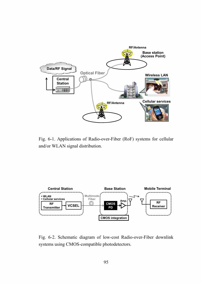
Data/RF Signal
CentralStation
RF/Antenna
Optical Fiber Wireless LAN
Base station(Access Point)
Cellular services
RF/Antenna
Fig. 6-1. Applications of Radio-over-Fiber (RoF) systems for cellular and/or WLAN signal distribution.
RFTransmitter VCSEL CMOS
PD
MultimodeFiber
RFReceiver
Amp.
Central Station Base Station Mobile Terminal
CMOS integration
WLANCellular services
Fig. 6-2. Schematic diagram of low-cost Radio-over-Fiber downlink systems using CMOS-compatible photodetectors.
95

6-2. RoF transmission of cellular or WLAN signal
6-2-1. Experimental setup for RoF transmission of WCDMA or WLAN signal
Using the CMOS-APD receiver, wideband code division multiple
access (WCDMA) or wireless local area network (WLAN) signal was
transmitted through RoF downlinks with experimental configuration
shown in Fig. 6-3. At the central station, optical modulation of 2.1-GHz
WCDMA or 5.2-GHz IEEE 802.11a WLAN signal was performed with
an 850-nm laser diode, an electro-optic modulator, and vector signal
generators (Agilent E4432 for WCDMA, Anritsu MG3700A for
WLAN). The generated optical signal was transmitted to the base
station via 3-m long multimode fiber whose core size is 50 μm. An 850-
nm optical attenuator was inserted between multimode fibers to control
input optical power into the CMOS-APD receiver. The base station was
simply configured with the CMOS-APD receiver and an 18-dB gain
amplifier (New Focus 1422). At the output of the base station, the
photodetected and amplified signal was radiated to free space using a 4-
dBi omnidirectional antenna. After 2-m wireless link, WCDMA or
WLAN signal was detected by another 4-dBi omnidirectional antenna,
amplified by a 24-dB gain low-noise amplifier (Mini-Circuit ZVA-
96

183+). For demodulation of WCDMA signal, the output of the low-
noise amplifier is directly connected to a vector signal analyzer
(Agilent 89600). On the other hand, for demodulation of WLAN signal,
frequency down-conversion was performed using 5-GHz, 7-dBm LO
signal and a RF mixer (Mini-Circuits ZMX-10G). To compensate the
conversion loss and satisfy the sensitivity of the vector signal analyzer,
an additional 20-dB gain amplifier (Mini-Circuits ZFL-1000LN) was
used. The frequency down-converted WLAN signal at 200 MHz is
demodulated by the vector signal analyzer.
Prior to experiments for RoF data transmission, characteristics of
the CMOS-APD receiver were investigated. Fig. 6-4 shows
photodetection frequency response of the CMOS-APD receiver. From
the measurement, it is observed that the 3-dB bandwidth of the CMOS-
APD receiver is less than carrier frequency of IEEE 802.11a WLAN
signal. To utilize the CMOS-APD receiver for 5-GHz band IEEE
802.11a WLAN signal detection, about 10-dB loss due to roll-off of
frequency response is inevitable.
97

CMOS-APDReceiver
AmplifierMultimode
Fiber
WirelessLink
Antenna
EOMLD PC
VSGWCDMA or WLAN
Central Station Base Station
LO
Amplifier
Mixer
Antenna
LNA
Mobile Terminal
VSA
VSA
2.1-GHz WCDMA
5.2-GHz 802.11aWLAN
LD: 850-nm Laser DiodePC: Polarization ControllerEOM: 20-GHz electro-optic modulatorAtt.: 850-nm optical attenuatorVSG: Vector Signal GeneratorVSA: Vector Signal AnalyzerLNA: Low-Noise AmplifierLO: Local Oscillator
Att.
Fig. 6-3. Experimental setup for RoF downlink data transmission of WCDMA or WLAN signal.
98

1E8 1E9 1E10-60
-50
-40
-30
-20
-10
0
10
20
Modulation frequency [Hz]
Nor
mal
ized
resp
onse
[dB
]
Popt = 0 dBm WCDMA 802.11aWLAN
Fig. 6-4. Photodetection frequency response of the CMOS-APD receiver used in the experiments. WCDMA and IEEE 802.11a signal bands are designated.
99

6-2-2. RoF transmission of WCDMA signal
First of all, WCDMA signal was transmitted through RoF downlink
based on the CMOS-APD receiver. Carrier frequency and chip rate of
WCDMA signal is 2.1 GHz and 4.096 Mc/s, respectively. To optimize
RoF system performance, dependences of rms EVMs on input RF
signal power to the electro-optic modulator was measured and the
result is shown in Fig. 6-5 (a). With increasing input WCDMA power,
rms EVM decreases at first and has the minimum value of about
3.26 % at the input signal power of -10 dBm due to the increased
optical modulation index. Beyond this condition, EVM starts to
increase. The degradation of EVM is due to inter-modulation distortion
caused by the nonlinearity of the electro-optic modulator.
To investigate the system performance dependent on the distance of
the fiber-optic link between central station and base station, the
dependence of EVM on input optical power into the CMOS-APD
receiver was also measured and the result is shown in Fig. 6-5 (b).
Because the 3GPP standard requires the EVM not to exceed 17.5 %, the
proposed RoF downlink using the CMOS-APD receiver satisfy the
EVM requirement in all the measured range of optical powers.
With the optimization of RoF downlink, WCDMA signal
transmission was performed. Fig. 6-6 shows output signal spectrum of
100

the CMOS-APD receiver when -4 dBm WCDMA signal was injected to
electro-optic modulator and -2 dBm optical signal was illuminated to
the CMOS-APD receiver. It is observed that photodetected WCDMA
signal has high SNR of about 30 dB. At the base station, transmitted
WCDMA signal through the RoF system and wireless link was
demodulated by the vector signal analyzer. Fig. 6-7 shows constellation
of demodulated WCDMA signal. In the experiment, rms EVM of
3.26 % is obtained. It is believed that this EVM value is sufficient for
downlink data transmission for WCDMA signal.
101

-25 -20 -15 -10 -5 0 5 10 15
3
4
5
6
7
8
9
10
11
Erro
r Vec
tor M
agni
tude
(%)
Input Signal Power (dBm)
WCDMA signalChip rate of 4.096 Mcps at 2.1 GHz
(a)
-8 -6 -4 -2 0 2
4
5
6
7
8
9
Erro
r Vec
tor M
agni
tude
(EVM
) [%
]
Input optical power (dBm)
WCDMA RoF transmissionFrequency: 2.1 GHz
(b)
Fig. 6-5. Dependence of error vector magnitude for demodulated WCDMA signal (a) on input RF power to the electro-optic modulator and (b) on input optical power to the CMOS-APD receiver at the base station.
102

2.095 2.100 2.105
-80
-70
-60
-50
-40
-30
-20RBW: 300 kHzVBW: 100 kHz
RF
pow
er [d
Bm
]
Frequency [GHz]
Fig. 6-6. Spectrum of WCDMA signal at the output of the CMOS-APD receiver in the base station.
EVM:3.26 %
WCDMA
Fig. 6-7. Constellation of demodulated WCDMA signal at the vector signal analyzer in the mobile terminal. EVM of 3.26 % is obtained.
103

6-2-3. RoF transmission of IEEE 802.11a WLAN signal
Through RoF downlink using the CMOS-APD receiver, IEEE
802.11a WLAN signal was transmitted. Carrier frequency and data rate
was set to 5.2 GHz and 54 Mbps, which is maximum data rate
supported by IEEE 802.11a, respectively. Fig. 6-8 (a) shows measured
rms EVM of demodulated WLAN signal as a function of input WLAN
signal power to the electro-optic modulator. The dependence of EVM
on the input signal power is similar to the WCDMA case. The
minimum rms EVM of 2.89 % was obtained at input WLAN power of -
4 dBm.
To estimate the supported optical link distance between central
station and base station, the dependence of EVM on input optical
power into the CMOS-APD receiver was also measured and the result
is shown in Fig. 6-8 (b). To meet the EVM requirement of 5.6 % for
IEEE 802.11a WLAN signal at 54 Mbps [48], optical power should be
higher than about -4 dBm. Accordingly, it is expected that the RoF
downlink using the CMOS-APD receiver can support a few hundred
meters of multimode fiber link, which has attenuation loss of less than
3 dB/km typically, with sufficient optical power sources.
Fig. 6-9 shows spectrum at the CMOS-APD receiver output when -
4 dBm WLAN signal was injected to the electro-optic modulator and 2
104

dBm optical signal was illuminated to the device. The photodetected
WLAN signal by the CMOS-APD receiver has SNR of about 25 dB.
After transmission of wireless link, the WLAN signal is demodulated
using the vector signal analyzer. Fig. 6-10 shows constellation of IEEE
802.11a 64-QAM OFDM WLAN signal at data rate of 54 Mbps. From
the measurement, rms EVM of 2.89 % was obtained.
105

-20 -15 -10 -5 0 5 102
3
4
5
6
7
8
9
10
11
Erro
r Vec
tor M
agni
tude
(%)
Input Signal Power (dBm)
WLAN signalOFDM 54 Mb/s at 5.2 GHz
(a)
-12 -10 -8 -6 -4 -2 0 2
3
4
5
6
7
8
9
10
Input optical power [dBm]
Erro
r Vec
tor M
agni
tude
(EVM
) [%
]
802.11a WLAN RoF transmissionFrequency: 5.2 GHz
5.6 %
(b)
Fig. 6-8. Dependence of error vector magnitude for demodulated WLAN signal (a) on input RF power to the electro-optic modulator and (b) on input optical power to the CMOS-APD receiver at the base station.
106

5.18 5.19 5.20 5.21 5.22-90
-80
-70
-60
-50
-40
RBW: 10 kHzVBW: 1 kHz
RF
pow
er [d
Bm
]
Frequency [GHz]
Fig. 6-9. Spectrum of IEEE 802.11a WLAN signal at the output of the CMOS-APD receiver in the base station.
EVM:2.89 %
WLAN
Fig. 6-10. Constellation of demodulated WLAN signal at the vector signal analyzer in the mobile terminal. EVM of 2.89 % is obtained.
107

6-3. Low-cost RoF downlinks for multi-standard signal transmission
6-3-1. Experimental setup for RoF transmission of both WCDMA and IEEE 802.11g WLAN signals
In order to realize cost-effective RoF systems, the CMOS-APD
receiver as well as a VCSEL and multimode fiber is employed for
feasibility demonstration. In addition, simultaneous RoF transmission
of multi-standard service for WCDMA and IEEE 802.11g is performed.
Fig. 6-11 shows the experimental setup for downlink RoF
transmission of multi-standard services. To generate optical signals, a
directly modulated 850-nm VCSEL was used at the central station. The
multi-standard signals, WCDMA at 2.1 GHz and WLAN at 2.4 GHz,
were generated using two separate vector signal generators (Agilent
E4432B, Anritsu MG3700A) and combined by a RF power combiner
(Mini-Circuits ZN2PD-63+). Modulated optical signals were
transmitted to the base station via 300-m long multimode fiber whose
core size was 50 μm. The measured optical transmission loss of 300-m
long multimode fiber was about 1.3 dB. Fig. 6-12 shows frequency
response of 300-m long multimode fiber. Owing to frequency roll-off
of 300-m long multimode fiber, high frequency RF signals can suffer
from additional loss of RoF link. At the base station, transmitted optical
108

signals were injected into the CMOS-APD receiver through a lensed
fiber, and after 24-dB amplification by an RF amplifier (Mini-Circuits
ZVA-183+), radiated by a 4-dBi omnidirectional antenna. After 2-m
wireless link, multi-standard RF signals were detected by another 4-dBi
omnidirectional antenna, amplified by a 24-dB gain low-noise amplifier,
and demodulated by a vector signal analyzer (Agilent 89600). In the
experiment, measured signal attenuation of 2-m wireless link including
antenna gains at 2-GHz band was about -40 dB. It is expected that the
wireless link distance can be extended with a high-gain power amplifier
to sufficiently compensate the loss.
109

850 nmVCSEL
CMOS-APDReceiver
PA
Central Station Base Station
Mobile Terminal
300 mMultimode
Fiber
2 mWireless link
Antenna
Antenna
VSG1
WCDMADemod. (VSA1) LNA
WLANDemod. (VSA2)
VCSEL: Vertical Cavity Surface Emitting Laser
VSG: Vector Signal GeneratorVSA: Vector Signal AnalyzerPA: Power AmplifierLNA: Low-Noise Amplifier
VSG2
WCDMA 802.11g WLAN
Fig. 6-11. Experimental setup for low-cost RoF downlink to transmit multi-standard signals of WCDMA and IEEE 802.11g WLAN.
0.0 2.0 4.0 6.0 8.0 10.0
-15
-10
-5
0
Freq
uenc
y re
spon
se [d
B]
Frequency [GHz]
300-m long MMF
Fig. 6-12. Measured frequency response of 300-m long multimode fiber (MMF).
110

6-3-2. Demonstration of multi-standard signals transmission
Both 2.1-GHz WCDMA and 2.4-GHz WLAN signals were applied
to the VCSEL and RoF transmitted. Fig. 6-13 shows the spectrum at the
output of the amplifier in the base station. Each of WCDMA and
WLAN RF signal powers was -5 dBm and the incident optical power at
the lensed fiber input was about -3 dBm. The measured signal-to-noise
ratio (SNR) was 44 dB for WCDMA, and 33 dB for WLAN signals as
shown in Fig 6-13 (b) and (c), respectively.
For investigation of signal interference between two types of
signals in the RoF downlink, the dependence of EVMs on interfering
signal powers was measured and the results are shown in Fig. 6-14. The
RF power of WCDMA or WLAN signals was set to -5 dBm while the
interferer power was scanned. The incident optical power at the input of
the lensed fiber was set to about -3 dBm.
As can be seen in the Fig. 6-14, WCDMA signal did not suffer any
interference from WLAN signals, whereas WLAN suffered when
WCDMA signal power became larger. This EVM degradation of
WLAN signal is believed due to saturation of the CMOS-APD receiver
and RF components in the base station. The IEEE 802.11g WLAN
signal with larger bandwidth is more sensitive to these undesired effects.
Nevertheless, the rms EVM of WLAN signal remains below the 5.6 %
111

requirement for data rate of 54 Mbps as specified in IEEE 802.11g
standard [49].
2.0 2.1 2.2 2.3 2.4 2.5-90
-80
-70
-60
-50
-40
-30
-20
-10
0
802.11g WLANWCDMA
RBW: 30 kHzVBW: 10 kHz
RF
pow
er [d
Bm
]
Frequency [GHz]
(a)
2.090 2.095 2.100 2.105 2.110
-80
-70
-60
-50
-40
-30
-20 RBW: 10 kHzVBW: 1 kHz
RF
pow
er [d
Bm
]
Frequency [GHz]
2.38 2.39 2.40 2.41 2.42
RBW: 10 kHzVBW: 1 kHz
Frequency (GHz)
(b) (c)
Fig. 6-13. (a) Spectrum of RoF transmitted multi-standard signals at the output of the CMOS-APD receiver. Enlarged spectrums of (b) WCDMA and (c) IEEE 802.11g WLAN signals.
112

-10 -9 -8 -7 -6 -52
3
4
5
6
7
8
9
10
Erro
r Vec
tor M
agni
tude
(EVM
) [%
]
WLAN signal power [dBm]
EVM of 4.096 Mcps WCDMA signalwith 802.11g WLAN signal transmission
(a)
-11 -10 -9 -8 -7 -6 -52
3
4
5
6
7
8
9
10
Erro
r Vec
tor M
agni
tude
(EVM
) [%
]
WCDMA signal power [dBm]
EVM of 802.11g 54 Mb/s WLAN signalwith WCDMA signal transmission
5.6 %
(b)
Fig. 6-14. EVM results of RoF transmission of multi-standard signals. (a) EVM of demodulated WCDMA signal as a function of WLAN signal power. (b) EVM of demodulated WLAN signal as a function of WCDMA signal power.
113

7. Summary
Recently, optical communication systems have evolved for short
distance access networks and optical interconnects to meet the demands
for high-capacity data transmission. For realization of these systems,
large numbers of optical components for wide deployment of the
systems is required, thus implementation cost becomes critical issue.
850-nm AlGaAs/GaAs VCSELs and multimode fiber have been
developed for low-cost optical transmitters and transmission medium,
however, cost-effective realization of optical receiver is still
challenging. To come up with this problem, CMOS technology has
been regarded as promising solution because photodetectors as well as
electronic circuits can be integrated on a single chip.
In this dissertation, CMOS-compatible avalanche photodetectors
(CMOS-APDs) to enable cost-effective optical receivers are
investigated. Using the CMOS-APDs, Gbps wireline data transmission
is performed, and utilization for fiber-fed 60-GHz self-heterodyne
wireless systems and low-cost radio-over-fiber systems are
demonstrated.
In chapter 2, difficulties and possible solutions for the realization of
high-performance CMOS-APDs are introduced. With TCAD
114

simulation results, the design consideration for the CMOS-APD is
explained. The structure of fabricated CMOS-APD is also described.
Chapter 3 shows characteristics of the fabricated CMOS-APD.
Measured DC and photodetection frequency response characteristics
are shown in this chapter. To clarify the physical origin of the rf-
peaking effect in photodetection frequency response, impedance
characteristics and equivalent circuit modeling is presented.
In chapter 4, 6.25-Gbps data transmission is demonstrated using the
CMOS-APD receiver having the CMOS-APD and a transimpedance
amplifier on a board. Experimental results for bit error rate (BER)
performance and eye diagram are presented.
For realization of fiber-fed millimeter-wave wireless systems in a
simple way, the self-heterodyne system is introduced in chapter 5.
Utilizing CMOS-APDs for the harmonic optoelectronic mixer (CMOS-
HOEM) and the self-oscillating harmonic optoelectronic mixer
(CMOS-SOHOM), simplified base stations are implemented. For the
feasibility demonstration, frequency up-conversion to 60-GHz band
and 25-Mbps 32-QAM data transmission through the fiber-fed 60-GHz
self-heterodyne wireless system are performed.
To reduce the cost of radio-over-fiber (RoF) systems, CMOS-APD
receivers are used for detection of optically modulated cellular and
115

WLAN applications. By adopting the CMOS-APD receiver in the base
station, single standard RoF transmission for 2.1-GHz WCDMA or 5.2-
GHz 802.11a WLAN is performed. In addition, low-cost RoF systems
having the CMOS-APD receiver, a VCSEL, and 300-m long multimode
fiber are proposed and simultaneous multi-standard signal transmission
for WCDMA and IEEE 802.11g are demonstrated.
From the results, it is expected that CMOS-APDs can play a central
role in future optical communication systems to achieve cost reduction
of optical receivers by enabling single chip integration with mature
CMOS technology.
116

References
[1] N. Savage, "Linking with light - high-speed optical interconnects," Spectrum, IEEE, vol. 39, pp. 32-36, 2002.
[2] M. R. Feldman, S. C. Esener, C. C. Guest, and S. H. Lee, "Comparison between optical and electrical interconnects based on power and speed considerations," Applied Optics, vol. 27, pp. 1742-1751, 1998.
[3] D. A. B. Miller, "Rationale and challenges for optical interconnects to electronic chips," Proceedings of the IEEE, vol. 88, pp. 728-749, 2000.
[4] Fiber Channel Industry Association (FCIA).[Online].Viewed 2008. Available:http:www.fiberchannel.org.
[5] Fiber Channel over Ethernet (FCoE).[Online].Viewed 2008. Available:http://fcoe.com.
[6] K. J. Ebeling, U. Fiedler, R. Michalzik, G. Reiner, and B. Weigl, "Recent advances in semiconductor vertical cavity lasers for optical communications and optical interconnects," in 22nd European Conference on Optical Communication, ECOC '96, 1996, pp. 81-88 vol.2.
[7] F. Koyama, "Recent Advances of VCSEL Photonics," Journal of Lightwave Technology, vol. 24, pp. 4502-4513, 2006.
[8] M. Jutzi, M. Grozing, E. Gaugler, W. Mazioschek, and M. Berroth, "2-Gb/s CMOS optical integrated receiver with a spatially Modulated photodetector," IEEE Photonics Technology Letters, vol. 17, pp. 1268-1270, 2005.
[9] Y. Kang, H.-D. Liu, M. Morse, M. J. Paniccia, M. Zadka, S.
117

Litski, G. Sarid, A. Pauchard, Y.-H. Kuo, H.-W. Chen, W. S. Zaoui, J. E. Bowers, A. Beling, D. C. McIntosh, X. Zheng, and J. C. Campbell, "Monolithic germanium//silicon avalanche photodiodes with 340 GHz gain-bandwidth product," Nature Photonics, vol. 3, pp. 59-63, 2009.
[10] P. Bhadri, P. Mal, S. Konanki, and F. R. Beyette, Jr., "Implementation of CMOS photodetectors in optoelectronic circuits," in The 15th Annual Meeting of the IEEE Lasers and Electro-Optics Society, 2002, pp. 683-684 vol.2.
[11] T. K. Woodward and A. V. Krishnamoorthy, "1-Gb/s integrated optical detectors and receivers in commercial CMOS technologies," IEEE Journal of Selected Topics in Quantum Electronics, vol. 5, pp. 146-156, 1999.
[12] H. Zimmermann and T. Heide, "A monolithically integrated 1-Gb/s optical receiver in 1-μm CMOS technology," IEEE Photonics Technology Letters, vol. 13, pp. 711-713, 2001.
[13] B. Yang, J. D. Schaub, S. M. Csutak, D. L. Rogers, and J. C. Campbell, "10-Gb/s all-silicon optical receiver," IEEE Photonics Technology Letters, vol. 15, pp. 745-747, 2003.
[14] S. Radovanovic, A. J. Annema, and B. Nauta, "A 3-Gb/s optical detector in standard CMOS for 850-nm optical communication," IEEE Journal of Solid-State Circuits, vol. 40, pp. 1706-1717, 2005.
[15] W. K. Huang, Y. C. Liu, and Y. M. Hsin, "A High-Speed and High-Responsivity Photodiode in Standard CMOS Technology," IEEE Photonics Technology Letters, vol. 19, pp. 197-199, 2007.
[16] W. K. Huang, Y. C. Liu, and Y. M. Hsin, "Bandwidth enhancement in Si photodiode by eliminating slow diffusion photocarriers," Electronics Letters, vol. 44, pp. 52-53, 2008.
118

[17] S. M. Sze, Physics of Semiconductor Devices, 2nd ed. New York: Wiley, 1981.
[18] H. Zimmermann, Integrated Silicon Optoelectronics. New York: Springer, 2000.
[19] S. R. Cho, S. K. Ynag, J. S. Ma, J. S. Yu, S. D. Lee, A. G. Choo, and T. I. Kim, "Investigations of Floating Guard Structures in a Planar InGaAs/InGaAsP/InP Avalanche Photodiode," Journal of Korean Physical Society, vol. 38, pp. 182-185, 2001.
[20] H. Finkelstein, M. J. Hsu, and S. C. Esener, "STI-Bounded Single-Photon Avalanche Diode in a Deep-Submicrometer CMOS Technology," IEEE Electron Device Letters, vol. 27, pp. 887-889, 2006.
[21] S. Wolf, Silicon Processing for the VLSI Era, Volume 1: Process Technology. Los Angeles: Lattice Press, 2000.
[22] D. S. Kim, S. R. Forrest, G. H. Olsen, M. J. Lange, R. U. Martinelli, and N. J. Di Giuseppe, "Avalanche gain in InAsyP1-y (0.1 < y < 0.3) photodetectors," IEEE Photonics Technology Letters, vol. 7, pp. 911-913, 1995.
[23] G. Kim, I. G. Kim, J. H. Baek, and O. K. Kwon, "Enhanced frequency response associated with negative photoconductance in an InGaAs/InAlAs avalanche photodetector," Applied Physics Letters, vol. 83, pp. 1249-1251, 2003.
[24] Y. C. Wang, "Small-signal characteristics of a Read diode under conditions of field-dependent velocity and finite reverse saturation current," Solid State Electronics, vol. 21, pp. 609-615, 1978.
[25] Y. Ahn, K. Han, and H. Shin, "A new physical RF model of junction varactors," Japanese Journal of Appliced Physics, vol. 42, pp. 2110-2113, 2003.
119

[26] M. Neuhauser, H. M. Rein, and H. Wernz, "Low-noise, high-gain Si-bipolar preamplifiers for 10 Gb/s optical-fiber links-design and realization," IEEE Journal of Solid-State Circuits, vol. 31, pp. 24-29, 1996.
[27] C.-S. Choi, H.-S. Kang, W.-Y. Choi, D.-H. Kim, and K.-S. Seo, "Phototransistors based on InP HEMTs and their applications to millimeter-wave radio-on-fiber systems," IEEE Transactions on Microwave Theory and Techniques, vol. 53, pp. 256-263, 2005.
[28] C.-S. Choi, J.-H. Seo, W.-Y. Choi, H. Kamitsuna, M. Ida, and K. Kurishima, "60-GHz bidirectional radio-on-fiber links based on InP-InGaAs HPT optoelectronic mixers," IEEE Photonics Technology Letters, vol. 17, pp. 2721-2723, 2005.
[29] J.-H. Seo, C.-S. Choi, Y.-S. Kang, Y.-D. Chung, J. Kim, and W.-Y. Choi, "SOA-EAM frequency up/down-converters for 60-GHz bi-directional radio-on-fiber systems," IEEE Transactions on Microwave Theory and Techniques, vol. 54, pp. 959-966, 2006.
[30] J.-H. Seo, Y.-K. Seo, and W.-Y. Choi, "1.244-Gb/s data distribution in 60-GHz remote optical frequency up-conversion systems," IEEE Photonics Technology Letters, vol. 18, pp. 1389-1391, 2006.
[31] H. Ogawa, D. Polifko, and S. Banba, "Millimeter-wave fiber optics systems for personal radio communication," IEEE Transactions on Microwave Theory and Techniques, vol. 40, pp. 2285-2293, 1992.
[32] P. Smulders, "Exploiting the 60 GHz band for local wireless multimedia access: prospects and future directions," IEEE Communications Magazine, vol. 40, pp. 140-147, 2002.
[33] R. L. Van Tuyl, "Unlicensed millimeter wave communications.
120

A new opportunity for MMIC technology at 60 GHz," in 18th Gallium Arsenide Integrated Circuit (GaAs IC) Symposium, 1996, pp. 3-5.
[34] M. Marcus and B. Pattan, "Millimeter wave propagation; spectrum management implications," IEEE Microwave Magazine, vol. 6, pp. 54-62, 2005.
[35] Y. Shoji, K. Hamaguchi, and H. Ogawa, "Millimeter-wave remote self-heterodyne system for extremely stable and low-cost broad-band signal transmission," IEEE Transactions on Microwave Theory and Techniques, vol. 50, pp. 1458-1468, 2002.
[36] Y. Shoji, K. Hamaguchi, and H. Ogawa, "A Low-Cost and Stable Millimeter-Wave Transmission System Using a Transmission-Filter-Less Double-Side-Band Millimeter-Wave Self-Heterodyne Transmission Technique," IEICE Transaction on Communications, vol. E86-B, pp. 1884-1892, 2003.
[37] Q. Z. Liu, R. Davies, and R. I. MacDonald, "Experimental investigation of fiber optic microwave link with monolithic integrated optoelectronic mixing receiver," IEEE Transactions on Microwave Theory and Techniques, vol. 43, pp. 2357-2360, 1995.
[38] G. Maury, A. Hilt, T. Berceli, B. Cabon, and A. Vilcot, "Microwave-frequency conversion methods by optical interferometer and photodiode," IEEE Transactions on Microwave Theory and Techniques, vol. 45, pp. 1481-1485, 1997.
[39] W. K. Kulczyk and Q. V. Davis, "The avalanche photodiode as an electronic mixer in an optical receiver," IEEE Trans. Electron Devices, vol. 19, pp. 1181-1190, 1972.
121

[40] A. J. Seeds and B. Lenoir, "Avalanche diode harmonic optoelectronic mixer," IEE Proceedings, vol. Pt. J, pp. 353-357, Dec. 1986.
[41] M. Y. W. Chia, B. Luo, M. L. Yee, and E. J. Z. Hao, "Radio over multimode fibre transmission for wireless LAN using VCSELs," Electronics Letters, vol. 39, pp. 1143-1144, 2003.
[42] A. Das, A. Nkansah, N. J. Gomes, I. J. Garcia, J. C. Batchelor, and D. Wake, "Design of low-cost multimode fiber-fed indoor wireless networks," IEEE Transactions on Microwave Theory and Techniques, vol. 54, pp. 3426-3432, 2006.
[43] T. Niiho, M. Nakaso, K. Masuda, H. Sasai, K. Utsumi, and M. Fuse, "Transmission performance of multichannel wireless LAN system based on radio-over-fiber techniques," IEEE Transactions on Microwave Theory and Techniques, vol. 54, pp. 980-989, 2006.
[44] T. Pak Kay, O. Ling Chuen, A. Alphones, B. Luo, and M. Fujise, "PER and EVM measurements of a radio-over-fiber network for cellular and WLAN system applications," Journal of Lightwave Technology, vol. 22, pp. 2370-2376, 2004.
[45] K. A. Persson, C. Carlsson, A. Alping, A. Haglund, J. S. Gustavsson, P. Modh, and A. Larsson, "WCDMA radio-over-fibre transmission experiment using singlemode VCSEL and multimode fibre," Electronics Letters, vol. 42, pp. 372-374, 2006.
[46] F. Tabatabai and H. Al-Raweshidy, "Performance Evaluation for WLAN and UWB Using Radio over Fibre," in The 9th European Conference on Wireless Technology, 2006, pp. 147-149.
[47] M. L. Yee, H. L. Chung, P. K. Tang, L. C. Ong, B. Luo, M. T.
122

Zhou, Z. Shao, and M. Fujise, "850nm Radio-Over-Fiber EVM Measurements for IEEE 802.11g WLAN and Cellular Signal Distribution," in 36th European Microwave Conference, 2006, pp. 882-885.
[48] Wireless LAN Medium Access Control (MAC) and Physical Layer (PHY) specifications: High-Speed Physical Layer in the 5 GHz Band, IEEE Standard 802.11a-1999, Part11, 1999.
[49] Wireless LAN Medium Access Control (MAC) and Physical Layer (PHY) specifications, IEEE Standard 802.11-2007, Part 11, 2007.
123

List of Publications
Journal Papers
[1] Hyo-Soon Kang, Myung-Jae Lee, and Woo-Young Choi, “Low-Cost Multi-Standard Radio-over-Fiber Downlinks Based on CMOS-Compatible Si Avalanche Photodetectors,” to be published in IEEE Photonics Technology Letters, 2009.
[2] Hyo-Soon Kang, Myung-Jae Lee, and Woo-Young Choi, “6.25-Gb/s Optical Receiver Using a CMOS-Compatible Si Avalanche Photodetector,” Journal of the Optical Society of Korea, vol. 12, no. 4, pp. 217–220, December 2008.
[3] Myung-Jae Lee, Hyo-Soon Kang, Kwang-Hyun Lee, and Woo-Young Choi, “Self-Oscillating Harmonic Optoelectronic Mixer Based on a CMOS-Compatible Avalanche Photodetector for Fiber-Fed 60-GHz Self-Heterodyne Systems,” IEEE Transaction on Microwave Theory and Techniques, vol. 56, no. 12, pp. 3180–3187, December 2008.
[4] Myung-Jae Lee, Hyo-Soon Kang, and Woo-Young Choi, “Equivalent Circuit Model for Si Avalanche Photodetectors Fabricated in Standard CMOS Process,” IEEE Electron Devices Letters, vol. 29, no. 10, pp. 1115–1117, October 2008.
[5] Hyo-Soon Kang, and Woo-Young Choi, "Fiber-supported 60 GHz self-heterodyne systems based on CMOS-compatible harmonic optoelectronic mixers," IEE Electronics letters, vol. 43, no. 20, pp. 1101–1103, September 27, 2007.
[6] Hyo-Soon Kang, Myung-Jae Lee, and Woo-Young Choi, "Si avalanche photodetectors fabricated in standard complementary
124

metal-oxide-semiconductor process," Applied Physics Letters, vol. 90, 151118, April 12, 2007.
[7] Chang-Soon Choi, Hyo-Soon Kang, Woo-Young Choi, Dae-Hyun Kim, and Kwang-Seok Seo, "Phototransistors based on InP HEMTs and their applications to millimeter-wave radio-on-fiber systems," IEEE Transactions on Microwave Theory and Techniques, vol. 53, no. 1, pp. 256–263, January 2005.
[8] Hyo-Soon Kang, Chang-Soon Choi, Woo-Young Choi, Dae-Hyun Kim, and Kwang-Seok Seo, "Characterization of phototransistor internal gain in metamorphic high-electron-mobility transistors," Applied Physics Letters, vol. 84, no. 19, pp. 3780–3782, May 2004.
[9] C.-S. Choi, H.-S. Kang, W.-Y. Choi, H.-J. Kim, W.-j. Choi, D.-H. Kim, K.-C. Jang, and K.-S. Seo, "High Optical Responsivity of InAlAs/InGaAs Metamorphic High-Electron Mobility Transistor on GaAs substrate with Composite Channels," IEEE Photonics Technology Letters, vol. 15, no. 6, pp. 846–848, June 2003.
[10] Chang-Soon Choi, Hyo-Soon Kang, Dae-Hyun Kim, Kwang-Seok Seo, and Woo-Young Choi, "60GHz Harmonic Optoelectronic Up-Conversion Using an InAlAs/InGaAs Metamorphic High-Electron-Mobility Transistor on a GaAs Substrate," Japanese Journal of Applied Physics, vol. 42, pp. L658–L659, June 2003.
International Conference Presentations
[1] Hyo-Soon Kang, Myung-Jae Lee, and Woo-Young Choi, “Multi-Standard Radio-over-Fiber Systems Using CMOS-Compatible Si
125

Avalanche Photodetectors,” IEEE Topical Meeting on Microwave Photonics, pp. 302–305 Gold Coast, Australia, September 30 – October 3, 2008.
[2] Woo-Young Choi, and Hyo-Soon Kang, "CMOS-Compatible Si Avalanche Photodetectors for Microwave Photonics Applications," Optoelectronics and Communications Conference (OECC), WeP-01, Sydney, Australia, July 7 – 10, 2008 (Invited Paper).
[3] Hyo-Soon Kang, Myung-Jae Lee, and Woo-Young Choi, "Radio-Over-Fiber Systems for WLAN Based on CMOS-Compatible Si Avalanche Photodetectors," IEEE MTT-S International Microwave Symposium (IMS), pp. 503–506, Atlanta, GA, USA, June 15 – 20, 2008.
[4] Myung-Jae Lee, Hyo-Soon Kang, Kwang-Hyun Lee, and Woo-Young Choi, "Fiber-Fed 60-GHz Self-Heterodyne Systems Using Self-Oscillating Harmonic Optoelectronic Mixers Based on CMOS-Compatible APDs," IEEE MTT-S International Microwave Symposium (IMS), pp. 587–590, Atlanta, GA, USA, June 15 – 20, 2008.
[5] Minsu Ko, Hyo-Soon Kang, and Woo-Young Choi, "A CMOS-Compatible Schottky-Barrier Diode Detector for 60-GHz Amplitude-Shift Keying (ASK) Systems," IEEE MTT-S International Microwave Symposium (IMS), pp. 1557–1560, Atlanta, GA, USA, June 15 – 20, 2008.
[6] Hyo-Soon Kang, Myung-Jae Lee, and Woo-Young Choi, "Characterization of Silicon Avalanche Photodetectors Fabricated in Standard CMOS process," The 7th Pacific Rim Conference on Lasers and Electro-Optics, pp. 614–615, COEX, Seoul, Korea, August 26 – 31, 2007.
[7] Hyo-Soon Kang, and Woo-Young Choi, "CMOS-compatible 60
126

GHz Harmonic Optoelectronic Mixer," IEEE MTT-S International Microwave Symposium (IMS), pp. 233–236, Honolulu, HI, USA, June 3 – 8, 2007.
[8] Hyo-Soon Kang, and Woo-Young Choi, "Millimeter-wave Optoelectronic Mixers Based on CMOS-Compatible Si Photodetectors," International Topical Meeting on Microwave Photonics, T1-5, Grenoble, France, October 4 – 6, 2006.
[9] Hyo-Soon Kang, and Woo-Young Choi, "Bias Voltage Optimization of Vertical PN-Junction Photodetectors Fabricated in Standard CMOS Technology," The 8th International Conference on Electronics, Information, and Communication, pp. 340–343, Ulaanbaatar, Mongolia, June 27 – 28, 2006.
[10] Woo-Young Choi, Chang-Soon Choi, Hyo-Soon Kang, Dae-Hyun Kim, and Kwang-Seok Seo, "Fiber-supported millimeter-wave data transmission systems based on InP HEMTs," The 6th Korea-Japan Joint Workshop on Microwave and Millimeter-wave Photonics, pp. 8–11, Gyeongju, Korea, January 27 – 28, 2005.
[11] Chang-Soon Choi, Hyo-Soon Kang, Dae-Hyun Kim, and Kwang-Seok Seo, and Woo-Young Choi "Characteristics of InP HEMT Harmonic Optoelectronic Mixers and Their Application to 60GHz Radio-on-Fiber Systems," IEEE MTT-S International Microwave Symposium, pp. 401–404, Fort Worth, TX, USA, June 5 – 11, 2004.
[12] Chang-Soon Choi, Hyo-Soon Kang, Dae-Hyun Kim, and Kwang-Seok Seo, and Woo-Young Choi "Millimeter-wave InP HEMT Optoelectronic Mixer," The 5th Japan-Korea Joint Workshop on Microwave and Millimeter-wave Photonics, pp. 19–22, Piazza ohmi Otsu, Shiga, Japan, January 29 – 30, 2004.
[13] Hyo-Soon Kang, Chang-Soon Choi, Woo-Young Choi, Dae-Hyun Kim, and Kwang-Seok Seo, "High Conversion Gain Millimeter-
127

wave Optoelectronic Mixer based on InAlAs/InGaAs Metamorphic HEMT," International Topical Meeting on Microwave Photonics, pp.105–108, Budapest, Hungary, September 10 – 12, 2003.
Domestic Conference Presentations
[1] Hyo-Soon Kang, Woo-Young Choi, "Radio-over-Fiber Systems for WLAN Using CMOS APD," The 15th Conference on Optoelectronics and Optical Communications (COOC), pp. 300-301, Busan Haeundae Hanwha Resort, May 14–16, 2008 (Invited Paper).
[2] Myung-Jae Lee, Hyo-Soon Kang, Kwang-Hyun Lee, Woo-Young Choi, "Fiber-supported 60 GHz-band Self-heterodyne Wireless Systems Using a Self-oscillating Harmonic Optoelectronic Mixer," The 15th Conference on Optoelectronics and Optical Communications (COOC), pp. 304-305, Busan Haeundae Hanwha Resort, May 14–16, 2008.
[3] Hyo-Soon Kang, Woo-Young Choi, "WLAN Radio-on-Fiber Systems Based on CMOS Compatible Avalanche Photodetectors," Photonics Conference, pp. 353-354, Jeju Poonglim Resort, November 14–16, 2007.
[4] Myung-Jae Lee, Hyo-Soon Kang, Woo-Young Choi, "An Equivalent Circuit Model for CMOS Compatible Avalanche Photodetectors," Photonics Conference, pp. 65-66, Jeju Poonglim Resort, November 14–16, 2007.
[5] Minsu Ko, Hyo-Soon Kang, Woo-Young Choi, "0.18-um CMOS Schottky Barrier Diodes for 60-GHz Self-Heterodyne Systems,"
128

Autumn Conference on Microwave and Wave Propagation, pp. 471-474, Cheju National University, September 13–14, 2007.
[6] Hyo-Soon Kang, Myung-Jae Lee, Woo-Young Choi, "Photodetection Frequency Response Peaking in Si Avalanche Photodetectors Fabricated in Standard CMOS Process," The 14th Conference on Optoelectronics and Optical Communications (COOC), pp. 110-111, Jeju Hanwah Resort, May 16–18, 2007.
[7] Hyo-Soon Kang, Woo-Young Choi, "60 GHz Harmonic Optoelectronic Mixers Based on CMOS-compatible Si APD," Photonics Conference, pp. 314-315, Sorak Daemyung Resort, November 8–10, 2006.
[8] Hyo-Soon Kang, Woo-Young Choi, "Bias Voltage Optimization of Vertical PN-Junction Photodetectors Fabricated in Standard CMOS Technology," The 13th Conference on Optoelectronics and Optical Communications (COOC), pp. 213-214, Bugok Ilsung Condominium, May 10–12, 2006.
[9] Chang-Soon Choi, Hyo-Soon Kang, Dea-Hyun Kim, Kwang-Seok Seo, Woo-Young Choi, "Fiber-optic/60GHz broadband transmission systems using InP HEMT phototransistors," The 11th Conference on Optoelectronics and Optical Communications (COOC), pp.283-284, Information and Communications University, May 12–13, 2004.
[10] Hyo-Soon Kang, Chang-Soon Choi, Woo-Young Choi, Kyoungchul Jang, Kwang-Seok Seo, "Photodetection Characteristics of InAlAs/InGaAs/InP HEMT," Optical Society of Korea Annual Meeting, pp. TF-V6, Inha University, February 13–14, 2003.
[11] Hyo-Soon Kang, Chang-Soon Choi, Woo-Young Choi, Joo-Hiuk Son, Kyungchul Jang, Kwang-Seok Seo, "Photodetection of 1.55 modulated lightwave in InP HEMT," Photonics Conference,
129

pp. 719-720, Yongpyong Resort, October 30 – November 1, 2002.
[12] Chang-Soon Choi, Hyo-Soon Kang, Woo-Young Choi, Hwe-Jong Kim, Won-Jun Choi, Kyungchul Jang, Dae-Hyun Kim, Kwang-Seok Seo, "Photoresponse of InAlAs/InGaAs Metamorphic HEMT on GaAs substrate with Composite Channel," Photonics Conference, pp. 723-724, Yongpyong Resort, October 30 – November 1, 2002.
[13] Chang-Soon Choi, Hyo-Soon Kang, Young-Kwang Seo, Jun-Hyuk Seo, Woo-Young Choi, Kyungchul Jang, Dae-Hyun Kim, Kwang-Seok Seo, "60GHz Broadband Up-conversion using Metamorphic HEMT as a Harmonic Optoelectronic Mixer," Photonics Conference, pp. 83-84, Yongpyong Resort, October 30 – November 1, 2002.
130

131
Patents
[1] Hyo-Soon Kang, and Woo-Young Choi, “Optoelectronic Mixer Based on CMOS and Base Station Using the Same,” Korean Patent, Patent No. 10-0789364, December 20, 2007.
[2] Hyo-Soon Kang, Kwang-Hyun Lee, and Woo-Young Choi, “Wireless Communication System Having CMOS Structure and Method of Manufacturing the Same,” Korean Patent, Patent No. 10-0829117, May 6, 2008 PCT Patent, Application No. PCT/KR2007/000928, February 22, 2007.