class # 02 february 01, 2011 dohn bowden
TRANSCRIPT

Microprocessors B (17.384)
Spring 2011
Lecture Outline
Class # 02
February 01, 2011
Dohn Bowden
1
Today’s Lecture
• Administrative
• Microcontroller Hardware and/or Interface
• Programming/Software
• Lab
• Homework
2

Course Admin
3

Administrative
• Admin for tonight …
– Syllabus Highlights
• Lab #1 is in two weeks (February 15th)
– We shall perform Lab #1 next week … NO lecture
4

Syllabus ReviewWeek Date Topics Lab Lab Report Due
1 01/25/11 PIC pin out, C programming, Watchdog Timer, Sleep
2 02/01/11 General-purpose IO, LED/switch IO, FSM 1
3 02/08/11 Lab 1 con’t
4 02/15/11 Interrupts, Timers, interrupt-driven IO 2 1
5 02/22/11 Lab 2 con’t
6 03/01/11 Asynchronous and Synchronous Serial IO (UART, I2C, SPI)
3 2/ / SPI)
7 03/08/11 Examination 1
X 03/15/11 No Class – Spring Break
8 03/22/11 Lab 3 con’t8 03/22/11 Lab 3 con’t
9 03/29/11 Serial EEPROM operation, DAC, DC motor control, Servos, Stepper motor control 4 3
10 04/05/11 Lab 4 con’t
11 04/12/11 Advanced Hardware Topics Project 4
12 04/19/11 Examination 2
13 04/26/11 Work on Course Project Project
5
14 05/03/11 Final Exam/Course Project Brief and Demonstration Demo

Access to Labs
• To gain access to BL-407
– You will need to have an access cards
– Access cards are given out on the South Campus at Access Services
• Arrangements are done through the Continuing Education Office
– I need your UMS# (will be on your Access Card) for room access
6

Course Web Site
• The Course Web site Homepage is at:
htt //f lt l d /db dhttp://faculty.uml.edu/dbowden
• Any issues?
7

Email Distribution List
• For those who have sent me your email address or addresses at …
• I sent a test email to you
8

Chat Page
• Still looking into what is available through the school
– More to follow as it develops
9

MicrocontrollerHardwareand / or
Interfaces
10

Template Sheet
11

Chapter 8Chapter 8 …
continued …
12

Parallel Port Operation
13

General Purpose Input/Output (I/O)
• The simplest type of I/O via the PIC24 external pins are …
– Parallel I/O (PIO) ports
• A PIC24 family can have multiple PIO ports named …
– PORTA, PORTB, PORTC, PORTD, etc
• Each is 16-bits, and the number of PIO pins depends on the particular PIC24 and package.particular PIC24 and package.
14

General Purpose Input/Output (I/O)
• The PIC24HJ32GP202/28 pin package has …
– PORTA• Bits … RA4 through RA0
– PORTB• Bits … RB15 through RB0g
• Generically referred to as … PORTx
15

General Purpose Input/Output (I/O)
• Each pin on PORTx can either be …
– An input … or …– An output
• Data direction is controlled by …
– The corresponding bit in the …• TRISx registers
– ‘1’ = input1 = input– ‘0’ = output
Th LAT i h ld h l l i PORT• The LATx register holds the last value written to PORTx16

PORT B example …
17

PORT B Example
18

PORT B Example … continued
19

Switches …
20

21

PORTx and LATx …
22

23

LATx versus PORTx
• Writing LATx is the same as …
– Writing PORTx
• Both writes go to the latch
• Reading LATx …g– Reads the latch output …
• The last value written
• Reading PORTx …– Reads the actual pin value
24

LATx versus PORTx … continued
• Configure RB3 as an open-drain output … then write a ‘1’ to it
– Open-drain … means that the PMOS pull-up is disabled• Removing the ability of the port pin to drive it’s output high
– Output pin floats when driven high
• The physical pin is tied to ground, so it can never go highg g g
• Reading _RB3 returns a ‘0’ … but reading _LATB3 returns a ‘1’ … the last value writtenthe last value written
25

LATx versus PORTx … continued
• If we have the following two “C” statements consecutively …
_RB2 = 1; _RB3 = 1;
• An incorrect assignment for the second assignment can occur– Per the datasheet …
• Depends on external pin loading … and …• Internal clock speed• Internal clock speed
• x
26

LATx versus PORTx … continued
• Therefore use the following two “C” statements vice previous …
_LATB2 = 1; _LATB3 = 1;
• We therefore will use …– LATxy …
• For port writes
– And RBxyAnd … RBxy …• For reading a pin state
27

LATx versus PORTx … continued
• Why does the previous occur?
– When the compiler coverts from “C” to assembly
28

TRI-State Buffer …
29

Tri-State Buffer (TSB) Review
• A tri-state buffer (TSB) has … – Input– Input …– Output … and … – Output enable (OE) pins
• Output can either be … – ‘1’ …– ‘0’ … or …– ‘Z’ (high impedance)
30

Bidirectional Data Link …
31

Bidirectional Data Link
• Uses one wire
• Data is flowing either from …
– CPU_a to CPU_b … or …
– CPU_b to CPU_a
• But … NEVER … both directions at the same time …
– Can cause an indeterminate voltage and programming error
32

Bidirectional Data Link
33

Schmitt Trigger Input Buffer …
34

Schmitt Trigger Input Buffer
• Each PIO input has a Schmitt trigger input buffer … – This transforms slowly rising/falling input transitions into– This transforms slowly rising/falling input transitions into …
• Sharp rising/falling transitions internally
35

PORTx …
36

PORTx Shared Pin Functions
• External pins are shared with other on-chip modules
• Just setting _TRISx = 1 may be not be enough to configure a PORTx pin as an input
– Depending on what other modules share the pin …
37

PORTx Shared Pin Functions
• RB15 is shared with … AN9– Which is an analog input to the on-chip Analog-to-Digital– Which is an analog input to the on-chip Analog-to-Digital
Converter (ADC)
We must disable the Analog to Digital Converter• We must disable the Analog-to-Digital Converter
38

PORTx Shared Pin Functions
39

PORTx Shared Pin Functions
• _PCFG9 … controls AN9 which shares same pin as RB15
– Register 18-7 (datasheet)• “1” --- Digital mode• “0” --- Analog mode
40

Analog/Digital Pin versus Digital-only PinDigital-only Pin …
41

Analog/Digital Pin versus Digital-only Pin
• Pins with shared analog/digital functions have a maximum input voltage of …voltage of …
• Vdd + 0.3 V … therefore … 3.6 V
• Pins with no analog functions (“digital-only” pins) are …
• 5 V tolerant … their maximum input voltage is … 5.6 V
– Can receive digital inputs from 5V componentsCan receive digital inputs from 5V components
42

Analog/Digital Pin versus Digital-only Pin
• Most PIO pins can only source or sink a maximum of …
• 4 mA
• You may damage the output pin if you …
– Tie a load that tries to sink/source more than 4 mA
43
Internal Weak Pull-ups …
44

Internal Weak Pull-ups
• CN pins …
– Input Change Notification interrupt pins …
• Will be discussed in detail later in the semester
45
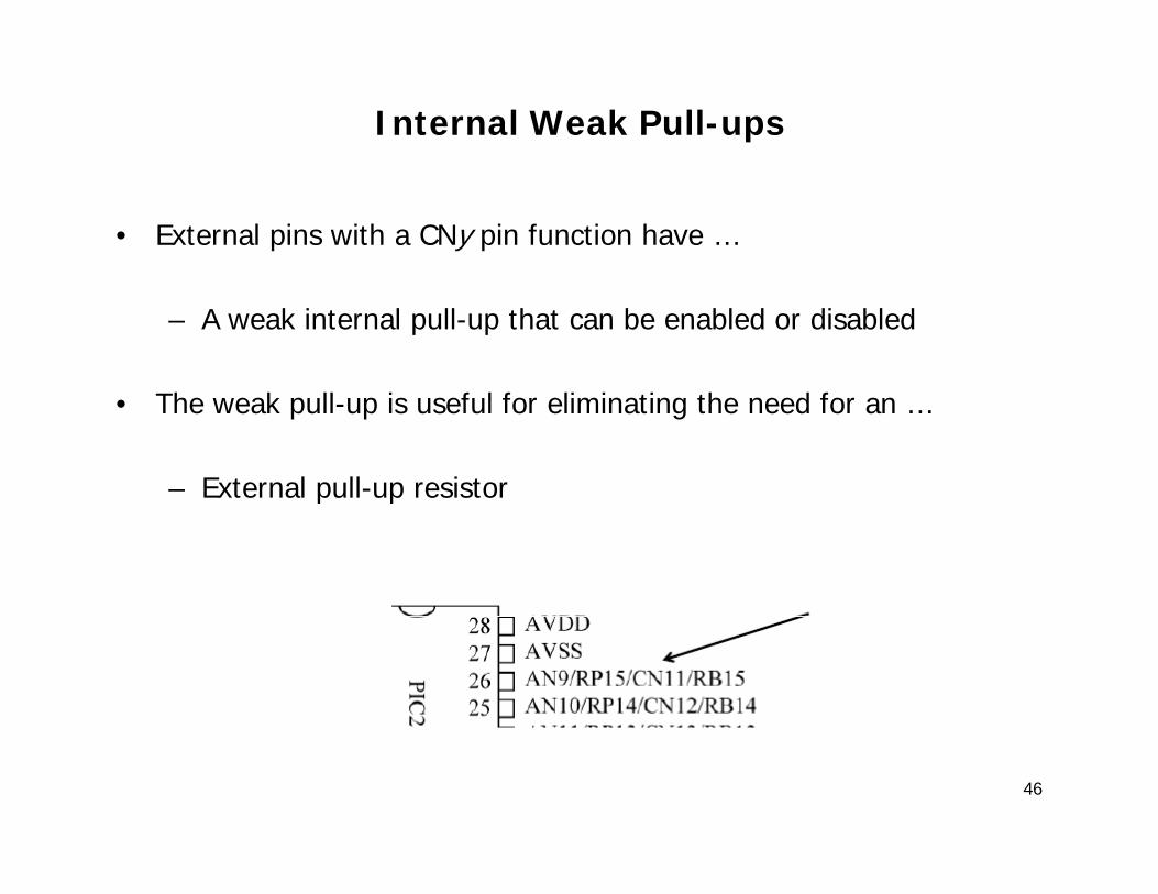
Internal Weak Pull-ups
• External pins with a CNy pin function have …
– A weak internal pull-up that can be enabled or disabled
• The weak pull-up is useful for eliminating the need for an …
– External pull-up resistor
46

Internal Weak Pull-ups
• For example … when connecting a switch
• Change notification input … to enable pull-up …» CN11PUE = 1;» CN11PUE = 1;
• To disable pull-up …CN11PUE 0» CN11PUE = 0;
47

Internal Weak Pull-ups
• CN11PUE …
– Datasheet …Table 4-2
48

Open Drain Outputs …
49

Open Drain Outputs
• Open-drain … means that the PMOS pull-up is disabled
– Removing the ability of the port pin to drive it’s output high
– Output pin floats when driven high
• Each PIO pin can be configured as an open drain output …g
– Which means the pull-up transistor is disabled
50

Open Drain Outputs
51

Port Configuration Macros …
52

Port Configuration Macros
• For convenience, we supply macros/inline functions that hide pin configuration details …configuration details …
53
Port Configuration Macros
• These macros are supplied for each port pin
• These functions change depending on the particular PIC24 … therefore the …
– include/devices directory
• Has a include file for each PIC24 … and … the correct file is included by the include/pic24_ports.h file
• NOTE … the include/devices directory is the directory of the material supplied with the textbook, not the compiler
54

Other Port Configuration Macros
• Other macros are provided for pull-up and open drain configurations …configurations …
55

Other Port Configuration Macros
• General forms are …» ENABLE Rxy PULLUP()» ENABLE_Rxy_PULLUP()» DISABLE Rxy PULLUP() ENABLE Rxy OPENDRAIN()» DISABLE_Rxy_PULLUP()» ENABLE_Rxy_OPENDRAIN()» DISABLE_Rxy_OPENDRAIN()» CONFIG_Rxy_AS_DIG_OD_OUTPUT()
• A port may not have a pull-up if it does not share the pin with a change notification input …change notification input … – In this case the macro does not exist and you will get an error
compile the code message when you try to code
56

Configuration Macros
• Configuration Macros …
– You may want to initially write your code without using macros …
• To become familiar with how to perform the actual functions
57

Programming/Softwareg g
58

Flashing LED1…
59

Flashing LED1
• Our initial hardware/software problem will be to flash LED1
60

Flashing LED1
• The textbook provides a solution to the problem of flashing LED1
– It provides advanced programming techniques … which …
• Will reduce code … but …
– Adds complexity for the novice “C” programmerg
• I recommend …
– Reviewing the Code to understand what is being performed– Write the code to your knowledge level
61

Flashing LED1
• We can …
– Utilize the provided code … or …
– Utilize the methods from last semester … or …
– A combination of both …
• Take the best from each
– And … what you understand!
62

LEDflash.c …
63

LEDflash.c
64

65

I/O Configuration
• Use macros to isolate pin assignments for physical devices so …
– It is easy to change code if (WHEN!) the pin assignments change!
66

Counting # of Press/Releases
67

Additional Code and Devices …
68

Additional Code and Devices
• Chapter 8 contains excellent material that you should consider using when designing your devices …when designing your devices …
– State Machine for LED toggling
– LED/switch I/O problem
– Interfacing to an LCD Module• Contains …
– Schematic– LCD commands
LCD Code examples– LCD Code examples
69

Summary …
70

Summary
• General Purpose Input / Output (GPIO) port usage of …
» PORTA, PORTB
• Weak pull-ups of PORTB
• Schmitt Triggergg
• Tri-state buffers
• Open-drain output
W i i C d f fl hi d LED d LED/S i h IO• Writing C code for flashing and LED and LED/Switch IO71

Lab
72

Peer Review of Software …
73

Peer Review of Software Developed
• Next week!!!
– Be prepared
• How you wrote your code
• Problems encountered
• Questions you need solved
74

Lab #1 …
75

Lab #1
• Initial breadboard wiring
• Initial processor start-up
• Initial processor software development
– Flashing LED1g
– Switch interface
76

Next Class
77

Next Class Topics
• Lab #1 continued
78

Homework
79

Homework
• Read … – Material covered in today’s lecture (may want to re-read)– Material covered in today s lecture (may want to re-read) …
• Chapter 8, pages 287 – 312
– Material for lecture in two weeks …• Chapter 9, pages 317 - 362
• Work on Lab#1– Breadboard wiring– Code developmentCode development
80

Ti t t tTime to start the labthe lab …
81

Lab
• Start Lab #1 …
82

References
83
References
1. None
84