cis 4930 digital system testing logic simulationhaozheng/teach/psv/slides/3-logicsimulation.pdf ·...
TRANSCRIPT
CIS 4930 Digital System TestingLogic Simulation
Dr. Hao ZhengComp Sci & Eng
U of South Florida
Overview• What is Logic Simulation?• Types of Simulation– Compiled Simulation– Event Driven Simulation
• Delay models• Hazards
2
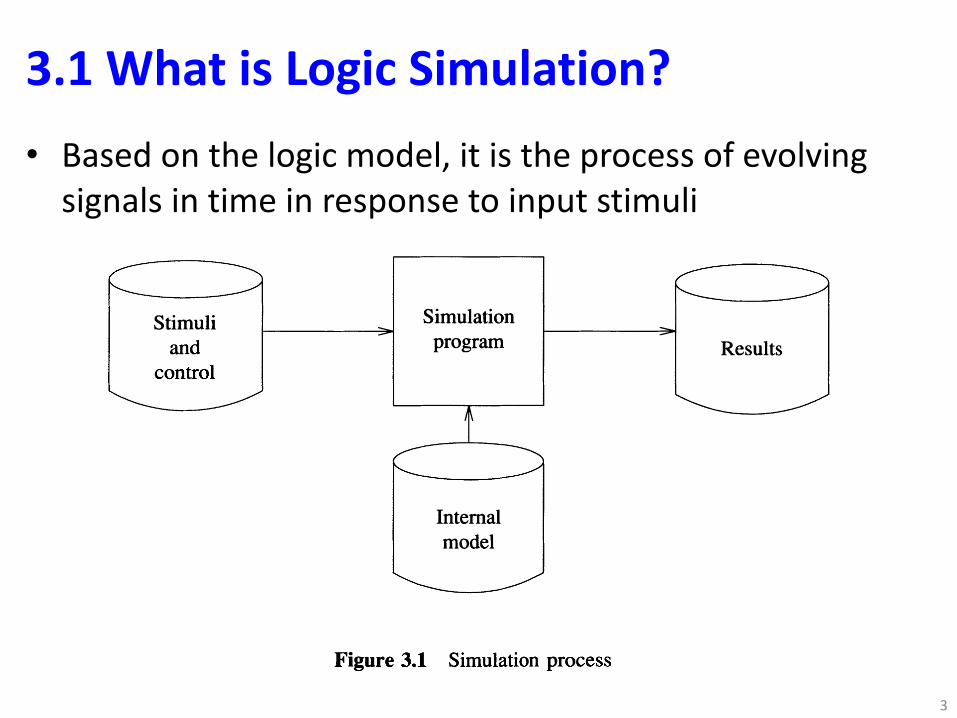
3.1 What is Logic Simulation?• Based on the logic model, it is the process of evolving
signals in time in response to input stimuli
3
3. LOGIC SIMULATION
About This Chapter
First we review different aspects of using logic simulation as a tool for designverification testing, examining both its usefulness and its limitations. Then weintroduce the main types of simulators, compiled and event-driven. We analyze severalproblems affecting the accuracy and the performance of simulators, such as treatmentof unknown logic values, delay modeling, hazard detection, oscillation control, andvalues needed for tristate logic and MOS circuits. We discuss in detail techniques forelement evaluation and gate-level event-driven simulation algorithms. The last sectiondescribes special-purpose hardware for simulation.
3.1 ApplicationsLogic simulation is a form of design verification testing that uses a model of thedesigned system. Figure 3.1 shows a schematic view of the simulation process. Thesimulation program processes a representation of the input stimuli and determines theevolution in time of the signals in the model.
Stimuliand
control
Simulationprogram
Internalmodel
Figure 3.1 Simulation process
Results
The verification of a logic design attempts to ascertain that the design performs itsspecified behavior, which includes both function and timing. The verification is doneby comparing the results obtained by simulation with the expected results provided bythe specification. In addition, logic simulation may be used to verify that the operationof the system is
39
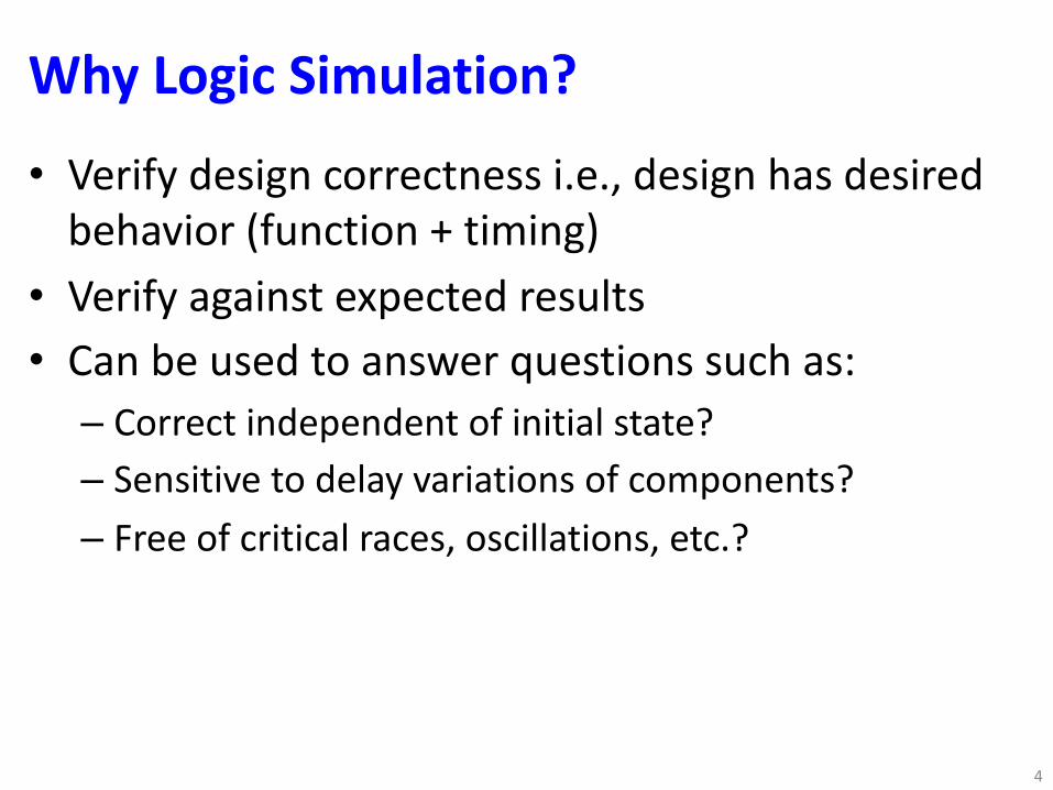
Why Logic Simulation?• Verify design correctness i.e., design has desired
behavior (function + timing)• Verify against expected results• Can be used to answer questions such as:– Correct independent of initial state?– Sensitive to delay variations of components?– Free of critical races, oscillations, etc.?
4

Why Logic Simulation?...contd.,• We can also use it to:– Evaluate design alternatives– Evaluate proposed changes– Documentation (timing diagrams)
• Against a prototype, simulation has following advantages:– Checking various error conditions– Ability to change delays in the model– Start the simulated circuit in any desired state– Precise control of timing of async events (interrupts)– Automated testing
5
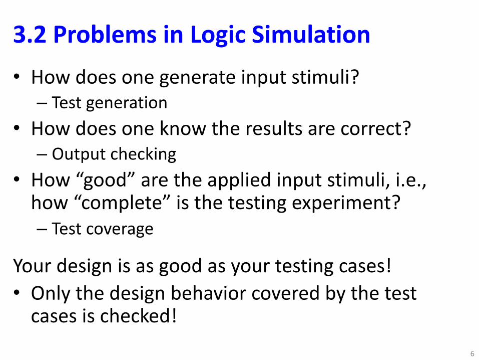
3.2 Problems in Logic Simulation• How does one generate input stimuli?– Test generation
• How does one know the results are correct?– Output checking
• How “good” are the applied input stimuli, i.e., how “complete” is the testing experiment?– Test coverage
Your design is as good as your testing cases!• Only the design behavior covered by the test
cases is checked!6
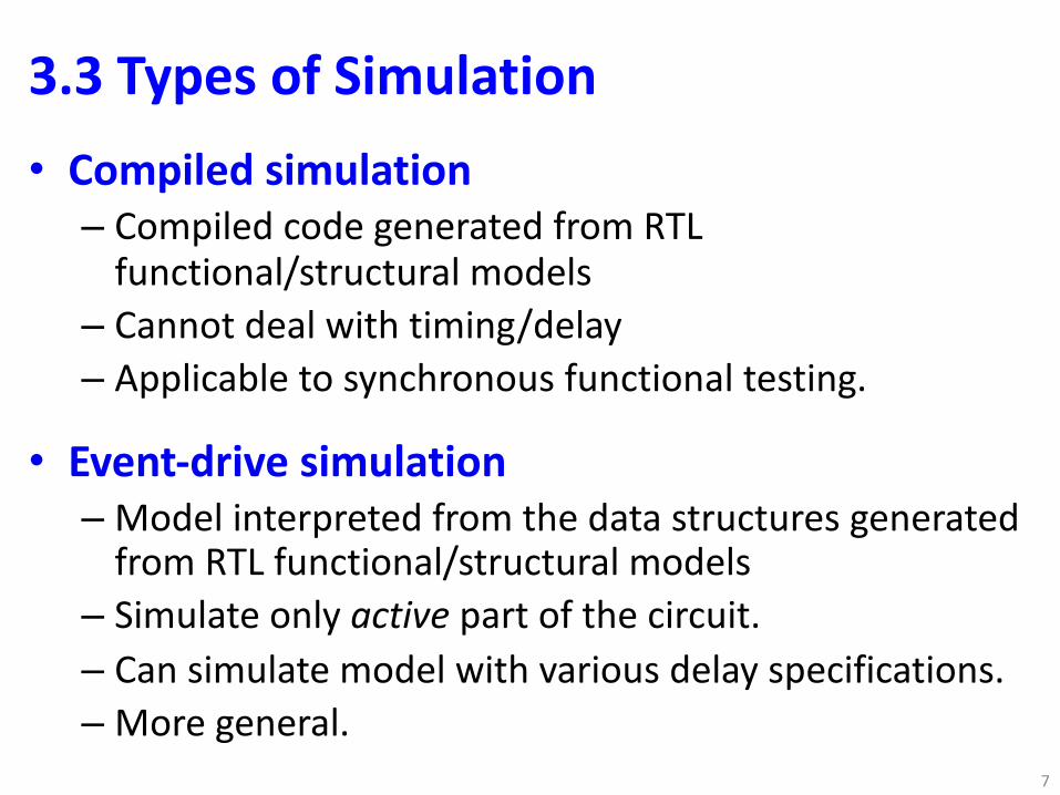
3.3 Types of Simulation• Compiled simulation– Compiled code generated from RTL
functional/structural models– Cannot deal with timing/delay– Applicable to synchronous functional testing.
• Event-drive simulation– Model interpreted from the data structures generated
from RTL functional/structural models– Simulate only active part of the circuit.– Can simulate model with various delay specifications.– More general.
7

3.4 The Unknown Logic Value• When a circuit is powered on, initial state of FFs
and RAMs is unpredictable.• Special logic value, u, to indicate unknown logic
value– need to extend Boolean operators to 3-valued logic
• u represents one value in set {0,1}• 0 and 1 represented by sets {0}, {1} respectively
8
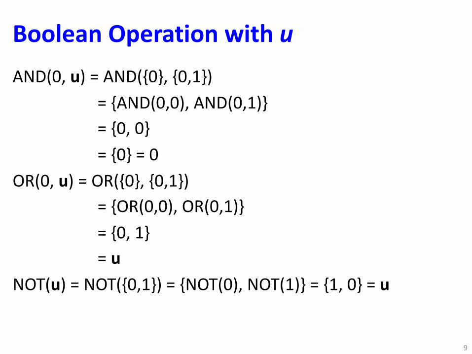
Boolean Operation with uAND(0, u) = AND({0}, {0,1})
= {AND(0,0), AND(0,1)}= {0, 0}= {0} = 0
OR(0, u) = OR({0}, {0,1})= {OR(0,0), OR(0,1)}= {0, 1}= u
NOT(u) = NOT({0,1}) = {NOT(0), NOT(1)} = {1, 0} = u
9
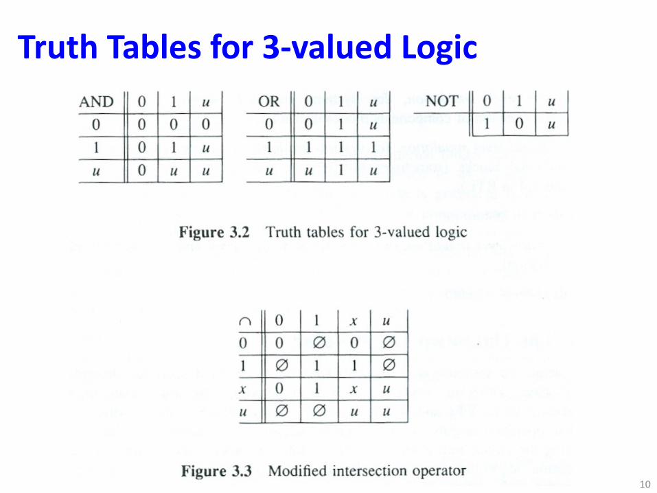
Truth Tables for 3-valued Logic
10
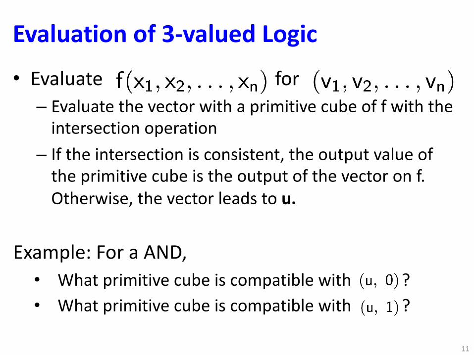
Evaluation of 3-valued Logic
11
• Evaluate for– Evaluate the vector with a primitive cube of f with the
intersection operation– If the intersection is consistent, the output value of
the primitive cube is the output of the vector on f. Otherwise, the vector leads to u.
Example: For a AND, • What primitive cube is compatible with ?• What primitive cube is compatible with ?
The Unknown Logic Value
oU
U
U
45
UU
1
Figure 3.4 Pessimistic result in 3-valued simulation
when we have only one state variable set to u. Figure 3.5 illustrates how the use of uand ii may lead to incorrect results. Since it is better to be pessimistic than incorrect,using u and u is not a satisfactory solution. A correct solution would be to use severaldistinct unknown signals u 1, U 2, ... , Uk (one for every state variable) and the rulesUi,Ui=O and ui+ui=l. Unfortunately, this technique becomes cumbersome for largecircuits, since the values of some lines would be represented by large Booleanexpressions of Ui variables.
Q
Q
Q
Q
U
U
o
Figure 3.5 Incorrect result from using U and Ii
Often the operation of a functional element is determined by decoding the values of agroup of control lines. A problem arises in simulation when a functional elementneeds to be evaluated and some of its control lines have u values. In general, ifk control lines have u values, the element may execute one of 2k possible operations.An accurate (but potentially costly) solution is to perform all 2k operations and to takeas result the union set of their individual results. Thus if a variable is set to 0 in someoperations and to 1 in others, its resulting value will be {O,l} = u. Of course, this
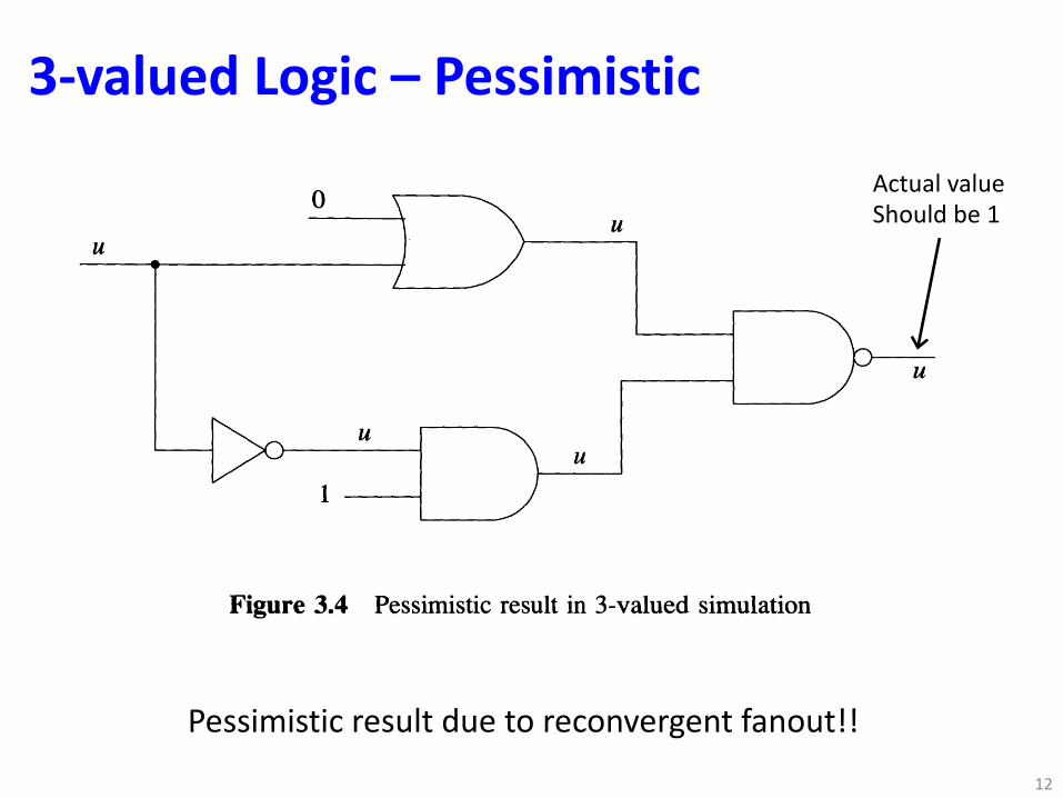
3-valued Logic – Pessimistic
12
Actual valueShould be 1
Pessimistic result due to reconvergent fanout!!
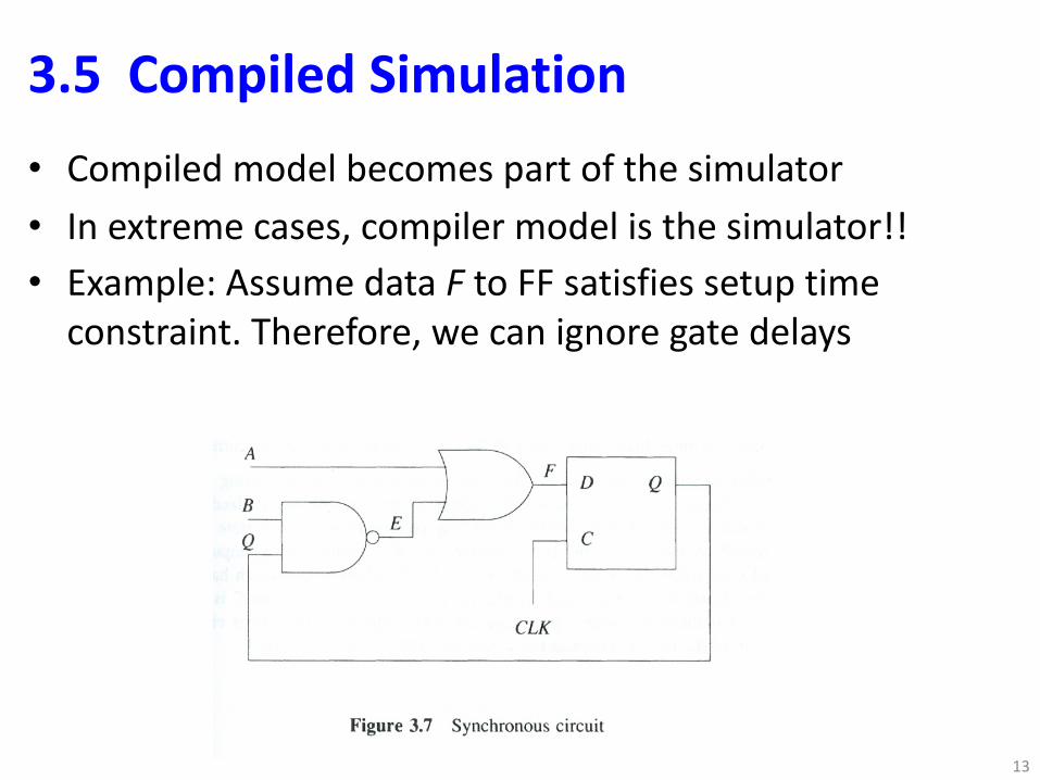
3.5 Compiled Simulation• Compiled model becomes part of the simulator• In extreme cases, compiler model is the simulator!!• Example: Assume data F to FF satisfies setup time
constraint. Therefore, we can ignore gate delays
13
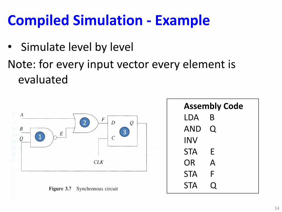
Compiled Simulation - Example• Simulate level by levelNote: for every input vector every element is
evaluated
14
Assembly CodeLDA BAND QINVSTA EOR ASTA FSTA Q
1
23
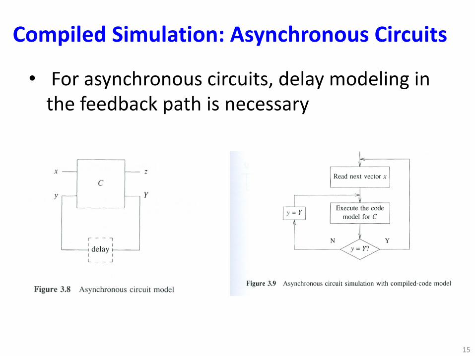
Compiled Simulation: Asynchronous Circuits
15
• For asynchronous circuits, delay modeling in the feedback path is necessary
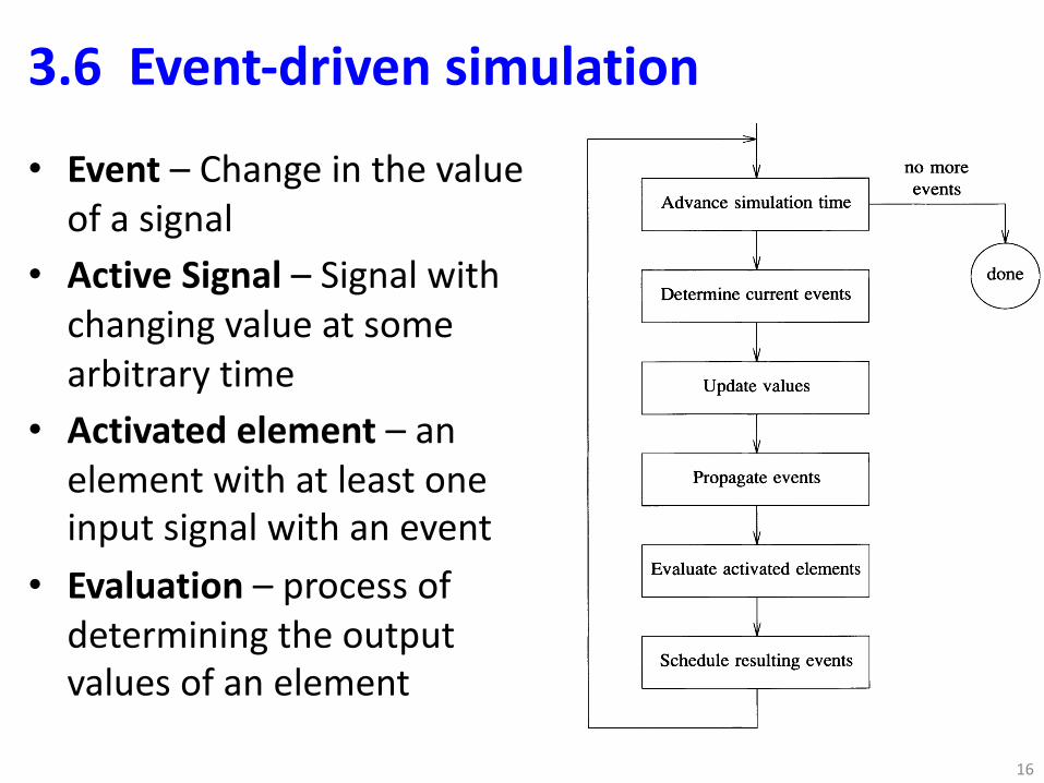
3.6 Event-driven simulation• Event – Change in the value
of a signal• Active Signal – Signal with
changing value at some arbitrary time
• Activated element – an element with at least one input signal with an event
• Evaluation – process of determining the output values of an element
16
Event-Driven Simulation
no moreevents
Advance simulation time
doneDetermine current events
Update values
Propagate events
Evaluate activated elements
Schedule resulting events
Figure 3.12 Main flow of event-driven simulation
51
simulator has periodically to read the stimulus file and to merge the events on theprimary inputs with the events internally generated.
In addition to the events that convey updates in signal values, an event-drivensimulator may also process control events, which provide a convenient means toinitiate different activities at certain times. The following are some typical actionsrequested by control events:
• Display values of certain signals.
• Check expected values of certain signals (and, possibly, stop the simulation if amismatch is detected).
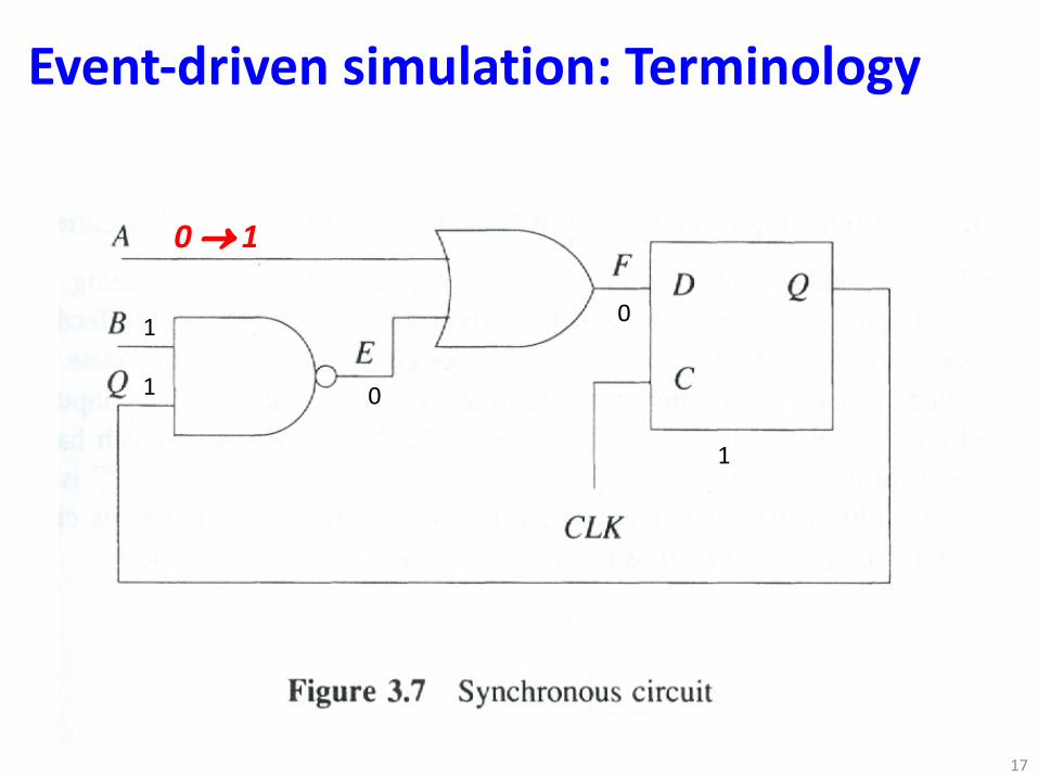
Event-driven simulation: Terminology
17
0 ® 1
1
1
0
01
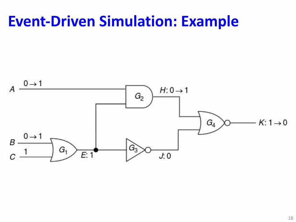
Event-Driven Simulation: Example
18
Wang, Laung-Terng, Wu, Cheng-Wen, and Wen, Xiaoqing. Morgan Kaufmann Series in Systems on Silicon : VLSI Test Principles and Architectures : Design for Testability (1). Burlington, US: Morgan Kaufmann, 2006. ProQuest ebrary. Web. 4 January 2017.Copyright © 2006. Morgan Kaufmann. All rights reserved.
Event-Driven Simulation• Uses structural model to propagate events• Stimulus file – changes in the values on primary
inputs• Events on other lines are produced by evaluations
of activated elements• Event occurs at a certain (simulated) time• Applied stimuli – event sequences in time• Can have events scheduled in future i.e., pending
events• Simulator maintains an event list
19
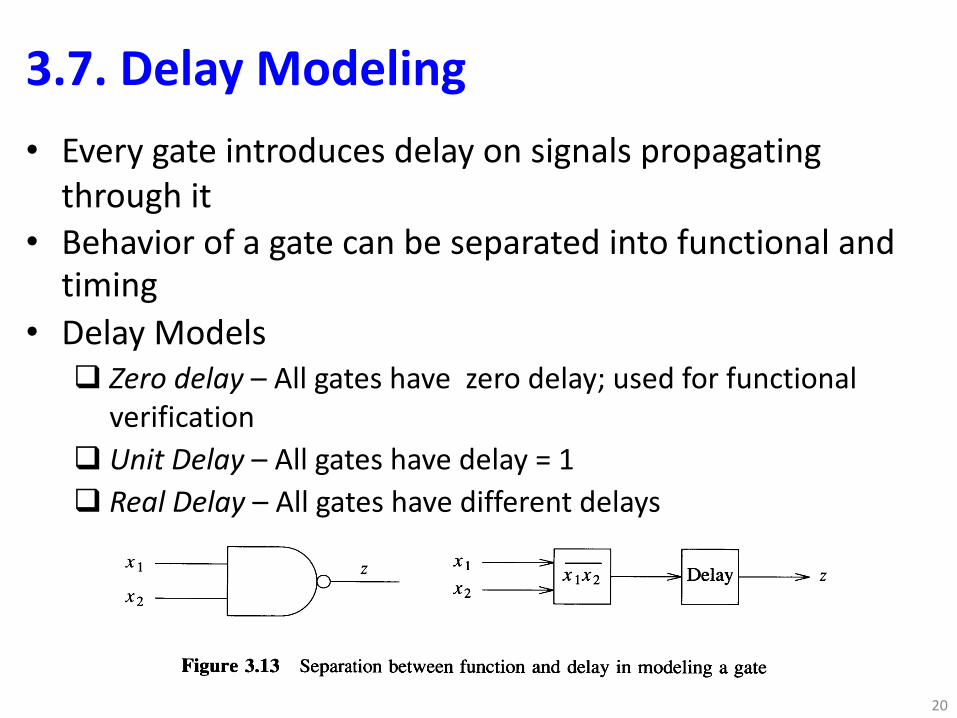
3.7. Delay Modeling
20
• Every gate introduces delay on signals propagating through it
• Behavior of a gate can be separated into functional and timing
• Delay Modelsq Zero delay – All gates have zero delay; used for functional
verificationq Unit Delay – All gates have delay = 1q Real Delay – All gates have different delays
52 LOGIC SIMULATION
• Stop the simulation.
3.7 Delay ModelsMany different variants of the general flow shown in Figure 3.12 exist. Thedifferences among them arise mainly from different delay models associated with thebehavior of the components in the model. Delay modeling is a key element controllingthe trade-off between the accuracy and the complexity of the simulation algorithm.
3.7.1 Delay Modeling for GatesEvery gate introduces a delay to the signals propagating through it. In modeling thebehavior of a gate, we separate its function and its timing as indicated in Figure 3.13.Thus in simulation an activated element is first evaluated, then the delay computationis performed.
zz-----11 )......----Figure 3.13 Separation between function and delay in modeling a gate
Transport Delays
The basic delay model is that of a transport delay, which specifies the interval dseparating an output change from the input change(s) which caused it.
To simplify the simulation algorithm, delay values used in simulation are usuallyintegers. Typically they are multiples of some common unit. For example, if we aredealing with gate delays of 15, 20, and 30 ns, for simulation we can scale themrespectively to 3, 4, and 6 units, where a unit of delay represents the greatest commondivisor (5 ns) of the individual delays. (Then the times of the changes at the primaryinputs should be similarly scaled.) If all transport delays in a circuit are consideredequal, then we can scale them to 1 unit; this model is called a unit-delay model.
The answers to the following two questions determine the nature of the delaycomputation.
• Does the delay depend on the direction of the resulting output transition?
• Are delays precisely known?
For some devices the times required for the output signal to rise (0 to 1 transition*)and to fall (1 to 0) are greatly different. For some MOS devices these delays may
* We assume a positive logic convention, where the logic level 1 represents the highest voltage level.
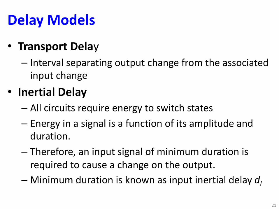
Delay Models• Transport Delay– Interval separating output change from the associated
input change• Inertial Delay– All circuits require energy to switch states– Energy in a signal is a function of its amplitude and
duration.– Therefore, an input signal of minimum duration is
required to cause a change on the output.– Minimum duration is known as input inertial delay dI
21
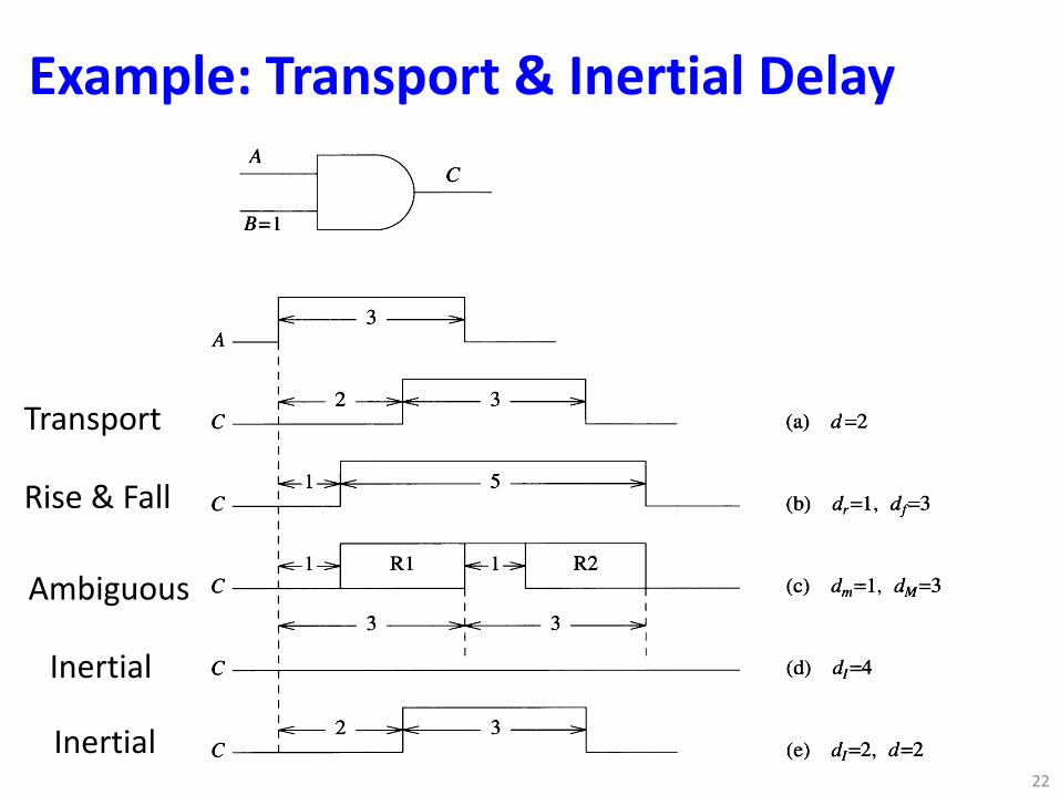
Example: Transport & Inertial Delay
22
Transport
Rise & Fall
Ambiguous
Inertial
Inertial
Delay Models 53
differ by a ratio of 3 to 1. To reflect this phenomenon in simulation, we associatedifferent rise and fall delays, d, and df , with every gate. The delay computationselects the appropriate value based on the event generated for the gate output. If thegate delays are not a function of the direction of the output change, then we can use atransition-independent delay model. Figures 3.14(a) and (b) illustrate the differencesbetween these two models. Note that the result of having different rise and fall delaysis to change the width of the pulse propagating through the gate.
cA
B=1-I
A ---J< 3
II
3c (a) d=2
II
5C (b) dr=l, dj=3I
II
Rl R R2C (c) dm=l, dM=3
II I
I 3 3IEI
I II I
C I (d) d[=4III
3C (e) d[=2, d=2
Figure 3.14 Delay models (a) Nominal transition-independent transport delay(b) Rise and fall delays (c) Ambiguous delay (d) Inertial delay (pulsesuppression) (e) Inertial delay
Often the exact transport delay of a gate is not known. For example, the delay of acertain type of NAND gate may be specified by its manufacturer as varying from 5 nsto 10 ns. To reflect this uncertainty in simulation, we associate an ambiguity interval,defined by the minimum (dm ) and maximum (dM ) delays, with every gate. This model,referred to as an ambiguous delay model, results in intervals (Rl and R2 inFigure 3.14(c)) during which the value of a signal is not precisely known. Under theassumption that the gate delays are known, we have a nominal delay model. The rise
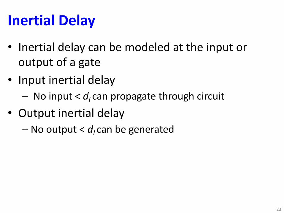
Inertial Delay• Inertial delay can be modeled at the input or
output of a gate• Input inertial delay– No input < dI can propagate through circuit
• Output inertial delay– No output < dI can be generated
23
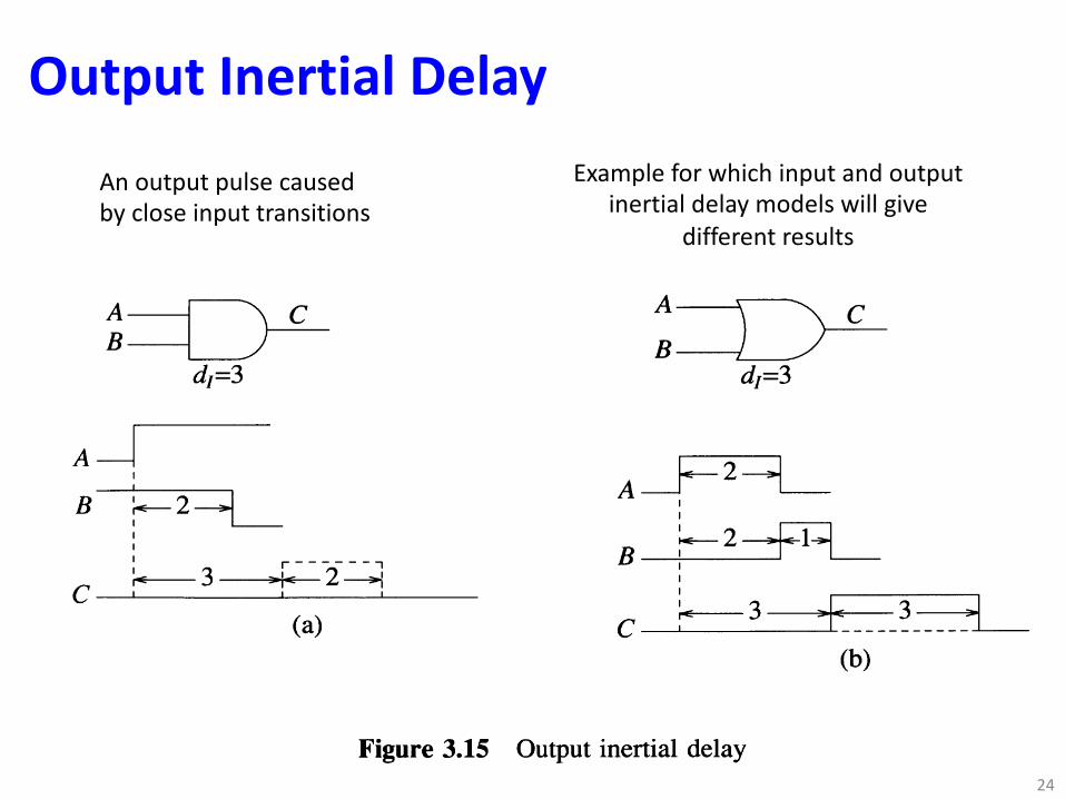
Output Inertial Delay
24
An output pulse causedby close input transitions
Example for which input and outputinertial delay models will give
different results
54 LOGIC SIMULATION
and fall delay model and the ambiguous delay model can be combined such that wehave different ambiguity intervals for the rise (drm, drMl and the fall (dIm' djM) delays[Chappel and Yau 1971].
Inertial Delays
All circuits require energy to switch states. The energy in a signal is a function of itsamplitude and duration. If its duration is too short, the signal will not force the deviceto switch. The minimum duration of an input change necessary for the gate output toswitch states is called the input inertial delay of the gate, denoted by d[. An inputpulse whose duration is less than d[ is said to be a spike, which is filtered (orsuppressed) by the gate (Figure 3.14(d)). If the pulse width is at least d[, then itspropagation through the gate is determined by the transport delay(s) of the gate. If thegate has a transition-independent nominal transport delay d, then the two delays mustsatisfy the relation (Problem 3.6). Figure 3.14(e) shows a case with d[=d.
A slightly different way of modeling inertial delays is to associate them with the gateoutputs. This output inertial delay model specifies that the gate output cannot generatea pulse whose duration is less than d[. An output pulse may be caused by an inputpulse (and hence we get the same results as for the input inertial delay model), but itmay also be caused by "close" input transitions, as shown in Figure 3.15(a). Anothercase in which the two inertial delay models would differ is illustrated inFigure 3.15(b). With the input inertial delay model, the input pulses are consideredseparately and they cannot switch the gate output. However, under the output inertialdelay model, the combined effect of the input pulses forces the output to switch.
(a)
I
I
C(b)
r------.,
, I
III
B
A-JI
C _....L...- .1--__--L- _
Figure 3.15 Output inertial delay
3.7.2 Delay Modeling for Functional ElementsBoth the logic function and the timing characteristics of functional elements are morecomplex than those of the gates. Consider, for example, the behavior of anedge-triggered D F/F with asynchronous set (S) and reset (R), described by the tablegiven in Figure 3.16. The symbol i denotes a 0-to-1 transition. The notation d/lo

Delay Modeling - FF
25
• Delays in FF more complex• Rise, Fall, input-to-output (I/O) delays
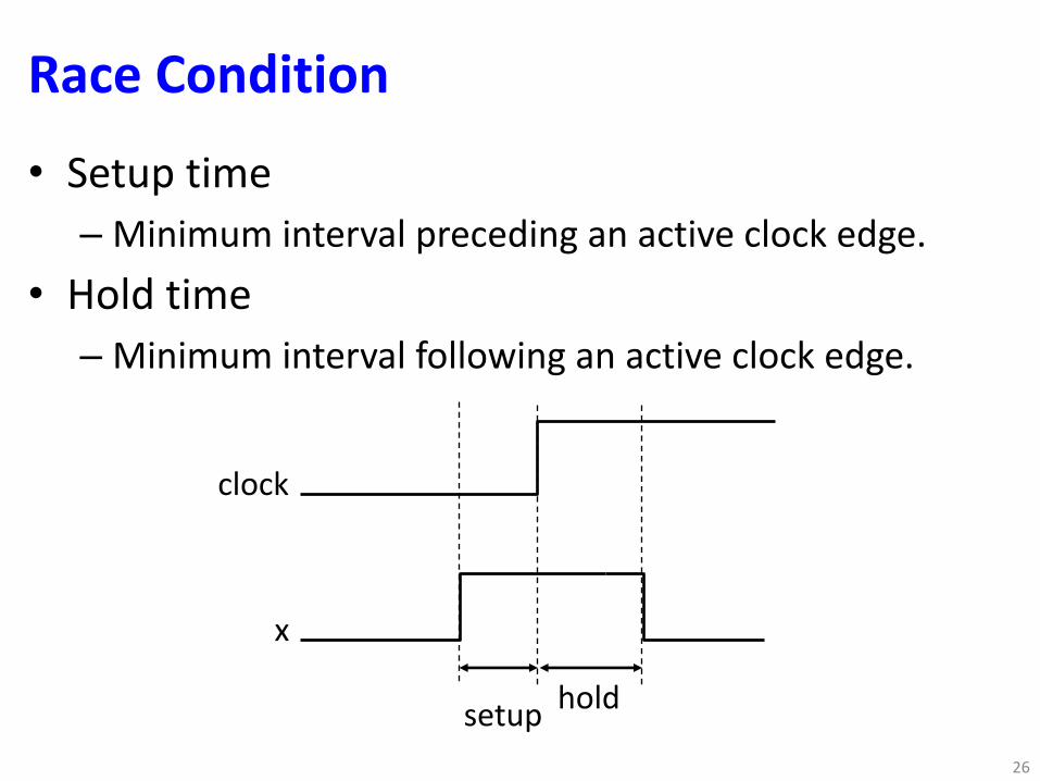
Race Condition• Setup time– Minimum interval preceding an active clock edge.
• Hold time– Minimum interval following an active clock edge.
26
clock
x
setup hold
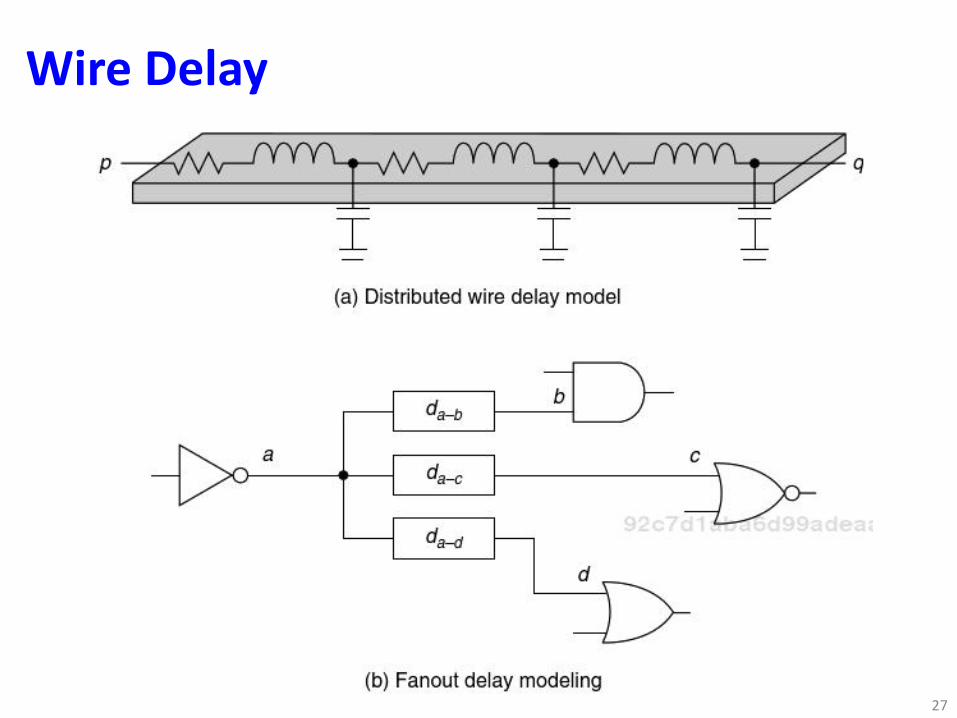
Wire Delay
27
Wang, Laung-Terng, Wu, Cheng-Wen, and Wen, Xiaoqing. Morgan Kaufmann Series in Systems on Silicon : VLSI Test Principles and Architectures : Design for Testability (1). Burlington, US: Morgan Kaufmann, 2006. ProQuest ebrary. Web. 4 January 2017.Copyright © 2006. Morgan Kaufmann. All rights reserved.

3.8 Evaluation of Logic Elements• A process computing output of a logic element
based on its inputs and current state.– Truth table is an obvious choice.– More advanced techniques to speed up simulation:
input scanning, input counting, parallel simulation.
28
Wang, Laung-Terng, Wu, Cheng-Wen, and Wen, Xiaoqing. Morgan Kaufmann Series in Systems on Silicon : VLSI Test Principles and Architectures : Design for Testability (1). Burlington, US: Morgan Kaufmann, 2006. ProQuest ebrary. Web. 4 January 2017.Copyright © 2006. Morgan Kaufmann. All rights reserved.
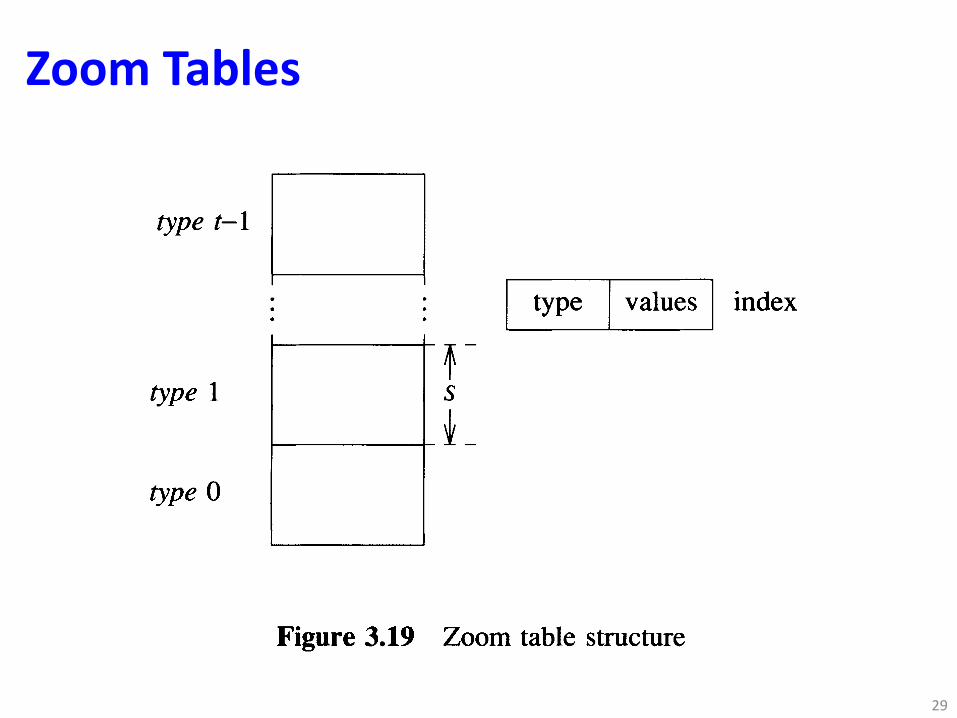
Zoom Tables
29
S8 LOGIC SIMULATION
Evaluation techniques based on truth tables are fast, but because of the exponentialincrease in the amount of memory they require, they are limited to elements thatdepend on a small number of variables.
A trade-off between speed and storage can be achieved by using a one-bit flag in thevalue area of an element to indicate whether any variable has a nonbinary value. If allvalues are binary, then the evaluation is done by accessing the truth table; otherwise aspecial routine is used. This technique requires less memory, since truth tables arenow defined only for binary values. The loss in speed for nonbinary values is notsignificant, because, in general, most of the evaluations done during a simulation runinvolve only binary values.
Zoom Tables
An evaluation technique based on truth tables must first use the type of the evaluatedelement to determine the truth table to access. Thus checking the type and accessingthe truth table are separate steps. These two consecutive steps can be combined into asingle step as follows. Let t be the number of types and let S be the size of the largesttruth table. We build a zoom table of size tS, in which we store the t individual truthtables, starting at locations 0, S, ..., (t-l )S. To evaluate an element, we pack its typecode (in the range 0 to t-l) in the same word with its values, such that we can use thevalue of this word as an index into the zoom table (see Figure 3.19).
typet-l DI type Ivalues I index
type 1
type 0
Figure 3.19 Zoom table structure
This type of zoom table is an instance of a general speed-up technique that reduces asequence of k decisions to a single step. Suppose that every decision step i is based ona variable Xi which can take one of a possible set of m, values. If all Xi'S are knownbeforehand, we can combine them into one cross-product variable Xl x X2 x...x Xk
which can take one of the possible m I m 2 .. .m, values. In this way the k variables areexamined simultaneously and the decision sequence is reduced to one step. Morecomplex zoom tables used for evaluation are described in [Ulrich et al. 1972].
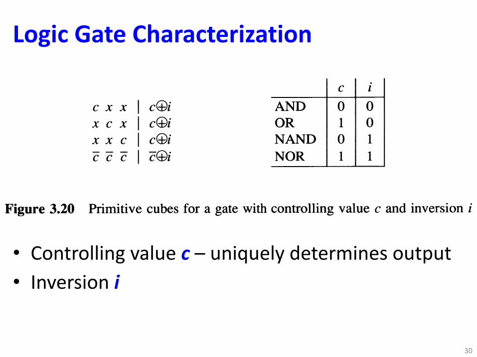
Logic Gate Characterization
• Controlling value c – uniquely determines output• Inversion i
30
Element Evaluation 59
Input Scanning
The set of primitive elements used in most simulation systems includes the basicgates - AND, OR, NAND, and NOR. These gates can be characterized by twoparameters, the controlling value c and the inversion i. The value of an input is saidto be controlling if it determines the value of the gate output regardless of the valuesof the other inputs; then the output value is c(±)i. Figure 3.20 shows the general formof the primitive cubes of any gate with three inputs.
ccxx c(±)i AND 0 0x c x c(±)i OR 1 0x x c c(±)i NAND 0 1c c c c@i NOR 1 1
Figure 3.20 Primitive cubes for a gate with controlling value c and inversion i
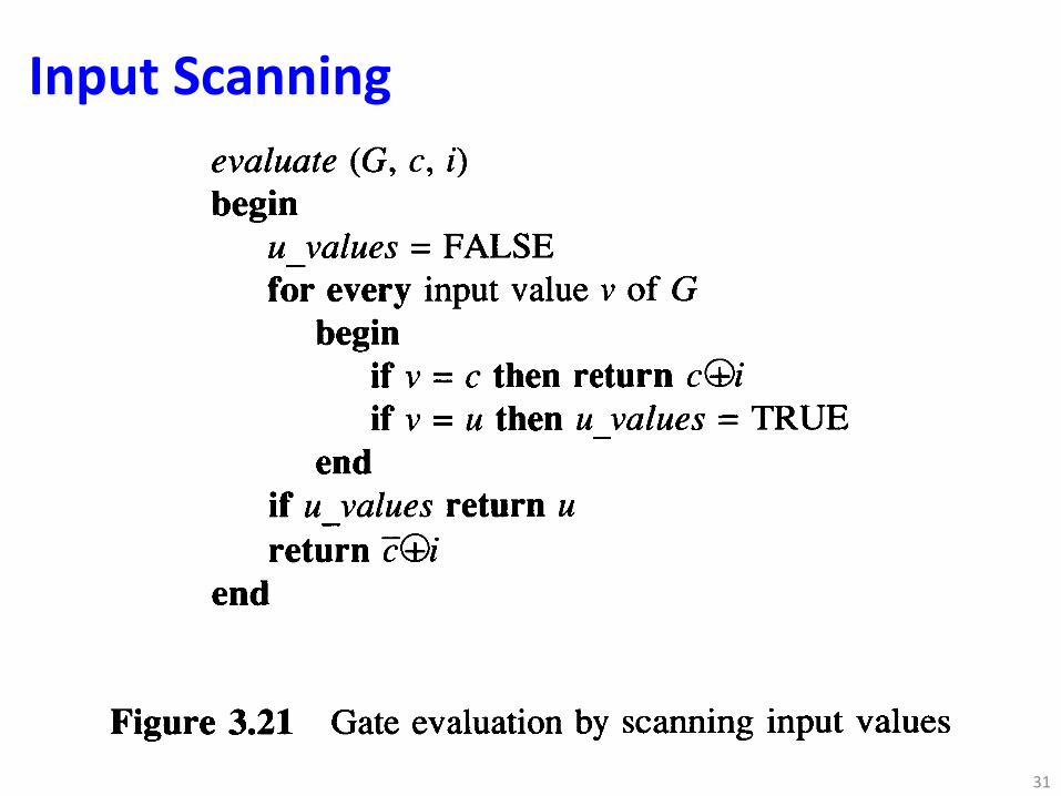
Figure 3.21 outlines a typical gate evaluation routine for 3-valued logic, based onscanning the input values. Note that the scanning is terminated when a controllingvalue is encountered.
evaluate (G, c, i)begin
u values = FALSEfor every input value v of G
beginif v = c then return c@iif v = u then u values = TRUE
endif u values return ureturn c@i
end
Figure 3.21 Gate evaluation by scanning input values
Input Counting
Examining Figure 3.21, we can observe that to evaluate a gate using 3-valued logic, itis sufficient to know whether the gate has any input with c value, and, if not, whetherit has any input with u value. This suggests that, instead of storing the input valuesfor every gate, we can maintain a compressed representation of the values, in the formof two counters - c_count and u_count - which store, respectively, the number ofinputs with c and u values [Schuler 1972]. The step of updating the input values (done
Input Scanning
31
Element Evaluation 59
Input Scanning
The set of primitive elements used in most simulation systems includes the basicgates - AND, OR, NAND, and NOR. These gates can be characterized by twoparameters, the controlling value c and the inversion i. The value of an input is saidto be controlling if it determines the value of the gate output regardless of the valuesof the other inputs; then the output value is c(±)i. Figure 3.20 shows the general formof the primitive cubes of any gate with three inputs.
ccxx c(±)i AND 0 0x c x c(±)i OR 1 0x x c c(±)i NAND 0 1c c c c@i NOR 1 1
Figure 3.20 Primitive cubes for a gate with controlling value c and inversion i
Figure 3.21 outlines a typical gate evaluation routine for 3-valued logic, based onscanning the input values. Note that the scanning is terminated when a controllingvalue is encountered.
evaluate (G, c, i)begin
u values = FALSEfor every input value v of G
beginif v = c then return c@iif v = u then u values = TRUE
endif u values return ureturn c@i
end
Figure 3.21 Gate evaluation by scanning input values
Input Counting
Examining Figure 3.21, we can observe that to evaluate a gate using 3-valued logic, itis sufficient to know whether the gate has any input with c value, and, if not, whetherit has any input with u value. This suggests that, instead of storing the input valuesfor every gate, we can maintain a compressed representation of the values, in the formof two counters - c_count and u_count - which store, respectively, the number ofinputs with c and u values [Schuler 1972]. The step of updating the input values (done
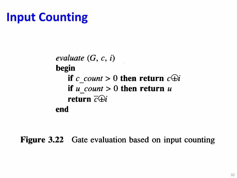
Input Counting
32
60 LOGIC SIMULATION
before evaluation) is now replaced by updating of the two counters. For example, a1 change at an input of an AND gate causes the c_count to be incremented, while a
change results in decrementing the c_count and incrementing the u_count. Theevaluation of a gate involves a simple check of the counters (Figure 3.22). Thistechnique is faster than the input scanning method and is independent of the number ofinputs.
evaluate (G, c, i)begin
if c count> 0 then return c@iif u count > 0 then return ureturn c@i
end
Figure 3.22 Gate evaluation based on input counting
3.9 Hazard DetectionStatic Hazards
In the circuit of Figure 3.23, assume that Q = 1 and A changes from 0 to 1, while Bchanges from 1 to O. If these two changes are such that there exists a short intervalduring which A=B=I, then Z may have a spurious pulse, which may reset thelatch. The possible occurrence of a transient pulse on a signal line whose static valuedoes not change is called a static hazard.
A
B
ZR Q
1 S
Figure 3.23
To detect hazards, a simulator must analyze the transient behavior of signals. Let S(t)and S(t+ 1) be the values of a signal S at two consecutive time units. If these valuesare different, the exact time when S changes in the real circuit is uncertain. To reflectthis uncertainty in simulation, we will introduce a "pseudo time unit" t' between t andt+l during which the value of S is unknown, i.e., Stt') = u [Yoeli and Rinon 1964,Eichelberger 1965]. This is consistent with the meaning of u as one of the values inthe set {O,I}, because during the transition period the value of S can be independently
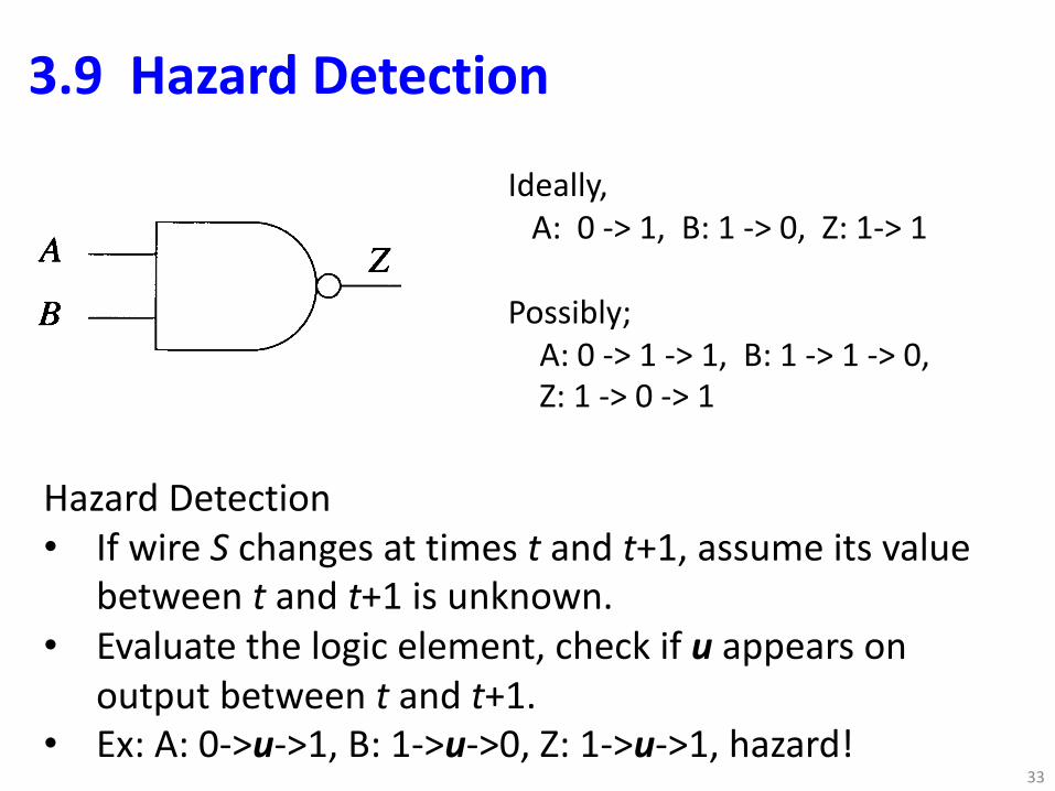
3.9 Hazard Detection
33
Ideally,
A: 0 -> 1, B: 1 -> 0, Z: 1-> 1
Possibly;
A: 0 -> 1 -> 1, B: 1 -> 1 -> 0,
Z: 1 -> 0 -> 1
60 LOGIC SIMULATION
before evaluation) is now replaced by updating of the two counters. For example, a1 change at an input of an AND gate causes the c_count to be incremented, while a
change results in decrementing the c_count and incrementing the u_count. Theevaluation of a gate involves a simple check of the counters (Figure 3.22). Thistechnique is faster than the input scanning method and is independent of the number ofinputs.
evaluate (G, c, i)begin
if c count> 0 then return c@iif u count > 0 then return ureturn c@i
end
Figure 3.22 Gate evaluation based on input counting
3.9 Hazard DetectionStatic Hazards
In the circuit of Figure 3.23, assume that Q = 1 and A changes from 0 to 1, while Bchanges from 1 to O. If these two changes are such that there exists a short intervalduring which A=B=I, then Z may have a spurious pulse, which may reset thelatch. The possible occurrence of a transient pulse on a signal line whose static valuedoes not change is called a static hazard.
A
B
ZR Q
1 S
Figure 3.23
To detect hazards, a simulator must analyze the transient behavior of signals. Let S(t)and S(t+ 1) be the values of a signal S at two consecutive time units. If these valuesare different, the exact time when S changes in the real circuit is uncertain. To reflectthis uncertainty in simulation, we will introduce a "pseudo time unit" t' between t andt+l during which the value of S is unknown, i.e., Stt') = u [Yoeli and Rinon 1964,Eichelberger 1965]. This is consistent with the meaning of u as one of the values inthe set {O,I}, because during the transition period the value of S can be independently
Hazard Detection
• If wire S changes at times t and t+1, assume its value
between t and t+1 is unknown.
• Evaluate the logic element, check if u appears on
output between t and t+1.
• Ex: A: 0->u->1, B: 1->u->0, Z: 1->u->1, hazard!
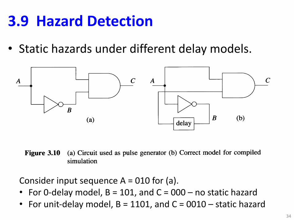
3.9 Hazard Detection• Static hazards under different delay models.
34
Consider input sequence A = 010 for (a).• For 0-delay model, B = 101, and C = 000 – no static hazard• For unit-delay model, B = 1101, and C = 0010 – static hazard
Compiled Simulation 49
y = Y?
Figure 3.9 Asynchronous circuit simulation with compiled-code model
A
(a)
c A
B (b)
c
Figure 3.10 (a) Circuit used as pulse generator (b) Correct model for compiledsimulation
the two vectors cause a critical race, whose result depends on the actual delays in thecircuit. This example shows that a compiled simulator following the procedureoutlined in Figure 3.9, cannot deal with races and hazards which often affect theoperation of an asynchronous circuit. Techniques for detecting hazards will bediscussed in Section 3.9.
3.6 Event-Driven SimulationAn event-driven simulator uses a structural model of a circuit to propagate events. Thechanges in the values of the primary inputs are defined in the stimulus file. Events onthe other lines are produced by the evaluations of the activated elements.
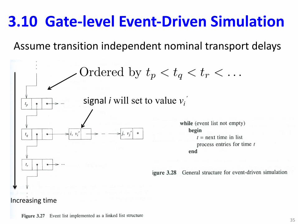
3.10 Gate-level Event-Driven Simulation
35
Assume transition independent nominal transport delays
Increasing time
signal i will set to value vi’
Ordered by tp < tq < tr < . . .
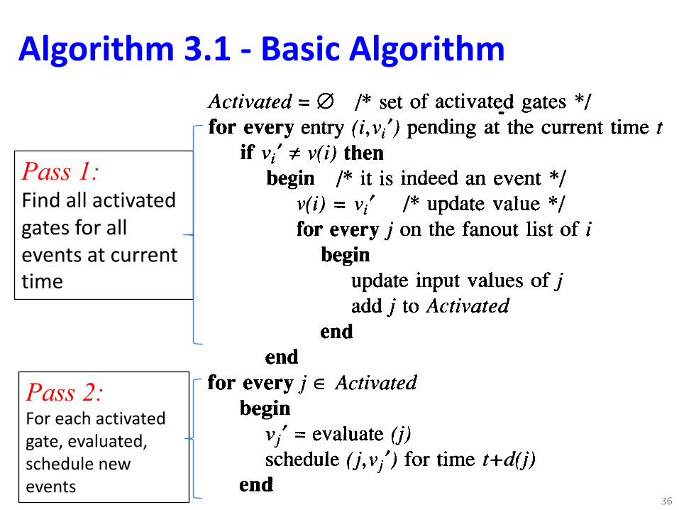
Algorithm 3.1 - Basic Algorithm
36
Pass 1:Find all activated gates for all events at current time
Pass 2:For each activatedgate, evaluated,schedule newevents
66 LOGIC SIMULATION
Activated = 0 /* set of activated gates */for every entry (i.v/') pending at the current time t
if v/ i:- v(i) thenbegin /* it is indeed an event */
v(i) = v/ /* update value */for every j on the fanout list of i
beginupdate input values of jadd j to Activated
endend
for every j E Activatedbegin
Vj' =evaluate (j)schedule (j, Vj') for time t+d(j)
end
Figure 3.29 Algorithm 3.1
and to do the check for activity when the entries are retrieved. For the example inFigure 3.30, (z.O) will be scheduled for time 12 as a result of (a,O) at time 4, but z willalready be set to °at time 10.
z
ba_I 8)"'---
z
Figure 3.30 Example of activation of an already scheduled gate
Algorithm 3.2, given in Figure 3.31, is guaranteed to schedule only true events. Thisis done by comparing the new value Vj', determined by evaluation, with the lastscheduled value of j, denoted by lsv(j). Algorithm 3.2 does fewer schedule operationsthan Algorithm 3.1, but requires more memory and more bookkeeping to maintain thelast scheduled values. To determine which one is more efficient, we have to estimate

Example
37
• Algorithm 3.1 will schedule two (z,0) events at times t=10 and t=12 (wasteful)
• Does not guarantee scheduling of only events
66 LOGIC SIMULATION
Activated = 0 /* set of activated gates */for every entry (i.v/') pending at the current time t
if v/ i:- v(i) thenbegin /* it is indeed an event */
v(i) = v/ /* update value */for every j on the fanout list of i
beginupdate input values of jadd j to Activated
endend
for every j E Activatedbegin
Vj' =evaluate (j)schedule (j, Vj') for time t+d(j)
end
Figure 3.29 Algorithm 3.1
and to do the check for activity when the entries are retrieved. For the example inFigure 3.30, (z.O) will be scheduled for time 12 as a result of (a,O) at time 4, but z willalready be set to °at time 10.
z
ba_I 8)"'---
z
Figure 3.30 Example of activation of an already scheduled gate
Algorithm 3.2, given in Figure 3.31, is guaranteed to schedule only true events. Thisis done by comparing the new value Vj', determined by evaluation, with the lastscheduled value of j, denoted by lsv(j). Algorithm 3.2 does fewer schedule operationsthan Algorithm 3.1, but requires more memory and more bookkeeping to maintain thelast scheduled values. To determine which one is more efficient, we have to estimate
68 LOGIC SIMULATION
items than Algorithm 3.2. Typically the average fanout count! is in the range 1.5 to3. As the event list is a dynamic data structure, these operations involve some form offree-space management. Also scheduling requires finding the proper time slot wherean item should be entered. We can conclude that the cost of the unnecessary event listoperations done by Algorithm 3.1 is greater than that involved in maintaining thelsv values by Algorithm 3.2.
One-Pass Versus Two-Pass Strategy
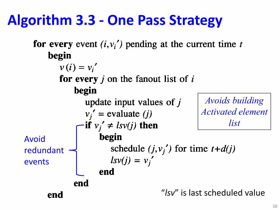
The reason the two-pass strategy performs the evaluations only after all the concurrentevents have been retrieved is to avoid repeated evaluations of gates that have multipleinput changes. Experience shows, however, that most gates are evaluated as a result ofonly one input change. Hence a one-pass strategy [Ulrich 1969], which evaluates agate as soon as it is activated, would be more efficient, since it avoids the overhead ofconstructing the Activated set. Algorithm 3.3, shown in Figure 3.32, implements theone-pass strategy.
for every event (i.v/') pending at the current time tbegin
v(i) = v;'for every j on the fanout list of i
beginupdate input values of jVj' = evaluate (j)if Vj' * lsv(j) then
beginschedule (j, vj') for time t+d(j)lsv(j) = Vj'
endend
end
Figure 3.32 Algorithm 3.3 - one-pass strategy
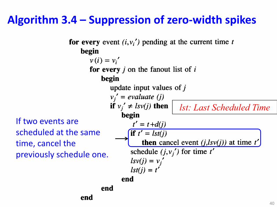
Figure 3.33 illustrates the problem associated with Algorithm 3.3. Inputs a and b arescheduled to change at the same time. If the events are retrieved in the sequence (b,O),(zz.L), then z is never scheduled. But if (a,l) is processed first, this results in (z,l)scheduled for time 4. Next, (b,O) causes (z.O) also to be scheduled for time 4. Henceat time 4, Z will undergo both a O-to-l and a l-to-O transition, which will create azero-width "spike." Although the propagation of this spike may not pose a problem, itis unacceptable to have the results depending on the order of processing of theconcurrent events. Algorithm 3.4, shown in Figure 3.34, overcomes this problem bydetecting the case in which the gate output is repeatedly scheduled for the same timeand by canceling the previously scheduled event. Identifying this situation is helpedby maintaining the last scheduled time, lst(j), for every gate j.
Algorithm 3.3 - One Pass Strategy
38
Avoids buildingActivated element
list
“lsv” is last scheduled value
Avoid redundant events
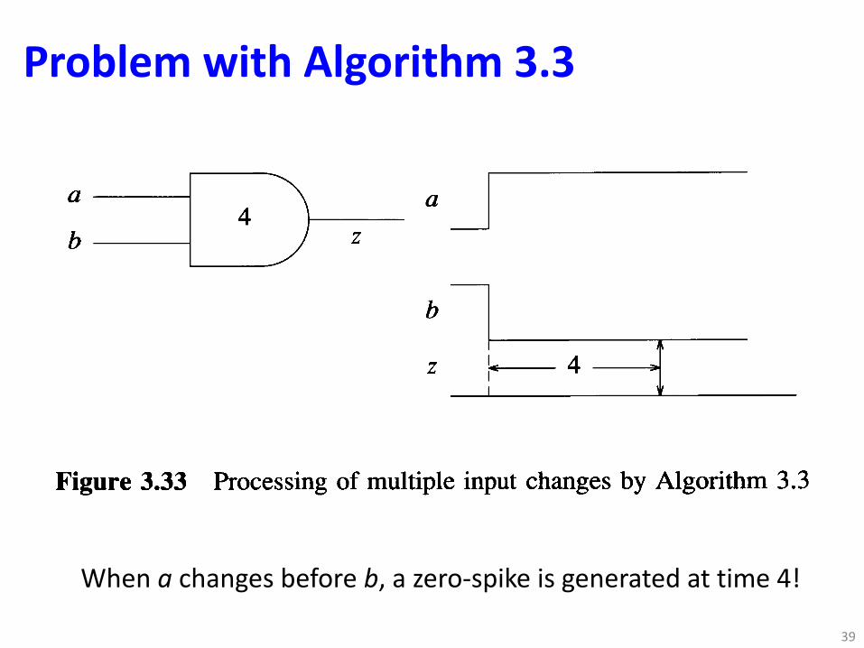
Problem with Algorithm 3.3
39
When a changes before b, a zero-spike is generated at time 4!
Gate-Level Event-Driven Simulation
Figure 3.33 Processing of multiple input changes by Algorithm 3.3
for every event (i.v/') pending at the current time t
beginv(i) = v;'for every j on the fanout list of i
beginupdate input values of jVj' = evaluate (j)if Vj' * lsv(j) then
begint' = t+d(j)
if t' = lst(j)then cancel event (j,lsv(j)) at time t'
schedule (j, Vj') for time t'lsv(j) =Vj'
lst(j) = t'end
endend
Figure 3.34 Algorithm 3.4 - one-pass strategy with suppression of zero-widthspikes
69
Let us check whether with this extra bookkeeping, the one-pass strategy is still moreefficient than the two-pass strategy. The number of insertions in the Activated setperformed during a simulation run by Algorithm 3.2 is about Nf, these are eliminatedin Algorithm 3.4. Algorithm 3.4 performs the check for zero-width spikes only forgates with output events, hence only N times. Canceling a previously scheduled eventis an expensive operation, because it involves a search for the event. However, inmost instances t + d(j) > lst(j), thus event canceling will occur infrequently, and the
Algorithm 3.4 – Suppression of zero-width spikes
40
lst: Last Scheduled TimeIf two events are scheduled at the same time, cancel the previously schedule one.

Gate-Level Event-Driven Simulation 71
3.10.2 Other Logic Values
3.10.2.1 Tristate Logic
Tristate logic allows several devices to time-share a common wire, called a bus. A busconnects the outputs of several bus drivers (see Figure 3.36). Each bus driver iscontrolled by an "enable" signal E. When E=I, the driver is enabled and its output 0takes the value of the input I; when E=O, the driver is disabled and 0 assumes ahigh-impedance state, denoted by an additional logic value Z. O=Z means that theoutput is in effect disconnected from the bus, thus allowing other bus drivers to controlthe bus. In normal operation, at most one driver is enabled at any time. The situationwhen two bus drivers drive the bus to opposite binary values is called a conflict or aclash and may result in physical damage to the devices involved. A pull-up(pull-down) function, realized by connecting the bus to power (ground) via a resistor,provides a "default" 1 (0) logic value on the bus when all the bus drivers are disabled.
E 1
0 1 I
II I
r l -, EI : pull-up orE 2 II I pull-down
O2L1.J if E = 1 then 0 = II
12 if E = ° then 0 = Z
E 3 (b)
13
0 3
(a)
Figure 3.36 (a) Bus (b) bus driver
A bus represents another form of wired logic (see Section 2.4.4) and can be similarlymodeled by a "dummy" component, whose function is given in Figure 3.37. Note thatwhile the value observed on the bus is the forced value computed by the bus function,for every bus driver the simulator should also maintain its own driven value, obtainedby evaluating -the driver. One task of the bus evaluation routine is to report conflictsor potential conflicts to the user, because they usually indicate design errors.Sometimes, it may also be useful to report situations when multiple drivers areenabled, even if their values do not clash. When all the drivers are disabled, theresulting Z value is converted to a binary value if a pull-up or a pull-down is present;otherwise the devices driven by the bus will interpret the Z value as u (assuming lTLtechnology).
Recall that the unknown logic value u represents a value in the set {0,1}. Insimulation, both the input I and the enable signal E of a bus driver can have any of thevalues {O,I,u}. Then what should be the output value of a bus driver with 1=1 andE=u? A case-by-case analysis shows that one needs a new "uncertain" logic value to
Simulating Tri-state Logic
41
• Only one driver should drive the bus•Multiple drivers ® bus conflict (can damage the bus• If all drivers in Z state ® bus is either pulled up or down
Z: High Impedance

Logic Function – Bus
42
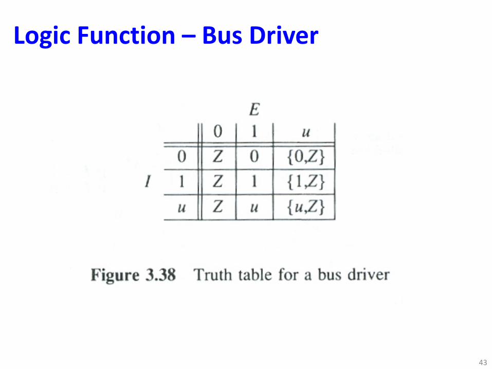
Logic Function – Bus Driver
43
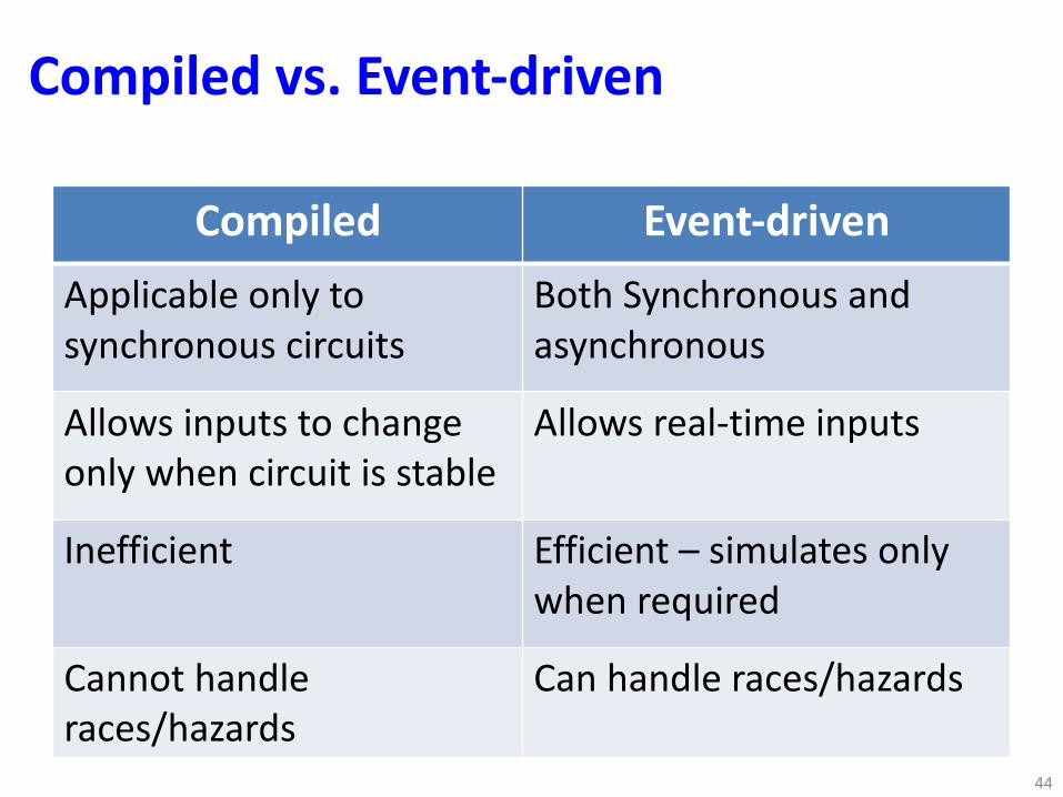
Compiled vs. Event-driven
Compiled Event-drivenApplicable only to synchronous circuits
Both Synchronous and asynchronous
Allows inputs to change only when circuit is stable
Allows real-time inputs
Inefficient Efficient – simulates only when required
Cannot handle races/hazards
Can handle races/hazards
44

Other delay models• We will not consider the following delay models.– Rise & Fall Delay Models• Straightforward extension of Algorithms 3.1-3.4. How?
– Inertial Delay Model– Ambiguous Delays – Oscillation Control
45
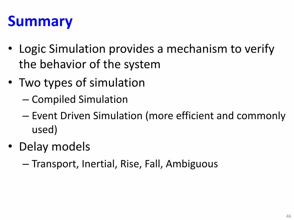
Summary• Logic Simulation provides a mechanism to verify
the behavior of the system• Two types of simulation– Compiled Simulation– Event Driven Simulation (more efficient and commonly
used)• Delay models– Transport, Inertial, Rise, Fall, Ambiguous
46

47
Backup
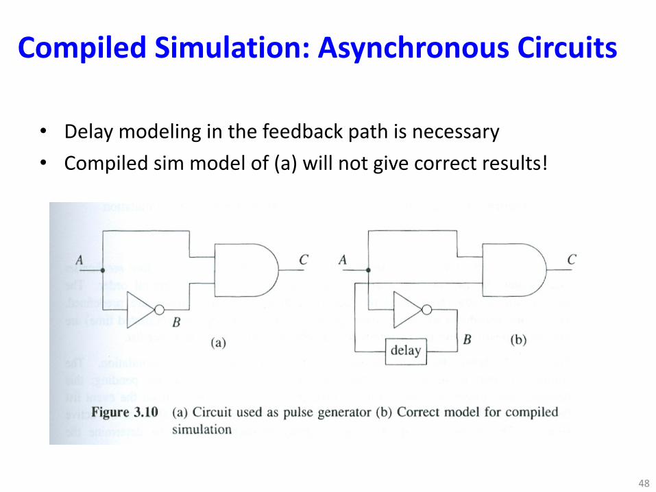
Compiled Simulation: Asynchronous Circuits
48
• Delay modeling in the feedback path is necessary• Compiled sim model of (a) will not give correct results!
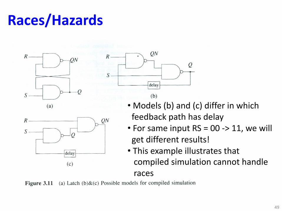
Races/Hazards
49
•Models (b) and (c) differ in whichfeedback path has delay• For same input RS = 00 -> 11, we will get different results!• This example illustrates that
compiled simulation cannot handleraces
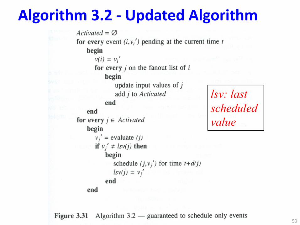
Algorithm 3.2 - Updated Algorithm
50
lsv: last scheduled value