chris stumpf lbmo afm nanolithography report
TRANSCRIPT

AFM Nanolithography of Lanthanum Barium Manganese Oxide (LaBaMnO3) Thin Films: The
Effect of Oxygen Pressure Variations During Film Growth
Christopher Stumpf
Towson University
Abstract
In AFM nanolithography, a bias voltage applied between the tip of an atomic force microscope
(AFM) and a sample is used to produce nanoscale modifications of material surfaces. AFM
nanolithography has been studied extensively on a variety of materials, but limited studies have been
performed on perovskite manganites such as Lanthanum Barium Manganese Oxide (LBMO). Studying
such materials is important because of their potential applications for room-temperature nanoscale
spintronic devices. Previous research on LBMO by our group has focused on how parameters such as
applied tip voltage, temperature, and humidity affect the creation of nanopatterns. This paper reports
on the influence of growth pressure of the LBMO films grown by pulsed laser deposition. Films grown on
(100) SrTiO3 were studied for growth pressures ranging between 100 mTorr to 400 mTorr. Our studies
indicate that the type of nanopatterns induced by AFM and the relaxation dynamics of these patterns
are sensitive to the film growth pressure. The growth pressure is mainly known to affect the oxygen
concentration and the surface roughness, but possible variations in cationic stoichiometry could also
contribute to these results.
Introduction
AFM nanolithography on perovskite manganites is a new research field with important
applications. Perovskite manganites such as lanthanum barium manganese oxide (LBMO) could
potentially be used to create room-temperature nanoscale spintronic devices. Since the field is so new,
there is very little published research on LBMO. The few papers that have been published by Towson
University and Dr. Run-Wei Li have focused on how parameters such as humidity and tip voltage affect
the growth of nanopatterns on the thin film [1].
My research focuses on how the growth pressure of LBMO films grown by pulsed laser
deposition affects the nanopatterns. The growth pressure influences the oxygen concentration and
surface roughness of the LBMO film. I worked with LMBO films grown at 50 mTorr, 100 mTorr, 225
mTorr, and 400 mTorr. I performed nanolithography on each film and compared the results to
determine how growth pressure affects the creation of nanopatterns.
Theory
The science behind AFM nanolithography on perovskite manganites is not completely
understood. For metals and semiconductors, anodic oxidation is the process used to create nanoscale
patterns. In anodic oxidation the sample is placed in a humid environment to allow a water meniscus to
form on the sample’s surface. A voltage bias is then applied between the tip and the sample which
generates an intense electric field around the tip [1]. The electric field ionizes water molecules in the
meniscus to create negatively charged oxygen ions which react with the metal sample to form an oxide
film on the sample’s surface [1].
Anodic oxidation is not the only process behind AFM nanolithography on perovskite oxides.
According to Dr. Run-Wei Li, the reason is that AFM nanolithography can be performed on samples that
do not have many oxygen vacancies [1]. Dr. Li discovered that “oxygen vacancies are not indispensable
for AFM lithography in perovskite oxides. As a result, anodic oxidation should not be the main physical
process of AFM lithography in perovskite oxides. [1]” There may be some anodic oxidation during AFM
nanolithography but it likely only occurs at the sample’s surface [1]. Instead, Dr. Li theorizes that
chemical transport processes such as electromigration and field-induced diffusion might occur during
nanolithography due to the intense electric field between the AFM tip and sample surface [1]. Overall
there are likely several processes at work during AFM nanolithography on perovskite oxides.
Experimental Procedure
Sample Creation
For my research I created four LBMO films under different growth pressures. Each film was
grown on a SrTiO3 (100) substrate by pulsed laser deposition using a krypton fluoride laser. The laser
operated at a wavelength of 248 nm and a frequency of 10 Hz. The substrate was placed inside a
deposition chamber which contained an O2 atmosphere under a growth pressure. I changed the growth
pressure for each sample. During deposition the substrate was heated to 800°C and then hit by 10,000

laser pulses with an energy of 450 mJ. After deposition the newly grown LBMO film was cooled down to
room temperature in an oxygen environment at 500 mTorr with a cooling rate of 20°C per minute. The
only parameter that I changed between the four film depositions was the growth pressure. I created
films with growth pressures of 50 mTorr, 100 mTorr, 225 mTorr, and 400 mTorr. The growth pressure
affects the oxygen concentration and surface roughness of each film. A higher pressure results in a
higher oxygen concentration and a rougher film surface.
Scanning and Writing on the LBMO Films
I performed my nanolithography experiments using a Veeco Multimode V scanning probe
microscope operating in contact mode with silicon tips made by Asylum Research. I used the custom
made LabView program “LC parallel Y lines voltage increments.vi” to write line patterns on the samples.
The program works by moving the AFM tip across the sample’s surface while applying a voltage bias to
the tip. At high humidity, the tip voltage causes an oxide to form on the sample. After it finishes writing
one line the program increments the voltage and moves to a new location to write the next line.
I used the LabView program to create a pattern of 11 lines in a 20 µm scan area. The lines I
created are 16 µm long and are spaced 2 µm apart. I wrote the lines in voltage ranges such as 10V to
20V, 20V to 30V, and -15V to -5V among others. I wrote 11 lines so that I could compare the lines at the
end of the voltage ranges. For example, I compared the height of a 20V line written last in the 10V to
20V range with the height of a 20V line written first in the 20V to 30V range. I wanted to see if the order
of writing affected the line’s height.
All of my line patterns were created at a temperature of roughly 70 °F and a humidity level
between 60% and 75%. I used an AFM writing speed of 1.6 µm/s. I created multiple line patterns for
each voltage range. I then used Nanoscope to measure the height and width of each line in the pattern. I
averaged together the results from each pattern to determine the average height and width of the line
that each applied voltage produced. I also measured the standard deviation of the line heights. My goal
was to determine how well the nanolithography process could be controlled. I also wanted to see if the
line patterns could be easily reproduced. I have included an example data table on the last page.
Growth Pressure and Surface Roughness
The growth pressure has a major impact on the sample’s surface roughness. Samples that are
grown at high growth pressures such as 400 mTorr are rougher than samples grown at low pressures
like 50 mTorr. Sample LBMO-STO-34 was created at the lowest growth pressure of 50 mTorr while
sample LBMO-STO-37 was grown at the highest pressure of 400 mTorr. Sample LBMO-STO-39 was
created at 225 mTorr and sample LBMO-STO- 43 was grown at 100 mTorr. (I will refer to each sample by
its number. I will also list the growth pressure in parentheses after the sample name for clarity.)
Figure 1 consists of four AFM height images that show the surface roughness of each sample.
Each example image is a good representation of the roughness of the whole sample. Figure 1 shows that
a high growth pressure will result in a rougher sample surface. The differences in surface roughness can
also be seen numerically. I used Nanoscope’s roughness command to calculate the average roughness

(Ra) of each sample. The average roughness of sample 34 (50 mTorr) was 0.442 nm while the average
roughness of sample 43 (100 mTorr) was 0.973 nm. For the higher growth pressures, the average
roughness was 2.056 nm for sample 39 (225 mTorr) and 1.356 nm for sample 37 (400 mTorr). High grow
pressures cause large dots to appear on the sample’s surface. Most of the dots are less than 10 nm in
height but a few dots can be 40 nm or more. The dots can make writing difficult but nanolithography is
still possible on high growth pressure samples.
Figure 1: Example images showing the surface roughness for each growth pressure
(a) 50 mTorr surface (sample 34) (b) 100 mTorr surface (sample 43)
(c) 225 mTorr surface (sample 39) (d) 400 mTorr surface (sample 37)
Results
50 mTorr sample, LBMO-STO-34 Sample LBMO-STO-34 was created on May 3, 2013 with a growth pressure of 50 mTorr. The sample has
a very smooth surface which made it easy to write upon. There are few defects on the sample’s surface.
Positive Applied Tip Voltages on Sample 34 (50 mTorr)
I applied positive tip voltages between 1V and 30V to sample 34 (50 mTorr) in order to create
line patterns. I used the LabView program to write either 11 lines in a 20 µm area or 21 lines in a 32 µm
area. I created line patterns in the following voltage ranges: 1V to 10V, 1V to 20V, 5V to 15V, 5V to 25V,
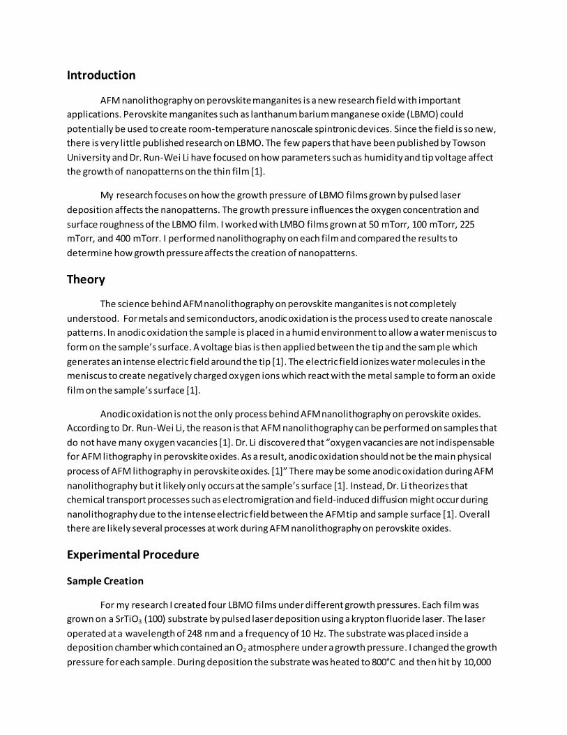
10V to 20V, 15V to 25V, 20V to 30V, and 10V to 30V. Figure 2 shows three examples of positive voltage
line patterns on sample 34 (50 mTorr). The lowest voltage line is the leftmost line in the images. Each
subsequent line was written at 1V larger than the previous line.
Figure 2: Example images of positive voltage line patterns on sample 34
(a) 10V to 20V line pattern (b) 10V to 30V line pattern (c) 10V to 30V line pattern
The quality of the lines produced by positive tip voltages can vary greatly depending on the
humidity. Figure 2 (a) and (b) show clean, well defined lines while image (c) shows a blurry, jagged line
pattern. Images (a) and (b) were created at 73% humidity while image (c) was created at 80% humidity.
A small increase in the humidity can cause the lines to grow uncontrollably.
I performed dozens of positive tip voltage tests on sample 34 (50 mTorr). After writing, I used
the step function in Nanoscope to measure the height and width of each line. I averaged the results
together to determine the average height of the line each voltage produces. I did this in order to see
how controllable the writing process is and if the results are reproducible. Figure 3 on the next page is a
graph of positive tip voltages versus the average line height of voltage. The vertical error bars are the
standard deviations of the line heights. I calculated the standard deviations with the STDEV function in
Microsoft Excel.
As seen in Figure 3, the average line height increases linearly with the voltage. The smallest line
height was 0.184 nm at 5V while the largest height was 27.1 nm at 30V. High voltages will produce
larger lines than small voltages. However a given voltage can produce lines with widely varying heights.
For example, in my tests a 15V applied tip voltage produced lines with heights of 3.73 nm, 7.36 nm, and
13.2 nm among others. As seen in Figure 3, the standard deviation is very large for most of the positive
applied tip voltages. The 5V line has the lowest standard deviation of 0.3825 nm while the 19V line has
the highest deviation of 4.361 nm. The standard deviations for sample 34 (50 mTorr) are higher than the
standard deviations of the other LBMO samples that I will discuss later.
Figure 3 shows that lines do not appear unless a voltage of at least 5V is applied to the AFM tip.
Applied voltages smaller than 5V do not create any growths on the sample. The minimum voltage at
which lines are formed on the sample is called the threshold voltage. 5V is the threshold voltage for
sample 34 (50 mTorr). In his work on LBMO, Dr. Run-Wei Li found that there was also a voltage at which
the lines would not get larger even if higher voltages were applied to the tip. He called this the
10 V 10 V 10 V 30 V 30 V 20 V

saturation point. My data shows that the 50 mTorr sample 34 does not have a saturation point because
the line heights keep increasing as the voltage increases. Other samples that I will discuss later do have
saturation points.
Figure 3: Positive tip voltage vs. average line height with standard deviation bars
In addition to the heights, I also measured each line’s width. Figure 4 shows the average line width
produced by each voltage. Unlike the heights, the line widths have a saturation point.
Figure 4: Positive tip voltages vs. average line width with standard deviation bars
The average line widths ranged from 0.755 µm to 0.976 µm. The smallest line width was 0.461 µm while
the largest width was 1.213 µm. Applying very large voltages only made the lines taller, not wider.
I created line patterns with 11 or 21 lines because I wanted to see if the order in which the lines
are written affects their height. A line could be written first, last, or in the middle of a voltage range. On
sample 34 (50 mTorr), the writing order can influence the line’s height. My data for the 20V line is a
0
5
10
15
20
0 5 10 15 20 25 30Ave
rage
Lin
e H
eig
ht (
nm
)
Voltage (V)
LBMO-STO-34 (50 mTorr) Positive Tip Voltage vs. Average Line Height
0
0.2
0.4
0.6
0.8
1
1.2
1.4
0 5 10 15 20 25 30
Ave
rage
Lin
e W
idth
(µm
)
Voltage (V)
LBMO-STO-34 (50 mTorr) Positive Tip Voltage vs. Average Line Width
good example of the behavior. The 20V line was written last in the 10V to 20V line patterns and first in
the 20V to 30V patterns. It was written in the middle of the pattern in the 10V to 30V range. Table 1
below shows the height of 20V lines written at different points in the writing process.
Table 1: 20V line data on sample 34
Order Written Line Heights (nm) Average line height in bold (nm)
20V line written first (20V to 30V) 4.61 2.48 3.73 6.62 1.97 8.34 4.11 4.55
20V line written in the middle (10V to 30V) 5.18 10.4 6.46 6.68 8.66 5.43 5.65 6.92
20V line written last (10V to 20V) 13.7 14.4 10.6 17.3 9.42 10.1 12.6 12.6
As Table 1 shows, the writing order affects the height of the created line on sample 34 (50 mTorr). The
20V line is not unique; other positive tip voltages produced similar results on sample 34. However, this
behavior did not occur on samples 37, 39, and 43 which all have higher growth pressures. It may be
unique to the 50 mTorr growth pressure.
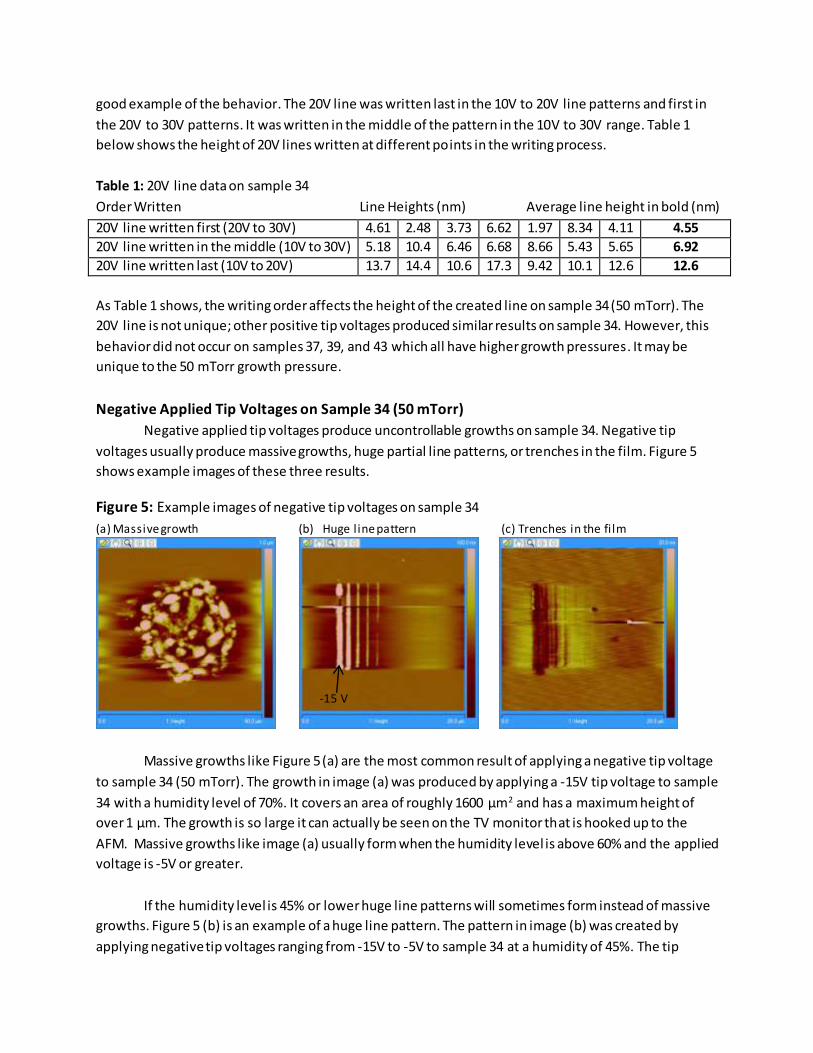
Negative Applied Tip Voltages on Sample 34 (50 mTorr)
Negative applied tip voltages produce uncontrollable growths on sample 34. Negative tip
voltages usually produce massive growths, huge partial line patterns, or trenches in the film. Figure 5
shows example images of these three results.
Figure 5: Example images of negative tip voltages on sample 34
(a) Massive growth (b) Huge line pattern (c) Trenches in the fi lm
Massive growths like Figure 5 (a) are the most common result of applying a negative tip voltage
to sample 34 (50 mTorr). The growth in image (a) was produced by applying a -15V tip voltage to sample
34 with a humidity level of 70%. It covers an area of roughly 1600 µm2 and has a maximum height of
over 1 µm. The growth is so large it can actually be seen on the TV monitor that is hooked up to the
AFM. Massive growths like image (a) usually form when the humidity level is above 60% and the applied
voltage is -5V or greater.
If the humidity level is 45% or lower huge line patterns will sometimes form instead of massive
growths. Figure 5 (b) is an example of a huge line pattern. The pattern in image (b) was created by
applying negative tip voltages ranging from -15V to -5V to sample 34 at a humidity of 45%. The tip
-15 V

writing speed was 1.6 µm/s. The lines in image (b) are very large compared to the positive voltage lines.
The -15V line in image (b) is 123 nm tall while the other lines range from 98 nm to 30 nm in height. The
huge lines do not always appear when the humidity is lower. Sometimes massive growths occur even
when the humidity is less than 45%. Negative voltages produce uncontrollable results.
In rare occasions, trenches will sometimes form on the LBMO film instead of massive growths or
huge lines. Figure 5 (c) is an example of a trench in the film. Image (c) was created by applying voltages
ranging from -20V to -10V to sample 34 at a humidity level of 70%. The created trenches are roughly 10
nm deep. Trenches are much rarer than growths or huge line patterns. I have only had two trenches
form on sample 34 while conducting dozens of negative voltage tests
Finally, applying a small negative voltage to sample 34 at a low humidity will produce no
reaction at all. I applied a -5V tip voltage to sample 34 at a humidity of 40%. No reaction occurred during
this test. No growths formed and the sample was unchanged. There is a threshold voltage of
approximately -5V for negative voltages on sample 34. Voltages lower than -5V do not produce growths
even if the humidity is very high.
Pattern Relaxation and Surface Aging on Sample 34 (50 mTorr)
In his work on LBMO, Dr. Run-Wei Li discovered that the line patterns would shrink and
disappear after a certain period of time. He called this phenomenon relaxation. I performed tests on all
four of my LBMO samples to see if they also experienced relaxation. In my tests, I wrote a line pattern
on a Friday afternoon and then left the sample in the AFM for approximately 72 hours before rescanning
the pattern. I also performed tests to see how the surface of the sample changed with age. The LBMO
samples tend to become rougher as they age.
I discovered that sample 34 does not experience any relaxation. Instead the line patterns
seemed to slightly grow over the 72 hour period. I also discovered that aging has made sample 34 more
difficult to write on. I tried to write a 10V to 20V line pattern on sample 34 in May 2014, one year after
the sample was created. The patterned that I created was much fainter than patterns I created in May
2013. I used the sample parameters and tips at both times.
Sample 34 (50 mTorr) Conclusions
Positive voltages produce clear and well defined lines on sample 34. We could use the positive
tip voltages to create advanced nanolithography patterns on 50 mTorr LBMO samples. Negative tip
voltages produce random growths and patterns. The negative voltages are too uncontrollable to use in
advanced nanolithography.
400 mTorr sample, LBMO-STO-37 Sample LBMO-STO-37 was created on September 7, 2013 with a growth pressure of 400 mTorr.
The high growth pressure made sample 37’s surface much rougher than sample 34’s surface. Despite
the rough surface, AFM nanolithography can still be performed on sample 37. In fact, both positive and
negative tip voltages produce line patterns on sample 37.
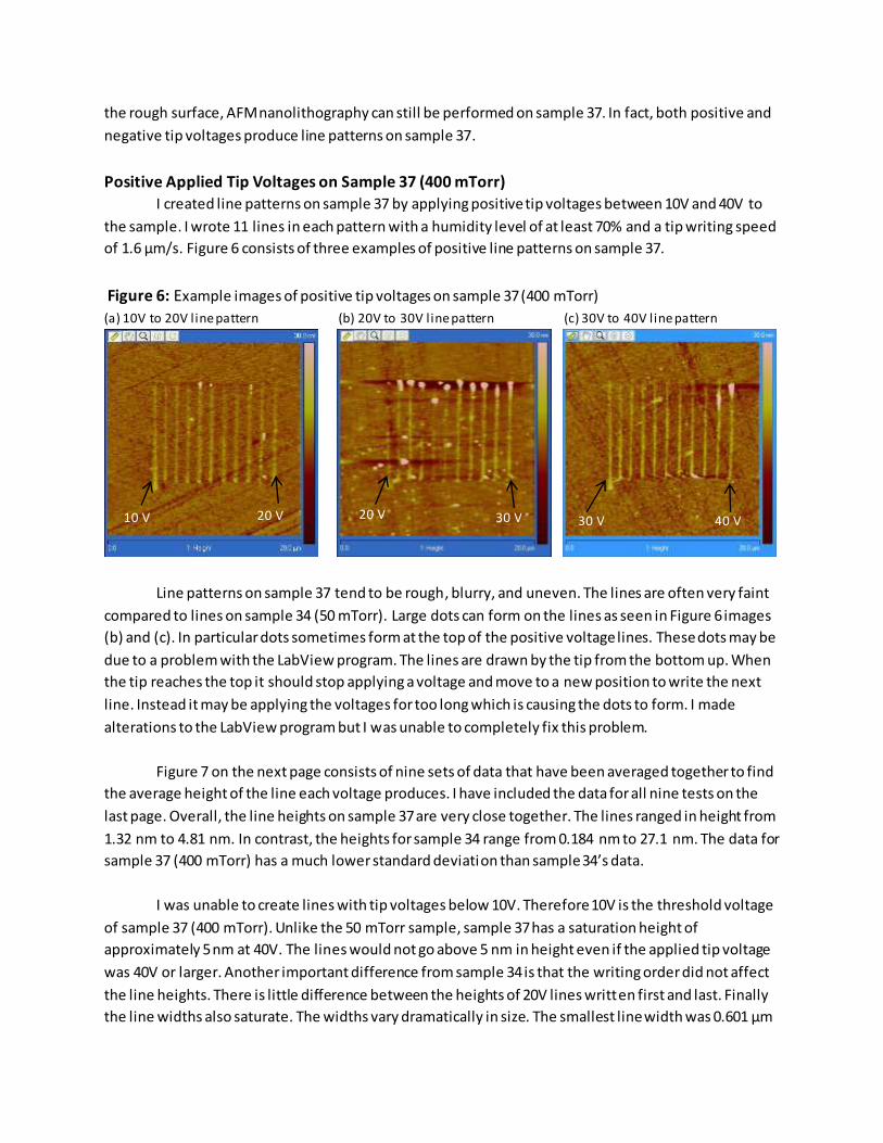
Positive Applied Tip Voltages on Sample 37 (400 mTorr) I created line patterns on sample 37 by applying positive tip voltages between 10V and 40V to
the sample. I wrote 11 lines in each pattern with a humidity level of at least 70% and a tip writing speed
of 1.6 µm/s. Figure 6 consists of three examples of positive line patterns on sample 37.
Figure 6: Example images of positive tip voltages on sample 37 (400 mTorr)
(a) 10V to 20V line pattern (b) 20V to 30V line pattern (c) 30V to 40V line pattern
Line patterns on sample 37 tend to be rough, blurry, and uneven. The lines are often very faint
compared to lines on sample 34 (50 mTorr). Large dots can form on the lines as seen in Figure 6 images
(b) and (c). In particular dots sometimes form at the top of the positive voltage lines. These dots may be
due to a problem with the LabView program. The lines are drawn by the tip from the bottom up. When
the tip reaches the top it should stop applying a voltage and move to a new position to write the next
line. Instead it may be applying the voltages for too long which is causing the dots to form. I made
alterations to the LabView program but I was unable to completely fix this problem.
Figure 7 on the next page consists of nine sets of data that have been averaged together to find
the average height of the line each voltage produces. I have included the data for all nine tests on the
last page. Overall, the line heights on sample 37 are very close together. The lines ranged in height from
1.32 nm to 4.81 nm. In contrast, the heights for sample 34 range from 0.184 nm to 27.1 nm. The data for
sample 37 (400 mTorr) has a much lower standard deviation than sample 34’s data.
I was unable to create lines with tip voltages below 10V. Therefore 10V is the threshold voltage
of sample 37 (400 mTorr). Unlike the 50 mTorr sample, sample 37 has a saturation height of
approximately 5 nm at 40V. The lines would not go above 5 nm in height even if the applied tip voltage
was 40V or larger. Another important difference from sample 34 is that the writing order did not affect
the line heights. There is little difference between the heights of 20V lines written first and last. Finally
the line widths also saturate. The widths vary dramatically in size. The smallest line width was 0.601 µm
10 V 20 V 20 V 30 V 40 V 30 V
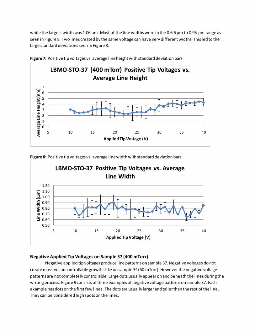
while the largest width was 1.06 µm. Most of the line widths were in the 0.6.5 µm to 0.95 µm range as
seen in Figure 8. Two lines created by the same voltage can have very different widths. This led to the
large standard deviations seen in Figure 8.
Figure 7: Positive tip voltages vs. average line height with standard deviation bars
Figure 8: Positive tip voltages vs. average line width with standard deviation bars
Negative Applied Tip Voltages on Sample 37 (400 mTorr)
Negative applied tip voltages produce line patterns on sample 37. Negative voltages do not
create massive, uncontrollable growths like on sample 34 (50 mTorr). However the negative voltage
patterns are not completely controllable. Large dots usually appear on and beneath the lines during the
writing process. Figure 9 consists of three examples of negative voltage patterns on sample 37. Each
example has dots on the first few lines. The dots are usually larger and taller than the rest of the line.
They can be considered high spots on the lines.
0
1
2
3
4
5
6
7
5 10 15 20 25 30 35 40
Ave
rage
Lin
e H
eig
ht (
nm
)
Applied Tip Voltage (V)
LBMO-STO-37 (400 mTorr) Positive Tip Voltages vs. Average Line Height
0.50
0.60
0.70
0.80
0.90
1.00
1.10
1.20
5 10 15 20 25 30 35 40
Lin
e W
idth
(µm
)
Applied Tip Voltage (V)
LBMO-STO-37 Positive Tip Voltages vs. Average Line Width

Figure 9: Example images of negative tip voltages on sample 37 (400 mTorr) with dots on the lines
(a) -30V to -20V line pattern (b) -25V to -15V line pattern (c) -25V to -15V line pattern
I wrote negative patterns in the following voltage ranges: -30V to -20V, -25V to -15V, and -20V
to -10V. Like the positive voltages, I wrote 11 lines in each negative voltage pattern with a humidity level
of at least 70% and a tip writing speed of 1.6 µm/s. The negative lines are fainter and rougher than the
positive voltage lines on sample 37. The lines often have large dots on the first few lines along with dots
at the bottom. Like the dots on the positive voltage lines, the growths at the bottom of the negative
lines are likely caused by a problem with the LabView program. The tip is likely applying a voltage at the
bottom for too long which causes large growths. Unfortunately, I was unable to fix this problem.
The dots on the actual lines are more random than the dots at the bottom. As seen in Figure 9,
the dots usually only form on the first three or four lines drawn. The remaining lines do not have dots
although they can be very faint. In Figure 9 (a) the dots are only on the -30V, -29V and -28V lines. In
image (b) the dots are on the -25V and -24V lines and in (c) the dots are on the -25V to -23V lines. The -
25V lines in images (b) and (c) have dots on them. However the -25V line in image (a) does not have any
dots on it. The -25V line in image (a) was written in the middle of the writing test instead of at the
beginning like in (b) and (c). This suggests that the writing order can determine where the dots appear
on the lines. This is similar to how writing order affected the line heights for posi tive voltages on sample
34.
Figure 10 on the next page shows the average line height for each applied negative voltage on
sample 37 (400 mTorr). The dots on the lines are included in the line height measurements. The dots
increased the height of the -30V, -29V and -28V lines. Their increased height can be seen on the left part
of the Figure 10 graph. The -27V and -26V lines in image (a) did not have any dots on them so their
height is lower than the -30V to -28V lines. As shown in Figure 9 (b) and (c) the -25V to -23V lines also
had many dots on them. The dots increased the line heights of those three lines which can be seen on
the graph. The dots increased the line height by various amounts which lead to large standard
deviations for the -25V and -24V lines. The standard deviations are 5.50 nm for the -25V line and 5.72
nm for the -24V line.
-30 V -20 V -15 V -15V
-25V -25V
-25 V

The -22V to -10V lines have no dots on them and follow a slightly linear relationship. The line
heights slowly increased as the voltage became more negative. For negative voltages, sample 37 (400
mTorr) has a threshold voltage of -10V. Due to the presence of the dots on the lines, I cannot determine
if sample 37 has a saturation voltage and height. I was able to measure the line widths which are shown
in Figure 11. Even with the dots, most lines were roughly 0.7 µm wide.
Figure 10: Negative tip voltages vs. average line height with standard deviation bars
Figure 11: Negative tip voltages vs. average line width with standard deviation bars
Pattern Relaxation and Surface Aging on Sample 37 (400 mTorr)
I performed relaxation tests on both positive and negative line patterns on sample 37. After 72
hours, both the positive and negative patterns had slightly grown. The growth for each line was less than
half a nanometer. Sample 37 was made in September 2013. In May 2014 I attempted to write positive
and negative patterns on the sample. I was able to write a positive line pattern but I was completely
unable to write a negative voltage pattern. The positive line pattern that I was able to write was fainter
0
5
10
15
20
-30 -28 -26 -24 -22 -20 -18 -16 -14 -12 -10Ave
rage
Lin
e H
eig
ht (
nm
)
Voltage (V)
LBMO-STO-37 Negative Tip Voltages vs. Average Line Height
0
0.2
0.4
0.6
0.8
1
-30 -28 -26 -24 -22 -20 -18 -16 -14 -12 -10Ave
rage
Lin
e W
idth
(µm
)
Voltage (V)
LBMO-STO-37 Negative Voltages vs. Average Line Width

than patterns I wrote back in September 2013. Sample 37’s age affected the ability to write patterns on
it.
Sample 37 (400 mTorr) Conclusions
Although the sample’s surface is rough, positive tip voltages produce controllable and
reproducible line patterns on sample 37. If the dots at the top of the lines can be removed sample 37
could be used for more advanced nanolithography projects. The lines produced by negative tip voltages
are difficult to control and have many dots on them. Although they do produce lines, negative tip
voltages are too random to be used for nanolithography on 400 mTorr samples.
225 mTorr sample, LBMO-STO-39 Sample LBMO-STO-39 was created in November, 2013 with a growth pressure of 225 mTorr. I
decided to use a 225 mTorr growth pressure because it is exactly in between the 50 mTorr and 400
mTorr pressures of samples 34 and 37 respectively. Sample 39 is covered in small dots and growths.
There are no clean areas on the film so I had to write the line patterns on top of the dots. I was able to
write some lines with both positive and negative voltages.
Positive Applied Tip Voltages on Sample 39 (225 mTorr)
I wrote positive tip voltage line patterns on sample 39 in the following voltage ranges: 10V to
20V, 15V to 25V, 20V to 30V, and 25V to 35V. Like the previous samples, I wrote 11 lines with a 70%
humidity and a 1.6 µm/s writing speed. Figure 12 shows three positive voltage line patterns on sample
39 along with the many dots on the sample.
Figure 12: Example images of positive tip voltage line patterns on sample 39 (225 mTorr)
(a) 10V to 20V line pattern (b) 20V to 30V line pattern (c) 25V to 35V line pattern
10 V 20 V 30 V 20 V 25 V 35 V

(d) 25V to 35V line pattern
The drawn lines can vary dramatically in height and width. As
seen in Figure 12, two lines right next to each other can have
dramatically different heights and widths. The lines in the middle of
images (b) and (c) are much smaller than the lines on the left and right
sides of the images. The difference in size may be caused by the many
dots on the sample’s surface. Since there are so many dots, I had to
write over them when creating the line patterns. In images (a), (b), and
(c) there are large dots right next to the faint lines. The dots likely
affected the ability of the tip to drawn clean lines. Images (c) and (d)
both show 25V to 35V line patterns. However the surface of image (d) is much cleaner than image (c) ’s
surface. The tip was able to create a better line pattern on image (d) because of its cleaner surface.
The heights and widths of the lines can greatly vary due to the dots on the sample. I averaged
together the varying heights and plotted them versus applied tip voltage in Figure 13.
Figure 13: Positive tip voltages vs. average line height with standard deviation bars
The most important feature of Figure 13 is the large standard deviation bars. The dots on the
sample caused a large spread in my data which can be seen in the bars. The highest standard deviation
was 4.54 nm at the 27V line. The largest voltage line that I measured was 13.8 nm tall at the 27V line.
The smallest voltage line was 0.735 nm tall at the 25V line. The 13.8 nm at 27V line appears to be the
positive voltage saturation height and voltage of sample 39. Like sample 37, sample 39 (225 mTorr) has
a threshold voltage of 10V.
The positive voltage lines have a maximum width of 1.171 µm at 30V. The smallest width is
0.323 µm at the 11V line. Most of the line widths are between 0.4 µm and 0.9 µm. The largest standard
deviation is 0.224 µm at 10V.
0
2
4
6
8
10
12
5 10 15 20 25 30 35Ave
rage
Lin
e H
eig
ht (
nm
)
Voltage (V)
LBMO-STO-39 Positive Tip Voltages vs. Average Line Height
25 V 35 V

Figure 14: Positive tip voltages vs. average line width for sample 39 with standard deviation bars.
Negative Applied Tip Voltages on Sample 39 (225 mTorr) For negative lines I used the same writing parameters as the positive voltage lines. I wrote 11
lines in each pattern in voltages ranges including: -35V to -25V, -30V to -20V, -25V to -15V, and -20V to -
10V. Unlike the positive voltages, the negative voltages did not create all 11 lines. As shown in figure 15,
many of the lines are missing or are only partially written. Some lines seem to be skipped over by the
tip. The dots on the sample’s surface affect the height and width of the lines that are drawn.
Figure 15: Example images of negative tip voltages line patterns on sample 39 (225 mTorr)
(a) -20V to -10V line pattern (b) -30V to -20V line pattern (c) -35V to -25V line pattern
As seen in the previous section, positive tip voltages produced all 11 lines even though the lines
could be very faint and small. There is likely some reaction that occurs only with negative voltages and
prevents the lines from being drawn. Although many lines are missing I measured the height and width
of all the lines that were written.
0
0.2
0.4
0.6
0.8
1
1.2
5 10 15 20 25 30 35
Ave
rage
Lin
e W
idth
(µm
)
Voltage (V)
LBMO-STO-39 Positive Tip Voltages vs. Average Line Width

Figure 16: Negative tip voltages vs. average line height with standard deviation bars
Negative voltages patterns have a threshold of -16V and a saturation height of 11.6 nm at -34V.
Most of the line widths for the negative voltage lines are in the 0.6 µm to 0.7 µm range. The smallest
line width is 0.403 µm at -11V and the largest width is 1.15 µm at -29V.
Figure 17: Negative tip voltages vs. average line width with standard deviation bars
Pattern Relaxation and Surface Aging on Sample 39 (225 mTorr)
I performed relaxation tests on both positive and negative line patterns. After 72 hours, the
positive voltage pattern grew very slightly while the negative voltage patterns stayed at the same
height. I did not see any pattern relaxation on sample 39. Although sample 39 was made in November
2013, I was still able to write on the sample in May 2014. Unlike sample’s 34 and 37, sample 39’s age did
not affect the ability to write line patterns on it. That result may change as sample 39 ages further.
0
2
4
6
8
10
12
-35 -30 -25 -20 -15
Lin
e H
eig
ht
(nm
)
Appplied Tip Voltage (V)
LBMO-STO-39 Negative Tip Voltages vs. Average Line Height
0
0.5
1
1.5
-35 -33 -31 -29 -27 -25 -23 -21 -19 -17 -15
Ave
rage
Lin
e w
idth
(µm
)
Voltage (V)
LBMO-STO-39 Negative Tip Voltages vs. Average Line Width

Sample 39 (225 mTorr) Conclusions
Sample 39 is covered in dots and growths. The dots hindered and prevented the creation of line
patterns on the sample. The line patterns that were created are of low quality compared to the patterns
on samples 34 and 37. Cleaner surfaces are much easier to write on and produce better results. Overall
225 mTorr is not a good growth pressure to use when creating LBMO samples for nanolithography.
100 mTorr sample, LBMO-STO-43 Sample LBMO-STO-43 was created on April 8, 2014 with a growth pressure of 100 mTorr. I
created a 100 mTorr sample in order to try to find the point when writing with negative voltages
becomes possible. Negative voltage patterns can be written on 225 mTorr and 400 mTorr samples but
not 50 mTorr ones. There is likely a certain pressure level above which negative voltage lines can be
written.
Positive Applied Tip Voltages on Sample 43 (100 mTorr)
Sample 43 is significantly rougher than sample 34 (50 mTorr), but it does not have any dots on
its surface like sample 37 (225 mTorr). Despite the rough surface I was still able to write positive voltage
line patterns as seen in Figure 18. I used the writing parameters that I used on the other samples for my
sample 43 tests. I wrote lines patterns in the following voltage ranges: 5V to 15V, 10V to 20V, 15V to
25V, and 20V to 30V.
Figure 18: Example images of positive tip voltages line patterns on sample 43 (100 mTorr)
(a) 5V to 15V line pattern (b) 10V to 20V line pattern (c) 20V to 30V line pattern
From image (a) sample 43 has 7V threshold voltage for positive voltage line patterns. The line
patterns on sample 43 are faint and uneven. Some lines are larger than the rest of the pattern as shown
in image (c). This usually occurs when the tip voltage is 20V or larger. Sample 43’s line patterns are not
as clean and well-drawn as sample 34’s patterns but they are clearer than sample 37’s patterns. Like the
previous samples, I measured the height and width of each line and averaged together the results.

Figure 19: Positive tip voltages vs. average line height with standard deviation bars
Unlike sample 34 (50 mTorr), sample 43 has a saturation height of approximately 7 nm on the
29V line. Most of the line heights are between 1.5 nm and 4 nm. There are a few large lines like in Figure
18 (c) that are increasing the averages of certain voltage lines. The 20V and 28V lines have large
standard deviations due to a few large lines. The large lines are drawn randomly in the pattern. As seen
in Figure 20, most of the line widths are between 0.6 µm and 0.9 µm. The largest line width is 1.11 µm at
the 30V line while the smallest is 0.571 µm at the 9V line.
Figure 20: Positive tip voltages vs. average line width with standard deviation bars
Negative Applied Tip Voltages on Sample 43 (100 mTorr) I was not able to write with negative tip voltages on sample 43. Applying a negative tip voltage
always results in a large growth. Figure 21 shows three examples of massive growths. I created these
growths with 70% humidity and 1.6 µm/s writing speed.
0
0.2
0.4
0.6
0.8
1
1.2
5 10 15 20 25 30Ave
rage
Lin
e W
idth
(µm
)
Voltage (V)
LBMO-STO-43 Positive Tip Voltages vs. Average Line Width
0
2
4
6
8
5 10 15 20 25 30
Ave
rage
Lin
e H
eig
ht (
nm
)
Voltage (V)
LBMO-STO-43 Positive Tip Voltages vs. Average Line Height
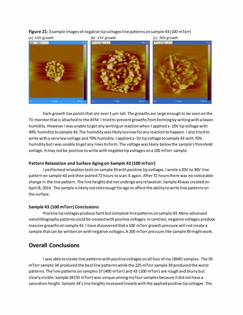
Figure 21: Example images of negative tip voltages line patterns on sample 43 (100 mTorr)
(a) -10V growth (b) -15V growth (c) -30V growth
Each growth has points that are over 1 µm tall. The growths are large enough to be seen on the
TV monitor that is attached to the AFM. I tried to prevent growths from forming by writing with a lower
humidity. However I was unable to get any writing or reaction when I applied a -10V tip voltage with
40% humidity to sample 43. The humidity was likely too low for any reaction to happen. I also tried to
write with a very low voltage and 70% humidity. I applied a -5V tip voltage to sample 43 with 70%
humidity but I was unable to get any lines to form. The voltage was likely below the sample’s threshold
voltage. It may not be positive to write with negative tip voltages on a 100 mTorr sample.
Pattern Relaxation and Surface Aging on Sample 43 (100 mTorr)
I performed relaxation tests on sample 43 with positive tip voltages. I wrote a 20V to 30V line
pattern on sample 43 and then waited 72 hours to scan it again. After 72 hours there was no noticeable
change in the line pattern. The line heights did not undergo any relaxation. Sample 43 was created on
April 8, 2014. The sample is likely not old enough for age to affect the ability to write line patterns on
the surface.
Sample 43 (100 mTorr) Conclusions
Positive tip voltages produce faint but complete line patterns on sample 43. More advanced
nanolithography patterns could be created with positive voltages. In contrast, negative voltages produce
massive growths on sample 43. I have discovered that a 100 mTorr growth pressure will not create a
sample that can be written on with negative voltages. A 200 mTorr pressure like sample 39 might work.
Overall Conclusions
I was able to create line patterns with positive voltages on all four of my LBMO samples. The 50
mTorr sample 34 produced the best line patterns while the 225 mTorr sample 39 produced the worst
patterns. The line patterns on samples 37 (400 mTorr) and 43 (100 mTorr) are rough and blurry but
clearly visible. Sample 34 (50 mTorr) was unique among my four samples because it did not have a
saturation height. Sample 34’s line heights increased linearly with the applied positive tip voltages. The

other three samples all had saturation heights at very high voltages. Sample 34’s lack of a saturation
height may be due to its low growth pressure and oxygen concentration.
I have successfully written on LBMO with negative tip voltages. I have discovered that the
growth pressure used during pulsed laser deposition can determine whether writing on a sample with
negative voltages is possible. There is a certain growth pressure above which negative line patterns can
be written on LBMO. This growth pressure is approximately 200 mTorr. Applying a negative voltage to a
sample that was created at less than 200 mTorr pressure will cause a massive growth to form. The
difference in results may be due to the sample’s oxygen concentration which is determined by the
sample’s growth pressure. High growth pressures create a large oxygen concentration in the sample.
Overall, more research is needed to determine exactly why the massive growths occur.
References
1) Li, R-W. (2009) ‘AFM lithography and fabrication of multifunctional nanostructures with perovskite
oxides’, Int. J. Nanotechnol., Vol. 6, No. 12, pp. 1067-1085.
Sample Data Table: LBMO-STO-37 (400 mTorr) Positive voltage data
LBMO-STO-37 Positive Tip Voltages400 mTorr Sample Line Heights (nm) in cells
Line Heights Dates, Test Number, and Line Type
September 25 September 27 September 27 November 8 September 9 September 30 September 30 September 30 September 30
Standard Test 5 Test 6 Test 7 Test 15 Test 2 Test 8 Test 9 Test 10 Test 11
Voltage (V) Average (nm) Deviation Decent Lines Decent Lines Faint Lines Decent Lines Faint Lines Faint Lines Blurry Lines Decent Lines Rough Lines
10 3.06 0.113137085 No Line 2.98 3.14
11 2.6767 0.30892286 2.62 2.40 3.01
12 2.4167 0.387341365 1.97 2.62 2.66
13 2.5333 0.270246801 2.84 2.43 2.33
14 2.6333 0.37072002 2.66 2.99 2.25
15 2.925 0.772765596 2.42 3.36 2.14 3.78
16 3.095 1.234868414 2.72 2.82 1.98 4.86
17 3.175 1.27039364 3.44 2.68 1.79 4.79
18 3.2725 1.168799241 3.10 2.90 2.17 4.92
19 2.8375 1.263576274 2.17 2.88 1.71 4.59
20 2.6314 0.851046974 2.51 2.81 2.16 4.41 2.29 1.75 2.49
21 2.505 1.539274721 4.81 1.86 1.65 1.70
22 2.24 0.697471624 2.46 3.05 1.39 2.06
23 2.29 1.284653001 4.10 2.31 1.37 1.38
24 2.46 1.386755806 4.52 1.72 1.56 2.05
25 2.59 0.836953802 3.77 1.92 2.08 2.58
26 2.5867 1.046438404 3.33 1.39 3.04
27 2.5767 1.127578526 3.50 1.32 2.91
28 3.12 0.340734501 3.51 2.88 2.97
29 2.9467 0.920452787 3.85 2.98 2.01
30 3.748 1.076229529 3.72 2.01 4.74 4.54 3.73
31 3.56 0.183847763 3.43 3.69
32 3.975 0.403050865 4.26 3.69
33 4.105 0.572756493 3.70 4.51
34 4.015 0.643467171 3.56 4.47
35 3.825 0.714177849 3.32 4.33
36 4.115 0.374766594 3.85 4.38
37 4.195 0.106066017 4.27 4.12
38 4.18 0.410121933 3.89 4.47
39 4.44 0.254558441 4.62 4.26
40 4.32 0.692964646 3.83 4.81