chemically derived cuo/in2o3 based nanocomposite for diode ... filechemically derived cuo/in2o3...
TRANSCRIPT

1
SUPPORTING INFORMATION
Chemically derived CuO/In2O3 based nanocomposite for diode applications
G. Mohan Kumara*, P. Ilanchezhiyana, A. Madhan Kumarb, T. S. Shabic,
S. Tamil Selvand, S. Sureshe, Sh. U. Yuldasheva and T. W. Kanga*
aQuantum-Functional Semiconductor Research Center,
Dongguk University, Seoul, Republic of Korea.
bCenter of Research Excellence in Corrosion,
King Fahd University of Petroleum & Minerals, Kingdom of Saudi Arabia.
cDepartment of Polymer Science and Engineering
Zhejiang University, Hangzhou, China.
dAdvanced Materials Processing and Analysis Center ,
NanoScience Technology Center, Materials Science Engineering,
University of Central Florida, Orlando, USA.
eGT-CNRS-UMI Lab, Georgia Institute of Technology,
2-3, rue Marconi, Metz, France.
Fax: +82-2-2278-4519; Tel: +82-10-4896-1777
Email: [email protected], [email protected]
Electronic Supplementary Material (ESI) for CrystEngComm.This journal is © The Royal Society of Chemistry 2015

2
Energy-dispersive X-ray spectroscopy (EDS): Thin films of Cu-In-O that were obtained
through a traditional drop casting route on glass substrates were used to record the EDS
spectrum. The purpose of such examination was to quantify the content of Cu and In
elements present in the composite systems. Here, the weight ratio between Cu, In and O
elements was found to be 60, 12 and 28 respectively. The analysis was carried out on 2-3
different areas, which hardly revealed any difference in the same.
Figure S1: EDS spectrum of Cu-In-O composites and the corresponding area scanned is
shown in the SEM image.

3
Preparation of Cu-In-O dispersions: 10 mg of the processed Cu-In-O powders were
initially dispersed in 15-25 ml of ethanol and subjected to sonication for a period of 30 min
and subsequently aged for 6-12 h. The ageing process was carried out to separate the larger
particulates (through decantation) from the colloidal media. The resulting sol was then used
to record the UV-vis absorbance spectrum and for TEM measurements. The same was also
used in the fabrication of Cu-In-O made working electrodes and establish p-type active layers
on ZnO nanowires via drop casting.
Hydrothermal growth of ZnO nanowires: ITO substrates pre-cleaned using acetone;
ethanol and deionized water were used to establish the ZnO seed layers via immersing the
same in a solution made of zinc acetate in ethanol (under stirring for a period of 15 min at
65-70 C). The substrates were then dried in a dry stream of nitrogen gas and annealed at
350 C for 30 min. 3-5 cycles were repeated to obtain uniform deposition of ZnO seed
layers. The prepared seed layers were then subjected to hydrothermal treatment in a
solution made of 25 mM zinc nitrate and hexamethylenetetramine, respectively. The
growth conditions for the nanowires involved their hydrothermal growth at 120 C/3-9 h.
The final products were washed with deionized water and annealed at 450 C for 30 min.
Figure S2: XRD pattern for ZnO nanowires on ITO.

4
Figure S3: Surface and cross-sectional SEM images revealing the excellent periodicity
among the hydrothermally grown ZnO nanowires.
Fabrication of Cu-In-O/ZnO heterostructures: The Cu-In-O made colloidal dispersion
was drop casted on the hydrothermally grown ZnO nanowires at room temperature. After the
solvents evaporate, the film was heat treated on a hot plate at 150 C for 10 min. Similarly, a
maximum of 10 cycles were repeated to attain the active layer with considerable thickness.
The resulting heterostructures were finally annealed at 400 C for 30 min, prior to the I-V
measurements. However, to elucidate the function of thickness of Cu-In-O deposits on the
diode behaviour, heterostructures were prepared via varying the drop cast cycles in an
ascending manner.
Figure S4: Cross-sectional representation of Cu-In-O/ZnO made p-n heterostructures
obtained through (a, b) 5 and (c, d) 5 drop cast cycles.

5
Charge transfer mechanism in Cu-In-O/ZnO made p-n heterostructures: The
schematic energy level diagram proposed in Figure S5 could initially be held responsible for
the observed rectification behaviour in the constructed diodes. The schematic layout was
actually proposed after considering the existence of CuO and In2O3 in form of a blend in the
processed Cu-In-O systems. In the proposed step-wise architecture, when the composite
material comes in contact with the ZnO nanowires, a p-n junction is naturally established at
their heterostructure interface. This favourable band alignment then favours the facile
transport of electrons from the conduction band (EC) of CuO to the EC of ZnO and the hole
transport to take place from the valence band (EV) of ZnO to the EV of CuO. Additionally, the
In2O3 in between CuO and ZnO could also act as an inherent energy barrier and aid with the
passivation of surface traps (oxygen vacancies) over the nanowires (caused by the
introduction of Cu-In-O). This arrangement might in turn favour the charge transfer kinetics
across the device and may be held responsible for the improved rectifying character under
illumination. The concept of built-in potential has been additionally discussed in the main
text to correlate the improved charge transfer kinetics and rectification behaviour under
illumination.
Figure S5: Schematic energy level diagram corresponding to the fabricated heterostructures.

6
Effect of thickness of Cu-In-O deposits on the I-V performance: The number of drop
cast cycles was actually varied during the fabrication of heterostructures to study the
influence of thickness of Cu-In-O deposits on the I-V characteristics of Cu-In-O/ZnO
made diodes. Figure S6 shows the I-V characteristics that were recorded for the diodes
that were fabricated under less than 5 drop cast cycles. Here, the obtained results suggest
the constructed devices to produce a higher current under negative bias, affirming the
reverse rectifying characteristics under dark and illuminated conditions. The observed
characteristics could be attributed to the oxygen related defects, as made clear from the
XPS and PL measurements. The extra electrons existing within the oxygen defects might
have acted as donor-like states, enabling the realization of an accumulation layer near the
interface [1]. This phenomenon in turn could have directed the bands in ZnO to bend
downwards, resulting with the e- accumulation to take place on ZnO side. And, this
reverse band bending could have strengthened further under forward bias, thereby
restricting the easy flow of carriers and resulting with the observed characteristics.
Figure S6: I-V characteristics of Cu-In-O/ZnO made p-n heterostructures that were obtained
via drop casting the colloidal Cu-In-O suspension on ZnO for 5 times.

7
I-V characteristics of Cu-In-O/ZnO heterostructures: When the drop cast cycles was
held 5, the current values were noted to increase significantly under forward bias and
decrease under reverse bias. This behaviour could be attributed to the weakening of
reverse band bending, which in turn favours the facile transport of charge carriers across
the device structures [2]. The concept of built-in potential is actually discussed in the
main script to assimilate the improved rectification properties upon photon illumination.
Figure S7: I-V characteristics of Cu-In-O/ZnO made p-n heterostructures that were obtained
via drop casting the colloidal Cu-In-O suspension on ZnO for 5 times.

8
Mott-Schottky (MS) plots: The MS plot for D1 and D2 i.e. for ZnO and Cu-In-O was studied
through a potential scan method under an applied frequency of 100 Hz. The experiments
were carried out through exposing 1 cm2 of the electrode material to a standard phosphate
based buffer solution (pH 6/7). Such analysis was used to personify the n-type and p-type
conductivity (from the positive and negative slopes) in ZnO and Cu-In-O, respectively [1-4].
The origin of their conductivity could be correlated with the existence of intrinsic defects
(such as the negatively charged copper/zinc vacancies or interstitial oxygen) associated
within the composite systems. The VFB for the geometrically exposed area was estimated to
be around -0.25 and -0.09 V (SCE) for D1 and D2, while their corresponding carrier density
was calculated to be around 1020 and 1018 cm-3, respectively.
Figure S8: Mott-Schottky (MS) plots signifying the n-type and p-type behaviour in ZnO and
Cu-In-O made working electrodes at an applied frequency of 100 Hz.
9
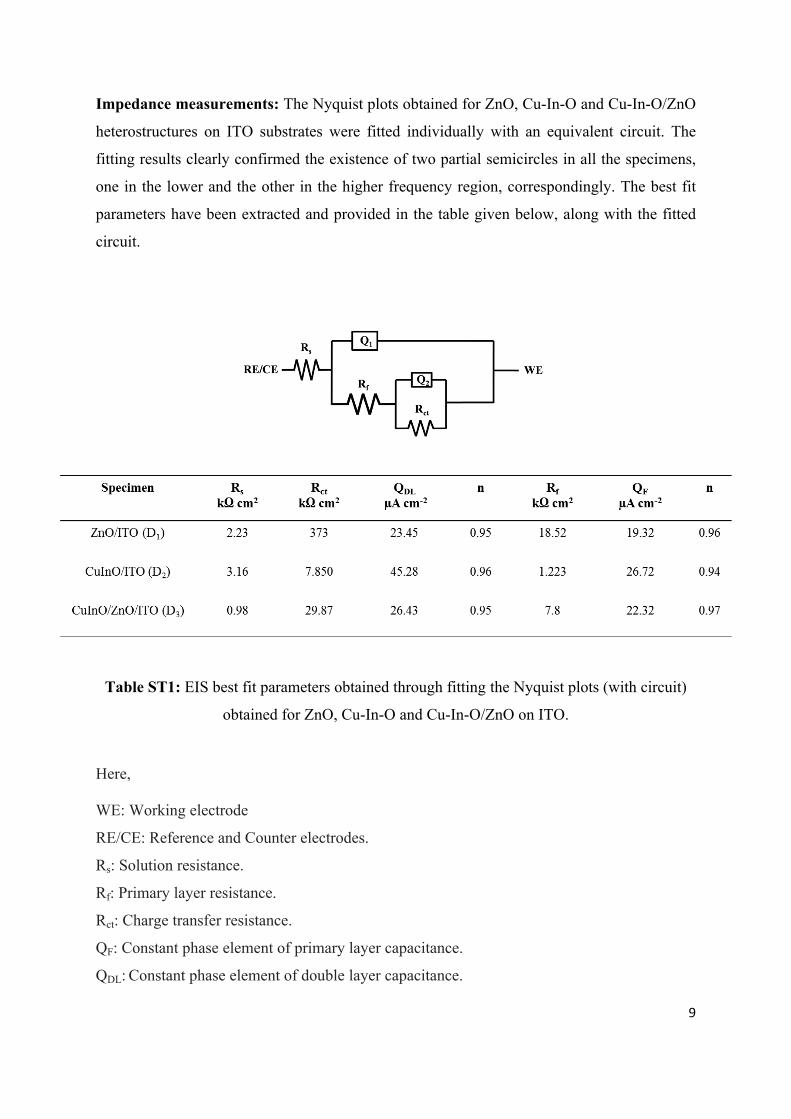
Impedance measurements: The Nyquist plots obtained for ZnO, Cu-In-O and Cu-In-O/ZnO
heterostructures on ITO substrates were fitted individually with an equivalent circuit. The
fitting results clearly confirmed the existence of two partial semicircles in all the specimens,
one in the lower and the other in the higher frequency region, correspondingly. The best fit
parameters have been extracted and provided in the table given below, along with the fitted
circuit.
Table ST1: EIS best fit parameters obtained through fitting the Nyquist plots (with circuit)
obtained for ZnO, Cu-In-O and Cu-In-O/ZnO on ITO.
Here,
WE: Working electrode
RE/CE: Reference and Counter electrodes.
Rs: Solution resistance.
Rf: Primary layer resistance.
Rct: Charge transfer resistance.
QF: Constant phase element of primary layer capacitance.
QDL: Constant phase element of double layer capacitance.

10
References:
1. U. Diebold, Surf. Sci. Rep., 2003, 48, 53.
2. K. Bimal Sarma, R. Arup Pal, Heremba Bailung and Joyanti Chutia, J. Phys. D: Appl.
Phys., 2012, 45, 275401.
3. F. Charles Windisch and J. Gregory Exarhos, J. Vac. Sci. Technol. A, 2000, 18, 1677.
4. A. Wolcott, W. A. Smith, T. R. Kuykendall, Y. Zhao and J. Z. Zhang, Adv. Funct.
Mater., 2009, 19, 1849.
5. O. Musa, T. Akomolafe and M. J. Carter, Sol. Energy Mater. Solar Cells, 1998, 51,
305.
6. Andreas Othonos and Matthew Zervos, Nanoscale Res. Lett., 2011, 6, 622.