charge storage mechanism of si nanocrystals … zhang1, sam zhang1, ming yang2, and tupei chen2...
TRANSCRIPT

Delivered by Ingenta toNanyang Technological University
IP 15569210Wed 14 Apr 2010 042212
Copyright copy 2009 American Scientific PublishersAll rights reservedPrinted in the United States of America
Nanoscience andNanotechnology LettersVol 1 176ndash181 2009
Charge Storage Mechanism of Si NanocrystalsEmbedded SiO2 Films
Wali Zhang1 Sam Zhang1lowast Ming Yang2 and Tupei Chen21School of Mechanical and Aerospace Engineering Nanyang Technological University
50 Nanyang Avenue 639798 Singapore2School of Electrical and Electronic Engineering Nanyang Technological University
50 Nanyang Avenue 639798 Singapore
SiO15SiO03SiO15 sandwich structure was synthesized by reactive magnetron sputtering to achievevarious densities of Si nanocrystals and different concentration of Si suboxides X-ray photoelectronspectroscopy is employed for depth profiling of the chemical structure and charging effect of thesandwich structure The Si 2p core-levels are found to strongly shift to higher binding energyThe shift can be ascribed to the photoemission-induced charging effect The opposite trend ofthe charging effect to the concentration of Si suboxides (Si2O SiO and Si2O3 indicates that thedefects are not responsible for the charge mechanism The Si nanocrystals concentration dependentcharging effect suggests that the nc-Si plays a dominant role for the charge trapping in such films
Keywords Si Nanocrystals Si Suboxides Charging Effect X-ray Photoelectron Spectroscopy
SiO2 films embedded with Si nanocrystals (nc-Si) haveattracted an increasing attention over the past decadesdue to potential applications in non-volatile flash mem-ory where fast writeerase speed long retention time andsuperior endurance with non-destructive read have beendemonstrated12 To date understanding of the charge trap-ping and retention mechanism in such nanostructures isstill unclear Several models for long-time charge trappingmechanisms have been proposed including the quantumsize effect of nc-Si and various oxygen-related defectsThe observation of quantum confinement energy in nc-Sifrom high-frequency conductance characteristics3 and theCoulomb blockade charging in the conductancendashvoltagemeasurements suggest that the charges are stored in thenc-Si4ndash6 Shi et al7 had compared the electrical behaviorsof the MOS diodes annealed in H2 ambient (low defectscondition due to the H2 passivation) with that of MOSdiodes annealed in vacuum (high defects condition) Theirinvestigation demonstrated that the defects play an impor-tant role for the charge storage It is still in debate whetherthe charges trap mainly in the defects or in the nc-SiIn this study X-ray photoelectron spectroscopy (XPS)
technique is employed to characterize the chemical struc-ture and binding energy shift of the nc-Sia-SiO2 sys-tem It has been reported that the X-ray radiation willleave positive charges in the nc-Sia-SiO2 system due to
lowastAuthor to whom correspondence should be addressed
photoemission89 The charging effect can cause the core-level to shift to a higher binding energy1011 In this paperSiO15SiO03SiO15 sandwich structure was synthesizedby reactive magnetron sputtering to deliberately achievevarious concentrations of nc-Si and Si suboxides (poten-tially contain high density of oxygen-related defects) XPSdepth profiling was carried out on the sandwich structureBy examining the changes of charging effect versus thedepth distributions of nc-Si and Si suboxides the nc-Siwas found responsible for the charge trapping mechanismrather than the defects in the oxidesThe SiO15SiO03SiO15 sandwich structure was synthe-
sized by a reactive magnetron sputtering system (E303APenta Vacuum) from a 4-inch Si target (99999 in purity)in a mixed ArO2 atmosphere on P-type (100) Si waferThe concentration of Si in each SiOx (0ltx lt 2) sub-layerwas controlled by the ratio of the ArO2 flow rate Thebase pressure of the deposition chamber was 10times10minus5 PaDuring deposition the radio frequency (136 MHz) targetpower was fixed at 150 W The process pressure and theAr flow rate were fixed at 05 Pa and 80 sccm respec-tively First the oxygen flow rate was set at 15 sccm todeposit the 10 nm relatively low Si concentration bottomlayer Immediately after that the shutter (between the sub-strate and the target) was closed and the oxygen flow ratewas changed to 05 sccm A waiting time of 10 minuteswas respected to achieve the desired stable ArO2 ambi-ent before sputtering the 10 nm high Si concentration
176 Nanosci Nanotechnol Lett 2009 Vol 1 No 3 1941-490020091176006 doi101166nnl20091032
Delivered by Ingenta toNanyang Technological University
IP 15569210Wed 14 Apr 2010 042212
Zhang et al Charge Storage Mechanism of Si Nanocrystals Embedded SiO2 Films
middle layer Finally the shutter was closed again andthe oxygen flow rate was changed back to 15 sccmThe 10 nm low Si concentration top layer was depositedafter another waiting time of 10 minutes A pure a-SiO2
control sample was also deposited by setting the oxygenflow rate at 30 sccm Thermal annealing was carried outin N2 ambient at 1100 C for 30 minutes XPS analy-sis was performed by using a Kratos-Axis spectrometerwith monochromatic Al K (148671 eV) X-ray radiationThe core-level spectra were recorded using pass energyof 40 eV at a normal emission angle The depth profilingwas realized by Ar ion sputtering which was carried outin situ with the XPS measurement The formation of nc-Siwas confirmed using transition electron microscopy (TEMJEM2010)Figure 1 shows the cross-sectional TEM micrograph of
the sandwich structure Nearly spherical-shaped nc-Si inthe amorphous matrix of SiO2 are clearly visible in theHRTEM micrograph There are densely stacked nc-Si inthe high Si middle layer and isolated nc-Si in the low Sitop and bottom layer The nc-Si size ranged from 3 to5 nm resulting in a mean crystal size of 4 nm in diameterIt has been well known that X-ray irradiation can cause
charging on the nc-Sia-SiO2 system The photoemissionduring the XPS measurement will leave positive chargesin the SiO2 films embedded with nc-Si leading to a core-level shift to a higher binding energy810ndash12 Figure 2 showthe contaminated C 1s core-level spectra from the surfaceof the sandwich structure which was embedded with nc-Siand the pure SiO2 control sample respectively The charg-ing effect induced by the photoemission can be clearlyobserved by the C 1s core-level shift The C 1s core-levelof the pure SiO2 control sample has a shift of sim06 eVrelative to the reference (2845 eV)11 while the C 1s peakof the sandwich structure that contains nc-Si shows a shift
Fig 1 TEM micrograph of the SiO15SiO03SiO15 sandwich structure
Fig 2 C 1s core-level shift relative to the reference for the pure SiO2
control sample and the sandwich structure
of sim18 eV The C 1s core-level shift coincides with thatof Si4+ 2p shown in Figure 3 The Si4+ 2p core-levels alsoshift to higher binding energy by 06 eV and 18 eV forthe pure SiO2 sample and the sandwich structure respec-tively Since Si4+ is the host material in the nc-SiSiO2
system under study therefore the Si4+ shift is used formonitoring the charging effect in the system during depthprofiling The introduction of the nc-Si into the SiO2 canshift the core-level to higher binding energy by 12 eVwhich indicates that the charging capability of the nc-Siembedded SiO2 films is greatly enhanced comparing withthat of the pure SiO2 However it is reported that for thenc-Si embedded SiO2 system the charges can be trappedeither inside the nc-Si or the defects in the oxides As atthe same time that the nc-Si is introduced into the SiO2a large amount of Si suboxides (Si2O SiO Si2O3 whichpotential contain high density of oxygen related-defectswere also produced These defects were reported to be the
Fig 3 Si 2p core-level spectra obtained from the surface of theSiO15SiO03SiO15 sandwich structure and the pure SiO2 control sample
Nanosci Nanotechnol Lett 1 176ndash181 2009 177
Delivered by Ingenta toNanyang Technological University
IP 15569210Wed 14 Apr 2010 042212
Charge Storage Mechanism of Si Nanocrystals Embedded SiO2 Films Zhang et al
weak oxygen bond (OndashO)13 the neutral oxygen vacancy(O3equivSindashSiequivO3 where equiv represents the bonds to threeoxygen atoms)13 Eprime
center (O3equivSi bull+ SiequivO3 where bullrepresents an unpaired electron and + is an trapped hole)14
and the non-bridging oxygen hole center (equivSindashObull)15 Bydepth profiling of the SiO15SiO03SiO15 sandwich struc-ture we are able to obtain the distribution of the nc-Si andSi suboxides By monitoring the changes of the chargingeffects versus the concentration of nc-Si and Si suboxidesone may be able figure out the charge trapping mecha-nisms of the nc-Si embedded SiO2 systemsNote should be taken that our Si-rich oxide films were
synthesized by reaction of the sputtered Si atoms with oxy-gen It was therefore quite possible that the oxidation pro-ceeded with zero one two three or all four SindashSi bondsbeing replaced by SindashO bonds We thus expect five oxi-dation states Sin+ (n = 0 1 2 3 and 4) corresponding tothe five chemical structures including Si Si2O SiO Si2O3
and SiO2 respectively exist in the magnetron sputteredfilms With the possible existence of the five oxidationstates in mind deconvolution of the XPS curves was carryout by decomposing the spectrum into five Gaussian peaksfollowing the reported fitting procedures16 The deconvo-lution of XPS curve was conducted by decomposing the Si2p line into Si 2p12 and Si 2p32 lines with intensity ratio12 and a fixed spin-orbit splitting of 06 eV as an atomicproperty Only the sum of the Si 2p12 and 2p32 partnerlines is shown for a clear presentation The full width athalf maximum (2 ) was assumed to be the same for bothlines but allowed to vary from Si0 to Si4+ and the relativeweight (W ) was allowed to vary without constraint The
(a) (b)
(c) (d)
Fig 4 Si 2p core-level spectra obtained at the depth of 2 nm (a) at the depth of 8 nm (b) at the depth of 12 nm (c) and at the depth of 22 nm (d)
deconvolution of the Si 2p spectra at different depths isshown in Figure 4 Figures 4(a)ndash(d) show the Si 2p core-levels at the depths of 2 nm 8 nm 12 nm and 22 nmrespectively The total Si concentration is calculated to besim40 at in both the low Si top and bottom layer andincrease to sim76 at in the high Si middle layer The Si2p spectrum shown in Figure 4(b) (at the depth of 8 nm)is speculated to be obtained at the interface between thetop layer and the middle layerAs can be observed from Figure 4 not only the total Si
concentration changes with the depth but the peak areasof the five oxidation states also change showing that theconcentrations of the five oxidation states vary with thedepth The depth distribution of the relative concentrationof each oxidation state can be obtained by calculating theratio of In+Si Itotal (n = 0 1 2 3 and 4) at various depthswhere In+Si is the peak area of the oxidation state Sin+
and Itotal is the total area of the Si 2p peaks The sumof the relative concentrations of Si suboxides (Si2O SiOand Si2O3 and nc-Si (Si0 versus the depth are shownin Figure 5 From the depth distribution of the Si sub-oxides and the nc-Si one can observe that different con-centrations of nc-Si and Si suboxides along depth havebeen achieved in our SiO15SiO03SiO15 sandwich struc-ture The majority Si atoms in the low Si top and bottomlayer have been oxidized into SiO2 leaving only smallamount of Si suboxides and low density of nc-Si whilethere are high concentration of Si suboxides and high den-sity of nc-Si in the high Si middle layer For example theconcentrations of the nc-Si are sim9 at in the low Si topand bottom layer sim51 at in the high Si middle layer
178 Nanosci Nanotechnol Lett 1 176ndash181 2009
Delivered by Ingenta toNanyang Technological University
IP 15569210Wed 14 Apr 2010 042212
Zhang et al Charge Storage Mechanism of Si Nanocrystals Embedded SiO2 Films
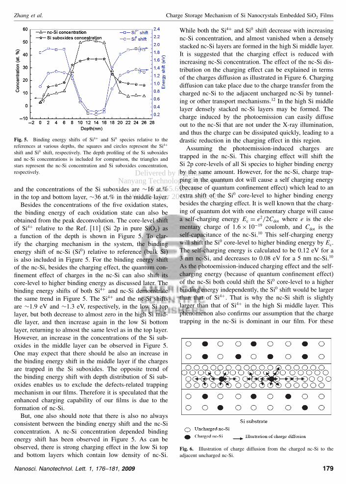
Fig 5 Binding energy shifts of Si4+ and Si0 species relative to thereferences at various depths the squares and circles represent the Si4+
shift and Si0 shift respectively The depth profiling of the Si suboxidesand nc-Si concentrations is included for comparison the triangles andstars represent the nc-Si concentration and Si suboxides concentrationrespectively
and the concentrations of the Si suboxides are sim16 atin the top and bottom layer sim36 at in the middle layerBesides the concentrations of the five oxidation states
the binding energy of each oxidation state can also beobtained from the peak deconvolution The core-level shiftof Si4+ relative to the Ref [11] (Si 2p in pure SiO2 asa function of the depth is shown in Figure 5 To clar-ify the charging mechanism in the system the bindingenergy shift of nc-Si (Si0 relative to reference (bulk Si)is also included in Figure 5 For the binding energy shiftof the nc-Si besides the charging effect the quantum con-finement effect of charges in the nc-Si can also shift itscore-level to higher binding energy as discussed later Thebinding energy shifts of both Si4+ and nc-Si demonstratethe same trend in Figure 5 The Si4+ and the nc-Si shiftsare sim19 eV and sim13 eV respectively in the low Si toplayer but both decrease to almost zero in the high Si mid-dle layer and then increase again in the low Si bottomlayer returning to almost the same level as in the top layerHowever an increase in the concentrations of the Si sub-oxides in the middle layer can be observed in Figure 5One may expect that there should be also an increase inthe binding energy shift in the middle layer if the chargesare trapped in the Si suboxides The opposite trend ofthe binding energy shift with depth distribution of Si sub-oxides enables us to exclude the defects-related trappingmechanism in our films Therefore it is speculated that theenhanced charging capability of our films is due to theformation of nc-SiBut one also should note that there is also no always
consistent between the binding energy shift and the nc-Siconcentration A nc-Si concentration depended bindingenergy shift has been observed in Figure 5 As can beobserved there is strong charging effect in the low Si topand bottom layers which contain low density of nc-Si
While both the Si4+ and Si0 shift decrease with increasingnc-Si concentration and almost vanished when a denselystacked nc-Si layers are formed in the high Si middle layerIt is suggested that the charging effect is reduced withincreasing nc-Si concentration The effect of the nc-Si dis-tribution on the charging effect can be explained in termsof the charges diffusion as illustrated in Figure 6 Chargingdiffusion can take place due to the charge transfer from thecharged nc-Si to the adjacent uncharged nc-Si by tunnel-ing or other transport mechanisms12 In the high Si middlelayer densely stacked nc-Si layers may be formed Thecharge induced by the photoemission can easily diffuseout to the nc-Si that are not under the X-ray illuminationand thus the charge can be dissipated quickly leading to adrastic reduction in the charging effect in this regionAssuming the photoemission-induced charges are
trapped in the nc-Si This charging effect will shift theSi 2p core-levels of all Si species to higher binding energyby the same amount However for the nc-Si charge trap-ping in the quantum dot will cause a self charging energy(because of quantum confinement effect) which lead to anextra shift of the Si0 core-level to higher binding energybesides the charging effect It is well known that the charg-ing of quantum dot with one elementary charge will causea self-charging energy Ec = e22Cdot where e is the ele-mentary charge of 16times 10minus19 coulomb and Cdot is theself-capacitance of the nc-Si10 This self-charging energywill shift the Si0 core-level to higher binding energy by EcThe self-charging energy is calculated to be 012 eV for a3 nm nc-Si and decreases to 008 eV for a 5 nm nc-Si10
As the photoemission-induced charging effect and the self-charging energy (because of quantum confinement effect)of the nc-Si both could shift the Si0 core-level to a higherbinding energy independently the Si0 shift would be largerthan that of Si4+ That is why the nc-Si shift is slightlylarger than that of Si4+ in the high Si middle layer Thisphenomenon also confirms our assumption that the chargetrapping in the nc-Si is dominant in our film For these
Fig 6 Illustration of charge diffusion from the charged nc-Si to theadjacent uncharged nc-Si
Nanosci Nanotechnol Lett 1 176ndash181 2009 179
Delivered by Ingenta toNanyang Technological University
IP 15569210Wed 14 Apr 2010 042212
Charge Storage Mechanism of Si Nanocrystals Embedded SiO2 Films Zhang et al
nc-Si distributed in the low Si top and bottom layer theyare separated from each other with a larger spacing due tothe low concentration thus the charge diffusion is muchmore difficult to take place Therefore the charging effectis much more significant in these two regionsAs discussed above for Si0 besides the charging effect
the quantum size effect of nc-Si will increase the Si0
shift one may also expected a higher binding energy shiftof Si0 than that of Si4+ in the low Si top and bottomlayer However quite contrarily a smaller binding energyshift of Si0 than that of Si4+ is always observed in thesetwo regions as shown in Figure 5 This can be inter-preted by the differential charging (electrostatic charging)effect between the nc-Si and the oxide matrix811 Differ-ential charging always occur when the sample is partially(semi)conducting and partially insulating under X-ray radi-ation This differential charging usually lead to the varia-tion in Si4+ndashSi0 shift with different Si concentration8911
Note that the kinetic energy of the photoelectrons underX-ray radiation can be simply written as
EK = hvminusEB minusS minusq (1)
where hv is the X-ray energy EB is the binding energyS is the work function of the electron spectrometer q isthe electronic charge and is the surface potential Sincethe experiments were performed using the same spectrom-eter thus the effect of the spectrometer work function (Son the Si4+ndashSi0 shift should be negligible Therefore itcan only be differences in the material surface potentialthat can contribute to Si4+ndashSi0 shift When characterizingnc-SiSiO2 system one usually assumes that the surfacepotential is the same for Si0 and Si4+ However the dif-ferential charging lead to the surface potential differencesbetween Si0 and Si4+ thus the Si4+ndashSi0 shift in the nc-SiSiO2 system not only determined by the their chemi-cal shift but also their surface potential differences Thepositive charges lead to the reduction in Si0 surface poten-tial while the increase in Si4+ surface potential equiva-lent to a reduction in S0 binding energy and an increasein Si4+ binding energy The Si4+ndashSi0 shift may vary from35ndash50 eV depending on the nc-Si concentration in thefilms8911 The Si4+ndashSi0 shift decrease with increase nc-Siconcentration and will be the same as that of bulk refer-ence samples when densely stacked nc-Si are formed Thechanges of Si4+ndashSi0 shift with nc-Si concentration can beemployed to interpret why there is no always consistencybetween the binding energy shift of Si0 and Si4+ along thedepth Figure 7 shows the Si4+ndashSi0 chemical shift versusdepth of the sandwich structure and the depth distributionof nc-Si also included for comparison The Si4+ndashSi0 shiftis sim44 eV in the low Si top and bottom layer which con-tain low density of nc-Si However densely stacked nc-Siare formed in the high Si middle layer and the Si4+ndashSi0
shift is almost the same as the bulk references The charg-ing effect cause almost the same core-level shift of both
Fig 7 Si4+ndashSi0 shift versus depth The depth distribution of nc-Si isincluded for comparison
Si0 and Si4+ while the quantum size effect of nc-Si leadto the core-level shift slightly larger than that of Si4+
In conclusion various concentrations of Si suboxidesand Si nanocrystals (nc-Si) have been realized by sputter-ing deposition of SiO15SiO03SiO15 sandwich structureThe X-ray radiation shifts the Si 2p core-levels to higherbinding energy due to the photoemission-induced chargingeffect The opposite trend of the binding energy shift tothe depth distribution of Si suboxides concentrations sug-gests that the oxygen-related defects are not responsiblefor charge trapping in the nc-SiSiO2 system The nc-Siconcentration dependent charging effect and the quantumcharging effect were observed which demonstrates that thenc-Si plays a dominant role in the charge trapping mecha-nism in the nc-Sia-SiO2 system The decreasing in bindingenergy shift with the increasing nc-Si concentration is dueto the charging diffusion
References and Notes
1 S Tiwari F Rana H Hanafi A Hartstein E F Crabbe andK Chan Appl Phys Lett 68 1377 (1996)
2 D Tsoukalas P Dimitrakis S Kolliopoulou and P Normand MatSci Eng B-Solid 124 93 (2005)
3 S Y Huang S Banerjee R T Tung and S Oda J Appl Phys94 7261 (2003)
4 L C Wu M Dai X F Huang Y J Zhang W Li J Xu and K JChen J Non-Cryst Solids 338ndash340 318 (2004)
5 C Dumas J Grisolia G BenAssayag C Bonafos S SchammA Claverie A Arbouet M Carrada V Paillard and M ShalchianPhysica E 38 80 (2007)
6 T Maeda E Suzuki I Sakata M Yamanaka and K Ishii Nano-technology 10 127 (1999)
7 Y Shi K Saito H Ishikuro and T Hiramoto J Appl Phys84 2358 (1998)
8 A Thogersen S Diplas J Mayandi T Finstad A Olsen J FWatts M Mitome and Y Bando J Appl Phys 103 024308 (2008)
9 F Karadas G Ertas and S Suzer J Phys Chem B 108 1515(2004)
10 T P Chen Y Liu C Q Sun M S Tse J H Hsieh Y QFu Y C Liu and S Fung J Phys Chem B 108 16609(2004)
180 Nanosci Nanotechnol Lett 1 176ndash181 2009
Delivered by Ingenta toNanyang Technological University
IP 15569210Wed 14 Apr 2010 042212
Zhang et al Charge Storage Mechanism of Si Nanocrystals Embedded SiO2 Films
11 A Dane U K Demirok A Aydinli and S Suzer J Phys Chem B110 1137 (2006)
12 T P Chen Y Liu M S Tse P F Ho G Dong and S Fung ApplPhys Lett 81 4724 (2002)
13 C J Lin C K Lee E W G Diau and G R Lin J ElectrochemSoc 153 E25 (2006)
14 G Buscarino S Agnello and F M Gelardi Mod Phys Lett B20 451 (2006)
15 S M Prokes and W E Carlos J Appl Phys 78 2671 (1995)16 F Rochet G Dufour H Roulet B Pelloie J Perriere
E Fogarassy A Slaoui and M Froment Phys Rev B 37 6468(1988)
Received 26 August 2009 Accepted 23 September 2009
Nanosci Nanotechnol Lett 1 176ndash181 2009 181

Delivered by Ingenta toNanyang Technological University
IP 15569210Wed 14 Apr 2010 042212
Zhang et al Charge Storage Mechanism of Si Nanocrystals Embedded SiO2 Films
middle layer Finally the shutter was closed again andthe oxygen flow rate was changed back to 15 sccmThe 10 nm low Si concentration top layer was depositedafter another waiting time of 10 minutes A pure a-SiO2
control sample was also deposited by setting the oxygenflow rate at 30 sccm Thermal annealing was carried outin N2 ambient at 1100 C for 30 minutes XPS analy-sis was performed by using a Kratos-Axis spectrometerwith monochromatic Al K (148671 eV) X-ray radiationThe core-level spectra were recorded using pass energyof 40 eV at a normal emission angle The depth profilingwas realized by Ar ion sputtering which was carried outin situ with the XPS measurement The formation of nc-Siwas confirmed using transition electron microscopy (TEMJEM2010)Figure 1 shows the cross-sectional TEM micrograph of
the sandwich structure Nearly spherical-shaped nc-Si inthe amorphous matrix of SiO2 are clearly visible in theHRTEM micrograph There are densely stacked nc-Si inthe high Si middle layer and isolated nc-Si in the low Sitop and bottom layer The nc-Si size ranged from 3 to5 nm resulting in a mean crystal size of 4 nm in diameterIt has been well known that X-ray irradiation can cause
charging on the nc-Sia-SiO2 system The photoemissionduring the XPS measurement will leave positive chargesin the SiO2 films embedded with nc-Si leading to a core-level shift to a higher binding energy810ndash12 Figure 2 showthe contaminated C 1s core-level spectra from the surfaceof the sandwich structure which was embedded with nc-Siand the pure SiO2 control sample respectively The charg-ing effect induced by the photoemission can be clearlyobserved by the C 1s core-level shift The C 1s core-levelof the pure SiO2 control sample has a shift of sim06 eVrelative to the reference (2845 eV)11 while the C 1s peakof the sandwich structure that contains nc-Si shows a shift
Fig 1 TEM micrograph of the SiO15SiO03SiO15 sandwich structure
Fig 2 C 1s core-level shift relative to the reference for the pure SiO2
control sample and the sandwich structure
of sim18 eV The C 1s core-level shift coincides with thatof Si4+ 2p shown in Figure 3 The Si4+ 2p core-levels alsoshift to higher binding energy by 06 eV and 18 eV forthe pure SiO2 sample and the sandwich structure respec-tively Since Si4+ is the host material in the nc-SiSiO2
system under study therefore the Si4+ shift is used formonitoring the charging effect in the system during depthprofiling The introduction of the nc-Si into the SiO2 canshift the core-level to higher binding energy by 12 eVwhich indicates that the charging capability of the nc-Siembedded SiO2 films is greatly enhanced comparing withthat of the pure SiO2 However it is reported that for thenc-Si embedded SiO2 system the charges can be trappedeither inside the nc-Si or the defects in the oxides As atthe same time that the nc-Si is introduced into the SiO2a large amount of Si suboxides (Si2O SiO Si2O3 whichpotential contain high density of oxygen related-defectswere also produced These defects were reported to be the
Fig 3 Si 2p core-level spectra obtained from the surface of theSiO15SiO03SiO15 sandwich structure and the pure SiO2 control sample
Nanosci Nanotechnol Lett 1 176ndash181 2009 177
Delivered by Ingenta toNanyang Technological University
IP 15569210Wed 14 Apr 2010 042212
Charge Storage Mechanism of Si Nanocrystals Embedded SiO2 Films Zhang et al
weak oxygen bond (OndashO)13 the neutral oxygen vacancy(O3equivSindashSiequivO3 where equiv represents the bonds to threeoxygen atoms)13 Eprime
center (O3equivSi bull+ SiequivO3 where bullrepresents an unpaired electron and + is an trapped hole)14
and the non-bridging oxygen hole center (equivSindashObull)15 Bydepth profiling of the SiO15SiO03SiO15 sandwich struc-ture we are able to obtain the distribution of the nc-Si andSi suboxides By monitoring the changes of the chargingeffects versus the concentration of nc-Si and Si suboxidesone may be able figure out the charge trapping mecha-nisms of the nc-Si embedded SiO2 systemsNote should be taken that our Si-rich oxide films were
synthesized by reaction of the sputtered Si atoms with oxy-gen It was therefore quite possible that the oxidation pro-ceeded with zero one two three or all four SindashSi bondsbeing replaced by SindashO bonds We thus expect five oxi-dation states Sin+ (n = 0 1 2 3 and 4) corresponding tothe five chemical structures including Si Si2O SiO Si2O3
and SiO2 respectively exist in the magnetron sputteredfilms With the possible existence of the five oxidationstates in mind deconvolution of the XPS curves was carryout by decomposing the spectrum into five Gaussian peaksfollowing the reported fitting procedures16 The deconvo-lution of XPS curve was conducted by decomposing the Si2p line into Si 2p12 and Si 2p32 lines with intensity ratio12 and a fixed spin-orbit splitting of 06 eV as an atomicproperty Only the sum of the Si 2p12 and 2p32 partnerlines is shown for a clear presentation The full width athalf maximum (2 ) was assumed to be the same for bothlines but allowed to vary from Si0 to Si4+ and the relativeweight (W ) was allowed to vary without constraint The
(a) (b)
(c) (d)
Fig 4 Si 2p core-level spectra obtained at the depth of 2 nm (a) at the depth of 8 nm (b) at the depth of 12 nm (c) and at the depth of 22 nm (d)
deconvolution of the Si 2p spectra at different depths isshown in Figure 4 Figures 4(a)ndash(d) show the Si 2p core-levels at the depths of 2 nm 8 nm 12 nm and 22 nmrespectively The total Si concentration is calculated to besim40 at in both the low Si top and bottom layer andincrease to sim76 at in the high Si middle layer The Si2p spectrum shown in Figure 4(b) (at the depth of 8 nm)is speculated to be obtained at the interface between thetop layer and the middle layerAs can be observed from Figure 4 not only the total Si
concentration changes with the depth but the peak areasof the five oxidation states also change showing that theconcentrations of the five oxidation states vary with thedepth The depth distribution of the relative concentrationof each oxidation state can be obtained by calculating theratio of In+Si Itotal (n = 0 1 2 3 and 4) at various depthswhere In+Si is the peak area of the oxidation state Sin+
and Itotal is the total area of the Si 2p peaks The sumof the relative concentrations of Si suboxides (Si2O SiOand Si2O3 and nc-Si (Si0 versus the depth are shownin Figure 5 From the depth distribution of the Si sub-oxides and the nc-Si one can observe that different con-centrations of nc-Si and Si suboxides along depth havebeen achieved in our SiO15SiO03SiO15 sandwich struc-ture The majority Si atoms in the low Si top and bottomlayer have been oxidized into SiO2 leaving only smallamount of Si suboxides and low density of nc-Si whilethere are high concentration of Si suboxides and high den-sity of nc-Si in the high Si middle layer For example theconcentrations of the nc-Si are sim9 at in the low Si topand bottom layer sim51 at in the high Si middle layer
178 Nanosci Nanotechnol Lett 1 176ndash181 2009
Delivered by Ingenta toNanyang Technological University
IP 15569210Wed 14 Apr 2010 042212
Zhang et al Charge Storage Mechanism of Si Nanocrystals Embedded SiO2 Films
Fig 5 Binding energy shifts of Si4+ and Si0 species relative to thereferences at various depths the squares and circles represent the Si4+
shift and Si0 shift respectively The depth profiling of the Si suboxidesand nc-Si concentrations is included for comparison the triangles andstars represent the nc-Si concentration and Si suboxides concentrationrespectively
and the concentrations of the Si suboxides are sim16 atin the top and bottom layer sim36 at in the middle layerBesides the concentrations of the five oxidation states
the binding energy of each oxidation state can also beobtained from the peak deconvolution The core-level shiftof Si4+ relative to the Ref [11] (Si 2p in pure SiO2 asa function of the depth is shown in Figure 5 To clar-ify the charging mechanism in the system the bindingenergy shift of nc-Si (Si0 relative to reference (bulk Si)is also included in Figure 5 For the binding energy shiftof the nc-Si besides the charging effect the quantum con-finement effect of charges in the nc-Si can also shift itscore-level to higher binding energy as discussed later Thebinding energy shifts of both Si4+ and nc-Si demonstratethe same trend in Figure 5 The Si4+ and the nc-Si shiftsare sim19 eV and sim13 eV respectively in the low Si toplayer but both decrease to almost zero in the high Si mid-dle layer and then increase again in the low Si bottomlayer returning to almost the same level as in the top layerHowever an increase in the concentrations of the Si sub-oxides in the middle layer can be observed in Figure 5One may expect that there should be also an increase inthe binding energy shift in the middle layer if the chargesare trapped in the Si suboxides The opposite trend ofthe binding energy shift with depth distribution of Si sub-oxides enables us to exclude the defects-related trappingmechanism in our films Therefore it is speculated that theenhanced charging capability of our films is due to theformation of nc-SiBut one also should note that there is also no always
consistent between the binding energy shift and the nc-Siconcentration A nc-Si concentration depended bindingenergy shift has been observed in Figure 5 As can beobserved there is strong charging effect in the low Si topand bottom layers which contain low density of nc-Si
While both the Si4+ and Si0 shift decrease with increasingnc-Si concentration and almost vanished when a denselystacked nc-Si layers are formed in the high Si middle layerIt is suggested that the charging effect is reduced withincreasing nc-Si concentration The effect of the nc-Si dis-tribution on the charging effect can be explained in termsof the charges diffusion as illustrated in Figure 6 Chargingdiffusion can take place due to the charge transfer from thecharged nc-Si to the adjacent uncharged nc-Si by tunnel-ing or other transport mechanisms12 In the high Si middlelayer densely stacked nc-Si layers may be formed Thecharge induced by the photoemission can easily diffuseout to the nc-Si that are not under the X-ray illuminationand thus the charge can be dissipated quickly leading to adrastic reduction in the charging effect in this regionAssuming the photoemission-induced charges are
trapped in the nc-Si This charging effect will shift theSi 2p core-levels of all Si species to higher binding energyby the same amount However for the nc-Si charge trap-ping in the quantum dot will cause a self charging energy(because of quantum confinement effect) which lead to anextra shift of the Si0 core-level to higher binding energybesides the charging effect It is well known that the charg-ing of quantum dot with one elementary charge will causea self-charging energy Ec = e22Cdot where e is the ele-mentary charge of 16times 10minus19 coulomb and Cdot is theself-capacitance of the nc-Si10 This self-charging energywill shift the Si0 core-level to higher binding energy by EcThe self-charging energy is calculated to be 012 eV for a3 nm nc-Si and decreases to 008 eV for a 5 nm nc-Si10
As the photoemission-induced charging effect and the self-charging energy (because of quantum confinement effect)of the nc-Si both could shift the Si0 core-level to a higherbinding energy independently the Si0 shift would be largerthan that of Si4+ That is why the nc-Si shift is slightlylarger than that of Si4+ in the high Si middle layer Thisphenomenon also confirms our assumption that the chargetrapping in the nc-Si is dominant in our film For these
Fig 6 Illustration of charge diffusion from the charged nc-Si to theadjacent uncharged nc-Si
Nanosci Nanotechnol Lett 1 176ndash181 2009 179
Delivered by Ingenta toNanyang Technological University
IP 15569210Wed 14 Apr 2010 042212
Charge Storage Mechanism of Si Nanocrystals Embedded SiO2 Films Zhang et al
nc-Si distributed in the low Si top and bottom layer theyare separated from each other with a larger spacing due tothe low concentration thus the charge diffusion is muchmore difficult to take place Therefore the charging effectis much more significant in these two regionsAs discussed above for Si0 besides the charging effect
the quantum size effect of nc-Si will increase the Si0
shift one may also expected a higher binding energy shiftof Si0 than that of Si4+ in the low Si top and bottomlayer However quite contrarily a smaller binding energyshift of Si0 than that of Si4+ is always observed in thesetwo regions as shown in Figure 5 This can be inter-preted by the differential charging (electrostatic charging)effect between the nc-Si and the oxide matrix811 Differ-ential charging always occur when the sample is partially(semi)conducting and partially insulating under X-ray radi-ation This differential charging usually lead to the varia-tion in Si4+ndashSi0 shift with different Si concentration8911
Note that the kinetic energy of the photoelectrons underX-ray radiation can be simply written as
EK = hvminusEB minusS minusq (1)
where hv is the X-ray energy EB is the binding energyS is the work function of the electron spectrometer q isthe electronic charge and is the surface potential Sincethe experiments were performed using the same spectrom-eter thus the effect of the spectrometer work function (Son the Si4+ndashSi0 shift should be negligible Therefore itcan only be differences in the material surface potentialthat can contribute to Si4+ndashSi0 shift When characterizingnc-SiSiO2 system one usually assumes that the surfacepotential is the same for Si0 and Si4+ However the dif-ferential charging lead to the surface potential differencesbetween Si0 and Si4+ thus the Si4+ndashSi0 shift in the nc-SiSiO2 system not only determined by the their chemi-cal shift but also their surface potential differences Thepositive charges lead to the reduction in Si0 surface poten-tial while the increase in Si4+ surface potential equiva-lent to a reduction in S0 binding energy and an increasein Si4+ binding energy The Si4+ndashSi0 shift may vary from35ndash50 eV depending on the nc-Si concentration in thefilms8911 The Si4+ndashSi0 shift decrease with increase nc-Siconcentration and will be the same as that of bulk refer-ence samples when densely stacked nc-Si are formed Thechanges of Si4+ndashSi0 shift with nc-Si concentration can beemployed to interpret why there is no always consistencybetween the binding energy shift of Si0 and Si4+ along thedepth Figure 7 shows the Si4+ndashSi0 chemical shift versusdepth of the sandwich structure and the depth distributionof nc-Si also included for comparison The Si4+ndashSi0 shiftis sim44 eV in the low Si top and bottom layer which con-tain low density of nc-Si However densely stacked nc-Siare formed in the high Si middle layer and the Si4+ndashSi0
shift is almost the same as the bulk references The charg-ing effect cause almost the same core-level shift of both
Fig 7 Si4+ndashSi0 shift versus depth The depth distribution of nc-Si isincluded for comparison
Si0 and Si4+ while the quantum size effect of nc-Si leadto the core-level shift slightly larger than that of Si4+
In conclusion various concentrations of Si suboxidesand Si nanocrystals (nc-Si) have been realized by sputter-ing deposition of SiO15SiO03SiO15 sandwich structureThe X-ray radiation shifts the Si 2p core-levels to higherbinding energy due to the photoemission-induced chargingeffect The opposite trend of the binding energy shift tothe depth distribution of Si suboxides concentrations sug-gests that the oxygen-related defects are not responsiblefor charge trapping in the nc-SiSiO2 system The nc-Siconcentration dependent charging effect and the quantumcharging effect were observed which demonstrates that thenc-Si plays a dominant role in the charge trapping mecha-nism in the nc-Sia-SiO2 system The decreasing in bindingenergy shift with the increasing nc-Si concentration is dueto the charging diffusion
References and Notes
1 S Tiwari F Rana H Hanafi A Hartstein E F Crabbe andK Chan Appl Phys Lett 68 1377 (1996)
2 D Tsoukalas P Dimitrakis S Kolliopoulou and P Normand MatSci Eng B-Solid 124 93 (2005)
3 S Y Huang S Banerjee R T Tung and S Oda J Appl Phys94 7261 (2003)
4 L C Wu M Dai X F Huang Y J Zhang W Li J Xu and K JChen J Non-Cryst Solids 338ndash340 318 (2004)
5 C Dumas J Grisolia G BenAssayag C Bonafos S SchammA Claverie A Arbouet M Carrada V Paillard and M ShalchianPhysica E 38 80 (2007)
6 T Maeda E Suzuki I Sakata M Yamanaka and K Ishii Nano-technology 10 127 (1999)
7 Y Shi K Saito H Ishikuro and T Hiramoto J Appl Phys84 2358 (1998)
8 A Thogersen S Diplas J Mayandi T Finstad A Olsen J FWatts M Mitome and Y Bando J Appl Phys 103 024308 (2008)
9 F Karadas G Ertas and S Suzer J Phys Chem B 108 1515(2004)
10 T P Chen Y Liu C Q Sun M S Tse J H Hsieh Y QFu Y C Liu and S Fung J Phys Chem B 108 16609(2004)
180 Nanosci Nanotechnol Lett 1 176ndash181 2009
Delivered by Ingenta toNanyang Technological University
IP 15569210Wed 14 Apr 2010 042212
Zhang et al Charge Storage Mechanism of Si Nanocrystals Embedded SiO2 Films
11 A Dane U K Demirok A Aydinli and S Suzer J Phys Chem B110 1137 (2006)
12 T P Chen Y Liu M S Tse P F Ho G Dong and S Fung ApplPhys Lett 81 4724 (2002)
13 C J Lin C K Lee E W G Diau and G R Lin J ElectrochemSoc 153 E25 (2006)
14 G Buscarino S Agnello and F M Gelardi Mod Phys Lett B20 451 (2006)
15 S M Prokes and W E Carlos J Appl Phys 78 2671 (1995)16 F Rochet G Dufour H Roulet B Pelloie J Perriere
E Fogarassy A Slaoui and M Froment Phys Rev B 37 6468(1988)
Received 26 August 2009 Accepted 23 September 2009
Nanosci Nanotechnol Lett 1 176ndash181 2009 181

Delivered by Ingenta toNanyang Technological University
IP 15569210Wed 14 Apr 2010 042212
Charge Storage Mechanism of Si Nanocrystals Embedded SiO2 Films Zhang et al
weak oxygen bond (OndashO)13 the neutral oxygen vacancy(O3equivSindashSiequivO3 where equiv represents the bonds to threeoxygen atoms)13 Eprime
center (O3equivSi bull+ SiequivO3 where bullrepresents an unpaired electron and + is an trapped hole)14
and the non-bridging oxygen hole center (equivSindashObull)15 Bydepth profiling of the SiO15SiO03SiO15 sandwich struc-ture we are able to obtain the distribution of the nc-Si andSi suboxides By monitoring the changes of the chargingeffects versus the concentration of nc-Si and Si suboxidesone may be able figure out the charge trapping mecha-nisms of the nc-Si embedded SiO2 systemsNote should be taken that our Si-rich oxide films were
synthesized by reaction of the sputtered Si atoms with oxy-gen It was therefore quite possible that the oxidation pro-ceeded with zero one two three or all four SindashSi bondsbeing replaced by SindashO bonds We thus expect five oxi-dation states Sin+ (n = 0 1 2 3 and 4) corresponding tothe five chemical structures including Si Si2O SiO Si2O3
and SiO2 respectively exist in the magnetron sputteredfilms With the possible existence of the five oxidationstates in mind deconvolution of the XPS curves was carryout by decomposing the spectrum into five Gaussian peaksfollowing the reported fitting procedures16 The deconvo-lution of XPS curve was conducted by decomposing the Si2p line into Si 2p12 and Si 2p32 lines with intensity ratio12 and a fixed spin-orbit splitting of 06 eV as an atomicproperty Only the sum of the Si 2p12 and 2p32 partnerlines is shown for a clear presentation The full width athalf maximum (2 ) was assumed to be the same for bothlines but allowed to vary from Si0 to Si4+ and the relativeweight (W ) was allowed to vary without constraint The
(a) (b)
(c) (d)
Fig 4 Si 2p core-level spectra obtained at the depth of 2 nm (a) at the depth of 8 nm (b) at the depth of 12 nm (c) and at the depth of 22 nm (d)
deconvolution of the Si 2p spectra at different depths isshown in Figure 4 Figures 4(a)ndash(d) show the Si 2p core-levels at the depths of 2 nm 8 nm 12 nm and 22 nmrespectively The total Si concentration is calculated to besim40 at in both the low Si top and bottom layer andincrease to sim76 at in the high Si middle layer The Si2p spectrum shown in Figure 4(b) (at the depth of 8 nm)is speculated to be obtained at the interface between thetop layer and the middle layerAs can be observed from Figure 4 not only the total Si
concentration changes with the depth but the peak areasof the five oxidation states also change showing that theconcentrations of the five oxidation states vary with thedepth The depth distribution of the relative concentrationof each oxidation state can be obtained by calculating theratio of In+Si Itotal (n = 0 1 2 3 and 4) at various depthswhere In+Si is the peak area of the oxidation state Sin+
and Itotal is the total area of the Si 2p peaks The sumof the relative concentrations of Si suboxides (Si2O SiOand Si2O3 and nc-Si (Si0 versus the depth are shownin Figure 5 From the depth distribution of the Si sub-oxides and the nc-Si one can observe that different con-centrations of nc-Si and Si suboxides along depth havebeen achieved in our SiO15SiO03SiO15 sandwich struc-ture The majority Si atoms in the low Si top and bottomlayer have been oxidized into SiO2 leaving only smallamount of Si suboxides and low density of nc-Si whilethere are high concentration of Si suboxides and high den-sity of nc-Si in the high Si middle layer For example theconcentrations of the nc-Si are sim9 at in the low Si topand bottom layer sim51 at in the high Si middle layer
178 Nanosci Nanotechnol Lett 1 176ndash181 2009
Delivered by Ingenta toNanyang Technological University
IP 15569210Wed 14 Apr 2010 042212
Zhang et al Charge Storage Mechanism of Si Nanocrystals Embedded SiO2 Films
Fig 5 Binding energy shifts of Si4+ and Si0 species relative to thereferences at various depths the squares and circles represent the Si4+
shift and Si0 shift respectively The depth profiling of the Si suboxidesand nc-Si concentrations is included for comparison the triangles andstars represent the nc-Si concentration and Si suboxides concentrationrespectively
and the concentrations of the Si suboxides are sim16 atin the top and bottom layer sim36 at in the middle layerBesides the concentrations of the five oxidation states
the binding energy of each oxidation state can also beobtained from the peak deconvolution The core-level shiftof Si4+ relative to the Ref [11] (Si 2p in pure SiO2 asa function of the depth is shown in Figure 5 To clar-ify the charging mechanism in the system the bindingenergy shift of nc-Si (Si0 relative to reference (bulk Si)is also included in Figure 5 For the binding energy shiftof the nc-Si besides the charging effect the quantum con-finement effect of charges in the nc-Si can also shift itscore-level to higher binding energy as discussed later Thebinding energy shifts of both Si4+ and nc-Si demonstratethe same trend in Figure 5 The Si4+ and the nc-Si shiftsare sim19 eV and sim13 eV respectively in the low Si toplayer but both decrease to almost zero in the high Si mid-dle layer and then increase again in the low Si bottomlayer returning to almost the same level as in the top layerHowever an increase in the concentrations of the Si sub-oxides in the middle layer can be observed in Figure 5One may expect that there should be also an increase inthe binding energy shift in the middle layer if the chargesare trapped in the Si suboxides The opposite trend ofthe binding energy shift with depth distribution of Si sub-oxides enables us to exclude the defects-related trappingmechanism in our films Therefore it is speculated that theenhanced charging capability of our films is due to theformation of nc-SiBut one also should note that there is also no always
consistent between the binding energy shift and the nc-Siconcentration A nc-Si concentration depended bindingenergy shift has been observed in Figure 5 As can beobserved there is strong charging effect in the low Si topand bottom layers which contain low density of nc-Si
While both the Si4+ and Si0 shift decrease with increasingnc-Si concentration and almost vanished when a denselystacked nc-Si layers are formed in the high Si middle layerIt is suggested that the charging effect is reduced withincreasing nc-Si concentration The effect of the nc-Si dis-tribution on the charging effect can be explained in termsof the charges diffusion as illustrated in Figure 6 Chargingdiffusion can take place due to the charge transfer from thecharged nc-Si to the adjacent uncharged nc-Si by tunnel-ing or other transport mechanisms12 In the high Si middlelayer densely stacked nc-Si layers may be formed Thecharge induced by the photoemission can easily diffuseout to the nc-Si that are not under the X-ray illuminationand thus the charge can be dissipated quickly leading to adrastic reduction in the charging effect in this regionAssuming the photoemission-induced charges are
trapped in the nc-Si This charging effect will shift theSi 2p core-levels of all Si species to higher binding energyby the same amount However for the nc-Si charge trap-ping in the quantum dot will cause a self charging energy(because of quantum confinement effect) which lead to anextra shift of the Si0 core-level to higher binding energybesides the charging effect It is well known that the charg-ing of quantum dot with one elementary charge will causea self-charging energy Ec = e22Cdot where e is the ele-mentary charge of 16times 10minus19 coulomb and Cdot is theself-capacitance of the nc-Si10 This self-charging energywill shift the Si0 core-level to higher binding energy by EcThe self-charging energy is calculated to be 012 eV for a3 nm nc-Si and decreases to 008 eV for a 5 nm nc-Si10
As the photoemission-induced charging effect and the self-charging energy (because of quantum confinement effect)of the nc-Si both could shift the Si0 core-level to a higherbinding energy independently the Si0 shift would be largerthan that of Si4+ That is why the nc-Si shift is slightlylarger than that of Si4+ in the high Si middle layer Thisphenomenon also confirms our assumption that the chargetrapping in the nc-Si is dominant in our film For these
Fig 6 Illustration of charge diffusion from the charged nc-Si to theadjacent uncharged nc-Si
Nanosci Nanotechnol Lett 1 176ndash181 2009 179
Delivered by Ingenta toNanyang Technological University
IP 15569210Wed 14 Apr 2010 042212
Charge Storage Mechanism of Si Nanocrystals Embedded SiO2 Films Zhang et al
nc-Si distributed in the low Si top and bottom layer theyare separated from each other with a larger spacing due tothe low concentration thus the charge diffusion is muchmore difficult to take place Therefore the charging effectis much more significant in these two regionsAs discussed above for Si0 besides the charging effect
the quantum size effect of nc-Si will increase the Si0
shift one may also expected a higher binding energy shiftof Si0 than that of Si4+ in the low Si top and bottomlayer However quite contrarily a smaller binding energyshift of Si0 than that of Si4+ is always observed in thesetwo regions as shown in Figure 5 This can be inter-preted by the differential charging (electrostatic charging)effect between the nc-Si and the oxide matrix811 Differ-ential charging always occur when the sample is partially(semi)conducting and partially insulating under X-ray radi-ation This differential charging usually lead to the varia-tion in Si4+ndashSi0 shift with different Si concentration8911
Note that the kinetic energy of the photoelectrons underX-ray radiation can be simply written as
EK = hvminusEB minusS minusq (1)
where hv is the X-ray energy EB is the binding energyS is the work function of the electron spectrometer q isthe electronic charge and is the surface potential Sincethe experiments were performed using the same spectrom-eter thus the effect of the spectrometer work function (Son the Si4+ndashSi0 shift should be negligible Therefore itcan only be differences in the material surface potentialthat can contribute to Si4+ndashSi0 shift When characterizingnc-SiSiO2 system one usually assumes that the surfacepotential is the same for Si0 and Si4+ However the dif-ferential charging lead to the surface potential differencesbetween Si0 and Si4+ thus the Si4+ndashSi0 shift in the nc-SiSiO2 system not only determined by the their chemi-cal shift but also their surface potential differences Thepositive charges lead to the reduction in Si0 surface poten-tial while the increase in Si4+ surface potential equiva-lent to a reduction in S0 binding energy and an increasein Si4+ binding energy The Si4+ndashSi0 shift may vary from35ndash50 eV depending on the nc-Si concentration in thefilms8911 The Si4+ndashSi0 shift decrease with increase nc-Siconcentration and will be the same as that of bulk refer-ence samples when densely stacked nc-Si are formed Thechanges of Si4+ndashSi0 shift with nc-Si concentration can beemployed to interpret why there is no always consistencybetween the binding energy shift of Si0 and Si4+ along thedepth Figure 7 shows the Si4+ndashSi0 chemical shift versusdepth of the sandwich structure and the depth distributionof nc-Si also included for comparison The Si4+ndashSi0 shiftis sim44 eV in the low Si top and bottom layer which con-tain low density of nc-Si However densely stacked nc-Siare formed in the high Si middle layer and the Si4+ndashSi0
shift is almost the same as the bulk references The charg-ing effect cause almost the same core-level shift of both
Fig 7 Si4+ndashSi0 shift versus depth The depth distribution of nc-Si isincluded for comparison
Si0 and Si4+ while the quantum size effect of nc-Si leadto the core-level shift slightly larger than that of Si4+
In conclusion various concentrations of Si suboxidesand Si nanocrystals (nc-Si) have been realized by sputter-ing deposition of SiO15SiO03SiO15 sandwich structureThe X-ray radiation shifts the Si 2p core-levels to higherbinding energy due to the photoemission-induced chargingeffect The opposite trend of the binding energy shift tothe depth distribution of Si suboxides concentrations sug-gests that the oxygen-related defects are not responsiblefor charge trapping in the nc-SiSiO2 system The nc-Siconcentration dependent charging effect and the quantumcharging effect were observed which demonstrates that thenc-Si plays a dominant role in the charge trapping mecha-nism in the nc-Sia-SiO2 system The decreasing in bindingenergy shift with the increasing nc-Si concentration is dueto the charging diffusion
References and Notes
1 S Tiwari F Rana H Hanafi A Hartstein E F Crabbe andK Chan Appl Phys Lett 68 1377 (1996)
2 D Tsoukalas P Dimitrakis S Kolliopoulou and P Normand MatSci Eng B-Solid 124 93 (2005)
3 S Y Huang S Banerjee R T Tung and S Oda J Appl Phys94 7261 (2003)
4 L C Wu M Dai X F Huang Y J Zhang W Li J Xu and K JChen J Non-Cryst Solids 338ndash340 318 (2004)
5 C Dumas J Grisolia G BenAssayag C Bonafos S SchammA Claverie A Arbouet M Carrada V Paillard and M ShalchianPhysica E 38 80 (2007)
6 T Maeda E Suzuki I Sakata M Yamanaka and K Ishii Nano-technology 10 127 (1999)
7 Y Shi K Saito H Ishikuro and T Hiramoto J Appl Phys84 2358 (1998)
8 A Thogersen S Diplas J Mayandi T Finstad A Olsen J FWatts M Mitome and Y Bando J Appl Phys 103 024308 (2008)
9 F Karadas G Ertas and S Suzer J Phys Chem B 108 1515(2004)
10 T P Chen Y Liu C Q Sun M S Tse J H Hsieh Y QFu Y C Liu and S Fung J Phys Chem B 108 16609(2004)
180 Nanosci Nanotechnol Lett 1 176ndash181 2009
Delivered by Ingenta toNanyang Technological University
IP 15569210Wed 14 Apr 2010 042212
Zhang et al Charge Storage Mechanism of Si Nanocrystals Embedded SiO2 Films
11 A Dane U K Demirok A Aydinli and S Suzer J Phys Chem B110 1137 (2006)
12 T P Chen Y Liu M S Tse P F Ho G Dong and S Fung ApplPhys Lett 81 4724 (2002)
13 C J Lin C K Lee E W G Diau and G R Lin J ElectrochemSoc 153 E25 (2006)
14 G Buscarino S Agnello and F M Gelardi Mod Phys Lett B20 451 (2006)
15 S M Prokes and W E Carlos J Appl Phys 78 2671 (1995)16 F Rochet G Dufour H Roulet B Pelloie J Perriere
E Fogarassy A Slaoui and M Froment Phys Rev B 37 6468(1988)
Received 26 August 2009 Accepted 23 September 2009
Nanosci Nanotechnol Lett 1 176ndash181 2009 181
Delivered by Ingenta toNanyang Technological University
IP 15569210Wed 14 Apr 2010 042212
Zhang et al Charge Storage Mechanism of Si Nanocrystals Embedded SiO2 Films
Fig 5 Binding energy shifts of Si4+ and Si0 species relative to thereferences at various depths the squares and circles represent the Si4+
shift and Si0 shift respectively The depth profiling of the Si suboxidesand nc-Si concentrations is included for comparison the triangles andstars represent the nc-Si concentration and Si suboxides concentrationrespectively
and the concentrations of the Si suboxides are sim16 atin the top and bottom layer sim36 at in the middle layerBesides the concentrations of the five oxidation states
the binding energy of each oxidation state can also beobtained from the peak deconvolution The core-level shiftof Si4+ relative to the Ref [11] (Si 2p in pure SiO2 asa function of the depth is shown in Figure 5 To clar-ify the charging mechanism in the system the bindingenergy shift of nc-Si (Si0 relative to reference (bulk Si)is also included in Figure 5 For the binding energy shiftof the nc-Si besides the charging effect the quantum con-finement effect of charges in the nc-Si can also shift itscore-level to higher binding energy as discussed later Thebinding energy shifts of both Si4+ and nc-Si demonstratethe same trend in Figure 5 The Si4+ and the nc-Si shiftsare sim19 eV and sim13 eV respectively in the low Si toplayer but both decrease to almost zero in the high Si mid-dle layer and then increase again in the low Si bottomlayer returning to almost the same level as in the top layerHowever an increase in the concentrations of the Si sub-oxides in the middle layer can be observed in Figure 5One may expect that there should be also an increase inthe binding energy shift in the middle layer if the chargesare trapped in the Si suboxides The opposite trend ofthe binding energy shift with depth distribution of Si sub-oxides enables us to exclude the defects-related trappingmechanism in our films Therefore it is speculated that theenhanced charging capability of our films is due to theformation of nc-SiBut one also should note that there is also no always
consistent between the binding energy shift and the nc-Siconcentration A nc-Si concentration depended bindingenergy shift has been observed in Figure 5 As can beobserved there is strong charging effect in the low Si topand bottom layers which contain low density of nc-Si
While both the Si4+ and Si0 shift decrease with increasingnc-Si concentration and almost vanished when a denselystacked nc-Si layers are formed in the high Si middle layerIt is suggested that the charging effect is reduced withincreasing nc-Si concentration The effect of the nc-Si dis-tribution on the charging effect can be explained in termsof the charges diffusion as illustrated in Figure 6 Chargingdiffusion can take place due to the charge transfer from thecharged nc-Si to the adjacent uncharged nc-Si by tunnel-ing or other transport mechanisms12 In the high Si middlelayer densely stacked nc-Si layers may be formed Thecharge induced by the photoemission can easily diffuseout to the nc-Si that are not under the X-ray illuminationand thus the charge can be dissipated quickly leading to adrastic reduction in the charging effect in this regionAssuming the photoemission-induced charges are
trapped in the nc-Si This charging effect will shift theSi 2p core-levels of all Si species to higher binding energyby the same amount However for the nc-Si charge trap-ping in the quantum dot will cause a self charging energy(because of quantum confinement effect) which lead to anextra shift of the Si0 core-level to higher binding energybesides the charging effect It is well known that the charg-ing of quantum dot with one elementary charge will causea self-charging energy Ec = e22Cdot where e is the ele-mentary charge of 16times 10minus19 coulomb and Cdot is theself-capacitance of the nc-Si10 This self-charging energywill shift the Si0 core-level to higher binding energy by EcThe self-charging energy is calculated to be 012 eV for a3 nm nc-Si and decreases to 008 eV for a 5 nm nc-Si10
As the photoemission-induced charging effect and the self-charging energy (because of quantum confinement effect)of the nc-Si both could shift the Si0 core-level to a higherbinding energy independently the Si0 shift would be largerthan that of Si4+ That is why the nc-Si shift is slightlylarger than that of Si4+ in the high Si middle layer Thisphenomenon also confirms our assumption that the chargetrapping in the nc-Si is dominant in our film For these
Fig 6 Illustration of charge diffusion from the charged nc-Si to theadjacent uncharged nc-Si
Nanosci Nanotechnol Lett 1 176ndash181 2009 179
Delivered by Ingenta toNanyang Technological University
IP 15569210Wed 14 Apr 2010 042212
Charge Storage Mechanism of Si Nanocrystals Embedded SiO2 Films Zhang et al
nc-Si distributed in the low Si top and bottom layer theyare separated from each other with a larger spacing due tothe low concentration thus the charge diffusion is muchmore difficult to take place Therefore the charging effectis much more significant in these two regionsAs discussed above for Si0 besides the charging effect
the quantum size effect of nc-Si will increase the Si0
shift one may also expected a higher binding energy shiftof Si0 than that of Si4+ in the low Si top and bottomlayer However quite contrarily a smaller binding energyshift of Si0 than that of Si4+ is always observed in thesetwo regions as shown in Figure 5 This can be inter-preted by the differential charging (electrostatic charging)effect between the nc-Si and the oxide matrix811 Differ-ential charging always occur when the sample is partially(semi)conducting and partially insulating under X-ray radi-ation This differential charging usually lead to the varia-tion in Si4+ndashSi0 shift with different Si concentration8911
Note that the kinetic energy of the photoelectrons underX-ray radiation can be simply written as
EK = hvminusEB minusS minusq (1)
where hv is the X-ray energy EB is the binding energyS is the work function of the electron spectrometer q isthe electronic charge and is the surface potential Sincethe experiments were performed using the same spectrom-eter thus the effect of the spectrometer work function (Son the Si4+ndashSi0 shift should be negligible Therefore itcan only be differences in the material surface potentialthat can contribute to Si4+ndashSi0 shift When characterizingnc-SiSiO2 system one usually assumes that the surfacepotential is the same for Si0 and Si4+ However the dif-ferential charging lead to the surface potential differencesbetween Si0 and Si4+ thus the Si4+ndashSi0 shift in the nc-SiSiO2 system not only determined by the their chemi-cal shift but also their surface potential differences Thepositive charges lead to the reduction in Si0 surface poten-tial while the increase in Si4+ surface potential equiva-lent to a reduction in S0 binding energy and an increasein Si4+ binding energy The Si4+ndashSi0 shift may vary from35ndash50 eV depending on the nc-Si concentration in thefilms8911 The Si4+ndashSi0 shift decrease with increase nc-Siconcentration and will be the same as that of bulk refer-ence samples when densely stacked nc-Si are formed Thechanges of Si4+ndashSi0 shift with nc-Si concentration can beemployed to interpret why there is no always consistencybetween the binding energy shift of Si0 and Si4+ along thedepth Figure 7 shows the Si4+ndashSi0 chemical shift versusdepth of the sandwich structure and the depth distributionof nc-Si also included for comparison The Si4+ndashSi0 shiftis sim44 eV in the low Si top and bottom layer which con-tain low density of nc-Si However densely stacked nc-Siare formed in the high Si middle layer and the Si4+ndashSi0
shift is almost the same as the bulk references The charg-ing effect cause almost the same core-level shift of both
Fig 7 Si4+ndashSi0 shift versus depth The depth distribution of nc-Si isincluded for comparison
Si0 and Si4+ while the quantum size effect of nc-Si leadto the core-level shift slightly larger than that of Si4+
In conclusion various concentrations of Si suboxidesand Si nanocrystals (nc-Si) have been realized by sputter-ing deposition of SiO15SiO03SiO15 sandwich structureThe X-ray radiation shifts the Si 2p core-levels to higherbinding energy due to the photoemission-induced chargingeffect The opposite trend of the binding energy shift tothe depth distribution of Si suboxides concentrations sug-gests that the oxygen-related defects are not responsiblefor charge trapping in the nc-SiSiO2 system The nc-Siconcentration dependent charging effect and the quantumcharging effect were observed which demonstrates that thenc-Si plays a dominant role in the charge trapping mecha-nism in the nc-Sia-SiO2 system The decreasing in bindingenergy shift with the increasing nc-Si concentration is dueto the charging diffusion
References and Notes
1 S Tiwari F Rana H Hanafi A Hartstein E F Crabbe andK Chan Appl Phys Lett 68 1377 (1996)
2 D Tsoukalas P Dimitrakis S Kolliopoulou and P Normand MatSci Eng B-Solid 124 93 (2005)
3 S Y Huang S Banerjee R T Tung and S Oda J Appl Phys94 7261 (2003)
4 L C Wu M Dai X F Huang Y J Zhang W Li J Xu and K JChen J Non-Cryst Solids 338ndash340 318 (2004)
5 C Dumas J Grisolia G BenAssayag C Bonafos S SchammA Claverie A Arbouet M Carrada V Paillard and M ShalchianPhysica E 38 80 (2007)
6 T Maeda E Suzuki I Sakata M Yamanaka and K Ishii Nano-technology 10 127 (1999)
7 Y Shi K Saito H Ishikuro and T Hiramoto J Appl Phys84 2358 (1998)
8 A Thogersen S Diplas J Mayandi T Finstad A Olsen J FWatts M Mitome and Y Bando J Appl Phys 103 024308 (2008)
9 F Karadas G Ertas and S Suzer J Phys Chem B 108 1515(2004)
10 T P Chen Y Liu C Q Sun M S Tse J H Hsieh Y QFu Y C Liu and S Fung J Phys Chem B 108 16609(2004)
180 Nanosci Nanotechnol Lett 1 176ndash181 2009
Delivered by Ingenta toNanyang Technological University
IP 15569210Wed 14 Apr 2010 042212
Zhang et al Charge Storage Mechanism of Si Nanocrystals Embedded SiO2 Films
11 A Dane U K Demirok A Aydinli and S Suzer J Phys Chem B110 1137 (2006)
12 T P Chen Y Liu M S Tse P F Ho G Dong and S Fung ApplPhys Lett 81 4724 (2002)
13 C J Lin C K Lee E W G Diau and G R Lin J ElectrochemSoc 153 E25 (2006)
14 G Buscarino S Agnello and F M Gelardi Mod Phys Lett B20 451 (2006)
15 S M Prokes and W E Carlos J Appl Phys 78 2671 (1995)16 F Rochet G Dufour H Roulet B Pelloie J Perriere
E Fogarassy A Slaoui and M Froment Phys Rev B 37 6468(1988)
Received 26 August 2009 Accepted 23 September 2009
Nanosci Nanotechnol Lett 1 176ndash181 2009 181

Delivered by Ingenta toNanyang Technological University
IP 15569210Wed 14 Apr 2010 042212
Zhang et al Charge Storage Mechanism of Si Nanocrystals Embedded SiO2 Films
11 A Dane U K Demirok A Aydinli and S Suzer J Phys Chem B110 1137 (2006)
12 T P Chen Y Liu M S Tse P F Ho G Dong and S Fung ApplPhys Lett 81 4724 (2002)
13 C J Lin C K Lee E W G Diau and G R Lin J ElectrochemSoc 153 E25 (2006)
14 G Buscarino S Agnello and F M Gelardi Mod Phys Lett B20 451 (2006)
15 S M Prokes and W E Carlos J Appl Phys 78 2671 (1995)16 F Rochet G Dufour H Roulet B Pelloie J Perriere
E Fogarassy A Slaoui and M Froment Phys Rev B 37 6468(1988)
Received 26 August 2009 Accepted 23 September 2009
Nanosci Nanotechnol Lett 1 176ndash181 2009 181