charge domain interlacing cmos image sensor design
TRANSCRIPT

Charge Domain Interlacing CMOS Image
Sensor Design
Yang Xu (1385577)
Supervisor: prof. dr. ir. Albert J.P. Theuwissen
Submission toThe Faculty of Electrical Engineering,Mathematics and Computer Science
in Partial Fulfillment of the Requirementsfor the Degree of
MASTER OF SCIENCEin Electrical Engineering
Delft University of Technology
August 2009

Committee member:
prof. dr. ir. Albert J.P. Theuwissen
prof. dr. ir. E. Charbon
dr. ir. Michiel Pertijs
ir. Adri Mierop

Acknowledgment
The thesis dissertation marks the end of a long and eventful journey for
which there are many people that I would like to acknowledge for their
support along the way.
Foremost, I would like to express my sincere gratitude to prof. dr. ir.
Albert J.P. Theuwissen, my supervisor, for the continuous support of my
master study and research, for his patience, warm encouragement, enthusi-
asm, and thoughtful guidance. His guidance helped me in all the time of
research and writing of this thesis.
I am also grateful to ir.Adri Mierop from the DALSA Eindhoven for
providing so many practical and valuable helps on the chip design and the
measurement. Without his help, I could not have completed my thesis.
Besides my advisors, I would like to thank the rest of my thesis commit-
tee: Prof. dr. ir. E. Charbon, and dr. ir. Michiel Pertijs, for their insightful
comments, and hard questions.
My sincere thanks also goes to the fellow colleagues in our image sensor
group. Yue Chen and Ning Xie are always willing to share their knowledge
and experiences with me and gave my a lot of guidance and suggestions on
my work. And dr. B. Buttgen is always care about my work progress and
willing to give the help and advice. Jiaming Tan and Gayathri Nampoothiri
also gave me a lot of inspiration.
I would like to address special thanks to the technician ir. Z. Chang

in EI lab, who gave me often of great helps in difficult times. Without his
help, I would have never been gotten through the darkest period to finish
the project.
In addition, I thank all the friends in my office: Chi Liu, Chao Yue ,
Xiaodong Guo, Ruimin Yang, Jianfeng Wu, and Jun Ye for those inspira-
tion discussions, for the sleepless nights we were working together before
deadlines, and for all the fun we have had in the past one year.
My deepest and strongest thanks are given to my beloved family, my
mother and father. Thank you for your continuous love, cares, supports and
encouragements throughout my life.
August 2009
4

Abstract
This thesis presents a CMOS image sensor which can implement the
charge domain interlacing principle. Inspired by the shared amplifier pixel
structure and based on a pinned photodiode four transistor (4T) structure,
two innovative pixel designs combined with two different readout directions
are presented. These novel pixels are designed to fit the charge domain
interlacing principle, which used the charge binning technology in the field
integration mode of interlaced scan to improve the signal-to-noise ratio of
the sensor. To realize this working principle and compared it with other
working modes, a programmable universal image sensor peripheral circuit
is designed for controlling and driving the pixel array in the most flexible
and most efficient way. As a result, the designed sensor can be used not
only in the progressive scan mode, frame integration interlaced scan, and
voltage domain interlacing mode but also in the charge domain interlacing
mode. This is a very unique feature for CMOS image sensors, and without
the shared pixel concept, charge domain interlacing was only possible with
CCDs.
The proposed image sensor is implemented in TSMC 0.18um 1P6M
CMOS technology. Some preliminary measurement results of the chip are
shown to prove the functional correctness of the image sensor.
Keywords: CMOS image sensor, charge binning, interlaced scan
Contents
1 Introduction 1
1.1 Historical Background . . . . . . . . . . . . . . . . . . . . . . 1
1.2 Challenges and Motivation . . . . . . . . . . . . . . . . . . . . 4
1.3 Thesis Outline . . . . . . . . . . . . . . . . . . . . . . . . . . 6
2 Introduction to Interlacing Technology of CMOS Image Sen-
sors 9
2.1 Overview of Interlacing Technology . . . . . . . . . . . . . . . 9
2.1.1 Interlaced Scan . . . . . . . . . . . . . . . . . . . . . . 10
2.1.2 Interlace Scan Issues . . . . . . . . . . . . . . . . . . . 11
2.1.3 Progressive Scan . . . . . . . . . . . . . . . . . . . . . 13
2.2 Two Interlacing Modes . . . . . . . . . . . . . . . . . . . . . . 13
2.3 CMOS Image Sensor Pixel Circuits . . . . . . . . . . . . . . . 15
2.3.1 Photodiode . . . . . . . . . . . . . . . . . . . . . . . . 15
2.3.2 Photodiode Three Transistor (3T) Pixel . . . . . . . . 17
2.3.3 Pinned Photodiode Four Transistor (4T)Pixel . . . . . 20
2.4 Increasing Signal-to-Noise Ratio in CMOS Image Sensor . . . 24
2.4.1 Overview of Main Noise Sources in CMOS 4T Pixel . 24
2.4.2 Correlated Double Sampling Technology . . . . . . . . 28
i

2.5 Charge Domain Interlacing Pixel Design for High Sensitivity
CMOS Image Sensor . . . . . . . . . . . . . . . . . . . . . . . 30
2.5.1 Binning Techniques Increase Signal-to-Noise Ratio in
CMOS Image Sensor . . . . . . . . . . . . . . . . . . . 31
2.5.2 Two Photodiodes Shared Amplifier Structure . . . . . 31
2.5.3 Three Photodiodes Shared Amplifier Structure . . . . 36
2.6 Chapter Summary . . . . . . . . . . . . . . . . . . . . . . . . 40
3 Sensor Architecture 41
3.1 Architecture of the Charge Domain Interlacing Image Sensor 41
3.2 Pixel Array . . . . . . . . . . . . . . . . . . . . . . . . . . . . 43
3.2.1 Pixel Design . . . . . . . . . . . . . . . . . . . . . . . 43
3.2.2 Layout Considerations . . . . . . . . . . . . . . . . . . 46
3.3 Current Source Array . . . . . . . . . . . . . . . . . . . . . . 47
3.3.1 Column Current Source Design . . . . . . . . . . . . . 47
3.3.2 Design Considerations . . . . . . . . . . . . . . . . . . 51
3.4 Column Readout Circuit . . . . . . . . . . . . . . . . . . . . . 52
3.4.1 Sample-hold and Readout Circuit . . . . . . . . . . . . 52
3.4.2 Output Buffer . . . . . . . . . . . . . . . . . . . . . . 56
3.5 Row and Column Driver . . . . . . . . . . . . . . . . . . . . . 59
3.5.1 Gray Code Addressing . . . . . . . . . . . . . . . . . . 59
3.5.2 Row and Column Driver Array . . . . . . . . . . . . . 61
3.6 Programmable Pulse Generator . . . . . . . . . . . . . . . . . 63
3.7 Sensor Overview . . . . . . . . . . . . . . . . . . . . . . . . . 66
3.8 Conclusion . . . . . . . . . . . . . . . . . . . . . . . . . . . . 67
ii

4 Initial Measurement Results 69
4.1 Measurement Setup . . . . . . . . . . . . . . . . . . . . . . . 69
4.2 Measurement Result . . . . . . . . . . . . . . . . . . . . . . . 71
4.2.1 Sensor Analog Output . . . . . . . . . . . . . . . . . . 71
4.2.2 image result . . . . . . . . . . . . . . . . . . . . . . . . 75
4.3 Conclusion . . . . . . . . . . . . . . . . . . . . . . . . . . . . 75
5 Conclusion and Future Work 79
5.1 Conclusion . . . . . . . . . . . . . . . . . . . . . . . . . . . . 79
5.2 Future Work . . . . . . . . . . . . . . . . . . . . . . . . . . . 80
iii

iv

List of Figures
2.1 Interlacing meshes two subsampled fields together to make a
frame . . . . . . . . . . . . . . . . . . . . . . . . . . . . . . . 11
2.2 Interlace Scan . . . . . . . . . . . . . . . . . . . . . . . . . . . 12
2.3 Frame Integration mode . . . . . . . . . . . . . . . . . . . . . 14
2.4 Field Integration mode . . . . . . . . . . . . . . . . . . . . . . 15
2.5 Photocurrent Generation in P-N junction . . . . . . . . . . . 16
2.6 Passive Pixel Structure . . . . . . . . . . . . . . . . . . . . . . 17
2.7 Photodiode 3T Pixel . . . . . . . . . . . . . . . . . . . . . . 18
2.8 Timing of 3T APS pixel . . . . . . . . . . . . . . . . . . . . . 19
2.9 The 4T Pinned Photodiode Pixel . . . . . . . . . . . . . . . . 21
2.10 Band diagram comparison of two photodiodes . . . . . . . . . 21
2.11 Timing diagram of 4T Pinned Photodiode Pixel . . . . . . . . 22
2.12 The relationship of photon shot noise and collected photon . 25
2.13 kTC noise . . . . . . . . . . . . . . . . . . . . . . . . . . . . . 26
2.14 Track and Hold circuit . . . . . . . . . . . . . . . . . . . . . . 29
2.15 The correlated double sampling technology . . . . . . . . . . 29
2.16 Schematic of shared pixel circuitry . . . . . . . . . . . . . . . 32
2.17 (A):Normal CMOS image column (B): Vertical two photodi-
odes shared amplifier structure . . . . . . . . . . . . . . . . . 34
v

2.18 Timing Diagram of Vertical two photodiode shared amplifier
structure . . . . . . . . . . . . . . . . . . . . . . . . . . . . . . 35
2.19 Vertical two photodiodes shared structure: mirror column
readout version . . . . . . . . . . . . . . . . . . . . . . . . . . 37
2.20 Vertical three photodiodes shared amplifier structure . . . . . 39
3.1 Architecture of charge domain interlacing CMOS image sensor 42
3.2 Pixel Array of Sensor . . . . . . . . . . . . . . . . . . . . . . . 44
3.3 Schematic of two different pixel designs . . . . . . . . . . . . 45
3.4 Layout of the two photodiodes shared amplifier basic cell . . 48
3.5 Layout of the three photodiodes shared amplifier basic cell . . 49
3.6 Schematic of column current sensor . . . . . . . . . . . . . . . 51
3.7 Column signal processing chain . . . . . . . . . . . . . . . . . 52
3.8 Timing diagram of 4T pixel and CDS readout . . . . . . . . . 53
3.9 Principle of column multiplexer . . . . . . . . . . . . . . . . . 55
3.10 Schematic of output buffer . . . . . . . . . . . . . . . . . . . . 57
3.11 Buffer settling time with the accuracy . . . . . . . . . . . . . 58
3.12 Close loop AC response of buffer . . . . . . . . . . . . . . . . 59
3.13 Structure of Column and Row Driver . . . . . . . . . . . . . . 60
3.14 5 bits gray code bus . . . . . . . . . . . . . . . . . . . . . . . 61
3.15 Schematic of Row Driver . . . . . . . . . . . . . . . . . . . . . 62
3.16 Timing Diagram of Sensor Input . . . . . . . . . . . . . . . . 64
3.17 Layout of the Whole Image Sensor . . . . . . . . . . . . . . . 66
4.1 Measurement setup for the sensor . . . . . . . . . . . . . . . . 70
4.2 ADC supply clock . . . . . . . . . . . . . . . . . . . . . . . . 71
vi

4.3 Two photodiodes shared amplifier structure readout with strong
light intensity(TG1 = high;TG2 = high) . . . . . . . . . . . 72
4.4 Two photodiodes shared amplifier structure readout with low
light intensity(TG1 = high;TG2 = high) . . . . . . . . . . . 73
4.5 Charge binning comparison for two photodiodes shared-amplifier
structure readout under the same light intensity . . . . . . . . 74
4.6 Charge binning comparison for three photodiodes shared-amplifier
structure readout under same light intensity. . . . . . . . . . 74
4.7 Image result of progressive scan . . . . . . . . . . . . . . . . . 76
4.8 Image result of interlace scan . . . . . . . . . . . . . . . . . . 77
vii

viii

List of Tables
3.1 4T pixel signals description . . . . . . . . . . . . . . . . . . . 45
3.2 Current source signal description . . . . . . . . . . . . . . . . 50
3.3 Column Readout Control Signals . . . . . . . . . . . . . . . . 55
3.4 Row driver input signals . . . . . . . . . . . . . . . . . . . . . 62
3.5 Column Driver input signals . . . . . . . . . . . . . . . . . . . 63
3.6 Register Allocation . . . . . . . . . . . . . . . . . . . . . . . . 65
3.7 Pulse Generation Registers . . . . . . . . . . . . . . . . . . . 65
3.8 Sensor Overview . . . . . . . . . . . . . . . . . . . . . . . . . 67
4.1 IO pins of the designed image sensor . . . . . . . . . . . . . . 70
ix

x

Chapter 1
Introduction
Over the past decade, fueled by the demands of multimedia applications,
digital still and video cameras are rapidly becoming widespread. Image
sensor being a key component in modern digital cameras, converts the light
intensity to electric signals. The purpose of this thesis project is to design
a universal image sensor test chip structure and implement CMOS pixel
design interlacing in the charge domain.
In this introduction chapter, a brief overview of the history of CMOS
image sensor development will be described at first in section 1.1. Secondly,
the challenges we faced in designing CMOS images will be analyzed in section
1.2. Finally, the organization of the thesis is presented.
1.1 Historical Background
Although the first successful MOS image sensor was invented in 1963 [1],which
born nearly the same age as charged couple device(CCD), most of todays
CMOS image sensors are based on work done starting around the early
1980’s. In the early 60s, most of the photosensitive elements used in the
image sensors were either photoresistors or n-p-n junctions(scanistors) [2]
[3]. In 1967, Weckler at Fairchild suggested operating p-n junctions in a
photon flux integrating mode, which is predominant in the CMOS imagers
1

used today [4]. This work is the first time that a reverse-biased p-n junction
was used for both photosensing and charge integration and also build the
foundation of the photo-sensing principle in the modern CMOS imagers. In
1968, based on the method of Weckler, Nobel [5] developed the first 100×100
pixel array using an in-pixel source follower transistor for charge amplifica-
tion which is also being used today. Thus, in the end of 1960s, significant
improvements were already achieved in terms of the photosensing principle
development and the pixel design. However the applications of these MOS
imagers were still limited, due to the immature fabrication technology, e.g.
a large non-uniformity between pixels due to the process spread, which in-
troduced extremely high fixed-pattern noise.
On the other hand, the success of the CCD imagers in the years between
the late 1970s and 1980s led to a stagnation of research into MOS-based
image sensors. From 1970, a new solid-state imaging device,CCD, was in-
troduced by Boyle and Smith from Bell Labs [6]. Compared to MOS im-
agers, CCDs had the advantage of a simpler structure and a much lower
fixed-pattern noise, which made them more suitable for imaging market ap-
plications. In the mid-1970s, the CCDs began to appear in the imaging
applications. After 10 years of overcoming the fabrication and reliability
issues, CCDs technology realized the vast commercialization and quickly
dominated almost all digital imaging applications. Although CCDs had
excellent imaging performance, their fabrication processes are dedicated to
make photosensing elements instead of transistors. Consequently, it is very
difficult to integrated the whole peripheral and signal processing circuit on
a CCD chip. However, if it were possible to realize an imager in a standard
CMOS process, the signal processing could be integrated on a single chip,
which could make camera-on-a-chip becoming true.
In the early of 1990s, MOS imagers started to make a comeback [7]. In
1995, the first successful high-performance CMOS image sensor was demon-
strated by JPL [8]. It included on-chip timing, control, correlated-double
2
sampling, and fixed-pattern noise suppression circuitries.
In all, compared with CCDs, the main advantages of the CMOS imagers
are:
1. On-chip functionality and compatibility with standard CMOS technol-
ogy, which means the sensor could integrate signal processing blocks
on the same chip. For instance, amplifier, ADC, data compression etc.
2. Lower cost, lower power consumption compared with CCD technology.
Estimates of CMOS power consumption range from 1/3 to more than
100 times less than that of CCDs [9].
3. Integrated level of circuit is rather high compared with CCDs.
4. Flexible readout mechanism and high speed imaging.
From then on, the development of CMOS imagers has dramatically im-
proved and has replaced CCDs in many fields. This development was driving
by two independently motivated efforts. The first was to design highly inte-
grated single chip imaging systems where low cost, not performance, was the
driving factor. The second independent effort was the special need of highly
miniaturized, low power, high performance image systems for next genera-
tion deep-space exploration spacecraft, the cost was not the concern. These
efforts have led to significant improvement of performance of the CMOS
image sensor. Since 2000, CMOS image sensors have began their“golden
age”due to the fast increasing demand from cameras used in mobilphones.
Due to the nature of the CMOS imagers like small size and low power con-
sumption, CMOS image sensors are perfect to meet the needs of portable
electronic device application. Now, CMOS imaging is already emerging as
a mature technology alongside CCDs. The mobilphone equipped with a
CMOS camera have become a standard. However, despite the advantages
listed above, there are still significant disadvantages of CMOS image sensors
compared to CCD technology [10].
3
1. Sensitivity: the CMOS Active Pixel Sensors(APS) has a limited fill
factor, less quantum efficiency, hence, less sensitivity.
2. CMOS image sensors suffer from several (fixed-pattern) noise sources
especially under low illumination.
3. The dynamic range, which will be discussed in detail in next section.
In order to overcome these problems and also to improve the current ad-
vantage of CMOS image sensor, the development of CMOS imagers and
challenges for these applications are focused on improving image quality
which will be discussed in next section.
1.2 Challenges and Motivation
After retrospect the history of CMOS image sensors, this section will briefly
look into the future. From the micro-fabrication and design point of view,
extremely high resolution and small pixel pitch does involve many challenges
and technical issues. In this section, a few existing design challenges will
be analyzed. To evaluate the performance of the imager we should con-
sider a lot of aspects and constrains. It is difficult to mathematically define
the functional relationship between these constrains and it is still no widely
accepted figure-of-merit(FOM) has been defined for CMOS imagers. Nev-
ertheless, it is still possible to identify a number of parameters that are
defining and evaluate CMOS image sensor performance.
In analog circuits, both signal-to-noise ratio (SNR) and dynamic range(DR)
are important parameters and always cause confusing because in many sit-
uations, the maximum SNR is nearly equal to DR. SNR is defined as the
the ratio between the signal and the noise at a given input level and can be
given as:
SNR = 20log(Number of signal electrons
Number of noise electrons)[dB] (1.1)
4

The dynamic range(DR) is defined as the ratio of the maximum and the
minimum electron charge measurable by the potential wells corresponding
to the pixels [11]. It can be given as:
DR = 20log(Number of signal electrons at saturation
Number of noise electrons without exposure)[dB]. (1.2)
However, the noise level of an image sensor is signal dependant because of
the existence of photon shot noise and it dominates at higher input signals.
When the pixel is saturated with photon-generated electrons, the photon-
shot noise level is higher than the noise floor of without exposure, thus from
the formula above, for an image sensor the maximum SNR is less than the
its DR.
To improve the overall quality of the image, a high S/N ratio and wide
dynamic range are desired. To correspond to these requirements, a lot of
work has been done. From the definition of the dynamic range in formula
1.2 there are two methods to improve, decreasing the dark noise level or in-
creasing the full-well capacity which is the maximum charge saturation level.
For instance wide dynamic range CMOS image sensors with multi-exposure
[12], linear-logarithmic exposure [13] [14], are desired to improve the full-
well capacity. However these works increasing the pixel full-well capacity
either sacrifice the other performances like S/N ratio or have a significant
cost on increased chip area, power consumption, circuit complexity. On the
other hand, reducing the noise not only could increase the dynamic range of
pixel, but also could benefit the S/N ratio at the same time when the noise
floor of CMOS image sensor could be lowered.
To decrease the noise floor, we should analysis the origins of these noise
sources. The origins of noises are complicated and can be classified as 3
types according their different origins. The photon shot noise is fundamental
in nature and is always has a root-mean-square value proportional to the
signal level. The second type is a technology dependent noise source like
dark current noise. The third type of noise is produced by the circuit, for
5
instance the reset noise, thermal noise, and 1/f noise. These noise sources
will be analysis in detail in chapter 2.
From the other aspects, with improvement of the imaging fabrication
process scaling, the pitch of pixel keeps shrinking which causes the smaller
fill factor and the lower signal level. To increase the signal level under the
same lighting condition becomes important and challenging. This is indeed
one of the motivation of this thesis: to increase the signal level under the
same lighting condition to achieve the high light sensitivity for CMOS im-
age sensor. The other motivation of this thesis is that pixel design work
always need the support of the peripheral circuit. So a small and flexible
test structure of the CMOS image sensor which can provide the row and
column addressing, timing control, data sample and processing... was de-
signed which will be introduced in detail in Chapter 3. Having this test chip
will make different pixel designs more easily and quickly to implement on
the whole image sensor chip.
In this thesis, we propose some special arrangements of pixel design to
try to increasing of pixel sensitivity and then improve the overall image
quality.
1.3 Thesis Outline
This paper is organized as follow. In the chapter 2, we introduce the inter-
lacing technology and the different modes of interlaced scan, deeply analyze
the origin and proposed potential solution to improve the light sensitivity
and S/N ratio.
The particular architecture and the working principle of the CMOS im-
age sensor, which combine the peripheral circuit and pixel array, is presented
in Chapter 3.
In the chapter 4, the design of the test PCB and relevant measurement
6

work is introduced, and some measurement results with analysis are given
in detail.
7

8

Chapter 2
Introduction to InterlacingTechnology of CMOS ImageSensors
In this section, the principle and the mechanism of interlacing technology in
the charge domain is present. The section 2.1 will briefly overview the inter-
lacing technology. The necessity of the interlacing technology and relevant
issues caused by it will be discussed in detail. The section 2.2 will analyze
the two different modes of interlacing scan. In next section 2.3, the archi-
tecture and working principle of 4T pixel structure was presented, and the
shared readout pixel structure is introduced. Inspired by the mechanism of
the field integration mode, and the shared readout pixel structure, in section
2.5 we propose a charge domain interlacing pixel design for high sensitivity
CMOS imagers as a potential solution to deal with the signal noise ratio
problem.
2.1 Overview of Interlacing Technology
Interlaced cameras are characterized by the interlacing readout mechanism
inherited from both European and US television standards. It is a technique
for improving the picture quality of a video signal primarily on cathode
9

ray tube(CRT) devices without consuming extra bandwidth. When you’re
watching your television, if you go up real close to it and watch carefully
you’ll notice that the picture sort of ”shimmers.” That’s interlacing at work.
2.1.1 Interlaced Scan
Many years ago, some engineers in UK worked on what was then called high-
definition television. It had 405 horizontal scan lines and was monochrome
only, which offered high definition compared to the television technology
that had gone before, and had the high potential to serve as a standard for
several decades. But the design presented problems. It needed hundreds of
horizontal scan lines each of which required quite a few cycles of detail to
achieve the intended resolution. And to meet the standard for eyes to pre-
vent visible flicker, the picture had to update 50 times per second. Consider
each line had 250 cycles of horizontal modulation, the system bandwidth
would be 250 × 50Hz × 405, which is just over 5MHz. The necessity for
an audio carrier and a vestigial lower sideband would increase the required
bandwidth to about 6MHz. The requirement was too high for VHF(Very
High Frequency) technology of the day and the cost for the system would
be very expensive. Interlacing, as the solution to the bandwidth problem,
was invented from 1930s. This mechanism does not transmit the scan lines
of the frame in their order. Instead, each frame is divided into two parts
called fields. The first field carries the odd lines(1,3,5...),and the second
field carries the even lines(2,4,6...),which are lines omitted in the first field.
Figure 2.1[15] illustrated this process. In the figure, the solid lines represent
the scan lines transmitted in the first field, and the dotted line represent
the scan lines transmitted in the second field. This reduces flicker by tak-
ing advantage of the persistence of vision effect, producing a refresh rate
of double the frame rate without the overhead of either transmitting each
frame twice or holding it in a buffer so it can be redrawn. The United
States developed their TV broadcast systems standard as 525 lines, 60Hz,
10
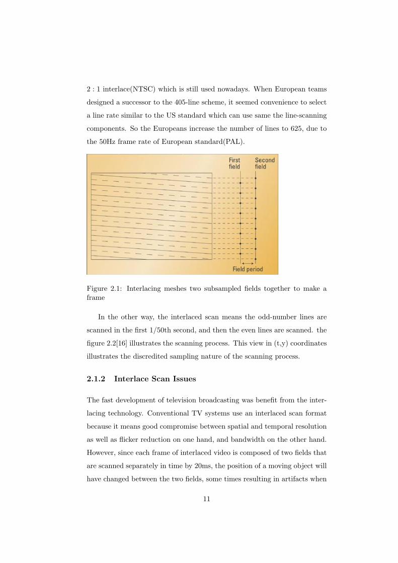
2 : 1 interlace(NTSC) which is still used nowadays. When European teams
designed a successor to the 405-line scheme, it seemed convenience to select
a line rate similar to the US standard which can use same the line-scanning
components. So the Europeans increase the number of lines to 625, due to
the 50Hz frame rate of European standard(PAL).
Figure 2.1: Interlacing meshes two subsampled fields together to make aframe
In the other way, the interlaced scan means the odd-number lines are
scanned in the first 1/50th second, and then the even lines are scanned. the
figure 2.2[16] illustrates the scanning process. This view in (t,y) coordinates
illustrates the discredited sampling nature of the scanning process.
2.1.2 Interlace Scan Issues
The fast development of television broadcasting was benefit from the inter-
lacing technology. Conventional TV systems use an interlaced scan format
because it means good compromise between spatial and temporal resolution
as well as flicker reduction on one hand, and bandwidth on the other hand.
However, since each frame of interlaced video is composed of two fields that
are scanned separately in time by 20ms, the position of a moving object will
have changed between the two fields, some times resulting in artifacts when
11

Figure 2.2: Interlace Scan
two fields are combined to the final image.
An other problem is the development of display technology, a lot of
display devices, other than CRT, can not support the interlace scanning
format but must draw the screen each time. The video must be de-interlaced
before it can be displayed. De-interlacing requires the display to buffer one
or more fields and recombine them into a single frame. In theory this would
be as simple as capturing one field and combining it with the next field to be
received, producing a single frame. But also due to the short time difference
between two continuous fields, the de-interlace results in a “tearing” effect
where alternate lines are slightly displaced from each other. Modern de-
interlacing systems therefore buffer several fields and use techniques like
edge detection in an attempt to find the motion between the fields. This is
then used to interpolate the missing lines from the original field, reducing
the ”tearing” effect [17].
Due to problems mentioned above, from the 1940s onward, improvements
in technology allowed the US and the rest of Europe to adopt systems using
12

progressively more bandwidth to scan higher line counts, and achieve better
pictures. However the fundamentals of interlaced scanning were at the heart
of all of these systems.
2.1.3 Progressive Scan
Compared with interlace scan, the other method of scanning –progressive
scan means all lines of a video frame are scanned successively and each field
has the same number of lines as a frame. The scan lines in a progressive
image are scanned from one row to the next, from top to bottom. The whole
frame is created in one time, which is different from interlace scan.
Compared with the interlace scan, the progressive scan has a higher ver-
tical resolution under the same frame rate.(Vertical resolution: the number
of rows, dots or lines from top to bottom on a printed page, display screen
or fixed area such as one inch. Contrast with ”horizontal resolution,” which
is the number of elements, dots or columns from left to right.) It offers
fewer artifacts than interlace scan. The main drawback compared with the
interlace scan is that it requires higher bandwidth than interlaced video that
has the same frame size and vertical refresh rate.
2.2 Two Interlacing Modes
For compatibility reasons, the NTSC/PAL scanning scheme has been carried
over to the digital camera employing the CCDs/CMOS image sensor which
can record the video. The first work using interlacing technology in CCDs is
introduced by Carlo in 1973 [18]. From then on the interlaced CCD cameras
was becoming popular. Why is the artifacts disadvantage not simple avoided
by switching to a progressive scan? There are 2 reasons for this. One
reason is more about economy: extensive modification in the construction
of the broadcasting system. This involves a major effort and considerable
expenses. Many users would outweigh the advantages. The other reason
13
is for interlaced scan the sensor could have better light sensitivity than
progressive scan sensors. To better understanding this advantage we will
introduce the two different modes of interlacing scan.
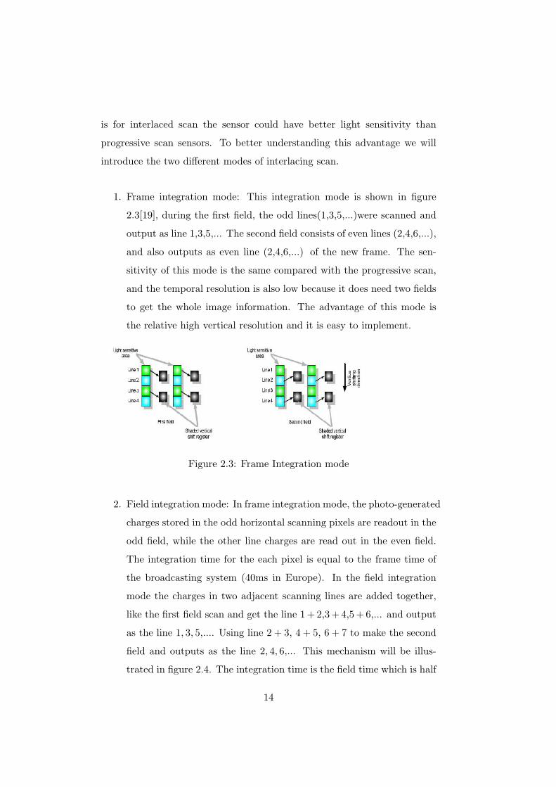
1. Frame integration mode: This integration mode is shown in figure
2.3[19], during the first field, the odd lines(1,3,5,...)were scanned and
output as line 1,3,5,... The second field consists of even lines (2,4,6,...),
and also outputs as even line (2,4,6,...) of the new frame. The sen-
sitivity of this mode is the same compared with the progressive scan,
and the temporal resolution is also low because it does need two fields
to get the whole image information. The advantage of this mode is
the relative high vertical resolution and it is easy to implement.
Figure 2.3: Frame Integration mode
2. Field integration mode: In frame integration mode, the photo-generated
charges stored in the odd horizontal scanning pixels are readout in the
odd field, while the other line charges are read out in the even field.
The integration time for the each pixel is equal to the frame time of
the broadcasting system (40ms in Europe). In the field integration
mode the charges in two adjacent scanning lines are added together,
like the first field scan and get the line 1 + 2,3 + 4,5 + 6,... and output
as the line 1, 3, 5,.... Using line 2 + 3, 4 + 5, 6 + 7 to make the second
field and outputs as the line 2, 4, 6,... This mechanism will be illus-
trated in figure 2.4. The integration time is the field time which is half
14

of the frame time (20ms in Europe). The characteristics of field inte-
gration mode of scanning can be concluded as below. First, no field
time lag [20]. Due to the lower integration time for field integration
mode, charges for the preceding field remain in the photo-diode(called
“field time lag”) is much less than frame integration mode. Secondly,
reducing the flicker at vertical edges of image. The field integration
mode doubles the vertical aperture. Thirdly, the vertical resolution of
the field is lower than progressive scan and frame integration mode.
And last but not least, it has a high sensitivity, wide dynamic range
compared to the frame integration mode. The field integration mode
combines two scanning lines together, which is equal to enlarges the
pixel size two times and means better the light sensitivity and dy-
namic range [21]. The design of this thesis is also based on the field
integration mode due to its high sensitivity.
Figure 2.4: Field Integration mode
2.3 CMOS Image Sensor Pixel Circuits
2.3.1 Photodiode
A photosensitive element is the indispensable part of an image sensor. The
basis of photosensitive imaging is the photo-electric effect [22]. When a
semiconductor is exposed to light, the incident photons will penetrate into
the material generating electron-hole pairs, as long as the incident photons
15

have energy higher than the bandgap of the semiconductor. In the solid-state
imaging, the most widely used semiconductor material is silicon, which has
a bandgap low enough (1.1eV) to allow visible light to generate electron-hole
pairs.
Figure 2.5: Photocurrent Generation in P-N junction
In order to detect the generated electron-hole pairs, a quick separation
the electrons from the holes is necessary to stop the recombination. The
simplest method is using a reversed pn junction as a photodiode structure
(figure 2.5). The electric field across the depletion region will cause the
electrons to drift towards the n-doped region, the holes drift towards the p-
doped region. In a word, when a photodiode is exposed to light, the incident
light will produce electron-hole pairs that results in a reverse current, often
called photocurrent. To accurately measure the photocurrent, all modern
solid state imagers work in integrating mode. The photocurrent is integrated
onto a capacitance, and the voltage change across the capacitance is read
out.
16

2.3.2 Photodiode Three Transistor (3T) Pixel
Normally, we classify CMOS Image Sensor according to their pixel struc-
tures. These pixel structures can be classified into two catalogs, which is
named the passive pixel sensors(PPSs) and the active pixel sensors(APSs).
PPSs structure consists of a photodiode and a select transistor as shown
in figure 2.6[23]. When the access transistor is “on”, the photodiode is con-
nected to a vertical column bus. A charge integrating amplifier readout
circuit is arranged at the bottom of the column bus. This pixel is charac-
terized by a large fill factor. The fill factor indicates the size of the light
sensitive photodiode relative to the total area of the pixel.
Figure 2.6: Passive Pixel Structure
To improve the PPSs structure, the APSs design was proposed. The
APS pixel inserts an amplifier within every pixel.Since each amplifier is
17

only active during its readout, the power dissipation is minimal. The most
common type of the APS is the photodiode three transistor (3T) pixel as
figure 2.7 shows. In the schematic below we can see the source follower is
the amplifier in the pixel, the two other transistors in pixel are used for
addressing (RS), and reset the pixel(RST). The potential of the photodiode
is to reset to the highest voltage value through a reset transistor (RST = 1),
after reset, the photon generated charges are collected and converted to a
voltage by the photodiode. After the integration time, the voltage video
signal is sensed by the source follower. When particular row was selected
(RS = 1), the row select transistor operates in the triode/linear region as
an analog selection switch. Then the video signal can be accessed on the
column bus. The pixel is reset again afterward.
Figure 2.7: Photodiode 3T Pixel
Compared to APSs pixel structure, PPSs has the advantages like high fill
factor, high quantum efficiency, and a simple structure. The disadvantages
18

Figure 2.8: Timing of 3T APS pixel
are mainly because its readout noise level and scalability. The passive pixel
also does not scale well to larger array sizes and or faster pixel readout rates.
This is because increased bus capacitance and faster readout speed both
results in higher readout noise. The photodiode capacitance is very small
compared to the large vertical column and horizontal bus capacitance. This
mismatch in capacitances results in a large noise component added to the
signal during readout of the photodiodes. To solve the problem the active
pixel inserted a buffer/amplifier into the pixel could potentially isolate the
sense node from the column capacitance and improve the performance of
pixel. Adding an amplifier to each pixel significantly increases sensor speed
and improves its SNR, thus overcoming the shortcomings of PPS. Decrease
in detector area is compensated by an increase in conversion gain. The
conversion gain (2.1) reveals the relationship between the voltage output of
the pixel and the number of electrons stored on the photodiode, which is
determined by the photodiode capacitance in 3T APS pixel.
CF = (q
CPD×ASF ) (2.1)
CPD : photodiode capacitance;
ASF : gain of source follower;
But 3T APSs still have their own problems. Introducing an amplifier within
every pixel increases the mismatch between the different pixels. If uncor-
rected, this mismatch will cause large offsets which is called Fixed Pattern
Noise. Fixed Pattern Noise (FPN) is also one of the main disadvantages
of CMOS imagers compared with CCD technology. Canceling FPN can be
performed by on-chip or off-chip storage of the offset values while the pixel is
19

reset. Double sampling (DS) is an effective way to implement this cancela-
tion. During the pixel readout cycle, two samples are taken. One when the
pixel is still in the reset state and the other when the video signal (and noise)
has been transferred to the read-out node. Although DS reduced the fixed
pattern noise to a large extent, for 3T APS, DS will increase the reset noise
(KT/C noise) in the 3T APS pixel. The double sampling operation, the re-
set signal sampling and integration signal sampling, needs to be completed
within a short readout time (RS = 1). Thus, the integration signal which
contain both the reset noise and the video signal will be sampling at the
end of integration period. The reset signal which mainly contains the reset
noise will be sampling at the beginning of the next integration period. Since
the reset signal in the two samples (two different integration periods) are
not correlated with each other, the double sampling, which means subtract
between two signals, will make the reset noise increased but not canceled
out.
2.3.3 Pinned Photodiode Four Transistor (4T)Pixel
Pinned Photodiode 4T pixel, as the mainstream choice of CMOS image
sensor nowadays, as shown in figure 2.9 [23] introduces two elements. One
is the regular photodiode is replaced by a pinned photodiodePPD. The
other is a transfer gate TX is added between PPD and the floating diffusion
node. The common purpose of these two elements is to establish charge
transfer from the photodiode. As can be seen in band diagram 2.10 [24],
the sandwich structure (p-n-p) of PPD can store the charge underneath
the surface and into the silicon. An other goal of adding a transfer gate
TX is to decouple the PPD region from the sense node and to split two
important conversions – photon to charge conversion and charge to voltage
conversion. When the transfer gate TX is turned off, the pinned photodiode
is insulated from the readout FD node, thus the integration of the photo-
generated charge happens at the capacitance CPD of the the photodiode. If
20

Figure 2.9: The 4T Pinned Photodiode Pixel
Figure 2.10: Band diagram comparison of two photodiodes
21

the transfer gate TX is turned on, the accumulated charge is transferred to
capacitance CFD of the floating diffusion node, and the charge is converted
into voltage signal. This separation makes two parameters, the full-well
capacity and the conversion gain not highly related anymore. In 3T APS,
the way to improve conversion gain is decrease the CPD which will also
deteriorate the full-well capacity at same time. After the decoupling in 4T
PPD, the conversion gain is related to the CFD, the full well capacity is
related to the CPD. Thus, compared with a 3T pixel, the conversion gain
of 4T pixels is normally higher, which is attractive when obtaining high
light sensitivity. On the hand, photon to charge conversion and charge to
voltage conversion decoupling also means that read and reset operations can
departed with integration period. Thus, correlated double sampling(CDS),
as will be discussed in detail in section 2.4.2, can be used in a 4T imager
design. Compared with 3T non-correlated double sampling, as explained
before, the kTC noise can be eliminated completely in 4T PPD pixel. These
aspects are clarified by the timing diagram.
The rest of the pixel components perform the same function as in 3T APS
design: reset transistor, source follower, and row select transistor. From the
Figure 2.11: Timing diagram of 4T Pinned Photodiode Pixel
timing diagram in figure 2.11 and presents the sequences for three control
signals:“RS”, “RST” and “TX”, we can know the working principle of 4T
pinned photodiode pixel.
22

1. When a particular row is addressed, the correspondence “RS” signal
of this row is “on”, the readout voltage is accessible on the column
bus(Col).
2. Within the line time, the “RST” pulse reset the voltage of the float-
ing diffusion node to the highest voltage value which cleans all the
charges left in the sense node. At this time the transfer gate TX is
turned off and the signal charge generated by incident light is collected
on the photodiode capacitance CPD. But after reset, the floating dif-
fusion node still has some noise charges which were produced by the
kT/C/reset noise during the reset operation. After the reset pulse is
made low, a first sample is taken. This sample contains the kT/C
noise generated with the reset of the floating diffusion as well as offset
and 1/f noise of the source follower transistor.
3. After the first sampling, the transfer gate “TX” is pulsed. The photo
generated charges were transferred from the pinned photodiode to the
floating diffusion. After this transfer is finished, the second sample is
taken, which contain the signal, KTC noise from the floating diffusion,
offset and 1/f noise from the source follower.
As mentioned before, the pinned photodiode 4T can quickly transfer the
charge to diffusion node, which allows the reset of the floating diffusion to
be performed before reading the signal, and the two samplings performed in
the same integration period. Thus, the kT/C noise generated with the reset
is correlated between the two subsequent samples, and it will be canceled
out together with offset and 1/f noise of source follower by subtracting the
two samples.
The significantly lower noise level of 4T pixels compared to the read-
out operation with 3T pixel structures make pinned photodiode 4T pixels
become the mainstream choice of CMOS image sensor.
23

2.4 Increasing Signal-to-Noise Ratio in CMOS Im-age Sensor
From the first chapter, the signal-to-noise ratio is defined as equation 1.2.
To improve the signal noise ratio, the challenge can be stated as more signal
with less noise. In this section, first, the main noise sources in CMOS 4T
pixel are analyzed. Secondly, the important noise cancelation mechanism
Correlated Double Sampling technology will be introduced in detail. Then
the binning technology will be present, which can significantly enhance the
signal level.
2.4.1 Overview of Main Noise Sources in CMOS 4T Pixel
The noise sources in our image sensor can be classified into 3 categories:
input-signal noise, spatial noise, temporal noise sources.
Photon Shot Noise
Photon Shot Noise is an important input-signal noise, which relates to fun-
damental physical laws, rather than circuit design and technology. Photon
shot noise is caused by a statistical phenomenon following a Poisson distribu-
tion which is resulting from the random variation of the number of discrete
electrons generated and captured by the sensor. It is basically due to the
quantum nature of light, photon shot noise can not be separated from the
signal. Because it appears before any signal processing or output operation,
even before the detection.
The photon shot noise is equal to the square root of the mean number
of electrons generated by photons like the figure 2.12 [25] shows. From
the square relationship of the photon shot noise, doubling the photons will
increase the noise by√
2, the signal-to-noise ratio still can increase 3dB.
SNR = 20 log(Nsig/nshot) = 20 log(Nsig/√Nsig) = 10 logNsig(dB) (2.2)
24

Figure 2.12: The relationship of photon shot noise and collected photon
Nsig = V oltage of the video signal;
nshot = V oltage of the photon shot noise;
Therefore, under the limits of the photon shot noise, designers will try to
increase the photon-generated electrons under a given level of illumination
to improve the performance. With the constrains of the fill factor and pixel
pitch, light intensity, and the exposure time, the charge domain interlacing
technology in field integration domain is a efficient way to enhance pho-
ton generated electrons. The other solution could be increase the quantum
efficiency of the photodiode.
Reset/kTC Noise
As mentioned in the section 2.3, the “reset” operation in the APS pixel will
lead to a kTC or reset noise which is an important temporal noise source.
When a capacitor is charged through a resistor, the uncertainty of the charge
25

Figure 2.13: kTC noise
stored on the capacitor causes the kTC noise. The figure 2.13 shows the kTC
noise model. And from this model we can conclude following formula.
Z =R
(1 + j2πfRC)
Re(Z) =R
(1 + (2πfRC)2)
Vt = [∫ ∞
04KT
R
1 + (2πfRC)2df ]
12 =
√kT
C
Qres = C × U =√kTC
(2.3)
From the formula listed above we can conclude that if we want to reduce
the kTC noise then the capacitor of the floating diffusion in the pixel should
be small, because the noise in the floating diffusion is in the charge domain.
The capacitor in CDS sample and hold circuit should be large due to the
fact that the signal and noise already are converted in the voltage domain.
Fixed Pattern Noise
Fixed pattern noise(FPN) is a classic spatial noise and it can be divided into
dark and light fixed pattern noise. Dark FPN noise is mainly caused by non-
uniformities of dark current generation. Light FPN is mainly caused by non-
26

uniformities of pixel or column response. Therefore, the noise is not related
to the fluctuations of the time domain, but affected by the distribution in
spatial domain.
The non-uniformity is caused by the offset of the source follower in dif-
ferent pixels which can be decreased by CDS as we already mentioned in
last section.
Others
Except the noise sources discussed before, there still are a lot of noise sources
like thermal noise, 1/f noise. These two noises are generated inside the MOS
transistors and these two noises are common in a lot of analog circuits.
σR =√
4KTR ·BW (2.4)
Thermal noise is well known as “white” noise, or Johnson noise. It caused by
the random thermal motion of the charge carriers in the conductor. Accord-
ing to the formula 2.4, the thermal noise is mainly determined by absolute
temperature and noise bandwidth. Therefore, the reduction method for the
thermal noise is to reduce the temperature and the bandwidth. In addition,
instead of reducing thermal noise in CDS, thermal noise will be increase
under the implementation of the CDS mechanism. Because the two thermal
noises of reset and signal samples are not correlated with each other. When
two noise is not correlated, then the subtraction between two samples will
get N2 = N12 +N22.
1/f noise is also an important noise source, which is dominant in the
source follower transistor of APS pixel. Revealed by McWhorter [26] in
1955, 1/f noise is mainly caused by lattice defects at the interface of the
Si − SiO2 channel of the MOS transistor. The random current variation
raised by these defects trapping and de-trapping the conducting carries is
1/f noise. On one hand, increasing the size of source follower transistor can
highly reduce the 1/f noise; on the other hand, the area inside the pixel
27

is highly limited and it will also affect the fill factor significantly. Thus,
increasing transistor size to decrease the noise is not practical at all. In
addition, 1/f noise is technology-dependent and just can be fully canceled
out under some special conditions using CDS. In conclusion, 1/f noise is
hard to be fully eliminated.
The analog signals produced by the light-sensitive elements are apt to
be contaminated by the noises mentioned above, causing the lower sensitiv-
ity or lower dynamic range of CMOS image sensor, compared to the CCD
technology.
2.4.2 Correlated Double Sampling Technology
In previous analysis, Correlated Double Sampling(CDS) technology has been
mentioned a lot of times. CDS is a very useful signal processing method for
CMOS image sensors. It substrates the reset level from the signal level to
suppress the noise. In this subsection we would like to explain CDS in detail.
CDS technology is based on the sample/track and hold circuits. Track-and-
hold circuits consist of a switch and a capacitor as shown in figure 2.14.
A capacitor is used to store the analog voltage, and the switch is used to
control the connection between input signal and capacitor. When the switch
is “on”, the output signal will track the input signal; when “off”, the output
signal is insulated with input change, the voltage on the capacitor will be
hold until next track phase begins. This holding allows more processing
to be done to the output signal. In most system, Track and Hold circuit
produce the time-discrete samples from the time continuous input. But for
the CDS of a CMOS image sensor, the input of the CDS readout circuit is
already time-discrete. In the figure 2.15, we can show the working principle
of CDS technology.
The input of the CDS can be classified into 3 phases. 1)The sensitive
node was reset to a predetermined value. 2) A ”zero-signal“Vr was sampled
28
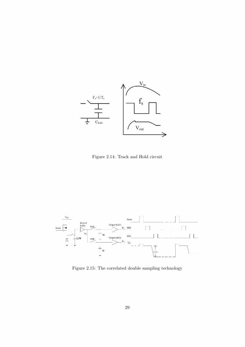
Figure 2.14: Track and Hold circuit
Figure 2.15: The correlated double sampling technology
29

by SHR, and stored Vr on a capacitors Cr and 3)The transfer gate is open,
the charge accumulated in the specific integration time was transferred to
CFD. Then SHS trigger the sampling process, the sampled voltage Vs is
stored on the signal capacitor Cs for the readout. The resetting of the sensi-
tive node introduces a number of unwanted noise components: kT/C noise,
1/f noise components, etc. The correlated double sampling technology elim-
inates a number of these components by first sampling the ”zero-signal”level,
then together with the sample from the signal sample period, and subtract
these two samples with each other. The transfer function for the unwanted
noise components is:
|H (w)| = |2sin (wTd/2)| = |2sin (ΠfTd)| (2.5)
Td is the delay between the two sample moments. From the transfer
function (2.5)[27] we know that CDS acts as a high pass filter and shows
a great suppression to low frequency noise. On the other hand, the noise
at higher frequencies is increased. The circuit implementation of the CDS
technology will be discussed in next chapter.
Except decreasing noise components like mentioned above in this sec-
tion, improving the signal-to-noise ratio of the CMOS image sensor, can
also be done by increasing the signal. Charge-domain binning technology
is an effective way to increase the signal level specially in low light level
application. It will be introduced in detail in next section.
2.5 Charge Domain Interlacing Pixel Design forHigh Sensitivity CMOS Image Sensor
Improvement of sensitivity or dynamic range becomes a critical challenge
of CMOS image sensor design, this section intends to present some special
pixel design arrangements to increase pixel sensitivity and to improve the
overall image quality.
30

In this section we first introduce the charge binning technology. Then
based on this technology and combined with the interlace scan to improve
the performance of the CMOS image sensor, this project propose two dif-
ferent pixel structures.
2.5.1 Binning Techniques Increase Signal-to-Noise Ratio inCMOS Image Sensor
The binning technology in the charge domain is based on the idea from shar-
ing the readout circuitry among pixels. In 2004, Matshushita [28] and Canon
[29] both presented shared readout circuit pixels. The concept of sharing the
readout circuit by 4 pixels is time-division multiplex readout. In rolling shut-
ter or global shutter mode, at one time, just have one pixel was readout by
one amplifier. But the readout structure in pixels can be shared by different
photo-sense elements. In figure 2.16, we can see four photodiodes controlled
by 4 separate transfer gates, and shared one common floating diffusion which
accepts the transferred charge with single readout circuit(“reset” transistor,
source follower, and row selector). Thus, 7 transistors are required to read-
out 4 pixels, which means that only 1.75 transistor/pixel is necessary. These
shared readout structure pixels were intended to produce small pixels with
a high fill factor.
2.5.2 Two Photodiodes Shared Amplifier Structure
Inspired by this shared amplifier structure and combined with the field in-
tegration mode, we can add the readout of neighboring lines in the charge
domain through special pixel design. It allows the charge from multiple pix-
els to be measured in a single read operation, reducing the total noise in the
final image and increasing the sensitivity of the sensor when it is operated
in this mode. In field integration mode, each row will be scanned twice(both
odd field and even field), not only the readout structure will be shared by
two photodiodes placed in two rows, but also the individual photodiodes
31
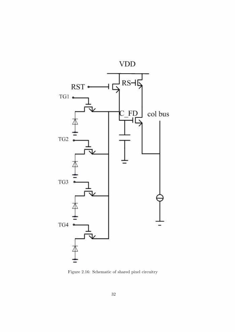
Figure 2.16: Schematic of shared pixel circuitry
32

will be connected and readout by two neighboring readout structures.
Figure 2.17 contains two graphs. (A) is the normal arrangement of the
pixel column. This arrangement can only realize the progressive scan and
this 4T pinned photodiode structure has 4 transistor/pixel. (B) is the de-
signed pixel which has the vertical two photodiode shared amplifier struc-
ture. Every photodiode controlled by two transfer gates TX. For example,
photodiode 2 was connected to T2〈0〉 and T2〈1〉 separately. It can realize
both the interlacing scan in field integration mode and progressive scan.
1. With progressive scan and display, every photodiode was readout by
corresponding readout structure in turn. photodiode“1” was readout
by first source follower and get the output at “1′”; “2”was readout at
“2′”, “3”was readout at“3
′”...
2. When this design was used in an interlace scan application with re-
peated scan of the same photodiode row for both odd and even fields.
In addition, the neighboring photodiode are sensed in combination.
In the odd field scan, charges accumulated in “1”and “2” are trans-
ferred to one common floating diffusion by turning on T10 and T20 at
same time. The corresponding output voltage“1′”is the combination
of the signal produced by “1” and“2”(“1′”=“1”+“2”), which signifi-
cantly enhances the sensitivity of the pixel by a factor of roughly two
as compared with progressive scan in figure 2.17(A). The scanning se-
quence is photodiode(1,2),(3,4),(5,6)(7,8),...by driving transfer gates
TXs on turn (T1〈0〉, T2〈0〉), (T1〈2〉, T2〈2〉), (T1〈4〉, T2〈4〉),... and get-
ting the readout signal in odd rows like “1′”, “3
′”, “5
′”, “7
′”... In
the even field, the photodiode(2,3), (4,5), (6,7),... combination was
readout by turning on the transfer gates in turn like (T1〈1〉, T2〈1〉),
(T1〈3〉, T2〈3〉), (T1〈5〉, T2〈5〉), (T1〈7〉, T2〈7〉)...The output gives the even
rows like “2′”, “4
′”, “6
′”,... The detail timing diagram can be seen in
figure 2.18
33

Figure 2.17: (A):Normal CMOS image column (B): Vertical two photodiodesshared amplifier structure
34

Figure 2.18: Timing Diagram of Vertical two photodiode shared amplifierstructure
35

This structure adds one more transfer gate per pixel which achieves 5 tran-
sistor/pixel(photodiode), so the fill factor is lower than a 4T pixel. The
advantage of this structure is the two signals(for example:signal produced
by photodiode in Row 1 and Row 2) are combined in charge domain at
the front end but not in the voltage domain or digital domain like tradi-
tional interlace. For instance, two real signals S1, S2, with total noises in
two photon sense element like the dark current noise and photon shot noise
which produced in the photon-charge conversion as Nc1, Nc2, the signal we
get in the common floating diffusion will be S1 + S2 + Nc1 + Nc2. For this
shared readout structure, adding the noise like reset noise, 1/f noise which
produced in the pixel readout phase just Nr, the total readout signal is
Stotal1 = S1 + S2 +Nc1 +Nc2 +Nr. If we combine the signal after the read-
out in the voltage domain, the combination of signal after readout could be
Stotal2 = S1 +S2 +Nc1 +Nc2 +Nr1 +Nr2 which has much more severe noise
contamination than Stotal1, even if we do not consider the Fixed Pattern
Noise produced by mismatch.
The other special arrangement of the two shared pixel design is shown
in figure2.19. The characteristic of this arrangement is a different readout
direction for the odd and the even field. In the odd field scan, the signal
output(1′, 3
′, 5
′, ...) was read at column (x, x + 1, x + 2...).In the even field
scan, the signal output(2′, 4
′, 6
′, ...) was read at column (x − 1, x, x + 1...).
One particular column line is shared by pixels both left and right, both odd
and even field. Due to the interlacing scan, there will be an vertical offset
between odd and even fields, but this can be compensated in the read out
chain.
2.5.3 Three Photodiodes Shared Amplifier Structure
Base on the same idea of two photodiodes shared amplifier structure and in
order to improve the fill factor of two photodiodes shared amplifier struc-
ture, a three photodiodes shared readout structure is presented here [30].
36
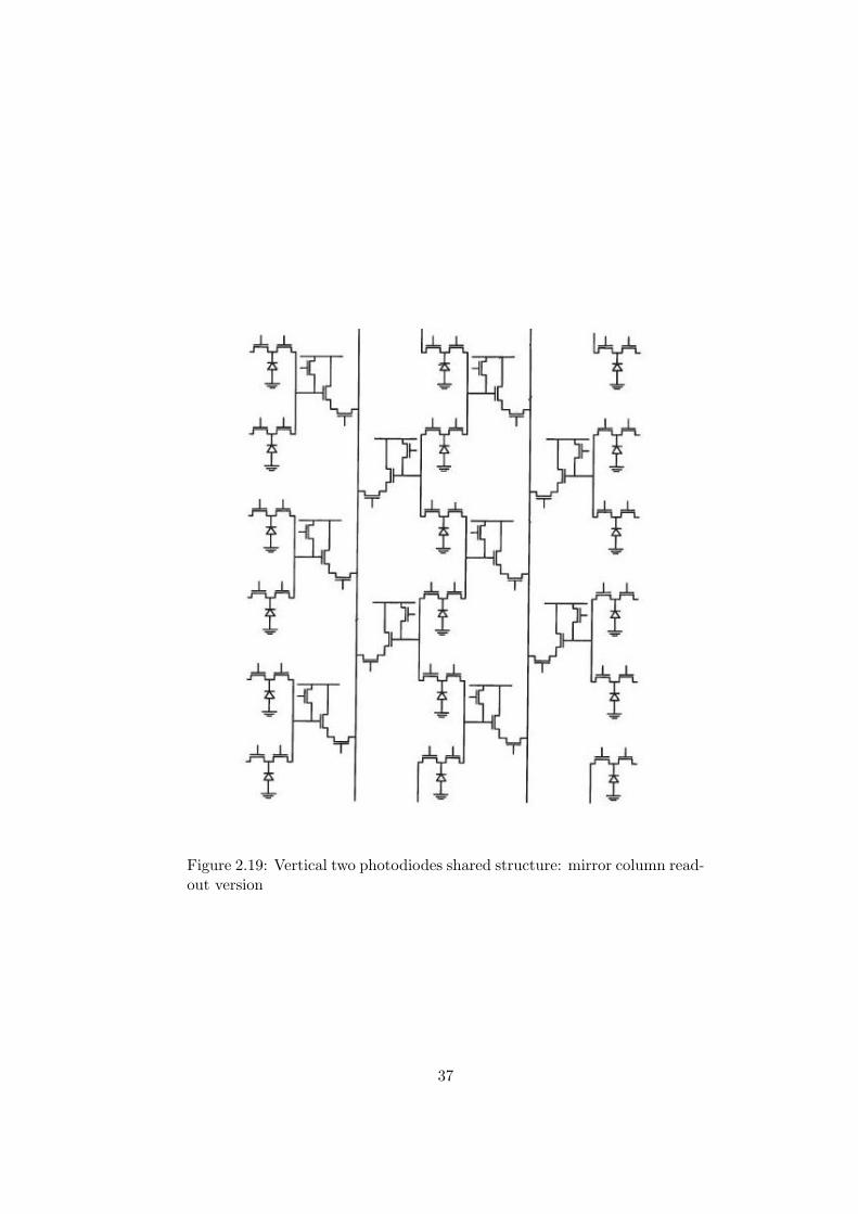
Figure 2.19: Vertical two photodiodes shared structure: mirror column read-out version
37

This structure also can be used in both progressive and interlace scan. The
difference is it reuses the readout structure in odd and even field. The
schematic of this pixel design is shown in figure 2.20. For this structure, ev-
ery odd number photon sense element(like photodiode1,3,5,7...) is connected
with two transfer gates like photodiode 3 was connected to transfer gates
T2〈0〉, T1〈1〉. All of the transfer gates T2 are use in even field scan. And all
T1 are used in transfer charges in odd field scan. These two transfer gates
belong to two readout circuits respectively. The even numbered photon sense
elements (like photodiode 2,4,6...) are not shared but belong to one partic-
ular pixel readout circuit no matter in the odd field scan or even field scan.
The photodiodes connected with transfer gates T2〈n〉(n = row number),
which will turn on not only when T1〈n〉 = 1 in odd field scan; but also
T2〈n〉 = 1 in even field scan.
The working principle of this structure for interlace scan were:
1. When the odd field time begins, transfer gate pairs turn on in sequence
like (T1〈0〉, T3〈0〉), (T1〈1〉, T3〈1〉), (T1〈2〉, T3〈2〉)..., the output in the
odd field gets “1′”=“1”+“2”, “3
′”=“3”+“4”, “5
′”=“5”+“6”...
2. When the even field time begins, activated transfer gates pairs change
to (T2〈0〉, T3〈0〉), (T2〈1〉, T3〈1〉), (T2〈2〉, T3〈2〉)...Using the same read-
out circuit as for the odd field scan, the output was changed to “2′”=“2”+“3”,
“4′”=“4”+“5”, “6
′”=“6”+“7”... Because this structure reuses the
readout circuit in the two fields, the number of readout circuits will
be reduced to the half. Considering the extra transfer gate, this struc-
ture could improve the fill factor significantly and achieve 3 transis-
tors/pixel(photodiode) which is lower than normal 4T pixel.
The disadvantage of this three photodiode shared amplifier structure is
about the mismatch. It is hard to layout three photodiodes connected to
one readout amplifier exactly the same with each other. This will cause the
mismatch between pixels and produce fixed pattern noise.
38

Figure 2.20: Vertical three photodiodes shared amplifier structure
39

In addition, all of these shared amplifier structures use the common
floating diffusion which will be larger than normal 4T APS pixel. This means
the associated capacitance CFD will be larger and reduce the conversion
gain. The other problem caused by large CFD is its effect for kTC noise,
however it can be eliminated by CDS.
2.6 Chapter Summary
In this chapter, based on the understanding of the interlace scan principle,
the introduction of basic 4T APS structure, and analyzing the origins of the
main noise sources in pixel, we propose some charge domain interlace pixel
structures to enhance the signal-to-noise ratio and light sensitivity, which
can improve the overall image performance.
40

Chapter 3
Sensor Architecture
In the last chapter, the working principle of a charge domain interlacing
CMOS image sensor is explained. In this chapter, the circuit level imple-
mentation of the charge domain image sensor will be introduced into detail.
In section 3.1, an overall architecture of this test chip will be presented. In
the following, from section 3.2 to section 3.6 the sensor design will be divided
into different functional blocks to be discuss individually. In the section 3.7,
the overview of the designed sensor will be concluded.
3.1 Architecture of the Charge Domain Interlac-ing Image Sensor
The figure 3.1 is the whole architecture of the sensor, which contains several
parts. I will introduced them as follow:
Pixel Array: the light sensitive part of the image sensor. It contain
96× 128 pixels, converting the light signal into a voltage signal.
Current Source Array: a current source is needed on every column bus.
The current source is used to bias the source follower in the pixel and charge
the parasitic capacitor of each column.
Column Multiplexer: according to the even or the odd field to select the
column bus processed by the column analog chain.
41

Figure 3.1: Architecture of charge domain interlacing CMOS image sensor
42

Column readout circuit: implementing the CDS (correlated double sam-
pling) and analog signal processing chain to readout the column bus and
output the processing signal.
Row Driver Array: decoding the gray code row address and providing
driving signals for the specific addressing pixel row.
Column Driver Array: when a specific row is addressed by the row driver
array(decoded from the row address), the column driver array will decode
the gray code to drive the column readout circuit column by column.
Programmer Pulse Generator: buffers the series input signals and use
different clock domain transfers from the series input signals to the parallel
control signals. These control signals contain the row addressing signals, the
pixel control signals, the column bus readout control signals and so on.
Gray Code Counter: when the counter is triggered, 7 bits gray address
code is produced with the rising edge of the CLK. This code will be used to
address and readout the column readout circuits.
Output buffer: the output stage of the sensor, buffers the analog output
signal to enhance the driving capability of the sensor output.
3.2 Pixel Array
3.2.1 Pixel Design
The pixel array contains two type of pixel designs which are introduced
in the chapter 2. And both two pixel designs can be organized into two
different readout directions. For figure 3.2, from row 0 to row 62, there is
the two photodiode shared amplifier structure pixel. From row 63 to row
94, there is the three photodiode shared amplifier structure pixel. From the
Column line 0 to Column line 48, these pixels use the mirror column readout
direction structure to readout.
As mentioned in last chapter and shown in figure 3.3, a basic cell of
43

Figure 3.2: Pixel Array of Sensor
44
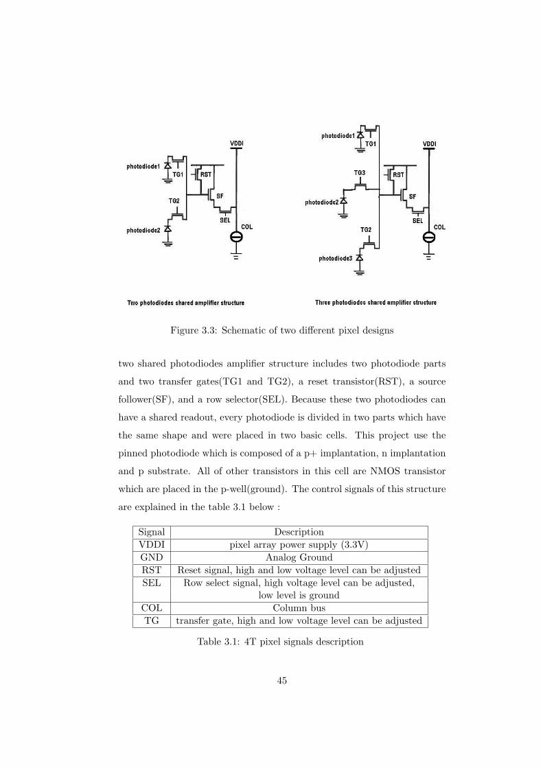
Figure 3.3: Schematic of two different pixel designs
two shared photodiodes amplifier structure includes two photodiode parts
and two transfer gates(TG1 and TG2), a reset transistor(RST), a source
follower(SF), and a row selector(SEL). Because these two photodiodes can
have a shared readout, every photodiode is divided in two parts which have
the same shape and were placed in two basic cells. This project use the
pinned photodiode which is composed of a p+ implantation, n implantation
and p substrate. All of other transistors in this cell are NMOS transistor
which are placed in the p-well(ground). The control signals of this structure
are explained in the table 3.1 below :
Signal DescriptionVDDI pixel array power supply (3.3V)GND Analog GroundRST Reset signal, high and low voltage level can be adjustedSEL Row select signal, high voltage level can be adjusted,
low level is groundCOL Column busTG transfer gate, high and low voltage level can be adjusted
Table 3.1: 4T pixel signals description
45

3.2.2 Layout Considerations
Figure 3.4 and Figure 3.5 are layouts of the basic cell of two photodiodes,
and three photodiodes shared amplifier structure respectively. The basic
cell of “two photodiodes shared amplifier structure” contains two photodiode
parts, but one is just the half of the actual photodiode size. The pitch of this
structure is 10um×10um. The fill factor of this pixel design is 46.37%. The
other type “three shared photodiodes amplifier” structure contains one more
photodiode and one more transfer gate. Because this three shared structure
is used in both even and odd field, and contains one independent photodiode
and 2 shared photodiodes, the area of this basic cell is 20um×10um. The fill
factor of this structure pixel is 47.8% which improves the fill factor compared
with two photodiode shared amplifier structure. As shown in figure 3.4, the
big red area is the pinned-photodiode part. Along every photodiode there
is a blue rectangular structure which is the transfer gate of the 4T pixel
structure. The readout structure is located in the middle of structure, which
makes two photodiodes having the same distance to the readout structure.
The three transistors in readout structure is reset transistor(RST), source
follower transistor(SF), row select transistor(RS).
In this particular project, the pixel design should consider two aspects,
first of all, symmetric requirement. These pixels are used in charge domain
interlacing design. Some photodiodes will be shared by different readout
circuits and charges stored in the photodiode will be transferred in two dif-
ferent directions. Even for column 0 to column 48, the readout direction is
different in neighboring rows. Thus, the two photodiodes share one readout
circuit should be fully symmetric with respect to the readout structure of
the pixel. For the three photodiode shared amplifier structure(figure 3.5),
the photodiode 2 is just being readout by one readout circuit, and controlled
by one transfer gate. But the other two photodiodes 1 and 3 are shared in-
dividually by two readout structures in neighboring rows and controlled by
46

two transfer gates. In this situation, the layouts of the three photodiode
are hard to be exactly the same to each other. But if we just consider the
charge domain interlacing scan mode, the output signal is from the integra-
tion voltage of charges produced by photodiode 1 and 2 together, or charge
produced by photodiode 2 and 3 together. No matter which combination,
the photodiode 2 is always included. Considering the photodiode 1 and 2
together as a readout unit, photodiode 2 and 3 together as a readout unit,
these two units should be symmetric.
To control the transfer gate for photodiode2, there is a metal line con-
nected with TG3 of all the pixels in one particular row. In order to keep
the metal away from the photodiode, we just could connect this TG3 at one
end of the gate TG3. But for the symmetry of the layout and to avoid the
non-even electrical potential across the gate of TG3, a second metal TG3
should be added to balance the electrical potential in the poly of TG3.
Second, to reduce the kTC noise, the capacitance of the floating diffusion
should be small, specially for this project, the floating diffusion of two or
three photodiode connected together for one readout circuit, which will be
larger than normal design. In this situation, the layout should try to control
the area of the floating diffusion to reduce the kTC noise.
3.3 Current Source Array
3.3.1 Column Current Source Design
From the pixel operation, we know that a current source is necessary for each
column bus. The current column source Icol is not required continuously
during an imaging cycle, but only when the pixel values require to be reset
for integration and readout. On one hand, the column current source is
used to bias the source follower of pixel. On the other hand, for every pixel
connected in one column bus, the row select transistor introduces a parasitic
capacitor to the column bus, the column current source was used to charge
47

Figure 3.4: Layout of the two photodiodes shared amplifier basic cell
48
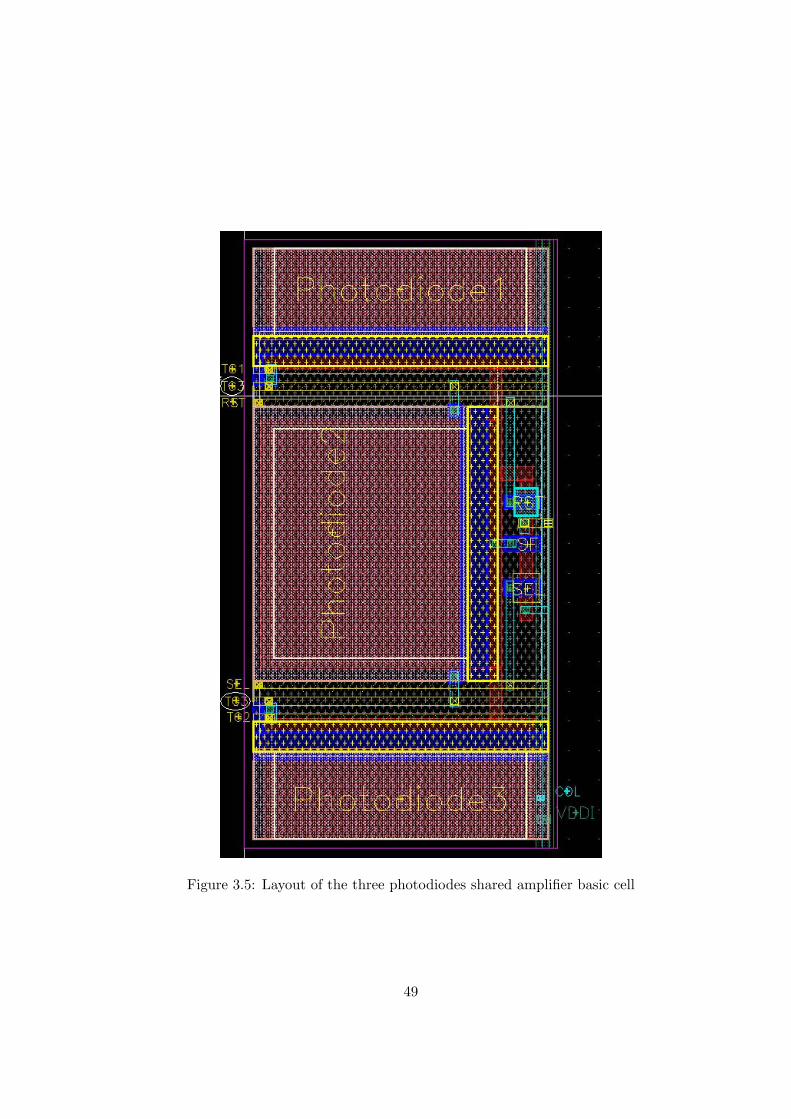
Figure 3.5: Layout of the three photodiodes shared amplifier basic cell
49

or discharge these capacitors to the stable value.
The figure 3.6 shows the circuit of one column current source. It can be
divided into two parts according to the function. The first part is the current
source (M5 and M9). Saturated PMOS transistor M9 and NMOS M5 is
operated as current sources. The source ends of two transistor are connected
together, which could improve the Power-Supply Rejection Ratio(PSRR) to
reduce the influence of the jitter from power and ground. A stable current
reference for current mirror can be provide by this structure. The second
part is the current mirror (M3 and M4). The same W/L ratio of M3 and M4
makes the current Id(M3) mirroring the Id(M4) which is equal to 12uA. The
last part M2 and M11 are used to allocate the current value for column bus.
When CS = 2.7V , the NMOS M2 is “on”, nearly the total output current
of M3 is concentrated to Icol(Id(M2)). When CS= 1.4V, the total current is
flow into the PMOS transistor M11, the NMOS M2 is turn “off”. When the
CS is adjusted in between, the column current can be changed between 0 to
12uA. Thus, based on this current source circuit, the current ratio of PMOS
and NMOS can be relocated easily, then the column current value can be
controlled by input bias. But combined with the control mechanism, in this
sensor, CS just can choose 2.7V or 1.4V by the digital control signal NSEL.
This limitation can be improved in the future design to give more choices
for column current.
VDDI pixel array power supply (3.3V)gnd Analog Ground
Biasn Bias voltage produce by Biasing Part(3.3V)Biasp Bias voltage produce by Biasing Part(855mV)
CS switch of the col current which is controlled by one ofthe input control signal(NSEL) of the sensor. When digital signalNSEL=“1”(1.8V), CS=2.7V; when NSEL=“0”(ground), CS=1.4V
COL Corresponding column bus
Table 3.2: Current source signal description
50

Figure 3.6: Schematic of column current sensor
3.3.2 Design Considerations
To design of the column current source is a tradeoff between the speed of
the pixels and the noise performance. From the speed consideration, the
large column current results in a the fast speed for charging and discharging
the parasitic capacitance. From the noise consideration, a large current
also means a large gm of the source follower, and means a large thermal
noise contribution to the output signal. So a compromise between these two
aspects is made for the column current.
The design of the column current source is critical because the trans-
fer gain of the in-pixel source follower is sensitive to this column current
source. Even the small variation on the current value would change the
source follower gain, which is one of origins of the non-linearity of the pixel.
This current source structure is repeated in every column, so the layout
of the current source in each column must fits the pixel pitch 10um.
51

Output buffer Bus_rst<n>
Out_en<n>
SHS
SHR
Cs
Cr
ReadS<n>
col<n>
ReadR<n>
RST
SEL
TG
VDD3v3
GND
Cload
Figure 3.7: Column signal processing chain
3.4 Column Readout Circuit
Since the pixel array design and the current source array design are intro-
duced in last two sections, we can get the signal and reset voltage from the
column bus. To implement the CDS technology and get the output signals
of the whole pixel array with good driving capability and correct timing
sequence, an signal processing chain is needed for every column bus. Figure
3.7 is the schematic of the whole signal processing chain for one column,
which shows the whole course from light input to the sensor analog output.
This signal processing chain can be divided into two parts, the sample and
hold(S/H), the readout timing control, and the output buffer.
3.4.1 Sample-hold and Readout Circuit
This part will describe how to sample and hold the output signals and read-
out for every column bus when a particular pixel row is addressed. As figure
3.7 shows, every column bus has two 1pf capacitors (Cs and Cr) which are
used to store the reset level and the signal level respectively. The timing
diagram of control signals of the column readout circuit is shown in figure
3.8.
1. When a row is addressed, all of the pixel output signals in that row
52

Line timeSEL
RST
TG
SHR
Line<n> Line <n+1>
SHS
ReadR<0>
col_rst<0>
ReadS<0>
Out_en<0>
ReadR<1>
col_rst<1>
ReadS<1>
Out_en<1>
Figure 3.8: Timing diagram of 4T pixel and CDS readout
53
should be sampled and stored in Cs or Cr at the same time. Thus,
the sample signal SHS and SHR are global signals for all the column
readouts. When the row select signal SEL is high, that row is ad-
dressed. Then after the reset, the reset levels of all pixels in that row
are sampled and stored in corresponding column Cr by SHR = 1; af-
ter charges which are accumulated in the photodiode were transferred
to the floating diffusion(TG = 1), the signal levels of all pixels are
sampled and stored in the corresponding Cs by SHS = 1. Until now,
signals of all columns are stored in their corresponding capacitor.
2. After sample and hold the signal in capacitors Cr and Cs, readout
circuits will be driving one by one from column 0 to column 96 and
finished one row readout in one line time. For instance, when driv-
ing column readout circuit of column〈0〉, switches of ReadR〈0〉 and
output enable(out en) will open to transfer the stored reset signal to
the output bus. Then the bus was reset by col rst〈0〉 = 1. After the
reset(col rst〈0〉 = 0), the video signal stored in the Cs〈0〉 will be trans-
ferred to output bus (ReadS〈0〉 = 1&out en〈0〉 = 1). When both reset
signal and video signal were readout, the output bus will reset again
by col rst〈0〉 = 1. Finished the readout of column line 0, the column
line 1, 2,... will be readout at the same principle until the last column
line 96. It is important to notice that the necessary subtraction of the
two signals to complete the CDS action is done off-chip.
3. Then the next row is addressed, the readout process depicted in 1 and
2 will be repeated again until the whole pixel array was scanned.
These readout control signals are listed in the table 3.3 below.
For this particular application, some columns (from column line 0 to
column line 48) have different readout directions for odd and even fields.
For example column line 〈1〉 is not only connected the odd field output of
the first column, but is also connected with the even field output of the
54

field_en
col<0> col<1> col<2> col<47> col<48>
Column readout circuit <0>
Column readout circuit <1>
Column readout circuit <2>
Column readout circuit <n>
Column readout circuit <47>
Figure 3.9: Principle of column multiplexer
Signal Type Sensitivity DescriptionSHS input active high Global sample signal for the Signal level.
High is 3.3V, low is groundSHR input active high Global sample signal for Reset level.
High is 3.3V, low is groundReadR〈n〉 input active high Readout switch for the reset signal
from Cr of the column. High is 3.3V , low is groundReadS〈n〉 input active high Readout switch for the video
signal from Cs of the column. High is 3.3V, low is groundcol rst〈n〉 input active high Reset pulse for the column readout bus.
If col rst = 1, then the readout bus was reset.High is 1.8V, low is ground
out en〈n〉 input active low Output enable signal, when reset signalor video signal were readout in column n, then
out en〈n〉 = “0′′. High is 3.3V, low is analog groundfield en input level field en = 1 means odd field scan,
and field en = 1 means even field scan
Table 3.3: Column Readout Control Signals
55

second column. Then, to process these readout signal, the column bus will
be selected by different column signal processing chains. In figure 3.9 we
can see the field en signal to select a field. When the scan field is the odd
field(field en = 1), the output direction of these pixels is the right, the 2
to 1 multiplexer will choose the column line 〈1〉 for column readout circuit
〈0〉, column line 〈2〉 for column readout circuit 〈1〉... When the scan field
is the even field(field en = 0), the output direction changes to the left.
The 2 to 1 multiplexer will choose the column line 〈0〉 to be processed by
column readout circuit〈0〉, choose column line 〈1〉 to be processed by readout
circuit〈1〉, and so on.
3.4.2 Output Buffer
The output stage of the sensor should satisfy a number of special require-
ments. One of the most important is to minimize the output impedance
so that the output voltage will not be affected by the load impedance. An
analog buffer which has a low output resistance, high driving capability can
satisfy the requirement. Another requirement for the output stage in this
sensor is the wide dynamic range. In this project, a CMOS buffer with a
wide dynamic range and a capacitive load driving capability is needed. This
buffer is connected to the output of all 96 column readout circuits which
can buffer and delivery the reset signal and video signal of column 1 to col-
umn 96 in turn. This amplifier will use a differential pair with an active
current mirror structure and implement as a unity gain feedback topology.
In figure 3.10, the M0 and M2 are identical, M3,M1 are identical too. The
input range of output buffer should tolerate the reset signal and the min-
imum video signal. The minimum input voltage for this buffer is equal to
VDS4 + VGS3,min, and the maximum allowable input voltage will put input
transistor M3 at the edge of the triode region which is
56

Figure 3.10: Schematic of output buffer
57

Vin − Vth = VG3 = V DD3v3− |VGS3|
Vin,max = V DD3v3− |VGS3|+ Vth
(3.1)
Suppose Vth is about 0.7V in this technology, and the overdriver VGS −
Vth = 0.3V . Then Vin,max = 3.3−1+0.7 = 3V , and Vin,min = 0.3+0.3+0.7 =
1.3V . From the simulation of the analog chain, we can know the reset voltage
is around 2.7V. And the maximum pixel voltage swing was estimated to be
1V. Then the minimum video signal we get is about 2.7− 1 = 1.7V , which
is higher than the minimum voltage of the buffer. So this buffer design is
enough for this application.
Another concern about the buffer is the settling time. From transient
simulation we can see the step response of the amplifier in figure 3.11. And
if we define the error less than -50dB (0.3% accuracy), then the settling
time is 81.3ns. In this project, the pixel clock for one column readout is
416kHz, and sample frequency of off chip ADC is about 800kHz, which is
about the two times of the pixel clock. This settling time could satisfy the
requirements of this application. From the AC response of the close loop
amplifier 3.12, we can see the united gain bandwidth is about 10MHz, which
is far beyond the requirement of the output stage.
Figure 3.11: Buffer settling time with the accuracy
58

Figure 3.12: Close loop AC response of buffer
3.5 Row and Column Driver
In this part, the row and column driver design will be introduced. There
are two basic functions for the row driver and column driver. One is the
addressing and decoder. The other one is according the decoding signal
to produce driving signals for the target row or column. The structure of
the column and row driver are shown in figure 3.13. These row and column
drivers are basically digital circuits. Normally, they can be easily designed in
hardware description language and automatically generated by CAD tools.
In the image sensor design, the row and column driver should fit the pixel
pitch which is 10um for the column and row driver(some of the row drivers
should fit the 20um due to the three photodiode shared amplifier structure).
No software tools can do the layout fitting to the pixel pitch. Then the
column and row driver should be designed and layout at gate level.
3.5.1 Gray Code Addressing
In this project, we use a Gray code as the address signal to addressing
the column or row. The Gray Code is unweighed and is not an arithmetic
59

Row Driver<0>
Row Driver<1>
Gray Decoder
Row Driver<94>
Row Driver<n>
7 bIts Gray Cod
(Row address)
RST<1>SEL<1>TG1<1>TG2<1>
RST<0>SEL<0>TG1<0>TG2<0>
RST<n>SEL<n>TG1<n>TG2<n>
RST<94>SEL<94>TG1<94>TG2<94>TG3<94>
Row
Driver<96>
Gray
Decoder
Colum
n Driver<0>
Colum
n Driver <n>
7 bIts Gray Code
(Column address)
Figure 3.13: Structure of Column and Row Driver
code which means there are no specific weights assigned to the bit positions.
It is a cyclic binary code, and specifically designed for position information
[31]. A gray code sequence is a set of numbers represented as combination of
digits “1” and “0” in which contiguous numbers have only one bit difference.
Inspired by this characteristic of the Gray code, we use a switchable two
way bus to deal with the addressing problem. The metal 3 was used to
transmit the invert state of the address code, and metal 2 was used to
transmit the address code. And the bit state will invert by exchanging the
metal 2 and metal 3 with each other. Figure 3.14 depicted a 5 bits Gray
code bus example. From this example we can see the lowest bit D〈0〉 of
the Gray code convert its state in every two column/rows, and the D〈1〉
converts state in every four columns/rows. With increasing bit position, the
conversion frequency is decreased by a factor of two. In reality, the column
and row bus are 7 bits and for every column driver, a 7 bits address signal is
connected to a 7-input NAND. For example, if we want addressing the row
No. 10, the gray code address is 0001111. After the transition in the bus line,
the address will becoming 1111111 at the corresponding column driver. The
60

NAND in the addressed row driver will output a falling edge as the decode
signal . The other NAND for non-addressed columns drivers will still be
“1”. When the load row address is 1111111, then without any transition in
this switchable address bus, the row 128 was addressed. The decoder part
D<0>
D<1>
D<2>
D<3>
D<4>
Figure 3.14: 5 bits gray code bus
in both row and column driver are the same Gray code addressing bus with
7-input NAND corresponding to every column/row. But for row addressing,
the row address signal is produced by FPGA on the PCB, then the driving
sequence for the row is flexible. For column addressing, the column address
is produced by a Gray code counter in the sensor. This gray counter can be
reset by the input control signal. If the reset signal is not active, the counter
will keep counting to produce the column address in turn.
3.5.2 Row and Column Driver Array
A row driver is necessary for every pixel row. For a 4T pixel, signal like
“RST 〈n〉”, “TGs〈n〉” and “SEL〈n〉” are generated by row driver 〈n〉 ac-
cording to the decode signal. The figure 3.15 above is the schematic of the
row driver. When address present in 7-input NAND is 1111111, then this
row is addressed. The following table 3.4 describes the input signal behav-
61

SELn
RSTn
TG1n
TG1Gn
Voltageshift
Voltageshift
Voltageshift
Voltageshift
SEL<n><0><1><2><3><4><5><6>
TG1<n>
TG2<n>
RES<n> TG2Gn
Vresel_H GNDA
TG_H TG_L
TG_H TG_L
Vresel_H Vresel_L
Figure 3.15: Schematic of Row Driver
Signal Type Sensitivity DescriptionSELn input active low The row select pulse, which can produce a row select
signal for the selected 4T pixel row, the signalcomes from the programmable pulse generator.
RSTn input active low The reset pulse, which can produce RST signalfor the selected 4T pixel row, this signal comes
from the programmable pulse generator.TG1n input active low The transfer gate pulse which will produce
TG1 signal for the selected pixel row.TG2n input active low This is the transfer gate pulse
which will produce TG2 signal for the selected pixel row.TG1Gn input active low This is the global signal for the transfer gate pulse
produced by programmable pulse generator. When thissignal is active, then TG1 of all rows will be open.
TG2Gn input active low This is the global signal for the transfer gate pulseproduced by programmable pulse generator. When this
signal is active, then TG2 of all rows will be open.Vresel H input n.a High voltage for pixel reset (RST)
and row select (SEL) signal.Vresel L input n.a Low voltage for reset signal (RST)TG H input n.a High voltage for transfer gate (TG1/TG2)TG L input n.a Low voltage for transfer gate (TG1/TG2)
Table 3.4: Row driver input signals
62
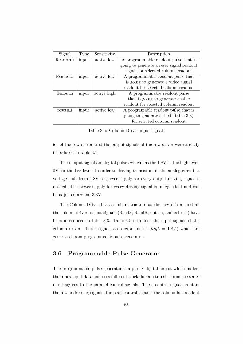
Signal Type Sensitivity DescriptionReadRn i input active low A programmable readout pulse that is
going to generate a reset signal readoutsignal for selected column readout
ReadSn i input active low A programmable readout pulse thatis going to generate a video signal
readout for selected column readoutEn out i input active high A programmable readout pulse
that is going to generate enablereadout for selected column readout
resetn i input active low A programable readout pulse that isgoing to generate col rst (table 3.3)
for selected column readout
Table 3.5: Column Driver input signals
ior of the row driver, and the output signals of the row driver were already
introduced in table 3.1.
These input signal are digital pulses which has the 1.8V as the high level,
0V for the low level. In order to driving transistors in the analog circuit, a
voltage shift from 1.8V to power supply for every output driving signal is
needed. The power supply for every driving signal is independent and can
be adjusted around 3.3V.
The Column Driver has a similar structure as the row driver, and all
the column driver output signals (ReadS, ReadR, out en, and col rst ) have
been introduced in table 3.3. Table 3.5 introduce the input signals of the
column driver. These signals are digital pulses (high = 1.8V ) which are
generated from programmable pulse generator.
3.6 Programmable Pulse Generator
The programmable pulse generator is a purely digital circuit which buffers
the series input data and uses different clock domain transfer from the series
input signals to the parallel control signals. These control signals contain
the row addressing signals, the pixel control signals, the column bus readout
63

control signals and so on.
First, DATA CLK is 24 times of the frequency of the pixel clock(CLK).
Then DATA CLK can shift 11 bits valid DATA IN in the last 11 DATA CLK
pulses of one pixel CLK cycle. In one pixel CLK can write one 7 bit register.
These are eight different 7 bit registers to generate the different control
signals. In this 11 bits data, the first 4 bits are the address for addressing
the target register. The next 7 bits represent the data we want to write into
the register. The timing diagrams of the DATA IN, CLK, and DATA CLK
are shown in the figure 3.16. DATA IN is the only control signal input
pad for the sensor. DATA CLK is the data clock to write into the register.
CLK is the main clock for the pixel readout. At the rising edge of the
DATA CLK, the DATA IN were shifted into the register, because of the
limited depth of the input register, only during the last 11 cycles, DATA IN
will be written into the register. In this example, a bitstream “01111000000”
was shifted into sensor. Then we can know the first 4 bits are referring to
the address“1110”, then reg11〈6 : 0〉 was write into “0000001”. The detailed
allocation of the register will be explained in table 3.6.
Figure 3.16: Timing Diagram of Sensor Input
The programmable value of Reg1 was related to the timing of setting the
ReadR signal. The programmable value of Reg4 was related to the timing
of resetting the ReadR signal. And the programmable value of Reg7 was
related to the timing of resetting the ReadS signal. Reg 11 was related to
set the ReadS signal. Out en and col rst are also related to these timing
sequence.
64

For 7 bit register 11 − 13, nearly every bit in these registers are con-
nected with the corresponding control signal. In this way, through program
different value to register 11− 13, we can change states of these control sig-
nal to produce the right timing for sensor work. The table 3.7 listed detail
information about these registers.
Register Address contentReg1 0001 SR resetReg4 0110 SR setReg7 0100 SS resetReg10 1111 SS setReg11 1110 pulse registerReg12 1010 pulse registerReg13 1011 pulse registerReg14 1001 row address
Table 3.6: Register Allocation
Register Connected signal DescriptionReg11〈0〉 resetoff If resetoff = 1, then col rst signal for
the column readout reset is not active anymore.Reg11〈5〉 NSEL If NSEL = 1, then current source switch onReg11〈6〉 SSHn If SSHn = 0, then column address gray code
counter is reset to 0Reg12〈0〉 SELLALLn If SELLALLn = 0, all rows are addressed togetherReg12〈1〉 SHRReg12〈2〉 SHSReg12〈3〉 odd sel If field en = 1, then means odd field scan,
otherwise means the even field scanReg12〈6 : 4〉 TG3Gn
TG2Gn, and TG1GnReg13〈4 : 2〉 TG1n,
TG2n, and TG3nReg13〈5〉 ROWnReg13〈6〉 RESn
Table 3.7: Pulse Generation Registers
65
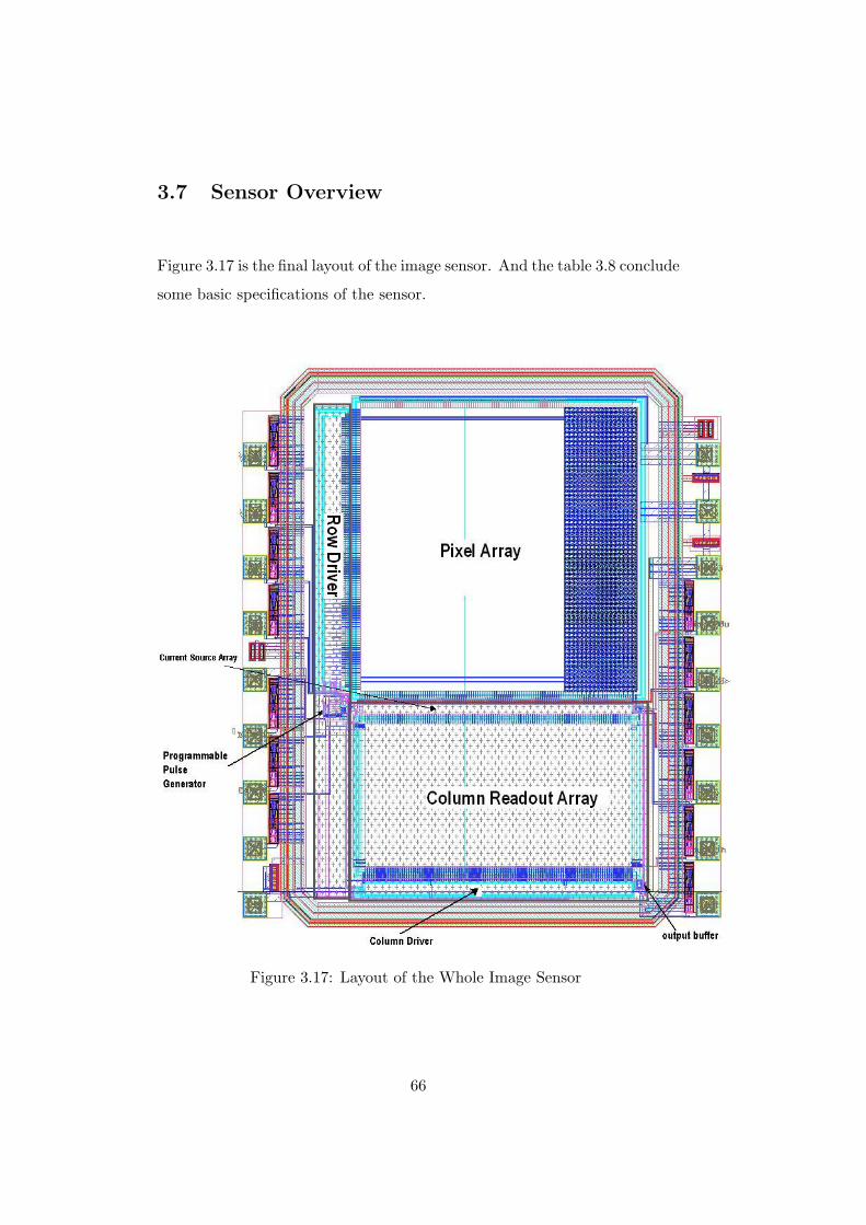
3.7 Sensor Overview
Figure 3.17 is the final layout of the image sensor. And the table 3.8 conclude
some basic specifications of the sensor.
Figure 3.17: Layout of the Whole Image Sensor
66

Technology TSMC 0.18um CMOS Image SensorMixed Signal Technology
Die size 2.3mm× 2.7mmSupply voltage 1.8V/3.3V
Pixel type 4T APSPixel Pitch 10umPixel Array 96× 128
Clock Frequency 416 kHz
Table 3.8: Sensor Overview
3.8 Conclusion
In this chapter, the architecture and working principle of an universal image
sensor test chip with a charge domain interlacing pixel design are introduced
and implemented in silicon. From section 3.2 to section 3.6, the individual
blocks of the sensor both of the analog part(pixel array, current source, col-
umn readout circuit, and output buffer) and of the digital part (row and
column driver arrays, programmable pulse generator) are presented respec-
tively.
In the next chapter, the basic measurement result of the testchip and
PCB level setup will be given. The basic function ability of the test chip is
proved by test result.
67

68

Chapter 4
Initial Measurement Results
This chapter focus on the measurements of the designed sensor. The mea-
surement set-up will firstly be described, then the most important part, the
initial measurement results, will be presented, as well as the analysis and
discussion of the results.
4.1 Measurement Setup
The setup of the measurement can be found in Fig 4.1, where the under-
test image sensor is placed on the designed printed circuit board(PCB). The
PCB is connected to the computer to process the digital image signal. On
the oscilloscope we can also see the waveform of the sensor analog output.
It can directly help us to know whether sensor is working normally. To
better understand the measurement setup, the IO pins of designed chip are
described in table 4.1.
The measurement PCB is mainly composed by under-test sensor, FPGA,
ADC, frame grabber, quarts crystal, and power supply system. The FPGA is
the central control part of the PCB. First of all, it generates the suitable pixel
clock, data clock, and data-in for the image sensor. Changing the driving
sequence and working mode of the sensor will be very flexible by changing
the programmable input data sequence. Secondly, the FPGA supplies the
69

Under Test Image Sensor
Power Supply
+6 -6
ADC
FPGA
Analog output
GND
OscilloscopeFrame
Grabber
PC
lightDigital Signal
Processing&
Display
Programmer
Figure 4.1: Measurement setup for the sensor
Pin name Type DescriptionDATA CLK Input clock Clock for writing series data into register(10MHz)DATA IN Digital input Programmable data input of sensor
CLK Input clock pixel clock, in one clock period,one pixel was readout(416.6kHz)
Aout analog output the analog output include the reset and video signalVDD3V3 power supply main power for analog circuit(3.3V)GNDA ground analog groundVDDI power supply adjusted pixel array voltage(3.3V)TG L power supply adjusted low voltage for transfer gate (0V)TG H power supply adjusted high voltage for transfer gate(3.3V)
Vresel H power supply adjusted high voltage of Vg(3.3V )for pixel reset and row select transistor
Vresel L power supply adjusted low voltage of Vg
for pixel reset transistor(0V)VSS ground digital groundVDD power supply main power for digital circuit (1.8V)
Test pads test output reserving 5 test pads for important biasingsignals, middle stage output signal and so on
Table 4.1: IO pins of the designed image sensor
70
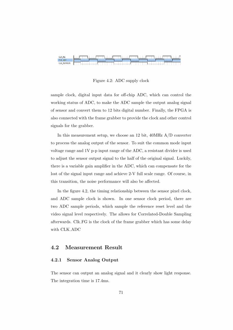
Figure 4.2: ADC supply clock
sample clock, digital input data for off-chip ADC, which can control the
working status of ADC, to make the ADC sample the output analog signal
of sensor and convert them to 12 bits digital number. Finally, the FPGA is
also connected with the frame grabber to provide the clock and other control
signals for the grabber.
In this measurement setup, we choose an 12 bit, 40MHz A/D converter
to process the analog output of the sensor. To suit the common mode input
voltage range and 1V p-p input range of the ADC, a resistant divider is used
to adjust the sensor output signal to the half of the original signal. Luckily,
there is a variable gain amplifier in the ADC, which can compensate for the
lost of the signal input range and achieve 2-V full scale range. Of course, in
this transition, the noise performance will also be affected.
In the figure 4.2, the timing relationship between the sensor pixel clock,
and ADC sample clock is shown. In one sensor clock period, there are
two ADC sample periods, which sample the reference reset level and the
video signal level respectively. The allows for Correlated-Double Sampling
afterwards. Clk FG is the clock of the frame grabber which has some delay
with CLK ADC
4.2 Measurement Result
4.2.1 Sensor Analog Output
The sensor can output an analog signal and it clearly show light response.
The integration time is 17.4ms.
71

Figure 4.3: Two photodiodes shared amplifier structure readout with stronglight intensity(TG1 = high;TG2 = high)
1. Basic light response: to measure the image senor, the basic thing is to
test the light response of the sensor. The pixels in the fifth row are
readout as example. Figure 4.3 and figure 4.4 are “two photodiodes
shared-amplifier structure” output under strong light condition and
low light condition in respectively. The two transfer gates TG1〈5〉,
and TG2〈5〉 which are connected to the two photodiode are opened
together. Because we did not complete CDS technology fully on chip,
here we can see the both the reset level and the video signal level.
Cursor1 indicates the pixel reset level, and cursor2 indicates the pixel
signal level.
From the figure 4.3 we can see Vrst = 2.78V , Vsig = 1.16V . After
substraction, the real signal across these two photodiodes is Vrst −
Vsig = 1.62V (nearly saturated). In figure 4.4 we can see Vrst = 2.78V ,
Vsig = 2.64V . The real signal in this low light situation is Vrst−Vsig =
0.14V . From the figure above we can clearly see the light response.
2. Charge binning response for two photodiodes shared-amplifier struc-
72

Figure 4.4: Two photodiodes shared amplifier structure readout with lowlight intensity(TG1 = high;TG2 = high)
ture: in chapter 2, the charge binning technology is introduced, and
based on this technology, this thesis proposed two pixel structures to
enlarge the signal level. Figure 3.3 in chapter 3 shows the two pixel
structures we proposed. Here we will compared the pixel response
of the normal one pixelRow5 readout with the charge binning of two
photodiodes in one ”two photodiode shared-amplifier structure” in fig-
ure 4.5. In the interlace scan, if TG1 and TG2 open together, then
electrons accumulated in photodiode 1 and photodiode 2 will be trans-
ferred into one floating diffusion and then be readout. Here, the read-
out signal under a certain light level is Vrst−Vsig = 2.80−2.44 = 0.36V .
If with the same light level, just TG1 is open, TG2 is closed, then only
the electrons accumulated in photodiode1 will be readout. The read-
out signal is Vrst − Vsig = 2.80 − 2.64 = 0.16V . Compared these two
results we can see charge binnning can clearly increase the signal level.
In this situation, the difference of these two is 0.2V.
3. Charge binning response for three photodiodes shared amplify struc-
73

Figure 4.5: Charge binning comparison for two photodiodes shared-amplifierstructure readout under the same light intensity
Figure 4.6: Charge binning comparison for three photodiodes shared-amplifier structure readout under same light intensity.
ture: the measurement result (Pixel in Row 66) for the other pixel
design “three photodiodes shared amplify structure” shown in the fig-
ure 4.6. It also shows two waveforms. One is for the charge binning
condition when both of TG3 and TG1 (figure3.3) open together, the
signal be readout is Vrst − Vsig = 2.80− 2.58 = 0.22V . The other one
is with only TG3 open to readout electrons in the photodiode 2, the
signal we get is Vrst − Vsig = 2.80 − 2.7 = 1.0.1V . The difference of
TG1 open or not is 0.12V which is similar with the last measurement
for “two photodiodes shared-amplifier structure”.
74

It should be clear that the light conditions for these two pixel structure
measurements is different. So it can not compared these two pixel structures
from data above.
4.2.2 image result
In this subsection, the image result we get will be shown here. The figure
4.7 is image we get from the progressive scan.Because of the rotation of
the figure, the top part is the three photodiodes shared amplifier structure.
The bottom part of the image uses the two photodiodes shared amplifier
structure.
The figure 4.8 is the mickeymouse image get from the interlace scan
in the field integration mode. The top one is the even field scan, and the
bottom one is the odd field scan.
Compared these two figures, we can see the signal level in the background
of figure 4.8 is clearly has more light than figure 4.7. But in reality, these
image are get from the same illumination condition. This reveals that the
charge domain interlacing principle can enhance the signal level in certain
degree.
4.3 Conclusion
With the very first measurement results of the designed sensor, it has been
shown that sensor is working and the proposed pixel structures can truly
enhance the signal level to a certain degree. The detailed performance mea-
surement and analysis will be done in the future.
75

Figure 4.7: Image result of progressive scan
76

Figure 4.8: Image result of interlace scan
77

78

Chapter 5
Conclusion and Future Work
5.1 Conclusion
CMOS image sensors suffer from several noise sources which will affect the
image performance especially under low illumination. To improve the overall
quality of the image, a high S/N ratio and wide dynamic range are desired.
To improve the S/N ratio, a lot of work has been done to reduce many
kinds of noise sources. It can be done by using correlated double sampling
technology to cancel the reset noise and the transistor offset and so on.
Reducing the noise also can be done by improve the technology and the
device to reduce the noise sources at their origins. But improving the S/N
ratio can also be achieved by enhancing the signal level under the same light
condition.
Inspired by the field integration mode of the interlaced scan, we can
add the signal of neighboring rows signal together and using the interlace
mode to achieve a the high signal level under the same light conditions. To
realize this mechanism, the easiest way is to add the pixel readout signal in
voltage domain or even in the digital domain. But for an image sensor a
lot of noise sources are coming from the readout course of the pixel. If the
readout signal is added in the voltage domain, this will increase the noise
level of the output stage which can not achieve the purpose of improving
79

the S/N ratio. To deal with this problem, this thesis proposes two different
pixel structures based on 4T APS structure and both of them can combine
the collected charges of two pixels and then readout them together.
The first pixel structure uses one pixel readout structure connected to
two photodiodes, by using one floating diffusion to combine the photon-
generated electrons from two pixels together and then readout this com-
bined signal. From the photodiode standpoint, each photodiode is connected
with two readout structures and two transfer gates which are active in the
even field scan and odd field scan respectively. The other pixel design uses
one pixel readout structure connected to three photodiodes. Both of these
structures can realize the charge domain interlacing principle to enhance the
signal level from the front end of the sensor.
To test these pixel designs and the working principle, a programmable
universal image sensor driving circuit architecture was proposed, which can
driving and readout the pixel array flexible and easily change it through
different programming. This sensor can not only support progressive scan,
frame integration interlace scan mode,voltage domain field integration inter-
lace scan mode, but also can realize the charge domain interlacing principle
with some special pixel designs.
The designed image sensor is implemented in TSMC 0.18um process,
and the first measurement result were given. Further testing results are
expected after September 2009.
5.2 Future Work
Due to the limited time, only preliminary measurement results are included
in this thesis, more measurements will be performed later in order to give
further details about the performance analysis especially with respect to
the noise aspects. On the other hands, better understanding the principle
is important as well. More measurement need to be done to compared
80

the different pixel designs with respect their noise performance and other
aspects. It is interesting to use the different scan modes and their analysis
to look for similarities and differences between the measurement results and
theoretical model.
81

82

Bibliography
[1] S.Morrison. A new type of photosensitive junction device. Solid-State
Electronics, 6,issue 5:485–494, 1963.
[2] J.Horton et al. The scanistor-a solid-state image scanner. Proceeding
of IEEE, 52:1513–1528, 1964.
[3] M.A.Schuster et al. A monolithic mosaic of photon sensors for solid
state imaging applications. IEEE Transactions on Electron Devices,
ED-13:907–912, 1966.
[4] G.P.Weckler. Operation of p-n junction photodetectors in a photon flux
integration mode. IEEE Journal of Solid-State Circuits, SC-2, 1967.
[5] P.Nobel. Self-scanned silicon image detector arrays. IEEE Transactions
on Electron Devices, 14:202–209, 1968.
[6] W.S.Boyle et al. Charge-couple semiconductor devices. Bell System
Technical Journal, 49:587–593, 1970.
[7] F.Andoh et al. A 250,000-pixel for high-speed television cameras. Tech-
nical Digest ISSCC, San Francisco, US, pages 212–213, Feb. 1990.
[8] R.H.Nixon et al. 128× 128 CMOS photodiode-type active pixel sensor
with on-chip timing, control and signal chain electronics. Proceeding of
SPIE, 2415:117–123, 1995.
[9] S.Kempaineen. CMOS image sensors:eclipsing CCDs in visual informa-
tion? EDN 42(21), pages 101–102, 1997.
83
[10] M.Bigas et al. Review of CMOS image sensors. Microelectronics Jour-
nal, pages 433–451, 2006.
[11] A.J.P.Theuwissen. Solid State Imaging with Charge-Coupled Devices.
Kluwer Academic Press, Boston, 1995.
[12] M.Mase et al. J.Park. A 142db dynamic range cmos image sensor with
multiple exposure time signals. A-SSCC Dig. Tech. Papers, pages 85–
88, Nov.2005.
[13] K.Hara H.Kubo et al. A linear-logarithmic cmos sensor with offset
calibration using an injected charge signal. ISSCC Dig.Tech Papers,
pages 354–355, Feb.2005.
[14] N.Akahane et al. A 200db dynamic range iris-less cmos image sensor
with lateral overflow integration capacitor using hybrid voltage and
current readout operation. A-SSCC Dig. Tech. Papers, pages 85–88,
Nov.2005.
[15] John.Watkinson Understanding Interlace.
http://broadcastengineering.com/news/broadcasting understanding interlace 2.
[16] John Amanatides and Don P. Mitchell. Antialiasing of interlaced video
animation. Computer Graphics, pages 77–85, 1990.
[17] De-interlacing. http://en.wikipedia.org/wiki/Deinterlacing.
[18] Carlo H. Sequin. Interlacing in charge-coupled imaging devices. IEEE
Transaction on Electron Devices, pages 535–541, June, 1973.
[19] Horst A.Mattfeldt. Digital and Interlaced: Moving for-
ward by stepping back? Allied Vision Technologies.
http://www.framos.eu/uploads/media/Allied 20Vision 20Technologies Mattfeldt 1 .pdf.
[20] Hiroaki Kotaki Yoshinori Takizawa. Field integration mode CCD color
television camera using a frequency interleaving method. IEEE Trans-
actions on Consumer Electronics, pages 358–362, August 1983.
84

[21] Farrell et al. Resolution and light sensitivity tradeoff with pixel size.
SPIE Electronic Imaging, page 211C218, 2006, Feb.
[22] A.Einstein. Uber einen die erzeugung und verwandlung des lichtes be-
treffenden hueristischen gesichtspunkt. Annalen der Physik,4th series,
Vol.17, pages 132–148, 1905.
[23] Albert Theuwissen. Course on CMOS Image Sensors, Delft University
of Technology, 2003.
[24] A.Bardoux. Review of APS technologies. Workshop Astrophysics De-
tectors, Nice, 2008.
[25] Nixon.O. High speed low light imaging escaping the shot noise limit.
http://www.photonik.de/fileadmin/pdf/fachaufsaetze/Photonik Intl 2007 030.pdf.
[26] A.L.McWhorter. 1/f noise and related surface effects in germanium.
PHD dissertation, MIT, 1955.
[27] Marcel Pelgrom. Analog-to-Digital Converter Slides, Test and Exer-
cises, page 154. 2009.
[28] M.Mori et al. 1/4-inch 2 mpixel MOS image sensor with 1.75 transis-
tors/pixel. IEEE Journal of Solid-State Circuits, vol.39, pages 2426–
2430, Dec.2004.
[29] H.Takahashi. A 3.9-um pixel pitch VGA format 10-bit digital output
CMOS image sensor with 1.5 transistor/pixel. IEEE Journal of Solid-
State Circuits, vol.39, pages 2417–2425, Dec.2004.
[30] Sywe N. Lee. Interlace Overlap Pixel Design For High Sensitivity
CMOS Image Sensors, Mar. 15,2005. United States Patent, Patent
No.US 6,867,806 B1.
[31] Absolute gray code encoder. http://www.electrocam.com/pdf/resolver/Encoder201.pdf.
85