characterization of stress and...
TRANSCRIPT

CHARACTERIZATION OF STRESS AND TOPOLOGY IN WLP
PROCESSES USING CGS INTERFEROMETRY
David M. Owen, Ph.D., Doug Anberg, Shrinivas Shetty, Warren Flack Ultratech, Inc.
3050 Zanker Road, San Jose, CA 95134 USA [email protected]
ABSTRACT Wafer Level Packaging (WLP) is a key component of the 3D Packaging roadmap. It expands low cost wafer-level processing to advanced packaging by delivering improved density, higher performance in a small form factor. Foundries and OSATs are investing rapidly in WLP. As with any new packaging application, WLP will be required to demonstrate mature yield levels for cost effective high volume manufacturing. Planarity has become one of the top yield detractors and assembling large surfaces with micron-scale features requires new manufacturing capabilities.
Using a full-wafer Coherent Gradient Sensing (CGS) interferometer it is possible to image precisely the surface of the WLP wafer, capturing the whole topography with three million pixels at a speed greater than 100 wafers per hour. This paper will discuss the application of the Superfast 3G system, the first production 3D WLP Macro Inspection System developed for volume manufacturing of patterned wafers. Its self-referencing interferometer allows the inspection to be made on any type of surface or films stack, and does not require a measurement target. By comparing the topography evolution between steps, planarity variations as well as stress can be measured and controlled. Given an established WLP process flow with a high mix of products, the inspection system enables rapid understanding of wafer level, die level and within die topography and stress challenges. In a foundry environment where the product layout (e.g. TSV, RDL, micro-bumps) and the planarity and stress specifications will vary, The system allows customized Statistical Process Control (SPC) of each individual production batch. This paper will discuss specific examples to demonstrate how planarity and stress process control can be put in place to insure that each product yields reliably. Key words: 3D Packaging, WLP, TSV stress, CGS, in-line inspection; statistical process control
INTRODUCTION 3D WLP Manufacturing Challenges There are many manufacturing challenges associated with current and proposed WLP advanced packaging technologies. Controlling stress and the associated wafer warpage in 3D WLP applications is critical for high yield levels. Wafer distortion can vary from wafer-to-wafer and lot-to-lot, and, in a foundry environment across different device-types. As a result, wafer distortion is perhaps the
most unpredictable component of WLP and its sources are least understood and characterized.
Traditional wafer warpage or distortion measurements have typically used point-by-point measurements to generate low-density maps of the wafer geometry with hundreds data points. Depending on the specific technique, a higher density map may be possible at the expense of throughput. The trade-off of point density and throughput has meant that the use of wafer distortion characterization has typically been limited to off-line process development. An alternative technique to measure wafer warpage and distortion is a full-wafer Coherent Gradient Sensing (CGS) interferometer. This technique provides high-density wafer maps (up to 3,000,000 data points) with relatively fast data acquisition (seconds per wafer), is described in the following section. The analysis of the wafer distortion data is discussed in the context of using wafer deformation data to understand the relationships between surface displacements, stress and wafer warpage.
CGS Interferometry Inspection systems for semiconductor manufacturing have been developed based on the CGS interferometer. The current generation of this system is called the Superfast 3G. This section describes some of the specific attributes of the system and the corresponding measurement approach for a typical patterned wafer.
The inspection system is based on the CGS interferometer that is a type of lateral shearing interferometer. The system features a collimated probe beam of greater than 300mm in diameter that is expanded from a relatively low power HeNe laser. The probe beam illuminates the entire wafer at once and the wafer stage does not require x/y motion in order to complete the measurement. The beam that reflects off of the wafer surface is distorted in accordance with the local height variations of the wafer. The interference is generated in a self-referencing manner when the distorted beam is steered though two parallel diffraction gratings. The self-referencing approach eliminates the need for an independent reference beam from, for example, a flat mirror and ensures excellent fringe contrast regardless of the reflectivity of the surface under investigation. The interference patterns are imaged on to a 2048x2048 CCD array.
The interferometer essentially compares the relative heights of two points on the surface that are separated by a fixed distance, � called the shearing distance. Physically, the

change in height over a fixed distance provides slope or tilt information and the fringes in a CGS interference pattern are contours of constant slope. For a given probe wavelength and grating pitch, the shearing distance scales with the distance between the two diffraction gratings. The sensitivity of the interferometer or the slope per fringe is determined by the ratio of the probe wavelength, � to the shearing distance. In order to reconstruct the shape of the surface under investigation, interference data in two orthogonal directions must be collected. Collection of the slope data in the x-direction and y-direction is achieved in parallel by two independent grating and camera sets. The slope data derived from the interference patterns is integrated numerically to generate the surface shape or topography. A schematic of the CGS interferometry measurement system is shown in Figure 1.
Figure 1: CGS interferometry module for full wafer topology measurement.
For each direction, a series of 10 phase-shifted interference patterns are collected at 45 degree increments in phase. The phase shifting is achieved by moving the gratings in the direction parallel to the shearing direction. Phase shifting provides several advantages. For patterned wafer measurement the most notable advantage is that the fringe contrast can be effectively separated from pattern contrast, which is static with phase shifting. Phase shifting along with the inherent self-referencing nature of the CGS technique results in relatively high measurement integrity on patterned wafers with widely varying nominal reflectivity. There is no need for dedicated or distinct targets, pads or other specialized features in the layout. Phase shifting interferometry is widely used in a variety of applications and additional details on its implementation and analysis are readily available [1].
The mapping of a 300mm wafer on to the 2048x2048 array results in each pixel corresponding to a square area of approximately 150 microns on the wafer surface. As a result, a 300mm wafer surface is mapped with greater than
3,000,000 data points with measurement times of a few seconds. For maximum system throughput, the 2048x2048 array results can be down-sampled to a 1024x1024 array, resulting in a square area of approximately 300 microns on the wafer surface, rendering a system throughput of greater than 100wph. The down-sampled data result in a 300mm wafer surface being mapped with approximately 800,000 data points. Note that for stress-induced wafer bending, the shortest in-plane length scale over which a substrate can deform is twice its thickness. As such, the 300 micron pixel size adequately characterizes deformation of a typical 300 mm wafer whose thickness is 775 microns, and higher resolution with a pixel size of approximately 150 micron pixel size can be used for thinned wafers as required.
The CGS interferometer has advantages for wafer shape measurements compared to traditional interferometers that measure z-height. First, the self referencing nature of the CGS technique provides high contrast fringes regardless of the nominal reflectivity of the surface because the two beams that are interfered are similar intensity. Traditional interferometers that rely on a reference surface may lose fringe contrast if the reference beam is significantly brighter than the probe beam due to a low-reflectivity wafer. Second, for typical wafer deformations of tens to hundreds of microns, the CGS fringes have width and spacing much larger than typical pattern features. Such fringe patterns are much more robust for common fringe analysis techniques because the fringes are reasonable smooth and continuous across the entire wafer. Traditional interferometers may have fringe patterns that become discontinuous and difficult to resolve in the presence of patterning making fringe analysis challenging if not impossible.
COMPUTATION OF THIN FILM STRESS The cumulative stress, �f in a layer of material can be computed from the process-induced change in substrate curvature, �� using the well-known Stoney formula [2]:
κσ Δ=
f
ssf h
hM6
2
(1)
where Ms is the biaxial modulus of the substrate, hs is the substrate thickness and hf is the film or layer thickness. The assumptions of the Stoney formula include that the film or layer is homogeneous, continuous and thin relative to the substrate and that the stress, and hence curvature change, is spatially uniform. For most practical semiconductor devices, these assumptions are not realized. Device structures are inherently heterogeneous and discontinuous, whereas stresses and curvatures vary spatially due to process non-uniformities [3]. Even so, more complex analyses of simple device structures [4] and spatially varying stress fields [5] have shown that equation (1) is recovered for the case of a thin, continuous film of uniform stress. To first order, the analysis of the details of the device structure and stress non-uniformities result is a multiplication factor to the original Stoney equation. As a result, for a specific device structure and process-history, the Stoney formula still provides a
ProbeBeam
Gratings
HeNe Laser
CCDCamera
Wafer
BeamSplitter

reasonably accurate representation of relative stress variations across the wafer in spite of the simplifying assumptions.
The measured surface topography and slopes can be thought of as comprised of ‘uniform stress’ and ‘non-uniform stress’ components [6]. Note from equation (1) that constant stress across the wafer is associated with constant curvature, defined as the second derivative of surface height, w. A constant curvature implies that the topography, w can be described by a second order equation (i.e. a parabolic surface) and the slopes by a first order equation (i.e. a plane). Therefore, a best-fit plane to the measured slope fields describes the ‘uniform stress’ component whereas the residuals from that fit (measured minus best-fit plane) represents the ‘non-uniform stress’ component.
Lower spatial frequency deformation, generally associated with uniform stress, can be eliminated when a wafer is chucked in a lithography tool. However, non-uniform stresses occurring at higher spatial-frequencies cause deformation and distortions that cannot be completely eliminated during chucking. Non-uniform stress, therefore, can lead to issues for lithography or any other process that relies on the wafer being as flat as possible.
In-plane surface displacements in the x- and y-directions can be computed from the surface topography using fundamentals of plate theory [7]. Specifically, the displacements are proportional to the local surface slopes or tilts. The surface displacements directly impact the relative position of all locations on the wafer surface, thereby leading to possible alignment issues across the wafer at lithography.
For back-end applications, thinned substrates can pose a significant challenge. If equation (1) is re-arranged in terms of curvature change, it can be seen that for the same stress, the curvature will increase inversely with the square of substrate thickness. As a result, stress non-uniformities for thinned substrates will be associated with greater and greater deformation amplitudes that will effect subsequent processing. 3D WLP INSPECTION REQUIREMENTS Techniques for High-speed, Full Wafer Data Collection Historically, 3D WLP surface inspection was restricted by the capability to monitor topography variations within the die area and die-to-die with the use of point-by-point measurements with low throughput, typically limiting measurements to off-line process development. In addition, surface inspection of IC wafers involving transparent films (e.g. SiO2 deposited films) was limited to contact techniques such as stylus profilometry [8].
The emerging field of 3D WLP requires new and improved in-line metrology capabilities to ensure robust and high-yield process technologies for 3D WLP. By utilizing CGS interferometry [9, 10], a full wafer, high-resolution map of wafer topology, stress and warpage can be generated for
100% of all product wafers with an in-line inspection time of a few seconds. To best utilize the capabilities of CGS technology for process characterization and monitoring, a “Post minus Pre” inspection strategy is typically employed, where two CGS measurements of a wafer are taken, one prior to the process step or module of interest (the pre-process map), and a second measurement is taken on the same wafer after completing the process step or module (the post-process map). The pre-process topology map is then mathematically subtracted from the post-process topology map, providing detailed, high resolution information about the topology variation and stress induced in the process step or module of interest. A series of topography maps illustrating the “Post minus Pre” process shown in Figure 2.
Figure 2: Example of “Post minus Pre” topography CGS measurement. Note that the height scale is different for each topography map. Single layer measurement topology maps can also be used to generate surface topology and wafer warpage measurements for a specific process level of interest, but do not provide insight into process induced variations. Non-destructive Full-Wafer Testing in 3D WLP Incorporation of TSVs creates significant challenges for the performance and reliability of 3D WLP designs. The process steps required to generate TSV interconnections can result in stress-induced performance shifts, in-die and wafer warpage and bonding yield losses. Figure 3 shows an example of a typical 3D WLP process with possible components of stress in the 3D structure [11].
Figure 3: Typical 3D WLP Process with Potential Stress Components.
For example, the incorporation of TSVs has to be carefully designed to inhibit parasitic effects on the 3D stack caused by thermo-mechanical reliability issues. This includes adding “keep-out zones” (KOZs) around every TSV where no devices should be placed in order to minimize the risk of stress affecting the electrical performance of transistors that are too close to the TSVs [12].
Additionally, wafer warpage and TSV related stress may vary significantly for different via layouts and densities, further complicating the characterization of TSV processes and further limiting TSV placement design rules [13,14].
It is impractical to fully characterize all potential TSV layouts for their impact on localized stress with traditional stress measurement techniques. However, with the introduction of a CGS-based full-wafer inspection capability, full wafer stress maps with 100% wafer coverage can be obtained either off-line for process development, or in-line with 100% product wafer monitoring for SPC. Examples of full wafer stress maps for a typical front end of line (FEOL) process step is shown in Figure 4.
Figure 4: Stress maps for 300mm wafers in a high-stress FEOL process. The stress scale runs from -50 MPa (blue) to 250MPa (red).
Similar full wafer stress maps can be easily generated for middle end of line (MEOL) and back end of line (BEOL) processes to characterize and control stress in 3D WLP TSV applications. Localized chip-level topography and stress analysis can also be determined by identifying a specific wafer zone of interest. An example of localized chip stress analysis is shown in Figure 5.
Figure 5: Example of localized chip-level topography map. The height scale runs from -10nm (blue) to 35 nm (red).
Stress Process Fingerprinting Stress process fingerprinting can be used to obtain detailed characterization of each process step. This allows the determination of the critical high stress level processes. This can now be easily accomplished by full wafer inspection.
By measuring the evolution of process-induced stresses across multiple steps in a process flow, the role of within-die and die-to-die stress variations on device performance and yield can be evaluated [15,16]. Specifically, within-die stress caused by processing can be related quantitatively to the yield probably or device performance variability at any step in the process flow. Processes with high die-to-die stress variation and/or high sensitivity to stress that contribute significantly to device performance variation, TSV related stress and yield degradation can then be identified and monitored.
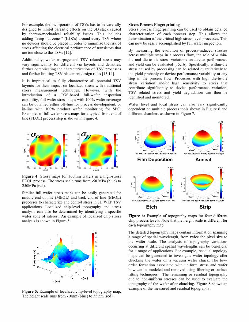
Wafer level and local stress can also vary significantly dependent on multiple process tools shown in Figure 6 and different chambers as shown in Figure 7.
Figure 6: Example of topography maps for four different chip process levels. Note that the height scale is different for each topography map.
The detailed topography maps contain information spanning a range of spatial wavelength, from twice the pixel size to the wafer scale. The analysis of topography variations occurring at different spatial wavelengths can be beneficial for a range of applications. For example, residual topology maps can be generated to investigate wafer topology after chucking the wafer on a vacuum wafer chuck. The low-order formation associated with uniform stress and wafer bow can be modeled and removed using filtering or surface fitting techniques. The remaining or residual topography due to non-uniform stresses can be used to evaluate the topography of the wafer after chucking. Figure 8 shows an example of the measured and residual topography.
σxx σyy
Film Deposition Anneal
Etch Strip
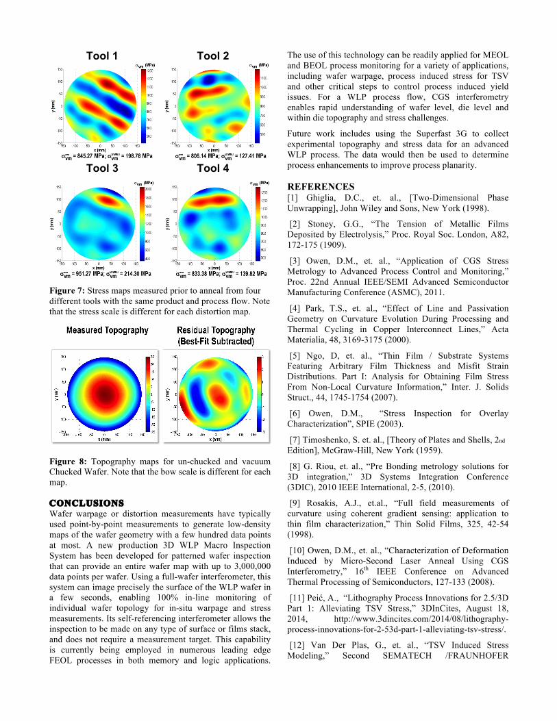
Tool 1 Tool 2
Tool 3 Tool 4
Figure 7: Stress maps measured prior to anneal from four different tools with the same product and process flow. Note that the stress scale is different for each distortion map.
Figure 8: Topography maps for un-chucked and vacuum Chucked Wafer. Note that the bow scale is different for each map. CONCLUSIONS Wafer warpage or distortion measurements have typically used point-by-point measurements to generate low-density maps of the wafer geometry with a few hundred data points at most. A new production 3D WLP Macro Inspection System has been developed for patterned wafer inspection that can provide an entire wafer map with up to 3,000,000 data points per wafer. Using a full-wafer interferometer, this system can image precisely the surface of the WLP wafer in a few seconds, enabling 100% in-line monitoring of individual wafer topology for in-situ warpage and stress measurements. Its self-referencing interferometer allows the inspection to be made on any type of surface or films stack, and does not require a measurement target. This capability is currently being employed in numerous leading edge FEOL processes in both memory and logic applications.
The use of this technology can be readily applied for MEOL and BEOL process monitoring for a variety of applications, including wafer warpage, process induced stress for TSV and other critical steps to control process induced yield issues. For a WLP process flow, CGS interferometry enables rapid understanding of wafer level, die level and within die topography and stress challenges.
Future work includes using the Superfast 3G to collect experimental topography and stress data for an advanced WLP process. The data would then be used to determine process enhancements to improve process planarity. REFERENCES [1] Ghiglia, D.C., et. al., [Two-Dimensional Phase Unwrapping], John Wiley and Sons, New York (1998).
[2] Stoney, G.G., “The Tension of Metallic Films Deposited by Electrolysis,” Proc. Royal Soc. London, A82, 172-175 (1909).
[3] Owen, D.M., et. al., “Application of CGS Stress Metrology to Advanced Process Control and Monitoring,” Proc. 22nd Annual IEEE/SEMI Advanced Semiconductor Manufacturing Conference (ASMC), 2011.
[4] Park, T.S., et. al., “Effect of Line and Passivation Geometry on Curvature Evolution During Processing and Thermal Cycling in Copper Interconnect Lines,” Acta Materialia, 48, 3169-3175 (2000).
[5] Ngo, D, et. al., “Thin Film / Substrate Systems Featuring Arbitrary Film Thickness and Misfit Strain Distributions. Part I: Analysis for Obtaining Film Stress From Non-Local Curvature Information,” Inter. J. Solids Struct., 44, 1745-1754 (2007).
[6] Owen, D.M., “Stress Inspection for Overlay Characterization”, SPIE (2003).
[7] Timoshenko, S. et. al., [Theory of Plates and Shells, 2nd
Edition], McGraw-Hill, New York (1959).
[8] G. Riou, et. al., “Pre Bonding metrology solutions for 3D integration,” 3D Systems Integration Conference (3DIC), 2010 IEEE International, 2-5, (2010).
[9] Rosakis, A.J., et.al., “Full field measurements of curvature using coherent gradient sensing: application to thin film characterization,” Thin Solid Films, 325, 42-54 (1998).
[10] Owen, D.M., et. al., “Characterization of Deformation Induced by Micro-Second Laser Anneal Using CGS Interferometry,” 16th IEEE Conference on Advanced Thermal Processing of Semiconductors, 127-133 (2008).
[11] Peić, A., “Lithography Process Innovations for 2.5/3D Part 1: Alleviating TSV Stress,” 3DInCites, August 18, 2014, http://www.3dincites.com/2014/08/lithography-process-innovations-for-2-53d-part-1-alleviating-tsv-stress/.
[12] Van Der Plas, G., et. al., “TSV Induced Stress Modeling,” Second SEMATECH /FRAUNHOFER

Workshop on Stress Management for 3D ICs using Through Silicon Vias, (2010).
[13] Le Texier, F.J. et. al., “Effect of TSV density on local stress concentration: Micro-Raman spectroscopy measurement and Finite Element Analysis,” Microelectronic Engineering, Volume 106, 139–143, (June 2013).
[14] Jiang, T. et. al., “Measurement and analysis of thermal stresses in 3D integrated structures containing through-silicon-vias,” Microelectronics Reliability 53, 53–62, (2013).
[15] Owen, D.M., et. al., “Correlation of Device Performance to Die-Level Stress Variations,” in Proc. Inter. Workshop Junction Tech., pp. 15-18, 2009.
[16] Owen, D.M., et. al., “The Effect of Die-Level Stress Variations on Device Performance,” in 17th IEEE Inter. Conf. on Adv. Thermal Processing of Semiconductors – RTP2009, 127-133, 2009.