characterization of pcb insertion loss with a new ... · characterization of pcb insertion loss...
TRANSCRIPT
Keysight Technologies Characterization of PCB Insertion Loss with a New Calibration Method
Application Note
Abstract
There are several existing techniques like Direct Loss Subtraction,
THRU-Relection-Line (TRL) calibration and Automatic Fixture Removal (AFR) with 2X THRU ixtures for characterizing PCB unit length insertion loss. In this application note, two methods will be discussed. 1) A new method for characterizing PCB loss by using AFR with 1X Open ixtures is proposed. This new method has been proven to have similar accuracy with TRL and AFR with 2X THRUs, but can save much more PCB area and measurement time; 2) based on measurements and simulations of transmission lines with different reference impedance, the measurement bandwidth, accuracy, eficiency and cost of these techniques are compared.
Introduction
It is critical to determine the PCB unit length loss characteristics for 1) material electrical parameters extraction; 2) PCB electrical performance estimation; 3) evaluation of the passive channel design; 4) PCB material selection; and 5) evaluation of the PCB fabrication quality, etc.
To characterize the insertion loss of the transmission lines on the PCB, test ixtures of coaxial to microstrip / stripline transitions (launches) are necessary to connect the PCB transmission line to the coaxial ports of the measurement instrument, such as a VNA or TDR. The test ixtures are not electri-cally transparent and their effects need to be removed from the total measurement.
There are several existing techniques like Direct Loss Subtraction, THRU-Relection-Line (TRL) as well as Automatic Fixture Removal (AFR) with 2X THRU ixtures that can be utilized to remove the effects of the test ixtures and characterize only the insertion loss of the PCB transmission lines. All of these methods have some assumptions and limitations in real application.
03 | Keysight | Characterization of PCB Insertion Loss with a New Calibration Method - Application Note
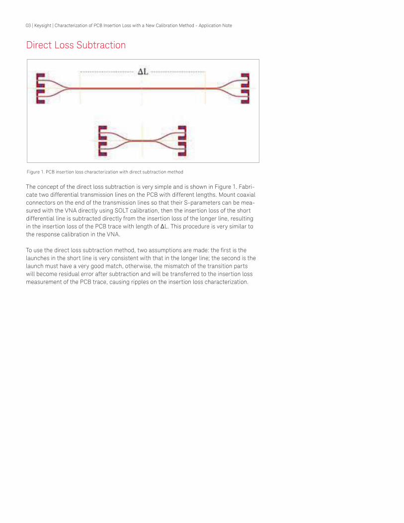
Direct Loss Subtraction
The concept of the direct loss subtraction is very simple and is shown in Figure 1. Fabri-cate two differential transmission lines on the PCB with different lengths. Mount coaxial connectors on the end of the transmission lines so that their S-parameters can be mea-
sured with the VNA directly using SOLT calibration, then the insertion loss of the short differential line is subtracted directly from the insertion loss of the longer line, resulting in the insertion loss of the PCB trace with length of ΔL. This procedure is very similar to the response calibration in the VNA.
To use the direct loss subtraction method, two assumptions are made: the irst is the launches in the short line is very consistent with that in the longer line; the second is the launch must have a very good match, otherwise, the mismatch of the transition parts will become residual error after subtraction and will be transferred to the insertion loss measurement of the PCB trace, causing ripples on the insertion loss characterization.
Figure 1. PCB insertion loss characterization with direct subtraction method
04 | Keysight | Characterization of PCB Insertion Loss with a New Calibration Method - Application Note
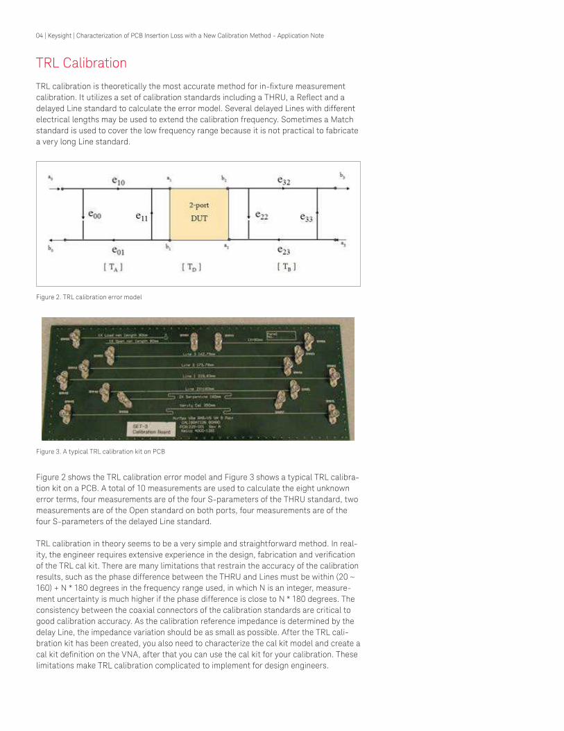
TRL Calibration
TRL calibration is theoretically the most accurate method for in-ixture measurement calibration. It utilizes a set of calibration standards including a THRU, a Relect and a delayed Line standard to calculate the error model. Several delayed Lines with different electrical lengths may be used to extend the calibration frequency. Sometimes a Match standard is used to cover the low frequency range because it is not practical to fabricate
a very long Line standard.
Figure 2 shows the TRL calibration error model and Figure 3 shows a typical TRL calibra-
tion kit on a PCB. A total of 10 measurements are used to calculate the eight unknown error terms, four measurements are of the four S-parameters of the THRU standard, two measurements are of the Open standard on both ports, four measurements are of the four S-parameters of the delayed Line standard.
TRL calibration in theory seems to be a very simple and straightforward method. In real-ity, the engineer requires extensive experience in the design, fabrication and veriication of the TRL cal kit. There are many limitations that restrain the accuracy of the calibration results, such as the phase difference between the THRU and Lines must be within (20 ~ 160) + N * 180 degrees in the frequency range used, in which N is an integer, measure-
ment uncertainty is much higher if the phase difference is close to N * 180 degrees. The consistency between the coaxial connectors of the calibration standards are critical to
good calibration accuracy. As the calibration reference impedance is determined by the delay Line, the impedance variation should be as small as possible. After the TRL cali-bration kit has been created, you also need to characterize the cal kit model and create a cal kit deinition on the VNA, after that you can use the cal kit for your calibration. These limitations make TRL calibration complicated to implement for design engineers.
Figure 2. TRL calibration error model
Figure 3. A typical TRL calibration kit on PCB

05 | Keysight | Characterization of PCB Insertion Loss with a New Calibration Method - Application Note
Automatic Fixture Removal (AFR) with 2X THRU
The test structures used in 2X THRU AFR[1][2] (shown in Figure 4) for characterizing the PCB insertion loss is very similar to those used in the Direct Subtraction method, but 2X THRU is based on ixture model de-embedding[4] and is more accurate than the Direct Subtraction method. In 2X THRU AFR, the short line (or so called 2X THRU) can be math-
ematically separated to two parts – ixture A and ixture B based on time domain gating[3] and signal low diagram calculations, then the extracted S-parameters of ixture A and ixture B can be de-embedded from the longer line measurement (so called DUT). The de-embedding result is the four S-parameters of the PCB trace with length of ΔL.
The 2X THRU AFR also has some limitations. First, the launches of the shorter line must be consistent with that in the longer line, left to left, right to right respectively. Any
inconsistency between the two will cause an error in the de-embedding model and error in the PCB insertion loss measurement. Second, the return loss and insertion loss of the 2X THRU must not cross each other in the frequency range concerned, often a 5 dB separation is required to make sure the ixture has wider bandwidth than the DUT. Other-wise, the de-embedding result may show some gain, which is not correct.
The 2X THRU AFR has been accepted by commercial companies like Huawei to replace TRL calibration in the PCB loss characterization process because it has been validated to
have the similar accuracy with TRL calibration, but is much simpler.
Figure 4. PCB loss characterization with 2X THRU AFR

06 | Keysight | Characterization of PCB Insertion Loss with a New Calibration Method - Application Note
Characterization of PCB Insertion Loss with New 1X AFR
With the new method of 1X AFR using an Open standard which was introduced in early 2014, we can characterize the PCB loss with two Open ixtures of different lengths, shown in Figure 5. With this method, we can save half PCB areas than 2X THRU AFR. As the differential Open ixture requires a 2-port measurement rather than 4-port measure-
ment of the 2X THRU, with 1X AFR we can save more calibration and measurement time.
The procedure of using 1X AFR in characterizing the PCB insertion loss is as follows:
1. Extract 4-port S-parameters of the Open ixtures from 2-port measurements
With 1X AFR, the 4-port S-parameters of the two Open ixtures can be extracted from the 2-port Open measurements respectively. The characterization is also based on time domain gating and signal low diagram, similar to the 2X THRU AFR.
Notice: The ixture extraction procedure above has been integrated in Keysight PLTS software and PNA irmware.
2. After the 4-port S-parameters of the two Open ixtures have all been acquired, the 4-port data of the short Open ixture can be de-embedded from the 4-port data of the long Open ixture, resulting in the 4-port S-parameters of PCB with length of ΔL, from which the differential insertion loss can be determined.
The 1X AFR also has some limitations. First, similar to 2X THRU AFR, the launches of the two Opens must be consistent. Any inconsistency between the two will cause error in the de-embedding model and error in the PCB insertion loss measurement. Second, the impedance variations of the PCB traces must be as small as possible, especially when getting close to the Open end. As bandpass time domain gating is used to extract the ixture insertion loss from the Open measurement in 1X AFR, the mismatch close to the Open response may still be included after gating and may cause ripples on the extracted insertion loss. This effect will be discussed in more detail.
Figure 5. Two Open ixtures used for extracting PCB insertion loss with length of ΔL

07 | Keysight | Characterization of PCB Insertion Loss with a New Calibration Method - Application Note
Comparisons of Different Methods in Characterizing PCB Insertion Loss with Simulations
To validate the performance of the new 1X AFR and compare the results of all the above methods, ADS simulations were used to create the test structures of the PCB trace without launch, the two 2X THRUs and the two Open ixtures with different lengths. S-parameter simulations can be done to acquire all the S-parameters of these structures. After that, Direct Loss Subtraction, 2X THRU AFR and 1X AFR are used to characterize the insertion loss of the PCB trace and compared to the actual data. The lengths of all the structures are shown in the table below.
Dielectric Constant: 3.85
Reference impedance of 100 ohm and 90 ohm are validated respectively. Two cascaded short transmission lines with impedance of 104 ohm and 92 ohm are used to emulate the impedance variations on coaxial connectors.
The S-parameters of the longer Open standard can be simulated with the schematic shown in Figure 6. Similarly, the schematic can be modiied to simulate the S-parameters of the shorter Open, the long 2X THRU and the short 2X THRU.
Line length (mil)
PCB trace length without launches 11000
Launch 150
2X THRU AFR Longer line (Direct Subtraction longer line) 11300
2X THRU AFR Shorter line (Direct Subtraction shorter line) 1300
1X AFR Longer Open 11150
1X AFR Shorter Open 1150
Figure 6. Schematic for simulating the s2p of the longer Open ixture
08 | Keysight | Characterization of PCB Insertion Loss with a New Calibration Method - Application Note
Comparisons of Different Methods in Characterizing PCB Insertion Loss with Simulations continued
In the comparisons below, the actual data of the PCB trace is taken as the reference, the results of Direct Loss Subtraction, 2X THRU AFR and 1X AFR are compared to the actual data independently and the differences are calculated, the maximum error compared to actual data can be used as the index of the performance of that method.
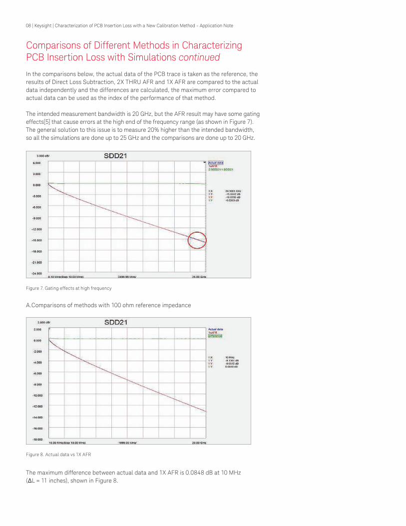
The intended measurement bandwidth is 20 GHz, but the AFR result may have some gating effects[5] that cause errors at the high end of the frequency range (as shown in Figure 7). The general solution to this issue is to measure 20% higher than the intended bandwidth, so all the simulations are done up to 25 GHz and the comparisons are done up to 20 GHz.
A.Comparisons of methods with 100 ohm reference impedance
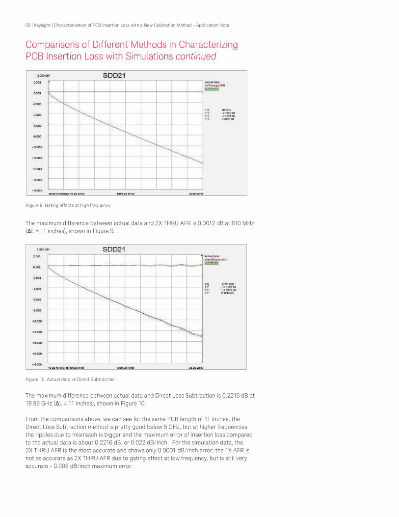
The maximum difference between actual data and 1X AFR is 0.0848 dB at 10 MHz (ΔL = 11 inches), shown in Figure 8.
Figure 7. Gating effects at high frequency
Figure 8. Actual data vs 1X AFR
09 | Keysight | Characterization of PCB Insertion Loss with a New Calibration Method - Application Note
Figure 9. Gating effects at high frequency
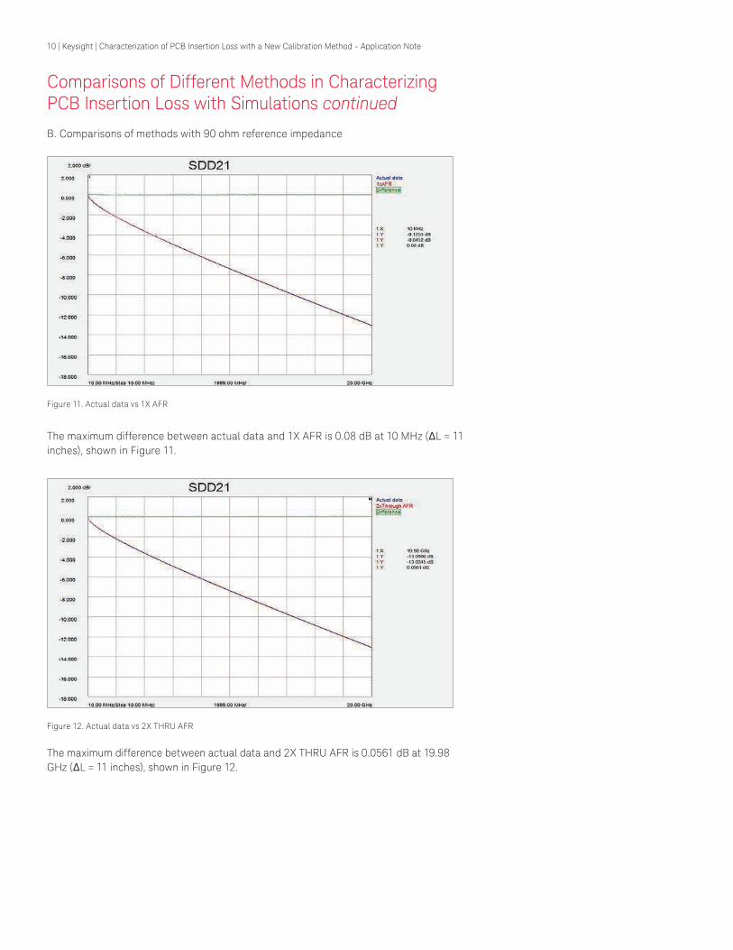
The maximum difference between actual data and 2X THRU AFR is 0.0012 dB at 810 MHz (ΔL = 11 inches), shown in Figure 9.
The maximum difference between actual data and Direct Loss Subtraction is 0.2216 dB at 19.99 GHz (ΔL = 11 inches), shown in Figure 10.
From the comparisons above, we can see for the same PCB length of 11 inches, the Direct Loss Subtraction method is pretty good below 5 GHz, but at higher frequencies the ripples due to mismatch is bigger and the maximum error of insertion loss compared to the actual data is about 0.2216 dB, or 0.022 dB/inch. For the simulation data, the 2X THRU AFR is the most accurate and shows only 0.0001 dB/inch error; the 1X AFR is not as accurate as 2X THRU AFR due to gating effect at low frequency, but is still very accurate - 0.008 dB/inch maximum error.
Figure 10. Actual data vs Direct Subtraction
Comparisons of Different Methods in Characterizing PCB Insertion Loss with Simulations continued
10 | Keysight | Characterization of PCB Insertion Loss with a New Calibration Method - Application Note
Comparisons of Different Methods in Characterizing PCB Insertion Loss with Simulations continued
B. Comparisons of methods with 90 ohm reference impedance
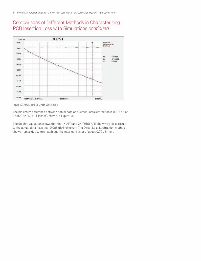
The maximum difference between actual data and 1X AFR is 0.08 dB at 10 MHz (ΔL = 11 inches), shown in Figure 11.
The maximum difference between actual data and 2X THRU AFR is 0.0561 dB at 19.98 GHz (ΔL = 11 inches), shown in Figure 12.
Figure 11. Actual data vs 1X AFR
Figure 12. Actual data vs 2X THRU AFR
11 | Keysight | Characterization of PCB Insertion Loss with a New Calibration Method - Application Note
Comparisons of Different Methods in Characterizing PCB Insertion Loss with Simulations continued
The maximum difference between actual data and Direct Loss Subtraction is 0.193 dB at 17.55 GHz (ΔL = 11 inches), shown in Figure 13.
The 90 ohm validation shows that the 1X AFR and 2X THRU AFR show very close result to the actual data (less than 0.005 dB/inch error). The Direct Loss Subtraction method shows ripples due to mismatch and the maximum error of about 0.02 dB/inch.
Figure 13. Actual data vs Direct Subtraction
12 | Keysight | Characterization of PCB Insertion Loss with a New Calibration Method - Application Note
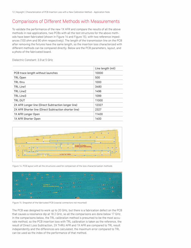
Comparisons of Different Methods with Measurements
To validate the performance of the new 1X AFR and compare the results of all the above methods in real applications, two PCBs with all the test structures for the above meth-
ods have been fabricated (shown in Figure 14 and Figure 15), with two reference imped-
ances (100 ohm and 90 ohm respectively). The length of the transmission line on the PCB after removing the ixtures have the same length, so the insertion loss characterized with different methods can be compared directly. Below are the PCB parameters, layout, and a photo of the fabricated board.
Dielectric Constant: 3.9 at 5 GHz
The PCB was designed to work up to 20 GHz, but there is a fabrication defect on the PCB that causes a resonance dip at 18.2 GHz, so all the comparisons are done below 17 GHz. In the comparisons below, the TRL calibration method is presumed to be the most accu-
rate method, so the PCB insertion loss with TRL calibration is taken as the reference, the result of Direct Loss Subtraction, 2X THRU AFR and 1X AFR are compared to TRL result independently and the differences are calculated, the maximum error compared to TRL can be used as the index of the performance of that method.
Line length (mil)
PCB trace length without launches 10000
TRL Open 500
TRL thru 1000
TRL Line1 3480
TRL Line2 1496
TRL Line3 1099
TRL DUT 11000
2X AFR Longer line (Direct Subtraction longer line) 12327
2X AFR Shorter line (Direct Subtraction shorter line) 2327
1X AFR Longer Open 11400
1X AFR Shorter Open 1400
Figure 14. PCB layout with all the structures used for comparison of the loss characterization methods
Figure 15. Snapshot of the fabricated PCB (coaxial connectors not mounted)

13 | Keysight | Characterization of PCB Insertion Loss with a New Calibration Method - Application Note
Comparisons of Methods on PCB with 100 Ohm Reference Impedance
The maximum difference between TRL calibration and 1X AFR is 0.1831 dB at 14.82 GHz (ΔL = 10 inches), shown in Figure 16.
The maximum difference between TRL calibration and 2X THRU AFR is 0.2118 dB at 14.66 GHz (ΔL = 10 inches), shown in Figure 17.
Figure 16. TRL calibration vs 1X AFR
Figure 17. TRL calibration vs 2X THRU AFR
14 | Keysight | Characterization of PCB Insertion Loss with a New Calibration Method - Application Note
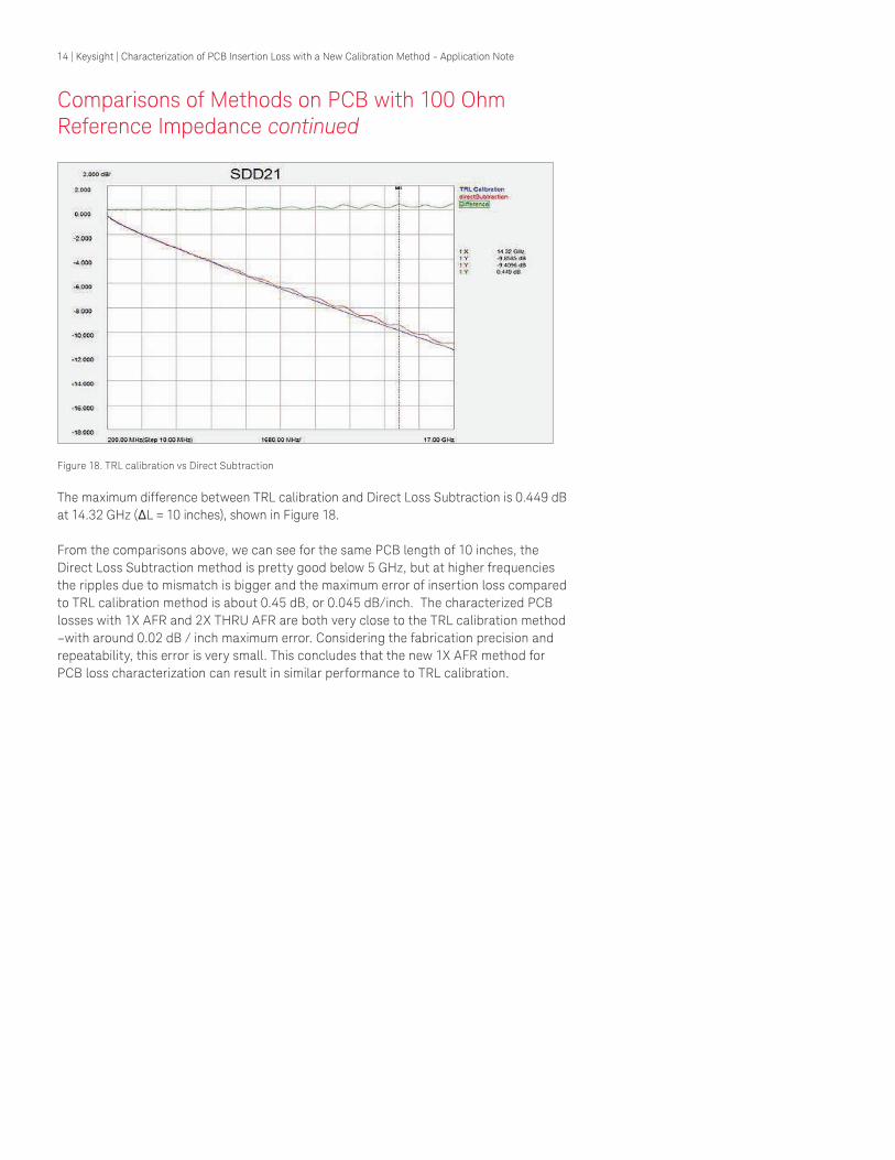
Comparisons of Methods on PCB with 100 Ohm Reference Impedance continued
The maximum difference between TRL calibration and Direct Loss Subtraction is 0.449 dB at 14.32 GHz (ΔL = 10 inches), shown in Figure 18.
From the comparisons above, we can see for the same PCB length of 10 inches, the Direct Loss Subtraction method is pretty good below 5 GHz, but at higher frequencies the ripples due to mismatch is bigger and the maximum error of insertion loss compared to TRL calibration method is about 0.45 dB, or 0.045 dB/inch. The characterized PCB losses with 1X AFR and 2X THRU AFR are both very close to the TRL calibration method –with around 0.02 dB / inch maximum error. Considering the fabrication precision and repeatability, this error is very small. This concludes that the new 1X AFR method for PCB loss characterization can result in similar performance to TRL calibration.
Figure 18. TRL calibration vs Direct Subtraction
15 | Keysight | Characterization of PCB Insertion Loss with a New Calibration Method - Application Note
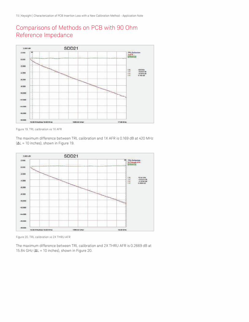
Comparisons of Methods on PCB with 90 Ohm Reference Impedance
The maximum difference between TRL calibration and 1X AFR is 0.169 dB at 420 MHz (ΔL = 10 inches), shown in Figure 19.
The maximum difference between TRL calibration and 2X THRU AFR is 0.2669 dB at 15.84 GHz (ΔL = 10 inches), shown in Figure 20.
Figure 19. TRL calibration vs 1X AFR
Figure 20. TRL calibration vs 2X THRU AFR
16 | Keysight | Characterization of PCB Insertion Loss with a New Calibration Method - Application Note
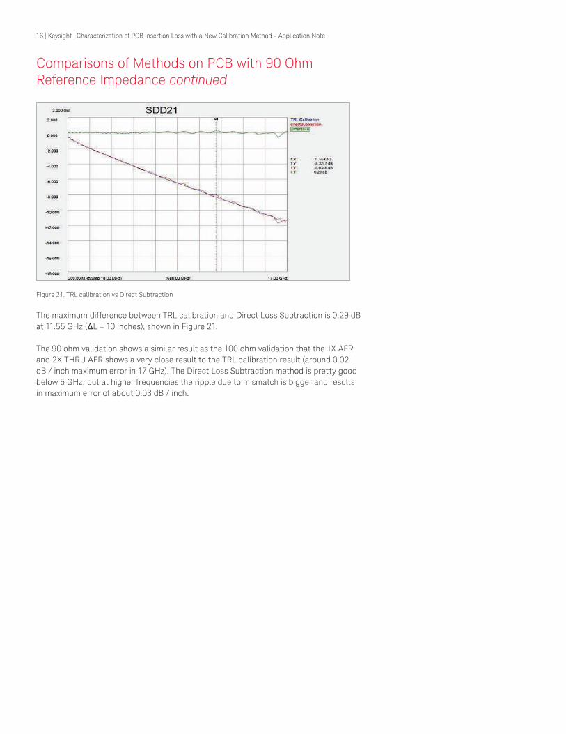
Comparisons of Methods on PCB with 90 Ohm Reference Impedance continued
The maximum difference between TRL calibration and Direct Loss Subtraction is 0.29 dB at 11.55 GHz (ΔL = 10 inches), shown in Figure 21.
The 90 ohm validation shows a similar result as the 100 ohm validation that the 1X AFR and 2X THRU AFR shows a very close result to the TRL calibration result (around 0.02 dB / inch maximum error in 17 GHz). The Direct Loss Subtraction method is pretty good below 5 GHz, but at higher frequencies the ripple due to mismatch is bigger and results in maximum error of about 0.03 dB / inch.
Figure 21. TRL calibration vs Direct Subtraction

17 | Keysight | Characterization of PCB Insertion Loss with a New Calibration Method - Application Note
Considerations on the Gating Range of 1X AFR Method
In the 1X AFR method, bandpass time domain gating is used for the extraction of the ix-
ture insertion loss from the Open standard. The gating range has impacts on the accuracy of the extracted ixture insertion loss and the optimum gating range is the compromise of two aspects: if the gating range is too narrow to the Open response, part of the Open response may be gated off and causes the extracted insertion loss to have some ripples; if the gating range is too wide, although the complete Open response will be maintained, some mismatch effects caused by the impedance variations of the PCB trace will also be included after gating and introduce some ripples to the extracted insertion loss.
Figure 22 shows the gating range of 4x system rise time using the longer Open standard of 100 ohm.
Figure 23 shows the gating range of 20x system rise time using the same Open standard.
Figure 22. TDD11 Time domain impulse response of the differential Open standard. If the gating range is too narrow, part of the Open response will be gated off.
Figure 23. TDD11 Time domain impulse response of the differential Open standard. If the gating range is too wide, some mismatch will be included in the extracted insertion loss.
18 | Keysight | Characterization of PCB Insertion Loss with a New Calibration Method - Application Note
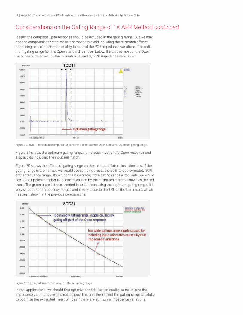
Ideally, the complete Open response should be included in the gating range. But we may need to compromise that to make it narrower to avoid including the mismatch effects, depending on the fabrication quality to control the PCB impedance variations. The opti-mum gating range for this Open standard is shown below. It includes most of the Open response but also avoids the mismatch caused by PCB impedance variations.
Figure 24 shows the optimum gating range. It includes most of the Open response and also avoids including the input mismatch.
Figure 25 shows the effects of gating range on the extracted ixture insertion loss. If the gating range is too narrow, we would see some ripples at the 20% to approximately 30% of the frequency range, shown on the blue trace; if the gating range is too wide, we would see some ripples at higher frequencies caused by the mismatch effects, shown as the red trace. The green trace is the extracted insertion loss using the optimum gating range, it is very smooth at all frequency ranges and is very close to the TRL calibration result, which has been shown in the previous comparisons.
In real applications, we should irst optimize the fabrication quality to make sure the impedance variations are as small as possible, and then select the gating range carefully to optimize the extracted insertion loss if there are still some impedance variations.
Figure 24. TDD11 Time domain impulse response of the differential Open standard. Optimum gating range.
Figure 25. Extracted insertion loss with different gating range
Considerations on the Gating Range of 1X AFR Method continued

19 | Keysight | Characterization of PCB Insertion Loss with a New Calibration Method - Application Note
Conclusion
In this application note, we proposed using the new 1X AFR technique to characterize the PCB insertion loss. ADS simulations and real measurements on fabricated PCB structures have been done for the comparisons of extracted PCB insertion loss with different meth-
ods[6]. The new 1X AFR method is proven to have similar performance with the traditional TRL calibration and 2X THRU AFR methods, but it can save more PCB area, calibration and measurement time. When using 1X AFR method in this process, the Open standard should be optimized to have small impedance variations on the PCB trace, care needs to be taken in selecting the optimum gating range to achieve the best result.
The performance comparisons of all these methods are summarized in the table below:
References
[1] Vahé Adamian, Brad Cole and Jim Nadolny, “A Novel Procedure for Characterization of Multi-port High Speed Balanced Devices”, IEC DesignCon 2007.
[2] Joel Dunsmore, Cheng Ning and Zhang Yongxun, “Characterizations of asymmetric ixtures with a two-gate approach”, ARFTG 2011.
[3] Archambeault, B., Connor, S. and Diepenbrock, J.C., “Time domain gating of frequency domain S-parameter data to remove connector end effects for PCB and cable applications,” 2006 IEEE International Symposium on EMC, Volume 1, August 14-18, 2006, pp 199-202.
[4] De-embedding and Embedding S-Parameter Networks Using a Vector Network Analyzer, Agilent Application Note 1364-1, June 2004.
[5] Joel Dunsmore, “Handbook of Microwave Component Measurements with Advanced VNA Techniques”, page 231, Wiley.
[6] Mike Resso and Eric Bogatin, “Signal Integrity Characterization Techniques”, published book, International Engineering Consortium, 2009, irst edition.
Direct Loss
Subtraction TRL calibration 2x THRU AFR 1X AFR
Complexity Easy Complicated Easy Easy
Accuracy Low High High High
Cost Low High Low Lowest
Measurement
Bandwidth Low High High High

myKeysight
www.keysight.com/find/mykeysight
A personalized view into the information most relevant to you.
Three-Year Warranty
www.keysight.com/find/ThreeYearWarranty
Keysight’s commitment to superior product quality and lower total cost of ownership. The only test and measurement company with three-year warranty standard on all instruments, worldwide.
Keysight Assurance Plans
www.keysight.com/find/AssurancePlans
Up to five years of protection and no budgetary surprises to ensure your
instruments are operating to specification so you can rely on accurate measurements.
www.keysight.com/go/quality
Keysight Technologies, Inc.
DEKRA Certified ISO 9001:2008 Quality Management System
Keysight Channel Partners
www.keysight.com/find/channelpartners
Get the best of both worlds: Keysight’s measurement expertise and product breadth, combined with channel partner convenience.
www.keysight.com/find/plts
For more information on Keysight Technologies’ products, applications or
services, please contact your local Keysight
office. The complete list is available at:www.keysight.com/find/contactus
Americas Canada (877) 894 4414Brazil 55 11 3351 7010Mexico 001 800 254 2440United States (800) 829 4444
Asia PaciicAustralia 1 800 629 485China 800 810 0189Hong Kong 800 938 693India 0124 229 2010Japan 0120 (421) 345Korea 080 769 0800Malaysia 1 800 888 848Singapore 1 800 375 8100Taiwan 0800 047 866Other AP Countries (65) 6375 8100
Europe & Middle East
Austria 0800 001122Belgium 0800 58580Finland 0800 523252France 0805 980333Germany 0800 6270999Ireland 1800 832700Israel 1 809 343051Italy 800 599100Luxembourg +32 800 58580Netherlands 0800 0233200Russia 8800 5009286Spain 800 000154Sweden 0200 882255Switzerland 0800 805353
Opt. 1 (DE)Opt. 2 (FR)Opt. 3 (IT)
United Kingdom 0800 0260637
For other unlisted countries:www.keysight.com/find/contactus(BP-02-06-15)
20 | Keysight | Characterization of PCB Insertion Loss with a New Calibration Method - Application Note
This information is subject to change without notice.© Keysight Technologies, 2015Published in USA, March 26, 20155992-0656ENwww.keysight.com