characterisation of a commercial active screen plasma nitriding
TRANSCRIPT

i
Characterisation of a Commercial Active Screen Plasma Nitriding
System
by
Paul Hubbard
A thesis submitted for the degree of Doctor of Philosophy
at the Department of Applied Physics.
RMIT University. Australia.
(October 2007)

ii
Declaration of Originality I certify that except where due acknowledgement has been made, the work is that of
the author alone; the work has not been submitted previously, in whole or in part, to
qualify for any other academic award; the content of the thesis is the result of work
which has been carried out since the official commencement date of the approved
research program; and, any editorial work, paid or unpaid, carried out by a third party
is acknowledged.
Paul Hubbard
06/03/2008

iii
Acknowledgements Instrumental to the success of this study has been the input of my three supervisors:
Prof. Dougal McCulloch, Prof. Derry Doyle and Dr. Steve Dowey. I would like to offer
you guys a sincere thank you for answering the many phone calls of mine, pointing
me in the right direction and remaining positive about the results however they
seemed. Also, the input outside of working hours, time spent on the weekends and
at odd hours through the night all added to the content presented in this thesis.
I would also like to thank the Directors and Chief Executive Officer of Sutton Tools
Pty Ltd for kindly allowing access to their nitriding facility. Clearly without access to
the commercial equipment, this project would have been severely hampered and
would never have achieved the current outcomes.
In addition, I would also like to thank the staff of the physics department, particularly
Phil Francis and Geoffrey Carter. I enjoyed the conversations we had about various
things and especially liked working together when it came to issues relating to the
physics department. Some of these included the drinking water problem, and the
theft of my laptop (and others) mid way through my project.
Throughout this study, there were people involved with helping me to use analysis
equipment. These people included, Hans Brinkies, Dr. John Long, Dr. Ken Short, Dr.
Kay Latham, A Prof. Salvy Russo, A Prof. Johan Du Plessis, David Stavely and Ju
Lin Peng. So to all of the aforementioned, I would like to say thank you for your
patience and support and of course answering my many phone calls and replying to
my many emails.
And to all of the people behind the scenes, the following is for you.
Martin Meli, my mate that I have known for many years, always around the corner, “I
will be there in five minutes” and “have you got milk?” or “hey, I am glad you’re here, I
need a hand”. Also, “If you pay peanuts, you get monkeys” and “I got no money” or “I
am busy, I got to go”. Thanks mate, you know what I mean.

iv
Christian Maunders, I hope you are coming back soon. There are plenty of swap
meets and car shows we need to go to. I particularly remember the character
building trip where we used my maglite torch as headlights all the way back from
Portland and the time we broke down in your boat off the coast, lucky we got
rescued!
Gorgi Kostovski and William Wheatley, thanks for helping me to buy my house and
supporting me through my double degree. If only we knew what we were getting
ourselves in for. Thanks guys.
Adrian Trinchi, you were always not too far away when I needed to have a chat.
Your family, particularly your mum and the pasta she cooked and would not let me
leave until I ate. Thanks very much mate.
The security boys: Michael Canik, Frank Cesko, Yucel Tellipinar. To the long nights
we had together. I truly enjoyed the many hours we spent together and chatted.
Thanks for watching my back, and saving my neck.
William Agius, well, “It’s hard to soar with the eagles when you are flying with the
magpies”. Thanks Bill, you always reminded me your day was much worse than
mine.
And to the other people that had an input along the way, Matthew Taylor, Akin Budi
and James Partridge, thanks guys.
Todor and Zorica, thank you very much for all of the dinners you allowed me to have
at your house. Thank you for making me feel welcome at your house and for your
belief in me and my capabilities when it came to my work. I especially appreciate the
positive outlook you guys had and gave me with respect to the jobs I had to do on the
many weekends throughout my PhD.
Igor and Zana, thanks guys for the time we all spent together, the many lengthy
discussions and dinners we had. This time was thoroughly enjoyed and I am looking
forward to more good times.

v
To my partner, Nevena, thank you for teaching me that those things that seem really
bad are usually not that bad at all. You were always there by my side to offer me
your ear for my problems and ready to offer me your opinion for which I value greatly.
Also, thank you very much for being patient with me while I did the things that I had
to do.
Most importantly to my family: Dad, Mum, Daniella, Andrew, Rosetta, Jac, Darcie,
and Harrison. Without you I definitely would not have written this. You were always
there even when I could not see through the woods, keeping things in perspective for
me and always staying positive. Thank you is not enough thanks for all that you guys
did for me and for all the support. The support came in many different ways and I will
never forget what you have all done. Now it is my turn!

vi
Authors Publications 1: Influence of bias and in situ cleaning on through cage (TC) or active
screen plasma nitrided steels.
Surface Engineering 22 (4): 243-247 AUG 2006.
P. Hubbard, S. J. Dowey, E.D. Doyle and D. G. McCulloch.

vii
Conference Presentations
1: The 1st International Conference on Heat Treatment and Surface Engineering
of Tools and Dies, 2005 – Pula, Croatia.
Speaker: The influence of Bias and In-Situ Cleaning on Through Cage
(TC) or Active Screen Plasma Nitrided (ASPN) Steels, P. Hubbard, S. J.
Dowey, E.D. Doyle and D. G. McCulloch.
2: The 2nd International Conference on Heat Treatment and Surface Engineering
in Automotive Applications, 2005 – Riva del Garda, Italy.
Speaker: A study of key processing parameters in the Active Screen
Plasma Nitriding (ASPN) of steels, E. D. Doyle, P. Hubbard, D. G.
McCulloch, S. J. Dowey.
3: The 15th International Federation for Heat Treatment and Surface Engineering
and Surface Modification Technologies, 2006 – Vienna, Austria.
Speaker: A Basic Contribution to a Study of the Active Screen Plasma
Nitriding Process, P. Hubbard, D. G. McCulloch, E. D. Doyle and S. J.
Dowey, J. N. Georges.
4: The 9th Biennial Symposium of the Australian Microbeam Analysis Society,
2007 – Melbourne, Australia.
Speaker: Analysis of active screen plasma nitrided samples under
various process conditions – to bias, or not to bias: that is the question,
P. Hubbard, D. G. McCulloch, E. D. Doyle and S. J. Dowey.

viii
Abstract Nitriding is a plasma based processing technique that is used to improve the surface
properties of components and products in many areas including the aerospace,
automotive and biomedical industries to name a few. Active Screen Plasma Nitriding
(ASPN) is a relatively new nitriding technique which has potential advantages over
the more traditional nitriding techniques such as Direct Current (DC) plasma nitriding
where high substrate biases can be problematic. However, there is considerable
debate as to the mechanism for nitriding in ASPN. This thesis focuses on
investigating the mechanism for nitriding in a commercial ASPN system.
Commercial ASPN treatments of nitrideable alloy steels were found to be
unsatisfactory unless a sufficient bias was applied. The level of bias required to
produce a satisfactory nitriding response, in terms of the cross sectional hardness,
was found to depend on the concentration of strong alloy nitride forming elements
present in the steel.
Although active screen material was found to be transferred to the workload, no
evidence was found that this process played a significant role in enhancing the
nitriding response. The primary mechanism for nitrogen mass transfer in ASPN was
found to be dependent on the active screen/workload separation distance. When this
separation is small (less than approximately 10cm for the conditions used in this
study) then nitrogen mass transfer in the form of energetic ions or neutrals can occur
between the active screen and the workload. This allows samples to be treated
without a substrate bias. On the other hand, when the active screen/workload
separation distance is large (greater than approximately 10cm) as is normally the
case in a commercial environment, this mechanism for nitrogen mass transfer breaks
down and a substrate bias is essential. In this latter case, nitrogen ions attracted to
the workload using a bias is the primary nitrogen mass transfer mechanism and the
role of the active screen is primarily to uniformly heat the workload.

ix
Table of Contents 1 Introduction .................................................................. 1
1.1 Why the need to harden materials ................................................................2
1.2 Aims and Objectives .....................................................................................3
1.3 Thesis Organisation and Scope ....................................................................3
2 Background .................................................................. 5
2.1 What is a hard material? ...............................................................................6
2.2 A brief introduction to the metallurgy of Nitriding...........................................7
2.2.1 The Fe-N phase diagram .......................................................................7
2.2.2 The Nitriding process ...........................................................................10
2.2.2.1 The compound layer.........................................................................11
2.2.2.2 The Diffusion Zone ...........................................................................12
2.3 Historical Review of Nitriding ......................................................................12
2.4 Gas Nitriding ...............................................................................................13
2.5 Salt Bath Nitriding / Liquid Nitriding.............................................................15
2.6 Direct Current Plasma Nitriding...................................................................16
2.7 Post Discharge Nitriding..............................................................................23
2.8 Active Screen Plasma Nitriding...................................................................25
2.9 Summary.....................................................................................................30
3 Experimental Techniques.......................................... 31
3.1 The materials investigated ..........................................................................31
3.2 Plasma Etch................................................................................................33
3.3 Active Screen Plasma Nitriding (ASPN) system and conditions .................33
3.4 The bias power supply ................................................................................35
3.5 Temperature control and the Active Screen Power supply .........................37
3.6 Hardness Response....................................................................................37
3.6.1 Surface Hardness Measurements........................................................38
3.6.2 Cross Sectional preparation and Hardness Measurements.................39
3.7 Glow-Discharge Optical Emission Spectroscopy ........................................40
3.8 Electron Microscopy....................................................................................41
3.8.1 Scanning Electron Microscopy.............................................................41
3.8.2 Transmission Electron Microscopy ......................................................42
3.8.2.1 Cross Sectional TEM........................................................................43
3.8.2.2 Energy Filtered TEM ........................................................................44
3.9 X-Ray Diffraction.........................................................................................44
4 Characterisation of the commercial ASPN system. 45
4.1 Overview of ASPN system operation ..........................................................45
4.2 The effect of bias and etching on the nitriding response.............................46
4.2.1 Results and Discussion........................................................................48
4.2.1.1 Surface Hardness.............................................................................48
4.2.1.2 Cross Sectional Hardness Profiles ...................................................50
4.2.1.3 Glow-Discharge Optical Emission Spectroscopy..............................53
4.2.2 Summary .............................................................................................55
4.3 Effect of bias on the nitriding response .......................................................56
4.3.1 Results and Discussion........................................................................57
4.3.1.1 Surface Hardness.............................................................................57
4.3.1.2 Cross Sectional Hardness Profiles ...................................................58
4.3.1.3 Glow-Discharge Optical Emission Spectroscopy..............................60

x
4.3.2 Summary .............................................................................................61
4.4 Effect of gas mixture on nitriding response .................................................62
4.4.1 Experiment...........................................................................................62
4.4.2 Results and Discussion........................................................................63
4.4.2.1 Effect of gas mixture on the bias voltage..........................................63
4.4.2.2 Surface Hardness.............................................................................64
4.4.2.3 Cross Sectional Hardness Profiles ...................................................65
4.4.2.4 Glow-Discharge Optical Emission Spectroscopy..............................66
4.4.2.5 Microstructure...................................................................................67
4.4.2.6 Compound layer tests ......................................................................70
4.4.2.7 X-Ray Diffraction ..............................................................................71
4.4.2.8 Model for the compound layer thickness and case depth.................73
4.4.3 Summary .............................................................................................75
4.5 Conclusion ..................................................................................................76
5 The role of the Active Screen in ASPN..................... 77
5.1 The effect of active screen material on the nitriding response ....................77
5.1.1 Experiment...........................................................................................77
5.1.2 Results and Discussion........................................................................78
5.1.2.1 Surface Hardness.............................................................................79
5.1.2.2 Cross Sectional Hardness Profiles ...................................................81
5.1.2.3 Glow-Discharge Optical Emission Spectroscopy..............................84
5.1.3 Summary .............................................................................................86
5.1.4 Mass transfer from the Active Screen ..................................................87
5.1.5 The nature of material transferred........................................................88
5.1.5.1 Experimental ....................................................................................88
5.1.6 Results and Discussion........................................................................89
5.1.6.1 Active Screen Material Deposition: MS Screen ................................89
5.1.6.2 Active Screen Material Deposition: HA Screen ................................95
5.1.7 The effect of mass transfer on the nitriding response ..........................98
5.1.8 Isolating the Active Screen ................................................................102
5.1.9 Summary ...........................................................................................105
5.2 Conclusion ................................................................................................105
6 Further ASPN Investigations................................... 107
6.1 The nitriding response as a function of height in the chamber ..................107
6.1.1 Results and Discussion......................................................................109
6.1.1.1 Surface Hardness...........................................................................109
6.1.1.2 Cross Sectional Hardness Profiles .................................................110
6.1.1.3 Glow-Discharge Optical Emission Spectroscopy............................111
6.1.2 Summary ...........................................................................................113
6.2 Proximity Experiments ..............................................................................113
6.2.1 Experimental set up ...........................................................................113
6.2.2 Results and Discussion......................................................................115
6.2.2.1 Surface Hardness...........................................................................115
6.2.2.2 Cross Sectional Hardness Profiles .................................................115
6.2.2.3 Glow-Discharge Optical Emission Spectroscopy............................117
6.2.3 Summary ...........................................................................................119
6.3 Separation of the mini screen and the samples ........................................119
6.3.1 Experimental set up ...........................................................................119
6.3.2 Results and Discussion......................................................................120
6.3.2.1 Surface Hardness...........................................................................120
6.3.2.2 Cross Sectional Hardness Profiles .................................................121

xi
6.3.2.3 Glow-Discharge Optical Emission Spectroscopy............................123
6.4 Discussion on the role of Biased Grids in ASPN.......................................125
6.4.1 Biased Grids in Plasma Immersion Ion Implantation..........................125
6.4.2 Mechanisms for nitrogen mass transfer using a mini active screen...127
6.4.3 The effect of the active screen to sample separation.........................129
6.4.4 Summary ...........................................................................................132
6.4.5 Conclusion .........................................................................................133
7 Conclusions and future work.................................. 134
7.1 The role of the active screen in ASPN ......................................................134
7.2 Future Work ..............................................................................................139
7.3 References................................................................................................141

1
Chapter One
1 Introduction Strong emphasis is placed on products that can make our lives easier, better and
safer. With this in mind, there is a continuous need to improve approaches to
manufacturing. One aspect of product enhancement is the need for more efficient
and cost effective methods to improve the surface properties, in particular hardness,
of tools and components. Such processing requires continuous refinement to
achieve cost effective manufacture especially in large scale industrial processing.
Surface engineering of tools and components can be applied to achieve the desired
surface properties for a particular application. Bell [1] defines the following: “Surface
engineering involves the application of traditional and innovative surface technologies
to engineering components and materials in order to produce a composite material
with properties unattainable in either the base or surface material”. In addition, Bell
[2] makes the point that “Frequently, the various surface technologies are applied to
existing designs of engineering components but, ideally, surface engineering involves
the design of the component with a knowledge of the surface treatment to be
employed”. One method to improve the surface properties of a material is to perform
a surface treatment on the product post manufacture. Nitriding is one such surface
treatment method and is central to modern industry, particularly to enhance hardness
and wear resistance of components. Nitriding as a surface enhancing treatment is
utilised in a wide range of areas, including the automotive and tooling industries [2-5].

2
1.1 Why the need to harden materials
The study of materials is vast; however choosing the right material to achieve the
required outcome is often very complex. The desired properties of a material may
not be available directly, however given a specific material treatment, the properties
required may become available. The need to harden materials, particularly metals, is
more important than ever with the increase in demand for metals that exhibit high
strength, resistance to deterioration and have a reduced cost of manufacture. In
addition, the need to perform these surface treatments at low temperatures is
important since elevated temperatures can lead to substrate softening, distortion and
loss of tolerance. Classically, surface treatments consisted of case hardening and
electro plating methods. In modern times, the options available for surface
treatments have grown, allowing the engineer increased choice to achieve the
optimum performance. Modern surface engineering treatments include Chemical
Vapour Deposition (CVD), Physical Vapour Deposition (PVD), welding hardfacing,
Plasma Nitriding and ion implantation [1, 2] to name but a few.
Depending on the material properties required to achieve the desired outcome for the
product for in-service conditions, one or more of the above mentioned techniques
can be applied. One of the aforementioned techniques, nitriding, is widely applied to
a large range of nitrideable alloy steels. Nitriding has the capacity to increase the
surface properties of various nitrideable alloy steels while inducing minimal
dimension and tolerance changes. In addition, nitriding can increase the fatigue
strength, surface hardness and wear resistance. Traditionally, nitriding techniques
had inherent shortcomings such as brittle surface layers, non uniform edge effects,
non uniform heating effects, health and environmental dangers to name but a few.
To overcome such issues, particularly in plasma nitriding, variations in nitriding
apparatus have been developed [6-8]. One recent innovation was the introduction of
a novel Active Screen Plasma Nitriding (ASPN) technology [6]. Its proposed
advantages are minimal risk of arcing damage to the components to be treated,
uniform heating of components of varying dimensions, and the removal or
minimisation of the bias voltage, which in traditional plasma nitriding, is applied to the
components to be treated [9].

3
However, ASPN is not fully understood since there is a debate on the mechanism
that facilitates the nitriding process, especially on a commercial scale.
1.2 Aims and Objectives
The main objectives of this thesis are to:
• Explore ASPN on the commercial scale, particularly the role of the different
experimental parameters in determining the nitriding response of several
important steels.
• Investigate the mechanisms for nitriding in ASPN. In particular, the role of the
active screen in influencing the nitriding response will be examined.
• Examine the differences between ASPN performed on the laboratory scale to
that performed on the much larger industrial scale.
• Determine the optimal experimental conditions to nitride various popular
steels in a commercial ASPN system.
As far as the author knows, this thesis is the first to thoroughly investigate a
commercial ASPN system in an industrial environment. Therefore, the majority of the
experimental findings are new and contribute to the knowledge base for this field of
research.
1.3 Thesis Organisation and Scope
Chapter 2 provides the background information required for the remainder of this
thesis. This chapter presents a brief introduction to the metallurgy of nitriding and
discusses the regions of interest in a nitrided sample and their characteristics. In
addition, a detailed review of the developments pertaining to nitriding, considering
both the advantages and disadvantages is given. Discussions are also made on the
current models for the mechanism of nitriding in both traditional and ASPN
treatments.
Chapter 3 details the experimental methods employed throughout this study,
including the materials investigated, hardening response and the characteristics of
the nitriding chamber utilised. In addition, a review of the techniques and apparatus
used to characterise the nitriding response is given.

4
Chapter 4 will examine the effects on the nitriding response of applying a bias during
a typical commercial nitriding treatment. In addition, the effects of a plasma etch will
also be examined with attention given to the interaction of the bias and etch on the
nitriding response. A more detailed examination of the level of bias required to
produce a sufficient nitriding response is then presented. At the conclusion of this
chapter is an examination on the effect of varying the ratio of nitrogen and hydrogen
treatment gases on the nitriding response. In addition, a model is presented which
relates the compound layer thickness and the case depth of the treated samples.
Chapter 5 will examine the function of the active screen in the active screen plasma
nitriding process. This is undertaken in a series of logical steps, first by comparing
the nitriding response to two different active screen material compositions. This is
followed by an investigation to determine if material transfer from the active screen to
the sample surface occurs and its effect, if any on the nitriding response. Concluding
this chapter is the assessment of a nitriding treatment conducted with the active
screen switched off.
Chapter 6 will examine the nitriding response as a function of height within this
commercial ASPN chamber for various experimental setups. Proximity results are
then presented from experiments conducted using a mini active screen at varying
distances from the sample surfaces. The responses of the samples from treatments
at increasing distances from the mini active screen are then used to determine the
optimum separation that will produce the best nitriding response.
Finally, in Chapter 7, a conclusion is presented and further work suggested.

5
Chapter Two
2 Background
The American Society for Metals [10] defines nitriding as: “Introducing nitrogen into
the surface layer of a solid ferrous alloy by holding at a suitable temperature (below
Ac1* for ferritic steels) in contact with a nitrogenous material, usually ammonia or
molten cyanide of appropriate composition. Quenching is not required to produce a
hard case”. Nitrided components are used in many applications throughout the
automotive, aerospace and tooling industries [2-5]. Nitriding offers an efficient and
cost effective approach to improving the tribological properties of components
fabricated from nitrideable alloy steels.
This chapter begins with a description of material hardness. A review of the
metallurgical phenomena involved in the nitriding of steels is then provided. Attention
is given to the mechanism of formation of both the compound layer and diffusion
zone developed during the nitriding process. A detailed review is also presented of
the history pertaining to the development of nitriding and the advantages and
disadvantages of each technique.
* The critical temperature during heating for the eutectoid transformation [11].

6
2.1 What is a hard material?
According to the American Society for Metals [10] the definition of hardness is: “A
measure of the resistance of a material to surface indentation or abrasion; may be
thought of as a function of the stress required to produce some specified type of
surface deformation. There is no absolute scale for hardness; therefore, to express
hardness quantitatively, each type of test has its own scale of arbitrarily defined
hardness”.
Practically the measured value for the hardness, either surface or other, will depend
on the technique used. Traditionally, in metallurgy, one of or a combination of the
following are used, Vickers, Rockwell, Knoop and Brinell indentation techniques [10].
Throughout this study, the method used for evaluating the material hardness is the
Vickers microhardness test. For comparison between the above mentioned
indentation hardness techniques, it is necessary to quote the details of the method
used and the loading conditions. In addition, hardness profiling a sample in cross
section requires its own scaling system for comparison. In this study, the case depth
was measured as follows: 1. The maximum hardness increase above the as-received
hardness level was determined. 2. The case depth was determined by finding the
depth at which the hardness increase reduced to half of the maximum value.
This zone of hardening of the sample is commonly referred to as the case, where
according to the American Society for Metals [10] the definition of case is: “Typically
considered to be the portion of an alloy that has a higher hardness value than the
core”. There are other descriptions of the case depth which include effective case
depth and total case depth [10]. However, the definition given above for the case
depth is utilised throughout this work since it takes into account the hardness
increase above the as-received hardness values of the different steels employed in
this study.

7
2.2 A brief introduction to the metallurgy of Nitriding
2.2.1 The Fe-N phase diagram
Iron (Fe) exists in three basic crystallographic forms [11]; up to 912ºC BCC (α-Fe),
between 912ºC – 1394ºC FCC (γ-Fe) and 1394ºC – 1538ºC BCC (δ-Fe). The effects
of introducing nitrogen (N) into the α-Fe lattice are shown in the Fe-N equilibrium
phase diagram (Figure 2-1). It is evident that there is a limited interstitial solid
solubility of N in α-Fe, with a maximum of 0.1 wt% N at 585ºC. There are two
interstitial vacancy sites in α-Fe, octahedral and tetrahedral. The radius of the
octahedral and tetrahedral sites are 0.019nm and 0.052nm respectively [11]. Despite
the fact that the radius of a N atom is 0.07nm, it was found to reside in octahedral
sites in the lattice of α-Fe as shown in Figure 2-2. Cahn [11] presumes that N atoms
occupy the octahedral sites, which is the smaller of the two sites, because they have
fewer nearest neighbours than in the tetrahedral sites which results in less strain in
the lattice.
Figure 2-1: The Fe-N equilibrium phase diagram [12].

8
Figure 2-2: Interstitial N occupying a octahedral vacancy site in the Fe matrix below the N solid
solubility limit [11].
As is evident from the phase diagram (Figure 2-1), a new phase is precipitated,
namely γ’- Fe4N (Figure 2-3) as the concentration of interstitial N in the α-Fe matrix
increases beyond 0.1 wt% N and at a temperature below 585ºC. In the composition
range of 5.7 – 5.9 wt% N, γ’- Fe4N forms as a single phase field. The phase γ’- Fe4N
has a cubic symmetry with a primitive space lattice containing five atoms in the unit
cell [12].
Figure 2-3: The crystal structure of γ’
- Fe4N.

9
Increasing the N concentration higher than 5.9 wt% N, results in the precipitation of
another iron nitride phase namely ε-Fe2-3N (Figure 2-4). The iron nitride phase
ε-Fe2-3N has a hexagonal symmetry with a primitive space lattice containing three
atoms in the unit cell [12].
Figure 2-4: The crystal structure of ε- Fe2-3N.
Around ~7.6 wt% N [12], the ε-Fe2-3N iron nitride exists as a single phase field.
Above this concentration of ~7.6 wt% N, there exists another phase of iron nitride,
that is δ – Fe2N. This iron nitride phase exists in a narrow band of N concentration
between approximately ~11.1 wt% N and 11.35 wt% N [12] and below ~500ºC. The
iron nitride phase δ – Fe2N has a orthorhombic symmetry and is believed to be of a
deformed type of hexagonal close packed crystallography [12, 13].

10
Figure 2-5: The proposed crystal structure of δ- Fe2N [12, 13].
2.2.2 The Nitriding process
Nitriding is a ferritic thermo-chemical treatment [3] in which atomic N is introduced
into the surface of a steel in the temperature range of 500-590ºC. Some of the
properties developed in the nitrided component are an enhanced surface hardness,
increased wear resistance, high fatigue strength, improved corrosion resistance and
high dimensional stability [3, 14-18]. The concentration of N in the surface of the
steel determines the formation of the Fe-N phases as discussed previously and can
be seen in the Fe-N equilibrium phase diagram (Figure 2-1). If the N concentration
increases sufficiently, a compound layer is formed at the surface. Under
metallographic examination, usually undertaken after a nital etching stage is
completed, the compound layer appears white under an optical microscope. This
compound layer is sometimes referred to as the ‘white layer’. The region below the
compound layer is termed the ‘diffusion zone’. The diffusion zone consists of N in
interstitial solid solution together with fine precipitates of alloy nitrides [3, 14]. This
precipitation hardening mechanism of the diffusion zone depends largely on the
amount of strong nitride forming elements and the N concentration [19]. A simplified
schematic of the cross sectional view of a typical nitrided component can be seen in
Figure 2-6.

11
Figure 2-6: A diagram of a typical cross sectional view of a nitrided component. Shown is the
compound layer with the diffusion region beneath. Note that this diagram is not to scale.
2.2.2.1 The compound layer
Normally, N enters the steel surface by a process of diffusion by using one of many
possible nitriding techniques. This assumes that there is a sufficient N potential at
the surface and that there are no impediments to the N entering the steel lattice, such
as impervious oxide layers. As the N content of the surface reaches the solubility
limit of 0.1 wt% N, then γ’- Fe4N starts to precipitate (Figure 2-1). With further
diffusion of N the volume of γ’- Fe4N precipitates increases such that eventually the
surface forms a continuous layer of γ’- Fe4N at a N concentration of around 5.7 wt%
N. With further build up of N beyond 5.9 wt% N, ε-Fe2-3N will start to precipitate.
This results in the formation of a dual phase consisting of γ’- Fe4N and ε-Fe2-3N [20-
24] and is commonly referred to as the compound layer. In some nitriding
applications the compound layer can be up to 50µm thick which can lead to spalling
and possible seizure of components [25]. Depending on the application of the
treated component, this compound layer can be removed by mechanical grinding in
order to avoid potential failures [25-27].
It should be noted that the formation of the compound layer gives rise to a reduced
diffusion coefficient for N in α-Fe. The diffusion coefficient of N in α-Fe is, D =
4.88x10⁻⁷ m2/sec at a typical nitriding temperature of 520ºC [13]. Whereas the
diffusion coefficient of N in γ’- Fe4N is Dcl-γ’ = 6x10-14 m2/sec and in ε-Fe2-3N is Dcl-ε =
1.6x10⁻¹⁴ m2/sec at 520ºC [28, 29].

12
2.2.2.2 The Diffusion Zone
Beneath the compound layer is the diffusion zone, classically this zone consists of
interstitial N dissolved in the α-Fe lattice and Fe alloy carbo-nitrides [24]. It was
shown that the high surface hardness obtained by nitriding is attributable to the
precipitation of fine alloy carbo-nitrides [30]. The latter are a consequence of the
presence of strong nitride forming elements, such as Al, Cr, Mo, Ti, Mn, Si and V in
the steel substrate [31]. Edenhofer [18] asserts that the hardness in the diffusion
zone depends on the amount of alloying elements in the steel. In addition, high alloy
steels yield a reduced depth of hardening after nitriding treatment due to the
precipitation of alloy nitrides that further restrict the diffusion of N into the substrate
[14].
2.3 Historical Review of Nitriding
Nitriding has evolved significantly (Figure 2-7) since the original patent of Adolf
Machlet [3] in 1913. Material limitations, such as the lack of low alloy steels,
promoted superficial nitriding responses and therefore restricted the wide spread use
of this new technology initially [3]. Subsequent to the study of Machlet, Adolf Fry
developed steels containing aluminium and in 1921 a patent was approved pertaining
to the development and nitriding of these steels. As the design and production of
materials improved, nitriding became a viable solution to many engineering problems
involving metal to metal wear [3] and it was Bernhard Berghaus who in 1931
developed Ionitriding while he was employed at the Krupp Works [3]. Less than ten
years later salt bath nitriding was developed. However, with this new technology
came undesirable side effects such as brittle surface layers that required extensive
treatment to remove [3]. In a novel way for controlling this brittle surface layer, Carl
Floe developed the Floe process which involved a treatment to reduce the surface
brittleness. Some time later, General Electric claimed to have developed what they
called, Ionitriding, and wrote about Ionitriding being in full scale production [32]. In
1987 a patent was approved for the development of an innovative process called
post discharge nitriding [7] and in 1999 the ASPN system was developed by Georges
[6].

13
Events in the Nitriding Era
J Georges patents the Active
Screen Plasma Nitriding
Technology
(1999)
A patent was approved for the
process that we now know as
Post-Discharge Nitriding
(1987)
Ionitriding systems became
commercially available
(1973)
General Electric (US) claimed
to have developed Ionitriding
(1964)
The Floe process was
developed by Carl Floe
(1953)
After the development of Gas
Nitriding the Salt Bath
technologies were developed
(1940)
Ionitriding was developed in
Germany by Bernhard
Berghaus
(1931)
Adolph Fry was approved for a
patent for Gas Nitriding alloy
steels in nitrogen
(1921)
Adolph Machlet was approved
for a patent for Gas Nitriding
of steel and cast iron in
ammonia
(1913)
Adolph Machlet applied for a
patent for Gas Nitriding of steel
and cast iron in ammonia
(1908)
1900 1910 1920 1930 1940 1950 1960 1970 1980 1990 2000
Figure 2-7: Nitriding time-line with significant events in the nitriding era [3].
In the following sections, the main techniques used for nitriding are reviewed.
2.4 Gas Nitriding
Developed in the early 19th century, gas nitriding [3] is achieved by placing a
nitrideable component inside a gas tight nitriding chamber (Figure 2-8).
Figure 2-8: Cross sectional sketch of gas nitriding chamber and equipment.
The nitriding chamber and fittings must be made from a material that will not react
significantly with the nitriding gas. The interior of the chamber and the parts to be
treated are then heated to the nitriding temperature (520-700ºC) via heating elements
located inside the nitriding chamber. By using a circulating fan located at an
appropriate position inside the chamber, the temperature can be kept uniform [33].
Ammonia gas NH3, controlled by a flow meter and needle valve, is then allowed to
flow into the nitriding chamber for a specific time [34]. The hot metal components
catalytically dissociate the ammonia gas [35] according to the reaction,
.33
HNNH +→

14
A percentage of the constituent atomic N reacts with the surface of the components
to form iron nitrides, FeNx. The remainder of atomic N reverts back to its molecular
state, described by,
.22
NN →
In addition, atomic hydrogen (H) recombines as per:
.22
HH →
Once re-combination has occurred, reactions with the surface of the components are
less likely due to the size of the molecules in comparison with the metallic space
lattices [36]. It is then necessary to purge the remaining H2, N2 and diluted ammonia
gas by replacing it with fresh ammonia gas [34]. The level of ammonia dissociation is
determined by utilising the fact that ammonia is water soluble where N2 and H2 are
not. Thus, an evaluation of the flow rate level is readily obtained by using a water
filled pipette [34].
Gas nitriding does have its disadvantages; the gas nitriding process uses ammonia,
which in concentrations of 15-26% in air, produces a flammable environment [3].
This scenario can have severe ramifications especially in a commercial environment
if a leak should occur. In addition, if a leak was to occur in the nitriding chamber the
dry ammonia gas would be in direct contact with moist air, which produces a
corrosive mixture [3]. It is for this reason that components of a gas nitriding chamber
must be periodically examined for any signs of fatigue or corrosion and if discovered
must be replaced.
Treatment cycle times for gas nitriding systems can be of the order of 90 hours for
significant nitriding depths, but treatment times between 40 and 60 hours are more
typical [20]. Long nitriding times increase the overall cost associated with nitriding a
component such as an automotive crankshaft when compared to other case
hardening methods [3]. A direct effect of the long treatment times used in gas
nitriding is the formation of thick compound layers. In some cases this layer can be
up to 50µm thick which can de-laminate during the components operation [20]. The
removal of this compound layer to prevent spalling from taking place can incur costs
comparable to the gas nitriding treatment itself [20].

15
The health and environmental considerations associated with ammonia gas nitriding
ultimately limit its commercial viability. Even though ammonia gas is not considered
harmful in low concentrations it can cause irritation and discomfort for personnel
working in the environment, however, at high concentrations which are present
during gas nitriding the hazards can be fatal [37] in the event of a large leak. In
addition, ammonia is fatal for aquatic species even in minute quantities which
constitutes a significant environmental hazard [38].
2.5 Salt Bath Nitriding / Liquid Nitriding
A mixture of molten potassium and sodium cyanide salts are the essential ingredients
in salt bath liquid nitriding [39]. Typically, the salt mixture consists of 60-70% sodium
salts and 30-40% potassium salts [12]. These salts form a molten eutectic when
raised to within a temperature range of between 535ºC and 595ºC [12] for 24-48
hours [40].
It is essential that the nitriding salts are free from moisture before melting takes
place, otherwise an explosion may occur [12]. In addition, during the melting phase
the bath cover (Figure 2-9) should be in place to prevent splash and splatter of the
molten salts from the bath [12]. Once the nitriding salts have been thoroughly
melted, nitriding can take place. The operating temperature is generally around
565ºC and treatment times can vary from 3-48 hours depending on the system and
desired results [40]. Various techniques exist which can accelerate this nitriding
process, such as adding sulphur to the salt bath [40], pressurising the salt bath [12]
and aerating the salt bath [12].
Figure 2-9: Cross sectional sketch of a typical molten salt bath.

16
One major drawback of molten salt bath nitriding is the high maintenance required. It
is recommended that the nitriding salts be completely changed every 3-4 months to
minimise corrosion of the bath [12]. This raises the issue of waste disposal of these
toxic chemicals. In addition, the salt bath composition needs to be analysed weekly
to ensure correct quantities of the constituent chemicals [12]. It is also
recommended that regular desludging of the salt bath be undertaken [40] to minimise
contamination of the bath.
Salt bath liquid nitriding requires poisonous cyanide containing salts which pose a
serious health and environmental risk if an accident or leak should occur.
Appropriate safety measures also need to be taken in terms of personal protective
equipment and adequate ventilation to minimise corrosion and health effects [12].
2.6 Direct Current Plasma Nitriding
Plasma based processing is a significant technology base for many modern
manufacturing processes. It has gone well beyond its vital role in the
microelectronics industry into many aspects of aerospace, automotive and
biomedical industries. Another area of importance to the automotive industry is the
potential for exploiting plasma processing on tooling and components [41].
In Direct Current Plasma Nitriding (DCPN) systems, also known as Ionitriding and
Glow-Discharge nitriding [19], components to be treated are placed on a conducting
metal plate (cathode) inside a vacuum chamber (Figure 2-10). The metal plate and
the samples to be treated are subjected to a high cathodic potential of up to 1500V
[42], where the metal chamber walls form the anode of the system. This cathodic
potential is responsible for heating the workload and for producing the plasma
environment. Once evacuated to a satisfactory base pressure, N2 and H2 gas
mixtures [42] are typically introduced into the chamber using flow meters and an
appropriate treatment pressure is established. Normally, H2 is added to the
treatment gas mixture to aid in the cleaning process of the samples to be treated
[43]. By establishing a potential across the low pressure gas, excitation and
ionisation of the molecular N2 and H2 gas mixture takes place. The ionisation gives
rise to an emission of visible light which can be seen through a viewing screen and is
commonly referred to as the glow-discharge [42]. Once a glow-discharge is
established, the ionised particles are accelerated towards the negatively charged

17
cathode and the samples to be treated. Upon collision with the samples, the charged
particles impart kinetic energy which provides the heating required [42]. This heating
mechanism is usually efficient enough to negate any need for external heaters. The
temperature is monitored with a thermocouple and the power supply bias can be
adjusted such that the samples remain at the nitriding temperature [43].
Figure 2-10: Typical chamber for Glow-Discharge Ionitriding, also known as DC plasma
nitriding.
DCPN is a plasma based nitriding operation. Over the last 40 years plasma based
nitriding technologies have been increasingly used in preference to the traditional gas
and salt bath nitriding [18, 32, 42, 44, 45]. Apart from the complete removal of
environmental hazards [9, 46] compared with gas and salt bath nitriding, there are
many process and system based advantages offered by using plasma based
processing [9, 15, 47]. Some of these advantages include reduced gas and energy
consumption, reduced nitriding cycle times, reduced distortion and consequently
reduced post-treatment polishing and finishing. In addition, plasma based
processing enables greater nitriding uniformity and control of the sample surface
properties such as brittleness [15].
Despite these advantages, the large bias voltage applied to the samples to be
treated in DCPN can lead to problems in maintaining a uniform temperature in
components with different mass. Other known problems which exist in this process
are hollow cathode and edge effects [48]. Hollow cathode effects occur when parts
to be treated are located close to each other or contain deep holes of small diameter,
where the plasma from each part or wall overlap and produce high localised currents
and temperatures which inturn can melt or overheat the parts to be treated [9].
18
Attempts to address these shortcomings have involved the use of auxiliary heating
and the use of pulsed biased power. These approaches have met with some
success, although high cathodic potential is still applied directly to the parts to be
treated. Li et al. [48] made the point that conventional DC systems, where a high
cathodic potential is made directly on the parts to be treated, are only efficient for the
treatment of simple homogeneous loads. DCPN systems therefore have inherent
shortcomings when more complex loads are treated due to difficulties in maintaining
uniform temperatures.
The mechanism for nitriding in DCPN has generated significant research interest
over the last thirty years. An agreement has not yet been reached as to the exact
nature of N mass transfer to the sample. There are however some well researched
and documented views regarding the mechanism of N mass transfer. One of the first
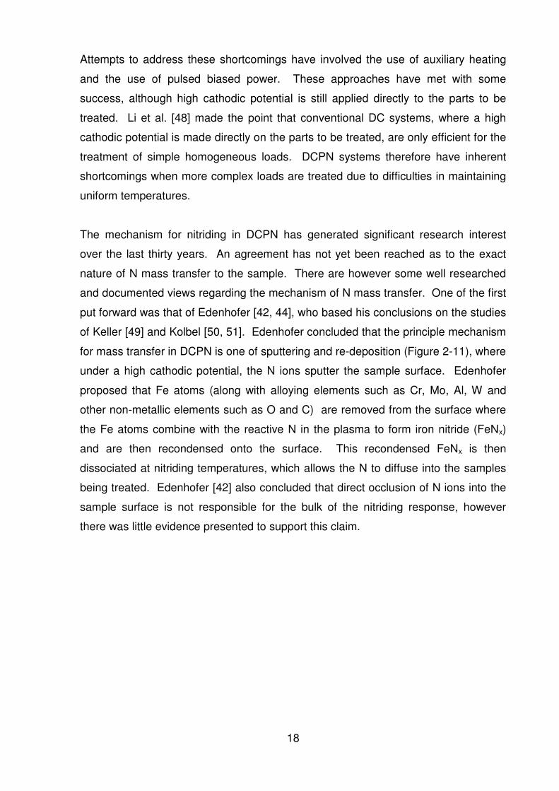
put forward was that of Edenhofer [42, 44], who based his conclusions on the studies
of Keller [49] and Kolbel [50, 51]. Edenhofer concluded that the principle mechanism
for mass transfer in DCPN is one of sputtering and re-deposition (Figure 2-11), where
under a high cathodic potential, the N ions sputter the sample surface. Edenhofer
proposed that Fe atoms (along with alloying elements such as Cr, Mo, Al, W and
other non-metallic elements such as O and C) are removed from the surface where
the Fe atoms combine with the reactive N in the plasma to form iron nitride (FeNx)
and are then recondensed onto the surface. This recondensed FeNx is then
dissociated at nitriding temperatures, which allows the N to diffuse into the samples
being treated. Edenhofer [42] also concluded that direct occlusion of N ions into the
sample surface is not responsible for the bulk of the nitriding response, however
there was little evidence presented to support this claim.

19
Figure 2-11: Proposed surface reactions and mechanism of mass transfer in ionitriding by
Edenhofer [42].
Hudis [52] proposed that there can only be two principal ionitriding mechanisms, gas
absorption and ionic bombardment. He devised a series of experiments to separate
these two potential mechanisms. In order to investigate the effects of gas absorption
on the nitriding response, Hudis immersed an electrically floating sample in an radio
frequency (RF) plasma and made the point that since there is no potential to sputter
surface Fe, then the sputter re-deposition model of Keller [49] and Edenhofer [42]
cannot in this case, be responsible for any nitriding response. Hudis concludes from
his tests on high tensile heat treated steels 4140 and 4340, that gas absorption is not
a significant contributor to the nitriding response, since the electrically floating sample
immersed in an RF plasma will not nitride to any significant degree. In the second
stage of his investigation, Hudis employed a mass and energy analyser attached to
the base of the cathode to identify the gas species and energy of the ions
bombarding the cathode. Based on this spectroscopy and the subsequent
metallurgical analysis, Hudis suggested that the most likely nitriding process was one
of ionic bombardment of N-H molecular ions (NH+, NH2+, NH3
+, N2H2+ etc) and not N
ions (N+, N2+). In addition, he concluded that N2 and H2 gases enabled superior

20
responses to those achieved with any mixture which included Ar. Additionally, he
admitted that it remained unanswered why N-H molecules produce a superior
nitriding response to N ions but alludes to the possibility that H had a positive affect
on cleaning the surface of the sample to allow penetration of dissociated N species.
Still in search for answers, 18 months later, Tibbets [53] conducted his own
experiments on pure Fe and a bright mild steel 1020. Tibbets also investigated the
species responsible for nitriding, focusing on the role of ions as opposed to neutral
species. Tibbets [53] devised an experiment to separate the nitriding response of
ions and the nitriding response of neutral species. Tibbets [53] used a temperature
controlled specimen holder (Figure 2-12) and applied +300 volts between the anode
and the grounded cathodic specimen to obtain a reference plasma nitrided sample
set.
Figure 2-12: Experimental apparatus employed by Tibbets [53] with the specimen serving as
the grounded cathode.
Tibbets [53] then installed a grid 1.5mm in front of the specimen surface (Figure
2-13) and connected it to ground to act as the new cathode within the system. To
repel the majority of positive incident ions, a +200 volt bias was then applied to the
specimen.

21
Figure 2-13: Experimental apparatus employed by Tibbets [53] for eliminating positive ions as
the nitriding species.
Tibbets then compared the response resulting from these experiments, he showed
that the responses in parts per million (ppm) N in Fe and ppm N in 1020 were
equivalent with or without the grid and therefore concluded, since the majority of
positive ions would be repelled due to the applied positive bias on the specimen, that
neutral species in his experiments were responsible for nitriding pure Fe and 1020
steel in a glow-discharge. He then devised an experiment to show the concentration
of nitriding species as a function of distance from a glow-discharge in an attempt to
measure the lifetime of the neutral nitriding species. In order to achieve this, two
metal screens were placed parallel to each other in a vacuum chamber and a DC
bias was applied between them to produce a glow-discharge (Figure 2-14). A tube of
1020 steel was then installed with a tungsten filament heater, while the rod remained
electrically floating. The rod and heater assembly was then placed perpendicular to
the screens and as close as possible without contact. Nitriding of the 1020 rod was
then performed for 3 hours at 550ºC. The 1020 rod was then sectioned and
analysed for its nitriding response. Tibbets asserted that a developed cathode fall
region is required in close proximity to the samples for a nitriding response to be
obtained. He also postulates from his results that Fe and steel are nitrided in a glow-
discharge principally by neutral species, particularly N atoms.

22
Figure 2-14: Experimental apparatus employed by Tibbets [53] for measuring active N
concentration gradient near a plasma discharge.
After one hour of nitriding at 516ºC, Tibbets [53] recorded a maximum dissolved N
content of ~7500 ppm. The method used to evaluate the concentration of N was
inert gas fusion, which measures the amount of N that evolves from the sample upon
fusion. Therefore, the measurement is from the whole sample and will average out a
N profile that peaked at the surface. Unfortunately surface and cross sectional
hardness measurements were not undertaken in Tibbets study and therefore the
nitriding response cannot be directly compared to the Hudis [52] study.
Owing to the difficulty in determining the mechanism of mass transfer in nitriding, yet
another alternative had been proposed. Brokman et al. [47], investigated the effects
of applying a crossed magnetic field to the ionitriding configuration of 304 stainless
steel tube (Figure 2-15).
Figure 2-15: Schematic of the experimental set-up employed by Brokman et al. [47].

23
Brokman et al. [47] postulated that under influence of a crossed magnetic field, the N
diffusion is sensitive to the applied current density. They proposed, contrary to
Tibbets [53], that having a net ion flux was responsible for the nitriding response
observed and not neutral species.
Brokman et al. [47] developed a theory based on the diffusion of vacancy-ion pairs
owing to the processes sensitivity to a reduction in the net ion current flow. This
theory suggests that under ionic bombardment, vacancies in the sample surface
were developed. The incident N ions could then combine with the vacancies to form
vacancy-ion pairs. Brokman et al. [47], suggest that the diffusion of these vacancy-
ion pairs into the bulk then takes place by vacancy substitutional diffusion which is
faster than interstitial N diffusion.
Answering the question of what is the mode of N mass transfer to the sample surface
is not simple. Recent investigations [54-57] have indicated in their studies that the
nitriding mechanism is a combination of different N mass transfer modes, where the
nitriding response is a cumulative sum of these alternative modes.
2.7 Post Discharge Nitriding
Given the limitations with DCPN mentioned above, several investigators have sought
a different approach. Most notably had been the study of Ricard et al. [7, 58] with
their development of post discharge nitriding (Figure 2-16).
Figure 2-16: A schematic of a post discharge nitriding reactor, as developed by Ricard et al.
[58].

24
Post discharge nitriding, as described by Ricard et al. [58] and Malvos et al. [59],
utilises a gap type microwave power generator (2.45GHz), commonly referred to as a
surfaguide to produce the plasma. According to Malvos [59], the plasma generated
in the quartz tube (Figure 2-16) remained in this position, while it is the role of the
flow of the process gas to transport the neutral excited species to the sample to be
treated. In a post discharge nitriding reactor, the samples to be treated are at an
electrically floating potential and are maintained at nitriding temperature by use of an
external heater (Figure 2-16). The samples are located 100 cm from the surfaguide
plasma generator and were embedded with a thermocouple.
Malvos et al. [59], based on the study of Ricard et al. [58], claimed that the species
that are mainly responsible for nitriding are atomic N since there is good correlation
between the N concentration in the surface and the atomic N density at the surface of
the sample. Malvos et al. [59] made the point that the mean gas velocity must be
sufficiently high enough so the neutral energetic N species do loose their kinetic
energy before they reach the sample surface. A more recent contribution to the
mechanism of nitriding in post discharge nitriding reactors was presented in Ricard et
al. [8], where it is shown by the use of optical emission spectroscopy that the nitriding
response of Fe based alloys in a post discharge nitriding reactor is due to N atoms
and not N2 molecules. In addition, Ricard et al. [8] found that there was a good
correlation between the nitrided layer thickness and the spatial distribution of N
atoms.
Cross sectional micrographs and X-Ray diffraction results presented by Ricard et al.
[58] showed that after a nitriding time of one hour that there is a significant nitriding
response for a 0.1% plain carbon steel. Although no surface and cross sectional
hardness measurements were undertaken, the post discharge nitriding technique
clearly demonstrates that a nitriding response can be achieved in the after glow
region of a microwave discharge where the active species are, according to Ricard
[58], neutral excited N. However due to variance in nitriding response relating to non
uniform workload temperature and geometries, post discharge nitriding was not
commercially successful [9] and therefore not commonly employed in industry.

25
2.8 Active Screen Plasma Nitriding
In recent years, an innovative Active Screen (Through Cage) Plasma Nitriding
(ASPN) system was developed [6]. ASPN has been the focus of much interest [9,
60, 61] since it claims to avoid fundamental problems associated with DC Plasma
Nitriding, these include a reduction of arcing damage and hollow cathode issues, and
most importantly, the ability to treat parts with a large range of geometries within the
one batch. Georges [9] the inventor of ASPN technology, took the innovative step of
applying the high cathodic potential to a screen surrounding the parts to be treated
which is the new cathode for the system, rather than directly on the load.
Samples are placed on the base plate which is enclosed by the large metal screen
made from expanded mesh. The base plate and samples to be treated are then
allowed to float or is subjected to a small negative bias of 100 to 200V [48]. The
rationale behind this innovation was the claim that the active species in plasma
nitriding were highly energetic neutrals [58] rather than ions and so there is no need
to form the plasma directly onto the parts to be treated. In this new technology the
role of the plasma generated on the active screen is as follows: (1) to heat up the
load by radiation thereby providing uniform temperature distribution throughout the
load and (2) to generate active neutral species.
Studies of ASPN technology have also been carried out by Li et al. [48] in a
laboratory scale system (Figure 2-17). Li et al. demonstrated in their laboratory
system (Figure 2-17), where the physical distance between the electrically floating
load and the active screen was of the order of 12mm, that the nitriding response of
low alloy steels was equivalent to DC plasma nitriding using a 500V DC bias without
the common problems of arcing damage, hollow cathode and edge effect.

26
Figure 2-17: A schematic of a laboratory based ASPN system employed by Li et al. [48].
On the basis of their results they went on to develop a compelling argument for
sputtering material from the active screen and deposition on to the samples as the
major mechanism by which N is transferred from the plasma to the solid surface. In
one of the first small scale laboratory studies of ASPN, Li et al. [48] demonstrated
that when the top lid of the active screen was made from copper that there was a
copper layer formed on the surface of the electrically floating samples. In addition,
when a titanium top lid was used, Li et al. [48] found titanium deposits on the
electrically floating sample surface. These results lead Li et al. [48] to the conclusion
that mass transfer occurs between the active screen and the samples. Further, since
the plasma is generated around the active screen and will be nitrided as in
conventional DCPN, then it is expected that iron nitride material from the active
screen will be transferred to the sample surface. It was therefore concluded that the
iron nitride active screen material deposited on the sample surface was responsible
for the nitriding response in ASPN. To support this theory, a parallel experiment was
conducted by Li et al. [48], where nitriding was undertaken with no active screen top
lid on electrically floating samples. The results revealed a two stage response on the
sample surface somewhat similar to the edge effects produced form DCPN
treatments. Firstly the area of the sample surface which was closest to the active
screen revealed a matt dark grey appearance and had a high nitriding response. On
the other hand, towards the centre of the sample surface which was farthest from the
active screen revealed the original metallic shined surface which although had a
significant surface hardness, it failed N diffusion case depth tests.

27
On the basis of a number of studies including that of Li et al. [48], Zhao et al. [62]
also concluded that the mechanism of mass transfer in ASPN involved sputtering of
iron nitride particles from the active screen. Based on these studies, Zhao et al. [62]
proposed a model for the mechanism of mass transfer in ASPN (Figure 2-18). This
model is an extension of the earlier model of Edenhofer [42] and clearly rests on the
key proposition that particles are sputtered from the active screen and deposited onto
the load. Zhao et al. [62] suggested that the iron nitride particles sputtered from the
active screen, physically and chemically adsorb active N atoms while passing
through the plasma space. The N rich particles are then randomly deposited on the
load. According to Zhao et al. [62], the physically adsorbed particles then dissociate
at the high substrate temperature resulting in diffusion of N into the steel. Based on
this model, Zhao et al. [62] concluded that sputtering of the sample surface, as
suggested by Edenhofer [42, 44], is not required since nitriding could be achieved by
having the samples in either cathodic potential (600-700V bias) (Figure 2-19a),
floating potential (Figure 2-19b) or grounded potential (Figure 2-19c).
Figure 2-18: Model proposed by Zhao et al. [62] for the nitriding mechanism in ASPN.

28
Figure 2-19: A schematic of the three laboratory based nitriding arrangements employed by Zhao et al. [62]. a) Sample at cathodic potential (DCPN), b) sample at floating potential, c)
sample at ground potential.
Ahangarani et al. [63] studied the effects of the open area fraction of the active
screen that surrounds the parts to be treated had on the nitriding response. In
addition Ahangarani et al. [63] studied the effect of replacing the top lid of the active
screen with an Fe plate. Similar to the study of Li et al. [48], the sample surface was

29
12 mm away from the active screen top lid [63] and utilised an experimental
apparatus comparable to that of Figure 2-17. It was found that [63], increasing the
size of the holes in the active screen had a positive affect on the nitriding response of
the electrically floating samples. While replacing the top lid of the active screen with
an Fe plate had a negative effect on the nitriding response. Ahangarani et al. [63]
attributed these results to the increased ease of transition of the active species
through the active screen holes toward the sample surface when the active screen
holes were larger. Conversely, replacing the active screen top lid with an Fe plate
restricted the active species.
Recently Alves et al. [64] compared the nitriding response between DCPN samples
treated with 500V bias [65] and electrically floating ASPN samples in the same
nitriding chamber which was similar to that shown in Figure 2-17. The distance from
the sample surface and the active screen top lid was less than 15 mm in the ASPN
experiments [64]. Alves et al. [64] showed that the DCPN samples had a non
uniformly nitrided surface due to edge effects. On the other hand, the ASPN
samples had a uniform matt grey surface finish after the nitriding treatment. After a
standard metallographic analysis, Alves et al. [64], concluded that the surface
hardness and composition of the ASPN samples were similar to that of the uniform
central area of the DCPN samples without the undesirable sample edge effects.

30
2.9 Summary
ASPN technology claims to have significant advantages over many of the
commercially available plasma based nitriding processes. The key innovation of
ASPN is the removal of the need to supply a high cathodic potential to the load. The
rationale behind this innovation rests on the claim that the mechanism of nitrogen
mass transfer is not ions, but either highly energetic neutrals [6, 9] or sputter
deposition [48] of the active screen material onto the samples. There is therefore no
requirement to form the plasma directly on the parts to be treated. Consequently, the
load is allowed to float or is subjected to a small negative bias potential. However,
there is debate as to the mechanisms for nitriding in ASPN [62]. In particular, are
energetic neutrals really the active species in ASPN, both at the laboratory and
commercial scale? Does sputtering of the active screen material on to the samples
play a role in the nitriding process? What level of bias is required on the load to get a
satisfactory response? Do the optimal nitriding parameters used depend on the load
type?
This project seeks to explore these and other issues in ASPN using a commercial
system manufactured and supplied by Georges, the director of Plasma Metal S.A. in
Luxembourg, Europe [6, 9] and in full scale operation at Surface Technology
Coatings (STC), a division of Sutton Tools Melbourne Australia.

31
Chapter Three
3 Experimental Techniques
The analytical techniques employed in this study are detailed in this chapter along
with their associated advantages and disadvantages. A description of the common
applications of the sample materials chosen for this study is introduced. Also
provided is a description of the metallographic techniques employed for sample
preparation prior to the nitriding treatments.
3.1 The materials investigated
Five steel grades were selected for this study because they are routinely nitrided to
improve their serviceability in a range of applications. The steel samples ranged in
composition from a plain carbon steel through to a relatively high alloy steel and are
described below with their compositions shown in Table 3-1 [48, 66].
P20 (M200, Plastic mould steel – quenched and tempered); Used extensively for
tooling in the injection moulding of plastic components, such as, automotive headlight
and taillight lenses. P20 is also used for general mechanical engineering
applications [66].
H13 (Hot work tool steel – in the as-received condition) and H13 (Hot work tool steel
– in the hardened and tempered condition, referred to in this study as HH13);
Commonly used for the manufacture of moulds for high pressure die casting of
aluminium, such as, automotive gearbox extension housings and bell housings.
Also, H13 is used extensively in the extrusion industries [66].
4140 (Pre heat treated nitriding steel); 4140 is the most commonly employed high
tensile steel for the manufacture of engine blocks, automotive gears, crankshafts,
steering components, connecting rods and other shafts and rods including
automotive axles. It is also used in the manufacture of conventional nuts and bolts
[66].

32
1020 (CS1020, Bright mild steel); This plain carbon steel is used for the manufacture
of general engineering components such as shafts, pins spindles, axles and small
gears and is readily weldable [66].
Silicon substrates (N Type, Phosphorus doped) were also employed in key
experiments because they are relatively inert and offer some insight into material
response to plasma nitriding under different treatment conditions. In addition, the Si
provided a non metallic substrate for the detection of metallic deposits.
Average Sample
Composition (wt%)
C Si Mn S Cr Mo P V Fe
P20 0.40 0.40 1.50 0.07 1.90 0.20 - - Bal
H13 0.39 1.00 0.40 - 5.10 1.30 - 1.00 Bal
4140 0.41 0.30 0.70 - 1.10 0.20 - - Bal
1020 0.18 0.10 0.30 0.04 - - 0.04 - Bal
Table 3-1: Average chemical composition of the steel substrates employed in this study [66].
The steel samples were sectioned from commercially available bar stock nominally
15 mm in diameter and 10 mm in thickness. Each sample was then given a standard
metallographic polish in four stages using a Struers polishing machine. These
stages consisted of polishing with 500, 1200, 2400 and 4000 grit silicon carbide
polishing paper until a smooth and uniform surface finish was obtained. The samples
were then immersed in a rust protective coating ready for the nitriding experiments.
Prior to the nitriding experiments, the samples were thoroughly cleaned in ethanol
and dried.

33
3.2 Plasma Etch
In selected experiments, plasma etching was carried out in situ prior to nitriding in
order to remove surface oxides on the substrates using a gas mixture of 50% H2 and
50% Ar at a pressure of 1.5 mbar. This was done for 30 minutes and was performed
at a substrate temperature of 520ºC.
3.3 Active Screen Plasma Nitriding (ASPN) system and conditions
The ASPN system used in this project is shown in Figure 3-1 and schematically in
Figure 3-2. The ASPN system is based on patented technology [6] and is currently
installed, and under commercial operation at STC.
Figure 3-1: The ASPN system as installed at STC.

34
Figure 3-2: A schematic of the ASPN system.
Each automated treatment within an ASPN nitriding cycle consisted of up to ten
separate steps with implicit temperature ramps and holds, selectable gas mixtures,
treatment pressures and bias voltages. Note that the heat up time was
approximately 3 hours for a standard nitriding cycle.
The nominal base pressure prior to commencement of the nitriding cycle was 4 x 10⁻²
mbar. At the beginning of selected treatments, a pre nitride plasma etch was used to
clean the steel substrate surfaces of oxides (as described in section 3.2). During
nitriding, the temperature was controlled by automatically varying the power supplied
to the active screen since radiation from the active screen, that is from the glow-
discharge around the active screen, heats the load and base plate. The temperature
was monitored using an isolated K type thermocouple mounted in a dummy sample
on the base plate and controlled by automatically varying the power supplied to the
active screen. Treatment gases were supplied via mass flow controllers. The
treatment gas enters the chamber via a gas conduit at the top of the furnace and is
pumped out of the chamber at the bottom. Once a nitriding treatment was
completed, the nitriding system was back filled with N2 and cooled using a fan
located in the top of the chamber.
The nitriding experiments were carried out at a specific gas mixture, with a fixed bias
voltage which corresponded to a constant current setting. The bias power supply
was controlled via a potentiometer on the control panel (Figure 3-2). This

35
potentiometer setting determined the constant current output of the bias power
supply and remained fixed at its value for the duration of the nitriding cycle.
The base plate in the ASPN system was 1200 mm in diameter and had a central hole
of 200 mm diameter, while the active screen was of a cylindrical shape with a top lid
made from the same mesh material as the active screen and was 1300 mm in
diameter and 1600 mm tall (Figure 3-3).
Figure 3-3: The active screen used in the ASPN system.
3.4 The bias power supply
The power supply for the bias in the ASPN system was an Electronavale
technologies product and had a maximum output power of 15 KW. The unit was a
current controlled power supply and was a pulsed DC type operating at 500Hz.
During the negative pulse, a higher frequency waveform was superimposed at ~5kHz
as described in detail below. When the bias power supply was switched off the base
plate was at a floating potential. The bias setting control was a variable

36
potentiometer, with graduations of 5 percent (%). Once a setting was selected and
the treatment begun the bias power supply outputs a constant current and remained
fixed for the duration of the nitriding treatment. The power supply signal varied with
the bias setting according to Figure 3-4. Note that these measurements were
undertaken with no workload in the ASPN system.
Figure 3-4: The voltage waveforms of the bias power supply used in the ASPN system at various bias settings. Note that the heavy black line in all of the figures represents the
grounded zero line. a) 7% bias (200V/Div, 0.5mS/Div), b) 16% bias (100V/Div, 0.5mS/Div), c) 30% bias (200V/Div, 0.5mS/Div), d) 40% bias (200V/Div, 0.5mS/Div).

37
It can be seen that the power supply signal changes shape as the bias setting
changes. The frequency remained fixed, however the pulse shape varies. At 7%
bias, the high frequency peaks are of the order of ~820V, and are reduce to ~580V at
16% bias. At 30% and 40% bias, the high frequency peaks are of the order of
~1250V and ~1400V respectively (Table 3-2). Additionally the widths of the negative
pulses are reduced for the 16% and 40% bias cases. With the increase in bias
setting the signal shifts more negative with the root mean square (RMS) voltage
value displayed on the control panel of the ASPN system. The RMS values are
shown in Table 3-2, where the RMS voltage value increases as the bias setting was
increased.
Bias Setting Current (A) Peak (V) RMS (V)
7% ~2 ~820 ~239
16% ~5 ~580 ~312
30% ~9 ~1250 ~520
40% ~12 ~1400 ~591
Table 3-2: Table showing the current, peak and RMS voltages for the different bias settings using a 25% N2, 75% H2 gas mixture and no workload.
3.5 Temperature control and the Active Screen Power supply
During each phase in the nitriding cycle, the temperature was monitored and
controlled by the control panel in a feedback configuration. The temperature was
automatically varied by changing the power supplied to the active screen as radiation
from the active screen and the glow-discharge around the active screen heat the load
and base plate. The temperature was monitored by an isolated K type thermocouple
mounted in a dummy sample on the base plate.
3.6 Hardness Response
In industry the nitriding response in terms of surface hardness is usually measured
using a Superficial Rockwell hardness tester. In this investigation, both the surface
hardness and hardness profiles were measured using a Vickers microhardness
tester. This is time consuming and labour intensive but is essential to accurately
evaluate the nitriding response of a sample.

38
3.6.1 Surface Hardness Measurements
The microhardness indenter system located at the Industrial Microscopy Laboratory
at Swinburne University of Technology, Faculty of Engineering and Industrial
Sciences was employed to perform indentation hardness measurements on the
surface of the nitrided samples. The microhardness tester employed was a
Shimadzu type m tester with a Vickers diamond pyramid indenter. The indenter was
a ground square pyramid with a known angle of 136 degrees between its opposing
faces (Figure 3-5).
Figure 3-5: Vickers pyramid diamond indenter schematic.
Once an indentation was made on the surface of the sample to be tested, the Vickers
Hardness Value (HV) was obtained. The HV is a function of both diagonals d1, d2
and the applied load. The HV is the applied load in grams divided by the surface
area of the indentation in mm2. Hence,
.2
136sin2
2
0
d
F
HV
=
Where,
HV = Vickers hardness value.
F = the applied load on the diamond indenter.
d = the arithmetic mean in mm of the two diagonals d1 and d2, according to,
.2
21dd
d+
=
In all of the work presented in this thesis, the applied load on the diamond indenter
was 100g for duration of 15 seconds. The two diagonals d1 and d2 were measured

39
by using the ocular microscope with an inbuilt ocular micrometer. To obtain
statistically valid results, each sample was subjected to a series of five surface
indentations before an average surface HV was obtained. The HV obtained from
these measurements were then compared to the HV obtained from the same sample
material before the nitriding treatment to gauge an increase in the surface hardness
due to nitriding.
3.6.2 Cross Sectional preparation and Hardness Measurements
In order to obtain hardness profiles of the nitrided samples, the latter were first
sectioned using a slitting saw. The samples were water cooled to ensure
overheating did not occur during sectioning. They were mounted in an appropriate
Bakelite compound using a LECO mounting press to ensure edge retention and
stability during microhardness testing. The mounted samples were then polished in
four stages using the same Struers polishing machine. The technique of polishing
was the same as that of the surface polish i.e. 500, 1200, 2400 and 4000 grit silicon
carbide polishing paper until a smooth and uniform surface finish was obtained
(Figure 3-6).
Figure 3-6: A sample mounted in Bakelite and polished in cross section.
The technique of obtaining data points of HV in the cross section was similar to that
of obtaining surface HV. Deformation of the sample under cross sectional
microhardness testing restricts the proximity of indentation close to the nitrided
surface in cross section.

40
3.7 Glow-Discharge Optical Emission Spectroscopy
Glow-Discharge Optical Emission Spectrometry (GD-OES) (Figure 3-7) was used to
evaluate the concentrations of N, O and various alloying elements present in the
surface of the nitrided samples. In this study, elemental depth profiles were
measured using a LECO GDS-850 GD-OES system with a 4mm copper anode. GD-
OES has been shown to be a powerful analytical tool to evaluate both the presence
and quantity of various elements in the surface of solids [67, 68]. To obtain
meaningful quantification data, it is important to calibrate the GD-OES system using
certified standards. Sputter rates were calibrated with a database which was
provided by the manufacturer which were checked against depth standards. A daily
drift correction was also undertaken to rectify any errors present in the optical system
of the GD-OES means of a series standards [69].
Figure 3-7: The Glow-Discharge Optical Emission Spectrometer employed in this study. Insert
shows the sample loaded into place.
In GD-OES, the sample under test (Figure 3-7) acts as the cathode of the system
while the anode, separated from the cathode by an insulating rubber ring, consists of
a thin metal tube (Figure 3-8). Once evacuated, an Ar glow-discharge was produced
between the cathode and the anode. The positively charged Ar species are
accelerated toward the sample surface where uniform surface sputtering of the
sample takes place. The sputtered particles are then excited in the Ar plasma by
collisions with other gaseous species. The ionised atoms then de-excite to their
ground state and are analysed using optical emission spectroscopy [69].

41
Figure 3-8: Cross sectional schematic of the Glow-Discharge configuration.
By utilising the fact that each element has its own unique atomic emission spectrum,
the composition of an unknown sample may be identified by comparing the atomic
spectrum obtained from the sample to the elements in the spectral database [70].
3.8 Electron Microscopy
Electrons are used as the illuminating source in electron microscopy in order to
achieve high resolution imaging and analysis of samples. By using electrons instead
of visible light as the illuminating source for imaging allows nano-sized characteristics
to be observed. Electrons of a high energy exhibit wave like properties where the
associated wavelength of electrons is much smaller than that of visible light. It is this
characteristic that enables electrons to provide high resolution images, using the two
main instrument types: Scanning Electron Microscopy (SEM) and Transmission
Electron Microscopy (TEM).
3.8.1 Scanning Electron Microscopy
The SEM has an electron gun which produces a beam of electrons. This beam is
manipulated and focused by a series of coils along the path of the electrons. By
using the magnetic field produced from these coils, the electron beam is rastered in a
rectangular line by line fashion over an area of interest on the sample surface. The
electrons interact with the sample surface, generating amongst other things,
secondary electrons (SE). The SE’s escape from the sample surface and are
detected by a suitable electron detector. Since the energy associated with SE’s is
low, it is only the SE’s generated near the surface of the sample that are detected. In
addition, electrons in the primary beam can be backscattered, loosing only a fraction
of their energy. These backscattered electrons can also be used for imaging. The
topography of the sample surface determines the amplitude of the electron signal

42
detected. Compositional information can also be obtained by analysis of the emitted
characteristic X-Rays which are generated within the interaction volume as ionized
atoms relax.
In this study, two SEM’s were used for imaging the samples. The first was a Zeiss
Supra 40, variable pressure field emission electron source microscope located at the
Industrial Microscopy Laboratory at Swinburne University of Technology. The
second was a Philips XL-30 electron microscope with a conventional electron source
located at the Microscopy and Microanalysis facility, Royal Melbourne Institute of
Technology (RMIT).
Sample surface SEM images were obtained with minimal sample preparation, while
cross sectional scanning electron microscopy (XSEM) images were obtained after
prior etching with 2% nitric acid in ethanol.
3.8.2 Transmission Electron Microscopy
Transmission Electron Microscopy (TEM) was used to examine the microstructure of
the Si test substrates used in this study. The TEM analysis presented in this study
was performed using a JEOL 2010 TEM operating at 200 kV.
In addition, Energy Dispersive Spectroscopy (EDS) and Electron Energy Loss
Spectroscopy (EELS) was used to determine the atomic composition of the sample
under investigation. EDS was used for quantitative analysis of the elements
contained within the sample by analysing the emitted characteristic X-Rays from the
sample, while EELS utilises the characteristic energy losses of the primary electron
bean after interacting with the sample. A full descriptive analysis of TEM and its
operation can be found in Williams and Carter [71].

43
3.8.2.1 Cross Sectional TEM
To analyse the nitrided Si substrates treated in the ASPN system, significant sample
preparation had to be undertaken. Cross sectional TEM (X-TEM) sample preparation
required the Si substrate to be cleaved into thin sections prior to the assembly of a
physically stable sample group (Figure 3-9a) which could then be polished. The
polishing technique consisted of a mechanical stage followed by ion beam thinning.
Figure 3-9a was thinned down to Figure 3-9b by first polishing with diamond lapping
pads until the thinnest section of the wedge was optically transparent. The sample
was then placed on a copper grid and mounted in an ion beam thinner (GATAN Dual
Ion Mill model 600) and Precision Ion Polishing systems (PIPS), (GATAN model 691)
to obtain a wedge section (Figure 3-9b) that was transparent to the primary electron
beam in the TEM.
Figure 3-9: A schematic of the sample preparation arrangement used for XTEM analysis.
A) Shows the sample group after construction, B) Shows the sample group after cross sectional polishing, where the thin point of the wedge was the area used for TEM
imaging.

44
3.8.2.2 Energy Filtered TEM
Energy Filtered TEM (EFTEM) was performed using a Gatan Imaging filter attached
to the bottom of the TEM. EFTEM was used to generate a map of one particular
element by choosing the appropriate parts of the EELS spectrum. An elemental map
can be generated since the EELS spectrum contains the chemical signature of the
elements that were present in the sample.
3.9 X-Ray Diffraction
X-Ray Diffraction (XRD) is a powerful technique that can produce crystallographic
information about materials [72], through elastic scattering of X-Rays or diffraction,
from within the sample. By comparing the diffraction spectra with a database
containing the diffraction data from known materials, the sample structure can be
identified.
Structure analysis undertaken using XRD was used to determine the phases present
in the nitrided steels. XRD was performed directly on the substrates that were
mounted inside the XRD apparatus. Detailed information on XRD can be sourced in
various texts such as Cullity [72]. In this study, XRD was performed on a Bruker D8
ADVANCE Powder Diffractometer , using Ni-filtered copper Kα radiation (λ
=1.5406Å), a typical spectrum was obtained under the following conditions: 2θ range
30-100°, step size 0.02°, count time 5s step-1, temp 25°C (room) and analysed using
the software package Diffrac Plus Release 2001.

45
Chapter Four
4 Characterisation of the commercial ASPN system
Just prior to the start of this project it was found that the commercial ASPN system
located at STC required a bias during the nitriding treatment in order to perform
satisfactorily for a range of load types. Therefore, in order to understand the ASPN
system in detail, a series of experiments were devised to reveal the effects of the
main treatment variables on the nitriding response. In addition, any interaction
between treatment variables was important in understanding how combinations of
these parameters influence the nitriding response. Therefore, design of experiments
[73] was employed so that the role of each variable could be evaluated and any
interaction between them determined.
4.1 Overview of ASPN system operation
A typical ASPN treatment consisted initially of loading the samples onto the base
plate. The chamber was then closed and pumped down to a nominal base pressure
of 4 x 10⁻² mbar. On reaching this pressure, mass flow controllers allowed H2 to
enter the ASPN chamber up to a pressure of 0.75 mbar. In the early stages of this
phase of the treatment, the active screen power supply was switched on, generating
a plasma around the active screen thereby heating the chamber and the workload to
the set point temperature (typically 520ºC). A K type thermocouple was mounted in a
dummy sample on the base plate and the electrical feedback regulated the power
supplied to the active screen to control the chamber temperature. This step took
approximately 180 minutes to allow for temperature stabilisation of the workload.
Once the ASPN chamber was stable at 520ºC, a plasma etch can be employed to
help remove surface oxides from the substrates. If a plasma etch was selected, the
mass flow controllers allowed the treatment gas (typically a mixture of 50% Ar, 50%
H2) into the chamber to a pressure of 1.5 mbar. In the present study, this was set at

46
30 minutes. The power supplied to the base plate to initiate plasma etching was
determined by the bias setting control knob.
At the completion of the plasma etch, or at the end of the heating stage if the plasma
etch was not selected, the nitriding cycle was initiated. The bias setting was again
used to control the level of power supplied to the base plate and workload during the
nitriding cycle. The treatment gases (N2 and H2) were then allowed into the chamber
and regulated to a chamber pressure of 2 mbar. The gas mixture ratio was
predetermined and selected by the operator prior to the commencement of the
nitriding cycle. The nitriding cycle was run for 360 minutes at a temperature of
520ºC.
This was followed by the cool down stage in which the active screen and bias power
supplies were switched off and the chamber back filled with N2 gas to a chamber
pressure of 0.9 bar. To assist with the cooling, a large circulation fan was used and
the chamber was vented when the thermocouple reached room temperature.
4.2 The effect of bias and etching on the nitriding response
The first stage for this set of experiments consisted of a randomised full factorial
experimental design [73] of 2 factors at 2 levels across four steels, P20, H13, 4140,
1020. The two factors were the bias setting and the pre-nitride plasma etch (Table
4-1). The treatment gas mixture selected was 50% N2, 50% H2. The bias setting
was selected from practical experience to be at a level that resulted in an acceptable
nitriding response as measured with a Superficial Rockwell hardness tester for the
selected steels. The bias was set at 30% which corresponded to a constant bias
current of ~ 9A (Table 4-2).

47
Treatment A (Bias)
B (Etch)
AB
1: Bias on, Etch on +1 +1 +1 2: Bias on, Etch off +1 -1 -1 3: Bias off, Etch on -1 +1 -1 4: Bias off, Etch off -1 -1 +1
Table 4-1: Experimental design for the two factors, bias and etch, and their interaction in
column AB. High levels (+1) are ON, low levels (-1) are OFF.
The bias and etch on and off states were structured according to Table 4-1 and the
indicated values for the treatment parameters of current and voltage are shown in
Table 4-2. Four separate treatment were carried out, each of these at a fixed
chamber pressure, treatment gas mixture and temperature. The rest of the treatment
parameters for each of the four nitriding cycles conducted in this series of
experiments are detailed in Table 4-3.
Etch Step Nitride Step Treatment Iscreen
(A) Vscreen
(V) Iwork (A)
Vwork (V)
Iscreen (A)
Vscreen (V)
Iwork (A)
Vwork (V)
1: Bias on, Etch on 61 351 9 345 42 406 9 458 2: Bias on, Etch off - - - - 72 413 9 407 3: Bias off, Etch on 69 355 9 334 101 457 - - 4: Bias off, Etch off - - - - 102 440 - -
Table 4-2: Indicated values for the current and voltages for each treatment. Note that the bias
for the workload (Vwork) is the RMS value.
Treatment Parameter
Step 1 (Heat up)
Step 2 (Etch)
Step 3 (Nitride)
Step Time (min) ~180 30 360 Pressure (mbar) 0.75 1.5 2.0
Gas Mixture 100% H2 50% Ar, 50% H2 50% N2, 50% H2 Bias OFF OFF or ON OFF or ON
Temp (°C) 520 520 520
Table 4-3: Table showing the range of treatment parameters. Step 1 was a heat up from room temperature. At the end of step 3 the chamber was back filled with N2 to approximately 0.9 bar
and fan cooled.

48
4.2.1 Results and Discussion
4.2.1.1 Surface Hardness
Figure 4-1 shows the 95% Confidence Interval (CI) for the treatment mean where the
confidence Level α was 0.05 and the number of degrees of freedom was four for the
t-test. The surface harness values were obtained using the Shimadzu
microhardness tester as described in Chapter 3. The magnitude of hardness
increase above the as-received hardness is related to the alloy composition of the
steel [16, 74, 75]. Table 4-4 details the weight percentage of the strong nitride
forming elements in the steels investigated. Figure 4-1 can be interpreted on the
basis that the strong nitride forming elements give rise to greater precipitation of alloy
nitrides leading to an increased hardening response. Using the values in Table 4-4,
the magnitude of the hardening response is expected to be greatest for H13 and the
least for 1020.
0
200
400
600
800
1000
1200
1400
P20 H13 4140 1020Material
Su
rface H
ard
ness (
HV
/0.1
)
Etch + Bias Bias Only Etch Only No Bias No Etch As-Received
Figure 4-1: Effect of nitriding treatments on the surface hardness for the selected steels.
P20 H13 4140 1020
4 8.8 2.3 0.4
Table 4-4: The proportion (wt%) of the strong alloy nitride forming elements (Mn, Cr, Mo, V)
present in P20, H13, 4140 and 1020 steels [66].

49
Using the 95% CI for the estimation of the population mean of surface hardness
(Figure 4-1) allows ‘on the fly’ hypothesis testing for the individual treatments. It is
clear from these results that the bias appears to have a significant influence on the
nitriding response. An Analysis of Means (ANOM) allows a visual de-coupling of the
factor effects (bias and etch) and the results are shown in Figure 4-2. It is evident
that only factor A (Bias) is significant for all the steels, whereas only H13 shows the
main effect of factor B (Etch). As a guide to the interpretation of Figure 4-2 the
longer (steeper) the line the more effect a factor has, Analysis of Variance (ANOVA)
formalises this.
-300
-200
-100
0
100
200
300
P20 A
-1
P20 A
+1
H13
A-1
H13
A+1
4140
A-1
4140
A+1
1020
A-1
1020
A+1
P20 B
-1
P20 B
+1
H13
B-1
H13
B+1
4140
B-1
4140
B+1
1020
B-1
1020
B+1
Material and Factor Level
Hard
ness D
evia
tio
n (
HV
/0.1
)
Effect of the Bias Effect of the Etch
MS Screen
Figure 4-2: Analysis of Means (ANOM) for the deviation from the overall treatment mean of surface hardness by material for the main factors A & B.
The ANOM (Figure 4-2), for the deviation of treatment surface hardness from the
overall material surface hardness shows the main factor effects i.e. exclusive of the
other factor. The overall surface hardness is a linear superposition of the bias
response and etch response. Superposition can be applied to the results because a
full factorial experiment design was used, i.e. the factors are balanced and
orthogonal, and because the ANOM explicitly separates the factor effects.

50
4.2.1.2 Cross Sectional Hardness Profiles
A Vickers indent samples more than the surface and assumptions are made as to the
hardness depth profile. A cross sectional hardness profile provides additional bulk
and near surface analysis to further characterise the nitriding response. The cross
sectional hardness depth profiles were obtained for each of the four steels and are
shown in Figure 4-4. To estimate the uncertainties associated with the cross
sectional hardness results presented throughout this thesis, a series of hardness
profiles were measured on one sample (P20, bias and etch). The five cross sectional
hardness depth profiles are shown in Figure 4-3 along with the mean and the 95% CI
indicated by the error bars.
0
200
400
600
800
1000
1200
0 50 100 150 200Depth (microns)
HV
(0
.1)
Set 1
Set 2
Set 3
Set 4
Set 5
Mean
As-Received
Figure 4-3: The results and uncertainties of the hardness depth profiles as measured on one
sample (P20, bias and etch) five times.
This analysis can be used to provide an estimate of the uncertainty associated with
determining the case depth (as defined in section 2.1) from a cross sectional
hardness profile. Using the results of Figure 4-3, the mean case depth was 110 ±
5µm. Case depths were only calculated when a hardness increase of at least 200
HV points above the as-received HV in a particular profile was obtained.

51
0
200
400
600
800
1000
1200
0 50 100 150 200Depth (microns)
HV
(0.1
)
Etch + Bias
Bias Only
Etch Only
No Bias No Etch
As-Received
P20
0
200
400
600
800
1000
1200
0 50 100 150 200Depth (microns)
HV
(0.1
)
Etch + Bias
Bias Only
Etch Only
No Bias No Etch
As-Received
H13
0
200
400
600
800
1000
1200
0 50 100 150 200Depth (microns)
HV
(0.1
)
Etch + Bias
Bias Only
Etch Only
No Bias No Etch
As-Received
4140
0
200
400
600
800
1000
1200
0 50 100 150 200Depth (microns)
HV
(0.1
)
Etch + Bias
Bias Only
Etch Only
No Bias No Etch
As-Received
1020
Figure 4-4: Hardness depth profiles for all four treatments.

52
It is clear from the cross sectional hardness profiles that the bias had a large effect
on the nitriding response. The bias on/etch on and bias on/etch off treatments in
Figure 4-4 are not significantly different when the errors associated with performing a
hardness depth profile are taken into consideration. Similarly the bias off/etch on and
bias off/etch off treatments in Figure 4-4 are not significantly different except for the
H13 steel and to a lesser extent at the surface of the P20 steel. In order to quantify
the differences in the hardness profiles, the values of case depths, according to the
definition given in section 2.1, are shown in Table 4-5. The case depth is high for
P20, H13 and 4140 for the bias on/etch on and bias on/etch off treatments. In the
case of 1020, the response was subtle with a slight increase in hardness above the
as-received condition over the first 200µm.
Treatment / Material P20 H13 4140 1020 1: Bias on, Etch on 105 85 130 N/A 2: Bias on, Etch off 100 80 110 N/A 3: Bias off, Etch on N/A 15 N/A N/A 4: Bias off, Etch off N/A N/A N/A N/A
Table 4-5: Case depth values in µm for all four treatments and selected steels.
Overall there is a large response of the hardness to bias on and a negligible effect to
etch on. However a visual analysis is more complicated than comparing individual
curves as doing this encapsulates both of the bias and etch factors. It is not possible
to visually de-couple the factor effects. In addition, the hardness profiles (Figure 4-4)
are material dependent, supporting the surface hardness results (Figure 4-1). H13
displays the largest hardness increase in cross section, followed by P20, 4140 and
1020. This result agrees with the discussion earlier (page 48) which related the
concentration of strong alloy nitride forming elements with an increased hardening
response. Interestingly, the depth of hardening is also material dependent, where
the case depth for the P20 and 4140 steels is greater than H13 while for 1020 the
hardening response is minor. This suggests that with an increase in strong alloy
nitride forming elements, the magnitude of the hardening response is larger while the
depth of hardening is reduced. In addition, a steel that has a low concentration of
strong alloy nitride forming elements, 1020 for example, presumably gives rise to a
greater depth of diffusion of interstitial N (less than 0.1 wt%) but not enough super-
saturation of N in solid solution to give rise to a large hardening response.

53
4.2.1.3 Glow-Discharge Optical Emission Spectroscopy
The corresponding N wt% depth profiles for the four steels are shown in Figure 4-5.
02468
10121416
0 2 4 6 8 10Depth (microns)
N (
wt
%)
Etch + BiasBias OnlyEtch OnlyNo Bias No EtchAs-Received
P20
02468
10121416
0 2 4 6 8 10Depth (microns)
N (
wt
%)
Etch + BiasBias OnlyEtch OnlyNo Bias No EtchAs-Received
H13
02468
10121416
0 2 4 6 8 10Depth (microns)
N (
wt
%)
Etch + BiasBias OnlyEtch OnlyNo Bias No EtchAs-Received
4140
02468
10121416
0 2 4 6 8 10Depth (microns)
N (
wt
%)
Etch + BiasBias OnlyEtch OnlyNo Bias No EtchAs-Received
1020
Figure 4-5: N wt% depth profiles from GD-OES (LECO GDS-850, 4mm Cu anode).

54
The bias had a very large effect on the hardness (Figure 4-4) and the N depth
profiles (Figure 4-5) regardless of the etch condition. When the bias is off, the etch
on parameter had a noticeable effect on the N depth profiles (Figure 4-5) especially
near the surface in comparison to the etch off case. The comparison between the
hardness profiles (Figure 4-4) and the GD-OES profiles (Figure 4-5) appear to be
contradictory, however, fundamental limitations such as surface deformation and
edge retention in testing restricts the proximity of hardness measurements close to
the edge of the sample. Therefore comparisons between the hardness profiles and
the GD-OES profiles can only take place with a consideration of the horizontal axis
scales. To further characterise the GD-OES profiles, Table 4-6 details the peak N
concentrations and the N concentration at a depth of 10 µm for all four steels and
treatment conditions. The values indicate that the bias parameter had a large effect
on the N concentration. The N concentration at 10µm gives an indication of the
response seen in the hardness depth profiles (Figure 4-4). It can be seen that there
is a good correlation between the N concentration at 10µm and the level of hardness.
This effect can be understood by reviewing the Fe-N phase diagram (Figure 2-1),
where an interstitial N concentration larger than 0.1 wt% in the α-Fe matrix results in
the precipitation of γ’- Fe4N iron nitride. This precipitation of γ’- Fe4N is responsible
for some of the hardening response observed in Figure 4-4.
Peak N wt% N wt% at 10µm Peak N wt% N wt% at 10µm Treatment / Material P20 H13
Bias + Etch 12.8 1.5 15.3 2.4 Bias Only 11.2 1.3 13.3 2.1 Etch Only 1.9 0.3 3.6 0.6
No Bias No Etch 1.1 0.2 3.6 0.1 4140 1020
Bias + Etch 13 0.7 11 0.2 Bias Only 13.5 0.6 11.6 0.2 Etch Only 2.4 0.2 0.8 0.1
No Bias No Etch 1 0.1 0.5 0.05
Table 4-6: Tabulated values from Figure 4-5 showing the concentration of N in wt% at the peak and at 10µm.
In addition to the N depth profiles, O depth profiles for H13 are shown in Figure 4-6
and are representative of the O concentrations for the other steels. The results of
Figure 4-6 show that the O concentration for the no bias/no etch treatment condition
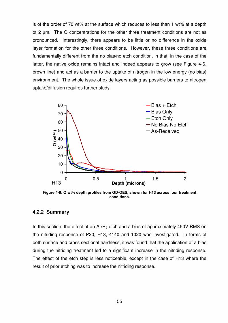
55
is of the order of 70 wt% at the surface which reduces to less than 1 wt% at a depth
of 2 µm. The O concentrations for the other three treatment conditions are not as
pronounced. Interestingly, there appears to be little or no difference in the oxide
layer formation for the other three conditions. However, these three conditions are
fundamentally different from the no bias/no etch condition, in that, in the case of the
latter, the native oxide remains intact and indeed appears to grow (see Figure 4-6,
brown line) and act as a barrier to the uptake of nitrogen in the low energy (no bias)
environment. The whole issue of oxide layers acting as possible barriers to nitrogen
uptake/diffusion requires further study.
0
10
20
30
40
50
60
70
80
0 0.5 1 1.5 2Depth (microns)
O (
wt%
)
Bias + EtchBias OnlyEtch OnlyNo Bias No EtchAs-Received
H13
Figure 4-6: O wt% depth profiles from GD-OES, shown for H13 across four treatment conditions.
4.2.2 Summary
In this section, the effect of an Ar/H2 etch and a bias of approximately 450V RMS on
the nitriding response of P20, H13, 4140 and 1020 was investigated. In terms of
both surface and cross sectional hardness, it was found that the application of a bias
during the nitriding treatment led to a significant increase in the nitriding response.
The effect of the etch step is less noticeable, except in the case of H13 where the
result of prior etching was to increase the nitriding response.

56
4.3 Effect of bias on the nitriding response
Given the magnitude of the difference between the nitriding response for the bias on
and bias off conditions in the preceding section, it was decided to investigate the
level of bias required to obtain a satisfactory nitriding response in ASPN. These
experiments consisted of a series of nitriding treatments where the bias setting was
varied between the two points of the preceding section, namely bias off at 0% and
bias on at 30%. The nitriding treatments were conducted on P20 and H13 steels
using a gas mixture of 25% N2, 75% H2 at bias settings of 0%, 7%, 10%, 20% and
30%, where the measured current and voltage values are shown in Table 4-7 for
both the active screen and the base plate. The experiments in this section all had a
pre-nitride plasma etch, except treatment 1 as shown in Table 4-7. This was used as
a reference in this study.
Etch Step Nitride Step Treatment
Iscreen (A)
Vscreen (V)
Iwork (A)
Vwork (V)
Iscreen (A)
Vscreen (V)
Iwork (A)
Vwork (V)
1: 0% Bias off, Etch off
- - - - 106 481 - -
2: 0% Bias off, Etch on
85 381 9.2 344 101 483 - -
3: 7% Bias on, Etch on
101 409 0.5 163 104 466 0.55 205
4: 10% Bias on, Etch on
103 404 1.7 170 105 476 1.8 257
5: 20% Bias on, Etch on
92 398 5.7 261 90 467 5.6 378
6: 30% Bias on, Etch on
77 370 9.1 340 63 453 9.3 540
Table 4-7: Indicated values for the current and voltages for each treatment. Note that the bias
for the workload (Vwork) is the RMS value.
Six separate treatments were carried out, each of these at a fixed chamber pressure,
treatment gas mixture and temperature (see Table 4-8). The bias setting was varied
as per the schedule shown in Table 4-7, where the indicated current values for the
etch step varied accordingly with the bias setting.

57
Treatment Parameter
Step 1 (Heat up)
Step 2 (Etch)
Step 3 (Nitride)
Step Time (min) ~180 30 360 Pressure (mbar) 0.75 1.5 2.0
Gas Mixture 100% H2 50% Ar, 50% H2 25% N2, 75% H2 Bias OFF VARIABLE VARIABLE
Temp (°C) 520 520 520
Table 4-8: Table showing the range of treatment parameters. Step 1 was a heat up from room temperature. At the end of step 3 the chamber is back filled with N2 to approximately 0.9 bar
and fan cooled.
4.3.1 Results and Discussion
4.3.1.1 Surface Hardness
Figure 4-7 shows the 95% CI for the treatment mean where the confidence level α is
0.05 and the number of degrees of freedom was four for the t-test.
0
200
400
600
800
1000
1200
1400
P20 H13Material
Su
rfa
ce
Ha
rdn
es
s (
HV
/0.1
)
As-Received 0V Etch / 0V Bias 344V Etch / 0V Bias163V Etch / 205V Bias 170V Etch / 257V Bias 261V Etch / 378V Bias340V Etch / 540V Bias
Figure 4-7: Effect of bias setting on the surface hardness for two steels, P20 and H13.
The results give an indication of the level of bias setting that is required to have an
effect on the uptake of N such that a sufficient hardening response is obtained. The
surface hardness is significantly increased above that of the as-received P20
substrate hardness for the 378V and 540V bias cases. However, there still exists a
large separation between these two cases where there is over 100 point’s difference
in the surface hardness after considering the 95% CI. In contrast, for H13 the
responses for biases above and including 257V are similar. Interestingly, H13 shows

58
a significant increase in surface hardness without a bias. This can be attributed to
the strong alloy nitride forming elements that are in higher concentrations in H13 in
comparison to P20. In addition, the surface hardness results shown in Figure 4-7
suggest that P20 may benefit, in terms of surface hardness, by an even higher bias
voltage, although this would of course defeat the intended purpose of using ASPN,
i.e. applying little or no bias. Furthermore, H13 seems to have achieved saturation in
surface hardness at 257V. Based on the surface hardness results alone, it may be
concluded that this commercial ASPN system can produce a nitriding response, at
least in H13, using a small negative bias of a few hundred volts.
4.3.1.2 Cross Sectional Hardness Profiles
The cross sectional hardness profiles for P20 and H13 substrates nitrided at the
different bias settings are shown in Figure 4-8.
0
200
400
600
800
1000
1200
0 50 100 150 200Depth (microns)
HV
(0.1
)
As-Received0V Etch / 0V Bias344V Etch / 0V Bias163V Etch / 205V Bias170V Etch / 257V Bias261V Etch / 378V Bias340V Etch / 540V Bias
P20
0
200
400
600
800
1000
1200
0 50 100 150 200Depth (microns)
HV
(0.1
)
As-Received0V Etch / 0V Bias344V Etch / 0V Bias163V Etch / 205V Bias170V Etch / 257V Bias261V Etch / 378V Bias340V Etch / 540V Bias
H13 Figure 4-8: Hardness depth profiles for the two steels, P20 and H13 treated at the various bias
settings.

59
The values for the case depth for the two steels, P20 and H13 are shown in Table
4-9. In order to show this effect more clearly, the values of case depth are plotted in
Figure 4-9. The case depth plot (Figure 4-9) indicates that the case depth has
saturated for the P20 steel, while for H13 it appears that an even higher applied bias
voltage may produce a larger case depth. This material dependent response is due
to the concentration of strong alloy nitride forming elements in the steel, where in the
case of H13, the precipitation of alloy nitrides at the surface restricts N diffusion into
the bulk, therefore the application of an even higher bias may give rise to a greater
depth of N diffusion.
Treatment / Material P20 H13 0V Etch, 0V Bias N/A 10
344V Etch, 0V Bias N/A 10 163V Etch, 205V Bias N/A 10 170V Etch, 257V Bias 35 30 261V Etch, 378V Bias 95 60 340V Etch, 540V Bias 100 85
Table 4-9: Case depth values in µm for all six treatments and two steels.
0
20
40
60
80
100
120
0V Etch, 0V Bias
344V Etch, 0V Bias
163V Etch, 205V Bias
170V Etch, 257V Bias
261V Etch, 378V Bias
340V Etch, 540V Bias
Treatment condition
Cas
e D
ep
th (
mic
ron
s) P20 H13
Figure 4-9: Case depth values plotted as a function of treatment conditions for the two steels
P20 and H13.
It is evident in the P20 case that the two bias settings that had the largest effect on
the case depth were 378V and 540V. Considering the H13 substrate, it is clear from
the cross sectional hardness profiles that the case depth varies significantly across
bias voltage settings. These results reveal that the largest case depth occurred for
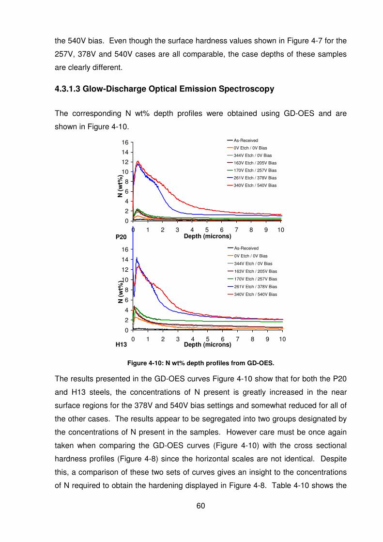
60
the 540V bias. Even though the surface hardness values shown in Figure 4-7 for the
257V, 378V and 540V cases are all comparable, the case depths of these samples
are clearly different.
4.3.1.3 Glow-Discharge Optical Emission Spectroscopy
The corresponding N wt% depth profiles were obtained using GD-OES and are
shown in Figure 4-10.
P20
0
2
4
6
8
10
12
14
16
0 1 2 3 4 5 6 7 8 9 10Depth (microns)
N (
wt%
)
As-Received
0V Etch / 0V Bias
344V Etch / 0V Bias
163V Etch / 205V Bias
170V Etch / 257V Bias
261V Etch / 378V Bias
340V Etch / 540V Bias
H13
0
2
4
6
8
10
12
14
16
0 1 2 3 4 5 6 7 8 9 10Depth (microns)
N (
wt%
)
As-Received
0V Etch / 0V Bias
344V Etch / 0V Bias
163V Etch / 205V Bias
170V Etch / 257V Bias
261V Etch / 378V Bias
340V Etch / 540V Bias
Figure 4-10: N wt% depth profiles from GD-OES.
The results presented in the GD-OES curves Figure 4-10 show that for both the P20
and H13 steels, the concentrations of N present is greatly increased in the near
surface regions for the 378V and 540V bias settings and somewhat reduced for all of
the other cases. The results appear to be segregated into two groups designated by
the concentrations of N present in the samples. However care must be once again
taken when comparing the GD-OES curves (Figure 4-10) with the cross sectional
hardness profiles (Figure 4-8) since the horizontal scales are not identical. Despite
this, a comparison of these two sets of curves gives an insight to the concentrations
of N required to obtain the hardening displayed in Figure 4-8. Table 4-10 shows the

61
peak N wt% concentration and the N wt% concentration at a depth of 10µm. The
GD-OES analysis reveals information about the compound layer thickness and the
subsurface N concentration which gives rise to the hardening response.
Peak N wt% N wt% at 10µm Peak N wt% N wt% at 10µm Treatment / Material P20 H13
0V Etch, 0V Bias 1.1 0.2 2.6 0.3 344V Etch, 0V Bias 1.8 0.3 3.8 0.5
163V Etch, 205V Bias 2.2 0.2 4.8 0.6 170V Etch, 257V Bias 2.5 0.5 4.6 1.7 261V Etch, 378V Bias 11.6 1.1 14.4 2.2 340V Etch, 540V Bias 12.1 1.4 12.9 2.1
Table 4-10: Tabulated values from Figure 4-10 showing the concentration of N in wt% at the peak and at 10µm.
4.3.2 Summary
As discussed in section 2.8, Georges [6] asserted that the samples to be treated in a
similar commercial ASPN system can be maintained at a floating potential, or are
subjected to a small negative bias of 100 to 200V [48]. The results of this section
show that in general, a higher bias produces to an improved hardening response.
The response is material dependent with the maximum case depth achieved for
biases of at least 378V for P20 and 540V for H13. In the latter case, a higher bias
may result in a further increase in case depth. It is clear that for the ASPN system
and steels investigated, more than a few hundred volts bias is required to achieve a
good hardness response. The results of this section also showed that surface
hardness alone is not sufficient to determine the effects on the hardening response of
varying the bias. In the case of H13, the surface hardness was similar for biases
between 257V to 540V, however the cross sectional hardness revealed significant
differences in the case depths of these samples. The apparent discrepancy between
the results in this thesis and other work in which good nitriding responses were
obtained with floating bias (see section 2.8), may be explained by the large size of
the commercial ASPN system employed in this work. Most other studies have been
performed on laboratory size systems where the sample to active screen separation
is much smaller. The effect of varying the sample to active screen distance is
investigated further in Chapter 6.

62
4.4 Effect of gas mixture on nitriding response
The following study focuses on the effects of varying the ratio of N2/H2 gas mixture on
the nitriding response while the other treatment conditions remained fixed. The aim
was to investigate the effect of gas mixture during ASPN on the nitriding response of
P20.
4.4.1 Experiment
The nitriding response was determined from surface and cross sectional hardness
tests. N depth profiles were obtained using GD-OES. In addition, X-Ray diffraction
(XRD) was used to identify the nitride phases present as a function of N2 gas mixture
concentration. Four separate treatments were carried out, each at a specific gas
mixture, with a fixed bias setting of 30% as outlined in Table 4-11 and Table 4-12.
Treatment Parameter
Step 1 (Heat up)
Step 2 (Etch)
Step 3 (Nitride)
Step Time (min) ~180 30 360 Pressure (mbar) 0.75 1.5 2.0
Gas Mixture
100% H2 50% Ar, 50% H2
90% N2, 10% H2 50% N2, 50% H2
25% N2, 75% H2
5% N2, 95% H2 Bias OFF ON ON
Temp (°C) 520 520 520
Table 4-11: Table showing the range of treatment parameters. Step 1 was a heat up from room temperature. At the end of step 3 the system is back filled with N2 to approximately 0.9 bar and
fan cooled.

63
Etch Step Nitride Step
Treatment Iscreen (A)
Vscreen (V)
Iwork (A)
Vwork (V)
Iscreen (A)
Vscreen (V)
Iwork (A)
Vwork (V)
90% N2, 10% H2 60 339 9.36 347 73 376 9.37 355 50% N2, 50% H2 61 351 9 345 42 406 9.04 458 25% N2, 75% H2 77.1 370.4 9.08 339.4 62.6 452.5 9.27 539.5 5% N2, 95% H2 66 350 8.98 328.1 55 445.7 9.07 694.6
Table 4-12: Indicated values for the current and voltage for each treatment. Note that the bias
for the workload (Vwork) is the RMS value.
4.4.2 Results and Discussion
4.4.2.1 Effect of gas mixture on the bias voltage
The bias voltage sustained on the base plate and the components to be treated is
determined by the plasma conditions surrounding the base plate inside the ASPN
system. The plasma resistance therefore determines the bias voltage sustained on
the base plate and the components to be treated. The bias power supply voltage is
treatment dependant i.e. influenced by gas composition and pressure. The relation
between the gas mixture and the RMS bias voltage for the ASPN system is shown in
Figure 4-11.
An increase in the N2 gas mixture concentration while keeping the bias setting control
fixed and the overall chamber pressure fixed yields a reduction in the bias. Therefore
the bias and the N2 gas mixture concentration are coupled variables. This decrease
in bias voltage for a constant current can be explained by a reduction in plasma
resistance as the ratio of N2 to H2 decreases. The reduction in plasma resistance is
explained by an increase in charge carriers as the concentration of N2 increases.
However, the ionisation potential (IP) for N2 and H2 are 15.5808eV and 15.4259eV
respectively [76] and therefore the IP differences do not account for the observed
trend for the bias (Figure 4-11). Another probable explanation is that with an
increase in the N2 concentration, the secondary electron generation increases as the
proportion of the more massive N2 ions hitting the workload increases. This would
result in more charge carriers and a reduction in the plasma resistance.

64
0
100
200
300
400
500
600
700
800
0 20 40 60 80 100
Bia
s (
V)
30% Bias
20% Bias
10% Bias
7% Bias
Figure 4-11: The effect that N2 gas mixture concentration had on the RMS bias voltage. Shown is the voltage variation for variable N2 gas mixture concentration in % for a fixed pressure of 2
mbar and fixed temperature of 520ºC.
4.4.2.2 Surface Hardness
The average surface hardness response for the four P20 substrates treated using the
different gas mixtures is shown in Figure 4-12.
0
200
400
600
800
1000
1200
90 50 25 5 As-Received
Su
rfa
ce
Ha
rdn
es
s (
HV
/0.1
)
Figure 4-12: Effect of treatment gas composition on the surface hardness of the four P20
samples (Average values shown). 95% CI for the population mean shown (Confidence Level α = 0.05 and Degrees of Freedom = 4 for t test).
N2 Gas Mixture Concentration (%)
N2 Gas Mixture Concentration (%)

65
The as-received hardness value for P20 was measured at 349 HV. Using the 95%
CI for the estimation of the population mean of surface hardness, it was found that
each of the treated samples had the same hardness of approximately 800 HV and
therefore no one gas mixture treatment was more effective than any other in
improving surface hardness.
4.4.2.3 Cross Sectional Hardness Profiles
The cross sectional hardness profiles for a P20 substrate nitrided at various N2/H2
gas mixtures are shown in Figure 4-13. Four different experiments were undertaken
where the treatment gas mixture was varied from 5% N2 to 90% N2 as detailed in
Table 4-12.
0
200
400
600
800
1000
0 50 100 150 200Depth (microns)
HV
(0.1
)
90%
50%
25%
5%
As-Received
P20
Figure 4-13: Hardness depth profiles for each P20 sample indicated by the N2 gas mixture
concentration in %. The solid line indicates the as-received hardness value of the substrate.
The depth profiles are similar for the N2 gas mixture concentrations investigated
within the range 90% - 25% N2. The case depths were found to be 115, 110, 100
and 90 (µm) for the 90% N2, 50% N2, 25% N2, 5% N2 mixes respectively. These
results show that the 5% N2 gas mixture treatment had a reduced case depth.

66
4.4.2.4 Glow-Discharge Optical Emission Spectroscopy
The corresponding N wt% depth profiles were obtained using GD-OES and are
shown in Figure 4-14.
0
2
4
6
8
10
12
14
16
18
0 1 2 3 4 5 6 7 8 9 10Depth (microns)
N (
wt%
)
90%50%25%5%As-Received
P20
Figure 4-14: N depth profiles (wt%) as measured from GD-OES. The N concentration (wt%) varies considerably in the near surface region, however at larger depths regardless of the
ASPN gas composition the curves coincide. The insert shows the concentration over 80µm for 50% N2 sample.
In all cases the N concentration is at its highest level in the near surface region (0.5 -
1µm) after which all four curves reduce to ~1.5 wt% at 10µm. The concentration of N
at and beyond 10µm was found to be the similar regardless of the gas mixture and
slowly reduce over the next 80µm as shown in the insert in Figure 4-14. The N
concentration depth profiles are similar for the other gas mixtures, although the 25%
N2 curve shows the N concentration profile falling more rapidly below 2µm. The
hardness profiles in Figure 4-13 show a hardness increase of 400-450 points from
the as-received hardness in the region 10 - 50µm. This hardness response
correlates with a 1 - 2 wt% N concentration present in the diffusion zone, as is
evident from the GD-OES profiles shown in Figure 4-14. It is evident that the 5% N2
curve shows the highest concentration of N just below the surface which reduces
rapidly near the surface. This was further investigated by plotting the O depth
profiles (Figure 4-15). The results show that the O concentration at the near surface
for the 5% N2 treatment is of the order of 60 wt% O and reduces to less than 2 wt%
0
2
4
0 20 40 60 80Depth (microns)
N (
wt%
)
50%

67
over the first 2µm. This suggests that the formation of an oxynitride at the surface
reduces both the compound layer thickness and the subsurface depth of hardening
(see Figure 4-13).
0
10
20
30
40
50
60
70
80
0 0.5 1 1.5 2Depth (microns)
O (
wt%
)
90%
50%
25%
5%
P20
Figure 4-15: O depth profiles (wt%) as measured from GD-OES over the first 2µm for the four treatment conditions.
4.4.2.5 Microstructure
Cross sectional scanning electron microscopy (XSEM) images Figure 4-16 were
obtained by sectioning and polishing the samples before a final etch with 2% nital
solution.
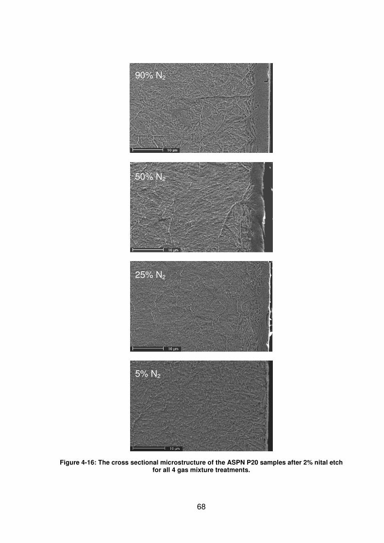
68
Figure 4-16: The cross sectional microstructure of the ASPN P20 samples after 2% nital etch for all 4 gas mixture treatments.
90% N2
50% N2
25% N2
5% N2

69
Figure 4-16 is a series of four cross sectional optical micrographs of P20 samples
showing the change in microstructure as the N2 gas mixture concentration
decreases. The compound layer thickness was measured to be 4.9, 4.5, 3.3, and
0.7µm for 90%, 50%, 25% and 5% N2 treatment conditions respectively. The
compound layer reduces in thickness as the N2 gas mixture concentration decreases,
this is consistent with previous findings [16], that is, the compound layer thickness
reduces as the nitriding potential decreases. The interface between the compound
layer and the diffusion zone is characterised by needle like precipitation (Fe4N) as
discussed previously by Seybolt [30]. Note that the entire region below the
compound layer in these figures is the diffusion zone. The diffusion zone itself is
characterized by precipitation in both the grain boundaries and within the grains. It is
evident that these precipitates reduce in size as the nitriding potential reduces.

70
4.4.2.6 Compound layer tests
The SEM micrographs showing typical Rockwell hardness indentations on each of
the nitrided surfaces treated at the different N2 gas mixtures are shown in Figure
4-17.
Figure 4-17: Optical micrographs of the Rockwell indents for all four nitrided samples.
90% N2
50% N2
25% N2
5% N2

71
In all cases surface cracks are apparent. The cracks are both concentric and radial
with the indent, and there is no obvious correlation between the compound layer
thickness, as observed in Figure 4-16, and the severity or number of cracks (Figure
4-17). The results show that all of the compound layers are well adhered and no
delamination or spalling was observed.
4.4.2.7 X-Ray Diffraction
Examination of the XRD profiles in Figure 4-18, reveals that the majority of the
information is collected from a sample depth of up to 5µm since there are no distinct
α-Fe peaks appearing in the 90% and 50% N2 profiles of the XRD spectrum (Figure
4-18). With the increase of N2 gas mixture concentration, the compound layer
thickness increases (Figure 4-16), thus the α-Fe peak height from XRD (Figure 4-18)
decreases accordingly. In addition, Figure 4-18 shows an increase in both ε (Fe2-3N)
and γ' (Fe4N) iron nitride phases until a N2 gas mixture concentration of 25%, beyond
which the ε (Fe2-3N) iron nitride phase begins to dominate the iron nitride component
of the spectrum. This result is similar to that of Bell et al. [17], where they employed
a cross sectional analysis using X-Ray diffraction. It was shown that the iron nitride
ratio ε (Fe2-3N) to γ' (Fe4N) decreased as a function of depth until only γ' (Fe4N) could
be observed.

72
Figure 4-18: XRD spectrum of the 4 ASPN P20 samples, including the XRD profile for as-received P20. Note the strong α-Fe peaks in the 5% N2 curve. Note that each spectrum is
plotted with a 200 point linear offset for clarity.
The XRD patterns in Figure 4-18 show that a combination of iron nitrides γ' (Fe4N)
and ε (Fe2-3N) phases are present for each of the samples. The N2 lean gas mixture
with 5% N2 is enough to form both γ' (Fe4N) and ε (Fe2-3N) iron nitrides, however the
contribution from ε (Fe2-3N) is less than γ' (Fe4N). Also in the 5% N2 case the α-Fe
substrate peaks still appear which suggests that only a thin compound layer formed
which is consistent with the metallographic examination, see Figure 4-16. It is
evident that the XRD patterns for the samples treated at 50% N2 and 90% N2 are
almost identical. The GD-OES results show a peak concentration of around 17 wt%
N for the sample treated at 5% N2. According to the Fe-N equilibrium phase diagram
(Figure 2-1) this concentration of N should be enough to form the ζ (Fe2N) phase
[12]. There is no evidence in the XRD patterns for the presence of this phase. This
may be due to the ζ (Fe2N) phase not being significant enough in the analysed
volume to produce discernable peaks in the XRD patterns.

73
4.4.2.8 Model for the compound layer thickness and case depth
A model was developed that relates the nitride case depth to the N2 gas mixture
concentration and bias experimental conditions. It was shown [77, 78] that the
nitriding case depth d can be related to the nitriding conditions and to the properties
of the steel by:
( )RXNDtd /2=
where N is the surface nitrogen concentration (at%), X is the original nitriding alloy
element concentration (at%), R is the ratio of N to alloy element in the nitride phase,
D is the diffusion coefficient of N in ferrite (m2/sec) and t is the time of nitriding (sec).
This equation was originally developed for the internal oxidisation of alloys by Jack et
al. [16, 74, 75].
The concentration of dissolved N into the topmost surface layer will in the first
instance be determined by the available N2 in the gas mixture, i.e. the available N. In
addition, the bias will cause N ions to be accelerated to the sample surface,
increasing the surface concentration to levels (far) above gas equilibrium values.
The surface concentration N should therefore be proportional to both the N2 available
in the gas mixture and bias as expressed by
Bias2VNN ×∝
For constant temperature T and time t values, the variables (D, t, R and X) in
Equation (1) are constant. Therefore the nitriding depth or case depth becomes:
biasVNDepthCase ×∝2
Figure 4-19a shows the case depth plotted against biasVN ×2
. It is clearly a straight
line, which is consistent with our hypothesis that the N surface concentration is a
function of the N2 gas mixture concentration and the bias.
With respect to our present experimental findings, a plot of compound layer thickness
(dcl) against case depth thickness (dcd) is shown in Figure 4-19b. These results
indicate that there is a relationship between the compound layer thickness and the
case depth. In particular, the gradient of the straight line shows that in this example
the case depth is about 27 times thicker than the compound layer.

74
80
90
100
110
120
130
50 100 150 200√(N2*Vbias)
Cas
e D
ep
th (
mic
ron
)
0
1
2
3
4
5
6
80 90 100 110 120 130Case Depth (micron)
Co
mp
ou
nd
lay
er
thic
kn
es
s
(mic
ron
)
Figure 4-19: a) The case depth plotted as a function of the N2 gas mixture concentration and the bias. b) Measurements of compound layer thickness as a function of the case depth for
each of the samples analysed.
We now calculate the ratio dcd/dcl, using Equation (1) to compare with the measured
value of 27. The nitriding time is constant (tcd = tcl), the sample is uniformly
distributed with the same nitriding components (Xcd = Xcl) and we take interface
concentrations of N for the compound layer and case depth to be within the same
order of magnitude. This yields,
cl
cd
cl
cd
cl
cd
R
R
D
D
d
d≈
where the two diffusion coefficients, Dcd and Dcl indicate diffusion in the case and
compound layer respectively. The value for Dcl can be split up into at least 2
components. That is Dcl-γ’, Dcl-ε, the diffusion co-efficient for the part of the compound
layer due to the γ' (Fe4N) phase and the part of the compound layer due to the ε (Fe2-
3N) phase. These values were calculated previously to be, [28, 29].
a)
b)

75
Dcl-γ’ ≈ 6x10-14 m2/sec at 520ºC
Dcl-ε ≈ 1.6x10⁻¹⁴ m2/sec at 520ºC
The value for Dcd was calculated previously to be ~4.2E-12 m2/sec at 520ºC [13, 79],
for the α-Fe lattice.
The ratio of the two diffusion coefficients is 100/DDclcd
≈ . The R term in Equation (1)
is obtained from the GD-OES results in Figure 4-14 and is found to be: cdcl RR 6≈ .
Using these values, dcd/dcl is calculated from Equation (4) to be ~24. This result
compares well with the value of dcd/dcl 27≈ as measured from the slope of the
straight line fit shown in Figure 4-19b.
The deviation from the linear behaviour in Figure 4-19b in the 5% N2 case is probably
due to increased sputtering resulting from the higher bias of this sample (Figure
4-11). The fitted line in Figure 4-19b intersects the zero compound layer axes for
case depth value of ~80µm. This suggests that there can be a substantial case
depth while not forming a compound layer.
4.4.3 Summary
The nitriding response of four P20 steel substrates prepared using different gas
mixtures in the ASPN system was investigated. The increase in surface hardness
was similar for all of the gas mixtures, even for a low N2 gas mixture concentration of
5%. Rockwell indents revealed that the compound layer in all cases is well adhered.
Cross sectional hardness analysis showed the case depths were significant for all of
the gas mixture cases. XRD showed the development of the iron nitride phases as
the N2 gas mixture concentration increased. In all gas mixture cases both iron nitride
phases γ' (Fe4N) and ε (Fe2-3N) could be observed.

76
Regardless of the gas mixture used a compound layer and a diffusion zone was
produced and the thickness of these layers varied as the square root of the product
of the N2 gas mixture concentration and the bias. Using the equation developed by
Jack et al. [16, 74, 75], it is shown that both the compound layer thickness and the
case depth can be mathematically related to each other. These results show that for
a given nitriding time and temperature the case depth depends on the N availability
at the sample surface and the bias.
4.5 Conclusion
The major finding of this chapter is that without a bias during the nitriding step there
is effectively little or no nitriding response in terms of case depth in the steels
investigated. A pre-nitride plasma etch did not improve the hardness response
except for H13, where an etch was found to be beneficial. Further investigations
showed that the level of bias required depends on the steel. In the case of P20, a
bias of 378V was sufficient to produce a case depth of approximately 90µm
compared to H13 which required a bias of 540V to achieve approximately the same
case depth.
Another finding of this chapter was that a decrease in the N2 gas mixture
concentration for a fixed bias setting yields an increase in the voltage sustained on
the base plate. However, this increase in base plate bias voltage for the changing
gas mixtures investigated did not produce any significant change in either the surface
or cross sectional hardness levels except for the 5% case where a limited surface N
availability may have been responsible. Also, a model was presented demonstrating
that in this commercial ASPN system the effective nitriding depth and the thickness
of the compound layer are determined by the bias voltage and the N2 gas mixture
concentration.

77
Chapter Five
5 The role of the Active Screen in ASPN
In Chapter 4, the effect of the key treatment parameters in ASPN on the nitriding
response of selected steels was investigated. The aims of this chapter were to
determine whether the nitriding response depends on the active screen material and
to test the hypothesis that a mechanism of mass transfer of N in the commercial
ASPN system is one of sputtering material from the active screen and deposition
onto the samples. This was achieved by carrying out experiments using two different
active screens made from two different materials: mild steel (MS) and a high alloy
(HA) steel which contained 20 wt% Cr and 36 wt% Ni. The presence of high
concentrations of these elements on the substrate surfaces can then be used to
determine whether mass transfer had occurred, and what effect this has, if any, on
the nitriding response.
5.1 The effect of active screen material on the nitriding response
5.1.1 Experiment
A full factorial experiment considering 3 factors at 2 levels, i.e. 23 treatments (Table
5-1) was carried out to investigate the effects of selected treatment parameters; bias,
etching and active screen material, on the nitriding response of P20, H13, 4140 and
1020 steels. One sample from each steel was placed on the base plate and the
automated treatment cycle as set out in Table 5-3 started. The treatment parameters
are detailed in Table 5-2. Base pressure prior to step 1 (Table 5-3) was 4 x 10⁻²
mbar.

78
Treatment
A (Bias)
B (Etch)
C (Active Screen
material) 1: Bias on, Etch on, MS +1 +1 -1 2: Bias on, Etch off, MS +1 -1 -1 3: Bias off, Etch on, MS -1 +1 -1 4: Bias off, Etch off, MS -1 -1 -1 5: Bias on, Etch on, HA +1 +1 +1 6: Bias on, Etch off, HA +1 -1 +1 7: Bias off, Etch on, HA -1 +1 +1 8: Bias off, Etch off, HA -1 -1 +1
Table 5-1: Experimental Design, for the 3 factors at 2 levels. The active screen material is either MS (-1) or HA (+1). Treatment 1 is therefore Bias On, Etch On and MS screen.
Etch Step Nitride Step
Treatment Iscreen (A)
Vscreen (V)
Iwork (A)
Vwork (V)
Iscreen (A)
Vscreen (V)
Iwork (A)
Vwork (V)
1: Bias on, Etch on, MS 61 351 9 345 42 406 9 458 2: Bias on, Etch off, MS - - - - 72 413 9 407 3: Bias off, Etch on, MS 69 355 9 334 101 457 - - 4: Bias off, Etch off, MS - - - - 102 440 - - 5: Bias on, Etch on, HA 67 341 9 309 64 423 9 429 6: Bias on, Etch off, HA - - - - 68 410 9 423 7: Bias off, Etch on, HA 81 350 9 308 100 443 - - 8: Bias off, Etch off, HA - - - - 101 440 - -
Table 5-2: Indicated values for the current and voltages for each treatment. Note that the bias
for the workload (Vwork) is the RMS value.
Treatment Parameter
Step 1 (Heat up)
Step 2 (Etch)
Step 3 (Nitride)
Step Time (min) ~180 30 360 Pressure (mbar) 0.75 1.5 2.0
Gas Mixture 100% H2 50% Ar, 50% H2 50% N2, 50% H2 Bias OFF OFF or ON OFF or ON
Temp (°C) 520 520 520
Table 5-3: Table showing the range of treatment parameters. Step 1 was a heat up from room temperature. At the end of step 3 the system is back filled with N2 to approximately 0.9 bar and
fan cooled.
5.1.2 Results and Discussion
In this section, samples were analysed using the same basic techniques as those
used in Chapter 4.

79
5.1.2.1 Surface Hardness
The surface hardness results are presented in Figure 5-1 using the 95% CI for the
estimation of the population mean for both the MS and HA active screens. The
results show that the surface hardness in all steels is significantly increased above
that of the as-received substrate hardness when the bias is on for treatments using
both active screen materials, MS and HA. The effect of etching is less significant
although in the case of H13 it appears to be beneficial. This is in agreement with the
results presented in Chapter 4.
0
200
400
600
800
1000
1200
1400
P20 H13 4140 1020Material
Su
rface H
ard
ness
(H
V/0
.1)
Etch + Bias (MS) Etch + Bias (HA) Bias Only (MS)Bias Only (HA) Etch Only (MS) Etch Only (HA)No Etch No Bias (MS) No Etch No Bias (HA) As-Received
Figure 5-1: Effect of treatment conditions on surface hardness for all steels and experimental treatments. 95% CI for the mean treatment hardness are shown (α = 0.05 and d = 4 for t-test).
The effects of the main factors A and B (Table 5-1) were obtained from the surface
hardness values (Figure 5-1) using ANOM. The ANOM for both the MS and HA
active screens is shown in Figure 5-2 for the deviation of the overall material surface
hardness from the material treatment mean to enable all materials to appear on the
same plot.

80
-300
-200
-100
0
100
200
300
P20 A
-1
P20 A
+1
H13
A-1
H13
A+1
4140
A-1
4140
A+1
1020
A-1
1020
A+1
P20 B
-1
P20
B+1
H13
B-1
H13
B+1
4140
B-1
4140
B+1
1020
B-1
1020
B+1
Material and Factor Level
Ha
rdn
ess
Dev
iati
on
(H
V/0
.1)
Effect of the EtchEffect of the Bias
MS and HA Screen
Figure 5-2: ANOM for both MS (—) and HA (—) active screens showing the deviation from the
overall treatment mean of surface hardness by material for the main factors A and B. For both MS and HA active screens, only factor A (Bias) is significant for all the materials. Only H13
shows an effect to factor B (Etch).
The ANOM showing the effect of the main factor C (Table 5-1) is shown on the left
hand side of Figure 5-3, while the right hand side shows the interaction between the
main factors A and B (Table 5-1) with the effects of both the MS and HA active
screens averaged out.

81
-400
-200
0
200
400
600
P20 C
-1
P20 C
+1
H13
C-1
H13
C+1
4140
C-1
4140
C+1
1020
C-1
1020
C+1
P20
A-1
'
P20
A+1
'
H13
A-1
'
H13
A+1
'
4140
A-1
'
4140
A+1
'
1020
A-1
'
Material and Factor Level
Ha
rdn
es
s D
ev
iati
on
(H
V/0
.1)
Effect of the Screen material Interaction between the Bias and Etch
Figure 5-3: ANOM for factor C (active screen material) (—) and the interaction between factor
A (Bias) and factor B (Etch) (—), showing the deviation from the overall treatment mean of
surface hardness by material for the main factor C and the interaction between the main factors AB (Bias and Etch).
Under the ASPN conditions investigated, it can be concluded from the ANOM for
both the MS and HA active screens that all materials have a significant surface
hardness response to bias. Only H13 shows a significant surface hardness response
to the etch. Additionally H13 had a significant interaction between the etch and the
bias. The results suggest that the surface hardness response of all the steels
investigated is independent of the composition of the active screen material.
5.1.2.2 Cross Sectional Hardness Profiles
Hardness depth profiles (Figure 5-4), measured on polished sectioned samples,
show the hardening response by material. The four material hardness profile plots
using the MS active screen for the four combinations of etch and bias are plotted in
Chapter 4 of this thesis (Figure 4-4). The plots shown in Figure 5-4 compare the
nitriding response for bias on/etch on and no bias/no etch conditions for both MS and
HA active screens.

82
0
200
400
600
800
1000
1200
0 50 100 150 200Depth (microns)
HV
(0.1
)
Etch + Bias (MS)
Etch + Bias (HA)
No Bias No Etch (MS)
No Bias No Etch (HA)
As-Received
P20 - MS and HA
0
200
400
600
800
1000
1200
0 50 100 150 200Depth (microns)
HV
(0.1
)
Etch + Bias (MS)
Etch + Bias (HA)
No Bias No Etch (MS)
No Bias No Etch (HA)
As-Received
H13 - MS and HA
0
200
400
600
800
1000
1200
0 50 100 150 200Depth (microns)
HV
(0.1
)
Etch + Bias (MS)
Etch + Bias (HA)
No Bias No Etch (MS)
No Bias No Etch (HA)
As-Received
4140 - MS and HA
0
200
400
600
800
1000
1200
0 50 100 150 200Depth (microns)
HV
(0.1
)
Etch + Bias (MS)
Etch + Bias (HA)
No Bias No Etch (MS)
No Bias No Etch (HA)
As-Received
1020 - MS and HA Figure 5-4: Hardness depth profiles shown for P20, H13, 4140 and 1020 steels across 2
treatments and both active screen materials.

83
It is evident from Figure 5-4 that the hardness profiles fall broadly into two
populations. The first population is one showing a classical hardening response for
bias on/etch on for both MS and HA active screens. The trend for the alloy steels is
one of increasing hardness but decreasing depth of hardness with increasing alloy
content (Table 4-4). As observed by Seybolt [30], the presence of strong alloy nitride
forming elements such as Cr in a material during a nitriding treatment caused an
appreciable hardening response. The results in Figure 5-4 can be interpreted on the
basis of increased trapping of N in the higher alloy steels leading to greater
precipitation of fine alloy nitrides in H13 while in P20, 4140 and 1020, less trapping of
N leads to greater depths of diffusion by interstitial N but sufficient super-saturation of
N in solid solution to give rise to a compound layer.
A comparison between the hardness profiles for the MS and HA treatments can be
made by considering the uncertainties shown in Figure 4-3. The results shown in
Figure 5-4 indicate that there is a significant difference between the bias on and etch
on treatments of the H13 steel and to a lesser extent of P20 for the two active screen
materials MS and HA. The increase in hardness case depth for the MS active screen
treatment above the HA active screen treatment is also shown by comparing the
values presented in Table 4-5 with Table 5-4. It is evident that the largest increase in
case depth when comparing the effects of the active screen occurs for H13. The
increase in case depth for MS active screen in comparison to HA active screen can
also be seen to a lesser extent for the 4140 steel and less again for the P20 and
1020 steels (Figure 5-4). Despite the surface hardness of the samples showing no
response to the active screen material (Figure 5-3), the case depths for the samples
treated with the HA active screen (Figure 5-4) are less than those observed for the
MS treatments. One interpretation of this could be the effect of active screen
material deposition, if any, on the surface of the samples. If active screen material
deposition occurs during the nitriding treatment as Li et al [48] suggest, then the
effect on the nitriding response may be more significant with the HA active screen
compared to that of the MS active screen due to the active screen material
composition. The deposition of strong alloy nitride forming elements such as Cr (20
wt% for the HA active screen) on the sample surface could restrict the diffusion of N
into the sample material. The strong presence of Cr and Ni at the sample surface
would have a large affinity for N, thereby forming stable alloy nitrides and limiting the
N diffusion into the sample bulk. Moreover, if such a process occurred, the net effect

84
on the nitriding response would be dissimilar across sample material since, as
discussed previously, the sample materials with higher alloy element concentrations
results in greater trapping of N in the sample material. The second population
(Figure 5-4) shows a low hardening response in all materials for the no bias/no etch
condition.
Treatment / Material P20 H13 4140 1020 1: Bias on, Etch on 105 60 110 N/A 2: Bias off, Etch off N/A N/A N/A N/A
Table 5-4: Case depth values in µm for the two treatments across four steels using the HA
active screen.
5.1.2.3 Glow-Discharge Optical Emission Spectroscopy
The corresponding N wt% depth profiles for treatments for the MS and HA active
screens obtained from GD-OES for the bias on/etch on and no bias/no etch
conditions are shown in Figure 5-5.

85
02468
10121416
0 5 10 15 20Depth (microns)
N (
wt
%)
Etch + Bias (MS)Etch + Bias (HA)No Bias No Etch (MS)No Bias No Etch (HA)As-Received
P20 - MS and HA
0
2
4
6
8
10
12
14
16
0 5 10 15 20Depth (microns)
N (
wt
%)
Etch + Bias (MS)Etch + Bias (HA)No Bias No Etch (MS)No Bias No Etch (HA)As-Received
H13 - MS and HA
02468
10121416
0 5 10 15 20Depth (microns)
N (
wt
%)
Etch + Bias (MS)Etch + Bias (HA)No Bias No Etch (MS)No Bias No Etch (HA)As-Received
4140 - MS and HA
0
2
4
6
8
10
12
14
16
0 5 10 15 20Depth (microns)
N (
wt
%)
Etch + Bias (MS)Etch + Bias (HA)No Bias No Etch (MS)No Bias No Etch (HA)As-Received
1020 - MS and HA
Figure 5-5: N wt% depth profiles from GD-OES. Note the overall similarities of N content between treatments with the two active screen materials for the two treatments shown.

86
It is important to consider that the plots shown in Figure 5-5 are representative of the
first 20µm into the sample surface, where the plots shown in Figure 5-4 represent the
hardness profiles over 200µm. As discussed in the background of this thesis, as the
concentration of interstitial N in the α-Fe matrix increases beyond 0.1 wt% N, the
precipitation of γ’- Fe4N iron nitride phase begins to occur. The precipitation of γ’-
Fe4N is responsible for a large portion of the hardening response. This effect can be
observed by considering the H13 steel. At a depth of 10µm for the H13 GD-OES
profile (Figure 5-5), the N concentration is around 2 wt%. This concentration of N in
the α-Fe matrix is only sufficient to precipitate γ’- Fe4N with interstitial N in solid
solution. When considering the H13 hardness profile (Figure 5-4), the hardness at
around 10µm is comparable to the maximum hardness obtained by the nitriding
treatment. The N concentration at the tail end of the GD-OES profiles (Figure 5-5) is
therefore responsible for producing large case depths, where as discussed
previously. This concentration as a function of depth is dependent on the presence
of strong alloy nitride forming elements within the steels. In comparison, the GD-
OES profiles for the bias and etch off conditions show limited uptake of N at the
sample surface, which supports the cross sectional hardness profiles (Figure 5-4).
However there was a small uptake of N in the H13 case over the first few microns
which correlates well with the cross sectional hardness profiles for the sample (Figure
5-4).
5.1.3 Summary
The comparison of both the cross sectional hardness profiles and the GD-OES
results for treatments using MS and HA active screens showed that there was a
difference in both the hardness profiles and the N concentration as a function of
depth into the substrates. The hardness profiles appear to be hindered by
treatments using the HA active screen, which is supported by the GD-OES results. If
material transfer occurs from the active screen to the sample surface, then the
deposition of strong alloy nitride forming elements on the sample surface could be
responsible for reducing the N uptake into the substrate surface. However it should
be noted that the sputtering rates for the MS and HA active screens may differ due to
differences in the concentration of stable oxides present on the active screens.

87
5.1.4 Mass transfer from the Active Screen
To establish whether mass transfer from the active screen to the samples occurred in
the ASPN system, two polished P20 samples were analysed after one was nitrided
using the MS active screen while the other was nitrided using the HA active screen.
The results of the GD-OES analysis are shown in Figure 5-6. It is evident that Ni is
present for several hundred nm on the surface of the sample treated using the HA
active screen while little or no Ni is present on the nitrided sample treated with the
MS active screen. This demonstrates unequivocally that material was transferred
from the active screen to the parts being treated in the commercial ASPN system.
However the significance of this result was further investigated in order to understand
its effect, if any, on the nitriding response of samples in an ASPN system.
0
0.2
0.4
0.6
0.8
1
1.2
0 2 4 6 8 10
Depth (microns)
Ni (w
t%)
P20 Using MS Screen
P20 Using HA Screen
P20 As-Received
P20
Figure 5-6: Compositional depth profiles for Ni using GD-OES on the surface of P20 samples
after nitriding with a MS active screen (—) and with a HA active screen (—). For comparison,
a GD-OES analysis of the surface of an as-received P20 (—) is shown.

88
5.1.5 The nature of material transferred
In this section a Field Emission Scanning Electron Microscope (FESEM) analysis
was used to investigate material transfer from the active screen. A simple factorial
experiment was designed in which hardened and tempered H13 (HH13) and Si
samples were treated using the MS and HA active screens. Si substrates were
selected in order to limit the interaction between any material deposited and the
substrate. The two types of active screens employed in this investigation were the
same as those used in the previous section, that is MS and HA.
5.1.5.1 Experimental
N type phosphorus doped Si samples were prepared by dicing wafers into 10mm
squares. Each sample was given a standard cleaning treatment, dried and placed on
the base plate. The treatment parameters for the different nitriding cycles
investigated are shown in Table 5-5. Steps 2 and 3 (Table 5-5) refer to the nitriding
cycles for the Si samples subjected to ASPN treatments using MS and HA steel
active screens, respectively. Step 4 refers to a nitriding cycle carried out on HH13.
The bias was set at a constant current of ~9A.
Treatment
Parameter
Step 1
(Heat up)
Step 2
(Nitride for Si)
Step 3
(Nitride for Si)
Step 4
(Nitride for HH13)
Step Time (min) ~180 360 360 540
Pressure (mbar) 0.75 2.0 2.0 2.0
Gas Mixture 100% H2 25% N2, 75% H2 50% N2, 50% H2 50% N2, 50% H2
Bias OFF OFF or ON OFF or ON ON
Temp (°C) 520 520 520 520
Screen Material MS/HA MS HA MS
Table 5-5: Table showing the range of treatment parameters. At the end of the respective nitride cycles the system was back filled with N2 to approximately 0.9 bar and fan cooled.

89
5.1.6 Results and Discussion
5.1.6.1 Active Screen Material Deposition: MS Screen
Figure 5-7 is a FESEM micrograph of the surface of a Si substrate after completion of
the heating step only using the MS active screen (i.e. Step 1 only). It clearly reveals
the presence of a high number density (~460 particles/µm2) of mostly equi-axed nano
particles ranging in size from 20-90nm. Some nano particles appear more chain like
with a length to width ratio of over 2:1. The nano particles appear to be separated by
a fine open boundary measuring just less than 10nm in width. This is a significant
result, since at this point in the ASPN treatment, the only component subject to a bias
voltage was the active screen. This result confirms that mass transfer is taking place
from the MS active screen, resulting in the deposition or formation of nano particles
on the Si substrate.
Figure 5-7: Secondary electron image of a Si substrate showing the nano particle distribution
after heating only with the MS active screen.
Figure 5-8a is a FESEM micrograph of a Si surface after an ASPN treatment in which
no etch or bias was applied during a 6 hour nitriding cycle. The effect on the nano
particle distribution is significant in that there now appears to a bimodal distribution of
particles. The larger equi-axed particles are around 100nm in diameter with a
number density of ~100 particles/µm2. A few of the larger particles again show a
length to width ratio of around 2:1. The larger particles are widely spaced and within
this inter-particle space is a collection of nano particles about 10-20nm in diameter.
The number density of the larger particles has decreased significantly which
suggests that particle growth had taken place by particle coalescence and/or Ostwald
Ripening [80] during the extended heating period in the N2/H2 environment. The

90
nano particles in the inter-particle space may well have resulted from further
deposition during the nitriding cycle. Figure 5-8b is a FESEM micrograph of a Si
surface after an ASPN treatment in which an etch and bias was applied during the
nitriding cycle. It is evident that the number density (~330 particles/µm2) has only
slightly decreased from that of the heat only cycle (See Figure 5-7, ~460
particles/µm2). This suggests that the effect of etch and bias had been to impede
particle growth.
Figure 5-8: Secondary electron images of Si substrates after ASPN treatment using a MS active screen showing a) the nano particle distribution with no bias/no etch and b) the nano particle
distribution with bias and etch.
Figure 5-9 shows the corresponding XTEM images for the Si substrates shown in
Figure 5-8. The surface of the Si substrate shown in Figure 5-9a (no bias/no etch)
appears unmodified by the treatment with little or no modification of the
microstructure and the native oxide remains intact. Deposited on top of the Si
surface are particles that vary in size up to ~100nm in width. This result compares
well with the FESEM images presented in Figure 5-8a. The XTEM image of the
sample prepared using both etch and bias (Figure 5-9b) is quite different to the no
a)
b)

91
bias/no etch case. It can be seen from the XTEM image that the nano particles are
deposited at a range of depths and are of varying sizes. However care must be
exercised in evaluating the size of these deposited nano particles since the cross
section may not necessarily pass through the largest section of nano particles. Of
particular interest is the surface modification of the Si substrate seen in Figure 5-9b.
In addition, the Si surface is rough, presumably due to ion bombardment that
occurred during either/both of the etch or bias stages of the nitriding treatment. In
addition, there are clear line defects observed beneath the Si surface (for example,
see arrow in Figure 5-9b). These defects are characteristic of the type described by
Jeng et al. [81], where they were attributed to energetic H ion bombardment. To
investigate these defects further, XTEM images for the Si substrates are shown in
Figure 5-10 for the intermediate conditions of etch only (Figure 5-10a) and bias only
(Figure 5-10b). In the case of etch only (Figure 5-10a), in addition to the particle
deposition, there is clear evidence for surface roughening caused by energetic Ar ion
bombardment during the etch. This result supports the proposition that an etch may
be beneficial in some cases where a boundary layer (e.g. surface oxide) may need to
be removed to increase the nitriding response. Both samples also show defects
beneath the Si surface. Since H2 was used in both the etch only and bias only
stages, the H ions are responsible for inducing defects in the Si substrate. The
corresponding indexed diffraction pattern for Figure 5-10a is shown in Figure 5-11.
The red circle in Figure 5-11 indicates the super-lattice effect due to the {111} platelet
defects. These platelets give rise to diffraction spots along the <111> directions,
close together due to their large separation in the sample. These platelet defects
have been described by others [81, 82] and are caused by energetic H ion
bombardment. Muto et al. [82] suggest that defects aggregate on the {111} planes
and form platelet defects upon annealing.

92
Figure 5-9: Cross sectional TEM micrographs for the conditions: a) MS active screen, no
bias/no etch, b) MS active screen, bias and etch (the arrow points to defects in the Si substrate).
Figure 5-10: Cross sectional TEM micrographs for the conditions: a) MS active screen, etch only, b) MS active screen, bias only.
a)
b) Si Substrate
Si Substrate
a)
b)
Si Substrate
Si Substrate

93
The depth of the modified region, as calculated using SRIM 2006 [83] for a Si
substrate as a function of the bias power, is shown in Table 5-6. The modified area
under investigation is indicated by the arrow in Figure 5-9b. The ion energies used in
the SRIM calculations correspond to the RMS value and the peak value of the pulses
for a bias setting of 30% (Table 3-2). The results of these simulations are tabulated
in Table 5-6 and reveal the maximum implantation depth of penetration of the various
ionic species. The ionic species chosen are those that are expected to be generated
in the plasma around the samples using the gas mixtures (N2/H2) and (Ar/H2) during
the nitriding and etch treatments.
It can be seen from the results in Table 5-6 that there is a correlation between the
maximum depth of penetration of 1250eV H+ ions (131nm) and the depth of the H
induced defects seen in the TEM images of Figure 5-9b and Figure 5-10 which occur
to depths of between 100 and 150nm. This confirms the assumption made earlier
that, since H2 was used in both the etch only and bias only stages, H ions are
responsible for the defects observed in the Si substrate. The result also shows that
the high voltage pulses associated with the bias power supply signature (see section
3.4) affect the energies of the bombarding ion species. This is not surprising since
the pulses associated with the bias power supply are not dissimilar to the pulsed
biases used in a technique known as Plasma Immersion Ion Implantation (PIII) [84-
86]. PIII is a materials surface modification technique that can be used to enhance
surface properties, such as, wear resistance, surface hardness and surface resistivity
[84-86]. PIII involves applying a pulsed bias to the sample to be treated and is
normally applied to conducting and semiconducting materials.
Ion Energy (eV) H2+ N2
+ Ar+ H+ N+
500 42.5 11.5 7 77 18 1250 88 20.5 12 131 32.5
Table 5-6: Simulated values for the maximum depth in nm of penetration of various ions in a Si
substrate, given in nm from SRIM 2006 [83].

94
Figure 5-11: The corresponding diffraction pattern with a [011] zone axis for the TEM image
shown in Figure 5-10a. Note that the red circle indicates the super-lattice effect.
In order to explicitly show the nature of the deposited nano particles on the Si
surface, EFTEM (Figure 5-12) was undertaken in search of Fe on both Si substrates
shown in Figure 5-9. The results shown in Figure 5-12 unambiguously confirm that
the deposited nano particles are Fe rich and supports the interpretation of the results
presented earlier in this section.

95
Figure 5-12: Cross sectional EFTEM micrographs for the conditions: a) MS active screen, no bias/no etch, Fe elemental map, b) MS active screen, bias and etch, Fe elemental map.
5.1.6.2 Active Screen Material Deposition: HA Screen
The experimental conditions used to generate Figure 5-8a and Figure 5-8b were
repeated using the HA active screen. The objective was to unambiguously identify
active screen material deposited on the Si surface. Figure 5-13a is a FESEM
micrograph of a Si surface after an ASPN treatment with no etch or bias applied in
the nitriding cycle. It is evident that there is a much finer nano particle distribution
compared to the MS active screen case (Figure 5-8a), with a number density of ~940
particles/µm2 and a particle size ranging from 20-50nm. The fine distribution of nano
particles can be attributed to the increase in strong alloy nitride forming elements
associated with the HA steel active screen. Figure 5-13b is a FESEM micrograph of
a Si sample after an ASPN treatment in which an etch and bias was applied during
the nitriding cycle. The effect of the treatment in this case was to distinctly change
the morphology of the nano particle distribution. The nano particles appear to have
grown in a chain-like or dendritic mode generating an open three dimensional
Si Substrate
a)
b)
Si Substrate

96
network structure. This growth mode can be attributed to the active screen material
composition since both etch and bias was applied in this treatment.
Figure 5-13: Secondary electron images of Si substrates after ASPN treatment using a HA steel
active screen showing a) the nano particle distribution with no bias/no etch and b) the nano-particle distribution with bias and etch.
The corresponding XTEM images for the results of Figure 5-13 are shown in Figure
5-14. There is only limited surface modification for the no bias/no etch treatment
shown in Figure 5-14a, which is similar to that seen in Figure 5-9a. Figure 5-14
reveals that there is some triangular particle growth beneath the Si surface. These
features were not visible in the XTEM images of samples treated using the MS active
screen which suggests that they result from the Cr or Ni in the HA active screen.
Surface roughening had also occurred for the etch and bias treatment (Figure 5-14b)
as observed previously for the MS case (Figure 5-9b). There also appears to be a
fine nano particle deposition on the Si surface shown in Figure 5-14a which is in
agreement with the FESEM image shown in Figure 5-13a. In addition, there appears
a)
b)

97
to be a more continuous layer on the Si surface shown in Figure 5-14b which is in
agreement with the FESEM result presented in Figure 5-13b.
Figure 5-14: Cross sectional TEM micrographs for the conditions: a) HA active screen, no bias/no etch, b) HA active screen, bias and etch.
EFTEM was undertaken (Figure 5-15) to determine the nature of the particles that
appear to have grown into the surface of the Si in Figure 5-14. The elemental map
reveals that the triangular particles are Ni based (Figure 5-15a). The growth of Ni
particles in the surface of Si substrates to form NiSi has been investigated previously
[87-89]. The formation of NiSi is not well understood, however, it is reported [89] that
NiSi formation is dependent on the Si surface conditions and the thickness of the Ni
film. This result verifies that material transfer from the active screen had occurred to
the sample surface since the active screen was the only source of Ni during these
experiments. Also shown is a Fe elemental map (Figure 5-15b) confirming a Fe layer
on the sample surface.
a)
b)
Si Substrate
Si Substrate

98
Figure 5-15: Cross sectional EFTEM micrographs for the condition: etch and bias, a) Ni elemental map and b) Fe elemental map.
5.1.7 The effect of mass transfer on the nitriding response
The last section established unambiguously that there was mass transfer from both
the MS and HA active screens to the workload surfaces during ASPN treatment.
Indeed much of the transfer appears to take place in the heating stage which is not
surprising given that the highest power is applied to the active screen during the heat
up phase of the treatment. Additionally it was established that the bias can
significantly influence the morphology of nano particles deposited on Si surfaces
when applied during the nitriding phase. The challenge remaining was to establish
whether or not the deposition of nano particles was beneficial to the nitriding
response. It should be noted, as discussed in section 2.8, that one of the nitriding
mechanisms in ASPN was attributed to the sputtering of active screen material and
its deposition as iron nitride onto the workload [48, 62]. This issue was addressed by
comparing the response of HH13 steel to ASPN treatments in which one set of steel
samples was treated normally by placement on the open base plate while the other
set was placed under a shield (in effect, a steel plate approximately 300mm in
diameter placed some 300mm above the HH13 samples (Figure 5-16)). The latter
was done in an attempt to shield the HH13 steel sample from a line of sight mass
transfer from the active screen. Both substrates had the same bias voltage.
Si Substrate
a) b)
Si Substrate

99
Figure 5-16: Experimental set up for the shielding and exposed ASPN experiments. Note the
shield was supported by three metal rods and the MS active screen was used in this treatment.
A comparison of the nitriding response for HH13 in terms of the subsurface hardness
profiles for the above two conditions treated within the same load is shown in Figure
5-17a. Figure 5-17b shows the surface hardness results based on five
measurements for the shielded and exposed samples. It is evident that although the
surface hardness of the two steel samples is much the same, the case depths are
different. More specifically, the case depth for the shielded samples is ~110µm and
~80µm for the exposed sample. This result is further supported by micro-structural
examination of the two steel samples, see Figure 5-18a and Figure 5-18b. The
shielded sample had a compound layer thickness of ~4.5µm while the exposed
sample showed no compound layer within the resolution of the metallographic
examination. This result confirms that the deposited particles reduce the nitriding
potential since both samples were subject to the same bias voltage. Therefore the
shielded sample had a much higher nitriding potential due to its treatment outside the
line of sight of material transfer from the active screen.

100
0
200
400
600
800
1000
1200
0 50 100 150 200 250Depth (microns)
HV
(0.
1)
Shielded HH13
Exposed HH13
(a)
0
200
400
600
800
1000
1200
1400
Shielded HH13 Exposed HH13
Su
rfa
ce
Ha
rdn
es
s (
HV
/0.1
)
(b)
Figure 5-17: a) Cross sectional hardness profiles for HH13 treated for 540 minutes – shielded and exposed, b) Surface hardness values for HH13 - shielded and exposed.

101
Figure 5-18: Optical Micrographs of metallographic cross-sections of HH13 samples showing
a) the compound layer on the shielded sample, b) no resolvable compound layer on the exposed sample and c) FESEM of a shielded Si sample after heating only showing a very fine
distribution of nano particles.
These results appear to call into question the suggestion by Li et al. [48] that material
transfer from the active screen is the primary mechanism of N mass transfer in ASPN
given that when one shields a steel sample from direct line of sight of the active
screen the case depth is increased. Such a conclusion is tempered by the result
shown in Figure 5-18c. This is a Si sample treated as per the sample in Figure 5-7,
that is heated only, but shielded in a similar fashion to the shielded HH13 sample. It
is evident that there are only a few nano particles in the size range 20-40nm but
there appears to be many nano particles in a size range less than 10nm. The origin
of these nano particles may be from the shield itself or from non-direct line of sight
material transfer from the active screen. Clearly, there is a lower density of deposited
nano particles in Figure 5-18c compared to Figure 5-7.
a) b)
c)

102
5.1.8 Isolating the Active Screen
The previous section demonstrated that material transfer from the active screen to
the sample surface did not appear to enhance the hardening response of the HH13
steel investigated. In this section the aim was to investigate if a nitriding response
could be achieved by totally isolating the active screen from the nitriding cycle. This
was achieved by switching the power supply off to both the active screen and the
base plate and using a temperature controlled filament heater inside an insulating
ceramic case to supply heat for the experiment (Figure 5-19). The heater assembly,
shown in Figure 5-20 was placed on the base plate inside the ASPN chamber. An
HH13 sample was then placed on top of the heater which was capable of sustaining
a bias voltage and was biased via an appropriate connection. For safety reasons,
the applied bias voltage was supplied by an independently regulated DC bias power
supply and not the inbuilt bias supply in the ASPN system. The electrical
connections made to the external power supply were via electrical feed throughs.
The treatment conditions of this experiment are detailed in Table 5-7.
Treatment Parameter
Step 1 (Heat up)
Step 2 (Nitride 400V DC)
Step 2 (Nitride 550V DC)
Step Time (min) ~45 360 360 Pressure (mbar) 1.5 3.5 2.0
Gas Mixture 100% H2 25% N2, 75% H2 25% N2, 75% H2 Sample Bias OFF ON ON Temp (°C) 520 520 520
Table 5-7: The treatment conditions for the two nitriding experiments using the independent
heating device for both bias settings of 400V DC and 550V DC.
Figure 5-19: A schematic showing the experimental apparatus employed in this study. Note that both the active screen and bias power supplies were switched off during the experiment.

103
Figure 5-20: The mini heater assembly and a polished HH13 sample sitting on the base pate in
the ASPN system.
The corresponding cross sectional hardness profiles for the two HH13 samples
nitrided at 400V DC and 550V DC are shown in Figure 5-21. Also shown for
comparison purposes, is the hardness profile of a HH13 sample treated on the base
plate in the ASPN system with the active screen. The treatment conditions used
were, 25% N2, 75% H2 gas mixture at 520ºC for 360 minutes using a bias of 514V
RMS/1200V Peak. It can be seen that there is a significant surface hardness
response for all three samples. However, the three depth profiles are significantly
different from one another over the first 30µm and the case depth values are given in
Table 5-8.
As expected, the sample treated using the 550V DC bias showed an increased
response in comparison to the sample treated with the 400V DC bias. In addition,
the sample treated using the 550V DC bias produced a significant hardening
response in the absence of the active screen. However, the sample treated on the
base plate with the active screen and a bias of 514V RMS/1200V Peak, produced the
largest case depth (Table 5-8). This is not unreasonable since the last section
showed that the peak voltages associated with the bias effect the energy of the
incident ions, giving rise to the increased nitriding response in comparison to the
sample treated with the 550V DC bias.

104
0
200
400
600
800
1000
1200
1400
0 50 100 150 200Depth (microns)
HV
(0
.1)
Mini Heater (400V DC)
Mini Heater (550V DC)
Base (514V RMS/1200V Peak)
As-Received
HH13
Figure 5-21: The cross sectional hardness profiles for the HH13 samples treated with the independent heating device at 400V DC and 550V DC bias voltages. For comparison, the plot of
Base HH13 sample treated on the base plate at 514V RMS/1200V Peak.
Treatment / Material HH13 Mini Heater (400V DC) 5 Mini Heater (550V DC) 25
Base (514V RMS/1200V Peak) 40
Table 5-8: Table of case depths in µm for the two HH13 samples treated with the independent heating device at 400V DC and 550V DC bias voltages. Also given is the case depth value for
the Base HH13 sample treated on the base plate at 514V RMS/1200V Peak.
The corresponding N wt% depth profiles from GD-OES for the two treatments using
the independent heating device are shown in Figure 5-22. Also shown is the profile
of the HH13 sample treated on the base plate in the ASPN system as mentioned
earlier in this section. The GD-OES results presented confirmed the limited
hardening response for the HH13 sample treated with a 400V DC bias, with the
maximum N concentration around 2 wt% at the surface which reduces to almost zero
within 20µm. However, the surface N concentration of 2 wt% is sufficient to
precipitate γ’- Fe4N with interstitial N in solid solution which gives rise to the high
surface hardness. In addition, the N concentrations shown for the samples treated
with the 550V DC bias and the sample treated on the base plate at 514V RMS/1200V
Peak bias supports the hardness profiles shown in Figure 5-21. In the case of the
HH13 sample treated with a 550V DC bias, the surface N concentration is of the
order of 4 wt% and reduces to almost zero within 40µm. The HH13 sample treated
on the base plate shows the largest N concentration compared to that of the other
two samples.
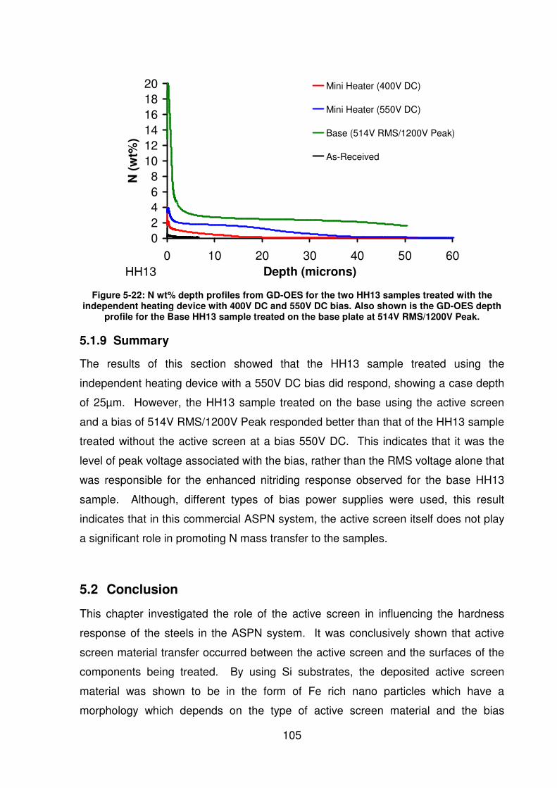
105
02468
101214161820
0 10 20 30 40 50 60Depth (microns)
N (
wt%
)
Mini Heater (400V DC)
Mini Heater (550V DC)
Base (514V RMS/1200V Peak)
As-Received
HH13
Figure 5-22: N wt% depth profiles from GD-OES for the two HH13 samples treated with the independent heating device with 400V DC and 550V DC bias. Also shown is the GD-OES depth
profile for the Base HH13 sample treated on the base plate at 514V RMS/1200V Peak.
5.1.9 Summary
The results of this section showed that the HH13 sample treated using the
independent heating device with a 550V DC bias did respond, showing a case depth
of 25µm. However, the HH13 sample treated on the base using the active screen
and a bias of 514V RMS/1200V Peak responded better than that of the HH13 sample
treated without the active screen at a bias 550V DC. This indicates that it was the
level of peak voltage associated with the bias, rather than the RMS voltage alone that
was responsible for the enhanced nitriding response observed for the base HH13
sample. Although, different types of bias power supplies were used, this result
indicates that in this commercial ASPN system, the active screen itself does not play
a significant role in promoting N mass transfer to the samples.
5.2 Conclusion
This chapter investigated the role of the active screen in influencing the hardness
response of the steels in the ASPN system. It was conclusively shown that active
screen material transfer occurred between the active screen and the surfaces of the
components being treated. By using Si substrates, the deposited active screen
material was shown to be in the form of Fe rich nano particles which have a
morphology which depends on the type of active screen material and the bias

106
conditions. Although active screen material mass transfer was shown to occur, there
was no evidence that this process plays any significant positive role in the nitriding
process. Indeed, this chapter presented evidence that the deposition of active
screen material may inhibit the nitriding process. Furthermore, by using Si
substrates, evidence was produced that shows substrates on the base plate undergo
ion bombardment effects due to the application of the bias. These implantation
effects are consistent with the output waveform of the bias power supply which
contains high voltage pulses up to 1200V at the 30% bias value employed. The
results also indicate that the peak voltages associated with the bias power supply
play a role in accelerating ions to the sample surface.
The role of the active screen in the nitriding process was investigated further by
comparing the response of HH13 nitrided conventionally on the base plate with
samples biased and heated independently. The nitriding response of a HH13 sample
treated on the base plate with the active screen showed an increased nitriding
response in comparison to a HH13 treated with the independent heater and power
supply with the absence of the active screen. However, the level of peak voltage
associated with the bias in the base sample treatment is more likely to be responsible
for the increased nitriding response which suggests that the active screen in the
ASPN system does not play a significant role in enhancing the nitriding response.
The peak voltage of the pulsed power supply is more likely to be the critical factor in
determining the nitriding response.

107
Chapter Six
6 Further ASPN Investigations
The evidence presented in this thesis so far all points to substrate bias as the most
important factor which determines the nitriding response of steels in the commercial
ASPN system. The question that this raises is why these findings are apparently
different to the work of other researchers in which nitriding was successfully
performed with no substrate bias (see section 2.8). The main difference between the
commercial system used here, and the laboratory based systems used in most other
studies is size and in particular the distance between the active screen and the
components to be treated. This chapter investigates the effect of the physical
location of substrates as a function of height in the ASPN chamber and therefore the
distance between the components and the active screen. This chapter also presents
results from experiments which compared the nitriding response of substrates
surrounded by a mini active screen to those placed on an insulating support and
others biased in the conventional way outlined in earlier chapters.
6.1 The nitriding response as a function of height in the chamber
The experiments for this study involved placing the experimental apparatus (Figure
6-1) directly on the base plate within the ASPN chamber such that the samples
remained at an equivalent potential of the base plate (Figure 6-2). The steel chosen
for this investigation was P20, and one sample was placed on each of the positions
on the experimental equipment as seen in Figure 6-1 and Figure 6-2. The treatment
times for this section of the experiments were 360 minutes.
The heights of the samples above the base plate for this experiment are detailed in
Table 6-1. Base pressure prior to nitriding treatment was 4 x 10⁻² mbar and the gas
mixture was selected to be 25% N2, 75% H2. The indicated values for the current
and voltages of this experiment are detailed in Table 6-2.

108
Position on experimental apparatus – #1 at the
Bottom
Base plate experiment
Height (mm)
Distance from sample
to screen (mm)
1 32 1508 2 50 1490 3 70 1470 4 88 1452 5 107 1433 6 182 1358 7 331 1209
Table 6-1: Experimental values for the investigation of the nitriding response as a function of height in the ASPN chamber.
Etch Step Nitride Step
Treatment Iscreen (A)
Vscreen (V)
Iwork (A)
Vwork (V)
Iscreen (A)
Vscreen (V)
Iwork (A)
Vwork (V)
Base Plate 60 426 11.6 488 62 445 9 552 Table 6-2: Indicated values for the current and voltages during the etch and bias stages. Note
that the bias for the workload (Vwork) is the RMS value.
Figure 6-1: Experimental apparatus employed for this experiment.

109
Figure 6-2: A picture of the experimental apparatus employed in this study, shown here placed
directly on the ASPN base plate.
6.1.1 Results and Discussion
6.1.1.1 Surface Hardness
The results in Figure 6-3 were plotted using the 95% CI for the estimation of the
population mean. The surface hardness of the samples treated show a good surface
hardness response with no systematic trend with distance above the base plate.
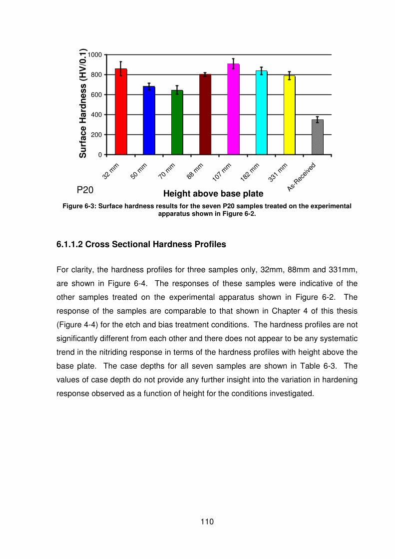
110
0
200
400
600
800
1000
32 m
m
50 m
m
70 m
m
88 m
m
107
mm
182
mm
331
mm
As-Rec
eived
Height above base plate
Su
rface H
ard
ness (
HV
/0.1
)
P20
Figure 6-3: Surface hardness results for the seven P20 samples treated on the experimental apparatus shown in Figure 6-2.
6.1.1.2 Cross Sectional Hardness Profiles
For clarity, the hardness profiles for three samples only, 32mm, 88mm and 331mm,
are shown in Figure 6-4. The responses of these samples were indicative of the
other samples treated on the experimental apparatus shown in Figure 6-2. The
response of the samples are comparable to that shown in Chapter 4 of this thesis
(Figure 4-4) for the etch and bias treatment conditions. The hardness profiles are not
significantly different from each other and there does not appear to be any systematic
trend in the nitriding response in terms of the hardness profiles with height above the
base plate. The case depths for all seven samples are shown in Table 6-3. The
values of case depth do not provide any further insight into the variation in hardening
response observed as a function of height for the conditions investigated.

111
0
200
400
600
800
1000
0 50 100 150 200Depth (microns)
HV
(0.1
)
32mm
88mm
331mm
As-Received
P20
Figure 6-4: Hardness profiles for three P20 samples treated on the experimental apparatus shown in Figure 6-2. The results are shown for the 32mm, 88mm and 331mm conditions only
for clarity.
Height above base plate (mm)
Case Depth in µm
32 100 50 80 70 80 88 105
107 90 182 105 331 110
Table 6-3: Table of case depths in µm for the seven P20 samples treated on the experimental
apparatus shown in Figure 6-2.
6.1.1.3 Glow-Discharge Optical Emission Spectroscopy
The corresponding N wt% depth profiles for the treatment are shown in Figure 6-5.
In order to present the GD-OES results in a tabulated manner, the GD-OES results
are shown in Table 6-4 for the depth at which the N wt% concentration has dropped
to 6 wt% and the N wt% at a depth of 5µm. The value of 6 wt% was chosen based
on an interpretation of the Fe-N equilibrium phase diagram (Figure 2-1), where to a
first approximation, at N concentrations higher than 6 wt% the formation of a dual
phase FeN occurs, giving rise to a compound layer formation. Using this
interpretation, the compound layer thickness can be estimated to be the depth at

112
which the N concentration drops below 6 wt% from the sample surface, however this
does not take into account other alloying elements present in the sample materials
utilised throughout this study. The depth of 5µm was chosen to give an estimate for
the concentration of N in the diffusion region.
Height above base plate
0
2
4
6
8
10
12
14
16
18
0 1 2 3 4 5
Depth (microns)
N (
wt%
)
32 mm50 mm70 mm88 mm107 mm182 mm331 mmAs-Received
P20 Figure 6-5: GD-OES profiles for P20 samples as a function of height in the ASPN system. Note
the vertical scale.
Height above base
plate (mm) Depth (µm)
when N wt% = 6%
N wt% at 5µm depth
32 1.4 1.4 50 0.9 1.3 70 0.1 1.2 88 1.6 1.3
107 1.6 1.3 182 1.3 1.2 331 1.7 1.5
Table 6-4: Tabulated results for Figure 6-5, detailing the depth at which the N wt% has reduced to 6 wt% and the N wt% concentration at a depth of 5µm in the sample surface.
The results of this section have demonstrated that the compound layer thickness
varies approximately between 0.1µm and 1.7µm which was inferred from the
tabulated figures in Table 6-4. This would tend to suggest that the nitriding potential
of the 50mm and 70mm samples were reduced in comparison to the other samples,
however, there does not appear to be any systematic trend with height variation
above the base plate. The subsurface concentration of N in the samples tabulated in
Table 6-4 at a depth of 5µm and beyond is responsible for the hardening response
seen in the hardness profiles (Figure 6-4).

113
6.1.2 Summary
In this section, the nitriding response of samples as a function of height above the
base plate was investigated. No systematic trend was found for the sample to active
screen separation distances from 120 to 150cm. This result suggests that the
nitriding response of a large commercial component in the ASPN system with an
applied bias is expected to uniform over its height up to 150cm.
6.2 Proximity Experiments
The experiments presented in this section were undertaken in an attempt to increase
the proximity of the plasma sheath that surrounds the active screen and the surface
of the samples. This study is essentially a reproduction of the study published by Li
et al. [48], where the nearest physical distance between the active screen and the
sample surface was of the order of 12mm. The experiments were designed to
compare the nitriding response of samples placed in three different environments as
shown in Figure 6-6. One set of samples were placed directly on the base plate,
another set were placed directly on an electrically insulating post and the final set
were placed on another electrically insulating post and then surrounded by a mini
active screen made from mild steel (MS). Throughout this section, these three
environments are referred to as base, insulator and mini screen respectively.
6.2.1 Experimental set up
The three sets of samples were treated within the same nitriding cycle. The sample
material employed in this section of this study was P20 and H13 in the hardened and
tempered condition (HH13).
The mini screen that surrounded the samples atop the insulating post can be seen in
the right hand side of Figure 6-7 while the insulating post can be seen on the left
hand side of this figure. During the nitriding treatment, the nearest distance of the
mini screen to the sample surface was 12mm in accordance to model that of the
experiments of Li et al. [48]. The open area fraction of the mini screen was 47%.
The power was supplied to the mini screen by direct connection to the base plate.
The samples that were placed underneath the mini screen had no applied bias and
were therefore at a floating potential. Base pressure prior to nitriding treatment was
4 x 10⁻² mbar and the gas mixture was selected to be 25% N2, 75% H2, the treatment
time was 360 minutes. The indicated values for the current and voltages of these

114
experiments are detailed in Table 6-5, where the etch step was not included in the
treatment due to complexity of the experimental arrangement.
Figure 6-6: A schematic of the location of the samples inside the ASPN chamber, a) residing atop the insulating post and surrounded by the mini screen, b) Atop the insulator. c) Sitting
directly on the base.
Figure 6-7: A picture of the insulating post and the mini screen made from MS employed in this
study.
Etch Step Nitride Step Treatment Iscreen
(A) Vscreen
(V) Iwork (A)
Vwork (V)
Iscreen (A)
Vscreen (V)
Iwork (A)
Vwork (V)
For a), b) and c) - - - - 56 448 9 514 Table 6-5: Indicated values for the currents and voltages for the nitriding treatment for all three sets of samples a), b) and c) shown in Figure 6-6. Note that the bias for the workload (Vwork) is
the RMS value.

115
6.2.2 Results and Discussion
6.2.2.1 Surface Hardness
The surface hardness results shown in Figure 6-8 were plotted using the 95% CI for
the estimation of the population mean. The results demonstrate that the surface
hardness is, in all three cases of mini screen, insulator and base, greater than that of
the as-received condition. The samples that were treated with the mini screen
displayed a significant surface hardness response, whereas the base samples
showed a further improved response, particularly in the HH13 case. The insulator
samples also responded, producing a significant surface hardness response. This
initially appears to be contradictory to the results presented earlier (Chapter 4) in this
thesis (Figure 4-1) which showed that a bias was essential to obtaining a good
nitriding response. However the point must be made here that the surface hardness
results alone are not a good indicator of the overall nitriding response and so cross
sectional hardness tests were performed.
0
200
400
600
800
1000
1200
1400
P20 HH13Material
Su
rfa
ce
Ha
rdn
es
s (
HV
/0.1
)
Mini Screen Insulator Base As-Received
Figure 6-8: Surface hardness results for the two steels and the three experimental conditions.
6.2.2.2 Cross Sectional Hardness Profiles
The cross sectional hardness profiles presented in Figure 6-9 give a more thorough
examination of the nitriding response. The case depths (Table 6-6) are greatest for
the mini screen treatments for both materials. In addition, this result has shown that

116
the proximity of the active screen to the substrates is an important parameter in
enhancing the nitriding response when no bias is applied to the substrates. The case
depths (Table 6-6) for the base samples are reduced in comparison to the mini
screen sample case depths. The insulator samples exhibit a poor nitriding response
in terms of the case depth, where they are further reduced in comparison to the base
samples. Interestingly, the case depths of the mini screen samples are significantly
increased in comparison to the insulator samples. This change in response can only
be attributed to the effects of the mini screen since all other experimental conditions
remained the same. The results presented in this section are in agreement with
those presented by Li et al. [48], where a electrically floating EN40B steel was
treated using a mini active screen with a nearest distance of 12mm to the sample
surface. Upon examination of the cross sectional hardness profile presented by Li et
al. [48] for the EN40B sample material, the case depth, using the same methods as
employed in this study was calculated to be ~70µm, which is similar to the case
depth measured of 65µm for the HH13 material of similar elemental composition.
Treatment / Material P20 HH13
Mini Screen 110 65 Insulator N/A 15
Base 90 40
Table 6-6: Case depth values in µm for all three treatments and two steels.

117
0
200
400
600
800
1000
1200
1400
0 50 100 150 200Depth (microns)
HV
(0
.1)
Mini ScreenInsulatorBaseAs-Received
P20
0
200
400
600
800
1000
1200
1400
0 50 100 150 200Depth (microns)
HV
(0.1
)
Mini ScreenInsulatorBaseAs-Received
HH13
Figure 6-9: Cross sectional hardness profiles, shown for the three sets of experiments and two steels.
6.2.2.3 Glow-Discharge Optical Emission Spectroscopy
The corresponding N wt% depth profiles for the three sets of samples are shown in
Figure 6-10. It can be seen, towards the 30µm end of the plots that for all of the
sample materials, the concentration of N in the sample is increased for the mini
screen and base experiments in comparison to the insulator treatments. Considering
both materials, the concentration of N at a depth of 25µm for the mini screen samples
is of the same order of magnitude as that displayed for the base samples (Table 6-7).
This result demonstrates that surrounding the samples with a mini screen can
facilitate the uptake of N into the sample surface without the need for a substrate
bias. This uptake of N without a bias is responsible for the case depths (Table 6-6)
observed for the mini screen samples.

118
Peak N wt% N wt% at 10µm N wt% at 25µm Treatment / Material P20
Mini Screen 14.5 1.1 1.1 Insulator 7.2 0.3 0.2
Base 17.1 1.1 0.9 HH13
Mini Screen 10.6 2.3 2.2 Insulator 6.8 0.5 0.3
Base 19.9 2.7 2.4
Table 6-7: Tabulated values from Figure 6-10 showing the concentration of N in wt% at the peak, 10µm and 25µm.
02468
101214161820
0 5 10 15 20 25 30Depth (microns)
N (
wt%
)
Mini Screen
Insulator
Base
As-Received
P20
02468
101214161820
0 5 10 15 20 25 30Depth (microns)
N (
wt%
)
Mini Screen
Insulator
Base
As-Received
HH13
Figure 6-10: GD-OES N wt% profiles, shown to 30µm with inserts shown to 5µm.
02468
101214161820
0 1 2 3 4 5Depth (microns)
N (
wt%
)
P20
02468
101214161820
0 1 2 3 4 5Depth (microns)
N (
wt%
)
HH13

119
6.2.3 Summary
It was shown that a sample treated on an insulating post could be successfully
nitrided by surrounding it with a mini screen. The response, in terms of case depth,
of P20 and HH13 samples treated with the biased mini screen were found to be
better than those biased on the base plate in the way described in section 4.1.
These findings indicate that the proximity of the mini screen to the samples is a
critical factor which determines whether it is possible to nitride without a bias in an
ASPN system.
6.3 Separation of the mini screen and the samples
A series of experiments were designed to explore the effects of the sample to screen
separation in an attempt to further understand the mechanism that facilitates
nitriding. It should be noted that the work presented in this section was undertaken
with a treatment time of 540 minutes, whereas in previous sections it was 360
minutes. The steels chosen for this investigation in this section of the experiments
were P20, H13 and HH13.
6.3.1 Experimental set up
The arrangement of the samples within this commercial ASPN chamber can be seen
in Figure 6-11. The insulating post and mini screen that was used in previous
sections of this chapter was also used in this section. The mini screen was raised up
on electrically conducting pads to vary the sample to screen distance. The five
distances chosen for this study were 12mm, 20mm, 28mm, 50mm and 70mm where
the power supplied to the mini screen was from the direct connection to the base
plate. Base pressure prior to the nitriding treatment was 4 x 10⁻² mbar and the gas
mixture was selected to be 25% N2, 75% H2 for all treatments. The indicated values
for the current and voltages of these experiments are detailed in Table 6-8 where the
etch step was not included in the treatment due to complexity of the experimental
arrangement. The treatment conditions for the treatments are detailed in Table 6-9.

120
Figure 6-11: A schematic of the location of the substrates inside this commercial ASPN
chamber. The distance from the sample surface to the mini screen was varied from 12mm, 20mm, 28mm, 50mm and 70mm, by means of a vertical displacement.
Etch Step Nitride Step Treatment Iscreen
(A) Vscreen
(V) Iwork (A)
Vwork (V)
Iscreen (A)
Vscreen (V)
Iwork (A)
Vwork (V)
12mm - - - - 71 454 9 488 20mm - - - - 84 466 9 495 28mm - - - - 68 449 9 506 50mm - - - - 82 460 9 493 70mm - - - - 80 462 9 480
Table 6-8: Indicated values for the currents and voltages for the nitriding treatment for all five sets of samples, 12mm, 20mm, 28mm, 50mm and 70mm. Note that the bias for the workload
(Vwork) is the RMS value.
Treatment Parameter
Step 1 (Heat up)
Step 2 (Nitride)
Step Time (min) ~180 540 Pressure (mbar) 1 2
Gas Mixture 100% H2 25% N2, 75% H2 Sample Bias OFF ON Temp (°C) 520 520
Table 6-9: The treatment conditions for the nitriding treatment for all five sets of samples, 12mm, 20mm, 28mm, 50mm and 70mm.
6.3.2 Results and Discussion
6.3.2.1 Surface Hardness
The surface hardness results for the three steels, P20, H13 and HH13 at five
different separations, 12mm, 20mm, 28mm, 50mm and 70mm from the mini screen
can be seen in Figure 6-12. It can be seen that there is no clear trend for the surface
hardness with the separation from the mini screen over the investigated conditions.

121
0
200
400
600
800
1000
1200
P20 H13 HH13Material
Su
rfac
e H
ard
nes
s (
HV
/0.1
)
12mm 20mm 28mm 50mm 70mm As-Received
Figure 6-12: The surface hardness response, shown across materials. The distance from the sample surface to the mini screen is shown in the graph key.
6.3.2.2 Cross Sectional Hardness Profiles
The cross sectional hardness profiles for the three steels, P20, H13 and HH13 at five
different separations, 12mm, 20mm, 28mm, 50mm and 70mm from the mini screen
are shown in Figure 6-13. The hardness profiles indicate that the nitriding response
is not significantly different for 12mm, 20mm or 28mm sample to mini screen
separations across all of the sample materials. However, the nitriding response for
the 50mm and 70mm experiments are significantly greater than the response from
the 12mm, 20mm and 28mm experiments. The case depths for the three sample
materials across the five treatments are shown in Table 6-10. The case depth values
for the 50 and 70mm experiments of P20 indicate a similar response (115µm),
whereas, for H13 and HH13 there exists significant differences between the two
experiments.

122
0
200
400
600
800
1000
1200
0 50 100 150 200Depth (microns)
HV
(0
.1)
12mm20mm28mm50mm70mmAs-Received
P20
0
200
400
600
800
1000
1200
0 50 100 150 200Depth (microns)
HV
(0
.1)
12mm20mm28mm50mm70mmAs-Received
H13
0
200
400
600
800
1000
1200
0 50 100 150 200Depth (microns)
HV
(0.1
)
12mm20mm28mm50mm70mmAs-Received
HH13
Figure 6-13: The cross sectional hardness profiles for P20, H13 and HH13 steels treated for
540 minutes in the commercial ASPN system surrounded by a mini screen at varying separations.

123
Sample to mini screen separation / Material
P20 H13 HH13
12mm 75 40 35 20mm 20 55 40 28mm 10 45 50 50mm 115 70 60 70mm 115 85 75
Table 6-10: Case Depth values in µm for all three steels and five sample to mini screen separations.
6.3.2.3 Glow-Discharge Optical Emission Spectroscopy
The GD-OES profiles for the three sets of samples treated under the mini screen at
varying separations can be seen in Figure 6-14. The results from GD-OES confirm
the results seen in the cross sectional hardness profiles (Figure 6-13). It is observed
that the 12mm, 20mm and 28mm profiles are similar to those presented in Figure
6-10, where for P20, the N concentration in the sample is of the order of 1 wt%. For
the H13 and HH13 steels, there is a depth where for all three mini screen to sample
separations the N concentrations are around 2 wt%. Of particular interest here is the
increased concentration of N in the sample surface for the 50mm and 70mm sample
to mini screen separations for all three steels. The depth at which the concentration
of N begins to drop away to zero is also significant, which can be seen most clearly
for the H13 and HH13 steels. It is this depth at which the N concentration begins to
reduce that brings about the value of the case depth discussed in this and earlier
chapters. The N concentration at the peak, 10µm and 50µm are shown in Table
6-11. As observed in the GD-OES plots (Figure 6-14), the N concentration is
greatest for the 70mm sample to mini screen separation which supports the superior
nitriding response observed in Figure 6-13.

124
0
2
4
6
8
10
12
14
0 10 20 30 40 50 60Depth (micron)
N w
t%
12mm20mm28mm50mm70mmAs-Received
P20
0
2
4
6
8
10
12
14
0 10 20 30 40 50 60Depth (micron)
N w
t%
12mm20mm28mm50mm70mmAs-Received
H13
0
2
4
6
8
10
12
14
0 10 20 30 40 50 60Depth (micron)
N w
t%
12mm20mm28mm50mm70mmAs-Received
HH13
Figure 6-14: GD-OES profiles for P20, H13 and HH13 steels treated for 540 minutes in the commercial ASPN system surrounded by a mini screen at varying separations, shown to 60µm
with inserts shown to 5µm.
0
2
4
6
8
10
12
14
0 1 2 3 4 5Depth (micron)
N w
t%
P20
0
2
4
6
8
10
12
14
0 1 2 3 4 5Depth (micron)
N w
t%
H13
0
2
4
6
8
10
12
14
0 1 2 3 4 5Depth (micron)
N w
t%
HH13

125
Peak N wt% N wt% at 10µm N wt% at 50µm Sample to screen
separation / Material P20
12mm 1.2 0.7 0.6 20mm 1.4 0.9 0.8 28mm 1.4 0.6 0.4 50mm 9.3 1 0.9 70mm 11 1.1 0.9
H13
12mm 4 1.7 0.3 20mm 4.4 1.8 1.4 28mm 5 1.7 0.9 50mm 7.2 1.8 1 70mm 13.4 2.2 2
HH13
12mm 3.1 1.7 0.3 20mm 3.6 1.9 0.8 28mm 2.6 1.7 1.3 50mm 9.8 2.1 1.6 70mm 11.5 2.3 1.9
Table 6-11: Tabulated values from Figure 6-14 showing the concentration of N in wt% at the peak, 10µm and 30µm for all three steels.
6.4 Discussion on the role of Biased Grids in ASPN
In sections 6.2 and 6.3, it was shown that it is possible to successfully nitride a
sample without a bias by using a biased active screen/grid in close proximity to the
sample surface. This section reviews the use of active screens and biased grids to
assist in the treatments of surfaces by using energetic ions associated with PIII.
Then, a model is presented, based on this PIII work and the results presented in this
thesis, which can be used to explain how an active screen can be used to
successfully nitride a sample without a bias, as long as the sample to screen
separation distance is sufficiently small.
6.4.1 Biased Grids in Plasma Immersion Ion Implantation
Recently there has been considerable interest in applying PIII to insulating substrates
such as polymers and ceramics [90]. However, the application of PIII on insulating
substrates is problematic due to surface charging, arcing damage and non uniform
surface effects associated with the treatment. In PIII treatments of insulating
substrates, the accumulation of incident ions produces a net positive charge on the
sample surface and thereby reduces the incident ion energy. In addition, the

126
emission of secondary electrons from the insulating sample surface contributes to the
charging of the sample [90], further reducing the ion energy. Hence, the use of PIII in
the treatment of insulating substrates can be severely impaired due to surface
charging and arcing effects which are a combination of the accumulation of positively
charges ionic species and the secondary electron emission.
Facilitating a novel method for PIII treatments of insulating substrates, a electrically
conducting biased grid was placed a small distance in front of an insulating substrate
[85, 90, 91]. It was shown [85, 90, 91] that the use of a biased grid placed in front of,
or surrounding the samples, resulted in an increase in the efficiency of ion
implantation, without the common side effects of electrical arcing and large losses of
incident ion energy due to surface charging [85]. Based on earlier work [85], the
biased grid had a two pronged effect on the enhancement of PIII treatments of
insulating substrates as discussed below.
The first is the acceleration of ions from the plasma sheath surrounding the grid
through the holes and towards the sample, thereby removing the need for a bias to
be applied to the sample. This ion acceleration can occur from the outside of the
biased grid toward the sample surface and from between the biased grid and the
sample towards the exterior of the biased grid where the latter is of little use in the
treatment. Therefore, the biased grid increases the incident ion flux towards the
sample surface compared to a treatment with no biased grid. However, the
implanted ions will produce a charging effect on the sample, as discussed earlier.
The second is that since the grid is negatively biased, the loss of secondary electrons
to the surrounding environment is moderated. The electric field generated by the
potential on the biased grid acts to repel the emitted secondary electrons back
toward the sample surface. This net repulsion of secondary electrons back toward
the sample surface reduces the surface charging effects produced from the incident
ions. In addition, it has been reported [90, 91] that the biased grid produces
contamination of the sample surface through sputtering.

127
6.4.2 Mechanisms for nitrogen mass transfer using a mini active screen
Using the information provided above, the role of the mini active screen in promoting
nitriding of electrically floating samples can now be understood. Figure 6-15 shows a
schematic of the events that occur during the nitriding of the mini active screen and
the sample during treatment.
Figure 6-15: Schematic of the proposed mechanism for N mass transfer in the mini active screen nitriding treatments. Note the schematic is not to scale. N
+x and H
+y represent the
nitrogen and hydrogen species, where x and y represent the atomic state. Mscreen indicates sputtered screen material.
Once ionisation of a N2 or H2 gas molecule has occurred in the vicinity of the active
screen, the ionised species are accelerated toward the mini active screen. If the
ionised species impact with the active screen (see for example event A in Figure
6-15), secondary electron emission and sputtering of the active screen material
occurs, giving rise to the deposit of active screen material on to the sample surface,
as observed in this thesis and by others using similar experimental setups [48].
However, if the ionised species traverse the open area of the mini screen and are in
line of sight of the sample surface then they can impact the sample (see for example
events B in Figure 6-15). This impact will generate secondary electrons which are

128
confined to the area surrounding the samples due to the negative bias applied to the
mini screen and therefore helping to minimise sample charging. Therefore, the mini
screen can be used as a way of transferring N to the surface of the samples, without
the need for a bias. This model also explains the results of other researchers (see
section 2.8) who also showed that small active screens can be used to successfully
nitride samples without the need for a substrate bias.
The above model may also be used to explain why some authors (see section 2.8)
suggested that N mass transfer is due to active neutral N species. Another
possibility is that N+ species that are accelerated toward the sample surface can
recombine with an electron and therefore generating an active neutral species before
impact with the sample surface (see for example event C in Figure 6-15).
The steel samples that underwent nitriding treatments using the mini active screen
did not exhibit any edge effects which are commonly seen in conventional DCPN
treatments [48]. The edge effects produced from conventional DCPN treatments and
from biased ASPN treatments can be seen in Figure 6-16. The origin of the
observed edge effects has been attributed to the concentration of electric field lines
on the edge of a biased sample [48, 62, 90]. These results indicate that the samples
treated beneath the mini active screen did not obtain a high induced bias since no
edge effects were observed. Furthermore, according to Bilek et al. [92], an estimate
for the potential (Vi in Figure 6-15) of an electrically floating object is of the order of a
few tens of volts.
The results of this section demonstrate that when the active screen to sample
separation is increased, the nitriding response improved up to 70mm. This result can
be understood by considering how many holes in the mini screen are in the line of
sight of the sample surface. When the active screen is close to the sample, the
number of possible holes from which energetic species can originate is small, limiting
the flux of N. When the active screen to sample separation is increased, more holes
are in line of sight of the sample surface, resulting in an increased N flux on to the
sample surface.
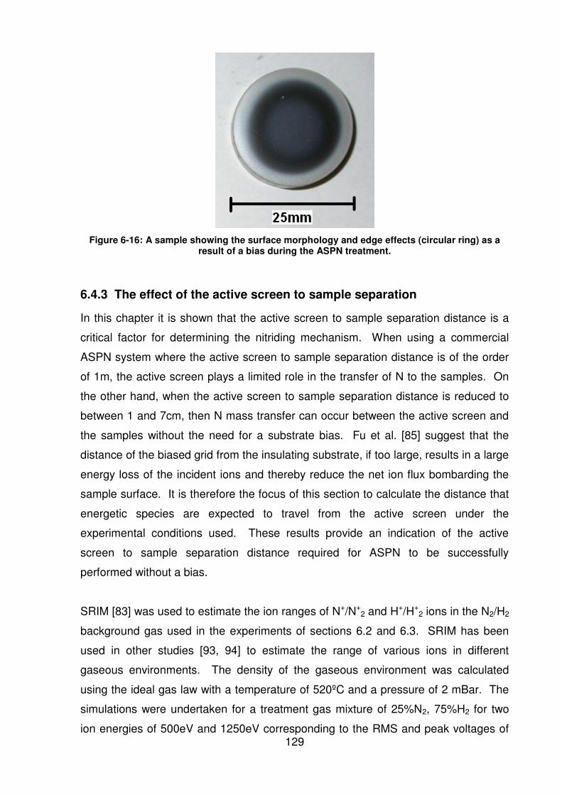
129
Figure 6-16: A sample showing the surface morphology and edge effects (circular ring) as a
result of a bias during the ASPN treatment.
6.4.3 The effect of the active screen to sample separation
In this chapter it is shown that the active screen to sample separation distance is a
critical factor for determining the nitriding mechanism. When using a commercial
ASPN system where the active screen to sample separation distance is of the order
of 1m, the active screen plays a limited role in the transfer of N to the samples. On
the other hand, when the active screen to sample separation distance is reduced to
between 1 and 7cm, then N mass transfer can occur between the active screen and
the samples without the need for a substrate bias. Fu et al. [85] suggest that the
distance of the biased grid from the insulating substrate, if too large, results in a large
energy loss of the incident ions and thereby reduce the net ion flux bombarding the
sample surface. It is therefore the focus of this section to calculate the distance that
energetic species are expected to travel from the active screen under the
experimental conditions used. These results provide an indication of the active
screen to sample separation distance required for ASPN to be successfully
performed without a bias.
SRIM [83] was used to estimate the ion ranges of N+/N+2 and H+/H+
2 ions in the N2/H2
background gas used in the experiments of sections 6.2 and 6.3. SRIM has been
used in other studies [93, 94] to estimate the range of various ions in different
gaseous environments. The density of the gaseous environment was calculated
using the ideal gas law with a temperature of 520ºC and a pressure of 2 mBar. The
simulations were undertaken for a treatment gas mixture of 25%N2, 75%H2 for two
ion energies of 500eV and 1250eV corresponding to the RMS and peak voltages of

130
the bias power supply signature at a 30% bias setting connected to the active screen.
The ion energies were halved (250eV, 625eV) in the simulation of the N+2 and H+
2
ions since SRIM does not allow molecular ions as incident ionic species. The results
of these simulations are shown in Figure 6-17 for the N+/N+2 ionic species and in
Figure 6-18 for the H+/H+2 ionic species. The results for the maximum distance
travelled of the N+/N+2 and ions H+/H+
2 are tabulated in Table 6-12.
Figure 6-17: The ion ranges for N
+ and N
+2 ions in a 25%N2, 75%H2 treatment gas mixture for
two bias settings. a) The N+ ion profile at 500V bias, b) The N
+ ion profile at 1250V bias, c) The
N+
2 ion profile at 500V bias, d) The N+
2 ion profile at 1250V bias.
a) b)
c) d)

131
Figure 6-18: The ion ranges for H+ and H
+2 ions in a 25%N2, 75%H2 treatment gas mixture for
two bias settings. a) The H+ ion profile at 500V bias, b) The H
+ ion profile at 1250V bias, c) The
H+
2 ion profile at 500V bias, d) The H+
2 ion profile at 1250V bias.
Ion Energy (eV) N+ N2+ H+ H2
+
500 47 23 180 100 1250 67 43 360 220
Table 6-12: Simulated values for the maximum ion range in mm of various ions in the 25%N2,
75%H2 treatment gas mixture for the two bias settings of 500V and 1250V.
The results indicate that the maximum distance travelled by the N+ ions in a
treatment gas mixture of 25%N2, 75%H2 is approximately 50mm for the 500V bias
and approximately 70mm for the 1250V bias conditions. This is an interesting result
since the results of the last section showed that as the distance of sample to screen
separation increased to around 70mm, the nitriding response in terms of the
hardness profiles is greatest within the experimental conditions investigated. The
a) b)
c) d)

132
results from SRIM support this and independently indicate that the range of the N+
ions under the experimental conditions investigated is sufficient to travel between the
active screen and the sample. These results suggest that the significant contributor
to the nitriding response in the mini screen treatments is the N+ ions, since the N+2
ions have a maximum ion range of 43mm according to SRIM. The ion ranges of both
the H+ and H+2 ions is much larger than the N+ and N+
2 ions as expected. Additional
calculations showed that the voltage on the active screen would need to be 50kV for
an N+ ion to travel 1m under the same process conditions. Furthermore, the
treatment gas pressure required to enable an N+ ion to travel 1.5m under a bias of
1250V was calculated to be 7x10⁻⁷ mBar. Implementing these parameters in the
commercial ASPN system employed in this study was not practicable.
The picture that emerges is that nitriding is a two stage process. Firstly, the transport
of nitrogen to the sample surface must occur. This can be achieved either by a
substrate bias or having a biased screen in close proximity to the sample surface. In
the latter case, the N species (either N ions or energetic N neutrals generated after
an N ion recombines with an electron) are accelerated through the open areas of the
mini active screen and impact the sample surface causing shallow N implantation in
the near surface region. Secondly, once an elevated nitrogen potential has occurred
at the sample surface, by either of the above mentioned methods, N diffusion occurs
into the subsurface region [42] giving rise to the diffusion zone and the hardening
response. Interestingly, despite the fact that screen material was shown to be
deposited on the sample surface during the nitriding treatment (see section 5.1.4) it
did not dramatically increase or inhibit the nitriding response. This result can be
explained since the deposited material is Fe rich and would not greatly restrict N
diffusion into the subsurface.
6.4.4 Summary
The results presented have shown that in ASPN, the distance between the sample
surface and the active screen is a critical factor in determining the nitriding response
of the materials investigated without a bias. It was shown that samples treated on
top of an insulating post and beneath the mini active screen at a separation of 12mm
could be successfully nitrided. The nitriding response was explained by considering

133
the use of biased grids to produce energetic N species which can bombard the
substrates.
To further understand the nitriding mechanism, a series of experiments were
undertaken in which varied the insulated sample to screen separation up to 70mm.
The results indicated that over the range investigated, the largest nitriding response
occurred for a sample to screen separation of 70mm. The results were supported by
using SRIM to estimate the ion range under the treatment conditions employed in
these experiments.
6.4.5 Conclusion
The variation of the nitriding response of a biased P20 steel showed no systematic
trend with height, up to 33 cm. This suggests that a commercial nitriding treatment of
a P20 steel should have a uniform nitriding response over its entire length, width and
breadth provided a sufficient bias voltage is applied during the nitriding treatment.
This result is basically an extension of the results presented in Chapter 4, where it
was shown that the nitriding response of a P20 steel, in terms of case depth, was
sufficient when a bias of 378V RMS was applied in this commercial ASPN system.
A comparison between the nitriding response for samples placed under a mini
screen, on an insulator and on the base showed that the nitriding response was
superior for the samples treated beneath the mini active screen. Furthermore, the
optimum separation between the samples and the mini active screen was 70mm for
the conditions investigated. A model is presented which can explain how a biased
screen surrounding the samples can generate energetic species which can efficiently
transfer N (either N ions or energetic N neutrals generated after an N ion recombines
with an electron) to the surface of the samples. This model was supported by SRIM
calculations which showed that the N+ ion range under the experimental conditions
analysed was of the order of 70mm. A major finding of this chapter was that it is
possible to successfully nitride samples with a mini screen in close proximity without
the need of a substrate bias, which is in agreement with previously published work
[48].

134
Chapter Seven
7 Conclusions and future work
7.1 The role of the active screen in ASPN
This study is the first thorough investigation of a commercial ASPN system.
Additionally, this thesis makes an important contribution to the understanding of the
mechanism that facilitates nitriding in ASPN. As a result, our understanding of ASPN
is now more complete.
The major findings of this thesis are:
1. When operated in the commercial mode, a substrate bias is essential
for successful nitriding of steels in terms of cross sectional hardness.
The level of substrate bias required is material dependent and depends
on the concentration of strong alloy nitride forming elements within the
steel.
2. It was shown that active screen material does get transferred to the
sample. However, no evidence was found that screen material mass
transfer had any positive affect on the nitriding response.
3. Surface hardness results alone were found to be insufficient to evaluate
the hardening response. Cross sectional hardness was found to be a
much more reliable method to determine that hardness response.
135
4. The distance between the active screen and the workload is critical in
facilitating nitrogen mass transfer during ASPN treatments. For small
active screen to sample separation distances, nitrogen mass transfer
can occur between the active screen and the samples in the form of
energetic ions or neutrals, allowing nitriding to occur without a substrate
bias. At large active screen to sample separations, as occurs in most
commercial systems, the active screen does not play a significant role
in N mass transfer to the samples and a substrate bias is essential to
achieve a satisfactory nitriding response.
Even though this study found that the active screen did not play a significant role in
the N mass transfer to the workload on the commercial scale, ASPN treatments have
notable benefits over DCPN treatments. Since ASPN uses the active screen to heat
the workload, the bias is not applied to the parts during the heating stage. In
comparison, DCPN treatments have the bias applied directly to the workload,
therefore using the plasma that surrounds the parts to be treated, the workload
attains the required nitriding temperature. The advantage of ASPN in this regard is
that the workload is not subject to sputtering of material and arcing damage during
this stage of the treatment where high power is applied to the parts.
It was found that the nitriding treatments of four steels, P20, H13, 4140 and 1020
under normal commercial conditions, produced large case depths only when a bias
was employed during the treatment. More specifically, in the case of P20, the bias
voltage was required to be of the order of 378V RMS (with a peak voltage of
approximately 1100V) and for H13 the bias voltage was required to be of the order of
540V RMS (with a peak voltage of approximately 1350V). To obtain a satisfactory
nitriding response after a commercial ASPN treatment of the steels investigated, a
sufficiently high bias must be applied. The treatment gas ratios were found to be a
less important parameter, with gas mixture treatments of 90% N2, 10% H2 and 5%
N2, 95% H2 producing similar surface and cross sectional hardness in P20 steel.

136
By using a HA active screen during the nitriding treatment, the deposited material on
the sample surface was identified to have originated from the active screen. Upon
further investigation with the use of Si substrates, the deposited material was found
to be in the form of nano particles. Interestingly, the bulk of the material transfer from
the active screen to the sample surface occurs during the heating stage of the
treatment cycle.
The results from the SRIM estimations for the maximum depth of penetration of ionic
H species having energy of 1250eV correlated with the depth of modification
observed from XTEM. It was shown that H ions are responsible for defects in the Si
substrate to depths of up to 150nm, however, this estimation only holds when
considering the high voltage pulses associated with the bias power supply signature.
To determine the effect of material transfer from the active screen to the sample
surface, a shield was utilised over one of two samples to reduce the direct line of
sight material transfer. With both of the samples at an equivalent bias potential, the
shielded sample responded with a larger case depth which indicated a higher
nitriding potential in comparison to the exposed sample. Based on this result, the
active screen sputter and deposition model proposed by Li et al. [48] is rejected as
the primary mechanism of N mass transfer in the ASPN system operating in its
normal commercial mode.
To further explore the effect of the active screen material deposition and the role of
the active screen on the nitriding response, a mini heater was used instead of the
active screen to heat the sample. The results revealed that a HH13 sample treated
using a 550V DC bias responded, however, a HH13 sample treated with a pulsed
bias on the base plate responded to a higher degree. This indicates that the level of
peak voltage is more likely to be the factor that determines the nitriding response
rather than active screen in this commercial ASPN system.
The nitriding response as a function of the distance between the sample surface and
the active screen was investigated with the results revealing that over the
experimental range studied, the nitriding response was invariant with height above
the base plate. However the experiment was conducted over a distance of 330mm
from the base plate where the nearest distance to the active screen was still of the
order of 1200mm at the highest point. Therefore the use of a mini active screen at a

137
separation of 12mm to the sample surface was investigated. These results were
then compared to the results from two other sets of samples which were placed
directly on the base and atop another insulator. The results of this analysis showed
that the electrically floating samples atop the insulating post and surrounded by the
mini active screen responded to a higher degree in terms of case depth compared to
the base samples and those atop the insulator. Therefore, electrically floating
samples can be nitrided in an ASPN environment provided the active screen is
sufficiently close to the sample surface. This phenomenon has been observed
previously in plasma immersion ion implantation experiments in which biased grids
are often used to treat insulating substrates. Furthermore, this result verifies part of
the study presented by Li et al. [48] where the nitriding treatment for a sample to
active screen separation of 12mm was successful. In order to determine the
optimum sample to active screen separation in terms of the nitriding response, a
series of experiments were undertaken at varying separations between the sample
surface and the mini active screen varied at values of 12mm, 20mm, 28mm, 50mm
and 70mm. These results combined with the SRIM estimations for the ion ranges
lead to the conclusion that N ions or neutrals are the primary mechanism for N mass
transfer in ASPN.
Through the course of this thesis, it has been demonstrated that in this commercial
ASPN system, a large case depth cannot be obtained unless a sufficient bias is
applied to the samples or the active screen is sufficiently close enough to the
electrically floating sample surface such that the N ion range is comparable to the
separation. In addition, it has been shown here that the nitriding potential can be
increased for a sample that is shielded from direct line of sight material transfer from
the active screen to the sample surface. Therefore, in order to produce a sufficient
hardness case depth in this commercial ASPN system, energetic bombardment is
required. This energetic bombardment can be generated by having a bias on the
samples or by having a bias on an active screen which is sufficiently close to the
electrically floating samples.
The debate about whether ions or neutral species are primarily responsible for the N
mass transfer to the sample surface can be reviewed in light of the results presented
in this thesis. Li et al. [48] proposed a modified sputter/deposition model that was
built on the early suggestion by Edenhofer [42] that N occlusion in DCPN was caused

138
by sputtering Fe (implied in his case form the steel parts being treated) and the
subsequent condensation of iron nitride on the surface. Li et al. [48] extended
Edenhofer’s [42] model for ASPN by pointing out that iron nitride (plus Fe and N) is
sputtered from the active screen, resulting in the transportation of iron nitride
particles through the ASPN system and their random deposition on the parts being
treated on the base plate. However, the results of this work indicate that the transfer
of active screen material to the sample surface does not assist the nitriding response.
Georges [9] suggested that in ASPN the principal species responsible for nitriding
are active neutral N. However, Georges [9] also states that for certain alloy
compositions, complicated part geometries and heavily loaded furnaces it is
desirable to apply a small cathodic potential to ensure uniform N mass transfer to the
parts to be treated. The results presented in this thesis clearly show that on the
commercial scale, ASPN treatments are only successful when a sufficient substrate
bias is applied to the samples. Therefore the primary mechanism for N mass transfer
under commercial conditions is ionic bombardment. However, when the separation
between the active screen and the sample surface is small, ASPN treatments of
electrically floating samples can produce a satisfactory nitriding response. It is
proposed that the mechanism of N mass transfer to the sample surface in this case is
energetic ions or neutrals originating from the active screen.

139
7.2 Future Work
Throughout the course of this research, several areas of interest, which have
tremendous research potential, have been identified. There may be merit in placing
a shield over the components to be treated under the active screen in order to reduce
the mass transfer of active screen material to the sample surface in this commercial
ASPN system, however, a sufficient bias must still be applied.
Furthermore, investigating the effects of nitriding time in this commercial ASPN
system may be worth pursuing. This is especially important during the early stages
of nitriding (within the first ten minutes) as the results of which may provide an insight
for ways to increase the uptake of N from the plasma environment to the sample
surface. This may take the form of alternating in situ plasma etching and nitriding
stages during the nitriding treatment in order to reduce the build up of surface oxides.
In terms of post discharge nitriding and the study presented by Ricard et al. [7, 8, 58],
in the authors opinion, a novel design could be implemented where the plasma is
generated by a gap type microwave power generator instead of the active screen.
One or more of these plasma type generators could then be incorporated into the
commercial ASPN system and a series of experiments could be devised to test the
nitriding response. The results of which could then be used to understand the
differences between the two systems.
To further investigate the role of the active screen, future studies could involve a
repeat of the mini heater experiment with the alteration of having the in built pulsed
DC power supply as the power source for the sample under test. With this
experimental arrangement, the effect of the active screen on the nitriding response
could be totally isolated. The experiment could then be expanded for multiple
sample materials which would give a broader understanding of the differences
between ASPN and DCPN in terms of the role of the active screen
In addition, an investigation could be undertaken to establish the origin of the high
concentrations of O2 within the ASPN system. This could take the form of using
optical emission spectroscopy in situ to determine if the source is from an inadequate

140
base pressure prior to the treatment cycle, or, contaminated treatment gas mixtures.
The latter could be from impure gas bottles or from leaks in the system.
Furthermore, an investigation involving a mini screen where the sample to mini
screen separation is further increased beyond 70mm would be warranted. In
addition, varying the mini screen open area fraction may provide an optimum open
area fraction value for a given mini screen to sample separation.
Several suggestions have been made to improve this commercial ASPN system.
The author believes that if these suggestions were realised in a commercial sense,
the nitriding performance in this commercial ASPN system could be improved, which
could lead to improved nitriding responses without the need for an applied bias.

141
7.3 References
[1] T. Bell, Metals and Materials (1991) 478.
[2] T. Bell, J. Phys, 25 (1992) 297.
[3] A.G. Gray, Source Book on Nitriding, American Society for Metals, Ohio, 1977.
[4] V. Korotchenko and T. Bell, In Heat Treatment '73 (1978) 107.
[5] T. Lampe, S. Eisenberg, and G. Laudien, Surf. Eng, 9(1) (1993) 69.
[6] J. Georges, PATENT - Nitriding Process and Nitriding Furnace Therefore,
Plasma Metal SA, United States Patent.
[7] A. Ricard, A. Pilorget, H. Michel, and M. Gantois, PATENT - Its in French -
See File
[8] A. Ricard, T. Czerwiec, T. Belmonte, S. Bockel, and H. Michel, Thin. Solid.
Films, 341(1-2) (1999) 1.
[9] J. Georges, Heat. Treat. Met, 28(no. 2) (2001) 33.
[10] A.S. Metals, ASM Metals Reference Book. 3rd ed, ed. M. Bauccio, ASM
International, Materials Park, Ohio, 1994.
[11] R.W. Cahn and P. Haasen, Physical Metallurgy. 4th ed, Elsevier Science B.V.,
Amsterdam, The Netherlands, 1996.
[12] A.S. Metals, ASM Handbook. 10th ed. Vol. 3, ASM International, Materials
Park, Ohio, 1992.
[13] E.A. Brandes and G.B. Brook, Smithells Metals Reference Book. 7th ed,
Butterworth Heinemann, Oxford, 1999.
[14] M.B. Karamis, Thin. Solid. Films, 217 (1992) 38.
[15] W. Kovacs and W. Russell, Ion Nitriding: Proceedings of an International
Conference on Ion Nitriding (1986) 9.
[16] K.H. Jack, Heat Treatment '73 (1973) 39.
[17] T. Bell, B.J. Birch, V. Korotchenko, and S.P. Evans, In Heat Treatment '73,
163 (1973) 51.
[18] B. Edenhofer, Met. Prog, 109 (1976) 38.
[19] B. Edenhofer, The Metallurgist and Material Technologist (1976) 421.
[20] T. Bell, B.J. Birch, V. Korotchenko, and S.P. Evans, In Heat Treatment '73,
163 (1975) 51.
[21] J. Michalski, Surf. Coat. Technol, 59(1-3) (1993) 321.
[22] E.J. Miola, S.D. de Souza, P.A.P. Nascente, M. Olzon-Dionysio, C.A. Olivieri,
and D. Spinelli, App. Surf. Sci, 144-145 (1999) 272.

142
[23] J. D'Haen, C. Quaeyhaegens, G. Knuyt, M. D'Olieslaeger, and L.M. Stals,
Surf. Coat. Technol, 74-75(Part 1) (1995) 405.
[24] M.A.J. Somers and E.J. Mittemeijer, Metallurgical and Materials Transactions
A, 26A (2005) 57.
[25] D.B. Clayton and K. Sachs, In Heat Treatment '73 (1976)
[26] B.J. Lightfoot and D.H. Jack, In Heat Treatment '73 (1973)
[27] D.A. Dashfield, In Heat Treatment '73 (1973)
[28] H. Du, L. Sproge, and J. Agren, Modeling of Nitrocarburizing, Proceeds of the
Second ASM, in "Heat Treatment and Surface Engineering", 1993.
[29] V.I. Dimitrov, J. D'Haen, G. Knuyt, C. Quaeyhaegens, and L.M. Stals, Comp.
Mat. Sci, 15(1) (1999) 22.
[30] A.U. Seybolt, Transactions of the Metallurgical Society of AIME, 245 (1969)
769.
[31] K.E. Thelning, Steel and its Heat Treatment, Butterworth, London, 1975.
[32] C.K. Jones, D.J. Sturges, and S.W. Martin, Met. Prog, 104 (1973) 62.
[33] A. Fry, ASST Nitriding Symposium (1929)
[34] V.O. Homerberg and J.P. Walsted, ASST Nitriding Symposium (1929)
[35] C.F. Floe, Trans. ASM, 32 (1944)
[36] R.L. Chenault and G.E. Mohnkern, Met. Prog (1953)
[37] Orica Australia Pty Ltd, Ammonia Handbook, 1 Nicholson Street, Melbourne,
Victoria, Australia.
[38] J.A. Camargo and A. Alonso, Environment International, 32(6) (2006) 831.
[39] E. Mitchell and C. Dawes, Met. Treat, 31 (1964) 3.
[40] P. Astley, In Heat Treatment '73, 163 (1973) 15.
[41] M.A. Lieberman and A.J. Lichtenberg, Principles of Plasma Discharges and
Meterials Processing. 2nd ed, Wiley Interscience, New Jersey, 2005.
[42] B. Edenhofer, Heat. Treat. Met, 1 (2) (1974) 23.
[43] C.K. Jones and S.W. Martin, Met. Prog, 85 (1964) 95.
[44] B. Edenhofer, Heat. Treat. Met, 2 (2) (1974) 59.
[45] C.K. Jones, S.W. Martin, D.J. Sturges, and M. Hudis, In Heat Treatment '73
(1973) 71.
[46] T. Bell and P.A. Dearnley, Surf. Eng, 10(2) (1994) 123.
[47] A. Brokman and F.R. Tuler, J. App. Phys, 52 (1981) 468.
[48] C.X. Li, T. Bell, and H. Dong, Surf. Eng, 18 (2002) 174.
[49] K. Keller, Harterei-Technische Mitteilungen (German), 26 (1971) 120.

143
[50] J. Kolbel, Forschungsberichte des Landes Nordhein-Westfalen, No. 1555.
West-deutscher Verlag, Koln. (German) (1965)
[51] J. Kolbel, Unpublished report from the Department of Physics of the Research
Institute of the "Gesellschaft zur Forderung der Glimment-ladungsforschung
e.V." (German) (1966)
[52] M. Hudis, J. App. Phys, 44 (1973) 1489.
[53] G.G. Tibbets, J. App. Phys, 45 (1974) 5072.
[54] K.-T. Rie, Surf. Coat. Technol, 112(1-3) (1999) 56.
[55] Y. Sun and T. Bell, Mater. Sci. Eng. A, 224(1-2) (1997) 33.
[56] A. Sokolowska, J. Rudnicki, P. Beer, L. Maldzinski, J. Tacikowski, and J.
Baszkiewicz, Surf. Coat. Technol, 142-144 (2001) 1040.
[57] T. Czerwiec, H. Michel, and E. Bergmann, Surf. Coat. Technol, 108-109(1-3)
(1998) 182.
[58] A. Ricard, J. Deschamps, J.L. Godard, L. Falk, and H. Michel, Mater. Sci. Eng.
A, 139 (1991) 9.
[59] H. Malvos, A. Ricard, J. Szekely, H. Michel, M. Gantois, and D. Ablitzer, Surf.
Coat. Technol, 59(1-3) (1993) 59.
[60] C.X. Li and T. Bell, Cor. Sci, 46(6) (2004) 1527.
[61] C.X. Li and T. Bell, Wear, 256(11-12) (2004) 1144.
[62] C. Zhao, C.X. Li, H. Dong, and T. Bell, Surf. Coat. Technol, 201(6) (2006)
2320.
[63] S. Ahangarani, F. Mahboubi, and A.R. Sabour, Vacuum, 80 (2006) 1032.
[64] J. Alves, C., F.O. de Araujo, K.J.B. Ribeiro, J.A.P. da Costa, R.R.M. Sousa,
and R.S. de Sousa, Surf. Coat. Technol, 201(6) (2006) 2450.
[65] C. Alves Jr, private communication (2007) 29th June.
[66] Bohler Uddeholm Australia Pty Ltd, in Poster of Metal Chemical Composition,
282-290 Greens Road, Dandenong, Victoria, Australia.
[67] R. Payling, Spectroscopy, 13(1) (1998) 36.
[68] R. Payling, D.G. Jones, and A. Bengtson, Glow Discharge Optical Emission
Spectrometry, John Wiley & Sons, Chichester, UK, 1997.
[69] J. Long, Proceedings of Engineering Materials, Melbourne (2001) 23.
[70] R. Payling and P. Larkins, Optical Emission Lines of the Elements, John Wiley
& Sons, Chichester, UK, 2000.
[71] D.B. Williams and C.B. Carter, Transmission Electron Microscopy, Plenum
Press, USA, 1996.

144
[72] B.D. Cullity and S.R. Stock, Elements of X-RAY DIFFRACTION. 3rd ed,
Addison-Wesley Publishing Company, 2001.
[73] G.M. Clarke, Introduction to the Design and Analysis of Experiments, Arnold,
1997.
[74] D.H. Jack and I.M. Stoney, Scand. J. Metall, 1 (1972) 217.
[75] D.H. Jack, P.C. Lidster, P. Grieveson, and K.H. Jack, Chem. Metall. Iron. Steel
(1973) 374.
[76] D.R. Lide, Handbook of Chemistry and Physics. 79th ed, CRC Press, New
York, 1999.
[77] P.C. Jindal, J. Vac. Sci. Technol, 15(2) (1977) 313.
[78] E.J. Miola, S.D. de Souza, P.A.P. Nascente, M. Olzon-Dionysio, C.A. Olivieri,
and D. Spinelli, J. Vac. Sci. Technol, 18(6) (2000) 2733.
[79] W.D.J. Callister, Materials Science and Engineering an Introduction. 4th ed,
John Wiley & Sons Inc, 1996.
[80] N.M. Hwang, J. Cryst. Growth, 135(1-2) (1994) 165.
[81] S.J. Jeng, G.S. Oehrlein, and G.J. Scilla, Appl. Phys. Lett, 53 (1988) 1735.
[82] S. Muto, S. Takeda, and M. Hirata, Philosophical Magazine A, 72(4) (1995)
1057.
[83] J.F. Ziegler, M.D. Ziegler, and J.P. Biersack, The Stopping and Range of Ions
in Matter, Pergamon, New York.
[84] A.J. Bourdillon, S.J. Bull, P.J. Burnett, and T.F. Page, J. Mater. Sci, 21 (1986)
1547.
[85] R.K.Y. Fu, K.L. Fu, X. Tian, and P.K. Chu, J. Vac. Sci. Technol, 22(2) (2004)
356.
[86] F. Liu, M.R. Dickinson, R.A. Macgill, A. Anders, O.R. Monteiro, I.G. Brown, L.
Phillips, G. Biallas, and T. Siggins, Surf. Coat. Technol, 103 (1998) 46.
[87] F. Deng, R.A. Johnson, P.M. Asbeck, S.S. Lau, W.B. Dubbelday, T. Hsiao,
and J. Woo, J. Appl. Phys., 81(12) (1997) 8047.
[88] W.J. Chen and L.J. Chen, J. Appl. Phys., 70(5) (1991) 2628.
[89] V. Teodorescu, L. Nistor, H. Bender, A. Steegen, A. Lauwers, K. Maex, and J.
Van Landuyt, J. Appl. Phys., 90(1) (2001) 167.
[90] X.B. Tian, K.Y. Fu, P.K. Chu, and S.Q. Yang, Surf. Coat. Technol, 196(1-3)
(2005) 162.
[91] R.K.Y. Fu, X. Tian, and P.K. Chu, Rev. Sci. Instrum, 74(8) (2003) 3697.

145
[92] M.M.M. Bilek, R.C. Powels, and D.R. McKenzie, Biomaterials and Surface
Modification. 1st ed, In Press, 2007.
[93] P.K. Diwan, S. Kumar, G. Singh, and L. Singh, Radiat. Meas, 33(2) (2001)
193.
[94] U. Greife, S. Bishop, L. Buchmann, M.L. Chatterjee, A.A. Chen, J.M. D'Auria,
S. Engel, D. Gigliotti, D. Hunter, D.A. Hutcheon, A. Hussein, C.C. Jewett, A.M.
Laird, M. Lamey, W. Liu, A. Olin, D. Ottewell, J. Rogers, and C. Wrede, Nucl.
Inst. Meth. Phys. Res. B, 217(1) (2004) 1.