chapter 46 mipi d-phy 46.1 overviewrockchip.fr/rk312x trm/chapter-46-mipi-d-phy.pdf · chapter 46...
TRANSCRIPT

RK3128 Technical Reference Manual Rev 1.0
High Performance and Low-power Processor for Digital Media Application 1535
Chapter 46 MIPI D-PHY
46.1 Overview
The MIPI D-PHY integrates a MIPI® V1.0 compatible PHY that supports up to 1GHz high speed data receiver, plus a MIPI® low-power low speed transceiver
that supports data transfer in the bi-directional mode. It supports the full
specifications described in V1.0 of the D-PHY spec. The D-PHY is built in with a standard digital interface to talk to MIPI Host controller. The architecture
supports connection of multiple data lanes in parallel – up to 4 data lanes can be
connected to increase the total through-put, customizable to user
determinedconfigurations.TheMIPI D-PHY supports the electrical portion of MIPI D-PHY V1.0 standard, covering all transmission modes (ULP/LP/HS).
The MIPI D-PHYsupports the following features:
Mixed-signal D-PHY mixed-signal hard-macro- LS Transmitter and LS/HS Receiver solution
Designed to MIPI® v1.0 Specifications
Integrated PHY Protocol Interface (PPI) supports interface to CSI, DSI and UniPro™ MIPI® protocols
1.0GHz maximum data transfer rate per lane
Expandable to support 4 data lanes, providing up to 4Gbps transfer rate HS, LP and ULPS modes supported
10Mbps per lane in low-power mode
Unidirectional and bi-directional modes supported Automatic termination control for HS and LP modes
Low-Power dissipation: HS less than 3mA/Lane
Tx/Rx Buffers with tunable On-Die-Termination and advanced equalization. Embedded ESD, boundary scan support logic.
46.2 Block Diagram
The MIPI D-PHY configuration contains one Clock Lane Module and four Data
Lane Modules. Each of these PHY Lane Modules communicates via two Lines to
a complementary part at the other side of the Lane Interconnect. The following diagram shows the D-PHY architecture.

RK3128 Technical Reference Manual Rev 1.0
High Performance and Low-power Processor for Digital Media Application 1536
D-PHYMaster Clock Lane Module
D-PHYMaster Data Lane Module
D-PHYMaster Data Lane Module
D-PHYSlave Clock Lane Module
D-PHYSlave Data Lane Module
D-PHYSlave Data Lane Module
D-PHYMaster Data Lane Module
D-PHYMaster Data Lane Module
D-PHYSlave Data Lane Module
D-PHYSlave Data Lane Module
PPI
PPI
PPI
PPI
PPI
PPI
PPI
PPI
PPI
PPIPHY
AdapterLayer
APPI
PHYAdapterLayer
APPI
ClockMultiplier
Unit
QIRef Clock
Controls
PHY PHY
Master Side Slave Side Fig.46-1MIPI D-PHY simplified Block diagram with master to slave
The following diagram shows a Universal Lane Module Diagram with a global
overview of internal functionality of the CIL function. This Universal Module can be used for all Lane types. The requirements for the ‘Control and Interface Logic’
(CIL) function depend on the Lane type and Lane side.
TX Ctrl Logic
Esc Encoder
DataIF
logic HS-Serialize
Sequences
HS-DeserializeData
Sampler
Esc Decoder
Ctrl Decoder
CtrlIF
logicState Machine
(incl Enables,Selects
and System Ctrl)
Error detect
Data In
Data Out
Clocks-in
Clocks-out
Control-in
Control-out
PPI(appendix)
ProtocolSide Line Control &Interface Logic
LP-TX
HS-TX
HS-RX Rt
LP-RX
LP-CD
Line Side
CD
RX
TX
Dp
Dn
Fig.46-2MIPI D-PHY V1.0 detailed block diagram

RK3128 Technical Reference Manual Rev 1.0
High Performance and Low-power Processor for Digital Media Application 1537
46.3 Function Description
The MIPI D-PHY transceiver is designed to reliably transmit HS and LP/ULP
data/clock over the channel and recover the MIPI LP data stream from any MIPI
input signal. It consists of 4 data transceiver paths and 1 clock transmitting path. For each data lane a HS transmitter and a LP transceiver is necessary to
transmit/recover the data streams, for the clock lane, a HS/LP transmitter is
designed to output the high speed clock signal over the channel.
A HS differential signal driven on the Dp and Dn pins is generated by a
differential output driver. For reference, Dp is considered as the positive side
and Dn as the negative side. High speed current switches are designed to output data streams over the channels.
The Low-Power receiver is an un-terminated, single-ended receiver circuit. LP receiver is used to detect the Low-Power state on each pin. For high robustness,
the LP receiver can filter out noise pulses and RF interference. Furthermore, any
spikes with a pulse width smaller than 20ns will be rejected.
Contention Detector (LP-CD) is designed in Data Lane to monitor the line
voltage on each Low-Power signal. The LP-CD is used to detect an LP low fault when the LP transmitter is driving low and the pin voltage is greater than
450mV.
The Low-Power transmitter is a slew-rate controlled push-pull driver. The
minimum pull-down and pull-up impedance of LP driver is 110 ohm. At the same
time tunable slew rate control logic is available for eye pattern requirement. .
46.4 Register Description
This section describes the control/status registers of the design. While you are
reading this chapter please note that the offset address[7:0] is distributed two
parts, one from the bit7 to bit5 is the first address, the other from the bit4 to
bit0 is the second address. When you configure the registers, you must set both of them. The Clock Lane and Data Lane use the same registers with the same
second address, but the first address is different.Itsapb base address is 0xc00.

RK3128 Technical Reference Manual Rev 1.0
High Performance and Low-power Processor for Digital Media Application 1538
46.4.1 Register Summary
Name Offset Size Reset
Value Description
MIPIPHY_REG0 0x0000 W 0x00000001 mipiphy register 0
MIPIPHY_REG1 0x0004 W 0x00000003 mipiphy register 1
MIPIPHY_REG3 0x000c W 0x00000003 mipiphy register 3
MIPIPHY_REG4 0x0010 W 0x0000007d mipiphy register 4
MIPIPHY_REG20 0x0080 W 0x00000001 mipiphy register 20
MIPIPHY_REG40 0x0100 W 0x0000000b mipiphy register 40
MIPIPHY_REG45 0x0114 W 0x00000005 mipiphy register 45
MIPIPHY_REG46 0x0118 W 0x00000000 mipiphy register 46
MIPIPHY_REG47 0x011c W 0x00000000 mipiphy register 47
MIPIPHY_REG48 0x0120 W 0x00000000 mipiphy register 48
MIPIPHY_REG49 0x0124 W 0x00000000 mipiphy register 49
MIPIPHY_REG4A 0x0128 W 0x00000000 mipiphy register 4a
MIPIPHY_REG4B 0x012c W 0x00000000 mipiphy register 4b
MIPIPHY_REG4C 0x0130 W 0x00000000 mipiphy register 4c
MIPIPHY_REG4D 0x0134 W 0x00000000 mipiphy register 4d
MIPIPHY_REG4E 0x0138 W 0x00000000 mipiphy register 4e
MIPIPHY_REG50 0x0140 W 0x00000000 mipiphy register 50
MIPIPHY_REG51 0x0144 W 0x00000000 mipiphy register 51
MIPIPHY_REG52 0x0148 W 0x00000000 mipiphy register 52
MIPIPHY_REG60 0x0180 W 0x0000000b mipiphy register 60
MIPIPHY_REG65 0x0194 W 0x00000005 mipiphy register 65
MIPIPHY_REG66 0x0198 W 0x00000000 mipiphy register 66
MIPIPHY_REG67 0x019c W 0x00000000 mipiphy register 67
MIPIPHY_REG68 0x01a0 W 0x00000000 mipiphy register 68
MIPIPHY_REG69 0x01a4 W 0x00000000 mipiphy register 69
MIPIPHY_REG6A 0x01a8 W 0x00000000 mipiphy register 6a
MIPIPHY_REG6B 0x01ac W 0x00000000 mipiphy register 6b
MIPIPHY_REG6C 0x01b0 W 0x00000000 mipiphy register 6c
MIPIPHY_REG6D 0x01b4 W 0x00000000 mipiphy register 6d
MIPIPHY_REG6E 0x01b8 W 0x00000000 mipiphy register 6e
MIPIPHY_REG70 0x01c0 W 0x00000000 mipiphy register 70
MIPIPHY_REG71 0x01c4 W 0x00000000 mipiphy register 71
MIPIPHY_REG72 0x01c8 W 0x00000000 mipiphy register 72
MIPIPHY_REG80 0x0200 W 0x0000000b mipiphy register 80
MIPIPHY_REG85 0x0214 W 0x00000005 mipiphy register 85
MIPIPHY_REG86 0x0218 W 0x00000000 mipiphy register 86
MIPIPHY_REG87 0x021c W 0x00000000 mipiphy register 87
MIPIPHY_REG88 0x0220 W 0x00000000 mipiphy register 88
MIPIPHY_REG89 0x0224 W 0x00000000 mipiphy register 89
MIPIPHY_REG8A 0x0228 W 0x00000000 mipiphy register 8a
MIPIPHY_REG8B 0x022c W 0x00000000 mipiphy register 8b
MIPIPHY_REG8C 0x0230 W 0x00000000 mipiphy register 8c
MIPIPHY_REG8D 0x0234 W 0x00000000 mipiphy register 8d
MIPIPHY_REG8E 0x0238 W 0x00000000 mipiphy register 8e
MIPIPHY_REG90 0x0240 W 0x00000000 mipiphy register 90
MIPIPHY_REG91 0x0244 W 0x00000000 mipiphy register 91
MIPIPHY_REG92 0x0248 W 0x00000000 mipiphy register 92

RK3128 Technical Reference Manual Rev 1.0
High Performance and Low-power Processor for Digital Media Application 1539
Name Offset Size Reset Value
Description
MIPIPHY_REGA0 0x0280 W 0x0000000b mipiphy register a0
MIPIPHY_REGA5 0x0294 W 0x00000005 mipiphy register a5
MIPIPHY_REGA6 0x0298 W 0x00000000 mipiphy register a6
MIPIPHY_REGA7 0x029c W 0x00000000 mipiphy register a7
MIPIPHY_REGA8 0x02a0 W 0x00000000 mipiphy register a8
MIPIPHY_REGA9 0x02a4 W 0x00000000 mipiphy register a9
MIPIPHY_REGAA 0x02a8 W 0x00000000 mipiphy register aa
MIPIPHY_REGAB 0x02ac W 0x00000000 mipiphy register ab
MIPIPHY_REGAC 0x02b0 W 0x00000000 mipiphy register ac
MIPIPHY_REGAD 0x02b4 W 0x00000000 mipiphy register ad
MIPIPHY_REGAE 0x02b8 W 0x00000000 mipiphy register ae
MIPIPHY_REGB0 0x02c0 W 0x00000000 mipiphy register b0
MIPIPHY_REGB1 0x02c4 W 0x00000000 mipiphy register b1
MIPIPHY_REGB2 0x02c8 W 0x00000000 mipiphy register b2
MIPIPHY_REGC0 0x0300 W 0x0000000b mipiphy register c0
MIPIPHY_REGC5 0x0314 W 0x00000005 mipiphy register c5
MIPIPHY_REGC6 0x0318 W 0x00000000 mipiphy register c6
MIPIPHY_REGC7 0x031c W 0x00000000 mipiphy register c7
MIPIPHY_REGC8 0x0320 W 0x00000000 mipiphy register c8
MIPIPHY_REGC9 0x0324 W 0x00000000 mipiphy register c9
MIPIPHY_REGCA 0x0328 W 0x00000000 mipiphy register ca
MIPIPHY_REGCB 0x032c W 0x00000000 mipiphy register cb
MIPIPHY_REGCC 0x0330 W 0x00000000 mipiphy register cc
MIPIPHY_REGCD 0x0334 W 0x00000000 mipiphy register cd
MIPIPHY_REGCE 0x0338 W 0x00000000 mipiphy register ce
MIPIPHY_REGD0 0x0340 W 0x00000000 mipiphy register d0
MIPIPHY_REGD1 0x0344 W 0x00000000 mipiphy register d1
MIPIPHY_REGD2 0x0348 W 0x00000000 mipiphy register d2
MIPIPHY_REGE0 0x0380 W 0x00000000 mipiphy register e0
MIPIPHY_REGEA 0x03A8 W 0x00000000 mipiphy register ea Notes:Size:B- Byte (8 bits) access, HW- Half WORD (16 bits) access, W-WORD (32 bits) access
46.4.2 Detail Register Description
MIPIPHY_REG0
Address: Operational Base + offset (0x0000)
mipiphy register 0
Bit Attr Reset Value Description
31:7 RO 0x0 reserved
6 RW 0x0 lane_en_ck 1: enable
0: disable
5 RW 0x0
lane_en_3
1: enable
0: disable
4 RW 0x0 lane_en_2 1: enable
0: disable
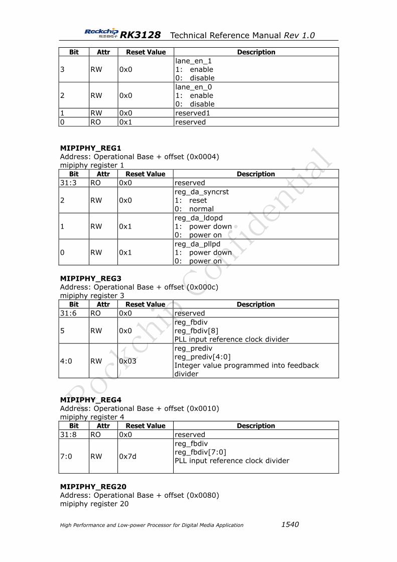
RK3128 Technical Reference Manual Rev 1.0
High Performance and Low-power Processor for Digital Media Application 1540
Bit Attr Reset Value Description
3 RW 0x0
lane_en_1
1: enable
0: disable
2 RW 0x0 lane_en_0 1: enable
0: disable
1 RW 0x0 reserved1
0 RO 0x1 reserved
MIPIPHY_REG1
Address: Operational Base + offset (0x0004) mipiphy register 1
Bit Attr Reset Value Description
31:3 RO 0x0 reserved
2 RW 0x0
reg_da_syncrst
1: reset
0: normal
1 RW 0x1
reg_da_ldopd
1: power down 0: power on
0 RW 0x1 reg_da_pllpd 1: power down
0: power on
MIPIPHY_REG3 Address: Operational Base + offset (0x000c)
mipiphy register 3
Bit Attr Reset Value Description
31:6 RO 0x0 reserved
5 RW 0x0
reg_fbdiv
reg_fbdiv[8]
PLL input reference clock divider
4:0 RW 0x03
reg_prediv reg_prediv[4:0]
Integer value programmed into feedback
divider
MIPIPHY_REG4
Address: Operational Base + offset (0x0010)
mipiphy register 4
Bit Attr Reset Value Description
31:8 RO 0x0 reserved
7:0 RW 0x7d
reg_fbdiv reg_fbdiv[7:0]
PLL input reference clock divider
MIPIPHY_REG20 Address: Operational Base + offset (0x0080)
mipiphy register 20

RK3128 Technical Reference Manual Rev 1.0
High Performance and Low-power Processor for Digital Media Application 1541
Bit Attr Reset Value Description
31:1 RO 0x0 reserved
0 RW 0x1
reg_dig_rstn
1: normal
0: reset
MIPIPHY_REG40
Address: Operational Base + offset (0x0100) mipiphy register 40
Bit Attr Reset Value Description
31:4 RO 0x0 reserved
3:0 RW 0xb
reg_ths_settle
Clock Lane
Configure the count time of the THS-SETTLE by protocol.
After the count done, D-PHY will begin to
receive the high speed data. (Can be configured from 4'h0 to 4'hd)
4'b0000 80-110 MHz
4'b0001 110-150 MHz
4'b0010 150-200 MHz 4'b0011 200-250 MHz
4'b0100 250-300 MHz
4'b0101 300-400 MHz 4'b0110 400-500 MHz
4'b0111 500-600 MHz
4'b1000 600-700 MHz 4'b1001 700-800 MHz
4'b1010 800-1000 MHz
4'b1011 additional adjust 4'b1100 additional adjust
4'b1101 additional adjust
4'b1110 additional adjust
MIPIPHY_REG45
Address: Operational Base + offset (0x0114) mipiphy register 45
Bit Attr Reset Value Description
31:6 RO 0x0 reserved
5:0 RW 0x05
reg_hs_tlpx
Clock Lane
The value of counter for HS Tlpx Time (>=Tlpx)
= Tpin_txbyteclkhs * value
MIPIPHY_REG46
Address: Operational Base + offset (0x0118) mipiphy register 46
Bit Attr Reset Value Description

RK3128 Technical Reference Manual Rev 1.0
High Performance and Low-power Processor for Digital Media Application 1542
Bit Attr Reset Value Description
31:7 RO 0x0 reserved
6:0 RW 0x00
reg_hs_ths_prepare
Clock Lane
The value of counter for HS Ths-prepare For clock lane, Ths-prepare(38ns~95ns)
For data lane,
Ths-prepare(40ns+4UI~85ns+6UI) =Ttxddrclkhs*value
MIPIPHY_REG47 Address: Operational Base + offset (0x011c)
mipiphy register 47
Bit Attr Reset Value Description
31:6 RO 0x0 reserved
5:0 RW 0x00
reg_hs_the_zero
Clock Lane The value of counter for HS Ths-zero
For clock lane, Ths-prepare+Ths-zero
(>=300ns)
For data lane, Ths-prepare+Ths-zero (>= 145 ns + 10*UI)
= Tpin_txbyteclkhs*value
For clock lane, S_HSTXTHSZERO[5:0] = 6'b100000
For data lane, S_HSTXTHSZERO[5:0] =
6'b001001 Frequency(1/UI) Value(Decimal)
80 -110 MHz 3
110-150 MHz 4 150-200 MHz 4
200-250 MHz 5
250-300 MHz 6 300-400 MHz 7
400-500 MHz 8
500-600 MHz 10 600-700 MHz 11
700-800 MHz 12
800-1000 MHz 15
MIPIPHY_REG48 Address: Operational Base + offset (0x0120)
mipiphy register 48
Bit Attr Reset Value Description
31:7 RO 0x0 reserved

RK3128 Technical Reference Manual Rev 1.0
High Performance and Low-power Processor for Digital Media Application 1543
Bit Attr Reset Value Description
6:0 RW 0x00
reg_hs_ths_trail
Clock Lane
The value of counter for HS Ths-trail For clock lane, Ths-trail (>=60ns)
For data lane,Ths-trail (>=max(8UI,
60ns+4UI) = Tad_txddrclkhs_i* value
For clock lane, S_HXTXTHSTRAIL[6:0] =
7'b0100111 For data lane, S_HXTXTHSTRAIL[6:0] =
7'b0100111
Frequency(1/UI) Value(Decimal) 80 -110 MHz 12
110-150 MHz 13
150-200 MHz 17 200-250 MHz 20
250-300 MHz 24
300-400 MHz 29 400-500 MHz 35
500-600 MHz 41
600-700 MHz 49
700-800 MHz 52 800-1000 MHz 64
MIPIPHY_REG49
Address: Operational Base + offset (0x0124)
mipiphy register 49
Bit Attr Reset Value Description
31:5 RO 0x0 reserved
4:0 RW 0x00
reg_hs_ths_exit
Clock Lane The value of counter for HS Ths-exit
Ths-exit
= Tpin_txbyteclkhs*value
MIPIPHY_REG4A Address: Operational Base + offset (0x0128)
mipiphy register 4a
Bit Attr Reset Value Description
31:4 RO 0x0 reserved
3:0 RW 0x0
reg_hs_tclk_post
Clock Lane
The value of counter for HS Tclk-post Tclk-post =Tpin_txbyteclkhs*value
MIPIPHY_REG4B
Address: Operational Base + offset (0x012c)

RK3128 Technical Reference Manual Rev 1.0
High Performance and Low-power Processor for Digital Media Application 1544
mipiphy register 4b
Bit Attr Reset Value Description
31:8 RO 0x0 reserved
7:0 RW 0x00 reserved
MIPIPHY_REG4C Address: Operational Base + offset (0x0130)
mipiphy register 4c
Bit Attr Reset Value Description
31:2 RO 0x0 reserved
1:0 RW 0x0
reg_hs_twakup
Clock Lane The value[9:8] of counter for HS Twakup
also see REG4D
MIPIPHY_REG4D Address: Operational Base + offset (0x0134)
mipiphy register 4d
Bit Attr Reset Value Description
31:8 RO 0x0 reserved
7:0 RW 0x00
reg_hs_twakup Clock Lane
The value[7:0] of counter for HS Twakup
Twakup for ulpm, Twakup
= Tpin_sys_clk*value[9:0]
MIPIPHY_REG4E
Address: Operational Base + offset (0x0138)
mipiphy register 4e
Bit Attr Reset Value Description
31:4 RO 0x0 reserved
3:0 RW 0x0
reg_hs_tclk_pre Clock Lane
The value of counter for HS Tclk-pre
Tclk-pre for clock lane Tclk-pre
= Tpin_txbyteclkhs*value
MIPIPHY_REG50
Address: Operational Base + offset (0x0140)
mipiphy register 50
Bit Attr Reset Value Description
31:6 RO 0x0 reserved

RK3128 Technical Reference Manual Rev 1.0
High Performance and Low-power Processor for Digital Media Application 1545
Bit Attr Reset Value Description
5:0 RW 0x00
reg_hs_tta_go
Clock Lane
The value of counter for HS Tta-go Tta-go for turnaround
Tta-go
= Ttxclkesc*value
MIPIPHY_REG51
Address: Operational Base + offset (0x0144) mipiphy register 51
Bit Attr Reset Value Description
31:6 RO 0x0 reserved
5:0 RW 0x00
reg_hs_tta_sure
Clock Lane
The value of counter for HS Tta-sure Tta-sure for turnaround
Tta-sure
= Ttxclkesc*value
MIPIPHY_REG52
Address: Operational Base + offset (0x0148) mipiphy register 52
Bit Attr Reset Value Description
31:6 RO 0x0 reserved
5:0 RW 0x00
reg_hs_tta_wait
Clock Lane
The value of counter for HS Tta-wait Tta-wait for turnaround
Interval from receiving ppi turnaround request
to sending esc request. Tta-wait
= Ttxclkesc*value
MIPIPHY_REG60
Address: Operational Base + offset (0x0180)
mipiphy register 60
Bit Attr Reset Value Description
31:4 RO 0x0 reserved

RK3128 Technical Reference Manual Rev 1.0
High Performance and Low-power Processor for Digital Media Application 1546
Bit Attr Reset Value Description
3:0 RW 0xb
reg_ths_settle
Data0 Lane
Configure the count time of the THS-SETTLE by protocol.
After the count done, D-PHY will begin to
receive the high speed data. (Can be configured from 4'h0 to 4'hd)
4'b0000 80-110 MHz
4'b0001 110-150 MHz 4'b0010 150-200 MHz
4'b0011 200-250 MHz
4'b0100 250-300 MHz 4'b0101 300-400 MHz
4'b0110 400-500 MHz
4'b0111 500-600 MHz 4'b1000 600-700 MHz
4'b1001 700-800 MHz
4'b1010 800-1000 MHz 4'b1011 additional adjust
4'b1100 additional adjust
4'b1101 additional adjust
4'b1110 additional adjust
MIPIPHY_REG65 Address: Operational Base + offset (0x0194)
mipiphy register 65
Bit Attr Reset Value Description
31:6 RO 0x0 reserved
5:0 RW 0x05
reg_hs_tlpx
Data0 Lane
The value of counter for HS Tlpx Time (>=Tlpx)
= Tpin_txbyteclkhs * value
MIPIPHY_REG66 Address: Operational Base + offset (0x0198)
mipiphy register 66
Bit Attr Reset Value Description
31:7 RO 0x0 reserved
6:0 RW 0x00
reg_hs_ths_prepare
Data0 Lane The value of counter for HS Ths-prepare
For clock lane, Ths-prepare(38ns~95ns)
For data lane,
Ths-prepare(40ns+4UI~85ns+6UI) =Ttxddrclkhs*value
MIPIPHY_REG67

RK3128 Technical Reference Manual Rev 1.0
High Performance and Low-power Processor for Digital Media Application 1547
Address: Operational Base + offset (0x019c)
mipiphy register 67
Bit Attr Reset Value Description
31:6 RO 0x0 reserved
5:0 RW 0x00
reg_hs_the_zero Data0 Lane
The value of counter for HS Ths-zero
For clock lane, Ths-prepare+Ths-zero (>=300ns)
For data lane, Ths-prepare+Ths-zero (>= 145
ns + 10*UI)
= Tpin_txbyteclkhs*value For clock lane, S_HSTXTHSZERO[5:0] =
6'b100000
For data lane, S_HSTXTHSZERO[5:0] = 6'b001001
Frequency(1/UI) Value(Decimal)
80 -110 MHz 3 110-150 MHz 4
150-200 MHz 4
200-250 MHz 5 250-300 MHz 6
300-400 MHz 7
400-500 MHz 8 500-600 MHz 10
600-700 MHz 11
700-800 MHz 12 800-1000 MHz 15
MIPIPHY_REG68 Address: Operational Base + offset (0x01a0)
mipiphy register 68
Bit Attr Reset Value Description
31:7 RO 0x0 reserved

RK3128 Technical Reference Manual Rev 1.0
High Performance and Low-power Processor for Digital Media Application 1548
Bit Attr Reset Value Description
6:0 RW 0x00
reg_hs_ths_trail
Data0 Lane
The value of counter for HS Ths-trail For clock lane, Ths-trail (>=60ns)
For data lane,Ths-trail (>=max(8UI,
60ns+4UI) = Tad_txddrclkhs_i* value
For clock lane, S_HXTXTHSTRAIL[6:0] =
7'b0100111 For data lane, S_HXTXTHSTRAIL[6:0] =
7'b0100111
Frequency(1/UI) Value(Decimal) 80 -110 MHz 12
110-150 MHz 13
150-200 MHz 17 200-250 MHz 20
250-300 MHz 24
300-400 MHz 29 400-500 MHz 35
500-600 MHz 41
600-700 MHz 49
700-800 MHz 52 800-1000 MHz 64
MIPIPHY_REG69 Address: Operational Base + offset (0x01a4)
mipiphy register 69 Bit Attr Reset Value Description
31:5 RO 0x0 reserved
4:0 RW 0x00
reg_hs_ths_exit
Data0 Lane The value of counter for HS Ths-exit
Ths-exit
= Tpin_txbyteclkhs*value
MIPIPHY_REG6A Address: Operational Base + offset (0x01a8)
mipiphy register 6a
Bit Attr Reset Value Description
31:4 RO 0x0 reserved
3:0 RW 0x0
reg_hs_tclk_post
Data0 Lane
The value of counter for HS Tclk-post Tclk-post =Tpin_txbyteclkhs*value
MIPIPHY_REG6B
Address: Operational Base + offset (0x01ac)

RK3128 Technical Reference Manual Rev 1.0
High Performance and Low-power Processor for Digital Media Application 1549
mipiphy register 6b Bit Attr Reset Value Description
31:8 RO 0x0 reserved
7:0 RW 0x00
reserved
Data0 Lane reserved
MIPIPHY_REG6C
Address: Operational Base + offset (0x01b0) mipiphy register 6c
Bit Attr Reset Value Description
31:2 RO 0x0 reserved
1:0 RW 0x0
reg_hs_twakup
Data0 Lane
The value[9:8] of counter for HS Twakup also see REG6D
MIPIPHY_REG6D Address: Operational Base + offset (0x01b4)
mipiphy register 6d
Bit Attr Reset Value Description
31:8 RO 0x0 reserved
7:0 RW 0x00
reg_hs_twakup
Data0 Lane The value[7:0] of counter for HS Twakup
Twakup for ulpm,
Twakup = Tpin_sys_clk*value[9:0]
MIPIPHY_REG6E Address: Operational Base + offset (0x01b8)
mipiphy register 6e
Bit Attr Reset Value Description
31:4 RO 0x0 reserved
3:0 RW 0x0
reg_hs_tclk_pre
Data0 Lane The value of counter for HS Tclk-pre
Tclk-pre for clock lane
Tclk-pre
= Tpin_txbyteclkhs*value
MIPIPHY_REG70 Address: Operational Base + offset (0x01c0)
mipiphy register 70
Bit Attr Reset Value Description
31:6 RO 0x0 reserved

RK3128 Technical Reference Manual Rev 1.0
High Performance and Low-power Processor for Digital Media Application 1550
Bit Attr Reset Value Description
5:0 RW 0x00
reg_hs_tta_go
Data0 Lane
The value of counter for HS Tta-go Tta-go for turnaround
Tta-go
= Ttxclkesc*value
MIPIPHY_REG71
Address: Operational Base + offset (0x01c4) mipiphy register 71
Bit Attr Reset Value Description
31:6 RO 0x0 reserved
5:0 RW 0x00
reg_hs_tta_sure
Data0 Lane
The value of counter for HS Tta-sure Tta-sure for turnaround
Tta-sure
= Ttxclkesc*value
MIPIPHY_REG72
Address: Operational Base + offset (0x01c8) mipiphy register 72
Bit Attr Reset Value Description
31:6 RO 0x0 reserved
5:0 RW 0x00
reg_hs_tta_wait
Data0 Lane
The value of counter for HS Tta-wait Tta-wait for turnaround
Interval from receiving ppi turnaround request
to sending esc request. Tta-wait
= Ttxclkesc*value
MIPIPHY_REG80
Address: Operational Base + offset (0x0200)
mipiphy register 80
Bit Attr Reset Value Description
31:4 RO 0x0 reserved

RK3128 Technical Reference Manual Rev 1.0
High Performance and Low-power Processor for Digital Media Application 1551
Bit Attr Reset Value Description
3:0 RW 0xb
reg_ths_settle
Data1 Lane
Configure the count time of the THS-SETTLE by protocol.
After the count done, D-PHY will begin to
receive the high speed data. (Can be configured from 4'h0 to 4'hd)
4'b0000 80-110 MHz
4'b0001 110-150 MHz 4'b0010 150-200 MHz
4'b0011 200-250 MHz
4'b0100 250-300 MHz 4'b0101 300-400 MHz
4'b0110 400-500 MHz
4'b0111 500-600 MHz 4'b1000 600-700 MHz
4'b1001 700-800 MHz
4'b1010 800-1000 MHz 4'b1011 additional adjust
4'b1100 additional adjust
4'b1101 additional adjust
4'b1110 additional adjust
MIPIPHY_REG85 Address: Operational Base + offset (0x0214)
mipiphy register 85
Bit Attr Reset Value Description
31:6 RO 0x0 reserved
5:0 RW 0x05
reg_hs_tlpx
Data1 Lane
The value of counter for HS Tlpx Time (>=Tlpx)
= Tpin_txbyteclkhs * value
MIPIPHY_REG86 Address: Operational Base + offset (0x0218)
mipiphy register 86
Bit Attr Reset Value Description
31:7 RO 0x0 reserved
6:0 RW 0x00
reg_hs_ths_prepare
Data1 Lane The value of counter for HS Ths-prepare
For clock lane, Ths-prepare(38ns~95ns)
For data lane,
Ths-prepare(40ns+4UI~85ns+6UI) =Ttxddrclkhs*value
MIPIPHY_REG87
RK3128 Technical Reference Manual Rev 1.0
High Performance and Low-power Processor for Digital Media Application 1552
Address: Operational Base + offset (0x021c)
mipiphy register 87
Bit Attr Reset Value Description
31:6 RO 0x0 reserved
5:0 RW 0x00
reg_hs_the_zero Data1 Lane
The value of counter for HS Ths-zero
For clock lane, Ths-prepare+Ths-zero (>=300ns)
For data lane, Ths-prepare+Ths-zero (>= 145
ns + 10*UI)
= Tpin_txbyteclkhs*value For clock lane, S_HSTXTHSZERO[5:0] =
6'b100000
For data lane, S_HSTXTHSZERO[5:0] = 6'b001001
Frequency(1/UI) Value(Decimal)
80 -110 MHz 3 110-150 MHz 4
150-200 MHz 4
200-250 MHz 5 250-300 MHz 6
300-400 MHz 7
400-500 MHz 8 500-600 MHz 10
600-700 MHz 11
700-800 MHz 12 800-1000 MHz 15
MIPIPHY_REG88
Address: Operational Base + offset (0x0220)
mipiphy register 88
Bit Attr Reset Value Description
31:7 RO 0x0 reserved

RK3128 Technical Reference Manual Rev 1.0
High Performance and Low-power Processor for Digital Media Application 1553
Bit Attr Reset Value Description
6:0 RW 0x00
reg_hs_ths_trail
Data1 Lane
The value of counter for HS Ths-trail For clock lane, Ths-trail (>=60ns)
For data lane,Ths-trail (>=max(8UI,
60ns+4UI) = Tad_txddrclkhs_i* value
For clock lane, S_HXTXTHSTRAIL[6:0] =
7'b0100111 For data lane, S_HXTXTHSTRAIL[6:0] =
7'b0100111
Frequency(1/UI) Value(Decimal) 80 -110 MHz 12
110-150 MHz 13
150-200 MHz 17 200-250 MHz 20
250-300 MHz 24
300-400 MHz 29 400-500 MHz 35
500-600 MHz 41
600-700 MHz 49
700-800 MHz 52 800-1000 MHz 64
MIPIPHY_REG89
Address: Operational Base + offset (0x0224)
mipiphy register 89
Bit Attr Reset Value Description
31:5 RO 0x0 reserved
4:0 RW 0x00
reg_hs_ths_exit
Data1 Lane The value of counter for HS Ths-exit
Ths-exit
= Tpin_txbyteclkhs*value
MIPIPHY_REG8A Address: Operational Base + offset (0x0228)
mipiphy register 8a
Bit Attr Reset Value Description
31:4 RO 0x0 reserved
3:0 RW 0x0
reg_hs_tclk_post
Data1 Lane
The value of counter for HS Tclk-post Tclk-post =Tpin_txbyteclkhs*value
MIPIPHY_REG8B
Address: Operational Base + offset (0x022c)

RK3128 Technical Reference Manual Rev 1.0
High Performance and Low-power Processor for Digital Media Application 1554
mipiphy register 8b
Bit Attr Reset Value Description
31:8 RO 0x0 reserved
7:0 RW 0x00 reserved
MIPIPHY_REG8C Address: Operational Base + offset (0x0230)
mipiphy register 8c
Bit Attr Reset Value Description
31:2 RO 0x0 reserved
1:0 RW 0x0
reg_hs_twakup
Data1 Lane The value[9:8] of counter for HS Twakup
also see REG8D
MIPIPHY_REG8D
Address: Operational Base + offset (0x0234)
mipiphy register 8d
Bit Attr Reset Value Description
31:8 RO 0x0 reserved
7:0 RW 0x00
reg_hs_twakup Data1 Lane
The value[7:0] of counter for HS Twakup
Twakup for ulpm, Twakup
= Tpin_sys_clk*value[9:0]
MIPIPHY_REG8E
Address: Operational Base + offset (0x0238)
mipiphy register 8e
Bit Attr Reset Value Description
31:4 RO 0x0 reserved
3:0 RW 0x0
reg_hs_tclk_pre Data1 Lane
The value of counter for HS Tclk-pre
Tclk-pre for clock lane Tclk-pre
= Tpin_txbyteclkhs*value
MIPIPHY_REG90
Address: Operational Base + offset (0x0240)
mipiphy register 90
Bit Attr Reset Value Description
31:6 RO 0x0 reserved

RK3128 Technical Reference Manual Rev 1.0
High Performance and Low-power Processor for Digital Media Application 1555
Bit Attr Reset Value Description
5:0 RW 0x00
reg_hs_tta_go
Data1 Lane
The value of counter for HS Tta-go Tta-go for turnaround
Tta-go
= Ttxclkesc*value
MIPIPHY_REG91 Address: Operational Base + offset (0x0244) mipiphy register 91
Bit Attr Reset Value Description
31:6 RO 0x0 reserved
5:0 RW 0x00
reg_hs_tta_sure
Data1 Lane
The value of counter for HS Tta-sure Tta-sure for turnaround
Tta-sure
= Ttxclkesc*value
MIPIPHY_REG92
Address: Operational Base + offset (0x0248) mipiphy register 92
Bit Attr Reset Value Description
31:6 RO 0x0 reserved
5:0 RW 0x00
reg_hs_tta_wait
Data1 Lane
The value of counter for HS Tta-wait Tta-wait for turnaround
Interval from receiving ppi turnaround request
to sending esc request. Tta-wait
= Ttxclkesc*value
MIPIPHY_REGA0
Address: Operational Base + offset (0x0280)
mipiphy register a0
Bit Attr Reset Value Description
31:4 RO 0x0 reserved

RK3128 Technical Reference Manual Rev 1.0
High Performance and Low-power Processor for Digital Media Application 1556
Bit Attr Reset Value Description
3:0 RW 0xb
reg_ths_settle
Data2 Lane
Configure the count time of the THS-SETTLE by protocol.
After the count done, D-PHY will begin to
receive the high speed data. (Can be configured from 4'h0 to 4'hd)
4'b0000 80-110 MHz
4'b0001 110-150 MHz 4'b0010 150-200 MHz
4'b0011 200-250 MHz
4'b0100 250-300 MHz 4'b0101 300-400 MHz
4'b0110 400-500 MHz
4'b0111 500-600 MHz 4'b1000 600-700 MHz
4'b1001 700-800 MHz
4'b1010 800-1000 MHz 4'b1011 additional adjust
4'b1100 additional adjust
4'b1101 additional adjust
4'b1110 additional adjust
MIPIPHY_REGA5 Address: Operational Base + offset (0x0294)
mipiphy register a5
Bit Attr Reset Value Description
31:6 RO 0x0 reserved
5:0 RW 0x05
reg_hs_tlpx
Data2 Lane
The value of counter for HS Tlpx Time (>=Tlpx)
= Tpin_txbyteclkhs * value
MIPIPHY_REGA6 Address: Operational Base + offset (0x0298)
mipiphy register a6
Bit Attr Reset Value Description
31:7 RO 0x0 reserved
6:0 RW 0x00
reg_hs_ths_prepare
Data2 Lane The value of counter for HS Ths-prepare
For clock lane, Ths-prepare(38ns~95ns)
For data lane,
Ths-prepare(40ns+4UI~85ns+6UI) =Ttxddrclkhs*value
MIPIPHY_REGA7

RK3128 Technical Reference Manual Rev 1.0
High Performance and Low-power Processor for Digital Media Application 1557
Address: Operational Base + offset (0x029c)
mipiphy register a7
Bit Attr Reset Value Description
31:6 RO 0x0 reserved
5:0 RW 0x00
reg_hs_the_zero Data2 Lane
The value of counter for HS Ths-zero
For clock lane, Ths-prepare+Ths-zero (>=300ns)
For data lane, Ths-prepare+Ths-zero (>= 145
ns + 10*UI)
= Tpin_txbyteclkhs*value For clock lane, S_HSTXTHSZERO[5:0] =
6'b100000
For data lane, S_HSTXTHSZERO[5:0] = 6'b001001
Frequency(1/UI) Value(Decimal)
80 -110 MHz 3 110-150 MHz 4
150-200 MHz 4
200-250 MHz 5 250-300 MHz 6
300-400 MHz 7
400-500 MHz 8 500-600 MHz 10
600-700 MHz 11
700-800 MHz 12 800-1000 MHz 15
MIPIPHY_REGA8
Address: Operational Base + offset (0x02a0)
mipiphy register a8
Bit Attr Reset Value Description
31:7 RO 0x0 reserved

RK3128 Technical Reference Manual Rev 1.0
High Performance and Low-power Processor for Digital Media Application 1558
Bit Attr Reset Value Description
6:0 RW 0x00
reg_hs_ths_trail
Data2 Lane
The value of counter for HS Ths-trail For clock lane, Ths-trail (>=60ns)
For data lane,Ths-trail (>=max(8UI,
60ns+4UI) = Tad_txddrclkhs_i* value
For clock lane, S_HXTXTHSTRAIL[6:0] =
7'b0100111 For data lane, S_HXTXTHSTRAIL[6:0] =
7'b0100111
Frequency(1/UI) Value(Decimal) 80 -110 MHz 12
110-150 MHz 13
150-200 MHz 17 200-250 MHz 20
250-300 MHz 24
300-400 MHz 29 400-500 MHz 35
500-600 MHz 41
600-700 MHz 49
700-800 MHz 52 800-1000 MHz 64
MIPIPHY_REGA9
Address: Operational Base + offset (0x02a4)
mipiphy register a9
Bit Attr Reset Value Description
31:5 RO 0x0 reserved
4:0 RW 0x00
reg_hs_ths_exit
Data2 Lane The value of counter for HS Ths-exit
Ths-exit
= Tpin_txbyteclkhs*value
MIPIPHY_REGAA Address: Operational Base + offset (0x02a8)
mipiphy register aa
Bit Attr Reset Value Description
31:4 RO 0x0 reserved
3:0 RW 0x0
reg_hs_tclk_post
Data2 Lane
The value of counter for HS Tclk-post Tclk-post =Tpin_txbyteclkhs*value
MIPIPHY_REGAB
Address: Operational Base + offset (0x02ac)

RK3128 Technical Reference Manual Rev 1.0
High Performance and Low-power Processor for Digital Media Application 1559
mipiphy register ab
Bit Attr Reset Value Description
31:8 RO 0x0 reserved
7:0 RW 0x00 reserved
Data2 Lane
MIPIPHY_REGAC
Address: Operational Base + offset (0x02b0)
mipiphy register ac
Bit Attr Reset Value Description
31:2 RO 0x0 reserved
1:0 RW 0x0
reg_hs_twakup Data2 Lane
The value[9:8] of counter for HS Twakup
also see REGAD
MIPIPHY_REGAD
Address: Operational Base + offset (0x02b4) mipiphy register ad
Bit Attr Reset Value Description
31:8 RO 0x0 reserved
7:0 RW 0x00
reg_hs_twakup
Data2 Lane
The value[7:0] of counter for HS Twakup Twakup for ulpm,
Twakup
= Tpin_sys_clk*value[9:0]
MIPIPHY_REGAE Address: Operational Base + offset (0x02b8) mipiphy register ae
Bit Attr Reset Value Description
31:4 RO 0x0 reserved
3:0 RW 0x0
reg_hs_tclk_pre
Data2 Lane
The value of counter for HS Tclk-pre Tclk-pre for clock lane
Tclk-pre
= Tpin_txbyteclkhs*value
MIPIPHY_REGB0
Address: Operational Base + offset (0x02c0) mipiphy register b0
Bit Attr Reset Value Description
31:6 RO 0x0 reserved

RK3128 Technical Reference Manual Rev 1.0
High Performance and Low-power Processor for Digital Media Application 1560
Bit Attr Reset Value Description
5:0 RW 0x00
reg_hs_tta_go
Data2 Lane
The value of counter for HS Tta-go Tta-go for turnaround
Tta-go
= Ttxclkesc*value
MIPIPHY_REGB1
Address: Operational Base + offset (0x02c4) mipiphy register b1
Bit Attr Reset Value Description
31:6 RO 0x0 reserved
5:0 RW 0x00
reg_hs_tta_sure
Data2 Lane
The value of counter for HS Tta-sure Tta-sure for turnaround
Tta-sure
= Ttxclkesc*value
MIPIPHY_REGB2
Address: Operational Base + offset (0x02c8) mipiphy register b2
Bit Attr Reset Value Description
31:6 RO 0x0 reserved
5:0 RW 0x00
reg_hs_tta_wait
Data2 Lane
The value of counter for HS Tta-wait Tta-wait for turnaround
Interval from receiving ppi turnaround request
to sending esc request. Tta-wait
= Ttxclkesc*value
MIPIPHY_REGC0
Address: Operational Base + offset (0x0300)
mipiphy register c0
Bit Attr Reset Value Description
31:4 RO 0x0 reserved

RK3128 Technical Reference Manual Rev 1.0
High Performance and Low-power Processor for Digital Media Application 1561
Bit Attr Reset Value Description
3:0 RW 0xb
reg_ths_settle
Data3 Lane
Configure the count time of the THS-SETTLE by protocol.
After the count done, D-PHY will begin to
receive the high speed data. (Can be configured from 4'h0 to 4'hd)
4'b0000 80-110 MHz
4'b0001 110-150 MHz 4'b0010 150-200 MHz
4'b0011 200-250 MHz
4'b0100 250-300 MHz 4'b0101 300-400 MHz
4'b0110 400-500 MHz
4'b0111 500-600 MHz 4'b1000 600-700 MHz
4'b1001 700-800 MHz
4'b1010 800-1000 MHz 4'b1011 additional adjust
4'b1100 additional adjust
4'b1101 additional adjust
4'b1110 additional adjust
MIPIPHY_REGC5 Address: Operational Base + offset (0x0314)
mipiphy register c5
Bit Attr Reset Value Description
31:6 RO 0x0 reserved
5:0 RW 0x05
reg_hs_tlpx
Data3 Lane
The value of counter for HS Tlpx Time (>=Tlpx)
= Tpin_txbyteclkhs * value
MIPIPHY_REGC6 Address: Operational Base + offset (0x0318)
mipiphy register c6
Bit Attr Reset Value Description
31:7 RO 0x0 reserved
6:0 RW 0x00
reg_hs_ths_prepare
Data3 Lane The value of counter for HS Ths-prepare
For clock lane, Ths-prepare(38ns~95ns)
For data lane,
Ths-prepare(40ns+4UI~85ns+6UI) =Ttxddrclkhs*value
MIPIPHY_REGC7

RK3128 Technical Reference Manual Rev 1.0
High Performance and Low-power Processor for Digital Media Application 1562
Address: Operational Base + offset (0x031c)
mipiphy register c7
Bit Attr Reset Value Description
31:6 RO 0x0 reserved
5:0 RW 0x00
reg_hs_the_zero Data3 Lane
The value of counter for HS Ths-zero
For clock lane, Ths-prepare+Ths-zero (>=300ns)
For data lane, Ths-prepare+Ths-zero (>= 145
ns + 10*UI)
= Tpin_txbyteclkhs*value For clock lane, S_HSTXTHSZERO[5:0] =
6'b100000
For data lane, S_HSTXTHSZERO[5:0] = 6'b001001
Frequency(1/UI) Value(Decimal)
80 -110 MHz 3 110-150 MHz 4
150-200 MHz 4
200-250 MHz 5 250-300 MHz 6
300-400 MHz 7
400-500 MHz 8 500-600 MHz 10
600-700 MHz 11
700-800 MHz 12 800-1000 MHz 15
MIPIPHY_REGC8
Address: Operational Base + offset (0x0320)
mipiphy register c8
Bit Attr Reset Value Description
31:7 RO 0x0 reserved

RK3128 Technical Reference Manual Rev 1.0
High Performance and Low-power Processor for Digital Media Application 1563
Bit Attr Reset Value Description
6:0 RW 0x00
reg_hs_ths_trail
Data3 Lane
The value of counter for HS Ths-trail For clock lane, Ths-trail (>=60ns)
For data lane,Ths-trail (>=max(8UI,
60ns+4UI) = Tad_txddrclkhs_i* value
For clock lane, S_HXTXTHSTRAIL[6:0] =
7'b0100111 For data lane, S_HXTXTHSTRAIL[6:0] =
7'b0100111
Frequency(1/UI) Value(Decimal) 80 -110 MHz 12
110-150 MHz 13
150-200 MHz 17 200-250 MHz 20
250-300 MHz 24
300-400 MHz 29 400-500 MHz 35
500-600 MHz 41
600-700 MHz 49
700-800 MHz 52 800-1000 MHz 64
MIPIPHY_REGC9
Address: Operational Base + offset (0x0324)
mipiphy register c9
Bit Attr Reset Value Description
31:5 RO 0x0 reserved
4:0 RW 0x00
reg_hs_ths_exit
Data3 Lane The value of counter for HS Ths-exit
Ths-exit
= Tpin_txbyteclkhs*value
MIPIPHY_REGCA Address: Operational Base + offset (0x0328)
mipiphy register ca
Bit Attr Reset Value Description
31:4 RO 0x0 reserved
3:0 RW 0x0
reg_hs_tclk_post
Data3 Lane
The value of counter for HS Tclk-post Tclk-post =Tpin_txbyteclkhs*value
MIPIPHY_REGCB
Address: Operational Base + offset (0x032c)

RK3128 Technical Reference Manual Rev 1.0
High Performance and Low-power Processor for Digital Media Application 1564
mipiphy register cb
Bit Attr Reset Value Description
31:8 RO 0x0 reserved
7:0 RW 0x00 reserved
Data3 Lane
MIPIPHY_REGCC
Address: Operational Base + offset (0x0330)
mipiphy register cc
Bit Attr Reset Value Description
31:2 RO 0x0 reserved
1:0 RW 0x0
reg_hs_twakup Data3 Lane
The value[9:8] of counter for HS Twakup
also see REGCD
MIPIPHY_REGCD Address: Operational Base + offset (0x0334) mipiphy register cd
Bit Attr Reset Value Description
31:8 RO 0x0 reserved
7:0 RW 0x00
reg_hs_twakup
Data3 Lane
The value[7:0] of counter for HS Twakup Twakup for ulpm,
Twakup
= Tpin_sys_clk*value[9:0]
MIPIPHY_REGCE
Address: Operational Base + offset (0x0338) mipiphy register ce
Bit Attr Reset Value Description
31:4 RO 0x0 reserved
3:0 RW 0x0
reg_hs_tclk_pre
Data3 Lane
The value of counter for HS Tclk-pre Tclk-pre for clock lane
Tclk-pre
= Tpin_txbyteclkhs*value
MIPIPHY_REGD0
Address: Operational Base + offset (0x0340) mipiphy register d0
Bit Attr Reset Value Description
31:6 RO 0x0 reserved

RK3128 Technical Reference Manual Rev 1.0
High Performance and Low-power Processor for Digital Media Application 1565
Bit Attr Reset Value Description
5:0 RW 0x00
reg_hs_tta_go
Data3 Lane
The value of counter for HS Tta-go Tta-go for turnaround
Tta-go
= Ttxclkesc*value
MIPIPHY_REGD1
Address: Operational Base + offset (0x0344) mipiphy register d1
Bit Attr Reset Value Description
31:6 RO 0x0 reserved
5:0 RW 0x00
reg_hs_tta_sure
Data3 Lane
The value of counter for HS Tta-sure Tta-sure for turnaround
Tta-sure
= Ttxclkesc*value
MIPIPHY_REGD2
Address: Operational Base + offset (0x0348) mipiphy register d2
Bit Attr Reset Value Description
31:6 RO 0x0 reserved
5:0 RW 0x00
reg_hs_tta_wait
Data3 Lane
The value of counter for HS Tta-wait Tta-wait for turnaround
Interval from receiving ppi turnaround request
to sending esc request. Tta-wait
= Ttxclkesc*value
MIPIPHY_REGE0 Address: Operational Base + offset (0x0380)
mipiphy register e0
Bit Attr Reset Value Description
31:8 RO 0x0 reserved
7 RW 0x1
mipi_mode_en
1: enable mipi mode 0: disable mipi mode
6 RW 0x0 ttl_mode_en 1: enable ttl mode
0: disable ttl mode
5 RW 0x0
lvds_mode_en
1: enable lvds mode 0: disable lvds mode

RK3128 Technical Reference Manual Rev 1.0
High Performance and Low-power Processor for Digital Media Application 1566
Bit Attr Reset Value Description
4:3 RW 0x00 reserved
2 RW 0x1
reg_rstn
reset the LVDS PHY configuration
1: none 0: reset
1:0 RW 0x00 reserved
MIPIPHY_REGEA
Address: Operational Base + offset (0x03A8)
mipiphy register ea
Bit Attr Reset Value Description
31:3 RO 0x0 reserved
2 RW 0x1
lvds_pllpd
lvds pll power down 1: power down
0: power up
1 RW 0x0 reserved
0 RW 0x0
lvds_bgpd
lvds bandgap power down
1: power down 0: power up
46.5 Interface Timing
This section shows a PPI timing relationship at high-speed transmission. While
pin_txrequesths is low, the Lane Module ignores the value of pin_txdatahs. To begin the transmission, the protocol drives pin_txdatahs with the first byte of
data and asserts pin_txrequesths. This data byte is accepted by the PHY on the
first rising edge of pin_txbyteclkhs with pin_txreadyhs also asserted. At this point, the protocol logic drives the next data byte onto pin_txdatahs. After every
rising clock cycle with pin_txreadyhs active, the protocol supplies a new valid
data byte or ends the transmission. After the last data byte has been transferred to the Lane Module, pin_txrequesths is driven low to cause the Lane Module to
stop the transmission and enter Stop state. The minimum number of bytes
transmitted could be as small as one.
pin_txbyteclkhs
pin_txrquesths
pin_txdatahs
pin_txreadyhs
DATA0 DATA1 DATA2 DATAn
Fig.46-3HS-TX PPI Timing
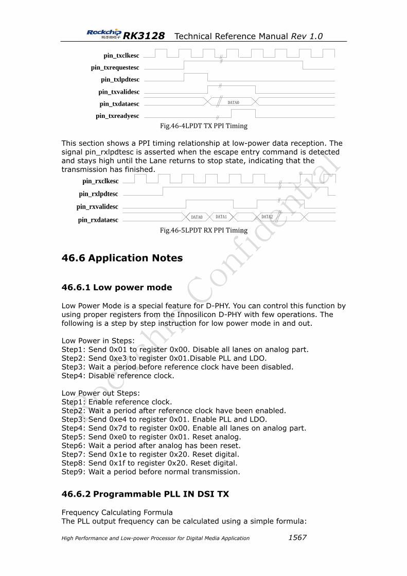
This section shows a PPI timing relationship at low-power data transmission
operation. The Protocol directs the Data Lane to enter Low-Power data transmission Escape mode by asserting pin_txrequestesc with pin_txlpdtesc
high. The Low-Power transmit data is transferred on the pin_txdataesc lines
when pin_txvalidesc and pin_txreadyesc are both active at a rising edge of
pin_txclkesc.
RK3128 Technical Reference Manual Rev 1.0
High Performance and Low-power Processor for Digital Media Application 1567
pin_txclkesc
pin_txrequestesc
DATA0
pin_txvalidesc
pin_txdataesc
pin_txreadyesc
pin_txlpdtesc
Fig.46-4LPDT TX PPI Timing
This section shows a PPI timing relationship at low-power data reception. The
signal pin_rxlpdtesc is asserted when the escape entry command is detected and stays high until the Lane returns to stop state, indicating that the
transmission has finished.
pin_rxclkesc
pin_rxlpdtesc
pin_rxvalidesc
pin_rxdataescDATA0 DATA1 DATA2
Fig.46-5LPDT RX PPI Timing
46.6 Application Notes
46.6.1 Low power mode
Low Power Mode is a special feature for D-PHY. You can control this function by
using proper registers from the Innosilicon D-PHY with few operations. The
following is a step by step instruction for low power mode in and out.
Low Power in Steps:
Step1: Send 0x01 to register 0x00. Disable all lanes on analog part.
Step2: Send 0xe3 to register 0x01.Disable PLL and LDO. Step3: Wait a period before reference clock have been disabled.
Step4: Disable reference clock.
Low Power out Steps:
Step1: Enable reference clock.
Step2: Wait a period after reference clock have been enabled. Step3: Send 0xe4 to register 0x01. Enable PLL and LDO.
Step4: Send 0x7d to register 0x00. Enable all lanes on analog part.
Step5: Send 0xe0 to register 0x01. Reset analog. Step6: Wait a period after analog has been reset.
Step7: Send 0x1e to register 0x20. Reset digital.
Step8: Send 0x1f to register 0x20. Reset digital. Step9: Wait a period before normal transmission.
46.6.2 Programmable PLL IN DSI TX
Frequency Calculating Formula
The PLL output frequency can be calculated using a simple formula:

RK3128 Technical Reference Manual Rev 1.0
High Performance and Low-power Processor for Digital Media Application 1568
PLL_Output_Frequency = FREF/PREDIV*FBDIV
PLL_Output_Frequency: It is equal to DDR- Clock-Frequency * 2
FREF :PLL input reference frequency which equals to the frequence of the pin_clkhtref
PREDIV : PLL input reference clock divider which can be configured by the
register of reg_prediv FBDIV :Integer value programmed into feedback divider which can be
configured by the register of reg_fbdiv
For example, FREF =20MHz, PLL output frequence = 800Hz, so set PREDIV=1, FBDIV=40
Additional Programming Considerations 1. The divided reference frequency (FREF/PREDIV) should be less than 40MHz.
2. The all possible settings of feedback divider are 12,13,14,16~511.
46.6.3 LVDS mode
Lvds source from LCDC0 or LCDC1.
Step1: configure lvds_format
8bit mode format-1 : GRF_LVDS_CON0[2:1]=0x00;
8bit mode format-2 : GRF_LVDS_CON0[2:1]=0x01; 8bit mode format-3 : GRF_LVDS_CON0[2:1]=0x10;
6bit mode : GRF_LVDS_CON0[2:1]=0x11;
MSB is on D0 : GRF_LVDS_CON0[3]=0x0;
MSB is on D7 : GRF_LVDS_CON0[3]=0x1;
Step3: configure MIPI-PHY
Configure PLL:
MIPIPHY_REG3=0x1; MIPIPHY_REG4=0x7;
Configure LVDS Interface:
MIPIPHY_REGE0=0x25; MIPIPHY_REGEA=0xf8;
Step4: enable lvds GRF_LVDS_CON0[6]=0x1;
46.6.4 Other mipi_phy grf
Other mipi_phy control registers description reference to GRF_LVDS_CON0.

RK3128 Technical Reference Manual Rev 1.0
High Performance and Low-power Processor for Digital Media Application 1569
46.7 ELECTRICAL SPECIFICATIONS
46.7.1 DC SPECIFICATIONS
Table 46-1 HS Transmitter DC specifications
Parameter Description Min Nom Max Unit Note
VCMTX
HS TX
staticCommon-mode
voltage
150 200 250 mV 1
|ΔVCMTX(1,0)
|
VCMTX mismatch when output is
Differential-1 or
Differential-0
5 mV 2
|VOD| HS transmit differential voltage
140 200 270 mV 1
|ΔVOD| VOD mismatch when output is
Differential-1 or
Differential-0
10
mV 2
VOHHS HS output high voltage
360 mV 1
ZOS Single ended output
impedance
40 50 62.5 ohm
ΔZOS Single ended output
impedance
mismatch
10 %
1. Value when driving into load impedance anywhere in the ZID range. 2. It is recommended the implementer minimize ∆VOD and ∆VCMTX(1,0) in
order to minimize radiation and optimize signal integrity.
Table 46-2 HS Transmitter DC specifications
Parameter Description Min Nom Max Unit Note
VIH Logic 1 input voltage 880 mV
VIL Logic 0 input voltage, not
in
ULPState
550 mV
VIL-ULPS Logic 0 input voltage, ULP State
300 mV
VHYST Input hysteresis 25 mV
Table 46-3 LP Transmitter DC Specifications
Parameter Description Min Nom Max Unit Note
VOH The venin output high
level
1.1 1.2 1.3 V
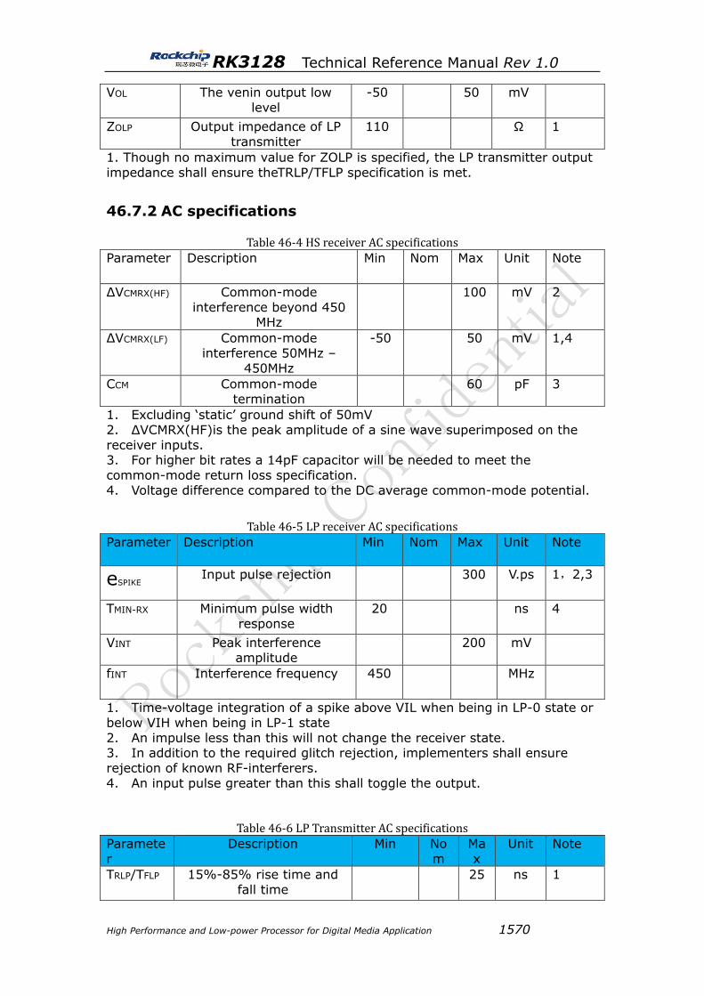
RK3128 Technical Reference Manual Rev 1.0
High Performance and Low-power Processor for Digital Media Application 1570
VOL The venin output low
level
-50 50 mV
ZOLP Output impedance of LP
transmitter
110 Ω 1
1. Though no maximum value for ZOLP is specified, the LP transmitter output
impedance shall ensure theTRLP/TFLP specification is met.
46.7.2 AC specifications
Table 46-4 HS receiver AC specifications
Parameter Description Min Nom Max Unit Note
ΔVCMRX(HF) Common-mode
interference beyond 450 MHz
100 mV 2
ΔVCMRX(LF) Common-mode
interference 50MHz –
450MHz
-50 50 mV 1,4
CCM Common-mode termination
60 pF 3
1. Excluding ‘static’ ground shift of 50mV
2. ΔVCMRX(HF)is the peak amplitude of a sine wave superimposed on the
receiver inputs. 3. For higher bit rates a 14pF capacitor will be needed to meet the
common-mode return loss specification.
4. Voltage difference compared to the DC average common-mode potential.
Table 46-5 LP receiver AC specifications
Parameter Description Min Nom Max Unit Note
eSPIKE Input pulse rejection 300 V.ps 1,2,3
TMIN-RX Minimum pulse width
response
20 ns 4
VINT Peak interference amplitude
200 mV
fINT Interference frequency 450 MHz
1. Time-voltage integration of a spike above VIL when being in LP-0 state or
below VIH when being in LP-1 state
2. An impulse less than this will not change the receiver state. 3. In addition to the required glitch rejection, implementers shall ensure
rejection of known RF-interferers.
4. An input pulse greater than this shall toggle the output.
Table 46-6 LP Transmitter AC specifications
Paramete
r
Description Min No
m
Ma
x
Unit Note
TRLP/TFLP 15%-85% rise time and
fall time
25 ns 1

RK3128 Technical Reference Manual Rev 1.0
High Performance and Low-power Processor for Digital Media Application 1571
TREOT
30%-85% rise time and
fall time
35 ns 1,5,6
TLP-PULSE-T
X Pulse width
of
exclusive-OR clock the
LP
First LP
exclusive-O
R clock pulse after
Stop state
or last pulse before Stop
state
40 ns
4
All other
pulses
20 4
TLP-PER-TX Period of the LP exclusive-OR
clock
90 ns
δV/δtSR Slew rate @ CLOAD = 0pF 500 mV/n
s
1,3,7,8
Slew rate @ CLOAD = 5pF 300 mV/n
s
1,3,7,8
Slew rate @ CLOAD = 20pF 250 mV/ns
1,3,7,8
Slew rate @ CLOAD = 70pF 150 mV/ns
1,3,7,8
Slew rate @ CLOAD = 0 to
70pF(Falling Edge Only)
30 mV/n
s
1,2,3
Slew rate @ CLOAD = 0 to
70pF(Rising Edge Only)
30 mV/n
s
1,3,9
Slew rate @ CLOAD = 0 to
70pF(Rising Edge Only)
30-0.07
5 * (VO,INST
– 700)
mV/n
s
1,10,1
1
CLOAD Load capacitance 0 70 pF 1
1. CLOAD includes the low-frequency equivalent transmission line capacitance.
The capacitance of TX and RX are assumed to always be <10pF. The distributed line capacitance can be up to 50pF for a transmission line with 2ns delay.
2. When the output voltage is between 400 mV and 930 mV.
3. Measured as average across any 50 mV segment of the output signal transition.
4. This parameter value can be lower than TLPX due to differences in rise vs.
fall signal slopes and trip levels and mismatches between Dp and Dn LP transmitters. Any LP exclusive-OR pulse observed during HS EoT (transition
from HS level to LP-11) is glitch behavior as described in section 8.2.2.
5. The rise-time of TREOT starts from the HS common-level at the moment the differential amplitude drops below 70mV, due to stopping the differential drive.
6. With an additional load capacitance CCM between 0 and 60pF on the
termination center tap at RX side of the Lane 7. This value represents a corner point in a piecewise linear curve.
8. When the output voltage is in the range specified by VPIN(absmax).
9. When the output voltage is between 400 mV and 700 mV.
10. Where VO,INSTis the instantaneous output voltage, VDP or VDN, in millivolts.

RK3128 Technical Reference Manual Rev 1.0
High Performance and Low-power Processor for Digital Media Application 1572
11. When the output voltage is between 700 mV and 930 mV.