chapter 4 transient photoconductivity decay …thesis.library.caltech.edu/3019/6/chapter4.pdf ·...
TRANSCRIPT

113
Chapter 4
Transient Photoconductivity Decay Measurements of Polymer-
Terminated Silicon Surfaces

114
1. Introduction
The fabrication of conducting and/or nonconducting organic overlayers on
crystalline Si surfaces is of interest for inhibiting of surface corrosion processes,1 for
providing routes to chemical control over the electrical properties of Schottky barrier-like
structures,2 for enabling novel lithographic strategies that utilize contact printing and
photopatterning,3-5 for producing novel metal-insulator-semiconductor devices,6 and for
controlling the electrical recombination properties of Si surfaces,7,8 amongst other
applications. To obtain acceptable electrical device properties, many of these
applications require direct functionalization of the Si surface in a fashion that does not
introduce significant densities of interfacial electronic defect levels. The presence of a
native oxide on Si is largely unacceptable for such purposes because the resulting Si/Si
oxide interface is often highly electrically defective.9,10 In addition, the oxide acts as a
tunneling barrier for charge carriers and the uniformity of this barrier is difficult to
control at the molecular level. Thermally grown silicon oxides generally contain fixed
positive charge,9,11-13 which also limits the types of electrical device behavior that can be
obtained from such interfaces. The ability to form electrically conductive or
nonconductive overlayers of controlled thickness on Si without relying on reactions that
utilize functionality arising from native and/or thermally grown Si oxides would be
important and desirable for future technological advancements.
Langmuir-Blodgett techniques14 have been used to synthesize organic thin films
with controlled structure and composition; however, the fragility of the resulting films
represents a major obstacle to practical implementation. Another method that has been
adopted for controlling the surface properties of a solid is by functionalizing the surface
with tethered polymer chains, called polymer brushes. Polymer brushes are polymers
confined to a small volume near an interface, and restrictions due to steric requirement

115
force the chains to stretch away from the grafting point to the edge of polymer layer.
Several strategies have been employed to prepare brush-type polymer layers, including
selective physisorption of block copolymers,15-17 chemical grafting of preformed polymer
chains onto the surface (�grafting to�),18-20 and �grafting from� methods that involve
surface-initiated polymerization.21-27 As adsorbed block copolymers face a disadvantage
of thermal instability, more robust films have been obtained using polymers with
functionalities appropriate for covalent attachment to surfaces. The significant
improvement in physical properties, however, generally is accompanied by a loss of
control over the order and composition of the overlayer. The �grafting to� approach also
produces polymer layers with low grafting density. Crowding of the chains at the surface
occurs as more polymers are grafted onto the substrate, which hinders the diffusion of
reactive chain ends to the surface for further grafting. The surface-initiated
polymerization can overcome this limitation by first attaching reactive units that are able
to initiate polymerization on the substrate, leaving the propagating polymer chains to
grow away from the surface. Since the smaller monomer can readily access the initiator
site at the end of propagating chain, the grafting density is greatly increased. Examples
of the �grafting from� method for Si surface modification include radical chain
polymerization initiated by surface-bound azo compounds,24 sequential cationic and atom
transfer radical polymerization,25 living free radical polymerization,27 polymerization by
organometallic initiators,26 and ring-opening metathesis polymerization.21 However, all
these polymerization techniques utilize the reactions between chlorosilane moieties and
silicon oxide surfaces, and result in an intervening Si oxide layer between the Si and
surface functionality (see Figure 4.1). In order to prepare polymer-modified Si surfaces
that are suitable for electronic device applications, a method was developed for the
formation of an organic overlayer directly on the Si substrate through a covalent Si-C
linkage.

116
Crystalline Si has recently been functionalized using a variety of approaches;28-42
notably, alkylation of crystalline, (111)-oriented Si using a two-step
chlorination/alkylation procedure can produce functionalized surfaces that have a very
low surface recombination velocity.8,43 This modification method was developed and
thoroughly characterized by Ashish Bansal, and was crucial for the work of this chapter.
The work described in this chapter was also inspired in part by a prior study of Weck et
al., who first showed the possibility of producing surface-immobilized polymer brushes
using surface-initiated ring-opening metathesis polymerization (ROMP). They reported
the polymerization of substituted norbornenes from a modified gold surface using a Ru-
based alkylidine as initiator, though only small amounts of polymer chains were
formed.44 This chapter describes the extension of chlorination/alkylation chemistry,
combined with ROMP methods, to produce polymer overlayers that are covalently
attached directly to a Si(111) surface and provide molecular-level control over the
thickness and electronic properties of the resulting Si/polymer contacts.

117
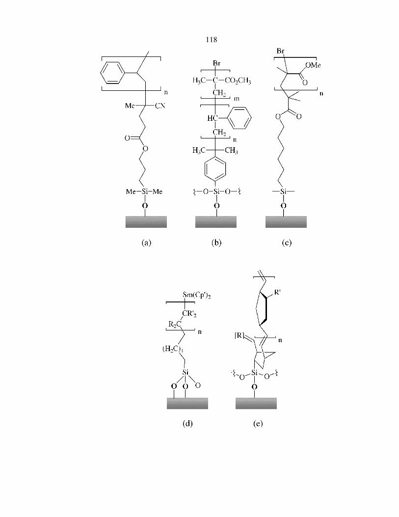
Figure 4.1
Examples of polymer-terminated Si reported in literature utilizing �graft from� approach
to form covalently attached polymers or block copolymers on Si surfaces. The surface-
initiated polymerization method includes (a) radical chain polymerization initiated by
surface-bound azo compounds,24 (b) sequential cationic and atom transfer radical
polymerization,25 (c) living free radical polymerization,27 (d) polymerization by
organometallic initiators,26 and (e) ring-opening metathesis polymerization.21 All above
methods relied on chlorosilane chemistry to link the polymer layer to the SiO2 substrate,
and resulted in an intervening oxide layer which can be unsuitable for electronic device
applications that require a low surface defect density.
118

119
2. Experimental
2.1. Chemicals
All solvents used for surface modification, including acetonitrile, chlorobenzene,
1,2-dichloroethane, dichloromethane, methanol, and tetrahydrofuran (THF), were
purchased from Aldrich or Acro in the anhydrous form and used as received. Solvents
were stored over activated 3 Å molecular sieves (EM Science) in an N2(g)-purged glove
box. Solvents used for wafer degreasing, acetone, dichloromethane, methanol, and 1,1,1-
trichloroethane, were either reagent grade (GR) or Omnisolve grade obtained from EM
Science and used as received. Hydrogen peroxide (30%) was purchased from EM
Science, and H2SO4(aq) was obtained from J.T. Baker. Hydrofluoric acid buffered with
ammonium fluoride (NH4F/HF, buffered HF) and 40% ammonium fluoride (NH4F)
solutions were purchased from Transene Co. Phosphorus pentachloride (PCl5), benzoyl
peroxide, allylmagnesium chloride (CH2=CHCH2MgCl, 1.0 M in THF) were obtained
from Aldrich and were used without further purification. The ring-opening metathesis
catalyst [RuCl2(=CHPh)(PCy3)2, Cy = cyclohexyl] (1) was obtained from Materia while
[RuCl2(=CHPh)(PCy3)(IMesH2), IMes = dimesityl-imidazolidene] (2) was provided by O.
A. Scherman.45 Monomers norbornene (Aldrich) and dicyclopentadiene (DCPD,
Materia) were dissolved in anhydrous 1,2-dichloroethane and anhydrous
dichloromethane, respectively. 1,3,5,7-Cyclooctatetraene (COT) was obtained from
BASF and dried over CaH2, while 1,5-Cyclooctadiene (COD) was purchased from
Aldrich. Both COD and COT were distilled before used. C5, C4, and C6 olefin Grignard
reagents, 4-pentenylmagnesiumbromide (CH2=CH(CH2)3MgBr, ~1.0 M in THF), 3-
butenylmagnesiumbromide (CH2=CH(CH2)3MgBr, ~1.5 M in THF) and the 5-

120
hexenylmagnesiumbromide (CH2=CH(CH2)4MgBr, ~1.0 M in THF), were provided by O.
A. Scherman.
2.2. Preparation of Substrates
Single-crystal, (111)-oriented, n-type float-zone silicon wafers were obtained
from Topsil Semiconductor Materials. The double-side polished wafers were 280 ± 20
µm thick, and phosphorous-doped with resistivities of 3500�6500 W·cm as specified by
the manufacturer. The bulk lifetime of 6760 µs was measured by the photoconductive
decay method at the manufacture. The silicon wafers were first oxidized in a �Pirhana�
solution which consisted of 3:1 (v/v) concentrated H2SO4(aq):H2O2 (30%) heated to
approximately 100 ∞C for one hour.33 Caution: The acidic “Pirhana” solution is
extremely dangerous, particularly in contact with organic materials and should be
handled carefully. The wafers were then rinsed with copious amount of 18.0 MW◊cm
resistivity water (obtained from a Barnstead Inc. Nanopure water purification system),
dried under pressurized N2(g), and stored for future use. Before surface modifications,
the wafer was cut into approximately 9 mm ¥ 9 mm size samples. Each piece was briefly
sonicated in 18.0 MW◊cm resistivity water, degreased by rinsing sequentially with
methanol, acetone, 1,1,1-trichloroethane, dichloromethane, 1,1,1-trichloroethane,
acetone, and methanol, and followed by another brief sonication in water. After blow
drying with N2(g), the samples were etched in NH4F/HF (buffered HF) for 30 seconds,
and then directly immersed in 40% NH4F for 15�20 min.46 Following the etching
process, the samples were rinsed with 18.0 MW◊cm resistive water (obtained from
Barnstead E-pure filtration system), and dried under a stream of N2(g). The samples were
quickly mounted onto the XPS stubs and introduced into ultrahigh vacuum (UHV)
system that houses the x-ray photoelectron spectroscopy (XPS) via an atmospheric load
lock for immediate surface characterization.

121
2.3. Surface Modification
All surface modification procedures were carried out in an N2(g)-purged glove
box which is connected to the UHV system housing the XPS spectrometer via a gate
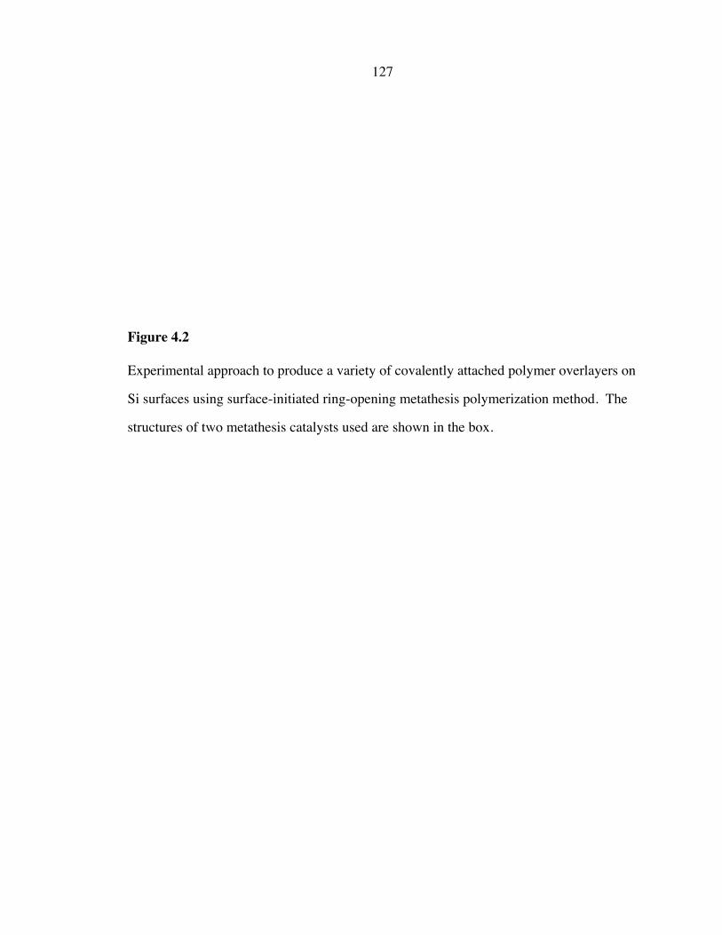
valve. Figure 4.2 depicts the schematic experimental approach: (i) an alkenyl linker of
variable length is coupled to a chlorinated Si surface using a Grignard reaction; (ii) an
olefin cross-metathesis reaction is used to obtain a surface-bound ruthenium ring-opening
metathesis polymerization (ROMP) catalyst layer, and (iii) a monomer is added to effect
growth of polymer onto the surface.
2.3.1. Chlorination
After verifying that the etching process was successful as determined by the
absence of oxide on the Si surfaces, the samples were brought into the N2(g)-purged
glove box directly through the gate valve. The stock chlorinating solution was prepared
by dissolving excess PCl5 in chlorobenzene to form a saturated solution (typically 0.6�0.7
M). The solution was warmed to about 60 ∞C for at least 1 hour to dissolve as much PCl5
as possible. Immediately before use, a small portion of the stock chlorinating solution
was poured into a small beaker, and a few grains of benzoyl peroxide were added
(approximately 30�40 mg of benzoyl peroxide in 10 ml of PCl5-chlorobenzene solution)
as a radical initiator.47,48 With the samples completely immersed in this solution and the
beaker covered by a watch glass, the reaction was heated to 90�100 ∞C for 45�60 min.
The samples were then taken out of the chlorinating solution, rinsed with anhydrous THF
followed by anhydrous methanol or anhydrous dichloromethane, and dried in a stream of
N2(g). Some samples were mounted on the XPS stub and brought into the UHV system
for surface characterization.

122
2.3.2. Terminal-Olefin Addition via Grignard Reaction
The chlorinated Si samples were placed in separate test tubes so that Si pieces
were in standing position and the surfaces did not touch the bottom of reaction vessels.
The olefin Grignard reagent was then added to each test tube and heated to 65�80 ∞C for
8�18 hours. The reaction time varied according to the chain length of the terminal olefin
group (see Table 4.1). Two procedures requiring different types of test tubes and rinsing
solvents were adapted depending on the Grignard reagent used. When allylmagnesium
chloride (Aldrich) or C4 olefin Grignard was used, the reaction took place in test tubes
capped with septa. Following the overnight reaction, the samples were rinsed with
copious amount of anhydrous THF and anhydrous methanol, individually immersed in
anhydrous methanol in screw-capped vials, and taken out of the glove box for sonication.
The derivatized samples were sonicated in anhydrous methanol and anhydrous
acetonitrile for 5 min each, dried in a stream of N2(g) before being mounted on the XPS
stub, and introduced into UHV through atmospheric load lock for surface
characterization.
Due to a longer reaction time when C5 or C6 olefin Grignard was used, it was
necessary to eliminate as much methanol vapor in the glove box as possible. Prior to the
reaction, fresh phosphorous pentaoxide (P2O5) powders were poured into an evaporation
dish and used as a drying agent to absorb solvent vapors in the glove box. Anhydrous
dichloromethane was used in place of anhydrous methanol throughout the surface
modification procedures. The samples were immersed in anhydrous dichloromethane
when taken out of the glove box and sonicated in anhydrous dichloromethane, anhydrous
methanol, and anhydrous acetonitrile for 5 min each. During the reaction, the samples
were also isolated from the glove box atmosphere by using teflon-lined screw-capped test
tubes instead of septa-capped ones. For each experiment, only a fresh portion of
homemade Grignard reagent was brought into the glove box in a Schlenk tube, and the
123
portion was defrosted by warming to ~45 ∞C immediately before use. Allylmagnesium
chloride bottle was stored in the glove box for no more than one month, and the solution
was drawn with a syringe through the Sure/Seal cap.
2.3.3. Catalyst Addition
Olefin-terminated-Si samples were placed into several screw-capped vials
containing a ruthenium-alkylidine ring-opening metathesis catalyst solution for at least 3
hours. Then the samples were washed copiously with anhydrous dichloromethane and
dried with a stream of N2(g). The ruthenium catalyst solution was made immediately
prior to use by dissolving Cl2(Cy3P)2Ru=CHPh (1, ~25 mM) in anhydrous
dichloromethane. A more powerful catalyst Cl2(H2IMes)(PCy3)Ru=CHPh (2, ~10 mM in
anhydrous dichloromethane) was also used for some experiments involving polymerizing
cyclooctatetraene (COT) and norbornene.
2.3.4. Polymerization
The stock norbornene solution (2.44 M) was made by dissolving norbornene in
anhydrous 1,2-dichloroethane and stored in a Schlenk tube covered with an aluminum
foil. In screw-capped vials, less concentrated norbornene solutions (0.01 M, 0.05 M, 0.09
M, 0.15 M, 0.18 M, 0.27 M, and 0.45 M) were made from the stock prior to catalyst
addition reaction. This is to minimize the exposure of the stock solution to any
ruthenium catalyst in the glove box atmosphere. Small vials that allow only the edges of
a sample to touch the vial wall and the bottom were used. The desired monomer solution
was then added into the vials and the vials were capped quickly. The standard reaction
time for norbornene, COD, and COT was 30 min at room temperature, and then washed
with copious amount of anhydrous dichloromethane and dried in a stream of N2(g). The
dicyclopentadiene (DCPD) polymerization was carried out by first immersing the
samples in a DCPD solution (2.5 M in dichloromethane) for 30 min at room temperature.
124
Then the DCPD solution was drained, and the vials and samples were washed with
anhydrous dichloromethane. A fresh portion of anhydrous dichloromethane was added
into the vials, and the samples were then heated to ~40�50 ∞C for 5�10 min to allow
cross-linking of attached polymer. Samples were washed and dried the same way.
At least one sample per batch was characterized by XPS, and these samples were
not used in the photoconductivity decay measurements. The XPS samples were mounted
onto the stub and transferred into the glove box load lock through the gate valve, while
samples for the photoconductivity decay measurements were placed separately in the
open glass vessels and pumped in the antichamber of the glove box for at least 3 hours.
Before performing the photoconductivity decay measurements, samples were taken into
the glove box and sealed in glass vessels under N2(g), and then brought out of the glove
box for measurements. For overlayer thickness measurements and scanning electron
microscopy, samples were mounted onto the XPS stub, characterized by XPS, and then
taken out through the atmospheric load lock.
2.4. Surface Characterizations
2.4.1. X-ray Photoelectron Spectroscopy
The XPS experiments were conducted in an M-probe surface spectrometer (VG
Instrument) pumped by a CTI Cryogenics-8 cryo pump. Samples could be introduced
into the UHV system using either the atmospheric load lock or the glove box load lock.
The atmospheric load lock was pumped by a Varian model V80 turbo pump and a Varian
model SD-300 mechanical pump, and allowed samples to be introduced into the UHV
from air. The glove box load lock was pumped by a Varian model V200 turbo pump and
a Varian model SD-300 mechanical pump, and enabled samples to be transferred into the
UHV through a gate valve that opened to the N2(g)-purged glove box. These load locks

125
were brought to the atmospheric pressure by back-filling with N2(g), and can be pumped
down to approximately 10�7 Torr in about 10 min. Samples were mounted on a stainless
steel or aluminum stub with screws.
The XPS chamber was maintained at a base pressure of less than 5 ¥ 10�10 Torr,
although the operating pressure was 5 ¥ 10�9 to 2 ¥ 10�8 Torr. Monochromatic Al Ka x-
rays (hv = 1486.6 eV) incident at 35° from the sample surface were used to excite
electrons from the sample, while the emitted electrons were collected by a hemispherical
analyzer at a take-off angle of 35∞ from the plane of the sample surface. Data collection
and analysis were done with the M-probe package software version 3.4. Survey scans
were collected in the scanned mode with an elliptical spot of dimensions 800 µm ¥ 1200
µm incident on the sample surface. The high-resolution scans were recorded in an
unscanned mode with the same spot size. A typical XPS characterization of a surface
consisted of one survey scan from 0�700 eV binding energies and a high resolution scan
of the Si 2p region (97.57�104.59 eV binding energies). In certain cases when Si 2p peak
was very small or undetected, the high-resolution scan was omitted.
2.4.2. Overlayer Thickness Measurements: Ellipsometry and Profilometry
The thicknesses of polymer overlayers formed using different concentrations of
norbornene and DCPD were measured by either ellipsometry or profilometry.
Ellipsometric measurements were performed on a Gaertner variable angle ellipsometer
model L116C using a helium-neon laser (l = 632.8 nm) and a 45∞ polarizer, with an
incident angle set to 70∞. The film thickness was calculated using the software package
provided by Gaertner. The index of refraction NS and the absorption coefficient KS of the
substrate were determined using a freshly etched Si, and these numbers were used as
standards when film thicknesses were measured. An indexes of refraction NF = 1.46 was
used for both terminal olefin and polymer layers. Film thickness was measured at six
126
different locations on each sample, and two measurements were done at each spot. The
measured thickness values for all samples were ±1 Å for a particular spot.
Profilometric measurements of several polynorbornene-terminated Si samples
polymerized from 0.15M, 0.45 M, and 2.44 M norbornene solution were performed using
Sloan Dektak 3030 surface profiling measuring system with a diamond stylus (12.5 µm
radius). The stylus force was set to 10 mN, and with the speed set to low, scan length of
4 mm was selected for most measurements. A stainless steel spatula was used to scrape
away a thin stripe of the polynorbornene overlayer, and the profile of the surface features
was plotted. By measuring the depth of the scribe, the thickness of the polymer was
determined.
2.4.3. Scanning Electron Microscopy
Images of polynorbornene overlayers and sample cross section were obtained
using Camscan series II scanning electron microscope (SEM). It was equipped with an
Everhart-Thornley secondary-electron imaging, a Robinson-type backscattered electron
detector for atomic-number-contrast imaging, and a relatively slow speed absorbed
current imaging system. An on-board frame averaging system was used to integrate
several scan frames in order to reduce noise, and the working resolution of the Camscan
was approximately 100 nm. Digital imaging was performed using the 4Pi Systems
Scanning Interface Unit for digital beam control, and images were acquired under an
operating pressure of 10�5 Torr. The acquired digital images were stored in a computer
and processed off-line using NIH Image program. Samples with different
polynorbornene overlayer thicknesses were prepared using 0.15 M, 0.45 M, and 2.44 M
norbornene solutions. The surface uniformity of the polymer layers was examined under
a 500¥ magnification. A cross-sectional SEM image of a sample prepared using 2.44 M
norbornene/1,2-dichloroethane solution was also obtained under a 1500¥ magnification
and the polymer thickness was estimated from the image.
127
Figure 4.2
Experimental approach to produce a variety of covalently attached polymer overlayers on
Si surfaces using surface-initiated ring-opening metathesis polymerization method. The
structures of two metathesis catalysts used are shown in the box.

128

129
Table 4.1
List of reagents and reaction conditions used for each step of the Si surface modification
procedure.
Reaction Reagents Reaction Time Reaction Temperature
Chlorination PCl5 in chlorobenzene + benzoyl peroxide
45 � 60 min 90 � 100 ûC
8 � 15 hr 65 � 80 ûC
8 � 15 hr 65 � 80 ûC
14 � 18 hr 65 � 80 ûC
16 � 18 hr 65 � 80 ûC
Catalyst Additionb Ru complex 1 3 hr Room Temp.
Ru complex 2 3 hr Room Temp.
Polymerization Norbornene in 1,2-dichloroethane 30 min Room Temp.
(1) DCPD in dichloromethane
30 min Room Temp.
(2) Heat treatment in dichloromethane 5 min 40 � 50 ûC
Terminal Olefin Additiona
a The solvent used for this reaction was THF, and the approximate Grignard reagent concnetrations were 1�1.5 M.b The solvent used to dissolve Ru complexes was anhydrous dichloromethane.
MgCl
MgBrMgBr
MgBr
130
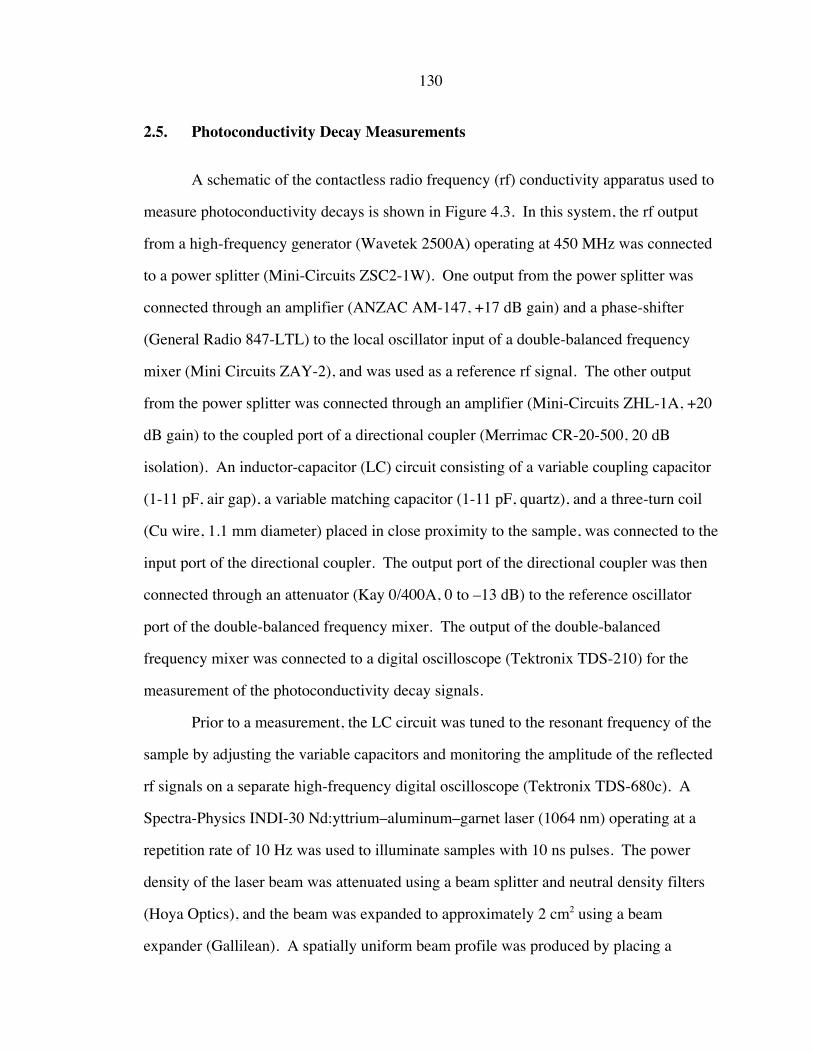
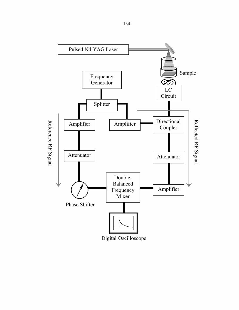
2.5. Photoconductivity Decay Measurements
A schematic of the contactless radio frequency (rf) conductivity apparatus used to
measure photoconductivity decays is shown in Figure 4.3. In this system, the rf output
from a high-frequency generator (Wavetek 2500A) operating at 450 MHz was connected
to a power splitter (Mini-Circuits ZSC2-1W). One output from the power splitter was
connected through an amplifier (ANZAC AM-147, +17 dB gain) and a phase-shifter
(General Radio 847-LTL) to the local oscillator input of a double-balanced frequency
mixer (Mini Circuits ZAY-2), and was used as a reference rf signal. The other output
from the power splitter was connected through an amplifier (Mini-Circuits ZHL-1A, +20
dB gain) to the coupled port of a directional coupler (Merrimac CR-20-500, 20 dB
isolation). An inductor-capacitor (LC) circuit consisting of a variable coupling capacitor
(1-11 pF, air gap), a variable matching capacitor (1-11 pF, quartz), and a three-turn coil
(Cu wire, 1.1 mm diameter) placed in close proximity to the sample, was connected to the
input port of the directional coupler. The output port of the directional coupler was then
connected through an attenuator (Kay 0/400A, 0 to �13 dB) to the reference oscillator
port of the double-balanced frequency mixer. The output of the double-balanced
frequency mixer was connected to a digital oscilloscope (Tektronix TDS-210) for the
measurement of the photoconductivity decay signals.
Prior to a measurement, the LC circuit was tuned to the resonant frequency of the
sample by adjusting the variable capacitors and monitoring the amplitude of the reflected
rf signals on a separate high-frequency digital oscilloscope (Tektronix TDS-680c). A
Spectra-Physics INDI-30 Nd:yttrium�aluminum�garnet laser (1064 nm) operating at a
repetition rate of 10 Hz was used to illuminate samples with 10 ns pulses. The power
density of the laser beam was attenuated using a beam splitter and neutral density filters
(Hoya Optics), and the beam was expanded to approximately 2 cm2 using a beam
expander (Gallilean). A spatially uniform beam profile was produced by placing a

131
holographic diffuser (Coherent, 1°) directly above the sample. The measurements were
obtained under high-level injection conditions by adjusting the power density of the
expanded incident beam to ~1 ¥ 10�3 mJ pulse�1 using neutral density filters. The incident
beam power was determined using a power meter (Coherent Fieldmaster GS) equipped
with a pyroeletric sensor (Coherent LM-P10i). The intensity of the light pulse at high-
level injection was sufficient to eliminate equilibrium potential drop that might exist in
the solid. Therefore imply that the changes in the observe carrier recombination lifetime
are primarily due to changes in surface state density and/or the carrier-capture rate
constants by surface traps. The sample was placed in a seal glass vessel which allows the
sample to be in contact with either air or N2(g) during the period of measurement. Time
constants were obtained by fitting the average of 128 decays to a single exponential and
averaging over a minimum of three samples for each type of surface and storage
condition.
Time-resolved photoconductivity decays of six types of surfaces stored in a
controlled environment at 21 ∞C and 7% relative humidity (R.H.) were recorded. In
addition, three types of surfaces were subjected to a harsher environment at 40 ∞C and
80�90% R.H., and the effects on the photoconductivity decays were studied over a period
of one month. The initial measurement for each type of surface was performed
immediately after samples, sealed in the glass vessels under N2(g), were taken out of the
glove box. Then the glass vessels were opened to the air and the samples were stored
under one of the two controlled environmental conditions.
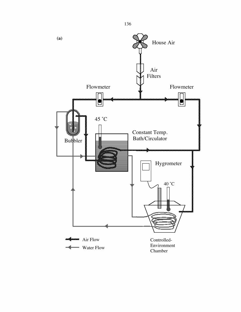
The 21 °C/7% R.H. environmental chamber was made by feeding a constant flow
of house air into a desiccator cabinet. An in-line oil-removal coalescing filter (Parker) in
conjunction with a microalescer filter (Wilkerson) was used to remove oil droplets and
vapor from the house air. Figure 4.4 displays the setup of the 40 °C/80�90% R.H.
environmental chamber. The filtered house air was first split into two paths, and two
Bel-Art Riteflow flowmeters were used to control the amount of air going through each

132
path. One path directed the air through a custom-made bubbler filled with deionized
water (kept at ~45 ∞C) to allow saturation of water vapor, and then passed through a heat-
exchange Cu coil immersed in a 45 ∞C constant-temperature bath/circulator (National
Instrument Type SCI). The warmed water-vapor-saturated air was then combined with
dry house air from the other path to create 80�90% R.H. and was introduced into a
insulated chamber where the samples were stored. The warm water in the constant-
temperature bath/circulator was also circulated through the outside jacket of the bubbler,
and another heat-exchange Cu coil inside the insulated chamber designed to keep the air
temperature at 40 ∞C. Samples were placed in separate test tubes while being stored in
the 40 ∞C/80�90% R.H. chamber, and in plastic dishes if stored in the 21 ∞C/7% R.H.
chamber. The relative humidity of each chamber was measured by a hygrometer
(Control Company).
133
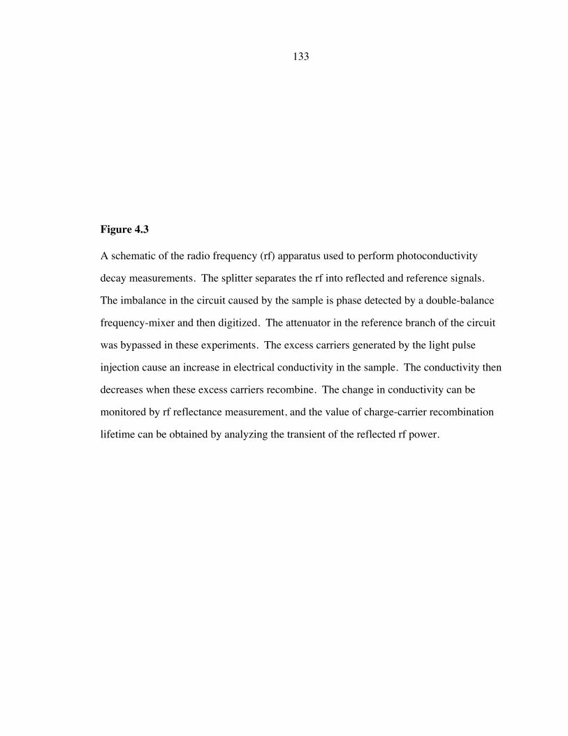
Figure 4.3
A schematic of the radio frequency (rf) apparatus used to perform photoconductivity
decay measurements. The splitter separates the rf into reflected and reference signals.
The imbalance in the circuit caused by the sample is phase detected by a double-balance
frequency-mixer and then digitized. The attenuator in the reference branch of the circuit
was bypassed in these experiments. The excess carriers generated by the light pulse
injection cause an increase in electrical conductivity in the sample. The conductivity then
decreases when these excess carriers recombine. The change in conductivity can be
monitored by rf reflectance measurement, and the value of charge-carrier recombination
lifetime can be obtained by analyzing the transient of the reflected rf power.
134
Digital Oscilloscope
DirectionalCoupler
Amplifier
Attenuator
Phase Shifter
Double-Balanced
FrequencyMixer
Reference R
F Signal
Reflected R
F Signal
S
FrequencyGenerator
Splitter
Attenuator
Amplifier
LCCircuit
Amplifier
Sample
Pulsed Nd:YAG Laser

135
Figure 4.4
(a) A schematic of the controlled-environment chamber for sample storage under an
elevated temperature and relative humidity condition. Filtered house air is split into two
paths; one path is designed to saturate the air with water vapor at 45 ∞C, and the other
path delivers original dry filtered house air. With the aid of flowmeters, two paths were
then combined to create an environment with an air temperature of 40 ∞C and 80�90%
relative humidity. (b) A photograph of the controlled-environment setup. (c) A detailed
photograph showing the interior of the chamber. The 45 ∞C water was circulated through
the Cu tubing to provide heating inside the chamber. The test tubes were used to hold the
samples being stored.
136
House Air
Hygrometer
Flowmeter
Controlled-EnvironmentChamber
Constant Temp.Bath/Circulator
Flowmeter
AirFilters
Air Flow
Water Flow
45 ûC
40 ûC
(a)
Bubbler

137
(b)
(c)
Chamber
Circulator
Bubbler
Filter
HygrometerFlowmeters
Test Tubes
Cu Coil

138
3. Results
3.1. Surface Modifications
Four monomers were used for the modification of Si(111) surfaces using ring-
opening metathesis polymerization (ROMP) method. The x-ray photoelectron
spectroscopy (XPS) results suggest that both norbornene and dicyclopentadiene (DCPD)
were successfully polymerized on the Si surfaces, but surface-initiated ROMP did not
produce detectable polymer overlayers with either cyclooctadiene (COD) or
cyclooctatetraene (COT) monomer.
The surface modification process was monitored and verified using XPS. Figure
4.5 displays the XP spectra obtained at each step of the surface modification process. A
successful etching procedure produces an H-terminated Si surface with a clean spectrum
showing large Si 2p and Si 2s peaks at 99 eV and 149 eV binding energies. The smaller
peaks present at successive intervals of 17.5 eV binding energy higher than the main Si
2p and 2s peaks were plasmon loss peaks, and were characteristic of Si surfaces.49,50
Small signals due to adventitious carbon and oxygen were often observed at 284.6 eV
(C 1s) and 532 eV (O 1s). The presence of adventitious carbonaceous material on the
silicon surface was a result of wet chemical etching and subsequent brief handling of
samples in air.51,52 The lack of signal in the 101 to 104 eV region of the Si 2p high-
resolution XP spectra collected with each survey scans suggested that the oxygen signal
observed in survey spectra was not due to silicon oxide.
Figure 4.5b shows the representative spectrum of a chlorinated Si surface.
Addition peaks were observed at 270 eV and 200 eV binding energies, which correspond
to Cl 2s and Cl 2p peaks.43 Attachment of the terminal olefin was confirmed by the
disappearance of the Cl peaks and the concomitant increase in magnitude of the C 1s

139
peak in the XP survey spectrum (Figure 4.5c). However, a direct evidence of the
attachment of Ru catalyst could not be confirmed using XPS data (Figure 4.5d). The
subsequent growth of polymer film and a set of control experiments offered indirect but
convincing confirmations of the catalyst addition reaction.
3.1.1. Polynorbornene-Terminated Si
For most polynorbornene films, growth of polymer was evidenced by the
disappearance of the Si signals and the formation of an overlayer that only displayed C
peaks in the XP survey scan (Figure 4.5e). When a low concentration (<0.09 M)
norbornene solution was used for polymerization, the observed survey spectrum
displayed an increase in magnitude of the C 1s peak while the magnitude of the Si peaks
were decreased but still visible. The surfaces of polynorbornene-terminated Si made with
higher concentration (2.44 M) norbornene solutions appeared colorful and the films were
thick enough to be visible by the naked eyes. Both C3 olefin- and C5 olefin-
polynorbornene-terminated Si surfaces were successfully made.
3.1.2. PolyDCPD-Terminated Si
The ROMP of DCPD was monitored using XPS in the same fashion as described.
Figure 4.6 displays the XPS survey spectra of polyDCPD-terminated Si surfaces made
from four different DCPD concentrations (0.27 M, 0.45 M, 0.98 M, and 2.5 M in
dichloromethane). The ROMP of DCPD did not produce polymer films of the same
thickness as seen with norbornene. Although the ring-strains of norbornenes and DCPDs
are very similar, the larger size of a DCPD monomer unit could hinder monomer
diffusion to the surface-bound Ru initiator and thus limit the film thickness. However,
the film thickness could still be controlled by the monomer concentrations as evidenced
by XPS analysis. When polymerized DCPD is subject to heat (~40�50 ûC) the remaining
cyclic olefins are expected to undergo ring-opening polymerization and cross-link with

140
neighboring olefins. Although the cross-linking property of polyDCPD on surfaces was
not investigated in this work, considering that the surface-bound polyDCPD chains are
immobilized, the extent of cross-linkage could be somewhat limited.
3.1.3. ROMP of COD and COT
Attempts to produce polyCOD- and polyCOT (polyacetylene)-terminated surfaces
were unsuccessful. The XP spectra showed no polymer formation on the Si surfaces
following either immersion of 1-modified Si into COD or immersion of 2-modified Si
into COT. Since COT is less strained than norbornene and COD, a more powerful Ru
catalyst 2 was used in place of 1 to initiate the ROMP reaction. The XP survey spectrum
shows no significant increase in the magnitude of C 1s peak. To be certain that the
catalyst 2 would initiate ROMP on a surface in a similar fashion as the catalyst 1, it was
used to polymerize norbornene (2.44 M in 1,2-dichloroethane). The resulting XP
spectrum revealed a large C 1s peak and no detectable Si peaks, and a colorful film was
seen on the surface as observed when norbornene was polymerized using catalyst 1.
Thus, surface bound 2 was successful at polymerize norbornene.
3.1.4. Control Experiments
Additional experiments were performed to establish that (i) the polymerization of
norbornene was directly initiated by 1, and (ii) the resulting polymer film was attached
covalently to the Si surface. When an olefin-terminated Si substrate was exposed to a
solution of norbornene, no polymer was observed by XPS (Figure 4.7a). In addition,
when an H-terminated Si surface was exposed to a solution of norbornene, no polymer
formed and the XPS signals showed only Si and a very small amount of adventitious C
and O (Figure 4.7b). Exposure of an H-terminated Si surface to a solution of 1 followed
by exposure to a solution of norbornene produced a polymer that did not persist on the Si
surface after washing with dichloromethane (Figure 4.7c). These wet chemical

141
experiments imply that the technique described in this chapter did in fact produce
covalently attached polymeric films on the Si surface, and the polymerization could not
occur without the Ru initiators.

142
Figure 4.5
XP survey spectra of (a) H-terminated Si, (b) Cl-terminated Si, (c) allyl-terminated Si, (d)
allyl-terminated Si after immersing in a solution of 1 for 3 hours, and (e) covalently
attached polynorbornene on Si. Spectra in (a)�(d) were normalized relative to the
intensity of the Si 2p peak. Typical Si 2p:C 1s:O 1s peak ratios were (a) 1:(0.35 ±
0.06):(0.36 ± 0.09), (b) 1:(0.54 ± 0.03):(0.39 ± 0.04) (average of 2 spectra), (c) 1:(0.82 ±
0.22):(0.68 ± 0.22), and (d) 1:(2.04 ± 0.26):(0.46 ± 0.12) (average of 2 spectra).

143
0100200300400500600700
Inte
nsit
y (a
.u.)
Binding Energy (eV)
Si 2pSi 2s
C 1sO 1s
(a)
(b)
(d)
(c)
(e)
Cl 2p
Cl 2s

144
Figure 4.6
XP survey spectra of polyDCPD-terminated Si made from solutions of (a) 0.27 M, (b)
0.45 M, (c) 0.98 M, and (d) 2.5 M DCPD in dichloromethane. All spectra were
normalized relative to the intensity of the Si 2p peak.

145
0100200300400500600700
Inte
nsit
y (a
.u.)
Binding Energy (eV)
Si 2p
Si 2s
C 1s
O 1s
(a)
(b)
(d)
(c)

146
Figure 4.7
XP survey spectra of (a) C4 olefin-terminated Si following immersion in norbornene
(2.44 M in 1,2-dichloroethane) for 30 min, (b) H-terminated Si following immersion in
the same norbornene solution for 30 min, and (c) H-terminated Si after being immersed
in a solution of 1 and then norbornene. All surfaces were rinsed with anhydrous
dichloromethane after each immersion. All spectra were normalized relative to the
intensity of the Si 2p peak. Compare to the spectrum of a polynorbornene-terminated Si
(Figure 4.5e), spectra (a)�(c) indicated no significant polymer growth after these surface
treatments.

147
0100200300400500600700
Inte
nsit
y (a
.u.)
Binding Energy (eV)
Si 2pSi 2s
C 1s
O 1s
(a)
(b)
(c)

148
3.2. Surface Characterizations
3.2.1. Polymer Thickness Measurements
Because ROMP initiated by 1 is a controlled polymerization process,53,54 different
film thicknesses could be obtained by varying the concentration of monomer solutions.
Table 4.2 summarizes the thicknesses of several polynorbornene films produced at a
fixed reaction time (30 min) in response to variation in the concentration of monomer in
the solution. The standard deviation in the ellipsometrically derived thickness measured
at several different spots for each sample was usually less than ±10% of the mean
thickness value, indicating that the polymer film covered the entire Si substrate. Figure
4.8a displays a partial surface profile of a polynorbornene-terminated Si made from a
2.44 M norbornene solution. This profile includes a feature representing the area of a
spatula scrape as shown in the SEM image of the same sample (see Figure 4.8b). The
upward spikes at the edges of the feature are most likely the result of polymer being
pushed and piled up to the sides when the spatula was used to scraped off small amount
of polymer on the surface. The center parts of these features are very flat and smooth,
which is a good indication of that being the flat surface of a Si substrate. The measured
profilometric thicknesses of both 0.15 M and 0.45 M polynorbornene films were
consistent with the ellipsometric data (Table 4.2). The polymer films formed using a
2.44 M solution were too thick for ellipsometric measurements, therefore only the
profilometric result is reported.
3.2.2. Scanning Electron Microscopy
Figure 4.9 shows two top-view images of polynorbornene-terminated Si samples
([norbornene] = 0.15 M and 2.44 M) at 500¥ magnification. A thinner polynorbornene
overlayer appears to be smoother compared to a thicker overlayer at the same
149
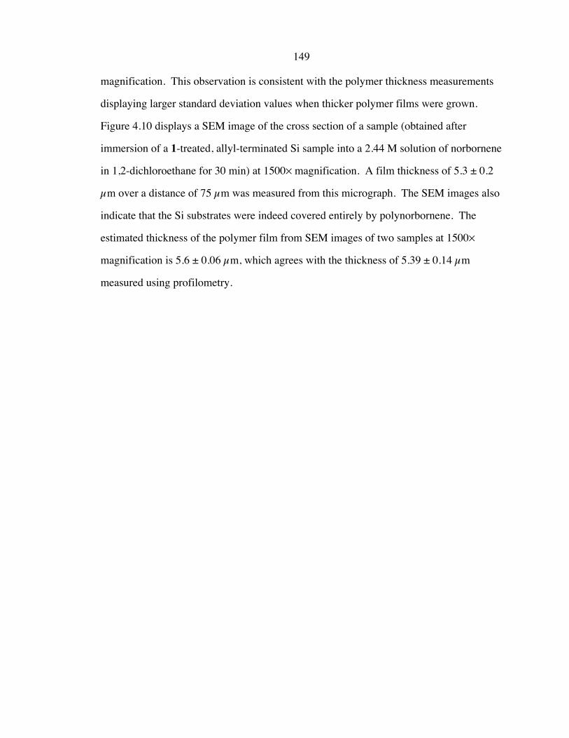
magnification. This observation is consistent with the polymer thickness measurements
displaying larger standard deviation values when thicker polymer films were grown.
Figure 4.10 displays a SEM image of the cross section of a sample (obtained after
immersion of a 1-treated, allyl-terminated Si sample into a 2.44 M solution of norbornene
in 1,2-dichloroethane for 30 min) at 1500¥ magnification. A film thickness of 5.3 ± 0.2
µm over a distance of 75 µm was measured from this micrograph. The SEM images also
indicate that the Si substrates were indeed covered entirely by polynorbornene. The
estimated thickness of the polymer film from SEM images of two samples at 1500¥
magnification is 5.6 ± 0.06 µm, which agrees with the thickness of 5.39 ± 0.14 µm
measured using profilometry.

150
Table 4.2
Dependence of the polymer overlayer thickness on the concentration of norbornene in the
solution.
[Norbornene] (M) Thicknessa (Å) Number of
SamplesNumber of Spots
Per Sample
0.01 9 ± 2 4 6
0.05 83 ± 65 2 7
0.09 119 ± 16 4 6
0.15 297 ± 40 2 7
0.18 374 ± 130 6 5
0.27 1130 ± 38 5 6
0.45 2230 ± 410 2 7
2.44 53920 ± 1420b 1 2
a Each thickness value is an average of measurements on the corresponding number of samples, with the reported number of spots measured on each sample. The standard deviation between measurements at different locations of one sample was usually less than ±10% of the mean film thickness value of that sample; therefore the quoted standard deviation in this table only reflects the differences in polymer overlayer thickness between different samples or different experimental trials.
b The thickness data of this sample was acquired using profilometry.
151
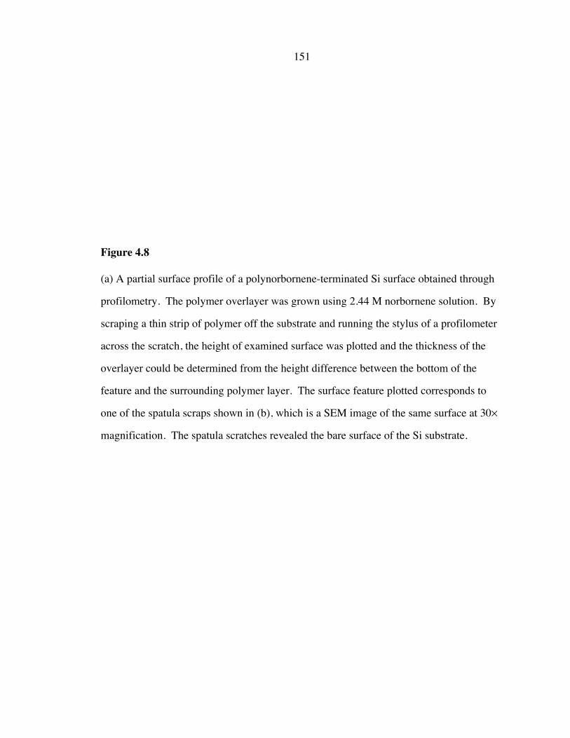
Figure 4.8
(a) A partial surface profile of a polynorbornene-terminated Si surface obtained through
profilometry. The polymer overlayer was grown using 2.44 M norbornene solution. By
scraping a thin strip of polymer off the substrate and running the stylus of a profilometer
across the scratch, the height of examined surface was plotted and the thickness of the
overlayer could be determined from the height difference between the bottom of the
feature and the surrounding polymer layer. The surface feature plotted corresponds to
one of the spatula scraps shown in (b), which is a SEM image of the same surface at 30¥
magnification. The spatula scratches revealed the bare surface of the Si substrate.

152
(a)
-30000
-20000
-10000
0
10000
20000
30000
1000 1200 1400 1600 1800 2000
Hei
ght (
nm)
Distance (µm)
(b)
Stylus Path

153
Figure 4.9
SEM top-view images of two polynorbornene-terminated Si surfaces made from (a) 0.15
M and (b) 2.44 M norbornene/1,2-dichloroethane solutions. The overlayer thicknesses of
two samples were 271 ± 20 Å and 53920 ± 1420 Å, respectively. The samples with
thicker polymer overlayers were found to have larger standard deviations in their
thickness measurements, which can be explained by the SEM image showing a rougher
surface for a thicker overlayer under the same magnification.

154(a)
(b)
50 µm 500¥¥¥¥
50 µm 500¥¥¥¥

155
Figure 4.10
A cross-sectional SEM image of a polynorbornene-covered Si surface at 1500¥
magnification. The polymer film covered the entire Si substrate, and the estimated film
thicknesses at points a, b, and c from the SEM image are 5.0, 5.5, and 5.4 µm,
respectively. These values are in good agreement with the mean polymer thickness of
5.39 ± 0.14 µm that was determined for the same sample using profilometry.
a b c
Si Substrate
PolymerOverlayer
10 µm 1500¥¥¥¥

156
3.3. Photoconductivity Decay Measurements
Time-resolved photoconductivity decay curves of various surfaces are included in
the following sections. Each shown curve is the average of 128 decays, and is fit by a
single exponential to extract the time constant for carrier recombination. The observed
lifetime t can be related to the bulk lifetime tb and the surface recombination velocity S
through this equation:55-57
1 1 2t t= +
b
S
d (4.1)
where d is the sample thickness. The S reported in this chapter were calculated assuming
that the experimentally observed lifetime is dominated by surface recombination with no
contribution from charge-carrier recombination in the bulk (tb = �); therefore, it is
important to note that the reported S values represent the upper limit to the true S values.
3.3.1. C3 Olefin-Terminated and C3 Olefin-Polymer-Terminated Si Surfaces
Figure 4.11 displays the transient photoconductivity decay behaviors of C3 olefin-
terminated, C3 olefin-polynorbornene-terminated, and C3 olefin-polyDCPD-terminated
Si surfaces in an N2(g) ambient. The initial photoconductivity decays of C3-olefin-
modified Si surfaces were relatively slow, with a mean charge-carrier lifetime of 250 ±
60 µs. When a C3 olefin-terminated surface was further modified with either
polynorbornene or polyDCPD, the mean charge-carrier lifetime decreased to 230 ± 90 µs
and 170 ± 10 µs, respectively. The initial S values of these three surfaces were calculated
using Equation 4.1. Assuming an infinite bulk lifetime and d = 294 µm, the upper bound
S values were determined to be 59 ± 10 cm s-1, 64 ± 20 cm s-1, and 88 ± 3 cm s-1,
respectively.

157
Figure 4.12 shows the time-dependent mean carrier lifetimes of all three surfaces
in air (21 ∞C and 7% R.H.). The Si surfaces modified with C3 olefin were not able to
preserve the initial surface quality and the lifetime value dropped very quickly following
the air exposure. Furthermore, the polymer overlayers were found to be ineffective in
protecting the Si surfaces after the C3 olefin layers had failed, and the mean lifetimes of
both polynorbornene- and polyDCPD-modified surfaces also decreased, though not as
quickly as the C3 olefin-terminated Si. Within 5 hours after the C3 olefin-terminated
samples were exposed to the air, the mean lifetime had already exhibited a fivefold
decrease to <50 µs. Within 30 hours of the air exposure, the mean carrier lifetimes of
polymer-terminated surfaces had also dropped to about 50 µs. After being exposed to the
air for 120 hours, C3 olefin- and C3 olefin-polyDCPD-terminated surfaces were found to
have S values of 1600 ± 500 cm s-1 and 610 ± 40 cm s-1. The degradation of the lifetime
for a C3 olefin-terminated surface was very similar to that of an unmodified Si�H surface
in air. Although the polymer overlayers added some protection to the C3 olefin-modified
surfaces, a more effective olefin linker could improve the charge-carrier lifetime at the
modified Si/air interface.
The mean carrier lifetimes of three different C3 olefin-polynorbornene overlayer
thicknesses were also investigated to determine the optimal polymer thickness that
worked the best to preserve the modified surfaces after exposure to the air. Although the
thicker polymer layer was expected to be a better barrier against oxidation of the Si
surface which leads to an increased surface defects, no such trend was observed when the
time-dependent S of samples made using 0.09 M, 0.18 M, and 0.27 M norbornene
solutions were plotted. For following experiments, polynorbornene overlayers made
from a 0.27 M solution were used unless otherwise stated.

158
3.3.2. Effects of Olefin Linker Chain Length
Several terminal olefin linkers were investigated for the purpose of finding the
one that is capable of generating well-preserved surfaces for further modification steps.
Figure 4.13 displays the time dependence of the mean carrier lifetimes of Si surfaces
modified with mixed methyl/allyl (50%:50%, C1/C3 olefin), C3 olefin, C5 olefin, and C6
olefin linkers. With a suspicion that C3 olefin did not provide enough surface coverage
to prevent the oxidation of Si substrate, an olefin layer of better surface coverage was
desired for improving the charge-carrier lifetime of modified Si. Since methyl groups are
small enough to bind to neighboring Si atoms on the surface,58 and may be able to fill in
the pinholes created by C3 olefin modification, methyl Grignard was mixed in with allyl
Grignard to generate mixed C1/C3 olefin-terminated surfaces. However, this mixed
linker was not able to preserve the carrier lifetime, and the S value of this surface
following 90 hour of air exposure was almost as high as that of an unmodified Si�H and a
C3 olefin-terminated surfaces in air, though the rate of the lifetime degradation was
slower for this type of surfaces.
Longer terminal olefin linkers are more flexible and the tilted chains might be
able to cover the surface better. When C6 olefin-terminated Si was found to have a stable
carrier lifetime after 120 hours of air exposure, C5 olefin-terminated surfaces were also
tested. Interestingly, the C5 olefin termination not only had a stable lifetime, but it also
exhibited a longer carrier lifetime. The C5 olefin was therefore used as a linker for all
further surface modifications.
3.3.3. C5 Olefin-Terminated and C5 Olefin-Polymer-Terminated Si Surfaces
Figure 4.14 displays the transient photoconductivity decay behaviors of C5
olefin-terminated, C5 olefin-polynorbornene-terminated, and C5 olefin-polyDCPD-
terminated Si surfaces in an N2(g) ambient. The initial photoconductivity decays of C5-

159
olefin- modified Si surfaces yielded a mean charge-carrier lifetime of 360 ± 10 µs.
Further modification with either polynorbornene or polyDCPD produced surfaces with
mean carrier lifetimes of 200 ± 30 µs and 190 ± 110 µs, which are comparable with the
C5 olefin-polymer modified surfaces. The initial S values of these three surfaces were
calculated using Equation 4.1. Assuming an infinite bulk lifetime and d = 294 µm, the
upper bound S values were determined to be 41 ± 1 cm s-1, 75 ± 10 cm s-1, and 76 ± 50 cm
s-1, respectively.
Figure 4.15 plots the time dependence of the carrier lifetime of each surface in air
under different temperature/humidity conditions. Although the carrier lifetime of C5
olefin-terminated Si was very high initially, it was decreasing very slowly over the course
of 700 hours, and the lifetime drop was slightly more pronounced for samples stored
under the 40 ∞C/80�90% R.H. condition (Figure 4.15a). On the other hand, the carrier
lifetimes of both C5 olefin-polynorbornene- and C5 olefin-polyDCPD- terminated
surfaces were not affected by the storage condition, and the surfaces recombination
velocities remained low after almost one month of air exposure.
Figure 4.16 shows the time-dependent mean carrier lifetimes of all three surfaces
in air (21 ∞C and 7% R.H.); after prolong exposure of these surfaces in air, all still
exhibited low surface recombination velocities. Following 650 hours of air exposure, the
S values were found to be 49 ± 7 cm s-1, 61 ± 10 cm s-1, and 66 ± 10 cm s-1 for C5 olefin-
terminated, C5 olefin-polynorbornene-terminated, and C5 olefin-polyDCPD-terminated
Si surfaces, respectively. The capability for C5 olefin-polymer-terminated surfaces to
reserve the initial low surface-defect-density of the modified Si surfaces in N2(g) was
confirmed.
Figure 4.17 displays the time-dependent mean carrier lifetimes of all three
surfaces in air under an elevated temperature and humidity environment (40 ∞C and
80�90% R.H.). Again, after prolonged exposure of these surfaces in air, all still exhibited
low surface recombination velocities. Following 600 hours of air exposure, the S values
160
were found to be 70 ± 30 cm s-1, 51 ± 8 cm s-1, and 59 ± 10 cm s-1 for C5 olefin-
terminated, C5 olefin-polynorbornene-terminated, and C5 olefin-polyDCPD-terminated
Si surfaces, respectively. Although the mean carrier lifetime of the C5 olefin surfaces has
decreased slightly after 600 hours of air exposure, it was still comparable with the
lifetimes of both polymer-terminated Si. The time-dependent carrier lifetime and surface
recombination velocity data are summarized in Table 4.3.

161
0
0.2
0.4
0.6
0.8
1
1.2
-1.0 -0.5 0.0 0.5 1.0 1.5 2.0 2.5
Si-C3OLSi-C3-PNBSi-C3-DCPD
RF
Pha
se S
hift
(a.
u.)
Time (ms)
Figure 4.11
Time-resolved photoconductivity decay curves of C3 olefin-terminated (squares), C3
olefin-polynorbornene-terminated (circles), and C3 olefin-polyDCPD-terminated
(diamonds) Si surfaces in an N2(g) ambient. The decays were obtained under high-level
injection conditions. Single exponential fits to these decay curves (not shown) yielded a
time constant of 280 µs, 220 µs, and 168 µs, respectively.

162
0
50
100
150
200
250
300
350
0 50 100 150 200
Si-C3OLSi-C3-PNBSi-C3-DCPD
Car
rier
Lif
etim
e (µ
s)
Time Exposed to Air (hr)
Figure 4.12
Time dependence of the mean carrier lifetimes for C3 olefin-terminated (filled
diamonds), C3 olefin-polynorbornene-terminated (open circles), and C3 olefin-
polyDCPD-terminated (open squares) Si in air. The samples were stored in a dark
controlled environmental chamber with an air temperature of 21 ∞C and a relative
humidity of 7% in between measurements. All data were acquired under high-level
injection conditions. The error bars represent the standard deviations for measurements
obtained from at least three samples.

163
0
100
200
300
400
500
0 40 80 120 160 200 240 280
Si-C1C3OLSi-C3OLSi-C5OLSi-C6OL
Car
rier
Lif
etim
e (µ
s)
Time Exposed to Air (hr)
Figure 4.13
Time dependence of the mean carrier lifetimes for mixed methyl/C3 olefin-terminated
(open diamonds), C3 olefin-terminated (filled diamonds), C5 olefin-terminated (open
circles), and C6 olefin-terminated (open squares) Si surfaces in air. The samples were
stored in a dark controlled environmental chamber with an air temperature of 21 ∞C and a
relative humidity of 7% in between measurements. All data were acquired under high-
level injection conditions. The error bars represent the standard deviations for
measurements obtained from at least two samples.

164
0
0.2
0.4
0.6
0.8
1
1.2
-1.0 -0.5 0.0 0.5 1.0 1.5 2.0 2.5
Si-C5OLSi-C5-PNBSi-C5-DCPD
RF
Pha
se S
hift
(a.
u.)
Time (ms)
Figure 4.14
Time-resolved photoconductivity decay curves of C5 olefin-terminated (squares), C5
olefin-polynorbornene-terminated (circles), and C5 olefin-polyDCPD-terminated
(diamonds) Si surfaces in an N2(g) ambient. The decays were obtained under high-level
injection conditions. Single exponential fits to these decay curves (not shown) yielded a
time constant of 366 µs, 273 µs, and 219 µs, respectively.

165
Figure 4.15
Time dependence of the mean carrier lifetimes for (a) C5 olefin-terminated, (b) C5
olefin-polynorbornene-terminated, and (c) C5 olefin-polyDCPD-terminated Si surfaces
exposed to elevated temperature/humidity (open circles) and low temperature/humidity
(filled circles) conditions. The samples exposed to the elevated temperature/humidity
condition were stored in a dark controlled environmental chamber with an air temperature
of 40 ∞C and a relative humidity of 80�90% in between measurements. The samples
exposed to the low temperature/humidity condition were stored in a dark controlled
environmental chamber with an air temperature of 21 ∞C and a relative humidity of 7% in
between measurements. All data were acquired under high-level injection conditions.
The error bars represent the standard deviations for measurements obtained from at least
two samples.

166
0
100
200
300
400
500
0 100 200 300 400 500 600 700
Car
rier
Lif
etim
e (µ
s)
Time Exposed to Air (hr)
Figure 4.15a

167
0
100
200
300
400
500
0 100 200 300 400 500 600 700 800
Car
rier
Lif
etim
e (µ
s)
Time Exposed to Air (hr)
Figure 4.15b

168
0
100
200
300
400
500
0 200 400 600 800
Car
rier
Lif
etim
e (µ
s)
Time Exposed to Air (hr)
Figure 4.15c

169
0
100
200
300
400
500
0 100 200 300 400 500 600 700 800
Si-C5OLSi-C5-PNBSi-C5-DCPD
Car
rier
Lif
etim
e (µ
s)
Time Exposed to Air (hr)
Figure 4.16
Time dependence of the mean carrier lifetimes for C5 olefin-terminated (filled
diamonds), C5 olefin-polynorbornene-terminated (open circles), and C5 olefin-
polyDCPD-terminated (open squares) Si surfaces exposed to a low temperature/humidity
condition. The samples were stored in a dark controlled environmental chamber with an
air temperature of 21 ∞C and a relative humidity of 7% in between measurements. All
data were acquired under high-level injection conditions. The error bars represent the
standard deviations for measurements obtained from at least two samples.

170
0
100
200
300
400
500
0 100 200 300 400 500 600 700 800
Si-C5OLSi-C5-PNBSi-C5-DCPD
Car
rier
Lif
etim
e (µ
s)
Time Exposed to Air (hr)
Figure 4.17
Time dependence of the mean carrier lifetimes for C5 olefin-terminated (filled
diamonds), C5 olefin-polynorbornene-terminated (open circles), and C5 olefin-
polyDCPD-terminated (open squares) Si surfaces exposed to an elevated
temperature/humidity condition. The samples were stored in a dark controlled
environmental chamber with an air temperature of 40 ∞C and a relative humidity of
80�90% in between measurements. All data were acquired under high-level injection
conditions. The error bars represent the standard deviations for measurements obtained
from at least two samples.

171
Table 4.3
Time-dependent measured carrier recombination lifetimes and surface recombination
velocities for various modified Si surfaces. Values of S were calculated assuming an
infinite bulk lifetime.
Overlayer t (µs) S (cm s-1) t (µs) S (cm s-1) t (µs) S (cm s-1)
21 °C/7% R.H.
C3 olefin 250 ± 60 59 ± 10 26 ± 10 570 ± 270 9 ± 3 1600 ± 500
C3 olefin-polynorbornene
230 ± 90 64 ± 20 55 ± 30 270 ± 170 --a --a
C3 olefin-polyDCPD
170 ± 10 88 ± 3 57 ± 5 260 ± 20 24 ± 2 610 ± 40
21 °C/7% R.H.
C5 olefin 360 ± 10 41 ± 1 360 ± 10 41 ± 1 300 ± 40 49 ± 7
C5 olefin-polynorbornene
200 ± 30 75 ± 10 230 ± 40 65 ± 10 240 ± 60 61 ± 10
C5 olefin-polyDCPD
190 ± 110 76 ± 50 220 ± 100 67 ± 30 220 ± 40 66 ± 10
40 °C/80–90% R.H.
C5 olefin 360 ± 30 41 ± 4 370 ± 30 40 ± 4 210 ± 90 70 ± 30
C5 olefin-polynorbornene
230 ± 60 63 ± 20 230 ± 50 63 ± 10 290 ± 50 51 ± 8
C5 olefin-polyDCPD
240 ± 60 61 ± 10 220 ± 70 66 ± 20 250 ± 50 59 ± 10
a Charge-carrier lifetimes were not measured.
In N2( g ) After ~120 hr in AirAfter ~30 hr in Air
After ~150 hr in AirIn N2( g ) After ~600 hr in Air
In N2( g ) After ~150 hr in Air After ~600 hr in Air

172
3.4. Time-Dependent XPS Studies: Oxidation of Modified Si surfaces in Air
While C5 olefin- and C5 olefin-polymer-terminated surfaces exhibited stable
carrier lifetimes when exposed to air under both low temperature/humidity and elevated
temperature/humidity conditions, the effectiveness of the overlayers in preventing the
oxidation of Si substrates was investigated by monitoring the change in the Si 2p region
of XP high-resolution spectra. The thickness of the SiO2 layer was calculated from the
relative areas of the bulk Si 2p and oxidized Si 2p peaks in the high-resolution XP
spectrum. A simple substrate�overlayer model was adapted for this calculation.59,60
dI
I
I
I= +
Ê
ËÁ
�
¯�Ê
ËÁ
�
¯�
È
ÎÍ
ù
ûú
ÏÌÔ
ÓÔ
¸ýÔ
þÔl qov
Si0
ov
ov
Si
sin ln 1 0 (4.2)
where d is the oxide overlayer thickness, lov is the attenuation factor through the oxide
overlayer, q is the angle of the incident x-ray beam from the sample surface, I0Si/I
0ov is an
instrumental normalization factor related to the ratio of the signals expected for pure Si vs
pure SiO2 and Iov/ISi is the ratio of oxidized Si 2p to bulk Si 2p peak areas. Using 2.6 nm
for the value of lov,61 35∞ for q, and 1.3 for I0
Si/I0
ov,60 the thickness of the oxide layer was
determined. The oxide coverage was then estimated using the SiO2 monolayer thickness
of 0.35 nm.62
The time-dependent XP high-resolution spectra of C5 olefin- and C5 olefin-
polyDCPD-terminated Si, oxidized under the two conditions described above, are
displayed in Figure 4.18, Figure 4.19, Figure 4.20, and Figure 4.21. Oxidation of the Si
substrates was observed for both types of surfaces. For C5 olefin modified surfaces, the
amount of SiO2 growth was determined to be 1.00 monolayer after 930 hours of oxidation
in a 21 ∞C/7% R.H. condition and 0.21 monolayers in a 40 ∞C/80�90% R.H. condition for
860 hours. For C5 olefin-polyDCPD modified surfaces, the SiO2 growth was 3.04

173
monolayers and 1.75 monolayers, respectively. In the case of oxidation under the
21 ∞C/7% R.H. condition, the amount of SiO2 growth increased with the length of
oxidation time. When samples were exposed to the elevated temperature/humidity
condition, the oxide growth rate was faster but less overall oxide growth was observed
for equivalent oxidation time lengths. For example, in an elevated temperature/humidity
condition, the amount of oxide growth on a Si-C5 olefin-polyDCPD during the first 97
hours of oxidation was about the same as for the same type of surface to be oxidized in
the low temperature/humidity condition for 384 hours. The oxide growth at an elevated
temperature/humidity condition had also reached its maximum when the spectrum was
collected after 97 hours of exposure time, while the oxide growth continued for samples
stored under the low temperature/humidity condition. For comparison, the XP high-
resolution spectra of the Si 2p region showing the time-dependent air oxidation of a
hydrogen-terminated Si are displayed in Figure 4.22. The amount of oxide on the Si
surface was determined to be 1.10 monolayers after 946 hours of air exposure at
21 ûC/7% R.H. A summary of the oxide growth monitored by XPS is displayed in
Table 4.4.

174
9899100101102103104
(a) 0 hr(b) 72 hr(c) 176 hr(d) 387 hr(e) 933 hr
Inte
nsit
y (a
.u.)
Binding Energy (eV)
Figure 4.18
High-resolution XP spectra of C5 olefin-terminated Si focusing on the Si 2p region
collected (a) before exposing the surface to the air, (b) after 72 hours, (c) after 176 hours,
(d) after 387 hours, and (e) after 933 hours of air exposure, under low
temperature/humidity condition. The samples were stored in a dark controlled
environmental chamber with an air temperature of 21 ∞C and a relative humidity of 7% in
between measurements. These spectra were normalized relative to the intensity of bulk
Si 2p peak (98.5�100.4 eV binding energies).

175
9899100101102103104
(a) 0 hr(b) 100 hr(c) 303 hr(d) 857 hr
Inte
nsit
y (a
.u.)
Binding Energy (eV)
Figure 4.19
High-resolution XP spectra of C5 olefin-terminated Si focusing on the Si 2p region
collected (a) before exposing the surface to the air, (b) after 100 hours, (c) after 303
hours, and (d) after 857 hours of air exposure, under elevated temperature/humidity
condition. The samples were stored in a dark controlled environmental chamber with an
air temperature of 40 ∞C and a relative humidity of 80�90% in between measurements.
These spectra were normalized relative to the intensity of bulk Si 2p peak (98.5�100.4 eV
binding energies).

176
9899100101102103104
(a) 0 hr(b) 70 hr(c) 174 hr(d) 384 hr(e) 931 hr
Inte
nsit
y (a
.u.)
Binding Energy (eV)
Figure 4.20
High-resolution XP spectra of C5 olefin-polyDCPD-terminated Si focusing on the Si 2p
region collected (a) before exposing the surface to the air, (b) after 70 hours, (c) after 174
hours, (d) after 384 hours, and (e) after 931 hours of air exposure, under low
temperature/humidity condition. The samples were stored in a dark controlled
environmental chamber with an air temperature of 21 ∞C and a relative humidity of 7% in
between measurements. These spectra were normalized relative to the intensity of bulk
Si 2p peak (98.5�100 eV binding energies).

177
9899100101102103104
(a) 0 hr(b) 97 hr(c) 309 hr(d) 854 hr
Inte
nsit
y (a
.u.)
Binding Energy (eV)
Figure 4.21
High-resolution XP spectra of C5 olefin-polyDCPD-terminated Si focusing on the Si 2p
region collected (a) before exposing the surface to the air, (b) after 97 hours, (c) after 309
hours, and (d) after 854 hours of air exposure, under elevated temperature/humidity
condition. The samples were stored in a dark controlled environmental chamber with an
air temperature of 40 ∞C and a relative humidity of 80�90% in between measurements.
These spectra were normalized relative to the intensity of bulk Si 2p peak (98.5�100.4 eV
binding energies).

178
9899100101102103104
(a) 0 hr(b) 88 hr(c) 192 hr(d) 405 hr(e) 946 hr
Inte
nsit
y (a
.u.)
Binding Energy (eV)
Figure 4.22
High-resolution XP spectra of H-terminated Si focusing on the Si 2p region collected (a)
before exposing the surface to the air, (b) after 88 hours, (c) after 192 hours, (d) after 405
hours, and (d) after 946 hours of air exposure, under low temperature/humidity condition.
The samples were stored in a dark controlled environmental chamber with an air
temperature of 21 ∞C and a relative humidity of 7% in between measurements. These
spectra were normalized relative to the intensity of bulk Si 2p peak (99.2�101 eV binding
energies).

179
Table 4.4
Time dependence of the silicon oxide growth for C5 olefin-terminated and C5 olefin-
polyDCPD-terminated Si under both low and elevated temperature/humidity conditions,
and for the H-terminate Si under low temperature/humidity condition.
Time Exposed to Air (hr)
Oxidized Si 2p /Bulk Si 2p
Calculated Oxide Layer Thicknessa
(nm)
Equivalent Monolayers SiOx
b
72 0.004 0.008 0.02176 0.108 0.195 0.56487 0.116 0.209 0.60933 0.203 0.349 1.00
303 0.057 0.106 0.30857 0.039 0.074 0.21
70 0.064 0.120 0.34174 0.386 0.607 1.73384 0.471 0.713 2.04931 0.799 1.063 3.04
97 0.503 0.751 2.15309 0.406 0.633 1.81854 0.389 0.611 1.75
88 0.037 0.070 0.20192 0.072 0.134 0.38405 0.121 0.219 0.62946 0.226 0.383 1.10
Si-H in 21 °C/7% R.H.
a Calculated using Equation 4.2, where the escape depth of the Si 2p electron through an oxide overlayer was taken to be 2.6 nm, q = 35û, and the I 0
Si/I 0ov in the
Si 2p region was determined to be 1.3.b The thickness of a monolayer of SiO2 was estimated to be 0.35 nm.
Si-C5 olefin in 21 °C/7% R.H.
Si-C5 olefin in 40 °C/80–90% R.H.
Si-C5 olefin-polyDCPD in 21 °C/7% R.H.
Si-C5 olefin-polyDCPD in 40 °C/80–90% R.H.

180
4. Discussions
4.1. Surface Modifications and Characterizations
Extended from the two-step chlorination/alkylation reaction developed previously
in our laboratory, a reaction sequence was advanced for the modification of Si(111)
surfaces with polymers. This method would appear to be general in that a wide range of
monomers can be polymerized with 121,44,54,63 and could be used to form overlayers of
controlled thicknesses on Si surfaces. When the first polymer layer is electrically
insulating (as in the present case), this method should allow formation of metal-insulator-
semiconductor structures or of capacitors of controlled thickness, whereas when the first
polymer is metallic or semiconducting in nature (e.g., when cyclooctatetraenes,
phenylenevinylenes, etc,. are used as feedstocks64), the process should provide a route to
formation of semiconductor/metal or semiconductor heterojunction structures. Because
the polymer was attached to the substrate through a covalent linkage, the polymer
overlayer was robust and a relatively uniform growth was afforded as seen in SEM
images.
Although XPS data were useful in providing evidences for each step of the
surface modification process, there was a limitation that prevented us from obtaining a
direct XPS confirmation for the binding of Ru catalysts to the olefin-terminated Si
surfaces. The intensity of the Ru signal is expected to be very low when a relatively large
amount of C can be detected on the surface. Assuming that reagent 1 has bound onto
50% of the total available groups in a monolayer of olefin on the Si surface implies a
1:41 Ru/C ratio for the atoms in the overlayer. With the atomic sensitivity factors of Ru
3d5/2 and C 1s being 1.55 and 0.205, respectively,65 the area of the expected Ru 3d5/2 peak
is calculated to be 18% of the C 1s signal. Because both the Ru 3d5/2 and Ru 3d3/2 peak

181
positions are within 5 eV of the C 1s peak, observation of such small Ru peaks in the
presence of a large C 1s signal is not readily possible with our XPS instrument (VG
Instruments M-probe Spectrometer, with a full width at half maximum of 1.50 ± 0.01 eV
for the Au 4f7/2 peak in survey scan mode). Although the Ru 3p3/2 peak does not overlap
with C 1peak, the Ru 3p3/2 peak is about 1/3 as intense as the Ru 3d5/2 peak. Since the
estimated relative peak area of the Ru 3p3/2 is only 6% of the C 1s peak area, it can not be
resolved in the XP spectra of our polymer-terminated samples. Alternatively, the control
experiments were used to establish the necessity of the presence of surface-bound Ru
complexes for the formation of robust polymer overlayers. The presence of a polymer
overlayer with a good coverage was also confirmed by the SEM results.
Both norbornene and DCPD were readily polymerized on Si surfaces using
catalyst 1 as an initiator. Although bulk metathesis polymerization of COD using
catalysts 1 and 2 and COT using catalyst 2 has been reported previously,64,66 surface-
initiated ROMP of either COD or COT on Si(111) was not successful. When a Si surface
was first coated with catalyst 1 by adding a few drops of 25 mM catalyst solution and the
solvent was allowed to evaporate, a polymer film was observed following addition of
COD to the catalyst-coated Si. The result suggested that while the surface-bound Ru
catalyst was able to ROMP the highly strained norbornene; the concentration of surface-
bound catalyst may not be high enough to permit detectable surface-initiated ROMP of
less-strained COD and COT. The binding of a Ru complex to an olefin linker requires
the complex to line up with the double bond of the linker in a certain way, and this can be
quite difficult when the linker is fixed on the Si surface. The large dimensions of Ru
molecules also post a geometric limitation (see Figure 4.23) which does not allow all
olefin linkers on the substrate to bind with Ru; therefore, the low concentration of the
surface-bound catalyst is suspected to impede the successful ROMP of less-strained ring
monomers.

182
Another problem encountered during the Si surface modification process was the
possible introduction of silicon oxide. The surface modification process involved was
very sensitive to any oxygen source including methanol vapor that might be present in the
N2(g)-purged glove box. When the surface modification took place without first
eliminating as much methanol vapor as possible, and when septa-capped test tubes were
used instead of screw-capped, the success rate for producing oxide-free modified surfaces
was very low. During the overnight heated Grignard reaction, the methanol vapor can be
drawn into the reaction vessels and can provide the Si with oxygen needed for oxidation.
By placing a wide-mouth bottle containing fresh P2O5 powders in the glove box before
and during the reaction, the P2O5 could absorb methanol vapor and reduced the amount of
volatile oxygen source. The reaction tubes were also capped tightly to ensure minimal
exposure of the reaction contents to the glove box atmosphere.
Other factors that might affect the success rate of surface modification include the
freshness of reagents and the possibility of the contamination of rinsing solvents. While
the monomer solutions can be stored in aluminum foil-wrapped Schlenk tubes inside the
glove box, it is best to use freshly made monomer solutions to assure that the correct
monomer concentration was used. There is always a possibility for monomers to
polymerize in the Schlenk tube if the solution was contaminated by any catalyst
molecule, and this could lead to a lower than expected monomer concentration for
polymerization on the substrate. The Grignard reagents purchased from Aldrich should
only be used within one month after opening the bottle in the glove box. It is also best to
keep the Sure/Seal caps on for all solvents and reagents, and use only syringes to
dispense all liquids.

183
Figure 4.23
A space-filling model showing the relative sizes of the Ru catalyst and the Si surface
atoms. The Si surface is covered with C3 olefin linkers. Since the cross section of a Ru
complex is much larger than that of an olefin linker, the number of surface-bound Ru
molecules is expected to be less than 50% of the number of linkers. The Ru addition
requires a cross metathesis reaction between the Ru=C double bond and the terminal C=C
double bond of the olefin linker.
Ru complex
Si substrate
C3 olefinlinker
P
Cl
Ru
CH
Si

184
4.2. Surface Recombination Velocity and Oxidation
The transient photoconductivity decay behaviors of modified Si surfaces were
studied to further investigate the effects of surface modification on the electrical
properties of Si. The results indicated the lack of silicon oxide formation during the
surface-initiated ROMP of both norbornene and DCPD, and covalently attached polymer
overlayers were grown on the Si surfaces. The initial photoconductivity decay
measurements of C3 olefin-terminated, C3 olefin-polynorbornene-terminated, and C3
olefin-polyDCPD-terminated Si in an N2(g) ambient showed that the surface modification
procedure did not greatly affect the desirable electrical properties of Si, and all three
types of surfaces exhibited low defect density following the reactions. However, the
charge-carrier recombination lifetimes decreased quickly upon exposure to an air
ambient, suggesting that the attached overlayers were ineffective in preventing the
surface degradation of Si in air. When the time dependence of mean carrier lifetimes of
these three surfaces were compared, the rates of decreasing lifetime were slower for both
polymer-terminated surfaces, despite having shorter initial lifetimes than that of olefin-
terminated Si.
When longer terminal olefin linkers, specifically C5 and C6 olefins, were used,
the mean carrier lifetimes did not drop upon air exposure. In fact, C5 olefin-terminated
surface was found to have an initial lifetime >350 µs, and was capable of preserving the
long lifetime for at least 300 hours in air. Presumably the C5 and C6 olefin chains were
more flexible while fixed onto the Si surfaces, the slight tilt of these chains could
possibly cover some potential oxidation sites and decrease the chances of defect
formation. Subsequent growth of polymer overlayers on top of the C5 olefin resulted in
slightly shorter initial lifetimes, but both C5 olefin-polynorbornene- and C5 olefin-
polyDCPD-terminated Si were capable of keeping the mean carrier lifetimes at

185
200�300 µs for about one month. The surface recombination velocity can be related to
the surface defect density using the equation:12,57
2S N= t thu s (3.3)
where Nt is the number of recombination centers per square centimeter, uth is the carrier
thermal velocity (taken to be ª107 cm s-1), and s is the carrier-capture cross section.
Assuming the s is 10-15 cm2, these polymer-terminated Si surfaces would have surface
defect density of (0.98�1.5) ¥ 1010 cm-2. This is equivalent to having a low defect density
of less than one active electrical defect site for every ª 68,000 surface atoms. This
surface modification sequence using C5 olefin as a linker could therefore prove useful in
providing means to functionalize Si without jeopardizing the electrical properties
necessary for device applications.
While further XPS analysis of C5 olefin- and C5 olefin-polyDCPD-terminated
surfaces revealed silicon oxide formation in an air ambient, the persisting slow surface
recombination velocities indicated that the polymer overlayers were still effective in
preventing electrical degradation of Si when oxidized. The oxide layer thickness was
calculated with an assumption that ejected electrons from both bulk Si and Si oxide were
attenuated by the polymer overlayer of a uniform density and thickness. However, if the
oxide only grew from Si atoms that were not modified due to geometric limitation of the
olefin linker, it is possible that the region of polymer overlayer above the oxide was less
dense than the region above a grafting point. In this case, a larger portion of total
electrons ejected from Si oxide would escape through the polymer overlayer and being
collected by the analyzer compared to the number of escaped electrons originated from
the bulk Si. The result would then be translated into a larger oxidized/bulk Si 2p peak
ratio and a thicker calculated oxide film. The unusually large oxidized Si oxide peaks
observed in the XP spectra of the polyDCPD-terminated surface may be the consequence

186
of this density variation, and the reported Si oxide thicknesses for this samples may not
represent the true values.
Figure 4.24 displays the Si 2p high-resolution XP spectra of oxidized H-
terminated, C5 olefin-terminated, and C5 olefin-polyDCPD-terminated Si surfaces after
~930 hours of air exposure under low temperature/humidity condition. A comparison of
the oxidized Si 2p peak positions of these samples was made to elucidate the differences
in surface oxides that gave rise to very different S. When spectra were shifted to line up
bulk Si 2p peaks of these three surfaces, the Si oxide peaks of both C5 olefin-terminated
and polyDCPD-terminated surfaces appeared at a slightly higher binding energy
compared to that of the air-oxidized H-terminated surface. This finding suggests that a
different kind of Si oxide was formed when C5 olefin-terminated and C5 olefin-polymer-
modified Si were exposed to air, and this oxide formation did not create additional
surface defects that could cause the S to rise. The oxide thickness was very similar
between H-terminated and C5 olefin-terminated Si oxidized under the low
temperature/humidity condition, but the carrier lifetime of the H-terminated Si was
substantially shorter, recorded at as low as 6 µs after 900 hours of air exposure. The
ability for C5 olefin-polymer-terminated Si to persist low surface defect density despite
the formation of Si oxide when stored in air under both low and elevated
temperature/humidity conditions proved the excellence and usefulness of this general
surface modification method. This reaction sequence can provide a simple route to grow
robust and uniform overlayers of polymers and block copolymers with different
functionalities on Si surfaces, especially for novel applications in electrical devices
requiring low surface recombination velocity.

187
9899100101102103104
H (946 hr)
C5 olefin (933 hr)
polyDCPD (931 hr)
Inte
nsit
y (a
.u.)
Binding Energy (eV)
Figure 4.24
The Si 2p high-resolution XP spectra of H-terminated ( ), C5 olefin-terminated
( ), and C5 olefin-polyDCPD-terminated ( ) surfaces. The spectra were
normalized relative to the intensity of bulk Si 2p peak. The silicon oxide peak positions
of both polymer-terminated surfaces shifted to slightly lower binding energy, indicating a
different kind of silicon oxide was formed.

188
5. Summary
The growth of robust polymer films that are covalently attached to Si surfaces via
a Si-C linkage was demonstrated. Uniform layers of different polymers were formed
using a general method combining chlorination/Grignard reaction with ring-opening
metathesis polymerization (ROMP). The surfaces of these modified Si were
characterized by XPS, SEM, ellipsometry, and/or profilometry. Varying the
concentration of monomer can control the thickness of the polymer overlayer, so that
polymer thicknesses between 0.9 and 5500 nm can be achieved. The charge-carrier
dynamics at olefin- and polymer-terminated Si/air interfaces was investigated using
transient photoconductivity decay method. The C5 olefin was determined to be the
optimal linker that is capable of preserving the electrical properties of the Si(111) surface
when exposed to air. Time-dependent photoconductivity measurements further
confirmed the ability for both polynorbornene-terminated and polyDCPD-terminated Si
to maintain low surface recombination velocities in air for a period of one month, under
both low and elevated temperature/humidity conditions. Instead of acting as a physical
barrier against oxidation, the polymer overlayer allows the formation of non-deleterious
Si oxide that does not introduce defect site on the surface. This �graft from� method is
proven to be a general and simple way to modify Si surfaces with cyclic and derivatized
cyclic polymers for future electronic device applications.
6. Acknowledgments
I thank Oren A. Scherman for the collaboration and for the synthesis of Grignard
reagents. This work was supported by the National Science Foundation, CHE-9974562
(N.S.L.), and by the Air Force Office of Scientific Research, Grant F49620-96-0035
(R.H.G.).

189
7. References
(1) Bansal, A.; Lewis, N. S. J. Phys. Chem. B 1998, 102, 4058.
(2) Sailor, M. J.; Klavetter, F. L.; Grubbs, R. H.; Lewis, N. S. Nature 1990, 346, 155.
(3) Huck, W. T. S.; Yan, L.; Stroock, A.; Haag, R.; Whitesides, G. M. Langmuir
1999, 15, 6862.
(4) Clark, S. L.; Montague, M.; Hammond, P. T. Supramol. Sci. 1997, 4, 141.
(5) Whidden, T. K.; Ferry, D. K.; Kozicki, M. N.; Kim, E.; Kumar, A.; Wilbur, J.;
Whitesides, G. M. Nanotechnology 1996, 7, 447.
(6) Sailor, M. J.; Ginsburg, E. J.; Gorman, C. B.; Kumar, A.; Grubbs, R. H.; Lewis,
N. S. Science 1990, 249, 1146.
(7) Bansal, A.; Lewis, N. S. J. Phys. Chem. B 1998, 102, 1067.
(8) Royea, W. J.; Juang, A.; Lewis, N. S. Appl. Phys. Lett. 2000, 77, 1988.
(9) Sze, S. M. The Physics of Semiconductor Devices; 2nd ed.; Wiley: New York,
1981.
(10) Royea, W. J.; Michalak, D. J.; Lewis, N. S. Appl. Phys. Lett. 2000, 77, 2566.
(11) Eades, W. D.; Swanson, R. M. J. Appl. Phys. 1985, 58, 4267.
(12) Yablonovitch, E.; Gmitter, T. J. Solid State Elec. 1992, 35, 261.
(13) Aberle, A. G.; Glunz, S.; Warta, W. J. Appl. Phys. 1992, 71, 4422.
(14) Ulman, A. An Introduction to Ultrathin Organic Films; Academic Press: Boston,
1991.
(15) Hadziioannou, G.; Patel, S.; Granick, S.; Tirrell, M. J. Am. Chem. Soc. 1986, 108,
2869.
(16) Belder, G. F.; tenBrinke, G.; Hadziioannou, G. Langmuir 1997, 13, 4102.
(17) Dan, N.; Tirrell, M. Macromolecules 1993, 26, 6467.
(18) Lenk, T. J.; Hallmark, V. M.; Rabolt, J. F.; Haussling, L.; Ringsdorf, H.
Macromolecules 1993, 26, 1230.
(19) Jordan, R.; Graf, K.; Riegler, H.; Unger, K. K. Chem. Commun. 1996, 1025.
(20) Ebata, K.; Furukawa, K.; Matsumoto, N. J. Am. Chem. Soc. 1998, 120, 7367.
(21) Kim, N. Y.; Jeon, N. L.; Choi, I. S.; Takami, S.; Harada, Y.; Finnie, K. R.;
Girolami, G. S.; Nuzzo, R. G.; Whitesides, G. M.; Laibinis, P. E. Macromolecules
2000, 33, 2793.
(22) Jordan, R.; Ulman, A. J. Am. Chem. Soc. 1998, 120, 243.
(23) Jordan, R.; Ulman, A.; Kang, J. F.; Rafailovich, M. H.; Sokolov, J. J. Am. Chem.
Soc. 1999, 121, 1016.
(24) Prucker, O.; Ruhe, J. Macromolecules 1998, 31, 602.

190
(25) Zhao, B.; Brittain, W. J. Macromolecules 2000, 33, 8813.
(26) Ingall, M. D. K.; Joray, S. J.; Duffy, D. J.; Long, D. P.; Bianconi, P. A. J. Am.
Chem. Soc. 2000, 122, 7845.
(27) Husseman, M.; Malmstrom, E. E.; McNamara, M.; Mate, M.; Mecerreyes, D.;
Benoit, D. G.; Hedrick, J. L.; Mansky, P.; Huang, E.; Russell, T. P.; Hawker, C. J.
Macromolecules 1999, 32, 1424.
(28) Boukherroub, R.; Wayner, D. D. M. J. Am. Chem. Soc. 1999, 121, 11513.
(29) Sieval, A. B.; Vleeming, V.; Zuilhof, H.; Sudholter, E. J. R. Langmuir 1999, 15,
8288.
(30) Boukherroub, R.; Morin, S.; Bensebaa, F.; Wayner, D. D. M. Langmuir 1999, 15,
3831.
(31) Sieval, A. B.; Demirel, A. L.; Nissink, J. W. M.; Linford, M. R.; van der Maas, J.
H.; de Jeu, W. H.; Zuilhof, H.; Sudholter, E. J. R. Langmuir 1998, 14, 1759.
(32) Linford, M. R.; Chidsey, C. E. D. J. Am. Chem. Soc. 1993, 115, 12631.
(33) Linford, M. R.; Fenter, P.; Eisenberger, P. M.; Chidsey, C. E. D. J. Am. Chem.
Soc. 1995, 117, 3145.
(34) Zazzera, L. A.; Evans, J. F.; Deruelle, M.; Tirrell, M.; Kessel, C. R.; Mckeown, P.
J. Electrochem. Soc. 1997, 144, 2184.
(35) Feng, W. J.; Miller, B. Langmuir 1999, 15, 3152.
(36) Effenberger, F.; Gotz, G.; Bidlingmaier, B.; Wezstein, M. Angew. Chem.-Int.
Edit. 1998, 37, 2462.
(37) Allongue, P.; de Villeneuve, C. H.; Pinson, J.; Ozanam, F.; Chazalviel, J. N.;
Wallart, X. Electrochim. Acta 1998, 43, 2791.
(38) He, J.; Patitsas, S. N.; Preston, K. F.; Wolkow, R. A.; Wayner, D. D. M. Chem.
Phys. Lett. 1998, 286, 508.
(39) deVilleneuve, C. H.; Pinson, J.; Bernard, M. C.; Allongue, P. J. Phys. Chem. B
1997, 101, 2415.
(40) Wagner, P.; Nock, S.; Spudich, J. A.; Volkmuth, W. D.; Chu, S.; Cicero, R. L.;
Wade, C. P.; Linford, M. R.; Chidsey, C. E. D. J. Struct. Biol. 1997, 119, 189.
(41) Hamers, R. J.; Coulter, S. K.; Ellison, M. D.; Hovis, J. S.; Padowitz, D. F.;
Schwartz, M. P.; Greenlief, C. M.; Russell, J. N. Accounts Chem. Res. 2000, 33,
617.
(42) Schwartz, M. P.; Ellison, M. D.; Coulter, S. K.; Hovis, J. S.; Hamers, R. J. J. Am.
Chem. Soc. 2000, 122, 8529.
(43) Bansal, A.; Li, X.; Lauermann, I.; Lewis, N. S.; Yi, S. I.; Weinberg, W. H. J. Am.
Chem. Soc. 1996, 118, 7225.

191
(44) Weck, M.; Jackiw, J. J.; Rossi, R. R.; Weiss, P. S.; Grubbs, R. H. J. Am. Chem.
Soc. 1999, 121, 4088.
(45) Scholl, M.; Ding, S.; Lee, C. W.; Grubbs, R. H. Org. Lett. 1999, 1, 953.
(46) Higashi, G. S.; Chabal, Y. J.; Trucks, G. W.; Raghavachari, K. Appl. Phys. Lett.
1990, 56, 656.
(47) Hassler, K.; Koll, W. J. Organomet. Chem. 1995, 487, 223.
(48) Wyman, D. P.; Wang, J. Y. C.; Freeman, W. R. J. Org. Chem. 1963, 28, 3173.
(49) Stinespring, C. D.; Wormhoudt, J. C. J. Appl. Phys. 1989, 65, 1733.
(50) Cheng, K. L. Japan. J. Appl. Phys. 1995, 34, 5527.
(51) Tufts, B. J.; Kumar, A.; Bansal, A.; Lewis, N. S. J. Phys. Chem. 1992, 96, 4581.
(52) Mende, G.; Finster, J.; Flamm, D.; Schulze, D. Surf. Sci. 1983, 128, 169.
(53) Schwab, P.; Grubbs, R. H.; Ziller, J. W. J. Am. Chem. Soc. 1996, 118, 100.
(54) Amir-Ebrahimi, V.; Corry, D. A.; Hamilton, J. G.; Thompson, J. M.; Rooney, J. J.
Macromolecules 2000, 33, 717.
(55) Kunst, M.; Sanders, A. Semicond. Sci. Techno. 1992, 7, 51.
(56) Yablonovitch, E.; Swanson, R. M.; Eades, W. E.; Weinberger, B. R. Appl. Phys.
Lett. 1986, 48, 245.
(57) Yablonovitch, E.; Allara, D. L.; Chang, C. C.; Gmitter, T.; Bright, T. B. Phys.
Rev. Lett. 1986, 57, 249.
(58) Bansal, A.; Li, X.; Yi, S. I.; Weinberg, W. H.; Lewis, N. S. J. Phys. Chem. B
2001, 105, 10266.
(59) Briggs, D.; Seah, M. P. Practical Surface Analysis: Auger and X-Ray
Photoelectron Spectroscopy; 2nd ed.; Wiley: New York, 1990; Vol. 1.
(60) Pomykal, K. E.; Fajardo, A. M.; Lewis, N. S. J. Phys. Chem. 1995, 99, 8302.
(61) Hochella, M. F., Jr.; Carim, A. H. Surf. Sci. 1988, 197, L260.
(62) Haber, J. A.; Lewis, N. S. J. Phys. Chem. B 2002, 106, 3639.
(63) Maughon, B. R.; Morita, T.; Bielawski, C. W.; Grubbs, R. H. Macromolecules
2000, 33, 1929.
(64) Scherman, O. A.; Grubbs, R. H. Synth. Metals 2001, 124, 431.
(65) Wagner, C. D.; Riggs, W. M.; Davis, L. E.; Moulder, J. F. Handbook of X-Ray
Photoelectron Spectroscopy; Perkin-Elmer Corporation: Eden Prairie, MN, 1979.
(66) Bielawski, C. W.; Scherman, O. A.; Grubbs, R. H. Polymer 2001, 42, 4939.