chapter 3 fabrication and characterization of n-si(111...
TRANSCRIPT

74
Chapter 3
Fabrication and Characterization of n-Si(111)
Based Metal-Insulator-Semiconductor Diodes

75
1. Introduction
Our knowledge of metal-semiconductor diodes goes back more than a century ago
when Braun,1 in 1874, discovered the rectifying nature of metallic contacts on
semiconductors such as copper, iron, and lead sulfide crystals.2 It was not until 1931,
when Schottky3 proposed the existence of some sort of potential barrier at the metal-
semiconductor contact, that the scientists began to understand the rectifying nature of this
junction. In 1938, Schottky4 and Mott5 pointed out, independently, that the potential
barrier formation was the result of a difference between the work functions of the metal
and semiconductor, and the metal-semiconductor barrier height (fb) could be calculated
according to this equation:
f j cb m s= -( ) / q (3.1)
where jm is the metal work function and cs is the electron affinity of the semiconductor.
This behavior has come to be known as the �Schottky limit.�
Practical metal-semiconductor contacts do not always appear to obey the Schottky
limit. Linear dependence of the barrier height on metal work function is predominantly
observed in ionic semiconductors only. In the case of covalent semiconductors, some
have barrier heights that are only weakly dependent on jm, and some exhibit almost no
relationship between fb and jm.6 Bardeen7 was the first to point out the importance of
localized surface states, which exist in many covalent semiconductors, in determining the
barrier height. These surface states arise from the dangling bonds at the semiconductor
surface where no neighboring atoms are available for making covalent bond on the
vacuum side, and their energies are usually continuously distributed across the bandgap.
When brought into contact with a metal, equilibration between Fermi levels of these two
phases occurs first by exchanging charges between the metal and the surface states,
76
which then reduces or eliminates the effect on the semiconductor depletion region.2 As a
result the barrier height is primarily determined by the surface states and is largely
independent of the metal in contact. A system that obeys this �Bardeen limit� is
described as �Fermi-level pinned.�
Heine8 argued that when a metal is deposited on a semiconductor surface, it is
possible for the wave function of electrons in the metal with energies corresponding to
the forbidden gap in the semiconductor to extend into the semiconductor and thereby
induce states within the bandgap. These metal induced gap states (MIGS) replace the
intrinsic electron states that may be present on the semiconductor surface, and can affect
the true barrier height measurements.
In some cases, when a metal is deposited on a semiconductor surface, an
interfacial reaction between the metal and the semiconductor occurs to form deleterious
silicide. This interfacial reaction causes the interface to move into the semiconductor
bulk, and as a result the barrier height is independent of the surface properties and the
metal work function.9-11,12 ,13 It was found that the barrier heights of this type of MS
contacts are linearly dependent on the heat of formation of the silicide.14 In these cases
the properties of the silicides controls barrier formation, which prevents the true barrier
height of the MS contacts to be determined.
A thin-film insulator, namely thermally grown oxide, has been used to make
metal-insulator-semiconductor (MIS) contacts since the mid-60�s. A native thin oxide
layer on the semiconductor surface is thin enough that a significant number of electrons
can tunnel through it, and it also satisfies the dangling bonds and thus reduces the
intrinsic surface state density. However, thermally grown oxides on silicon typically
contain fixed positive charges, which increase the barrier height of p-type Si junctions,
but have an opposite effect on n-type Si junctions.15 Some metals can also penetrate
through a thin layer of oxide, and react with the semiconductor to form silicide.
Although it�s now possible to control oxide layer thicknesses on the order of angstroms,

77
oxide layers tend to grow thicker over time and consequently lower the current that was
allowed to tunnel through.
An alkyl monolayer can serve as a useful alternative to the oxide layer in MIS
devices, because its thickness is easily controlled down at an atomic level. Since such
layers can be covalently attached to the Si surface, they also satisfy the dangling bonds
and reduce the density of surface states. Since the interactions between the independent
alkyl chains and the Si atoms are covalent, they can align themselves in registry with the
Si atoms better than the lattice-constrained oxygen atoms in SiO2. Many alkyl groups
have been covalently attached to Si(111) surfaces via a two-step chlorination/alkylation
procedure.16-18 This modification technique could be utilized to develop a MIS system
enabling barrier height measurements of intimate metal-semiconductor contacts not
currently possible. For an improved MIS system with an alkyl insulating layer, the
observed fb value should be closer to the Schottky limit. Another advantage of using an
alkyl insulator is that the thickness is easily controlled by using different chain lengths,
and thus reproducible thicknesses can be achieved for systematic investigation of its
effects on the junction electrical properties. Barrier height measurements and J–E
characterization of the MIS with different insulator thickness could identify an optimal
alkyl chain that can effectively inhibit silicide formation while introducing the minimal
series resistance.
Introduction of a thin insulating layer between a metal and a semiconductor could
affect the J�E characteristics of an MS contact in many ways. An insulating layer could
reduce the number of majority carriers crossing the interface from the semiconductor into
the metal, decrease the reverse saturation current density (J0) , and therefore increase the
open-circuit voltage (Voc). It could also act as a chemical barrier and prevent unfavorable
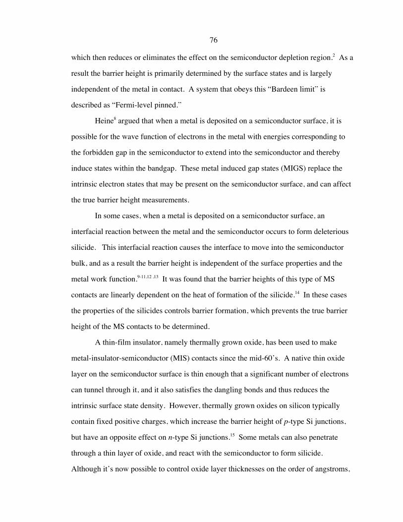
interfacial reactions between the metal and the semiconductor. As depicted in Figure 3.1,
voltage drop typically occurs at a MIS interface due to the resistance of the insulator.
However, when the insulating layer is very thin (i.e., < 20 Å), the potential drop across it

78
should be negligibly small compared to that in the semiconductor depletion region,2 and
electrons should be able to tunnel through this layer relatively easily. Straight alkyl
chains tend to line up on a surface and form an organized overlayer, which will also
encourage electron tunneling. In this case, the barrier height and the contact potential
difference should be unaffected by the presence of the thin interfacial layer, and the true
MS barrier height can be extracted for silicide-forming metal/Si interfaces.
79
jm
cs
EF
Ecb
Evb
qfbqVbi
Evacuum
MetalSemiconductor
EF,mW
Insulating Layer
Ene
rgy
(eV
)
(+)
(�)
Figure 3.1
A band bending diagram of a metal-insulator-semiconductor (MIS) junction. The barrier
height (fb) of this junction is less than the difference between the metal work function
(jm) and the electron affinity of the semiconductor (cs), and it is caused by a voltage drop
across the insulating layer. If the insulating layer is thin enough, the voltage drop can
become negligible, and can mimic the electrical properties of the equivalent
metal/semiconductor junction.

80
2. Experimental
2.1. Solvents and Reagents
All solvents used for surface modification, including anhydrous methanol,
anhydrous chlorobenzene, anhydrous acetonitrile, and anhydrous tetrahydrofuran (THF)
were obtained from Aldrich and were used as received. These solvents were packaged
under N2(g) in Sure/Seal bottles and were stored over activated 3 Å molecular sieves (EM
Science) in a N2(g)-purged glove box. Solvents used for wafer degreasing, acetone,
dichloromethane, methanol, and 1,1,1-trichloroethane, were either reagent grade (GR) or
Omnisolve grade obtained from EM Science and used as received. The 30% H2O2 was
purchased from EM Science, and the H2SO4(aq) was obtained from J. T. Baker.
Hydrofluoric acid buffered with ammonium fluoride (NH4F/HF, buffered HF) and 40%
ammonium fluoride (NH4F) solutions were purchased from Transene Co. The 18 MW◊cm
resistivity H2O was collected from a Barnstead E-pure filtration system. The following
chemicals used for surface modification were purchased from Aldrich and were used
without further purification: Phosphorus pentachloride (PCl5), benzoyl peroxide,
methylmagnesium bromide (CH3MgBr, 3.0 M in diethyl ether), methylmagnesium
chloride (CH3MgCl, 3.0 M in THF), ethylmagnesium bromide (C2H5MgBr, 3.0 M in
diethyl ether), propylmagnesium chloride (C3H7MgCl, 2.0 M in diethyl ether),
butylmagnesium chloride (C4H9MgCl, 2.0 M in THF), hexylmagnesium bromide
(C6H13MgBr, 2.0 M in diethyl ether), octylmagnesium chloride (C8H17MgCl, 2.0 M in
THF), and decylmagnesium bromide (C10H21MgBr, 1.0 M in diethyl ether).

81
2.2. Semiconductor Material and Etching
Single-crystal, (111)-oriented n-type silicon wafers with a polished front side
were obtained from Crysteco. The wafers were phosphorous-doped with a resistivity of
2�8.5 W◊cm and a thickness of 475�550 µm as specified by the manufacturer. The
silicon wafers were first oxidized in a �Pirhana� solution which consisted of 3:1 (v/v)
concentrated H2SO4(aq):H2O2 (30%) heated to approximately 100 ∞C for one hour.18
Caution: The acidic “Pirhana” solution is extremely dangerous, particularly in contact
with organic materials and should be handled carefully. The wafers were then rinsed
with copious amount of 18.0 MW◊cm resistivity water (obtained from a Barnstead Inc.
Nanopure water purification system), dried under pressurized N2(g), and stored for future
use. Ohmic contact was made by rubbing an Ga-wetted In ball on the non-polished side
of both derivatized and H-terminated samples. This was done by first rubbing an In
(99.999%, Alfa Aesar) ball into a small amount of melted Ga (99.99+%, Aldrich) to
create a eutectic mixture. An In ball, held by a tweezer, was then dipped into and wetted
by the eutectic mixture, and was used to rub on the back side of the Si samples.
Before surface modifications, the wafer was cut into smaller size samples. Each
piece was briefly sonicated in 18.0 MW◊cm resistivity water, degreased by rinsing
sequentially with methanol, acetone, 1,1,1-trichloroethane, dichloromethane, 1,1,1-
trichloroethane, acetone, and methanol, and followed by another brief sonication in
water. After blow drying with N2(g), the samples were etched in NH4F/HF (buffered HF)
for 30�45 seconds, and then without rinsing immersed in 40% NH4F for 10�15 min.19
Tiny bubbles were observe to appear on the (111) surface of the samples when immersed
in 40% NH4F. Following the etching process, the samples were rinsed with 18.0 MW◊cm
resistivity water (obtained from Barnstead E-pure filtration system), and dried under a
stream of N2(g). The samples were quickly mounted onto the XPS stubs and introduced
82
into ultrahigh vacuum (UHV) system that houses the x-ray photoelectron spectroscopy
(XPS) via an atmospheric load lock for immediate surface characterization.
2.3. Surface Modification
All surface modification procedures were carried out in a N2(g)-purged glove box
which is connected to the UHV system housing the XPS spectrometer via a gate valve.
After verifying the surfaces were H-terminated, the samples were transferred into glove
box without exposing to the air. The stock chlorinating solution was prepared by
dissolving excess PCl5 in chlorobenzene to form a saturated solution (typically 0.6�0.7
M). The solution was warmed to about 60 ∞C for at least 1 hour to ensure that enough
PCl5 had dissolved. Immediately before use, a small portion of the stock chlorinating
solution was poured into a small beaker, and a few grains of benzoyl peroxide were
added (approximately 30�40 mg of benzoyl peroxide in 10 ml of PCl5-chlorobenzene
solution) as a radical initiator.20,21 With the samples completely immersed in this solution
and the beaker covered by a watch glass, the reaction was heated to 90�100 ∞C for 45�50
min. The samples were then taken out of the chlorinating solution, rinsed with anhydrous
THF followed by anhydrous methanol, and dried in a stream of N2(g). The chlorinated
samples were mounted on the stub and transferred into UHV for characterization.
Following the XPS characterization, the chlorinated samples were transferred
back into the glove box and further derivatized by alkylation. The samples were
immersed in alkyl Grignard (RMgX: R = CH3, C2H5, C3H7, C4H9, C6H13, C8H17, or C10H21;
X = Br or Cl) solutions and heated to 65�80 ∞C. The duration of this step was varied
with the alkyl chain length, and is summarized in Table 3.1.22 The alkylated samples
were rinsed thoroughly with anhydrous THF followed by anhydrous methanol,
individually immersed in anhydrous methanol in screw-capped vials, and taken out of the
glove box for sonication. The derivatized samples were sonicated in anhydrous methanol

83
and anhydrous acetonitrile for 5 min each, dried in a stream of N2(g) before being
mounted on the XPS stub, and introduced into UHV through atmospheric load lock for
surface characterization.

84
Table 3.1
A summary of reaction time, overlayer thickness, and air stability of alkyl-terminated Si.
Alkyl Group
Reaction Time (hr)
Observed Ellipsometric Thicknessa
(Å)
Air Stabilitya,b
(hr)
CH3 2.5 � 8 -- --
C2H5 2.5 � 10 7 ± 2 20
C3H7 10 � 18 -- --
C4H9 12 � 24 9 ± 1 > 87
C6H13 16 � 46 11 ± 1 > 87
C8H17 20 � 46 -- --
C10H21 20 � 72 12 ± 2 30
a The data were taken from prior studies performed in our laboratory.b The numbers represent the amount of time for alkyl-terminated surfaces to oxidize in air to an extent that a half monolayer of oxide could be detected by the XPS.
85
2.4. Metal Deposition and Device Fabrications
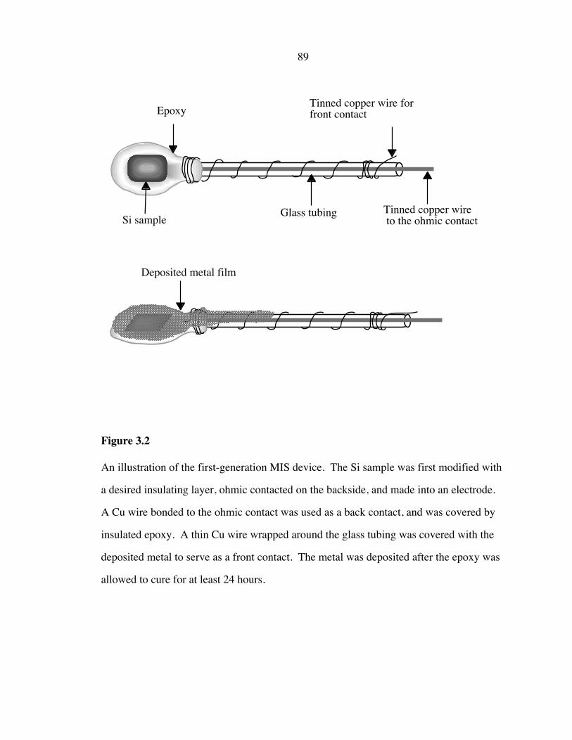
2.4.1. The First-Generation MIS Device
Electrodes were fabricated by attaching a tinned copper wire (22 AWG, Belden)
to the ohmic contact of unmodified Si using electrically conductive silver print (GC
Electronics). As illustrated in Figure 3.2, the wire was encased in glass tubing and the
backside and edges of the electrode were sealed with insulating white epoxy (Epoxy
Patch Kit 1C, Dexter Corp.), leaving only the polished surface of the crystal exposed.
Another thin tinned copper wire was wrapped around the epoxy seal in a close proximity
to the Si and the outside of the glass tubing before the epoxy was completely hardened.
The electrodes were stored in a covered tray for at least 24 hours for the epoxy to cure. A
layer of Ni was then deposited on the front side of electrode, covering the Si and the
epoxy surrounding it, along with the thin tinned copper wire that was situated near the Si.
The front contact was provided by the deposited metal film that electrically connects the
Si surface and the tinned copper wire. A small amount of silver print was painted around
the wire and epoxy to ensure a good electrical connection. Electrode areas were
determined by digitally scanning the electrodes along with a micro ruler, and the exposed
electrode areas were traced and measured using the digitizing software ImageSXM. The
typical exposed electrode areas were 0.05�0.15 cm2.
All electrodes made of modified Si were transferred to a high-vacuum
evaporation chamber (Vacuum Coating Unit LCI-14B, Consolidated Vacuum Corp.) and
evacuated to a pressure of £ 5 ¥ 10-6 Torr. The Ni (99.994%, Alfa AESAR) was
deposited onto the electrodes at a rate of 2�5 Å/s to a thickness of ~450 Å by filament
evaporation. Evaporation rates and film thicknesses were determined by a R. D. Mathis
TM-100 thickness monitor.

86
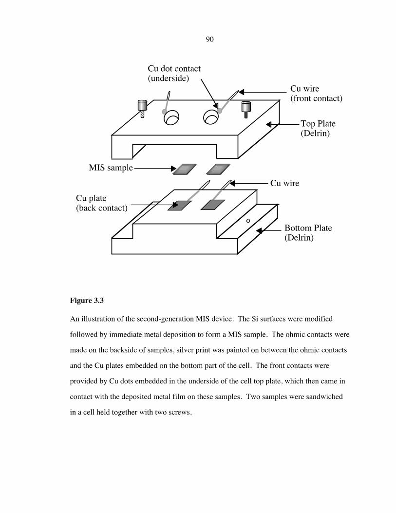
2.4.2. The Second-generation MIS Device
The Si wafers were cut into 5 mm ¥ 5 mm pieces and were modified and
characterized as described. Immediately following the surface derivatization process, the
modified samples were introduced into the evaporator for metal deposition. The
thickness of the deposited metal film was usually 450 Å. Figure 3.3 depicts the cell
assembly of this sandwiched MIS device. Each device could hold two samples at the
same time. Two small Cu plates embedded on the bottom portion of the device provided
the back contacts. The ohmic contacted backside of a sample was bonded to the Cu plate
using silver print. Two thick Cu wires were inserted into the top portion of the device
made of delrin at an angle so that the ends appeared on the surface of the underside near
the two circular openings. The wire ends were cut and polished to the level of the delrin
top plate surface and referred to as Cu dots. When the cell was assembled, the Cu dots
should touch the samples and make electrical contacts with the deposited metal film. The
other ends of these two wires were connected to instruments via alligator clips as front
contacts. The device had two openings for illumination, and a cell holder was used to
position the device so the incident light could hit the surfaces of samples without creating
any shadow. Two screws were necessary to hold together the cell device.
2.4.3. The Third-generation MIS Device
The front contact of the second-generation device was replaced with an indium tin
oxide (ITO)-coated glass obtained from Delta Technology. To avoid short-circuiting, the
ITO-coating was pre-patterned so that the area and the shape of conductive coating match
that of the deposited metal on the Si surface. The design for patterning mask was created
in ClarisDraw version 1.0.4 and was printed out and photographed onto a Kodak mask
plate. At least 30 min prior to the patterning, ITO-coated slides were cleaned in acetone
and 18 MW◊cm H2O, dried in a stream of N2(g), and baked in a 100ûC oven for 30 min.

87
This step served to degrease the slide surface and to eliminate moisture, both could affect
the adhesion of photoresist.
Shipley 1818 photoresist was spin-coated (~30 s) onto the ITO-coated side (cut
into 2.5 mm ¥ 2.5 mm pieces), pre-baked in a 90ûC oven for 20 min, and then exposed to
UV radiation under the patterning mask for 60 s. After immersing the slides in Shipley
CD-30 developer, the UV-exposed part of photoresist was washed off in deionized water.
The slides were blow-dried with N2(g) and post-baked at 90ûC for 15 min. Once the
photoresist pattern was baked onto the ITO coating, the uncovered portion was etched
away in an aqueous solution of 20% HCl (EM Science) and 5% HNO3 (EM Science) at
55ûC for 5�7 min. The ITO-coated slides were rinsed with 18 MW◊cm H2O, and then
immersed in a basic solution or 10% Na2CO3 to neutralize the acid etch. The slides were
again rinsed with 18 MW◊cm H2O and dried under N2(g). The remaining photoresist was
washed off with acetone, followed by another 18 MW◊cm H2O rinse and N2(g) dried. The
ITO pattern could be seen clearly.
The Si samples were cut into 5 mm ¥ 8 mm pieces and were modified and
characterized as described. Immediately following the surface derivatization process, the
modified samples were introduced into the evaporator for metal deposition. The Ni
(99.994%, Alfa AESAR) was deposited onto the electrodes at a rate of 2�5 Å s-1 to a
thickness of ~115 Å or ~500 Å by filament evaporation. The samples used for
measurements in the dark only had thicker metal films to prevent short-circuiting. A
mask was used to limit the area of deposited Ni to a circular shape with an area of 0.1257
cm2, the same size and shape as the patterned ITO front contact. Each cell could hold
two samples at the same time (Figure 3.4).
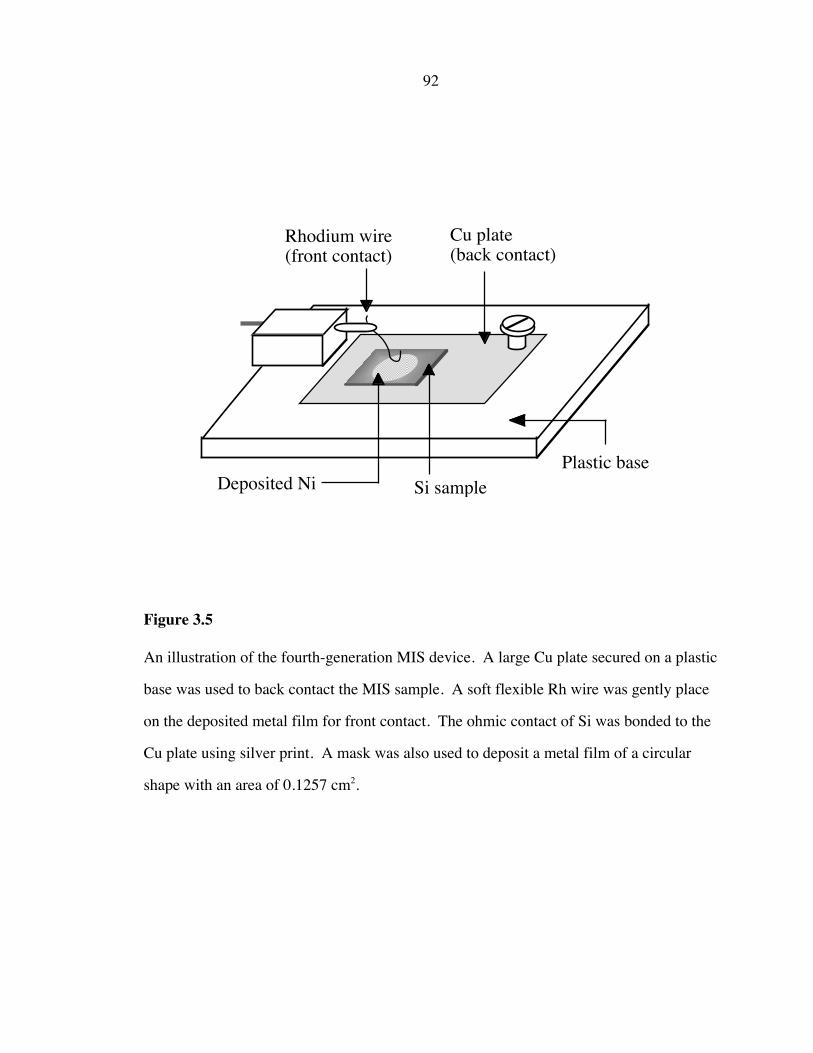
2.4.4. The Fourth-generation MIS Device
The Si samples were modified as described, and 300�500 Å of Ni was deposited
on the modified samples by filament evaporation immediately after the derivatization. A

88
mask was used during the metal deposition to allow a circular shaped metal film of an
area of 0.1257 cm2. The MIS samples were ohmic contacted on the back surface. As
illustrated in Figure 3.5, cell device consisted of a Cu plate that was secured on a plastic
base and a thin Rhodium (Rh) wire held steady by an insulated block was used for
electrical measurements. The backside of a sample was placed on the Cu plate that
served as a back contact with the aid of silver print. The tip of the Rh wire was bent and
gently lowered to the front surface of the MIS sample until an electrical contact was
made. The Rh wire was very thin and relatively flexible, so that it would not penetrate
the metal layer on contact.
89
Si sampleGlass tubing Tinned copper wire
to the ohmic contact
Tinned copper wire for front contactEpoxy
Deposited metal film
Figure 3.2
An illustration of the first-generation MIS device. The Si sample was first modified with
a desired insulating layer, ohmic contacted on the backside, and made into an electrode.
A Cu wire bonded to the ohmic contact was used as a back contact, and was covered by
insulated epoxy. A thin Cu wire wrapped around the glass tubing was covered with the
deposited metal to serve as a front contact. The metal was deposited after the epoxy was
allowed to cure for at least 24 hours.
90
MIS sample
Cu plate (back contact)
Cu wire (front contact)
Top Plate (Delrin)
Cu dot contact (underside)
Cu wire
Bottom Plate (Delrin)
Figure 3.3
An illustration of the second-generation MIS device. The Si surfaces were modified
followed by immediate metal deposition to form a MIS sample. The ohmic contacts were
made on the backside of samples, silver print was painted on between the ohmic contacts
and the Cu plates embedded on the bottom part of the cell. The front contacts were
provided by Cu dots embedded in the underside of the cell top plate, which then came in
contact with the deposited metal film on these samples. Two samples were sandwiched
in a cell held together with two screws.

91
MIS sample
Cu plate(O2-free)
Cu wire
ITO-coated glass
Anti-reflectioncoating on top
Bottom plate
Top plate (Delrin)
Deposited metal film
Figure 3.4
An illustration of the third-generation MIS device. The Si surfaces were modified and
followed by immediate metal deposition with a mask to define the electrode area. The
back contact was made the same way as the second-generation cell. The front contact
was made by using pre-patterned ITO-coated glass to make an electrical contact with the
deposited metal film. The antireflection coating ensured that the illumination intensity
was not greatly affected by the presence of a glass slide. The cell was assembled and
held tight with screws, and could hold two MIS samples for electrical measurements.
92
Rhodium wire(front contact)
Cu plate(back contact)
Deposited Ni Si samplePlastic base
Figure 3.5
An illustration of the fourth-generation MIS device. A large Cu plate secured on a plastic
base was used to back contact the MIS sample. A soft flexible Rh wire was gently place
on the deposited metal film for front contact. The ohmic contact of Si was bonded to the
Cu plate using silver print. A mask was also used to deposit a metal film of a circular
shape with an area of 0.1257 cm2.
93
2.5. Surface Characterization
All surfaces were characterized by x-ray photoelectron spectroscopy (XPS). The
experiments were conducted in an M-probe surface spectrometer (VG Instrument)
pumped by a CTI Cryogenics-8 cryo pump. Samples could be introduced into the UHV
system using either the atmospheric load lock or the glove box load lock. The
atmospheric load lock was pumped by a Varian model V80 turbo pump and a Varian
model SD-300 mechanical pump, and allowed samples to be introduced into the UHV
from air. The glove box load lock was pumped by a Varian model V200 turbo pump and
a Varian model SD-300 mechanical pump, and enabled samples to be transferred into the
UHV through a gate valve that opened to the N2(g)-purged glove box. These load locks
were brought to the atmospheric pressure by back-filling with N2(g), and can be pumped
down to approximately 10�7 Torr in about 10 min. Samples were mounted on a stainless
steel or aluminum stub with screws.
The XPS chamber was maintained at a base pressure of less than 5 ¥ 10�10 Torr,
although the operating pressure was 5 ¥ 10�9 to 2 ¥ 10�8 Torr. Monochromatic Al Ka x-
rays (hv = 1486.6 eV) incident at 35° from the sample surface were used to excite
electrons from the sample, while the emitted electrons were collected by a hemispherical
analyzer at a take-off angle of 35∞ from the plane of the sample surface. Data collection
and analysis were done with the M-probe package software version 3.4. Survey scans
were collected in the scanned mode with an elliptical spot of dimensions 800 µm ¥ 1200
µm incident on the sample surface. The high-resolution scans were recorded in an
unscanned mode with the same spot size. A typical XPS characterization of a surface
consisted of one survey scan from 0�700 eV binding energy and a high resolution scan of
the Si 2p region (97.57�104.59 eV binding energies).

94
2.6. Electrical Measurements
Electrical characterization of MIS samples was performed using a two-electrode
configuration with the ohmic contact to the back of the Si as the working electrode and
the metal contact on the front of the electrode as the counter/reference electrode. The
electrodes and cell devices were positioned so that incident light arrived normal to the
sample surface.
Current density vs. potential (J–E) measurements were performed using a
Solartron Model 1287 potentiostat or an EG&G Princeton Applied Research (PAR)
Model 173 potentiostat/galvanostat equipped with an EG&G PAR Model 175 universal
programmer. When EG&G PAR Model 173 potentiostat/galvanostat was used, traces
were recorded on a Houston Instruments Omnigraphic 2000 chart recorder. All curves
were recorded at a scan rate of 100 mV s-1. Light intensities were controlled by the use of
a 300 W ENH-type tungsten-halogen bulb in conjunction with neutral density filters
(ND-50, Hoya Optics). A 10 cm path-length flowing water column was used to filter out
the infrared portion of the lamp output and thereby prevent excess heating of the sample.
The photoresponse experiments involved collecting the photocurrent density (Jph)
and the open-circuit voltage (Voc) values at different illumination intensities. Direct
measurements of Voc and Jph were taken by reading the appropriate quantities through a
Fluke 27 digital multimeter. The reverse saturation current (J0) and the diode quality
factors (g) of CnH2n+1-terminated Si (n = 2�8) /Ni junctions were obtained.
The current-voltage properties for most semiconductor diodes are found to obey
the equation:23
J JqV
kT=
-Ê
ËÁ
�
¯� -
È
ÎÍ
ù
ûú0 1exp
g(3.2)
95
where J0 = A**T2[exp(-qfb/kT)], q is the charge on an electron, V is the applied potential, g
is the diode quality factor, k is Boltzmann�s constant, T is the absolute temperature, and
A** is the modified Richardson�s constant (for n-Si, A** ª 120 A/cm2◊K2).24 Dark J–E
measurements allow the preparation of a plot of lnJ vs. V, which should give a linear
relationship of the form:
ln lnJqV
kTJª
-+
g0 (3.3)
where J0 and g can be extracted from the data. When the diode is under illumination, the
current can be described by adding the current from photogenerated carriers to the dark
current.25,26 Equation 3.11 can be modified to describe the J–E relationship under
illumination:
J J JqV
kT= -
-Ê
ËÁ
�
¯� -
È
ÎÍ
ù
ûúph 0 1exp
g(3.4)
At open circuit (J = 0), Equation 3.10 is rearranged to yield the following expression:27
VkT
q
J
Jocph@
Ê
ËÁ
�
¯�
gln
0
for Jph >> J0 (3.5)
Following this equation, a photoresponse experiment can also provide an experimental
value for both g and J0.
Since most MS diodes are dominated by thermionic emission (i.e., g = 1),26 the
barrier heights can be calculated from the following:
fb =Ê
ËÁ
�
¯�
kT
q
A T
Jln
** 2
0
(3.6)

96
By using metals with different work functions to construct equivalent MS and MIS
diodes, a comparison of the two measured barrier heights will allow verification of the
effectiveness of the interfacial alkyl layer.

97
3. Results
3.1. Surface Modification
The surface modification process was monitored and verified using XPS. Figure
3.6 displays the XP spectra obtained at each step of the surface modification process. A
successful etching procedure produced an H-terminated Si surface with a clean spectrum
showing large Si 2p and Si 2s peaks at 99 eV and 149 eV binding energies. The smaller
peaks present at successive intervals of 17.5 eV binding energy higher than the main Si
2p and 2s peaks were plasmon loss peaks, and were characteristic of Si surfaces.28,29
Small signals due to adventitious carbon and oxygen were often observed at 284.6 eV (C
1s) and 532 eV (O 1s). The presence of adventitious carbonaceous material on the silicon
surface was a result of wet chemical etching and subsequent brief handling of samples in
air.30,31 The lack of signal in the 101 to 104 eV region of the Si 2p high-resolution XP
spectra collected with each survey scans suggested that the oxygen signal observed in
survey spectra was not due to silicon oxide.
Figure 3.6b shows the representative spectrum of a chlorinated Si surface.
Addition peaks were observed at 270 eV and 200 eV binding energies, which correspond
to Cl 2s and Cl 2p peaks.16 The subsequent Grignard reaction displaced the surface
chlorine atoms, and the alkylated surface was confirmed by the disappearance of the Cl
peaks and the concomitant increase in magnitude of the C 1s peak in the XP survey
spectrum (Figure 3.6c). For alkyl chain lengths of up to 8 carbons, the modification
process was straightforward without complication. However, the attempt to attach decyl
groups to the Si surfaces resulted in significant oxide growth during the Grignard
reaction.

98
Figure 3.6
XP survey spectra of (a) H-terminated Si, (b) Cl-terminated Si, (c) C3-terminated Si, (d)
C6-terminated Si, and (e) C10-terminated Si. All spectra were normalized relative to the
intensity of the Si 2p peak. The small C 1s and O 1s peak in (a) were due to
advantageous C and O as a result of wet chemical etching and brief handling in air.
Spectra (c)�(e) display the relative intensities of C 1s peak for 3 Si surfaces modified
with alkyl chains of different lengths. The C 1s peak intensity generally increases as
longer alkyl chains were attached.

99
0100200300400500600700
Inte
nsit
y (a
.u.)
Binding Energy (eV)
Si 2pSi 2s
C 1s
O 1s
(a)
(b)
(d)
(c)
(e)
Cl 2p
Cl 2s

100
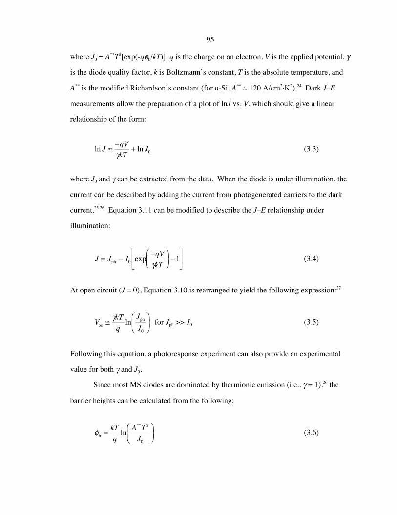
3.2. The J–E Behaviors of MIS Diodes
Figure 3.7 display the J–E behaviors of an H-terminated Si/Ni contact and a C3H7-
terminated Si/Ni contact, respectively. The measurements were performed using the
first-generation device. The introduction of the covalently attached propyl layer showed
significant lowering of the J0 and slight increases in the Voc values at similar Jph. This
provided promising result for the concept of making MIS devices using alkyl chains as
insulating layers. However, reproducibility in J–E behaviors was not achieved, as J–E
curves looked somewhat different from one electrode to another.
The second-generation device did not work very well. The Cu dots did not make
good enough electrical contacts with the deposited Ni film. The cell resistance was
measured to be as high as 350 W. The cell resistance was lowered when silver print was
used to aid the front electrical contact, however, due to the small dimension of the Cu
dots, the use of silver print was somewhat difficult. In many cases the silver print
dripped down the side of the sample and short-circuited the front and the back contact.
The device was modified to incorporate the use of highly conductive ITO-coated
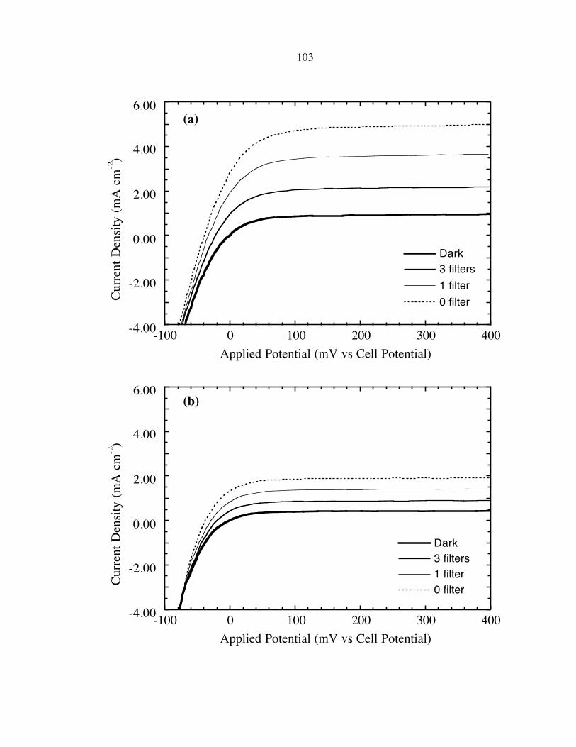
slides to make front contacts with MIS samples. This third-generation cell device
certainly provided more reliable front contacts. The cell resistance was typically under
60 W. Although still suffered from irreproducibility between samples, a set of J�E
behavior data was collected using a series of CnH2n+2-terminated Si (n = 2, 4, 6, and 8)
modified at the same time along with an H-terminated Si. A thin layer of Ni (114 Å) was
deposited on these samples at a rate of £2.0 Å s-1. Figure 3.8 displays the J�E properties
of these MIS junctions in the dark. The Si-H/Ni junction had a large anodic current at
reverse biases indicating a very week diode behavior due to a large J0. With an ethyl
layer in between the Si and the Ni, the J�E curve improved significantly, although still
exhibited a large reverse saturation current. When the J�E behaviors of C4H9-, C6H13-,
and C8H17-terminated Si/Ni junctions were plotted together with H- and C2H5-terminated

101
Si/Ni junctions, it was clear that the insulating layers were capable of lowering the J0 and
also resulted in larger Voc values.
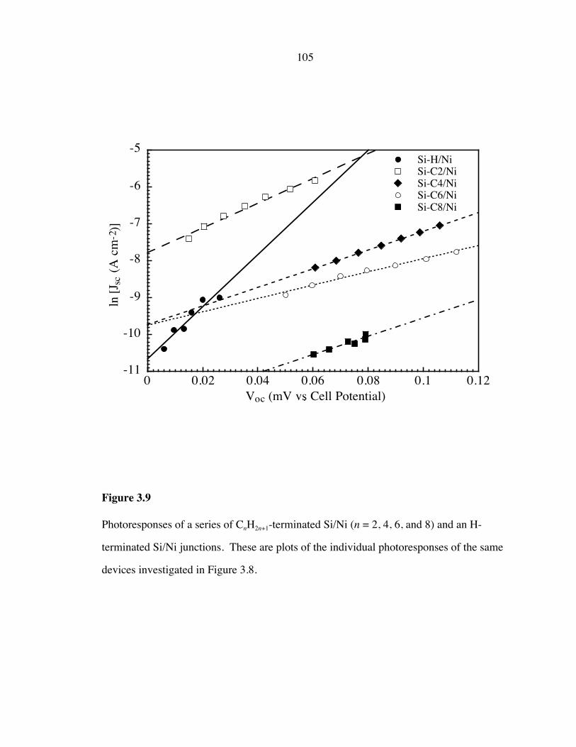
The photoresponses of these MIS devices were also measured at several different
illumination intensities. The lnJsc vs. Voc data were plotted in Figure 3.9. Again, the
results showed the same effect observed in earlier J–E experiments. The C8H17-
terminated Si/Ni junction was the best choice of all devices tested, with a lower J0 and
higher Voc value compare to the other junctions tested. Because the J–E behaviors of both
Si-H and Si-C2H5/Ni junctions did not follow the diode equation, and anodic currents did
not level out in the reverse bias region studied, a quantitative calculation was not
possible. A time dependence of several C8H17-terminated Si/Ni junctions J–E behaviors
was also performed. The samples were left in the air for 3 days and the J–E curve of
each device was collected every 24 hours. As depicted in Figure 3.10, this junction was
not air stable and the J–E characteristics deteriorate quickly to show large resistance in
the forward bias region.
Since the third-generation device still did not allow reproducible data to be
collected, the fourth-generation device that was very similar to the device used for prior
MIS study in our laboratory was tested.15 A larger number of the same surface was made
at the same time to insure the same quality control. The attempts to achieve reproducible
J–E behaviors for several types of surfaces were unsuccessful.

102
Figure 3.7
J–E behaviors of (a) H-terminated and (b) C3H7-terminated Si in contact with 450 Å of
Ni. The plots were collected using the first-generation cell device. The plots were
collected at a scan rate of 100 mV s-1. A significant lowering of the anodic currents at
reverse biases suggested that the junction recombination current was lowered when an
insulating layer was introduced between the Si and the contacting Ni. The illumination
intensities were kept the same for both devices.
103
-4.00
-2.00
0.00
2.00
4.00
6.00
-100 0 100 200 300 400
Dark3 filters
1 filter
0 filterCur
rent
Den
sity
(m
A c
m-2
)
Applied Potential (mV vs Cell Potential)
-4.00
-2.00
0.00
2.00
4.00
6.00
-100 0 100 200 300 400
Dark3 filters1 filter0 filter
Cur
rent
Den
sity
(m
A c
m-2
)
Applied Potential (mV vs Cell Potential)
(a)
(b)
.
.

104
-0.01
-0.005
0
0.005
0.01
-0.4 -0.2 0 0.2 0.4 0.6
Si-H/NiSi-C2/NiSi-C4/NiSi-C6/NiSi-C8/Ni
Cur
rent
Den
sity
(A
cm
-2)
Applied Potential (V vs Cell Potential)
Figure 3.8
J–E behaviors of a series of CnH2n+1-terminated Si/Ni (n = 2, 4, 6, and 8) and an H-
terminated Si/Ni junctions in the dark. The data show the dependence of the MIS
junction J–E behavior on the alkyl chain length. The MIS junction with the longest
insulator chain length exhibited the lowest anodic current at reserve biases. The MIS
diode constructed using a thicker insulator was more resistive at forward bias.
.
105
-11
-10
-9
-8
-7
-6
-5
0 0.02 0.04 0.06 0.08 0.1 0.12
Si-H/NiSi-C2/NiSi-C4/NiSi-C6/NiSi-C8/Ni
ln [
J sc
(A c
m-2
)]
Voc (mV vs Cell Potential)
Figure 3.9
Photoresponses of a series of CnH2n+1-terminated Si/Ni (n = 2, 4, 6, and 8) and an H-
terminated Si/Ni junctions. These are plots of the individual photoresponses of the same
devices investigated in Figure 3.8.
.

106
-1.00
-0.80
-0.60
-0.40
-0.20
0.00
0.20
-200 -100 0 100 200 300
Initial1 day in Air2 day in Air3 day in Air
Cur
rent
Den
sity
(A
cm
-2)
Applied Potential (mV vs Cell Potential)
Figure 3.10
Time-dependent J–E behavior of a C8H17-terminated Si/Ni junction in the dark. The MIS
device constructed was not stable in air. The device resistance increased during the
course of 3 days, which suggested the possibility of unfavorable interfacial reaction.
.

107
4. Discussions
The XPS data confirmed that the two-step chlorination/alkylation method yielded
reproducible alkyl overlayer on a Si(111) surfaces. The model suggested that the best
possible coverage for an alkylated Si is a half-monolayer coverage (as a 2 ¥ 1 unit cell),
with the exception of methylated surface, which could exhibit one-monolayer coverage.
Since the area of the 2 ¥ 1 unit cell on Si(111) surface is significantly larger than the area
required for an alkyl chain in a tightly packed environment, the alkyl overlayer could be
quite porous.22 Although the methyl overlayer could provide a better coverage, it was too
thin to alter the electrical properties of an H-terminated Si/Ni contact. In fact, the data
showed that there was no significant effect when an alkyl chain of shorter than 3 carbons
was used as the insulating layer. A longer alkyl chain, on the other hand, could tilt to
make the overlayer surface less porous and provide a necessary barrier against silicide
formation. However, the possible introduction of an additional series resistance was
observed in J–E plots.
The irreproducibility problem could arise from the junction formation process
rather than the design of devices for measurements. Thermal evaporation of Ni requires
relatively high temperature, and the organic layers on these samples could disintegrate or
get damaged under excess heat. The dust could also introduce problems during
evaporation and result in inconsistent interfaces. If the metal was deposited in the pin
holes or if the hot metal burnt through the organic insulator, the MIS junctions could
produce unreliable data, making it difficult to analyze the experimental results
quantitatively.
As an alternative to the porosity problem, linear fluorocarbon chains can be used
to derivatize the Si surface instead of alkyl chains. The larger head groups of
fluorocarbon chains could serve as a blocking layer and might result in a much more

108
chemically impenetrable coverage, therefore a better barrier against metal penetration in a
MIS contact.
Different metal deposition methods can also be investigated. Electroless
deposition of gold or nickel onto GaP has been reported to yield almost ideal Schottky
diodes.32 Palladium and copper contacts to Si have also been made using an electroless
process.33,34 Metal-binding agents such as thiols can be incorporated into the monolayer
head group, which can in turn bind colloidal Au and Pt.35,36 Electrodeposition can also be
adapted to plate a metal layer on the alkyl monolayer-Si substrate with a well controlled
thickness.37,38 There are however other concerns for liquid phase deposition. It is unclear
as to how the trapped liquid molecules might affect the electrical properties of the
junction. Since the alkyl layer is somewhat porous, the liquid could actually come in
contact with Si substrate and either induce oxide growth or allow the metal deposition to
occur directly on the Si surface where it�s not covered. Electroplating current would
prefer to go through the areas with the least resistance, and this could mean that it is
easier for metal plating to occur at the sites of pin holes, which again decreases the
effectiveness of insulating layer.
Another approach for the fabrication of MIS diodes is mass production of the
same junction. By making large batches of junctions for measurements, it would be
possible to recognize and discard unreliable data from each set of measurement. This
could be achieved by modifying the surfaces of large wafers instead of smaller size
samples, followed by depositing metal dots or islands to form a large number of junctions
on each modified wafer. Since it is easier to have a smaller area of modified surface to
be free of defect than the whole sample surface, those metal dots that were deposited on a
region that has no pin hole would be able to provide reliable data for junction
characterizations.
Once an effective alkyl monolayer is obtained, different metals should be
deposited onto both H-terminated Si and derivatized Si to make equivalent MS and MIS

109
diodes. In an order of decreasing metal work functions, metals that can be used are Pt,
Pd, Au, Rh, Ni, Co, Cu, Cr, Al, and Ag. Pt, Pd, and Au should yield large barrier heights
at unpinned metal/n-type Si junctions, while Ag, Al, and Cr/n-Si interfaces should
produce a Voc ª 0 due to theoretically low barrier heights.

110
5. Summary
Several different chain lengths of alkanes, from methyl to octyl groups, have been
successfully attached to the n-Si(111) surface using a two-step chlorination/alkylation
method. Contacting Ni layers of thicknesses ranging from 115 Å to 500 Å have been
thermally evaporated onto both freshly etched H-terminated and alkyl-terminated Si, and
the J–E behaviors of these resulting junctions have been investigated. Introduction of a
monolayer with a chain length longer than 4 carbons between the Ni and the Si was
shown to consistently lower the value of J0 while an increase in the values of Voc were
observed. A general trend of an increased effectiveness was shown for longer alkyl
chains, but the thicker films also introduced larger cell resistances. Although
reproducibility of the MIS J–E properties could not be achieved despite the use of several
different cell devices, some suggestions were presented for possible future work.
6. Acknowledgments
I thank Reynold Johnson in the Department of Applied Physics for assisting with
the photoresist patterning.

111
7. References
(1) Braun, F. Ann. Phys. Chem. 1874, 153, 556.
(2) Sharma, B. L., Ed. Metal-Semiconductor Schottky Barrier Junctions and Their
Applications; Plenum: New York, 1984.
(3) Schottky, W.; Stromer, R.; Waibel, F. Hochfrequenztechnik 1931, 37, 162.
(4) Schottky, W. Naturwissenschaften 1938, 26, 843.
(5) Mott, N. F. Proc. Camb. Phil. Soc. 1938, 34, 568.
(6) McGill, T. C. J. Vac. Sci. Technol. 1974, 11, 935.
(7) Bardeen, J. Phys. Rev. 1947, 71, 717.
(8) Heine, V. Phys. Rev. A 1965, 138, 1689.
(9) Schmid, P. E.; Ho, P. S.; Foll, H.; Tan, T. Y. Phys. Rev. B-Condens Matter 1983,
28, 4593.
(10) Schmid, P. E. Helv. Phys. Acta 1985, 58, 371.
(11) Rhoderick, E. H.; Williams, R. H. Metal-Semiconductor Contacts; 2nd ed.;
Oxford University Press: New York, 1988.
(12) Ottaviani, G.; Tu, K. N.; Mayer, J. W. Phys. Rev. Lett. 1980, 44, 284.
(13) Freeouf, J. L.; Rubloff, P. S.; Ho, P. S.; Kuan, T. S. J. Vac. Sci. Technol. 1980,
17, 916.
(14) Andrews, J. M.; Phillips, J. C. Phys. Rev. Lett. 1975, 35, 56.
(15) Rosenblum, M. D. Ph. D., Stanford University, 1988.
(16) Bansal, A.; Li, X.; Lauermann, I.; Lewis, N. S.; Yi, S. I.; Weinberg, W. H. J. Am.
Chem. Soc. 1996, 118, 7225.
(17) Linford, M. R.; Chidsey, C. E. D. J. Am. Chem. Soc. 1993, 115, 12631.
(18) Linford, M. R.; Fenter, P.; Eisenberger, P. M.; Chidsey, C. E. D. J. Am. Chem.
Soc. 1995, 117, 3145.
(19) Higashi, G. S.; Chabal, Y. J.; Trucks, G. W.; Raghavachari, K. Appl. Phys. Lett.
1990, 56, 656.
(20) Wyman, D. P.; Wang, J. Y. C.; Freeman, W. R. J. Org. Chem. 1963, 28, 3173.
(21) Hassler, K.; Koll, W. J. Organomet. Chem. 1995, 487, 223.
(22) Bansal, A. Ph. D., California Institute of Technology, 1997.
(23) Sze, S. M. The Physics of Semiconductor Devices; 2nd ed.; Wiley: New York,
1981.
(24) Andrews, J. M.; Lepselter, M. P. Solid State Elec. 1970, 13, 1011.

112
(25) Fonash, S. J. Solar Cell Device Physics; Academic: New York, 1981.
(26) Fahrenbruch, A. L.; Bube, R. H. Fundamentals of Solar Cells: Photovoltaic Solar
Energy Conversion; Academic: New York, 1983.
(27) Kumar, A.; Wilisch, W. C. A.; Lewis, N. S. CRC Critical Rev. 1993, 18, 327.
(28) Stinespring, C. D.; Wormhoudt, J. C. J. Appl. Phys. 1989, 65, 1733.
(29) Cheng, K. L. Japan. J. Appl. Phys. 1995, 34, 5527.
(30) Tufts, B. J.; Kumar, A.; Bansal, A.; Lewis, N. S. J. Phys. Chem. 1992, 96, 4581.
(31) Mende, G.; Finster, J.; Flamm, D.; Schulze, D. Surf. Sci. 1983, 128, 169.
(32) Gol'dberg, Y. A.; Posse, E. A.; Tsarenkov, B. V. Electron. Lett. 1971, 7, 601.
(33) Datta, A. K.; Ghosh, K.; Mitra, R. N.; Daw, A. N. Solid-St. Electron. 1980, 23,
99.
(34) Datta, A. K.; Ghosh, K.; Chowdhury, N. K. D.; Daw, A. N. Solid-St. Electron.
1980, 23, 905.
(35) Natan, M. J.; Thackeray, J. W.; Wrighton, M. S. J. Phys. Chem. 1986, 90, 4089.
(36) Freeman, R. G.; Grabar, K. C.; Allison, K. J.; Bright, R. M.; Davis, J. A.;Natan, M. J. Science 1995, 267, 1629.
(37) Bocking, C.; Christie, I. R. Inter. Sci. Rev. 1992, 17, 239.
(38) Searson, P. C. Solar Energ Mater Solar Cells 1992, 27, 377.