chapter 3 power quality and dynamic voltage restorer...
TRANSCRIPT
CHAPTER 3
POWER QUALITY AND DYNAMIC VOLTAGE RESTORER (DVR)
3.1 INTRODUCTION TO POWER QUALITY
Power quality has become major concern to both electric utilities
and customers. In many countries, the effects of lack of power quality
have been resulting in wastage of several billions of dollars every year.
This is due to carelessness of most industries in not upgrading their
plants which result in very high cost due to loss of products, loss of
production time, clean up and recalibration of the process. The use of
complexity and sensitivity of new technologies in electric equipments is
one of the major causes of power quality problems such as voltage
disturbances on the supply network. Power electronic equipments are
more sensitive to voltage disturbances and leads to large growth of
voltage disturbances. It is difficult to detect the sources leading to
power quality problems. Factors for the causes of most power quality
problems are beyond the control of utilities and can never be totally
eliminated. Some of the sources of power quality problems in order of
frequency of occurrence are:
1. User loads
2. User electrical system and grounding
3. Weather related such as lightening, wind and rain
4. Utility distribution system
5. Utility transmission system

6. utility generation system
Power quality review is a complex subject and involves aspects such
as power system, equipment modeling, power quality event mitigation
and optimization and data analysis. The basic knowledge of the
different power system disturbances is important in order to determine
the events and causes of equipment failure as well as to apply
mitigation measures more effectively. Power system disturbances are
dominated by voltage quality and harmonics.
3.2 Voltage Quality
The control and design are the two constraints of DVR which are
affected by voltage quality. The DVR performance depends on the
voltage quality at the location DVR is inserted. Voltage quality includes
sags, swells, interruptions and harmonics.
3.2.1 Voltage sags
Voltage sags are in many references stated as the most important
and costly power quality problems and, because of high risk of tripping
devices and a relative frequent occurrence. Voltage sags have been
treated in many papers for instance. Voltage sags are categorized as
symmetrical and unsymmetrical.
3.2.1.1) Symmetrical voltage sags
Voltage sags are usually caused b short –circuit current into fault
and a simplified model is illustrated in fig 3.2. Magnitude and phase of
the voltage sag at the point of common coupling (PCC) are determined
by the fault and supply impedances, using the following eqn.3.1:
Zfault
V =EZ +Z
fault supply
sag (3.1)
By the impedance considerations the reduced magnitude and in
some cases a phase jump can be estimated. Fig 3.2 illustrates the used
definitions of the voltage at the PCC with Vsag as the voltage during the
sag and Φsag is the phase jump at PCC. Simple symmetrical voltage sag
can be characterized by the following three parameters
Voltage during sag (Vsag)
Sag duration (tsag)
Phase jump (Фsag)
Fig 3.1: Simplified ciruit for voltage sag calculation
Fig 3.2: Vector diagram of various voltages during sag
The definition of voltage sag with phasors can be stated as:
V = V -Vpresag missingsag (3.2)
E Zf
Load
PCC
Zs
Fault
Supply
Vsag
Vpresag
Vmissing
Фsag

As per the definition, the voltage sag is the voltage at PCC during
the voltage sag and can be calculated as pre-sag voltage (often the rated
voltage) subtracted the missing voltage. In order to have full
compensating, the DVR must inject the missing voltage. If the voltage
sag is severe, Vsag is low and shallow voltage sag is characterized as
high Vsag value.
3.2.1.2) Non-symmetrical voltage sags
Usually the large portion of the voltage sag will be non-symmetrical
in nature. These non-symmetrical natures have a considerable impact
on the design and control of DVR and voltage sag distribution could
justify the design of the DVR for non-symmetrical voltage sags and
therefore focus performance evaluation on the compensation of non-
symmetrical sags.
The voltage sags are caused by different kinds of faults in the grid.
The faults can be categorized as:
1. Three-phase faults
2. Three-phase faults with ground connection
3. Two-phase faults
4. Two-phase faults with ground connection
5. Single-phase faults
In direct or effective grounded systems (3-5) can lead to non-
symmetrical voltage sag and in isolated or high impedance grounded
system (3-4) can lead to non-symmetrical voltage sag. The propagation
through transformers and grounding used at each voltage level is
essential for the propagation of the voltage sags associated with faults.

Non-symmetrical voltage sags very often include a phase shift of two
phases and depending on the circumstances, the voltage phasors come
closer or more separate. The phase-shift, which is very different from
the phase jump from symmetrical voltage sag, must be detected and
compensated by the DVR to restore the load voltages. The magnitude to
be injected by the dynamic voltage restorer is important, because the
DVR has a finite voltage rating and it sets a limit for the type of non-
symmetrical sags, which can be compensated. For some DVR topologies
the line voltage values are of greater interest. The positive sequence
component is also useful for evaluating the expected power drain for
non-symmetrical voltage sag, because for symmetrical load currents, on
the injection of positive sequence results in a power drain for the DVR
storage.
3.2.2 Voltage Interruptions
Voltage interruptions are usually caused by different types of faults
e.g. malfunction of protection equipment or lightening. Sometimes,
without redundancy, fault often leads to long interruption, which
requires manual intervention. Short interruptions are often caused by
automatic reclosing after fault. Short interruptions below three minutes
are normally considered a voltage quality problem. Interruptions are a
severe power quality problem. Occurrence of voltage interruptions is
very rare because of redundancy and high maintenance of the grid
especially in wide range of industrial countries. A correlation can be
found between interruptions and voltage sags. Taking measures to
decrease the number of interruptions may increase the number of

voltage sags. For instance by having a meshed distribution system
(high redundancy) the number of interruptions goes down, but the
voltage sags can occur more frequently and be more severe.
3.2.3 Voltage Harmonics
Harmonics are treated as non fundamental voltage signals often
appear at all levels in the electrical system. With reference to DVR, the
harmonic content of the voltage before and after the DVR operation has
major interest. Before the DVR, background distortion level (during no-
load conditions) can be measured and the level of distortion may
influence the control of the DVR. The DVR can inject some harmonics
in addition to background harmonics gives the resulting load voltage
harmonics. This resulting load voltage distortion is an important
evaluation parameter of the DVR performance. Sources to the distortion
of the load voltages vary and the three main sources are:
Background voltage harmonics: Background harmonics can
easily be transferred to the load voltage side. During voltage
injection harmonics from background distortion can be amplified
or damped in the DVR control system. A supply voltage with high
harmonic content can complicate the synchronization to the
supply and interface with the DVR control.
Harmonics injected by the DVR: The THD of the injected series
voltage depends on the DVR hardware (converter topology,
switching frequency, modulation method, modulation index and
filtering). Non-linear effects in the converter can even be a pure
fundamental reference voltage injects harmonics, caused by non-

linear effects in the DVR such as dead time, transistor and diode
voltage drop.
Non-linear load currents: A non-linear load currents distorts the
load voltage, which depends on the strength of the grid, the
inserted DVR and the resulting impedance seen by load. This will
include impedance in the DVR and the grid.
The voltage distortion Vsag can be calculated by a summation of
harmonic components, according to:
2
2sagV V
hh
(3.3)
And the total harmonic distortion (THD) in percent can be calculated
by:
VV = 100%
THD%V
1
sag (3.4)
The DVR has the potential of improving the load voltage with
respect to harmonic distortion, which means both compensate for
background harmonics and to compensate for the distorted load voltage
caused by a distorted load current. This type of control is often termed
as harmonic blocking control or series harmonic filtering.
3.2.4 Non-symmetrical voltages
In a three phase system the degree of symmetry is very important
for a large group of three-phase loads. For a DVR non-symmetry
implies hardware and control to be able to detect and correct the
unbalanced supply and load voltages. The degree of symmetry is main
performance criteria, which can be used to evaluate the DVR.
In the analysis of three-phase systems the decomposition to
symmetrical components is useful. Equation 3.5 shows the
transformation from phase phasor values to symmetrical components.
21 a aV Vd a1 2
V = 1 a a Vq b3
1 1 1 VV co
(3.5)
The degree of symmetry is often evaluated as the negative sequence
component divided by the positive sequence component. According to:
VqV = 100%
non-symmetric %V
d
(3.6)
It is important to distinguish the non-symmetry from the four different
sources:
Background non-symmetry: Caused by other loads and can be a
relative permanent condition, which can interface with the DVR
control and make the load voltages non-symmetrical.
Non-symmetrical loads: A high non-symmetrical load can,
because of the voltage drop across the DVR and the supply, lead
to non-symmetrical load voltages.
Non symmetrical voltage sag: Short duration non-symmetry
caused by a non symmetrical fault incident in the grid.
Non-symmetry generated by the DVR: A DVR inserted to remove
symmetrical and non-symmetrical voltage sags, but in some

cases the DVR may increase the non-symmetry by voltage
injection or by the voltage drop caused by non-symmetrical load
currents.
3.3 Series Voltage Controller [Dynamic Voltage Restorer, (DVR)]
The series controllers for control of the fundamental voltage are
termed as a series connected PWM regulator in, a static series regulator
in and, but mostly the devices are termed dynamic voltage restorers. If
the device only injects reactive power the device can be termed as series
var compensators.
Taking the same simplified model of supply and load, but now with a
series controller inserted to support the load. A 0.5 pu voltage sag can
by a series device be restored by a 0.5 pu DVR and only 0.5pu of the
energy absorbed by the load has to be supplied by the DVR. The supply
continues to be connected and no resynchronization is necessary as it
is the case with a shunt connected converter.
Fig 3.3: Circuit diagram of a system with series controller,

The series voltage controller is connected in series with the
protected load as shown in figure 3.3. Usually the connection is made
via a transformer, but configurations with direct connection via power
electronics also exist. The resulting voltage at the load bus bar equals
the sum of the grid voltage and the injected voltage from the DVR. The
converter generates the reactive power needed while the active power is
taken from the energy storage. The energy storage can be different
depending on the needs of compensating. The DVR often has
limitations on the depth and duration of the voltage sag that it can
compensate. Therefore right sized has to be used in order to achieve the
desired protection. Options available for energy storage during voltage
sags are conventional capacitors for very short durations but deep,
batteries for longer but less severe magnitude drops and super
capacitors in between. There are also other combinations and
configurations possible.
There are configurations, which can work without any energy
storage, and they inject a lagging voltage with the load current. There
are also different approaches on what to inject to obtain the most
powerful solution. The main advantage with this method is that a single
DVR can be installed to protect the whole plant (a few MVA) as well as
single loads. Because of the fast switches, usually IGBT’s, voltage
compensation can be achieved in less than half a cycle. Disadvantages
are that it is relatively expensive and it only mitigates voltage sags from
outside the site. The cost of a DVR mainly depends on the power rating
and the energy storage capacity.
Fig.3.4: Configuration for a DVR.
3.3.1 Principle of DVR
Dynamic voltage restorer (DVR) protects the load from voltage
disturbances. DVR maintains the load voltage at a predetermined level
during any source voltage abnormal conditions such as voltage
sags/swells or distortion. The working principle of the DVR can be
explained through the fig 3.4. Under normal operating conditions, let
the three phase voltage phasors Va1, Vb1 and Vc1. During abnormal
conditions, the phase voltage vectors may be altered to Va2, Vb2 and
Vc2. DVR does not supply any real power in the steady state. This
implies that the phase angle difference between DVR voltage phasor
and current phasor must be 900 in the steady state.
DVR injects the required compensating voltage through
transformer. The transformer is connected in series to the load. DVR
operates only during the abnormal conditions and remains idle during
normal operating conditions. During operation, DVR has a capability to
supply and absorb active and reactive power. Dynamic voltage restorer
corrects the load voltage by supplying reactive power generated
internally on the occasion of small fault. DVR develops active power

when it is required to balance larger faults. It requires dc energy device
to develop the active power. Usually, dc capacitor banks are used as
the dc energy storage device. Most often caused voltage disturbances
are voltage sags as they can cause load tripping. Dynamic voltage
restorer (DVR) is a series controller connected in series to the load. DVR
injects voltage in series to the load through the injection transformer
and voltage source converter. The injecting transformer injects the
required voltage vector (magnitude and angle) which adds to the source
voltage to restore the load voltage to pre-abnormal condition. The
components of DVR are:
a) Energy Storage: usually batteries are used to provide the required
energy for compensation of load voltage during abnormal conditions. In
online monitoring and conditioning systems, required energy for
compensation is drawn from supply line feeder through a rectifier and a
capacitor. In low power applications, photovoltaic cells can also provide
energy.
b) Inverter circuit: Since the loads in distribution system operate with
ac power supply, inverter is required to invert the dc power from the
energy storage into ac power. Usually for normal three phase supply,
three phase voltage source inverter is used. Three phase VSI cannot
control the output voltage instead only transform the dc signal to
corresponding ac with same magnitude. Hence requires large energy
storage for high voltage injection. Moreover, voltage source inverter
output waveform shape is step waveform (treated as highly harmonic

content waveform) and hence requires a filter at the output of the
inverter to modify the step output into sinusoidal.
c) Series injection transformers: Three single phase injection
transformers are used to inject the voltage at the load end. Usually 1:1
ratio is used, but if required step up transformer can also be used. The
injection transformers are provided with suitable MVA rating, the
primary winding voltage and current ratings, short circuit impedance
values.
d) Filter Unit: Since the semiconductor devices exhibit non-linear
characteristics resulting in distorted waveforms associated with high
frequency harmonics at the inverter output. Hence to minimize the
harmonics, a harmonic filtering unit is required. In turn the filtering
unit can cause voltage drop and phase shift in the fundamental
component of the inverter output. To overcome this problem, multilevel
topology can be used in voltage source inverter which has double
impact in reducing filter size and energy storage requirement
simultaneously.
e) Controller and auxiliary circuits: By-pass switches, breakers and
protection relays are some auxiliaries to the Dynamic Voltage Restorer
(DVR) block. In addition to all these, PWM controller is required to
generate pulses to the inverter in accordance to the abnormality in load
voltage. Most often PI controller is used. When tuning becomes difficult,
PI controller is tuned with proper methodology.
3.3.2 Location of the DVR
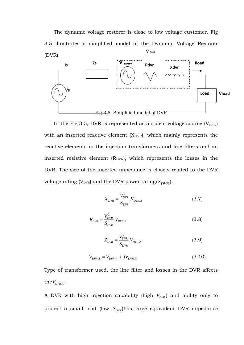
The dynamic voltage restorer is close to low voltage customer. Fig
3.5 illustrates a simplified model of the Dynamic Voltage Restorer
(DVR).
Fig 3.5: Simplified model of DVR
In the Fig 3.5, DVR is represented as an ideal voltage source (Vconv)
with an inserted reactive element (XDVR), which mainly represents the
reactive elements in the injection transformers and line filters and an
inserted resistive element (RDVR), which represents the losses in the
DVR. The size of the inserted impedance is closely related to the DVR
voltage rating (VDVR) and the DVR power rating ( )DVRS .
2
,.DVR
DVR DVR X
DVR
VX V
S (3.7)
2
,.DVR
DVR DVR R
DVR
VR V
S (3.8)
2
,.DVR
DVR DVR Z
DVR
VZ V
S (3.9)
, , ,DVR Z DVR R DVR XV V jV (3.10)
Type of transformer used, the line filter and losses in the DVR affects
the ,DVR ZV .
A DVR with high injection capability (high DVRV ) and ability only to
protect a small load (low DVRS )has large equivalent DVR impedance
Vs
Xdvr
Load Vload
Is Zs Rdvr Iload
V DVR
V conv

( DVRZ ). A high resistive part increases the energy, which should be
dissipated from the DVR and the costs associated with losses. High
total inserted DVR impedance increases the potential load voltage
fluctuations if the load is non-linear and /or has a fluctuating load
behavior. When DVR is connected to the medium voltage level, it
protects a large consumer or group of consumers. Inserting a large DVR
at the MV-level will only increase the supply impedance for a low
voltage load slightly. Some of the advantages of the high rated DVR at
the medium voltage level are:
If the distribution system is operated as a three wire system with
isolated or inductor grounded system, injection of positive and
negative sequence system is significant.
The costs per MVA to protect are expected to be lower if one large
central DVR is located at the medium voltage level instead of
decentralized low voltage units.
Some of the disadvantages of the high rated DVR at the medium voltage
level are:
Protecting a large load requires a medium voltage DVR otherwise the
losses in the DVR will be too high.
During ground faults in the medium voltage system the phase to
ground voltages can increase with 31/2, and a higher isolation level
may of the injection transformers must be ensured.
3.3.3 Operation of DVR
The DVR can be operated in three different modes which are
described as

1. Bypass mode: the Dynamic Voltage Restorer (DVR) is bypassed
mechanically or electronically during high load currents and down-
stream short circuits. In this mode the DVR cannot inject a voltage
to improve the voltage quality.
2. Standby mode: The supply voltages are at rated level and the DVR
is ready to compensate for voltage sag. During standby mode the
DVR can have secondary tasks and operation modes.
Loss less mode: The DVR performs no switching and the
losses in the DVR are minimized to conduction losses.
Harmonic blocking mode and voltage balancing mode:
The DVR improves the load voltage and compensate for
poor background voltage quality. The DVR has to perform
switching and is expected to inject a relatively small
voltage.
Capacitor emulation mode: The DVR is controlled to
operate as in inserted series capacitor, thereby it can
compensate for large line inductance and for inductance
inserter in conjunction with the DVR.
3. Active mode: Whenever voltage sags are detected, DVR injects the
missing voltage. In this mode DVR should ensure the unchanged
load voltage with minimum energy dissipation for injection due to
high cost of capacitors. The available voltage injection strategies are
pre-sag, phase advance, voltage tolerance and in phase method.
3.3.4 Voltage Injection Methods

Since the dynamic voltage restorer injects the compensating voltage
in order to maintain the load voltage constant, there are certain
limitations in compensating the voltage sags. The factors influencing
the compensation are finite power rating, different load conditions and
different types of voltage sag. Load characteristics dictate the control
strategy of dynamic voltage restorer as some loads are sensitive to
phase angle jump and others are tolerant to phase angle jump. The
injection compensating voltage is categorized as three methods.
1. Pre-sag Compensation: In this method DVR continuously
tracks the supply voltage. The DVR injects the missing voltage
between during sag and pre-sag voltages to the system. During
the compensation, DVR has to compensate both magnitude and
angle. The Fig 3.6 shows the vector representation of pre-sag
conditions. In this method, the injected power cannot be
controlled while load voltage can be restored ideally. Load
conditions and type of fault determines the injected power.
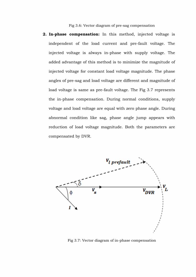
Fig 3.6: Vector diagram of pre-sag compensation
2. In-phase compensation: In this method, injected voltage is
independent of the load current and pre-fault voltage. The
injected voltage is always in-phase with supply voltage. The
added advantage of this method is to minimize the magnitude of
injected voltage for constant load voltage magnitude. The phase
angles of pre-sag and load voltage are different and magnitude of
load voltage is same as pre-fault voltage. The Fig 3.7 represents
the in-phase compensation. During normal conditions, supply
voltage and load voltage are equal with zero phase angle. During
abnormal condition like sag, phase angle jump appears with
reduction of load voltage magnitude. Both the parameters are
compensated by DVR.
Fig 3.7: Vector diagram of in-phase compensation

3. Phase-Advance Compensation: Active power is injected to
sensitive loads continuously in both pre-sag compensation and
In-phase compensation methods. In both methods, DVR
restoration time and performance are confined due to limited
energy storage capacity of dc link which limits the active power
injection. Phase advance methods proves to better compared to
other methods as it associates only reactive power injection
instead of active power. The injected active power is made zero
by injecting compensating voltage perpendicular to load current.
The injected voltage of the phase-advance method is larger than
those of pre-sag or in-phase method. The voltage phase shift in
phase advance method causes voltage waveform discontinuity,
inaccurate zero crossing and load power swing. Hence, phase-
advance compensation should be adjusted to the load that is
tolerant to phase angle jump or transition period should be
taken while the phase angle is moved from pre-fault angle to the
advance angle.

Fig 3.8: Vector diagram of phase advance compensation
3.3.5 DVR LIMITATIONS
Every circuit which has advantages will also have few
disadvantages. A DVR has limited capabilities and the DVR will most
likely to face voltage sag outside the range of full compensation. Some
of the limitations of DVR are:
Voltage limit: The design is limited in the injection capability to
keep the cost down and to reduce the voltage drop across the
device in standby operation
Current limit: The DVR has a limitation in current conduction
capability to keep the cost down.
Power limit: Power is stored in the DC link, but the bulk power
is often converted from supply itself or from a larger DC storage.
An additional converter is often used to maintain a constant DC-
link voltage and rating of the converter can introduce a power
limit to the DVR.

Energy limit: Energy is used to maintain the load voltage
constant and the storage is normally sized as low as possible in
order to reduce cost. Some sags will deplete the storage fast, and
adequate control can reduce the risk of load tripping caused be
insufficient energy storage.
Other limitations
The voltage injected can with an ideal DVR be done instantly, but
practical DVRs have a finite response-time and other factors may favor
a smooth change from one operating point to another. For the DVR a
slow change to stationary operating point will reduce the risk of in rush
currents and saturation of the transformer. From a load point of view a
fast change of the pre-sag voltage will make the voltage sag unseen. If a
phase change is initiated to minimize the energy storage depletion a
slow change to an adequate stationary operating point may prevent
severe transients and in worst case load tripping. All the limits should
be taken into consideration in the control strategy.
3.3.6 Modeling of DVR
With the Thevinin model of the DVR, the thevinin impedance is the
resultant of fixed resistance, which is equivalent to losses in the DVR
and fixed reactance, which is equivalent to reactive elements of the
DVR. Modeling of DVR includes the voltage handling capability, current
handling capability and size of energy storage. The voltage injection
capability of DVR can be expressed as
sup ,
% *100DVR
DVR
ply rated
VV
V (3.11)

The equipment cost and standby losses limit the voltage injection
capability of the DVR; should be chosen as low as possible. In addition
to voltage rating, current rating also affects the performance of DVR.
The parameters affecting current handling capability of the DVR are
inrush, non-linear loads, down stream short circuits, future increase of
load, standby losses and magnetization of injection transformer. Low
current rating results in overloading of VSC.
DVR L th L thV V Z I V (3.12)
The load current LI is given by
*
L LL
L
P jQI
V
(3.13)
The equation can be rewritten as
0 ( )DVR L th thV V Z V (3.14)
Where , and are the angles of DVR
V , thZ and thV respectively. is the
load power factor angle and is given by
1tan L
L
Q
P
(3.15)
Assuming the thevinin impedance is very less ( thZ << 1), the voltage
injected by the DVR can be written as
1DVR L th LV V V K V , (3.16)
Where K indicates the ratio of source voltage to the load voltage
th
L
VK
V (3.17)

Apparent power required by the DVR ( DVRS ) is then calculated in terms
of the apparent load power ( LS ).
(1 )DVR LS S K (3.18)
*
DVR DVR LS V I (3.19)
The active and reactive powers can be calculated by separating
apparent load power into its real and imaginary parts
sin( ) sin( )DVR L L sQ S K (3.20)
cos( ) cos( )DVR L L sP S K (3.21)
Where cos( )L and cos( )s are the load power factor and source power
factor.
cos1
cos
th L
DVR L
L
VP P
(3.22)
In the equation 3.22, the load voltage is assumed to be 1pu. The
required active power of a DVR depends on the magnitude and the
phase angle jump of supply voltage as well as the load power factor.
i. Converter Modeling
The main function of the Voltage Source Converter (VSC) is to convert
Dc signal into corresponding step ac signal. The thesis presents a
multilevel topology as VSC. The cascaded H bridge type with isolated
DC source is employed. The fig 3.9 represents the 5 level cascaded H
bridge leg for one phase. Cascaded H-bridge (CHB) multilevel inverter
employs multiple units of H-bridge power cells connected in series to
produce high ac voltage.

Fig 3.9: Configuration of five level H-bridge inverter for one phase
Fig 3.10: configuration of five level CHB inverter
The fig 3.10 represents the configuration of a five level CHB
inverter. If ‘m’ denotes the no. of voltage levels in a CHB inverter, the
no. of H-bridge cells (H) required in each phase is given by
1
2
mH
(3.23)
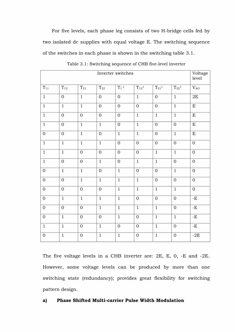
For five levels, each phase leg consists of two H-bridge cells fed by
two isolated dc supplies with equal voltage E. The switching sequence
of the switches in each phase is shown in the switching table 3.1.
Table 3.1: Switching sequence of CHB five-level inverter
Inverter switches Voltage level
T11 T12 T21 T22 T1`1 T12
1 T211 T22
1 VAO
1 0 1 0 0 1 0 1 2E
1 1 1 0 0 0 0 1 E
1 0 0 0 0 1 1 1 E
1 0 1 1 0 1 0 0 E
0 0 1 0 1 1 0 1 E
1 1 1 1 0 0 0 0 0
1 1 0 0 0 0 1 1 0
1 0 0 1 0 1 1 0 0
0 1 1 0 1 0 0 1 0
0 0 1 1 1 1 0 0 0
0 0 0 0 1 1 1 1 0
0 1 1 1 1 0 0 0 -E
0 0 0 1 1 1 1 0 -E
0 1 0 0 1 0 1 1 -E
1 1 0 1 0 0 1 0 -E
0 1 0 1 1 0 1 0 -2E
The five voltage levels in a CHB inverter are: 2E, E, 0, -E and -2E.
However, some voltage levels can be produced by more than one
switching state (redundancy); provides great flexibility for switching
pattern design.
a) Phase Shifted Multi-carrier Pulse Width Modulation

Phase Shifted Pulse Width Modulation (PSPWM) is one of the carrier
based modulation schemes or multilevel inverters. In the PSPWM, the
triangular carriers have the same frequency and same amplitude but
phase shifted by an angle. The no. of triangular carriers requires for five
levels inverter is given by
( 1)n m (3.24)
The phase shift between any two adjacent carrier waves is given by
360
( 1)cr
m
(3.25)
The frequency of the dominant harmonic in the inverter output voltage
determines the inverter switching frequency ,sw invf . For five levels CHB
inverter, the dominant harmonics in phase and line voltages are
distributed around4 fm . The term fm refers to frequency modulation
index (ratio of carrier signal frequency ( crf ) fundamental signal
frequency ( mf )). The inverter switching frequency is given by
, 4 *sw inv f mf m f (3.26)
The inverter requires small filter at the output. A large amount of
transient current flows through the inverter switches when inverters
are requested to generate a significant amount of voltages suddenly in a
step wise manner. This transient voltage can be reduced by over-sizing
of the inverter switches.
ii. AC Filter
Second order LC-type filters are widely used on the AC terminals of
PWM inverters when the output voltages are the main control targets.
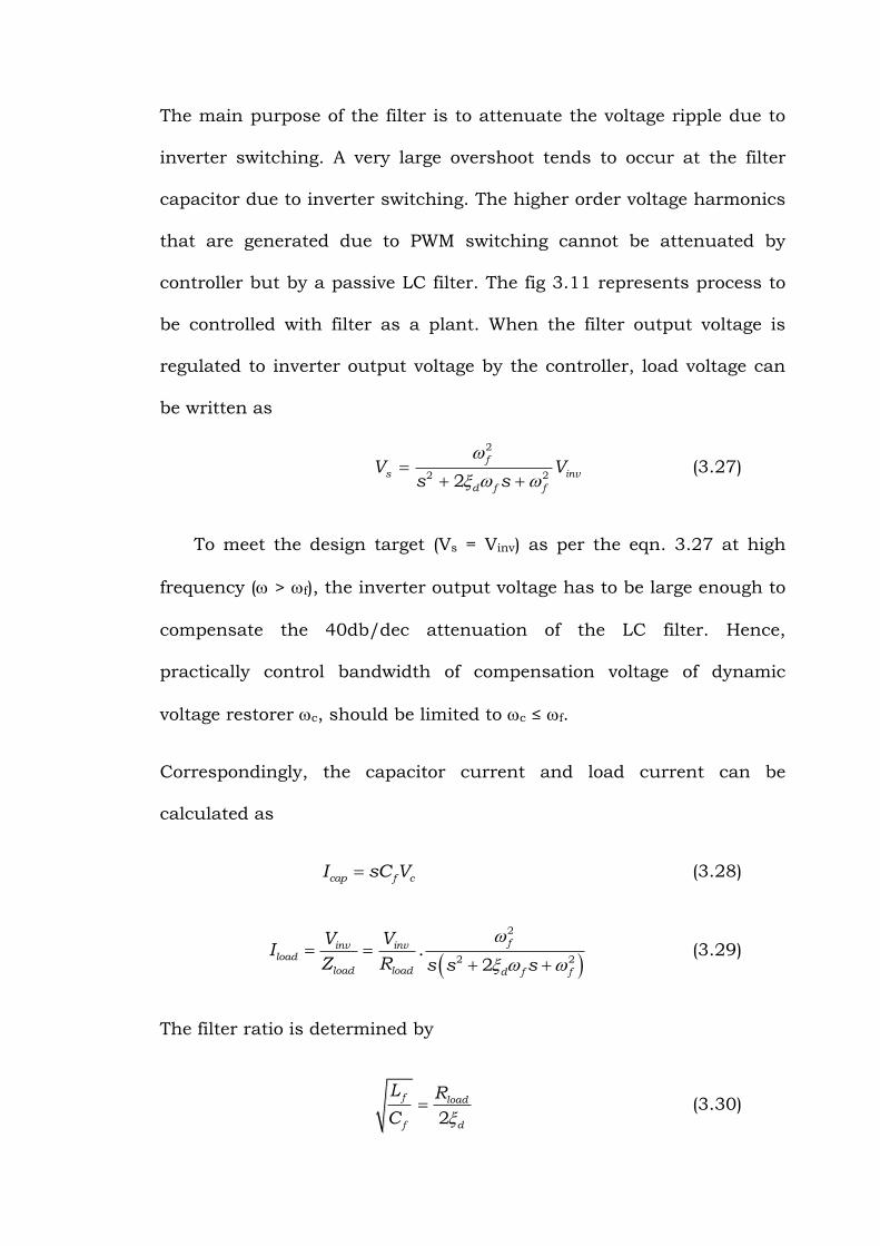
The main purpose of the filter is to attenuate the voltage ripple due to
inverter switching. A very large overshoot tends to occur at the filter
capacitor due to inverter switching. The higher order voltage harmonics
that are generated due to PWM switching cannot be attenuated by
controller but by a passive LC filter. The fig 3.11 represents process to
be controlled with filter as a plant. When the filter output voltage is
regulated to inverter output voltage by the controller, load voltage can
be written as
2
2 22
f
s inv
d f f
V Vs s
(3.27)
To meet the design target (Vs = Vinv) as per the eqn. 3.27 at high
frequency ( > f), the inverter output voltage has to be large enough to
compensate the 40db/dec attenuation of the LC filter. Hence,
practically control bandwidth of compensation voltage of dynamic
voltage restorer c, should be limited to c ≤ f.
Correspondingly, the capacitor current and load current can be
calculated as
cap f cI sC V (3.28)
2
2 2.
2
finv invload
load load d f f
V VI
Z R s s s
(3.29)
The filter ratio is determined by
2
f load
f d
L R
C (3.30)

In the case of pure resistive loads, the filter ratio may be taken as
f load
f d
L R
C to maintain the inverter output current under the rated
peak value in a transient state. For highly inductive loads, the filter
ratio can be set to
. df
load
f
LZ e
C
(3.31)
The main steps to be considered for filter design are:
Filter cut off frequency referring to the inverter switching
frequency
1
10sw
f
f fL C
(3.32)
Filter ratio referring to the rated load impedance and the control-
damping coefficient
f load
f d
L Z
C (3.33)
iii. DC energy storage
The DC energy storage supplies real power to the system during the
operation of DVR. A large DC capacitor needs to be connected in the
DVR to ensure constant input supply to inverter. The DC capacitor in
between the energy storage and inverter serves as the buffer to the
DVR, generating and absorbing power during voltage sag condition. The
size of the capacitor depends on the required active power to be injected

through DC storage capacity. However, the rating of the capacitor can
be calculated by
2
2( )active sag
dc
P TC
V (3.34)
sagT refers to duration of sag and activeP refers to the active power to be
injected by the DVR.
iv. Injection Transformer
The injection transformer function is to inject the missing voltage to
the line. Usually transformer either steps up or injects the voltage fed
from the out put of the filter before feeding to the line. The transformer
ratio can be defined as:
DVR
conv
Vn
V (3.35)
The ratio can be sized to have high utilization of the converter. The
short circuit impedance of a transformer which is the summation of
resistive and reactive elements has a major influence on the short
circuit current. The worst short circuit current can be calculated as
sup max
3
ply
sc
transformer
VI
Z (3.36)
3.4 PROCESS TO BE CONTROLLED
The fig 3.11 represents the part of the DVR referring to main
problem of the research work. In the fig when the DVR is operating, the
load current flows through the transformer secondary. A part of this

load current flow in the transformer primary in the opposite direction to
the filter current.
Fig 3.11: process to be controlled
The negative current reduces the magnitude of filter output voltage;
More DC voltage is required to inject the missing voltage. The negative
current also increases the stress on the inverter switches and PWM
controller. The output voltage of filter can be defined as
2 2
1
1 1s inv L
Ls RV V I
LCs RCs LCs RCs
(3.37)
The main function of dynamic voltage restorer is to regulate the
output compensation voltages according to the reference voltages and
to properly reject the disturbances from the load currents. The main
requirement for the voltage regulation and disturbance rejection is to:
1s
inv
V
V (3.38)
0L
s
I
V (3.39)

These equations refer to design targets to be achieved by suitable
control strategies.
3.5 OUTPUT SENSITIVITY FUNCTION
The fig 3.12 represents the closed loop block diagram for process to
be controlled. K and P refer to the plant and the controller. The transfer
function of the LC filter is considered as a plant.
Fig 3.12: Block diagram of process to be controlled
From the fig, the sensitivity functions can be derived to quantify the
system dynamics, robustness and noise rejection property of controller.
The three noises as shown in the fig 3.12 represents control noise uW ,
output noise yW and measurement noise bW . From the fig 3.12, the
sensitivity function can be written as
Output to output sensitivity function 1
1yyS
KP
Measure to output sensitivity function 1
yb
KPS
KP
Control to output sensitivity function 1
yy
PS
KP

The gradient of yyS at low frequency determines the dynamic
behavior of the system. The bandwidth of ybS defines the influence of
noise on the output voltage and the closed loop bandwidth. The gain of
yuS verifies the rejection of control perturbations such as PWM related
noises. In addition to the sensitivity functions, module margin can be
determined from the peak magnitude of yyS . The module margin M is
defined as minimum distance of yyL to the critical locus -1 in the
nyquist plot. The module margin and delay margin quantify the
robustness of the modeling uncertainties. The delay margin is given by
Where and represents the phase margin and frequency
corresponding to phase margin. For robust system, the module margin
must be less than 5db and delay margin must be higher than sampling
period.
Fig 3.13: Nyquist plot for yyL

3.6 CONTROL STRATEGIES
The control strategy is an algorithm to tune the controller
parameters so as to meet desired target. The research work is carried
for four different algorithms for tuning controller parameters. PI
controller, Internal Model Control, RST controller, artificial neural
control is the four different controllers used in the research to test the
performance of DVR.
3.6.1 PID Control
Generally PID controller performs three actions on the given
system. PID contains proportional, integral and derivative actions on
the system. The individual actions on the systems are as follows:
a) Proportional controller
Accelerates the process response with increase in gain.
Produces a steady state deviation in the absence of integrator in
the transfer function. This offset decreases with increase in
proportional gain.
b) Integral
Eliminates the steady state deviation
Response is sluggish with long oscillations
Increase of gain makes the system more oscillatory and leads to
instabilities
c) Derivative
Anticipates future errors
Introduces a stabilizing effect in the closed loop response.
To meet the design criteria, the plant is considered as LC filter.
2 7
2 2 2 2 7
1 1.66*10( )
1 2 333.33 1.66*10
n
n n
G s KLCs RCs s s s s
(3.40)
Where K is the system gain, L = 3mH, C = 2μF and R = 1Ω
ωn is the systems natural frequency= 4079rad/sec
is the systems damping ratio= 0.04.
The poles of the plant are -166.67+4079i.
Controller ( )p IK s K
C ss
(3.41)
Characteristic equation of this system is given by
3 2 2 2 22 ( )ch n n p n n IG s s K s K (3.42)
In order to design the controller gain values poles have to be located
based on the required transient parameters (Peak-overshoot, settling
time and Peak time).
Peak time 21
d
dM e
(3.43)
Settling time 4.6
s
d nd
T
(3.44)
Peak time 21
p
nd d
T
(3.45)
For the desired transient parameters, d and ωd can be obtained.
Since value in the plant is very less, d cannot be improved to 0.7.

Hence, it is selected based on the value of desired frequency. With the
obtained values, the closed loop characteristic equation with desired
damping ration and frequency can be written as
2 22chd d d dG s a s s (3.46)
Pole ‘a’ is selected so as to make the order of desired characteristic
equation and order of controller characteristic equation same. Usually
pole ‘a’ is a high frequency pole that allows the desired poles to
dominate the closed loop system response while allowing the desired
characteristic equation to have correct number of poles. The equation
can reduced to
3 2 2 2(2 ) ( 2 )chd d nd nd d nd ndG s a s a s a (3.47)
By comparing the eqns. 3.42 & 3.47, Kp and KI can be obtained
The simulink diagram for the step response of the closed loop system is
shown in the fig 3.14
Fig 3.14: Simulink diagram for step response of closed loop system

0 2 4 6 8 100
2
4
6
8
10
12
Time (secs)
Ampl
itud
e
Fig 3.15: Output response of PI controller without disturbance.
From the fig 3.15, it is evident that first desired condition is met
with the controller. The simulink diagram closed loop system with
disturbance is given by
Fig 3.16: Simulink diagram of closed loop system with disturbance
0 2 4 6 8 10-10
-5
0
5
10
15
20
Time (secs)
Am
plit
ude
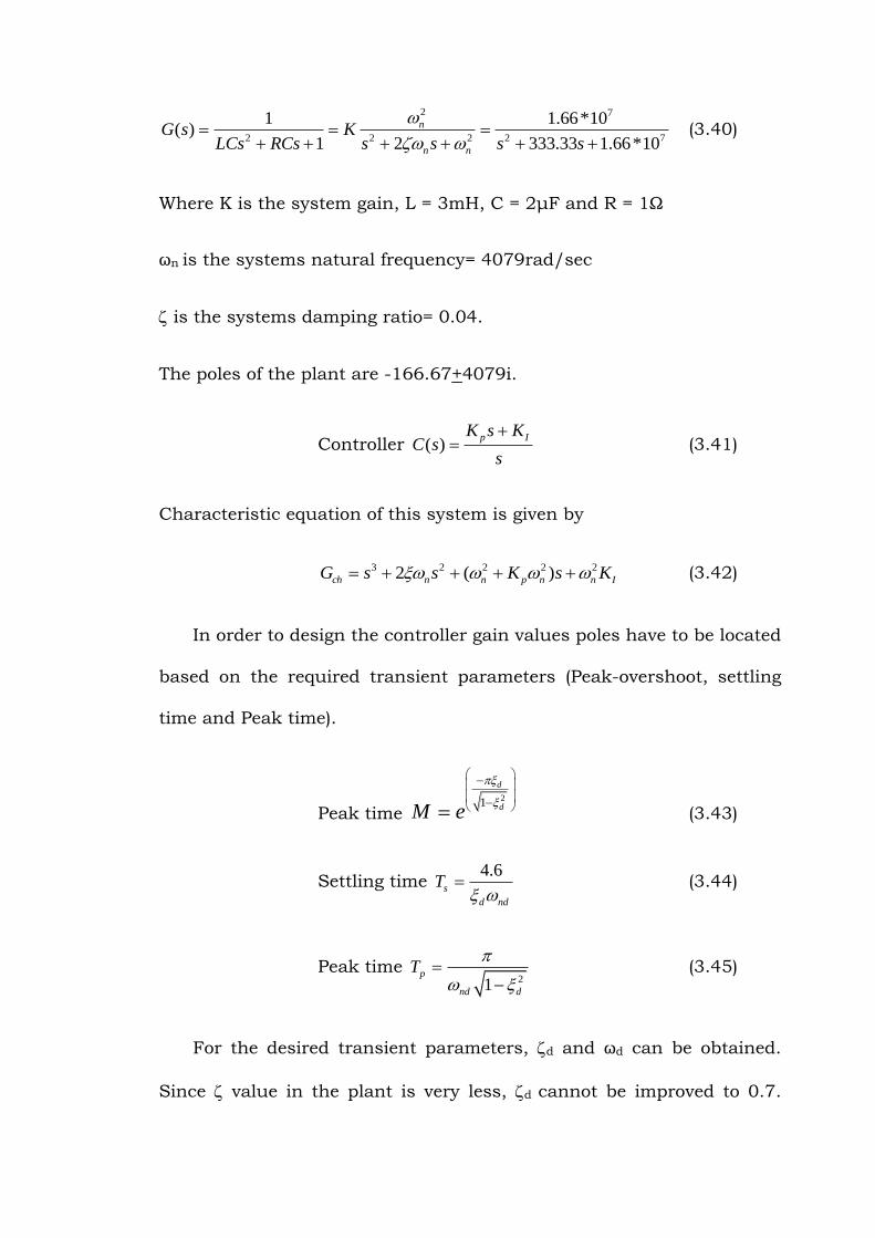
Fig 3.17: Step response with disturbance
It is very clear that with PID controller, the disturbance still exists
at the time of injection which is not desirable. Hence, PID controller
does not give good performance for DVR application.
The bode plot of the closed loop system is shown in fig 3.18. The
performance parameters for the robustness are:
Gain margin (GM): 5.74dB
Phase Margin (PM): 170deg and 2.29deg.

Bode Diagram
Frequency (rad/sec)
100
101
102
103
104
105
-225
-180
-135
-90
-45
0
Ph
ase (deg)
-80
-60
-40
-20
0
20
Magn
itu
de (dB
)
Fig 3.18: Closed loop bode plot with PI control
Bode Diagram
Frequency (rad/sec)
100
101
102
103
104
105
-45
0
45
90
135
180
Ph
ase
(deg)
-60
-40
-20
0
20
Magn
itu
de (dB
)
Fig 3.19: Output sensitivity plot
The output sensitivity function with PI control can be defined as

1
1oG
KP
(3.48)
K refers to PI controller transfer function and P refers to the plant
transfer function. The corresponding output sensitivity function is
shown in the fig 3.19. The peak gain of the output sensitivity function
should be less than 5db. In the fig, the peak gain is 19db, which is
clearly greater than the specified. This peak gain indicates that PI
controller does not have disturbance rejection capability.
3.7 SYSTEM DESCRIPTION
In the proposed work, System is composed of generating system,
transmission system and distribution system to show the complete
power system network. Generating system is a three phase source with
13KV, 50Hz. Generating system is fed to two transmission lines
through 3-winding transformers connected in star/delta/delta with a
voltage rating of 13/115/15KV. Such transmission lines feeds two
distribution networks through two transformers connected in
delta/star with voltage rating of 15/11KV. In the test system voltage
sag is created by creating a symmetrical three phase line fault in
distribution system with a fault resistance of 0.66Ω. This fault results
in 20% voltage sag at the utility end. Voltage interruption is created by
creating a three phase line fault with fault resistance of 0.001Ω. The
duration of voltage sag and interruption is 0.3s i.e. between 0.5secs to
0.8secs.
Different case studies are proposed in this thesis. First case study
includes performance analysis of dynamic voltage restorer feeding to RL

load mitigating voltage sag. Second case study includes performance
analysis of dynamic voltage restorer feeding to a rectifier load mitigating
voltage sag. Third case study includes performance analysis of dynamic
voltage restorer feeding to RL load mitigating voltage interruption.
Fourth case study includes performance analysis of dynamic voltage
restorer feeding to rectifier load mitigating voltage interruption.
Fig 3.20: Simulink diagram of the test system

0 0.2 0.4 0.6 0.8 1-1
0
1
Va(V
)
0 0.2 0.4 0.6 0.8 1-1
0
1
Vb(V
)
0 0.2 0.4 0.6 0.8 1-1
0
1
Time
Vc(V
)
Fig 3.21: Voltage sag with a fault resistance of 0.66Ω
0 0.2 0.4 0.6 0.8 10
0.1
0.2
0.3
0.4
0.5
0.6
0.7
0.8
0.9
1
Time
Magn
itu
de (pu
)
Fig 3.22: Load voltage magnitude in pu

0 0.2 0.4 0.6 0.8 1 1.2 1.4-1
0
1
Va(V
)
0 0.2 0.4 0.6 0.8 1 1.2 1.4-1
0
1
Vb(V
)
0 0.2 0.4 0.6 0.8 1 1.2 1.4-1
0
1
Time
Vc(V
)
Fig 3.23: Voltage interruption with fault resistance of 0.001ohms
0 0.1 0.2 0.3 0.4 0.5 0.6 0.7 0.8 0.9 10
0.1
0.2
0.3
0.4
0.5
0.6
0.7
0.8
0.9
1
Time
Magn
itu
de (pu
)
Fig 3.24: Load voltage magnitude in pu

3.8 SIMULATION RESULTS
Table 3.2: Test parameters
Parameters Values
Supply voltage 11kV
Filter Capacitance Cf 20µF
Filter inductance Lf 3mH
Filter resistance Rf 1
Proportional gain Kp 0.4142
Integral gain Ki 188.85
Load power factor 45deg lagging
Case 1: Voltage sag mitigation with PI control based DVR
Case 1 illustrates the operation of DVR for the mitigation of voltage
at the utility end with RL load. The PI controller is used for generating
reference signal for the PWM controller which in turn produces the
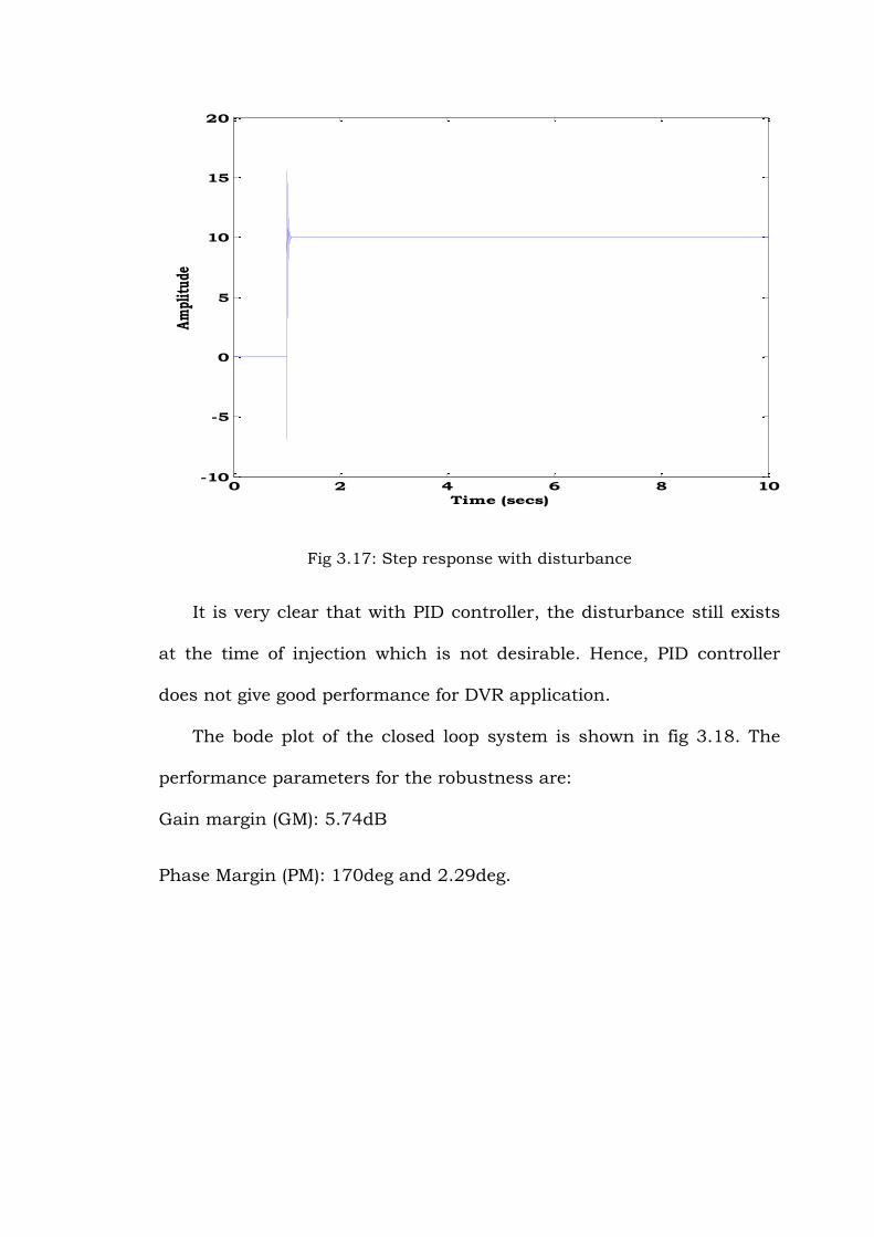
firing pulses for the multilevel inverter. The fig 3.25 depicts the load
voltage with DVR in operation between 0.5 to 0.8secs. As seen from the
figure, DVR is able to maintain load voltage at 98%. The injected
voltage from the DVR is free from harmonics. The response of a DVR for
the voltage sag is less than 4ms.
0.4 0.5 0.6 0.7 0.8 0.9 1-1
0
1
Va(V
)
0.4 0.5 0.6 0.7 0.8 0.9 1-1
0
1
Vb(V
)
0.4 0.5 0.6 0.7 0.8 0.9 1-1
0
1
Time
Vc(V
)
Fig 3.25: load voltage with PI control
0.4 0.5 0.6 0.7 0.8 0.9 1-1
0
1
Selected signal: 50.32 cycles. FFT window (in red): 25 cycles
Time (s)
0 2 4 6 8 100
5
10
15
20
Harmonic order
Fundamental (50Hz) = 0.9559 , THD= 1.20%
Mag (%
of
Fu
ndam
en
tal)
Fig 3.26: Total harmonic distortion with PI control
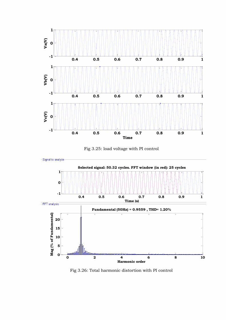
Case 2: DVR with rectifier load for mitigation of voltage sag
Case 2 illustrates the rectifier load connected to utility system. The
rectifier load is a non-linear load which distorts the load voltage and
current resulting in voltage and current harmonics. DVR operates
during the period of sag to maintain the load voltage at 98%. The DC
voltage required to mitigate the voltage is sag is . It is clearly seen from
the fig 3.27, that the DVR is injecting harmonic free voltage to the
utility end. The corressponding Total Harmonic Distortion (THD) is
shown in the fig 3.28. The time taken by the DVR to respond to voltage
sag is less than 4ms.
0.4 0.5 0.6 0.7 0.8 0.9 1-1
0
1
Va(V
)
0.4 0.5 0.6 0.7 0.8 0.9 1-1
0
1
Vb(V
)
0.4 0.5 0.6 0.7 0.8 0.9 1-1
0
1
Time
Vc(V
)
Fig 3.27: Load voltage with PI control with rectifier load

0.4 0.5 0.6 0.7 0.8 0.9 1-1
0
1
Selected signal: 50.46 cycles. FFT window (in red): 20 cycles
Time (s)
0 2 4 6 8 100
5
10
15
Harmonic order
Fundamental (50Hz) = 0.9793 , THD= 1.93%
Mag (%
of
Fu
ndam
en
tal)
Fig 3.28: Total harmonic distortion with PI control
Case 3: Mitigation of voltage interruption with PI control based
DVR
Case 3 depicts the creation and mitigation of voltage interruption at
the uitlity end. Usually in closed loop, DVR can inject only 50% of the
rated load voltage during voltage fluctuations. Here, open loop is used
to make the DVR to inject more than 50% of the rated load voltage.
Case 3 illustrates the capability of a DVR to mitigate voltage
interruption at the utility end with large DC energy stirage facility. The
basic idea is to study the effect of controller on the disturbance
rejection and DC storage capability. The fig 3.29 shows the load voltage
with DVR injecting voltage during the period of voltage interruption.
Since, the DVR has to inject a very large voltage (rated load voltage) a

small delay is observed at the starting of injection. This delay is due to
the time taken by the filter and PWM inverter to develop the voltage.
However, the load voltage is observed to be free from harmonics and
load voltage is maintained at 98% at the utility end. The corressponding
THD of the load voltage is observed to be 3.07% which is below the
value specified as per the standard.
0.4 0.5 0.6 0.7 0.8 0.9 1 1.1-1
0
1
Va(V
)
0.4 0.5 0.6 0.7 0.8 0.9 1 1.1-1
0
1
Vb(V
)
0.4 0.5 0.6 0.7 0.8 0.9 1 1.1-1
0
1
Time
Vc(V
)
Fig 3.29 Load voltage with Controller compensating interruption

0.4 0.5 0.6 0.7 0.8 0.9 1-1
0
1
Selected signal: 54.56 cycles. FFT window (in red): 25 cycles
Time (s)
0 1 2 3 4 5 6 7 8 9 100
20
40
60
Harmonic order
Fundamental (50Hz) = 0.7139 , THD= 3.07%
Mag (%
of
Fu
ndam
en
tal)
Fig 3.30: Total harmonic distortion with PI control
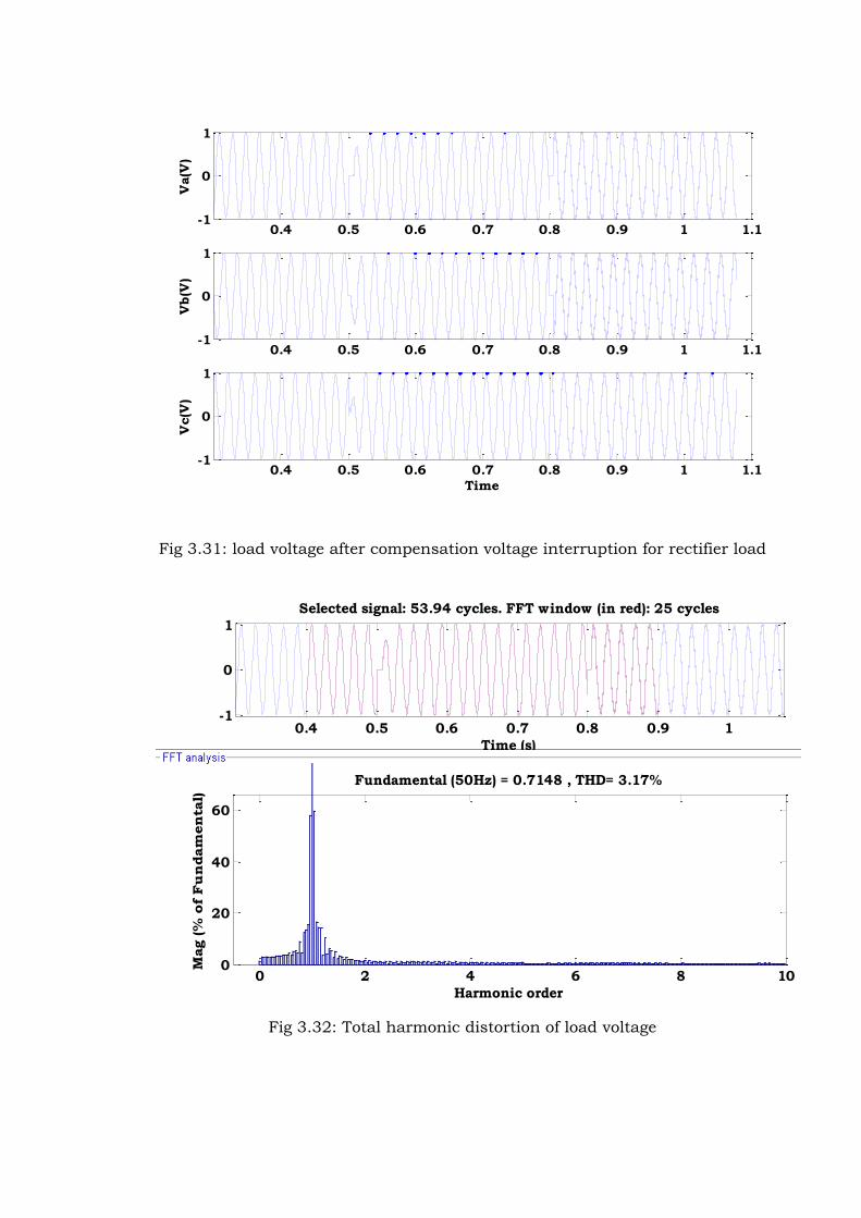
Case 4: DVR with rectifier load for mitigation of voltage
interruption
Case 4 describes the utility system connected to rectifier load. The
non linearity nature of the rectifier load distorts the load voltage and
current. This case study depicts the controller capability to reduce the
harmonics and disturbance rejection with non linear load. The DVR is
employed with isolated DC energy storage with open loop control. Since
the DVR has to inject complete rated load voltage it takes some time to
respond which is clearly observed in the fig 3.31 as small delay.
However, the DVR is able to maintain the load voltage at 98%. The
corresponding THD of the load voltage is observed to be 3.17% which is
lesser than the standard.
0.4 0.5 0.6 0.7 0.8 0.9 1 1.1-1
0
1
Va(V
)
0.4 0.5 0.6 0.7 0.8 0.9 1 1.1-1
0
1
Vb(V
)
0.4 0.5 0.6 0.7 0.8 0.9 1 1.1-1
0
1
Time
Vc(V
)
Fig 3.31: load voltage after compensation voltage interruption for rectifier load
0.4 0.5 0.6 0.7 0.8 0.9 1-1
0
1
Selected signal: 53.94 cycles. FFT window (in red): 25 cycles
Time (s)
0 2 4 6 8 100
20
40
60
Harmonic order
Fundamental (50Hz) = 0.7148 , THD= 3.17%
Mag (%
of
Fu
ndam
en
tal)
Fig 3.32: Total harmonic distortion of load voltage

3.9 SUMMARY
In this chapter power quality issues for a DVR have been treated
and the focus has been on voltage sags, interruptions and the power
electronic controllers for voltage sag mitigation.
Voltage sags can in many cases be the most severe power quality
problem because they can occur very frequently and lead to a
load tripping. The depth of voltage sag, duration and phase jump
depend on the location of the fault and the protection equipment
used.
Voltage sag can be caused by faults at all voltage levels. The
voltage sag size and symmetry depend mainly on the type of fault,
grounding principles used at the faulted voltage level and the
transformer connections between the fault and the load of
interest.
The mitigation of voltage sags can be achieved with power
electronic controllers. The series controller is recognized as a cost
effective solution for voltage sag mitigation.
The series controller has its limitations in which it can provide
the best performance.
Voltage injection methods for a series controller illustrate the
voltage disturbance handling capability under certain limitations.
The multilevel topology for series controller is effective in
reducing the DC energy storage thereby reducing the cost. The
cascade H-Bridge topology with isolated DC source can be
advantageous compared to other topologies.

The modeling of various parts of the series controller is
described.
The objective of the research work i.e process to be controlled
needs a good controller inorder to satisfy the desired targets. PI
controller is tuned with pole placement method. The PI controller
response to step disturbance is very poor indicating its weakness
in disturbance rejection.
The test system includes transmission and two distribution
systems. The voltage sag and interruptions are created by
creating faults with 0.66 and 0.001Ω. Some case studies are
illustrated with RL load and rectifier load mitigating voltage sag
and interruption.
With pole placement technique, PI controller can provide good
voltage regulation, but cannot reject the disturbance. Hence DC
storage energy required to inject missing voltage is high.