chapter 1 physics of bulk solids - john wiley &...
TRANSCRIPT
&CHAPTER 1
Physics of Bulk Solids
In this text we will be discussing the physics and chemistry of nanostructures. Thematerials used to form these structures generally have bulk properties that becomemodified when their sizes are reduced to the nanorange; the present chapter presentsbackground material on bulk properties of this type. Much of what is discussed herecan be found in a standard text on solid-state physics.1–4
1.1. STRUCTURE
1.1.1. Size Dependence of Properties
Many properties of solids depend on the size range over which they are measured.Microscopic details become averaged when investigating bulk materials. At themacro- or large-scale range ordinarily studied in traditional fields of physics suchas mechanics, electricity and magnetism, and optics, the sizes of the objects understudy range from millimeters to kilometers. The properties that we associate withthese materials are averaged properties, such as the density and elastic moduli inmechanics, the resistivity and magnetization in electricity and magnetism, and thedielectric constant in optics. When measurements are made in the micrometer or nano-meter range many properties of materials change, such as mechanical, ferroelectric,and ferromagnetic properties. The aim of the present book is to examine character-istics of solids at the next lower level of size, namely, the nanoscale level, perhapsfrom 1 to 100 nm. Below this there is the atomic scale near 0.1 nm, followed bythe nuclear scale near a femtometer (10215 m). In order to understand properties atthe nanoscale it is necessary to know something about the corresponding propertiesat the macroscopic and mesoscopic scales, and the present chapter aims to providesome of this background.
Many important nanostructures are composed of the group IV elements Si or Ge,types III–V semiconducting compounds such as GaAs or types II–VI semiconduct-ing materials such as CdS, so these semiconductor materials will be used to illustratesome of the bulk properties that become modified when their dimensions are reduced
The Physics and Chemistry of Nanosolids. By Frank J. Owens and Charles P. Poole, Jr.Copyright # 2008 John Wiley & Sons, Inc.
1
COPYRIG
HTED M
ATERIAL

to the nanometer range. These Roman numerals IV, III, V, and, so on refer to columnsof the periodic table. Tabulations of various bulk properties of these semiconductorsare found in Appendix B.
1.1.2. Crystal Structures
Most solids are crystalline with their atoms arranged on sites of a regular lattice struc-ture. They possess “long-range order” because this regularity extends throughout theentire crystal. In contrast to this amorphous materials such as glass and wax lack long-range order, but they have “short-range order,” which means that the local environ-ment of each atom is similar to that of other equivalent atoms, but this regularitydoes not persist over appreciable distances. In other words, each atom of a particulartype might have, for example, six nearest neighbors, and these neighboring atomsmight be at positions that approximate an octahedral configuration. Liquids alsohave short-range order, but lack long-range order, and this short-range order is under-going continual rearrangements as a result of Brownian motion. Gases lack both long-range and short-range order. Their constituent molecules undergo rapid translationalmotion in all directions, so the disorder is continually rearranging at a rapid rate.
Figure 1.1 shows the five regular arrangements of lattice points that can occur in twodimensions, namely, the square (a), primitive rectangular (b), centered rectangular (c),hexagonal (d), and oblique (e) kinds. These arrangements are called Bravais lattices.The general or oblique Bravais lattice has two unequal lattice constants a = b and anarbitrary angle u between them. For the perpendicular case when u ¼ 908, the latticebecomes rectangular, and if in addition a ¼ b, the lattice is called square. For thespecial case a ¼ b and u ¼ 608, the lattice is hexagonal, formed from equilateraltriangles. Each lattice has a unit cell, indicated in the figures, which can replicatethroughout the plane and generate the lattice.
A crystal structure is formed by associating with a lattice a regular arrangement ofatoms or molecules. Figure 1.2 presents a two-dimensional crystal structure based ona primitive rectangular lattice containing two diatomic molecules A–B in each unitcell. A single unit cell can generate the overall lattice.
In three dimensions there are three lattice constants, a, b, and c, and three angles: abetween b and c, b between a and c, and g between lattice constants a and b. Thereare 14 Bravais lattices, ranging from the lowest symmetry triclinic type in whichall three lattice constants and all three angles differ from each other (a = b = c
Figure 1.1. The five Bravais lattices that occur in two dimensions, with the unit cells indi-cated: (a) square; (b) primitive rectangular; (c) centered rectangular; (d) hexagonal; (e) oblique.
2 PHYSICS OF BULK SOLIDS

and a = b= g), to the highest-symmetry cubic case in which all the lattice constantsare equal and all the angles are 908 (a ¼ b ¼ c and a ¼ b¼ g ¼ 908). There are threeBravais lattices in the cubic system: a primitive or simple cubic (sc) lattice in whichthe atoms occupy the eight apices of the cubic unit cell, as shown in Fig. 1.3a; a body-centered cubic (bcc) lattice with lattice points occupied at the apices and in the centerof the unit cell, as indicated in Fig. 1.3b; and a face-centered cubic (fcc) Bravaislattice with atoms at the apices and in the centers of the faces, as shown in Fig. 1.3c.
In two dimensions the most efficient way to pack identical circles (or spheres) isthe equilateral triangle arrangement shown in Fig. 1.4a, corresponding to the hexago-nal Bravais lattice of Fig. 1.1d. A second hexagonal layer of spheres can be positionedon top of the first to form the most efficient packing of two layers, illustrated inFig. 1.4b. For efficient packing, the third layer can be placed either above the firstlayer with an atom at the location indicated by T or in the third possible arrangementwith an atom above the position marked by X on the figure. In the first case a hexa-gonal lattice structure called hexagonal close-packed (hcp) is generated, and in thesecond case a fcc lattice results. The former is easy to identify in a unit cell, butthe latter is not so easy to visualize while looking at a unit cell since the close-packed planes are oriented perpendicular to the [111] direction.
In three dimensions the unit cell of the fcc structure is the cube shown in Fig. 1.3c,which has a side (i.e., lattice constant) a and volume a3. It has six face-centeredatoms, each shared by two unit cells, and eight apical atoms, each shared by eightunit cells, corresponding to a total of four for this individual unit cell. Nearest
Figure 1.2. Sketch of a two-dimensional crystal structure based on a primitive rectangularlattice containing two diatomic molecules A–B in each unit cell.
Figure 1.3. Unit cells of the three cubic Bravais lattices: (a) simple cubic (sc); (b) body-centered cubic (bcc); (c) and face-centered cubic (fcc).
1.1. STRUCTURE 3

neighbors are a distance a/(2)1/2 apart, so the atomic radius is defined as one-half ofthis value, namely, rA ¼ a/2(2)1/2. Since there are four atoms per unit cell the volumedensity is rV ¼ 4/a3. Each spherical atom has the individual volume 4p rA
3 /3, so thepacking fraction or percentage of the unit cell volume occupied by the atoms isp/3(2)1/2 ¼ 0.7406. Figure 1.5 illustrates an alternate way to present the unit cellof the fcc lattice. There are one atom in the center, and there are 12 atoms at theedges. Each edge atom is shared by four unit cells so it counts as one-fourth ofthis particular cell, and the centrally located atom is not shared, corresponding tothe expected total of four for this particular unit cell.
If only the 13 atoms shown in Fig. 1.5 are present, then the configuration constitutesthe nanoparticle displayed in Fig. 1.6; this is discussed in the next section. This nano-particle may be assumed to consist of three layers of two-dimensional close-packedplanes perpendicular to its body diagonal or [111] axis, as indicated in Fig. 1.7.
Figure 1.4. Close packing of spheres on a flat surface (a) for a monolayer and (b) with a secondlayer added. The circles of the second layer are drawn smaller for clarity. The location of an octa-hedral site is indicated by X, and the position of a tetrahedral site is designated by T in (b).
Figure 1.5. Face-centered cubic unit cell showing the 12 nearest-neighbor atoms that surroundthe atom (darkened circle) in the center.
4 PHYSICS OF BULK SOLIDS

Figure 1.6. A 13-atom nanoparticle set in its fcc unit cell, showing the shape of the 14-sidedpolyhedron associated with the nanoparticle. The three open circles at the upper right corre-spond to the top layer, the six solid circles plus the atom (not pictured) in the center of thecube constitute the middle hexagonal layer, and the open circle at the lower left corner ofthe cube is one of the three atoms at the bottom layer of the cluster.
Figure 1.7. A 13-atom nanocluster set in its fcc centered cubic unit cell, delineating the planarconfigurations of the 13 included atoms. The 7-atom (darkened circles) plane in the center liesbetween the 3-atom (unshaded circles) plane at the upper right and the 3-atom partly hiddenplane at the rear. Figure 1.6 provides a similar perspective.
1.1. STRUCTURE 5

There is a centrally located seven-atom close-packed plane (blackened circles),sandwiched between a pair of three-atom close-packed planes (unshaded circles).Two of the three atoms of the lower such plane are obscured from view on thefigure. The distance between adjacent planes is one-third of the length (3)1/2 a ofthe body diagonal, or a/(3)1/2. The apex of the cube along this body diagonal isthe distance a=2(3)1=2 above the upper close-packed (three-atom) plane, and it is theposition of an octahedral site equidistant between two close-packed planes. Theatom configurations presented in Fig. 1.7 provide an easy way to visualize the relation-ships between fcc close-packed planes.
In the three-dimensional arrangements of close-packed spheres there are spaces orsites between the spheres where smaller atoms can reside. These sites exist betweenpairs of close-packed layers, so they are independent of the manner in which a thirdlayer is added. In other words, they are the same for fcc and hcp lattices.
The point marked by X on Fig. 1.4b is called an octahedral site since it isequidistant from the three spheres O below it, and from the three spheres O aboveit, and these six nearest neighbors constitute the apices of an imaginary octahedron.An atom A at this site has the local coordination AO6. The radius aoct of this octa-hedral site is
aoct ¼14
(2� (2)1=2)a ¼ ((2)1=2 � 1)a0 ¼ 0:41411a0 (1:1)
where a is the lattice constant and a0 is the sphere radius. The number of octahedralsites is equal to the number of spheres. There are also smaller sites called tetrahedralsites, labeled T on the figure that are equally distant from four nearest-neighborspheres, one below and three above, corresponding to AO4 for the local coordination.These four spheres define an imaginary tetrahedron surrounding an atom A located atthe site. This is a smaller site since its radius aT is
aT ¼14
((3)1=2 � (2)1=2)a ¼ [(3=2)1=2 � 1]a0 ¼ 0:2247a0 (1:2)
There are twice as many tetrahedral sites as spheres in the structure. Many diatomicoxides and sulfides such as MgO, MgS, MnO, and MnS possess larger oxygenor sulfur anions in a perfect fcc arrangement with the smaller metal cationslocated at octahedral sites. This is an NaCl lattice, where we use the term anionfor a negative ion (e.g., Cl2), and cation for a positive ion (e.g., Naþ). Themineral spinel MgAl2O4 has a face-centered arrangement of divalent oxygensO22 (radius 0.132 nm) with the Al3þ ions (radius 0.051 nm) occupying one-halfof the octahedral sites and Mg2þ (radius 0.066 nm) located in one-eighth of thetetrahedral sites in a regular manner. In some spinels the oxygens deviate somewhatfrom a perfect fcc arrangement by moving slightly toward or away from the tetra-hedral sites.
6 PHYSICS OF BULK SOLIDS

1.1.3. Face-Centered Cubic Nanoparticles
Most metals in the solid-state form close-packed lattices; thus Ag, Al, Au, Co, Cu, Pb,Pt, and Rh, as well as the rare gases Ne, Ar, Kr, and Xe, are fcc, and Mg, Nd, Os, Re,Ru, Y, and Zn are hcp. Some other metallic atoms crystallize in the more looselypacked bcc lattice, and a few such as Cr, Li, and Sr crystallize in all three structuretypes, depending on the temperature. An atom in each of the two close-packed latticeshas 12 nearest neighbors. Figure 1.5 shows the 12 neighbors that surround an atom(darkened circle) located in the center of a cube for a fcc lattice. In Fig. 1.7 weshow a redrawn version of the fcc unit cell of Fig. 1.6 that clarifies the layered struc-ture of the atoms. The topmost layer is an equilateral triangle of atoms (open circles);the next layer below is a regular hexagon of atoms (blackened circles); and the bottomlayer, another equilateral triangle of open circle atoms, is mostly hidden from view.These 13 atoms constitute the smallest theoretical nanoparticle for an fcc lattice.More precisely it should probably be called a nanocluster. Figure 1.6 shows the14-sided polyhedron, called a dekatessarahedron, that is generated by connectingthe nearest-neighbor atoms. This polyhedron has six square faces and eight equilateraltriangle faces. Figure 1.8 shows this polyhedron viewed from the [111] or top direc-tion with the coordinate axis perpendicular to each side indicted. The square sides areperpendicular to the x axis [100], the y axis [010], and the z axis [001], respectively,and the triangular faces are perpendicular to the indicated body diagonal directions.Figure 1.7 clarifies the layering scheme by connecting atoms only within two-dimensional close-packed layers. The three open circles in the triangular layer ofFig. 1.7 are the three atoms in the top layer of Fig. 1.8. Likewise, the seven darkened
Figure 1.8. Perspective along the [111] direction of the faces or facets of the 13-atom fccnanoparticle of Fig. 1.6. The three visible square faces are perpendicular to the x direction[100], the y direction [010], and the z direction [001], respectively. The four equilateral trianglefaces are perpendicular to body diagonal directions, as indicated.
1.1. STRUCTURE 7
circles, including the atom in the center of the cube of Fig. 1.7, constitute the periph-ery of Fig. 1.8.
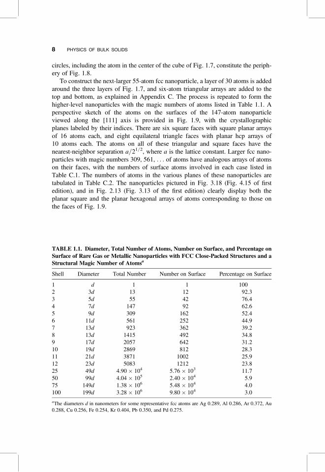
To construct the next-larger 55-atom fcc nanoparticle, a layer of 30 atoms is addedaround the three layers of Fig. 1.7, and six-atom triangular arrays are added to thetop and bottom, as explained in Appendix C. The process is repeated to form thehigher-level nanoparticles with the magic numbers of atoms listed in Table 1.1. Aperspective sketch of the atoms on the surfaces of the 147-atom nanoparticleviewed along the [111] axis is provided in Fig. 1.9, with the crystallographicplanes labeled by their indices. There are six square faces with square planar arraysof 16 atoms each, and eight equilateral triangle faces with planar hcp arrays of10 atoms each. The atoms on all of these triangular and square faces have thenearest-neighbor separation a/21/2, where a is the lattice constant. Larger fcc nano-particles with magic numbers 309, 561, . . . of atoms have analogous arrays of atomson their faces, with the numbers of surface atoms involved in each case listed inTable C.1. The numbers of atoms in the various planes of these nanoparticles aretabulated in Table C.2. The nanoparticles pictured in Fig. 3.18 (Fig. 4.15 of firstedition), and in Fig. 2.13 (Fig. 3.13 of the first edition) clearly display both theplanar square and the planar hexagonal arrays of atoms corresponding to those onthe faces of Fig. 1.9.
TABLE 1.1. Diameter, Total Number of Atoms, Number on Surface, and Percentage onSurface of Rare Gas or Metallic Nanoparticles with FCC Close-Packed Structures and aStructural Magic Number of Atomsa
Shell Diameter Total Number Number on Surface Percentage on Surface
1 d 1 1 1002 3d 13 12 92.33 5d 55 42 76.44 7d 147 92 62.65 9d 309 162 52.46 11d 561 252 44.97 13d 923 362 39.28 13d 1415 492 34.89 17d 2057 642 31.210 19d 2869 812 28.311 21d 3871 1002 25.912 23d 5083 1212 23.825 49d 4.90 � 104 5.76 � 103 11.750 99d 4.04 � 105 2.40 � 104 5.975 149d 1.38 � 106 5.48 � 104 4.0100 199d 3.28 � 106 9.80 � 104 3.0
aThe diameters d in nanometers for some representative fcc atoms are Ag 0.289, Al 0.286, Ar 0.372, Au0.288, Cu 0.256, Fe 0.254, Kr 0.404, Pb 0.350, and Pd 0.275.
8 PHYSICS OF BULK SOLIDS

1.1.4. Large Face-Centered Cubic Nanoparticles
Larger fcc nanoparticles with the same polyhedral shape are obtained by adding moreplanes or layers, and the sequence of numbers in the resulting particles, N ¼1,13,55,147,309, . . . , listed in Table 1.1, are called structural magic numbers. Forn layers the number of atoms N in this fcc nanoparticle is given by the formula
N ¼ (1=3)[10n3 � 15n2 þ 11n� 3] (1:3)
and the number of atoms on the surface Nsurf is
Nsurf ¼ 10n2 � 20nþ 12 (1:4)
Equation (1.3) is valid for all n, but Eq. (1.4) is valid only for n . 1. For each value ofn Table 1.1 lists the number of atoms on the surface, as well as the percentage ofatoms on the surface. The table also lists the diameter of the each nanoparticle,which is given by the expression (2n 2 1)d, where d is the distance between thecenters of nearest-neighbor atoms and d ¼ a/(2),1/2, where a is the lattice constant.
Purely metallic fcc nanoparticles such as Au55 tend to be very reactive and haveshort lifetimes. They can be ligand-stabilized by adding atomic groups betweentheir atoms and on their surfaces. The Au55 nanoparticle has been studied in theligand-stabilized form Au55(PPh3)12Cl6, which has the diameter of �1.4 nm,where PPh3 is an organic group. Further examples are the magic number nanoparti-cles Pt309(1,10-phenantroline)36O30, and Pd561(1,10-phenantroline)36O200.
The magic numbers that we have been discussing are called structural magicnumbers because they arise from minimum-volume, maximum-density nanoparticles
Figure 1.9. Arrays of atoms on triangular and square faces of the 147-atom fcc nanoparticle.The directions perpendicular to each face are indicated.
1.1. STRUCTURE 9

that approximate a spherical shape, and have close-packed structures characteristic ofa bulk solid. These magic numbers take no account of the electronic structure of theconstituent atoms in the nanoparticle. Sometimes the predominant factor in determin-ing the minimum-energy structure of small nanoparticles is the interactions betweenthe valence electrons of the constituent atoms with an averaged molecular potential,so that the electrons occupy orbital levels associated with this potential. Atomiccluster configurations in which these electrons fill closed shells are especiallystable, and constitute electronic magic numbers. Their atomic structures differ fromthe fcc arrangement, as will be discussed in Section 3.2.
When mass spectra were recorded for sodium nanoparticles NaN it was found thatmass peaks corresponding to the first 15 electronic magic numbers N ¼ 3,9,20,36,61,. . . were observed for cluster sizes up to N ¼ 1220 atoms (n ¼ 15), and fcc structuralmagic numbers starting with N ¼ 1415 for n ¼ 8 were observed for larger sizes.5,6
The mass spectral data are plotted versus the cube root of the number of atomsN1/3 on Fig. 1.10, and it is clear that the lines from both sets of magic numbersare approximately equally spaced, with the spacing between the structural magicnumbers about 2.6 times that between the electronic ones. This result is evidencethat small clusters tend to satisfy electronic criteria, and large structures tend to bestructurally determined.
1.1.5. Tetrahedrally Bonded Semiconductor Structures
Types III–V and II–VI binary semiconducting compounds, such as GaAs and ZnS,respectively, crystallize with one atom situated on a fcc sublattice at positions 000,12
12 0, 1
2 0 12, and 0 1
212, and the other atom on a second fcc sublattice displaced from
the first by the amount 14
14
14 along the body diagonal, as shown in Fig. 1.11b. This is
called the zinc blende or ZnS structure. It is clear from the figure that each Zn atom(white sphere) is centered in a tetrahedron of S atoms (black spheres), and likewiseeach S has four similarly situated Zn nearest neighbors. The small half-sized,dashed-line cube delineates one such tetrahedron. The same structure would result ifthe Zn and S atoms were interchanged. Figure 1.12 presents a more realistic sketchof the unit cell of ZnS with the small zinc atoms centered in the tetrahedral sites of
Figure 1.10. Dependence of the observed mass spectra lines from NaN nanoparticles on thecube root N1/3 of the number of atoms N in the cluster. The lines are labeled with the indexn of their respective electronic and structural magic numbers. [Adapted from T. P. Martin,T. Bergmann, H. Gohlich, and T. Lange, Chem. Phys. Lett. 172, 209 (1990).]
10 PHYSICS OF BULK SOLIDS

the larger sulfur atoms. In contrast to this arrangement, the atoms in the semiconductorgallium arsenide have comparable radii rGa ¼ 0.122 nm and rAs ¼ 0.124 nm, and thelattice constant a ¼ 0.565 nm is close to the value 4(rGa þ rAs)/(3)1/2 ¼ 0.568 nm, asexpected, where data were used from Tables B.1 and B.2 (of Appendix B).
Figure 1.11. Unit cell of the diamond structure (a) containing only one type of atom, and cor-responding unit cell of the zinc blende structure (b) containing two atom types. The rods rep-resent the tetrahedral bonds between nearest-neighbor atoms. The small dashed-line cube in (b)delineates a tetrahedron. (From G. Burns, Solid State Physics, Academic Press, Boston, 1985,p. 148.)
Figure 1.12. Packing of larger sulfur atoms and smaller zinc atoms in the zinc blende (ZnS)structure. Each atom is centered in a tetrahedron of the other atom type. (From R. W. G.Wyckoff, Crystal Structures, Vol. 1, Wiley, New York, 1963, p. 109.)
1.1. STRUCTURE 11
The elements Si and Ge crystallize in this same structure, in which the Si (or Ge)atoms occupy all the sites on the two sublattices, so there are eight identical atoms inthe unit cell. This atom arrangement, sketched in Fig. 1.11a, is called the “diamondstructure.” Both Si and Ge have a valence of 4, so from bonding considerations it isappropriate for each to be bound to four other atoms in the shape of a regular tetrahedron.
In Table B.1 we see the lattice constants a listed for various compounds with thezinc blende structure, and Table B.2 provides the crystal radii of their monatomic lat-tices in which the atoms are uncharged, as well as the ionic radii for ionic compoundsin which the atoms are charged. We see from Table B.2 that the negative anions areconsiderably larger than the positive cations, in accordance with the sketch of the unitcell presented in Fig. 1.12, and this size differential is greater for the III–V com-pounds than for II–VI compounds. However, these size changes for the negativeand positive ions tend to balance each other so that the III–V compounds have thesame range of lattice constants as do the II–VI compounds, with Si and Ge also inthis range. Table B.4 gives the molecular masses, and Table B.5 gives the densitiesof these semiconductors. The three tables, Tables B.1, B.4, and B.5, show a regularprogression in the values as one goes from left to right in a particular row, and as onegoes from top to bottom in a particular column. This occurs because of the systematicincrease in the size of the atoms in each group with increasing atomic number, asindicted in Table B.2.
There are two simple models for representing these AC binary compound struc-tures. For an ionic model the lattice An2Cnþ consists of a fcc arrangement of thelarge anions An2 with the small cations Cnþ located in the tetrahedral sitesof the anion fcc lattice. If the anions touch each other, their radii has the value r ¼a/2(2)1/2, where a is the lattice parameter, and the radius aT of the tetrahedral sitertetr ¼ 0.2247 a is given by Eq. (1.2). This is the case for the very small Al3þ
cation in the AlSb structure. In all other cases the cations in Table B.2 are toolarge to fit in the tetrahedral site, so they push the larger anions further apart, andthe latter no longer touch each other, in accordance with Fig. 1.12. In a covalentmodel for the structure consisting of neutral atoms A and C the atom sizes are com-parable, as the data in Table B.2 indicate, and the structure resembles that of Si or Ge.Comparing these two models, we note that the distance between atom A at lattice pos-ition 000 and its nearest neighbor C at position 1
414
14 is equal to 1
4 (3)1=2a, and inTable B.3 we compare this crystallographically evaluated distance with the sums ofradii of ions An2, Cnþ from the ionic model, and with the sums of radii of neutralatoms A and C of the covalent model using the data of Table B.2. We see fromthe results in Table B.3 that neither model fits the data in all cases, but the neutralatom covalent model is closer to agreement, especially for ZnS, GaAs, and CdS.For comparison purposes we also list corresponding data for several alkali halidesNaCl, KBr, and RbI, and alkaline-earth chalcogenides CaS and SrSe, which alsocrystallize in the cubic rock salt or NaCl structure. We see that all of these compoundsfit the ionic model very well. In these compounds each atom type forms a fcc lattice,with the atoms of one fcc lattice located at octahedral sites of the other lattice. Theoctahedral site has the radius roct ¼ 0.41411 a0 given by Eq. (1.1), which is largerthan the tetrahedral one, rtetr ¼ 0.2247 a, of Eq. (1.2).
12 PHYSICS OF BULK SOLIDS

Since the alkali halide and alkaline-earth chalcogenide compounds fit the ionicmodel so well, it is significant that neither model fits the structures of the semicon-ductor compounds. The extent to which the semiconductor crystals exhibit ionic orcovalent bonding is not clear from crystallographic data. If the wavefunction describ-ing the bonding is written in the form
C ¼ acovccov þ aioncion (1:5)
where the coefficients of the covalent and ionic wavefunction components arenormalized
acov2 þ aion
2 ¼ 1 (1:6)
then acov2 is the fractional covalency and aion
2 is the fractional ionicity of the bond. Achapter in a recent book by Karl Boer7 tabulates the effective charges e� associatedwith various II–VI and III–V semiconducting compounds, and this effective chargeis related to the fractional covalency by the expression
acov2 ¼ 8� N þ e�
8(1:7)
where N ¼ 2 for II–VI and N ¼ 3 for III–V compounds. The fractional charges alllie in the range from 0.43 to 0.49 for the compounds under consideration. Using thee� tabulations in the Boer book and Eq. (1.7), we obtain the fractional covalencies ofacov
2 � 0:81 for all the II–VI compounds, and acov2 � 0:68 for all the III–V com-
pounds listed in Tables B.1, B.4, B.5, and so on. These values are consistent withthe better fit of the covalent model to the crystallographic data for these compounds.
We conclude this section with some observations that will be of use in later chap-ters. Table B.1 shows that the typical compound GaAs has the lattice constant a ¼0.565 nm, so the volume of its unit cell is 0.180 nm3, corresponding to about 22 ofeach atom type per cubic nanometer. The distances between atomic layers in the[100], [110], and [111] directions are, respectively, a/2 ¼ 0.28 nm, a/(2)1/2 ¼
0.40 nm, and a/(3)1/2 ¼ 0.33 nm, for GaAs. The various III–V semiconductingcompounds under discussion form mixed crystals over broad concentration ranges,as do the group of II–VI compounds. In a mixed crystal of the type InxGa12xAs,it is ordinarily safe to assume that Vegard’s law is valid, whereby the lattice constanta scales linearly with the concentration parameter x. As a result, we have the follow-ing relationships
a(x) ¼ a(GaAs)þ [a(InAs) � a(GaAs)]x
¼ 0:565þ 0:039x (1:8)
where 0 , x , 1. In the corresponding expression for the mixed semiconductorAlxGa12xAs the term �0.003x replaces the term þ0.039x, so the fraction of lattice
1.1. STRUCTURE 13

mismatch 2jaAlAs 2 aGaAsj/(aAlAs þ aGaAs) ¼ 0.0054 ¼ 0.54% for this system isquite minimal compared to that 2jaInAs 2 aGaAsj/(aInAs þ aGaAs) ¼ 0.066 ¼ 6.6%of the InxGa12xAs system, as calculated from Eq. (1.8). Table B.1 of Appendix Bgives the lattice constants a for various III–V and II–VI semiconductors with thezinc blende structure.
1.1.6. Lattice Vibrations
We have discussed atoms in a crystal as residing at particular lattice sites, but inreality they undergo continuous fluctuations in the neighborhood of their regular pos-itions in the lattice. These fluctuations arise from the heat or thermal energy in thelattice, and become more pronounced at higher temperatures. Since the atoms arebound together by chemical bonds, the movement of one atom about its sitecauses the neighboring atoms to respond to this motion. The chemical bonds actlike springs that stretch and compress repeatedly during the oscillatory motion. Theresult is that many atoms vibrate in unison, and this collective motion spreadsthroughout the crystal. Every type of lattice has its own characteristic modes or fre-quencies of vibration called normal modes, and the overall collective vibrationalmotion of the lattice is a combination or superposition of many, many normalmodes. For a diatomic lattice like GaAs, there are low-frequency modes called acous-tic modes, in which the heavy and light atoms tend to vibrate in phase or in unisonwith each other, and high-frequency modes called optical modes, in which theytend to vibrate out of phase.
A simple model for analyzing these vibratory modes is a linear chain of alternatingatoms with a large mass M and a small mass m joined to each other by springs (�) asfollows:
� m � M � m � M � m � M � m � M �
When one of the springs stretches or compresses by an amount Dx, a force isexerted on the adjacent masses with the magnitude C Dx, where C is the spring con-stant. As the various springs stretch and compress in step with each other, longitudi-nal modes of vibration take place in which the motion of each atom is along the stringdirection. Each such normal mode has a particular frequency v and a wavevector k ¼2p/l, where l is the wavelength, and the energy E associated with the mode is givenby E ¼h�v. There are also transverse normal modes in which the atoms vibrate backand forth in directions perpendicular to the line of atoms. Figure 1.13 shows thedependence of v on k for the low-frequency acoustic and the high-frequencyoptical longitudinal modes. We see that the acoustic branch continually increasesin frequency v with increasing wavenumber k, and the optical branch continuouslydecreases in frequency. The two branches have respective limiting frequenciesgiven by (2C/M )1/2 and (2C/m)1/2, with an energy gap between them at the edgeof the Brillouin zone kmax ¼ p/a, where a is the distance between atoms m and M
14 PHYSICS OF BULK SOLIDS

at equilibrium. The Brillouin zone is a unit cell in wavenumber or reciprocal space, aswill be explained in Section 1.3.2 later in this chapter. The optical branch vibrationalfrequencies are in the infrared region of the spectrum, generally with frequencies inthe range from 1012 to 3 � 1014 Hz, and the acoustic branch frequencies are muchlower. In three dimensions the situation is more complicated, and there are longitudi-nal acoustic (LA), transverse acoustic (TA), longitudinal optical (LO), and transverseoptical (TO) modes.
The atoms in molecules also undergo vibratory motion, and a molecule containingN atoms has 3N 2 6 normal modes of vibration. Particular molecular groups such ashydroxyl 22OH, amino 22NH2, and nitro 22NO2 have characteristic normal modesthat can be used to detect their presence in molecules and solids.
The atomic vibrations that we have been discussing correspond to standing waves.This vibrational motion can also produce traveling waves in which localized regionsof vibratory atomic motion travel through the lattice. Examples of such travelingwaves are sound moving through the air, or seismic waves that start at the epicenterof an earthquake and travel thousands of miles to reach a seismograph detector thatrecords the earthquake event many minutes later. Localized traveling waves of atomicvibrations in solids, called phonons, are quantized with the energy h�v ¼ hn, wheren ¼ v/2p is the frequency of vibration of the wave. Phonons play an importantrole in the physics of the solid state.
Figure 1.13. Dependence of the longitudinal normal-mode vibrational frequency v on thewavenumber k ¼ 2p/l for a linear diatomic chain of atoms with alternating masses m , Mhaving an equilibrium spacing a, and connected by bonds with spring constant C. [FromC. P. Poole, Jr., The Physics Handbook, Wiley, New York, 1998, p. 53.)
1.1. STRUCTURE 15

1.2. SURFACES OF CRYSTALS
1.2.1. Surface Characteristics
When we consider the bulk properties of macroscopic crystals, the surface layers playa negligible role. If a simple cubic crystal in the shape of a cube contains 1024 atoms,then each face of the cube will contain 1016 atoms, for a total of 6 � 1016 on thesurface. This is less than one atom in 107 on the surface, so the bulk is not appreciablyaffected by the presence of the surface. On the other hand, when we consider particlesin the nanoscale range of dimensions, the percentage of the atoms on the surface canbe large. We see from Table 1.1 that an aluminum nanoparticle with a diameter49d ¼ 14.0 nm contains 4.9 � 104 atoms, 11.7% of which are on the surface. Thelargest aluminum nanoparticle listed in the table has a diameter of 56.9 nm and con-tains 3.28 million atoms, 3% of which are on the surface. As a result, the surface caninfluence the bulk properties. The same is true of thin films with nanometer thick-nesses. For example, consider a fcc thin film consisting of 100 close-packed layers(the [111] axis is perpendicular to the surface). Such a film made of copper wouldbe 21 nm thick. Since there is both a top surface and a bottom surface, it followsthat 2% of the atoms are in a surface layer.
We have been discussing surface layers as if they are identical to the layers in thebulk, and this is seldom the case. Within the crystal the bonding orbitals of all theatoms are satisfied, and each type of atom is in the same environment as its counter-parts. In contrast to this, the surface atoms have dangling bonds that are not satisfied,and this deficiency of chemical bonding can be characterized quantitatively by asurface energy per unit area. This surface energy results from the work that mustbe done to cleave the crystal and break the dangling surface bonds while formingthe surface. Sometimes a surface atom reconstruction takes place to lower thissurface energy. For example, the [111] surface of a silicon (or germanium) crystalconsists of a hexagonal array of Si atoms, each of which, shown unshaded, has asingle vertical dangling bond indicated by a dot in Fig. 1.14. Each surface atom onthe figure is bonded to three Si atoms shown shaded in the layer below the surface.The energy is lowered by the surface reconstruction illustrated in Fig. 1.15, inwhich surface atoms move together and bond to each other in pairs to accommodateand satisfy the broken dangling bonds. Another phenomenon that sometimes takesplace is surface structure relaxation in which the outer layer of atoms moves slightlytoward or a short distance away from the layer below. Contraction takes place withmost metal surfaces. The silicon [111] surface layer illustrated in Figs. 1.14 and1.15 contracts by about 25%, and the three interlayer spacings further below compen-sate for this by expanding between 1% and 5%.
Other phenomena can occur at the surface. Sometimes there are steps on thesurface beyond which a new layer has been added. Various types of defects canoccur, such as added atoms in an irregular manner, or missing atoms at latticesites. Surface atoms can bond together in ways that differ from those in the bulk,as took place in the reconstruction pictured in Fig. 1.15. Occasionally surfaceatoms will undergo a two-dimensional phase transition.
16 PHYSICS OF BULK SOLIDS

1.2.2. Surface Energy
Work must be done to cut a crystal into two pieces that expose a pair of new crystalfaces or facets. The energy required to bring about this cleavage, called the surfaceenergy, is proportional to the density of the various types of chemical bonds thatare cut and transformed into dangling bonds. In the case of fcc crystals, each largeatom has 12 large atom nearest neighbors to which it can be bonded. Eachmedium-sized atom in an octahedral site is bonded to six surrounding large atoms,and each small atom in a tetrahedral site is bonded to four large atoms. Whichbonds break depends on the particular crystallographic plane where the cleavageoccurs.
If the surface contains a density ri of atoms of type i, each with ni dangling bondsof energy 21i, then the surface energy density g or energy per unit area is given by thefollowing sum over the atom types
g ¼ Srini1i (1:9)
where the factor of 2 takes into account the fact that the energy associated with a dan-gling bond is half of the corresponding chemical bond energy. If all of the atoms are
Figure 1.14. Sketch of the first two [111] outermost layers of the zinc blende structureshowing unshaded sulfur atoms on the surface with vertical dangling bonds denoted bydots, and shaded zinc atoms one layer below the surface.
1.2. SURFACES OF CRYSTALS 17

identical as in the fcc and hcp lattices discussed above, this expression reduces to
g ¼ rn1 (1:10)
In the next few sections we will evaluate this surface energy density for severalspecial cases.
1.2.3. Face-Centered Cubic Surface Layers
We have been discussing how surface layers become modified relative to bulk layersin a crystal. Since many nanoparticles and nanofilms have a fcc structure, it will beinstructive to consider the arrangement of the atoms on the surfaces of fcc cubicsolids that are cleaved along particular crystallographic planes. Consider a solidwith large atoms close-packed so that they touch all 12 nearest neighbors, and withthe octahedral sites filled with medium-sized atoms in contact with their 6 nearestneighbors, and the tetrahedral sites occupied by small atoms in contact with their 4
Figure 1.15. Sketch of the surface configuration of Fig. 1.14 after it has undergone a recon-structuring process during which surface sulfur atoms bond together in pairs.
18 PHYSICS OF BULK SOLIDS

nearest neighbors. The radii of these three types of atoms have the following valuesfrom Eqs. (1.1) and (1.2)
rL ¼ 0:7072a (1:11a)
rOh ¼ 0:4142a (1:11b)
rT ¼ 0:2247a (1:11c)
where a is the lattice constant. Figure 1.16 shows an example of the octahedral sitesoccupied by smaller atoms, as happens in the NaCl structure. The zinc blende struc-ture of Fig. 1.11 has half of the tetrahedral sites and none of the octahedral sites occu-pied. It is clear from these figures that some of the octahedral sites lie on the surface ofthe unit cell, while all of the tetrahedral ones are inside it. If the crystal is cleaved toexpose the [100] face, it is evident from Fig. 1.16 that the surface will contain 50%larger and 50% smaller atoms, the latter occupying the octahedral sites of the former,as shown in Fig. 1.17 (i.e., 4 small half-atoms þ 1 large atom þ 4 large quarter-atoms). The [110] face displayed in Fig. 1.18 contains all three types of atoms.This can be seen by comparison with Figs. 1.11b and 1.16. The upper two tetra-hedrally coordinated atoms on Fig. 1.18 are shaded to indicate that they are absentin the zinc blende structure. The [111] plane displayed in Fig. 1.4a contains onlythe main large atoms since none of the tetrahedral or octahedral sites are in thisplane, as can be deduced from the positions of these sites specified in Fig. 1.4b.
Figure 1.16. Unit cell consisting of fcc atoms (large circles) with the octahedral holesoccupied by smaller atoms (small circles).
1.2. SURFACES OF CRYSTALS 19

There are several special cases that can be clarified from the analysis above. If allof the atoms are of the same size and only octahedral sites are occupied, then thelattice reduces to a simple cubic one with the lattice constant a/2, and a unit cellone-eighth of the size. Since nanoparticles are rarely simple cubic, we will notdiscuss this case further. An important special case is when none of these extrasites are occupied so only the large atoms are present. This is the situation that
Figure 1.17. The [100] surface plane of the structure depicted in Fig. 1.16.
Figure 1.18. The [110] surface plane of a fcc structure formed by large atoms with the octa-hedral sites occupied by medium-sized atoms and the tetrahedral sites occupied by small atoms.The upper two small atoms shown shaded as well as the three medium-sized atoms are absent inthe zinc blende structure.
20 PHYSICS OF BULK SOLIDS

corresponds to the fcc nanoparticles discussed in Section 1.1.3. The [100] face shownin Fig. 1.17 with the surface unit cell area a2 contains two atoms, one entire atom inthe center and four-quarters of an atom in the corners, so the atom density on thesurface is 2/a2 (the smaller atoms in the figure are now absent). The center atomhas four nearest neighbors inside the crystal face below it, four neighbors alongsideit in the face, and four missing nearest neighbors above so four of its chemicalbonds have been cut, and are now dangling bonds. This means that the number ofdangling bonds per unit area is 8/a2, and the surface energy density fromEq. (1.10) is g ¼ 81/a2. By similar reasoning, the [110] face unit cell shown inFig. 1.18 with the surface unit cell area (2)1/2a2 contains two atoms, so the atomdensity on the surface is (2)1/2/a2. Each surface atom is bonded to five atomsbelow it and to two surface atoms, so it has five dangling bonds, for a danglingbond density of 5(2)1/2/a2, and a surface energy density g of 5(2)1/21/a2. The[111] surface sketched in Fig. 1.19 is a little more complex to analyze.The rhombic unit cell outlined in the figure contains one atom and has the area(3)1/2a2/4. Each atom is bonded to three atoms below and six in the surface, so thereare three dangling bonds, for a dangling bond density of 4(3)1/2/a2, and a surfaceenergy density g of 4(3)1/21/a2. These results are gathered together in Table 1.2.
1.2.4. Surfaces of Zinc Blende and Diamond Structures
The remaining structure that is of interest is the diamond structure depicted inFig. 1.11. This consists of a set of fcc atoms together with a second set occupyinghalf of the tetrahedral holes of the first set, as was discussed above. We willdiscuss surfaces of ZnS crystals in which the small zinc atoms reside in the tetrahedral
Figure 1.19. Surface unit cell of the close-packed lattice sketched in Fig. 1.4a.
1.2. SURFACES OF CRYSTALS 21

sites of the dominant fcc sulfur lattice. The atom locations in various faces can bededuced from Figs. 1.11b and 1.12.
Figure 1.17, with the smaller octahedral site atoms omitted, depicts the [001]surface, which corresponds to the top face of the cubic unit cell in Figs. 1.11b and1.12. The atom density of this face is 2/a2, the same as in the simple fcc case dis-cussed above. It is clear from Fig. 1.11b that each surface atom has two danglingbonds, so the dangling bond density is 4/a2. Figure 1.18 sketches the [110]surface, which contains four large edge and apex S atoms of the surface unit cell,plus two smaller interior Zn atoms depicted by small open circles in the lower partof Fig. 1.18. In this figure the medium-sized octahedral site atoms and the shadedsmall tetrahedral site atoms are absent, so there are four atoms per surface unit cellof area (2)1/2a2. It is clear from Fig. 1.11b that each atom has two bonds withinthe surface and one below it, so there is one dangling bond per atom, for a danglingbond density of 2(2)1/2/a2. For simplicity we presume a surface energy density2(2)1/2a2, assuming that the dangling bond energy 1i of the zinc and sulfur atomshas the same value 1, which is really not the case. Figure 1.14 depicts the atomsassociated with the [111] plane. The unshaded circles represent the atoms on thesurface, and the shaded circles correspond to the first layer below the surface.Either type could be sulfur, and the other one would be zinc. The atom density is4/(3)1/2a2 as in the fcc cubic case discussed above. The dots centered in the opencircles denote dangling bonds, one such bond per atom, directed upward perpendicu-lar to the surface. Hence the dangling bond density is 4/(3)1/2a2.
We showed above how the energy of the atoms close to the [111] face of adiamond or zinc blende crystal can decrease by a reconstruction in which theatoms rearrange to a lattice with a bimolecular unit cell formed from the pairs ofatoms depicted in Fig. 1.15. These surface atoms bond in pairs so that there are nodangling bonds remain and the energy is lowered. In some cases the spacingbetween layers slightly varies between the surface and the bulk, with the layersnear the surface undergoing an expansion outward or a contraction inward. InFig. 1.14 the atoms with upward-directed bonds formed the surface. If the layerbelow had formed the surface, then each surface atom would have had three danglingbonds, a higher-energy situation, which is therefore unlikely to occur. Surfaces tendto form which minimize the density of dangling bonds.
TABLE 1.2. Atom Density, Number of Bonds Broken per Atom, and Surface EnergyDensity for Various Facets or Surfaces of FCC centered cubic and diamond structuresa
Structure and Facet Atom Density Bonds per Atom Surface-energy Density
Fcc [100] 2/a2 4 81/a2
Fcc [110] (2)1/2/a2 5 5(2)1/2 1/a2
Fcc [111] 4/a2 3 4(3)1/2 1/a2
Diamond [100] 2/a2 2 41/a2
Diamond [110] 2(2)1/2/a2 1 2(2)1/2 1/a2
Diamond [111] 4/a2 1 41/(3)1/2a2
aKey: a¼ lattice constant; 1 ¼ surface energy per dangling chemical bond.
22 PHYSICS OF BULK SOLIDS

Sometimes silicon forms a crystal with the external shape of an octahedron whichhas eight [111] faces that minimize the surface energy. On other occasions the octa-hedron is truncated in the manner illustrated in Fig. 1.20 since a truncated configur-ation has a lower surface energy for the same volume of crystal.
A favorable technique for studying surface structure is low-energy electron diffrac-tion (LEED). Another technique is reflection high-energy electron diffraction(RHEED) carried out at grazing incidence. These techniques are discussed inChapter 2.
1.2.5. Adsorption of Gases
Since surfaces generally have dangling bonds, they can be chemically very reactive.Owing to this reactivity, they readily adsorb gases in contact with them. Adsorbedmolecules are held in place on the surface by a binding energy DHads called theheat of adsorption. When chemical bonding takes place between surface atomsand adsorbed atoms or molecules, the phenomenon is called chemisorption. Thisbonding can be of either a covalent or an ionic type. If a much weaker van derWaals type of bonding occurs the phenomenon is referred to as physisorption. It iscustomary to call the process physisorption when the heat of adsorption is lessthan �10 kcal/mol, and to label it chemisorption when the heat of adsorptionexceeds 10 kcal/mol. For example, H2 and O2 molecules chemisorb on molybdenumwith DHads values of 40 kcal/mol and 172 kcal/mol, respectively.
The surface of a solid can be considered as the outermost layer of atoms plus theregion between 0.5 and 1.5 nm above and below it. This includes the bonding elec-trons on the inside and the dangling bonds on the outside. We are talking about an
Figure 1.20. Truncated octahedron. For a fcc crystal the atoms on the square faces have asquare lattice configuration, and the atoms on the hexagon shaped faces have a hexagonalclose packed coniiguration. (From G. Burns, Solid State Physics, Academic Press, Orlando,FL, 1985, p. 676.)
1.2. SURFACES OF CRYSTALS 23

atomically clean surface, one exposed to an ultrahigh vacuum, and which contains noadsorbed atoms or molecules. An ultrahigh vacuum is one in which the pressure isless than 1028 Pa (,7.5 � 10211 torr). When a molecule from the surroundinggas strikes the surface, there is a probability S called the sticking coefficient that itwill stick to the surface, that is, that it will be adsorbed. In a standard vacuum of1026 torr it will take surrounding gas molecules with a sticking coefficient S ¼ 1about one second to build up a monolayer, whereas at 10210 torr the monolayerbuildup time is much longer than an hour.
Figure 1.21. (a) Calculated potential energy and charge density as a function of z for metallicsodium. The Naþ ion cores of the last two atomic layers are indicated by brackets. [From J. A.Applebaum and D. R. Hamann, Phys. Rev. B6, 2166 (1972)]. (b) Calculated electron densitynear the surface of metallic Na, where rs ¼ 2 A is close to the Na value rs ¼ 2.08 A. [FromN. D. Lang and W. Kohn, Phys. Rev. B1, 4555 (1970). See also G. Burns (cited inFig. 1.20 legend), p. 703.]
24 PHYSICS OF BULK SOLIDS
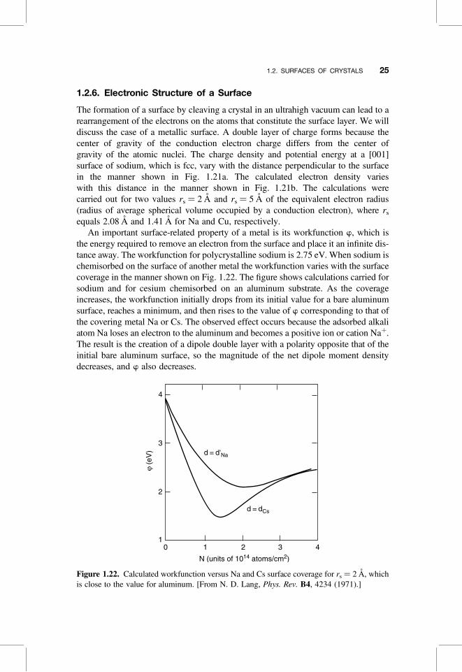
1.2.6. Electronic Structure of a Surface
The formation of a surface by cleaving a crystal in an ultrahigh vacuum can lead to arearrangement of the electrons on the atoms that constitute the surface layer. We willdiscuss the case of a metallic surface. A double layer of charge forms because thecenter of gravity of the conduction electron charge differs from the center ofgravity of the atomic nuclei. The charge density and potential energy at a [001]surface of sodium, which is fcc, vary with the distance perpendicular to the surfacein the manner shown in Fig. 1.21a. The calculated electron density varieswith this distance in the manner shown in Fig. 1.21b. The calculations werecarried out for two values rs ¼ 2 A and rs ¼ 5 A of the equivalent electron radius(radius of average spherical volume occupied by a conduction electron), where rs
equals 2.08 A and 1.41 A for Na and Cu, respectively.An important surface-related property of a metal is its workfunction w, which is
the energy required to remove an electron from the surface and place it an infinite dis-tance away. The workfunction for polycrystalline sodium is 2.75 eV. When sodium ischemisorbed on the surface of another metal the workfunction varies with the surfacecoverage in the manner shown on Fig. 1.22. The figure shows calculations carried forsodium and for cesium chemisorbed on an aluminum substrate. As the coverageincreases, the workfunction initially drops from its initial value for a bare aluminumsurface, reaches a minimum, and then rises to the value of w corresponding to that ofthe covering metal Na or Cs. The observed effect occurs because the adsorbed alkaliatom Na loses an electron to the aluminum and becomes a positive ion or cation Naþ.The result is the creation of a dipole double layer with a polarity opposite that of theinitial bare aluminum surface, so the magnitude of the net dipole moment densitydecreases, and w also decreases.
Figure 1.22. Calculated workfunction versus Na and Cs surface coverage for rs ¼ 2 A, whichis close to the value for aluminum. [From N. D. Lang, Phys. Rev. B4, 4234 (1971).]
1.2. SURFACES OF CRYSTALS 25
1.2.7. Surface Quantum Well
A quantum well is a three-dimensional structure in which two dimensions are large,perhaps a centimeter or a millimeter, and the third is in the nanometer range. Thesurface of a solid, with or without the presence of a layer of adsorbed gas molecules,may be regarded as a quantum well. It has a regular structure, its lateral dimensionsare macroscopic, and its thickness is several nanometers. It has characteristic chargeand potential energy distributions, as discussed above. Quantum wells are discussedin Chapter 9.
1.3. ENERGY BANDS
1.3.1. Insulators, Semiconductors, and Conductors
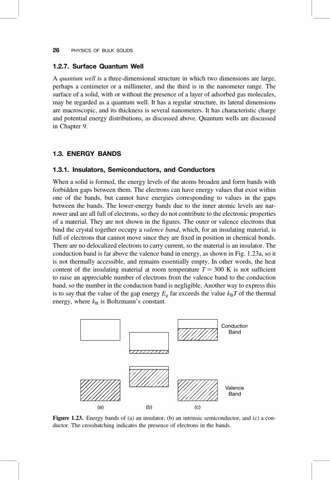
When a solid is formed, the energy levels of the atoms broaden and form bands withforbidden gaps between them. The electrons can have energy values that exist withinone of the bands, but cannot have energies corresponding to values in the gapsbetween the bands. The lower-energy bands due to the inner atomic levels are nar-rower and are all full of electrons, so they do not contribute to the electronic propertiesof a material. They are not shown in the figures. The outer or valence electrons thatbind the crystal together occupy a valence band, which, for an insulating material, isfull of electrons that cannot move since they are fixed in position in chemical bonds.There are no delocalized electrons to carry current, so the material is an insulator. Theconduction band is far above the valence band in energy, as shown in Fig. 1.23a, so itis not thermally accessible, and remains essentially empty. In other words, the heatcontent of the insulating material at room temperature T ¼ 300 K is not sufficientto raise an appreciable number of electrons from the valence band to the conductionband, so the number in the conduction band is negligible. Another way to express thisis to say that the value of the gap energy Eg far exceeds the value kBT of the thermalenergy, where kB is Boltzmann’s constant.
Figure 1.23. Energy bands of (a) an insulator, (b) an intrinsic semiconductor, and (c) a con-ductor. The crosshatching indicates the presence of electrons in the bands.
26 PHYSICS OF BULK SOLIDS

For a semiconductor, the gap between the valence and conduction bands is muchless, as shown in Fig. 1.23b, so Eg is closer to the thermal energy kBT, and the heatcontent of the material at room temperature can bring about the thermal excitation ofsome electrons from the valence band to the conduction band where they carrycurrent. The density of electrons reaching the conduction band by this thermal exci-tation process is relatively low, but by no means negligible, so the electrical conduc-tivity is small; hence the name semiconducting. A material of this type is called anintrinsic semiconductor. A semiconductor can be doped with donor atoms thatdonate electrons to the conduction band where they can carry current. The materialcan also be doped with acceptor atoms that obtain electrons from the valence bandand leave behind positive charges called holes which can also carry current. Theenergy levels of these donors and acceptors lie in the energy gap, as shown inFig. 1.24. The former produces N type, that is, negative charge or electron conduc-tivity, and the latter produces P type, that is, positive charge or hole conductivity,as will be clarified in Section 1.4.1. These two types of conductivity in semiconduc-tors are temperature dependent, as is the intrinsic semiconductivity.
A conductor is a material with a full valence band, and a conduction band partly fullwith delocalized conduction electrons that are efficient in carrying electric current. Thepositively charged metal ions at the lattice sites have given up their electrons to theconduction band, and constitute a background of positive charge for the delocalizedelectrons. Figure 1.23c shows the energy bands for this case. In actual crystals theenergy bands are much more complicated than is suggested by the sketches ofFig. 1.23, with the bands depending on the direction in the lattice, as we shall see below.
1.3.2. Reciprocal Space
In Section 1.1.2 we discussed the structures of different types of crystals in ordinaryor coordinate space. These provided us with the positions of the atoms in the lattice.To treat the motion of conduction electrons, it is necessary to consider a different type
Figure 1.24. Sketch of the forbidden energy gap showing acceptor levels the typical distanceDA above the top of the valence band, donor levels the typical distance DD below the bottom ofthe conduction band, and deep-trap levels nearer to the center of the gap. The value of thethermal energy kBT is indicated on the right.
1.3. ENERGY BANDS 27

of space, which is mathematically called a dual space relative to the coordinate space.This dual or reciprocal space arises in quantum mechanics, and a brief qualitativedescription of this space is presented here.
The basic relationship between the frequency f ¼ v/2p, the wavelength l, and thevelocity v of a wave is lf ¼ v. It is convenient to define the wavevector k ¼ 2p/l togive f ¼ (k/2p)v. For a matter wave, or the wave associated with conduction elec-trons, the momentum p ¼ mv of an electron of mass m is given by p ¼ (h/2p)k,where Planck’s constant h is a universal constant of physics. Sometimes a reducedPlanck’s constant h� ¼ h/2p is used, where p ¼ h�k. Thus, for this simple case themomentum is proportional to the wavevector k, and k is inversely proportional tothe wavelength with the units of reciprocal length, or reciprocal meters. We candefine a reciprocal space called k-space to describe the motion of electrons.
If a one-dimensional crystal has a lattice constant a and a length that we take to beL ¼ 10a, then the atoms will be present along a line at positions x ¼ 0,a,2a,3a, . . .,10a ¼ L. The corresponding wavevector k will assume the values k ¼ 2p/L, 4p/L,6p/L, . . ., 20p/L ¼ 2p/a. We see that the smallest value of k is 2p/L and the largestvalue is 2p/a. The unit cell in this one-dimensional coordinate space has length a,and the important characteristic cell in reciprocal space, called the Brillouin zone,has the value 2p/a. The electron sites within the Brillouin zone are at the reciprocallattice points k ¼ 2pn/L, where for our example n ¼ 1,2,3,. . .,10, and k ¼ 2p/a atthe Brillouin zone boundary where n ¼ 10.
For a rectangular direct lattice in two dimensions with coordinates x and y, andlattice constants a and b, the reciprocal space is also two-dimensional with the wave-vectors kx and ky. By analogy with the direct lattice case, the Brillouin zone in thistwo-dimensional reciprocal space has length 2p/a and width 2p/b, as sketched inFig. 1.25. The extension to three dimensions is straightforward. It is important tokeep in mind that kx is proportional to the momentum px of the conduction electronin the x direction, and similarly for the relationship between ky and py.
1.3.3. Energy Bands and Gaps of Semiconductors
The electrical, optical, and other properties of semiconductors depend strongly onhow the energy of the delocalized electrons involves the wavevector k in reciprocalor k-space, with the electron momentum p given by p ¼ mv ¼ h�k, as explained
Figure 1.25. Sketch of (a) unit cell in two-dimensional x,y coordinate space; (b) correspond-ing Brillouin zone in kx,ky reciprocal space for a rectangular Bravais lattice.
28 PHYSICS OF BULK SOLIDS

above. We will consider three-dimensional crystals; in particular, we are interested inthe properties of the III–V and the II–VI semiconducting compounds that have acubic structure, so their three lattice constants are the same, namely, a ¼ b ¼ c.The electron motion expressed in the coordinates kx,ky,kz of reciprocal space takesplace in the Brillouin zone, and the shape of this zone for these cubic compoundsis shown in Fig. 1.26. Points of high symmetry in the Brillouin zone are designatedby capital (uppercase) Greek or Roman letters, as indicated.
The energy bands depend on the position in the Brillouin zone, and Fig. 1.27 pre-sents these bands for the intrinsic (i.e., undoped) III–V compound GaAs. The figureplots energy versus the wavevector k in the following Brillouin zone directions: alongD from point G to X, along L from G to L, along S from G to K, and along the pathbetween points X and K. These points and paths are indicated in the sketch of theBrillouin zone in Fig. 1.30. We see from Fig. 1.27 that the various bands have pro-minent maxima and minima at the centerpoint G of the Brillouin zone. The energygap or region where no band appears extends from the zero of energy at point G8
to point G6 directly above the gap at the energy Eg ¼ 1.35 eV. The bands belowpoint G8 constitute the valence band, and those above point G6 form the conductionband. Hence G6 is the lowest-energy point of the conduction band, and G8 is thehighest point of the valence band.
At absolute zero all of the energy bands below the gap are filled with electrons,and all the bands above the gap are empty, so at T ¼ 0 K the material is an insulator.At room temperature the gap is sufficiently small so that some electrons are thermallyexcited from the valence band to the conduction band, and these relatively fewexcited electrons gather in the region of the conduction band immediately aboveits minimum at G6, a region that is referred to as a “valley.” These electrons carrysome electric current; hence the material is a semiconductor. Gallium arsenide iscalled a direct-bandgap semiconductor because the top of the valence band andthe bottom of the conduction band are both at the same centerpoint (G) in the
Figure 1.26. Brillouin zone of the gallium arsenide and zinc blende semiconductors showingthe high-symmetry points G, K, L, U, W, and X, and the high-symmetry lines D, L, S, Q, S, andZ. (From G. Burns, Solid State Physics, Academic Press, Boston, 1985, p. 302.)
1.3. ENERGY BANDS 29
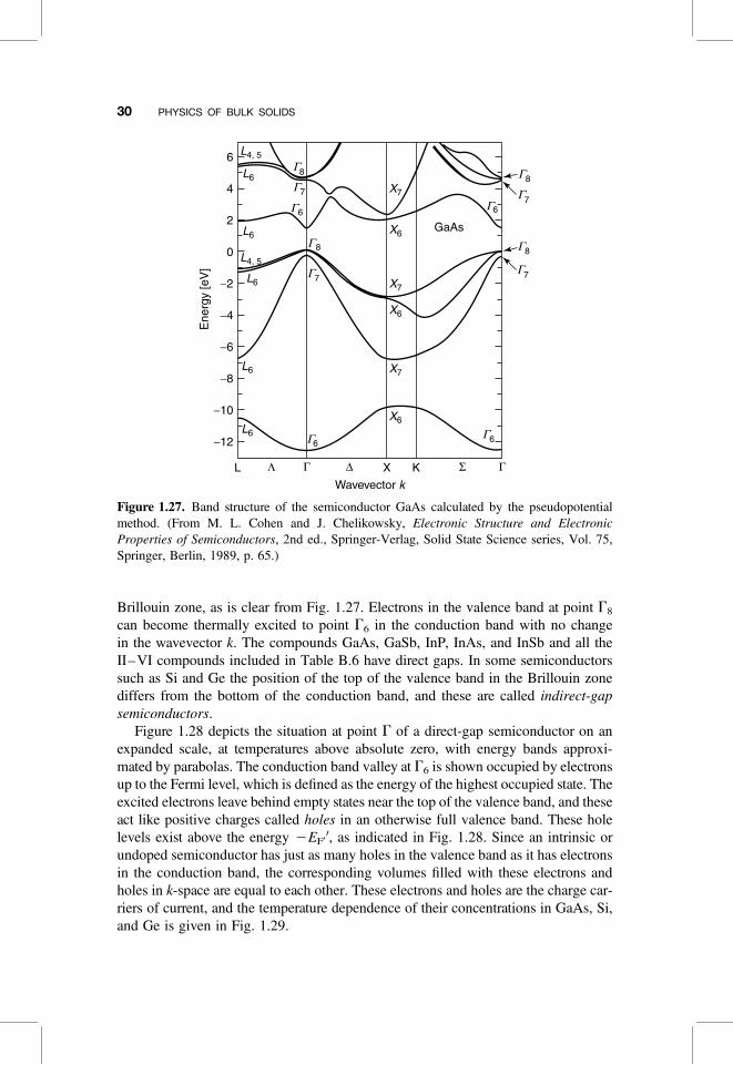
Brillouin zone, as is clear from Fig. 1.27. Electrons in the valence band at point G8
can become thermally excited to point G6 in the conduction band with no changein the wavevector k. The compounds GaAs, GaSb, InP, InAs, and InSb and all theII–VI compounds included in Table B.6 have direct gaps. In some semiconductorssuch as Si and Ge the position of the top of the valence band in the Brillouin zonediffers from the bottom of the conduction band, and these are called indirect-gapsemiconductors.
Figure 1.28 depicts the situation at point G of a direct-gap semiconductor on anexpanded scale, at temperatures above absolute zero, with energy bands approxi-mated by parabolas. The conduction band valley at G6 is shown occupied by electronsup to the Fermi level, which is defined as the energy of the highest occupied state. Theexcited electrons leave behind empty states near the top of the valence band, and theseact like positive charges called holes in an otherwise full valence band. These holelevels exist above the energy 2EF0
0, as indicated in Fig. 1.28. Since an intrinsic orundoped semiconductor has just as many holes in the valence band as it has electronsin the conduction band, the corresponding volumes filled with these electrons andholes in k-space are equal to each other. These electrons and holes are the charge car-riers of current, and the temperature dependence of their concentrations in GaAs, Si,and Ge is given in Fig. 1.29.
Figure 1.27. Band structure of the semiconductor GaAs calculated by the pseudopotentialmethod. (From M. L. Cohen and J. Chelikowsky, Electronic Structure and ElectronicProperties of Semiconductors, 2nd ed., Springer-Verlag, Solid State Science series, Vol. 75,Springer, Berlin, 1989, p. 65.)
30 PHYSICS OF BULK SOLIDS

Figure 1.28. Sketch of the lower valence band and the upper conduction band of a semicon-ductor approximated by parabolas. The region in the valence band containing holes and that inthe conduction band containing electrons are crosshatched. The Fermi energies EF and EF0
0
mark the highest occupied level of the conduction band and the lowest unoccupied level ofthe valence band, respectively. The zero of energy is taken as the top of the valence band,and the direct-bandgap energy Eg is indicated.
Figure 1.29. Temperature dependencies of the intrinsic carrier density of the semiconductorsGe, Si, and GaAs. (From G. Burns, Solid State Physics, Academic Press, Boston, 1985, p. 315.)
1.3. ENERGY BANDS 31
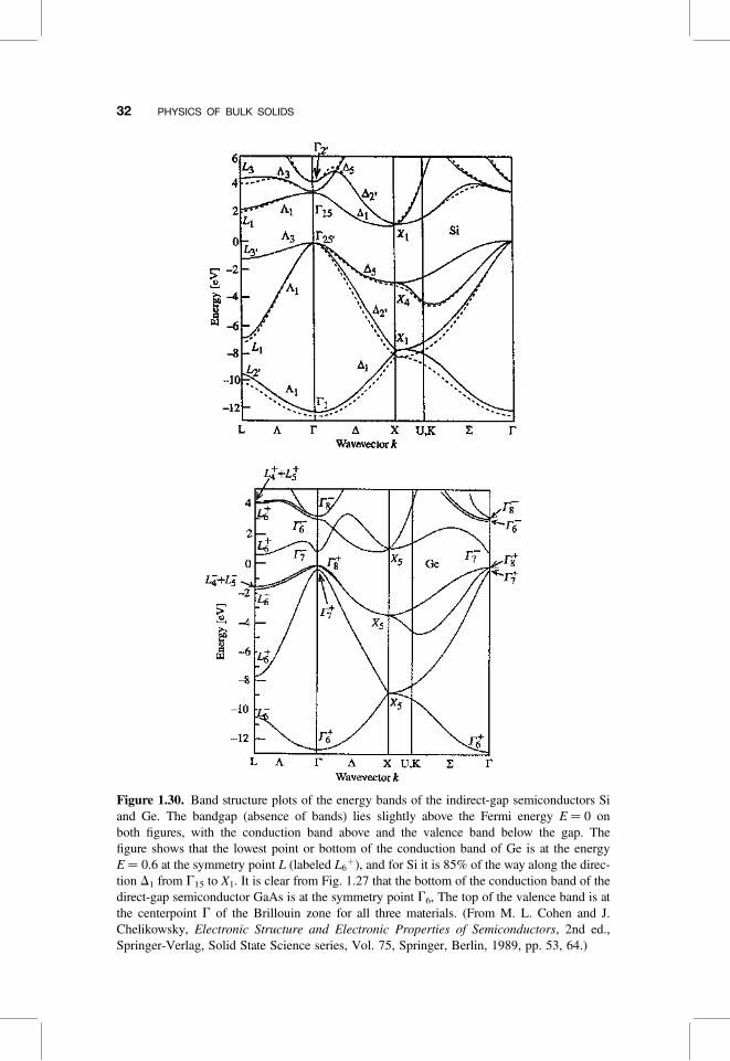
Figure 1.30. Band structure plots of the energy bands of the indirect-gap semiconductors Siand Ge. The bandgap (absence of bands) lies slightly above the Fermi energy E ¼ 0 onboth figures, with the conduction band above and the valence band below the gap. Thefigure shows that the lowest point or bottom of the conduction band of Ge is at the energyE ¼ 0.6 at the symmetry point L (labeled L6
þ), and for Si it is 85% of the way along the direc-tion D1 from G15 to X1. It is clear from Fig. 1.27 that the bottom of the conduction band of thedirect-gap semiconductor GaAs is at the symmetry point G6, The top of the valence band is atthe centerpoint G of the Brillouin zone for all three materials. (From M. L. Cohen and J.Chelikowsky, Electronic Structure and Electronic Properties of Semiconductors, 2nd ed.,Springer-Verlag, Solid State Science series, Vol. 75, Springer, Berlin, 1989, pp. 53, 64.)
32 PHYSICS OF BULK SOLIDS

In every semiconductor listed in Table B.6, including Si and Ge, the top of itsvalence band is located at the center of the Brillouin zone, but in the indirect-bandgap semiconductors Si, Ge, AlAs, AlSb, and GaP the lowest valley of their con-duction bands appears at different locations in k-space and at point G. This is shownin Fig. 1.30 for the indirect-bandgap materials Si and Ge. We see from Fig. 1.30 thatthe conduction band of Ge is minimum at point L, which is in the middle of the hex-agonal face of the Brillouin zone along the L or [111] direction depicted in Fig. 1.26.The Brillouin zone has eight such faces, with each point L shared by two zones, so thezone actually contains only four of these points proper to it, and we say that the valleydegeneracy for Ge is 4. The semiconductor Si exhibits a lowest conduction bandminimum along the D or [001] direction about 85% of the way to point X, asshown in Fig. 1.30. The corresponding valley of the compound GaP, not shown,also is located along D about 92% of the way to X. We see from Fig. 1.26 thatthere are six such D lines in the Brillouin zone, so this valley degeneracy is 6.Associated with each of the valleys that we have been discussing, at point L for Geand along direction D for Si, there is a three-dimensional constant-energy surfacein the shape of an ellipsoid that encloses the conduction electrons in the correspond-ing valleys, and these ellipsoids are sketched in Figs. 1.31a and 1.31b for Ge and Si,respectively.
Some interesting experiments such as cyclotron resonance have been carried outto map the configuration of these ellipsoid-type constant-energy surfaces. In acyclotron resonance experiment conduction electrons are induced to move along
Figure 1.31. Ellipsoidal constant energy surfaces in the conduction band of germanium (a)and silicon (b). The constant-energy surfaces of Ge are aligned along symmetry direction L
and centered at symmetry point L. As a result, they lie half inside (solid lines) and halfoutside (dashed lines) the first Brillouin zone, so this zone contains the equivalent of four com-plete energy surfaces. The surfaces of Si lie along the six symmetry directions D (i.e., along+kx, +ky, +kz), and are centered 85% of the way from the centerpoint G to symmetrypoint X. All six of them lie entirely within the Brillouin zone, as shown. Figure 1.26 showsthe positions of symmetry points G, L, and X, and of symmetry lines D and L, in theBrillouin zone. (From G. Burns, Solid State Physics, Academic Press, Boston, 1985, p. 313.)
1.3. ENERGY BANDS 33

constant-energy surfaces at a velocity that always remains perpendicular to an appliedmagnetic field direction. By utilizing various orientations of applied magnetic fieldsrelative to the ellipsoid, the electrons at the surface execute a variety of orbits, and bymeasuring the trajectories of these orbits, we can delineate the shape of the energysurface.
Table B.6 lists values of the energy gap Eg for types III–V and II–VI semicon-ductors at room temperature (left-hand value) and in several cases it also lists thevalue at absolute zero temperature (right-hand value). Table B.7 gives the temperatureand pressure dependences, dEg/dT and dEg/dP, respectively, of the gap at roomtemperature.
1.3.4. Effective Mass
The kinetic energy of a conduction electron moving at a velocity v in a semiconductoris found to have the value 1
2 m�v2 ¼ p2=2m�, where p ¼ m�v is the momentum, andoften the mass m� in these expressions differs from the electron’s fundamental or restmass value m0, which is a universal constant, so it is called an effective mass. This isanalogous to the case of the kinetic energy of an object of mass m moving at a velo-city v through a liquid. Its effective mass is reduced by the volume of the displacedliquid, and hence its measurable kinetic energy has a value lower than 1
2 mv2.On a simple one-dimensional model the energy E of a conduction electron has a
quadratic dependence on the wavevector k ¼ p/h through the expression
E ¼ h� 2k2=2m� (1:12)
The first derivative of this expression provides the velocity v
1h�
dE
dk¼ hk
m�¼ v (1:13)
and the second derivative provides the effective mass m�
1
h� 2
d2E
dk2¼ 1
m�(1:14)
which, as we said above, differs in general from the free-electron mass m0. Theseequations are rather trivial for the simple parabolic energy expression (1.12), butwe see from the energy bands of Figs. 1.27 and 1.30 that the actual dependence ofthe energy E on k is much more complex than Eq. (1.12) indicates. This equation(1.14) is a general definition of the effective mass m�, and the wavevector kdependence of m� can be evaluated from the band structure plots by carrying outthe differentiations. We see from a comparison of the slopes near the conductionband minimum and the valence band maximum of GaAs at point G on Fig. 1.27
34 PHYSICS OF BULK SOLIDS
(see also Fig. 1.28) that the upper electron bands have steeper slopes and hence lightermasses than do the lower hole bands with more gradual slopes.
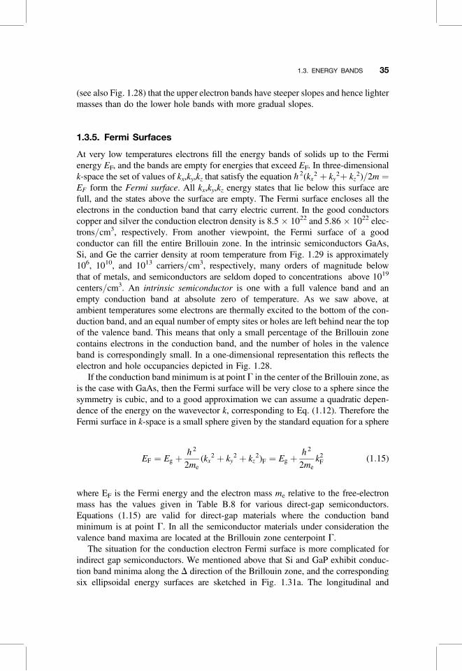
1.3.5. Fermi Surfaces
At very low temperatures electrons fill the energy bands of solids up to the Fermienergy EF, and the bands are empty for energies that exceed EF. In three-dimensionalk-space the set of values of kx,ky,kz that satisfy the equation h� 2(kx
2 þ ky2þ kz
2)=2m ¼EF form the Fermi surface. All kx,ky,kz energy states that lie below this surface arefull, and the states above the surface are empty. The Fermi surface encloses all theelectrons in the conduction band that carry electric current. In the good conductorscopper and silver the conduction electron density is 8.5 � 1022 and 5.86 � 1022 elec-trons/cm3, respectively. From another viewpoint, the Fermi surface of a goodconductor can fill the entire Brillouin zone. In the intrinsic semiconductors GaAs,Si, and Ge the carrier density at room temperature from Fig. 1.29 is approximately106, 1010, and 1013 carriers/cm3, respectively, many orders of magnitude belowthat of metals, and semiconductors are seldom doped to concentrations above 1019
centers/cm3. An intrinsic semiconductor is one with a full valence band and anempty conduction band at absolute zero of temperature. As we saw above, atambient temperatures some electrons are thermally excited to the bottom of the con-duction band, and an equal number of empty sites or holes are left behind near the topof the valence band. This means that only a small percentage of the Brillouin zonecontains electrons in the conduction band, and the number of holes in the valenceband is correspondingly small. In a one-dimensional representation this reflects theelectron and hole occupancies depicted in Fig. 1.28.
If the conduction band minimum is at point G in the center of the Brillouin zone, asis the case with GaAs, then the Fermi surface will be very close to a sphere since thesymmetry is cubic, and to a good approximation we can assume a quadratic depen-dence of the energy on the wavevector k, corresponding to Eq. (1.12). Therefore theFermi surface in k-space is a small sphere given by the standard equation for a sphere
EF ¼ Eg þh� 2
2me(kx
2 þ ky2 þ kz
2)F ¼ Eg þh� 2
2mek2
F (1:15)
where EF is the Fermi energy and the electron mass me relative to the free-electronmass has the values given in Table B.8 for various direct-gap semiconductors.Equations (1.15) are valid for direct-gap materials where the conduction bandminimum is at point G. In all the semiconductor materials under consideration thevalence band maxima are located at the Brillouin zone centerpoint G.
The situation for the conduction electron Fermi surface is more complicated forindirect gap semiconductors. We mentioned above that Si and GaP exhibit conduc-tion band minima along the D direction of the Brillouin zone, and the correspondingsix ellipsoidal energy surfaces are sketched in Fig. 1.31a. The longitudinal and
1.3. ENERGY BANDS 35
transverse effective masses, mL and mT, respectively, have the following values
mL
m0¼ 0:92
mT
m0¼ 0:19 for Si (1:16a)
mL
m0¼ 7:25
mT
m0¼ 0:21 for GaP (1:16b)
for these two indirect-gap semiconductors. Germanium has its band minimum at pointsL of the Brillouin zone sketched in Fig. 1.26, and its Fermi surface is the set of ellipsoidscentered at paints L with their axes along the L or [111] directions, as shown inFig. 1.31a. The longitudinal and transverse effective masses for these ellipsoids inGe are mL /m0 ¼ 1.58 and mT/m0 ¼ 0.081, respectively. Cyclotron resonancetechniques together with the application of stress to the samples can be used todetermine these effective masses for the indirect-bandgap semiconductors.
1.4. LOCALIZED PARTICLES
1.4.1. Donors, Acceptors, and Deep Traps
When an atom in column V of the periodic table, such as P, As, or Sb, which has fiveelectrons in its outer or valence electron shell, is a substitutional impurity in Si, it usesfour of these electrons to satisfy the valence requirements of the four nearest-neighborsilicons, and the one remaining electron remains weakly bound. The atom easilydonates or passes on this electron to the conduction band, so it is called a donor,and the electron is called a donor electron. This occurs because the donor energylevels lie in the forbidden region close to the conduction band edge by the amountDEd relative to the thermal energy value kBT, as indicated in Fig. 1.24. A Si atom sub-stituting for Ga plays the role of a donor in GaAs, Al substituting for Zn in ZnSe servesas a donor, and so on. The conductivity that is associated with the flow of electriccurrent carried by these conduction band electrons is called N-type.
An atom from column III atom such as Al or Ga, called an acceptor atom, whichhas three electrons in its valence shell can serve as a substitutional defect in Si, andin this role it requires four valence electrons to bond with the tetrahedron of nearest-neighbor Si atoms. To accomplish this it draws or accepts an electron from thevalence band, leaving behind a hole at the top of this band. The conductivitycorresponding to electric current carried by the movement of these holes is calledP-type. The transfer of an electron to Si occurs easily because the energy levels ofthe acceptor atoms are in the forbidden gap slightly above the valence band edgeby the amount DEA, which is small relative to kBT, as indicated in Fig. 1.24. Inother words, the excitation energies needed to ionize the donors and to add electronsto the acceptors are much less than the thermal energy at room temperature T ¼ 300 K(i.e., DED, DEA� kBT ), so virtually all donors are positively ionized and virtually allacceptors are negatively ionized at room temperature.
36 PHYSICS OF BULK SOLIDS

The donor and acceptor atoms that we have been discussing are known as “shallowcenters,” that is, shallow traps of electrons or holes, because their excitation energiesare much less than that of the bandgap (DED, DEA� Eg). There are other centerswith energy levels that lie deep within the forbidden gap, often closer to its centerthan to the top or bottom, in contrast to the case with shallow donors and acceptors.Since generally Eg kBT, these traps are not extensively ionized, and the energiesinvolved in exciting or ionizing them are not small. Examples of deep centers aredefects associated with broken bonds, or strain involving displacements of atoms.
1.4.2. Mobility
Another important parameter of a semiconductor is the mobility m or charge carrierdrift velocity v per unit electric field E, given by the expression m ¼ jvj/E. This par-ameter is defined as positive for both electrons and holes. Table B.9 lists the mobi-lities me and mh for electrons and holes, respectively, in the semiconductors underconsideration. The electrical conductivity s is the sum of contributions from the con-centrations of electrons n and of holes p in accordance with the expression
s ¼ (neme þ pemh) (1:17)
where e is the electronic charge. The mobilities have a weak power-law temperaturedependence Tn, and the pronounced T dependence of the conductivity is due princi-pally to the dependence of the electron and hole concentrations on the temperature. Indoped semiconductors this generally arises mainly from the Boltzmann factorexp(2Ei/kBT ) associated with the ionization energies Ei of the donors or acceptors.Typical ionization energies for donors and acceptors in Si and Ge listed in Table B.10range from 0.0096 to 0.16 eV, which is much less than the bandgap energies 1.12 eVand 0.67 eV of Si and Ge, respectively. Figure 1.24 shows the locations of donor andacceptor levels on an energy band plot, and makes clear that their respective ioniz-ation energies are much less than Eg. The thermal energy kBT ¼ 0.026 eV at roomtemperature (T ¼ 300 K) is often comparable to the ionization energies. In intrinsicor undoped materials the main contribution is from the exponential factorexp(2Eg/2 kBT ) in the following expression from the law of mass action
ni ¼ pi ¼ 2KkBT
2ph� 2
� �3=2
(memh)3=4 exp�Eg
2kBT(1:18)
where K is a constant and the intrinsic concentrations of electrons ni and holes pi areequal to each other because the thermal excitation of ni electrons to the conductionband leaves behind the same number pi of holes in the valence band, that is, ni ¼ pi.We see that the expression (1.18) contains the product memh of the effectivemasses me and mh of the electrons and holes, respectively, and the ratios me/m0
and mh/m0 of these effective masses to the free-electron mass m0 are presented in
1.4. LOCALIZED PARTICLES 37

Table B.8. These effective masses strongly influence the properties of excitons to bediscussed next.
1.4.3. Excitons
An ordinary negative electron and a positive electron, called a positron, situated a dis-tance r apart in free space experience an attractive Coulomb force, which has the value2e2/4p10r2, where e is their charge and 10 is the dielectric constant of free space. Aquantum-mechanical calculation shows that the electron and positron interact to forman atom called positronium, which has bound state energies given by the Rydbergformula introduced by Niels Bohr in 1913 to explain the hydrogen atom
E ¼ � e2
8p10a0n2¼ � 6:8
n2eV (1:19)
where a0 is the Bohr radius given by a0 ¼ 4p10h� 2/m0e2 ¼ 0.0529 nm, m0 is thefree-electron (and positron) mass, and the quantum number n takes on the valuesn ¼ 1,2,3, . . . ,4. For the lowest-energy or ground state, which has n ¼ 1, theenergy is 6.8 V, which is exactly half the ground-state energy of a hydrogen atom,since the effective mass of the bound electron–positron pair is half that of thebound electron–proton pair in the hydrogen atom. Figure 1.32 shows the energy
Figure 1.32. The first few energy levels in the Rydberg series of a hydrogen atom (a), posi-tronium (b), and a typical exciton (c).
38 PHYSICS OF BULK SOLIDS
levels of positronium as a function of the quantum number n. This set of energy levelsis often referred to as a Rydberg series. The continuum at the top of the figure is theregion of positive energies where the electron and the hole are so far away from eachother that the Coulomb interaction no longer has an appreciable effect, and the energyis all of the kinetic type, 1/2(mv2) ¼ p2/2m, or energy of motion, where v is the vel-ocity and p ¼ mv is the momentum.
The analog of positronium in a solid such as a semiconductor is the bound state ofan electron–hole pair called an exciton. For a semiconductor the electron is in theconduction band and the hole is in the valence band. The electron and hole bothhave effective masses me and mh, respectively, which are less than that m0 of a freeelectron, so the reduced mass mR is given by mR ¼ memh/(me þ mh). When theelectron effective mass is appreciably less than the hole effective mass, me�mh,the relationship between them is conveniently written in the form
mR ¼me
1þ (me=mh)(1:20)
which shows that for this case mR becomes comparable to the electron mass. Forexample, if me/mh ¼ 0.2, then m� ¼ 0.83 me. A comparison of the data inTable B.8 shows that this situation is typical for GaAs-type semiconductors. Wealso see from Table B.12 that the relative dielectric constant 1/10 has the range ofvalues 5.6 , 1/10 , 15.7 for these materials, where 10 is the dielectric constant offree space. Both of these factors have the effect of decreasing the exciton energyEex from that of positronium, and as a result this energy is given by
Eex ¼m�=m0
(1=10)2
e2
4p10a0n2¼ 13:6 m�=m0
(1=10)2n2eV (1:21)
as shown plotted in Fig. 1.32. These same two factors also increase the effective Bohrradius of the electron orbit, and it becomes
aeff ¼1=10
m�=m0a0 ¼
0:05291=10
m�=m0nm (1:22)
Using the GaAs electron effective mass and the heavy-hole effective mass valuesfrom Table B.8, Eq. (1.22) gives m�/m0 ¼ 0.058. Utilizing the dielectric constantvalue from Table B.11, we obtain, using Eqs. (1.21 and (1.22), for GaAs
E0 ¼ 4:5 meV, aeff ¼ 12:0 nm (1:23)
where E0 is the ground-state (n ¼ 1) energy. This demonstrates that an excitonextends over quite a few atoms of the lattice, and its radius in GaAs is comparablewith the dimensions of a typical nanostructure. An exciton has the properties of a
1.4. LOCALIZED PARTICLES 39
particle; it is mobile and able to move around the lattice. It also exhibits characteristicoptical spectra. Figure 1.32 plots the energy levels for an exciton with the ground-state energy E0 ¼ 18 meV.
Technically speaking, the exciton that we have just discussed is a weakly boundelectron–hole pair called a Mott–Wannier exciton. A strongly or tightly boundexciton, called a Frenkel exciton, is similar to a longlived excited state of an atomor molecule. It is also mobile, and can move around the lattice by the transfer ofthe excitation or excited-state charge between adjacent atoms or molecules. Almostall the excitons encountered in semiconductors and in nanostructures are of theMott–Wannier type, except in organic nanocrystals, where they are Frenkel excitons.
PROBLEMS
1.1. Find the volume and the surface area of the cuboctahedron sketched in Fig. 1.6.
1.2. Consider a nanofilm formed from the two-dimensional close-packed lattice ofFig. 1.4. The smallest n ¼ 1 nanofilm is, of course, one atom, and the n ¼ 2one is the seven-atom (N ¼ 7) structure sketched on the left side of Fig. C.1of Appendix C. The number of atoms around the edge is given by Nedge¼
6(n 2 1) valid for n . 1, in analogy with Eq. (1.4). Make accurate sketchesof the n ¼ 3, n ¼ 4, and n ¼ 5 planar nanoparticles, and prepare the analog ofTable 1.3 for this two-dimensional case for n values ranging from 1 to 5.
1.3. Evaluate the coefficients A, B, and C of the equation N ¼ An2 þ Bn þ C for thenumber of atoms in a two-dimensional nanoparticle.
1.4. Find the distances between [111] planes of the zinc blende lattice in terms of thecubic unit cell dimension a for the following cases: (a) two nearest sulfur planes,(b) two nearest zinc planes, and (c) adjacent S and Zn planes. Why are there twoanswers for case (c)?
1.5. Consider three fcc nanoparticles containing approximately 1000 atoms: one inthe shape of an octahedron, one in the shape of a cube, and one in the shapeof the structure depicted in Fig. 1.9. Which has the largest, and which has thesmallest value of surface energy per unit volume? What are their values?
1.6. A two-dimensional close packed lattice of circular atoms is illustrated inFig. 1.4a. What is the radius of the interstitial sites of this lattice, and hownumerous are they compared to the atoms?
1.7. A square of side a has zero-dimensional apices, four one-dimensional edges, andone two-dimensional face. If the square is projected out into the third dimensionand the vertices of the two squares are connected with straight lines of length a, theresulting three-dimensional cube has 8 vertices, 12 edges, and 6 faces. Considerprojecting the cube out into a fourth dimension and connecting the respective ver-tices with straight lines of length a, to form a four-dimensional “cube” called atesseract. How many apices, edges, faces, and cubes does the tesseract have?
40 PHYSICS OF BULK SOLIDS

REFERENCES
1. N. W. Ashcroft and N. D. Mermin, Solid State Physics, Saunders College, Philadelphia,1976.
2. G. Burns, Solid State Physics, Academic Press, San Diego, 1985.
3. C. Kittel, Introduction to Solid State Physics, 7th ed., Wiley, New York, 1996.
4. P. Y. Yu and M. Cardona, Fundamentals of Semiconductors, 3rd ed., Springer-Verlag,Berlin, 2001.
5. T. P. Martin, T. Bergmann, H. Gohlich, and T. Lange, Chem. Phys. Lett. 172, 209 (1990).
6. S. Sugano and H. Koizumi, Microcluster Physics, Springer, Berlin, 1998, p. 90.
7. C. P. Poole, Jr. and H. A. Farach, Chemical Bonding in Semiconductor Physics, K. Boer,ed., Wiley, New York, 2001, Vol. 1, Chapter 2.
REFERENCES 41