chamber pcb s, feb s, cooling, hv/lv distribution 1)pcb designs-track widths, track to track...
TRANSCRIPT

Chamber PCB s, FEB s, Cooling, HV/LV Distribution
1) PCB designs-track widths, track to track distances …
2) Double sided and Multi layer, modular approach.
3) Resistors for protection against possible sparks.
4) Orientation of FEB s, Scheme, Cooling
5) HV/LV distribution- No of channels, Modules, cost

Prototype PCBs
No of pads- 256, Pad sizes-8*3.4 sq mmReadout area-97*85 Sq mm. Read by 2 FEBs each with 128 channels.2 types of pad sizes tried. Both Staggered. Double sided PCB
Track widths -6milTrack- track – 6 mil to 15mil.Resistors added later (0603)
Top copper
256 tracks - all on bottom copper
For previous test beams
vias from- top to bottom copper

For next Test beam
Resistors -0402
3 and 4 sq mm pads. Not staggered.
Track lengths are long.
4 mil tracks. Track- track 4 /6 mil spacing Cross talk??? Multi layer with GND planes???
512 pads- to be read by 4 FEBs each 128 channels
Double sided PCB- all 512 tracks on bottom copper only
Bottom copper
Top copper
Pad area-67*73 Sq mm for 3mm. For 4mm - 88*97 sq mm

4 layer PCB with GND PlaneTop copper
Inner 1
Inner 2
Bottom copper
Connectors for FEBsConnector with resistors
Type 1
GND Plane
GND plane
GND Plane
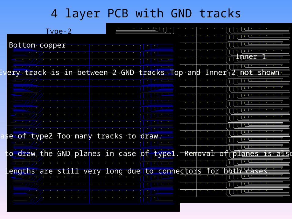
4 layer PCB with GND tracks
Bottom copper
Inner 1
Every track is in between 2 GND tracks.
in case of type2 Too many tracks to draw. Easy to draw the GND planes in case of type1. Removal of planes is also easier
Track lengths are still very long due to connectors for both cases.
Type-2
Top and Inner-2 not shown.

Modular approachInner 1 Inner-2 Bottom Copper 2.6 Sq mm Pads
32*8 matrix. 256 pads Single 300 pin Connector. Reads 2 n - XYTERS.
Top copper
Blind vias from inner layers( blue)
Blind vias (red ) to inner layer
2.6 mm square pads
Pads arranged in one block of 32*8=256.
Connected to 300 pin connector.
Tracks - shorter and not closer . can be easily duplicated for bigger sizes. 4 such blocks for GEM of 10cm * 10 cm.
Each block read by 1 FEB with 2 n-XYTERs
No resistors could be added so far.
FEBs can be mounted horizontal or vertical
For STAR PMD
For ALICE PMD

Prototype design
Inner1
Inner2
Bottom copper
Top copper
4 connectors. Each reads 2 N-XYTERS.
44 spare pins on the connector.

FEB--Probable scheme??
64 channel chip-- No of Pin outs 125-150?
For inputs- 64 For I2c - 6For CLK - 6For SDA, SCl - 2I2C Reset - 2Reset 2 DATA (diffl) --- 18 ( 16 for digital, 2 analog)
Total -100 PLUS Bias ,GND, other control inputs -25 to 50 ??
Consider
BGA144(1,27mm pitch) / SQFP148(10*14)
with 148 pin count and if we arrange-see the board size-10cm*3.2cm
BGA-144
ADC
300 Pin CON
SQFP148
ADC
ROC CON

Cooling Issues
FEB with one NXYTER draws 1.5A @5V.(with regulators)
For a 2 chip FEB , Current drawn is expected to be 3A minimum. Power= 15Watts. With 3.3V it is 10 Watts.
With 4 such FEBs, each reading a zone with 1K pads, the power dissipation is 40 Watts on an area of 10(cm) * 10 (cm).
Same as power dissipated on one ALICE-PMD module (4608 cells).
Each FEB with 2/4 n –XYTERS needs cooling. To be taken care while designing the FEB.

Detector specifications
Detector active area= 20 sq met. GEM PCB dimensions= 30x30Cm. No Of GEMS required =20 ÷0.3x0.3= 222.2= 222
Total number of GEMs required = 222x3= 666 (for triple GEM).
9k pads on one chamber PCB (30cm by 30 cm) For 500,000 we need 56 Nos, each for chamber and drift PCBs (min).
HV
HV channels required for GEM PCBs = 222 ( one for each triple GEM)
HV specification = 3 to 5 KV/1mA /5Watts.
CAEN 1535 board has 24 HV channels. Each = 3.5KV/3mA. SHV /multi pin connectors.CAENA1550-5KV/1mA with multi Pin and SHV
Can be housed in SY1527. Number of boards required will be = 10 ( 10x24=240 channels).
SY 1527 houses 5/10 boards. Need 2/1 Crates. Power consumption= 240x5Watts = 1.2KW
Detector, HV

FEBs-LV FEB s, ROC s
Channels to read= 500,000
One N-XYTER reads =128 channels. FEB with 2 n-XYTERS reads-256 channels
No of FEB s Required = 500,000÷256 = 2000 No (512,000 channels).
Each ROC can handle = 2 FEBs (512 channels). No Of ROCs required =1000Nos.
LV Specifications
2chip Feb With 3.3 v supply the power dissipation =10watts.
2000 FEBs consume =2000x 10Watts =20KW.
One ROC need -3.5A @5V ( one FEB connected). With two FEBs it is 4A
1000 ROC s consume = 1000x5Vx4A=20KW.
Power consumption expected for 2000FEBs +1000 ROCs = 40KW

A3009B -2to 8 V, 9A @5V. Max =45W. Has 12 independent channels. Max 480Watts
For 1000 ROCS Need 1000÷12= 84 modules
For 2000 FEBSs = 2000÷12= 167 modules. Need 167+84 =251 modules. Separate LV channels for FEB and ROC. Alternately:
Reduce LV channels to 168÷2=84 by using LVDB to feed 2 FEBS (from 1 channel)
Need 84+84 =168 modules.
No of 3009s in one EASY crate =4 (2KW)
EASY crates Required = 250÷4=63 or 164 ÷4=41
With 2 channels 3486 has =48V /40A , Power Capacity =5KW
3486 s required = 40KW÷5 = 8Nos. Filter for 3486 =8 Nos. One Branch Controller (A1676A) controls 6 EASY- 3000 Crates.
For 63/41 Crates we need = 11 /7 Branch controllers
.
LV distribution

Costs of CAEN-LV/HV modules
• SY1527 -Universal Crate-- 11K Euro• 3486-48V supply- 12K Euro• A3000NF-Filter for 3486--- 3.2KEuro• A1676- Branch Controller --- 1.4K Euro• A3009B--- 2 to 8V supply ----- 7.1K Euro• EASY 3000 Crate (for A3009B)---- 2.6K Euro• A1535-24 channel HV module---- 4.8K Euro• A1550 -24 Channel HV module---------- 5.8K Euro

Issues to be taken care
Too many modules and Crates ???
Alternate systems from WEINER or ??
Which Detector Control System PVSS or ??? Cooling system - water cooled or air cooled??
FEB PCB vertical type of horizontal type ???
If No regulators on the FEB, any precaution to be taken in DB…..????