california state university northridge electrical
TRANSCRIPT

CALIFORNIA STATE UNIVERSITY NORTHRIDGE
ELECTRICAL ENGINEERING FUNDAMENTALS LABORATORY EXPERIMENTS 1-12
ELECTRICAL ENGINEERING ECE 240L
LABORATORY MANUAL
Prepared By: Benjamin Mallard
Department of Electrical and Computer Engineering
(Revised 12/11)

1
Introduction
The main objective of this manual is to relate the theory of circuit analysis and practice.
Each laboratory experiment consists of the "equipment needed", theory, preliminary
calculations and procedure. Students are required to review the theory and complete
the preliminary calculations before the lab period and perform the actual experiment.
The theory is presented in brief and is to assist students with basic equations and in-
formation needed to complete the calculations and perform the measurements. The last
experiment in this manual is optional. It is intended for students to gain design expe-
rience in using the theories, practices, and measurement techniques used in the prior
experiments.

2
ECE 240 EXPERIMENTS
1) LABORATORY INSTRUMENTS AND REPORTS
2) OSCILLOSCOPES
3) DC CIRCUITS
4) COMPUTER SIMULATION
5) NETWORK THEOREMS
6) OPERATIONAL AMPLIFIERS
7) FIRST ORDER CIRCUITS
8) SECOND ORDER CIRCUITS
9) IMPEDANCE AND ADMITTANCE
10) FREQUENCY RESPONSE
11) PASSIVE FILTERS
12) DESIGN EXPERIMENT

3
EXPERIMENT ONE LABORATORY INSTRUMENTS AND REPORTS
1) EDUCATIONAL LABORATORY VIRTUAL INSTRUMENTATION SUITE (ELVIS) 2) BREADBOARD STRUCTURE AND LAYOUT 3) POWER SUPPLIES 4) GROUNDING 5) DIGITAL MULTIMETERS 6) OSCILLOSCOPES 7) FUNCTION GENERATORS 8) LABORATORY REPORTS
ELVIS FEATURES AND LAYOUT Insert the Prototyping Board (breadboard) into slots on top of the Benchtop Worksta-tion. Find and identify the following features on the Benchtop Workstation (Front Panel): 1) Prototyping Board Power Button 2) System Power Indicator Light 3) Communications Bypass/Normal Switch 4) Variable Power Supply Switches and Knobs 5) Function Generator:
i) Manual Select Switch ii) Waveform Select Switch iii) Frequency Select Knob iv) Fine Frequency Adjustment Knob v) Amplitude Adjustment Knob
6) Digital Multimeter (DMM):
i) Input Current Measurement Terminal (HI) ii) Input Current Measurement Terminal (LOW) iii) Input Voltage Measurement Terminal (HI) iv) Input Voltage Measurement Terminal (LOW)

4
7) Oscilloscope (SCOPE): i) Channel A Input (CH A) ii) Channel B Input (CH B) iii) External Trigger Input (TRIGGER)
Find and identify the following features on the Prototyping Board: 1) Analog Pins:
i) Differential Analog Inputs (6) ii) Analog Sense Input iii) Analog Ground
2) Oscilloscope Pins:
i) Oscilloscope Signal Inputs ii) Oscilloscope Trigger Input
3) Programmable Function Pins:
i) Programmable Functions Inputs (5) ii) Scan Clock (Scanclk) iii) Reserved (External Strobe Pin)
4) Digital Multimeter (DMM) Pins:
i) 3 Wire Transistor Measurements (3-Wire) ii) Input Current Measurement Pin (+) iii) Input Current Measurement Pin (-) iv) Input Voltage Measurement Pin (+) v) Input Voltage Measurement Pin (-)
5) Analog Outputs (2)
i) DAC0 ii) DAC1
6) Function Generator
i) Output Signal (FUNC_OUT) ii) Synchronization Signal (SYNC_OUT) iii) Amplitude Modulation Input (AM_IN) iv) Frequency Modulation Input (FM_IN)

5
7) User Configurable I/O (8): i) Banana Connector A (BANANA A) ii) Banana Connector B (BANANA B) iii) Banana Connector C (BANANA C) iv) Banana Connector D (BANANA D) v) BNC Signal 1 (BNC 1+) vi) BNC Signal 1 Ground or Reference (BNC 1-) vii) BNC Signal 2 (BNC 2+) viii) BNC Signal 2 Ground or Reference (BNC 2-)
8) Variable Power Supplies:
i) Positive Output of 0V to 12V (SUPPLY+) ii) Power Supply Ground or Common (GROUND) iii) Negative Output of 0V to 12V (SUPPLY-)
9) DC Power Supplies:
i) Fixed +15V Output (+15V) ii) Fixed -15V Output (-15V) iii) Power Supply Ground or Common (GROUND) iv) Fixed +5V Output (+5V)
Although there are more features on the Prototyping Board, the connections, pins, and terminals listed above are the only items of importance for the ECE240 Laboratory.

6
BREADBOARD STRUCTURE AND LAYOUT
Figure 1.1
+ -
A B C D E F G H I J
+ -
+
-
5
10
15
20
25
30
35
40
45
-
+
I II III

7
The diagram shown on the previous page is that of the circuit construction area on the prototyping board. In the laboratory, this area is used to construct a preliminary circuit according to the circuit schematic or wiring diagram. An explanation on its use is as follows. SECTIONS I and III The holes in these sections are connected vertically. Moreover, the column of holes between the ‘+’ signs are connected. These are the holes adjacent to the red vertical stripe. Likewise the holes located between the ‘-’ signs are connected. These holes are adjacent to the vertical blue line. There is no electrical connection of these holes hori-zontally. It is suggested that the holes in this section be reserved for direct connections to laboratory equipment. This enables the user to distributed common connections throughout the circuit that is suggestively constructed in section II. SECTION II The holes at this location are electrically connected horizontally. Each row of holes is connected on each side of the groove or trough. The groove isolates one row of holes from the other horizontally. There is no electrical connection of any of these holes in the vertical direction. Each column of holes in this section is not connected. Since there are more holes in this section, construction of the circuit to be analyzed or de-signed is reserved for this area.

8
Electrical components are placed in holes where other connections can be made. An example is shown below.
Figure 1.2
+
+
-
-
A B C D E F G H I J
+ -
+
-
5
10
15
20
25
30
35
40
45
R1
R2
to COM Of Power Supply
from +6V terminal of Power Supply

9
Schematic (circuit diagram) A schematic is a drawing of a circuit comprised of symbols and lines representing the connection scheme. In figure 1.3, the circuit connection shown in figure 1.2 is illu-strated.
Figure 1.3 Circuit Layout The diagram shown below depicts what is called a circuit layout. This type of diagram shows physical components, the terminals associated with them, and a wiring scheme showing how each component of the circuit is connected. In the diagram below, the triple power supply is connected in series with resistors R1 and R2. This depiction is the associated circuit layout of the circuit shown schematically above in figures 1.2 and 1.3. The series loop terminates on the COM (ground) terminal of the power supply thus completing the circuit. All power supplies have a “power on” switch that allows electricity to flow into the com-ponent from the wall or bench supply. Locate this switch and become familiar with its locality. The power supply also has indicator lights, LEDs, and numerical displays which provide information regarding over voltage and short circuit current protection, and values of dialed voltage and current respectfully. Locate these features and be-come familiar with them.
CO
R2
R1
6

10
Figure 1.4 GROUNDING The concept of grounding is quite simple. Although some may think grounding is a concept whereby a path is chosen for electrons (or charge carriers in general) to dis-appear into the physical or earth ground, nothing is farther from the truth. The ground point in any circuit is a reference point or connection from which all voltages are meas-ured. The ground node in a circuit by convention has a voltage of zero. Therefore the voltage measured at any other node registers a measurement of the voltage “differ-ence” from that node to the reference or ground node. In establishing the ground node in a circuit, typically this node is located at the power source of the circuit. On all power supplies this is labeled as the COM socket or con-nector as mentioned previously. After the ground node has been designated in a cir-cuit schematic, this node should physically be the COM connection on the power supply of the circuit. If more than one power supply is used, then all COM connectors of each power supply should be connected together.
+6V +20V -20V COM
VOLTS AMPS
TRIPLE POWER SUPPLY
R1 R2

11
PROCEDURE
1. Turn the power supply off. Make sure there is nothing connected to the output voltage terminals.
2. Connect one banana lead to the +6V output of the power supply and the other
end to the voltage input of a digital multimeter. Connect another banana lead to the COM terminal of the power supply and the other end to the COM terminal of the digital multimeter.
3. On the power supply, turn all voltage adjustment knobs all the way to the left.
4. Turn on the power supply and digital multimeter. Make sure the voltage display
on the power supply and the digital multimeter reads approximately 0 volts. The amp display on the power supply should read 0 amps.
5. Slowly turn the voltage adjustment knob to the right until the digital multimeter
displays +6V.
6. Turn the power supply off.
7. Connect the power supply to the circuit illustrated in the circuit diagram above. Make sure the COM terminal of the power supply is connected to R2.
8. Turn on the power supply.
9. Measure voltages using the digital multimeter at each resistor lead and record
them.
10. Turn off the power supply.
11. Repeat steps 1 through 10 with power supply voltage outputs of +5V, +3V, and +1V.
12. Turn on the computer and select the NI ELVIS icon.
13. From the NI ELVIS menu on the monitor, select the DIGITAL MULTIMETER.
14. Turn off the Benchtop Workstation power supply. Verify that the power indicator
light is off. Connect a wire from the 0V to 12V (SUPPLY+) output pin of the pro-totype board to the HI input voltage measurement pin of the digital multimeter. Connect another wire from the Power Supply Ground or Common (GROUND) pin of the prototype board to the LOW input voltage measurement pin of the digital multimeter.
12
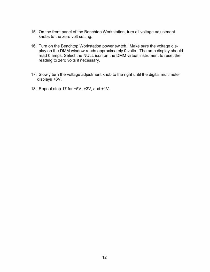
15. On the front panel of the Benchtop Workstation, turn all voltage adjustment
knobs to the zero volt setting. 16. Turn on the Benchtop Workstation power switch. Make sure the voltage dis-
play on the DMM window reads approximately 0 volts. The amp display should read 0 amps. Select the NULL icon on the DMM virtual instrument to reset the reading to zero volts if necessary.
17. Slowly turn the voltage adjustment knob to the right until the digital multimeter
displays +6V. 18. Repeat step 17 for +5V, +3V, and +1V.

13
DIGITAL MULTIMETER The digital multimeter or DMM is used to measure electrical quantities of voltage, cur-rent, and resistance. For voltage and current, the meter measures both DC and AC quantities. For AC voltages and currents, the meter measures what is typically called RMS quantities. These measurements are internally calculated by the meter using the following formulas for sinusoidal voltages and currents.
1.12
,2
PRMS
PRMS
II
VV
VP is the peak voltage and IP is the peak current of an AC waveform or signal.
Resistance is measured in units of ohms and kilohms. The following procedure ex-plains how these measurements should be performed.
1. Insert one banana lead into the volt/kΩ socket on the front of the multimeter. In-
sert another banana lead into the COM socket.
2. Place alligator clips on the ends of both leads and connect them to opposite leads of the resistor to be measured.
3. Select the kΩ measurement push-in button on the front of the multimeter.
4. Beginning with the scale selected at the lowest range of measurement, push in
the scale buttons until a stable reading appears on the display.
5. Record the measurement. Measuring resistance using the ELVIS is performed as fellows:
1. Place the resistor to be measured into an appropriate pair of holes on the proto-typing board.
2. Connect a wire from one lead of the resistor to the + input current measurement
pin. Connect another wire from the other lead of the resistor to the – input cur-rent measurement pin.
3. In the DMM window of the ELVIS software, select the ohmmeter measurement
feature.
4. Using the measurement scale selection, find the setting that provides the largest resolution as possible.
5. Record the measurement.

14
OSCILLOSCOPES The oscilloscope is a laboratory instrument that allows viewing of time-dependent signal voltages. Each bench is supplied with an analog and a digital oscilloscope. The analog oscilloscope provides a visual representation of a signal on a voltage versus time axis. This axis is viewed on the display portion of the instrument. From this display, the experimenter is able to measure parameters such as:
Peak voltage Frequency Period of oscillation Time constants Phase angle The digital oscilloscope allows the user to measure the same quantities with the added bonus of selected menus that automatically measure and display them as well. The following procedure allows the user to become familiar with these fea-tures. ANALOG OSCILLOSCOPE
1. Locate the power button and turn it on.
2. Locate the two channel modules on the oscilloscope (channel 1 and channel 2).
3. On both channels, select the ground reference position.
4. Observe the Voltage Sensitivity knobs for channel 1 and channel 2. Record
the settings for each knob position.
5. Locate the Time Base module. Record the settings for each knob position.

15
DIGITAL OSCILLOSCOPE
1. Locate the power button and turn it on.
2. Locate the two channel modules on the oscilloscope (channel 1 and channel 2).
3. On both channels, select the ground reference position.
4. Observe the Voltage Sensitivity knobs for channel 1 and channel 2. Record
the settings for each knob position.
5. Locate the Time Base module. Record the settings for each knob position.
6. Locate and observe the menu buttons on the right side of the oscilloscope. Record the different options for each button.
On the ELVIS, select the OSCILLOSCOPE virtual instrument and perform the same steps described for the DIGITAL OSCILLOSCOPE.

16
FUNCTION GENERATORS
Like the power supply, function generators are also a voltage source for any pas-sive circuit. In order to see the output voltages from the function generator an oscil-loscope must be used. The following are knobs on the function generator which provide certain functions. Amplitude – peak voltage of the output waveform Frequency – periodicity of the output waveform Sine – sine waveform Square – square waveform Triangular – triangular waveform Offset – DC bias level Multiplier – frequency range selector
1. Connect a double BNC cable to the OUT terminal of the function generator and the other end to the channel 1 input on the oscilloscope.
2. Turn on the function generator and the oscilloscope.
3. Select the SINE waveform on the function generator.
4. Adjust the AMPLITUDE and FREQUENCY knobs on the function generator
until a sine wave appears on the oscilloscope screen.
5. Turn the OFFSET knob on the function generator and record your observa-tion.
6. Select different MULTIPLIER settings on the function generator and record
your observation.
Repeat steps 1 through 6 selecting the SQUARE and TRIANGULAR waveforms. On the ELVIS system, select the FUNCTION GENERATOR virtual instrument and per-form the same steps as listed above.

17
LABORATORY REPORTS The laboratory report is the most important document in this class. The contents of this report should not only tell the reader what the experimenter did, but also allow the reader to duplicate the experiment in complete detail. The aim of the laboratory report is to provide information into the examination of a theory or formula in order to confirm its validity or to expose deviations from its exactness. In addition it also contains details on the process of experimentation. A generic structure is presented here as a guide to help the student develop sound investigative reporting skills. INTRODUCTION All reports should begin with an introduction that describes what the experiment is about and why certain items are being investigated (e.g. – Ohm’s Law, Thevenin’s Theorem, etc.). It should be stated here what the outcome or results of the experiment would be. This section should only be a few sentences which should be written in a manner to interest or entice the reader to peruse the document. PROCEDURE(S) or METHOD(S) The student should use his or her own words in this section to describe the strategy of how the experiment or investigation was performed. In this section a brief history may be included to educate the reader on what past procedures were used to conduct the same or similar experiments. This section of the report should also include a list of ma-jor lab equipment that was used in the experiment. Circuit schematics or diagrams, connection layouts including equipment, is also useful in describing how an item was tested or examined. RESULTS and/or OBSERVATIONS This section should be the most voluminous part of the report. It is extremely important to relate and document every measurement and observation here. To organize these data tables, charts, graphs, etc. may be used. Software tools such as spreadsheets and data bases are commonly used but not required. DISCUSSION This is the section where the student earns his or her grade essentially. Here the components of the previous section are explained, validated, or not. It is very impor-tant for the student to express his or her true thoughts on how the experiment provided added knowledge into the field of electrical engineering or not. If the results are erro-neous, provide reasons/justifications for errors and state how to produce the correct results. CONCLUSION This section can be combined with the previous section if desired. It is meant to pro-vide a summary of the outcome and results of the experiment in order to leave a last impression on the reader.

18

19
EXPERIMENT TWO OSCILLOSCOPES
EQUIPMENT NEEDED: 1) Analog Oscilloscope 2) Function Generator 3) Resistors 4) ELVIS
THEORY AND PRELIMINARY PREPARATION Review the oscilloscope exercises from experiment 1. Your instructor will give a brief lecture on the use of the analog, digital, and ELVIS oscilloscopes. Procedure 1) Set the frequency dial of the function generator to 1 kHz. Push the waveform select
button to output a sine wave. Display the sine wave on channel 1 of the analog os-cilloscope. Set the voltage sensitivity to 5V/DIV. Adjust the amplitude knob on the function generator to produce a 2 volt peak (4 volts peak-to-peak) waveform on the oscilloscope.
a) Sketch the display to scale after setting the time base on the oscilloscope to 1
ms/div, 0.1ms/div, and 10µs/div. Be sure to label the voltage and time axes with accurate divisions.
b) Set the time base on the oscilloscope so that one or two cycles of the sine wave
is visible. Measure the period of the waveform. Record this as Tmeas. Calculate
the frequency of oscillation. Record this as fmeas. Compare this calculation with
the frequency setting of the function generator.
c) Calculate the percentage error between the frequency setting of the function
generator fdial, and fmeas using the following formula:
1.2%100%
dial
dialmeas
f
fferror
d) Measure the voltage of the sine wave using the digital multimeter. Connect the
sine wave output to the AC voltage input of the digital multimeter. Record this measurement as the RMS voltage of the sine wave.

20
e) From the results of part d, calculate the conversion factor K using the following formula:
2.2RMS
peak
V
VK
2) Repeat all of step 1 for a 2V peak, 1 kHz square wave. 3) Construct the circuit shown in figure 2.1. Using the analog oscilloscope, set the
sensitivity knobs on channels one and two to the same setting. Select the display mode setting of X-Y. Connect VL to channel two and VS to channel one.
a) Sketch the display to scale. b) From the straight line displayed on the oscilloscope, measure the slope m.
c) Calculate the theoretical value of m using the following formula: S
L
V
Vm
Figure 2.1
2V, peak
+
GND (Common)
x - input
to scope
4.7kΩ 1kHz
+
-
10kΩ
- y - input
to scope vs vL

21
EXPERIMENT THREE
DC CIRCUITS
EQUIPMENT NEEDED:
1) DC Power Supply 2) DMM 3) Resistors 4) ELVIS
THEORY
Kirchhoff's Laws:
Kirchhoff's Voltage Law: The algebraic sum of the voltages around any closed path
is zero.
N
i
iv1
1.30
Kirchhoff's Current Law: The algebraic sum of the currents at any node is zero.
N
i
ii1
2.30

22
Series Circuits:
In a series circuit the current is the same through all the elements.
Figure 3. 1
The total series resistance RS is given by
3.3121 NNS RRRRR
and
4.3SS IRV
The Kirchhoff's voltage law indicates that:
5.3121 NNS VVVVV
V
R
+ V1 -
R
+ V2 -
R
- VN + - VN-1 +
RN-
I

23
The voltages across resistors can be obtained by multiplying the current by the corresponding
resistors.
6.3
11
22
11
11
22
11
S
S
NN
S
S
NN
S
S
S
S
S
S
NN
NN
VR
RV
VR
RV
VR
RV
VR
RV
R
VI
IRV
IRV
IRV
IRV
The last expressions of equation 3.6 are known as voltage division.

24
Parallel Circuits:
In a parallel circuit the voltage is the same across all the elements.
Figure 3. 2
The total parallel resistance, Rp is given by
7.311111
121 NNP RRRRR
and
8.3PPP RIV
Kirchhoff's current law states:
9.3121 NNP IIIII
I RI RI RN-IN- RI PV P
+
-

25
The current through the branch resistors can be obtained by dividing the terminal voltage PV
by the corresponding branch resistance, R. therefore:
10.3
1
1
2
2
1
1
1
1
2
2
1
1
P
N
PN
P
N
PN
PP
PP
PPP
N
PN
N
PN
P
P
IR
RI
IR
RI
IR
RI
IR
RI
RIV
R
VI
R
VI
R
VI
R
VI
The last expressions of equation 3.10 are known as current division.
The reciprocal of resistance is known as conductance. It is expressed in the following equa-
tions:
11.31
RG
and
12.31
PP
RG

26
This expression can be used to simplify equations 3.12 as shown below.
13.3
11
22
11
11
22
11
PP
NN
PP
NN
PP
PP
P
PP
PNN
PNN
P
P
IG
GI
IG
GI
IG
GI
IG
GI
G
IV
VGI
VGI
VGI
VGI
where
14.31111
121 NNP
RRRRG

27
If only two resistors make up the network, as shown next
Figure 3.3
then the current in branches 1 and 2 can be calculated as follows:
18.31
17.311
16.31
15.3
21
21
21
21
11
21
21
21
11
11
PP
PP
PP
IRR
RII
RR
RR
RI
RR
RRG
RRG
and
RG
IG
GI
In a similar fashion it can be shown that
19.321
12 PI
RR
RI
(Note how the current in one branch depends on the resistance in the opposite branch)
R1 I1
R2
I2
IP

28
But, if the network consists of more than two resistors - say four
Figure 3.4
Then the calculation or branch currents using individual resistance becomes complex as
demonstrated next, e.g.,
21.3111111
20.3
4321
321421431432
4321
3
3
RRRR
RRRRRRRRRRRR
RRRRRR
IR
RI
PP
PP
so that
22.31
321421431432
4321
3
3 PIRRRRRRRRRRRR
RRRR
RI
and
23.3321421431432
4213 PI
RRRRRRRRRRRR
RRRI
R3
I3
R4
I4
IP R1
I1
R2
I2

29
By using conductances, the above is simplified to
24.31111
1
4321
33 PI
RRRR
RI
and is easily accomplished with a hand calculator.
As the above demonstrates, when using current division, always use conductances and avoid
using resistances in the calculation for all parallel networks with more than two resistors.
Series - Parallel Circuits
The analysis of series -parallel circuits is based on what has already been discussed. The
solution of a series-parallel circuit with one single source usually requires the computation of
total resistance, application of Ohm's law, Kirchhoff's voltage law, Kirchhoff's current law, vol-
tage and current divider rules.
Preliminary Calculations:
Be sure to show all necessary calculations.
l. The resistors used in this lab all have 5% tolerances. This is denoted by the gold band.
Calculate the minimum and maximum values for resistances with nominal values of 1kΩ and
2.7kΩ. Enter the values in Table 3.1.
2. Assume that the two resistors of problem 1 are used in the circuit of Figure 3.5. Calculate
v1, v2, and when R1 and R2 take on their minimum and maximum values and enter in Table
3.2.

30
Figure 3.5
3. From your calculations in 2, record the maximum and the minimum possible values of , v1,
and v2 that you should see in the circuit in Table 3.3. Also, calculate and record the value of
these variables when R1 and R2 are at the nominal values. What is the maximum % error in
each of the variables possible due to the resistor tolerances?
4. For the circuit of Figure 3.6 calculate the resistance between nodes:
a. a and b (Ra-b)
b. a and c (Ra-c)
c. c and d (Rc-d)
Enter your results in Table 3.4
Hint: Part c cannot immediately be reduced using series and parallel combinations.
R2
2.7kΩ
R1 1kΩ
10V
I + V1 -
+ V2 -

31
Figure 3.6
5. Use voltage division to calculate V1 and V2 for the circuit in Figure 3.7. Enter your re-
sults in Table 3.5.
Figure 3.7
3.3kΩ 2.7kΩ
1kΩ
15V
4.7kΩ
+ V1 -
+ V2 -
3.3kΩ
1kΩ 1kΩ
2.7kΩ
2.7kΩ
d
a b
c

32
6. For the circuit in Figure 3.8, if R = 1k ohm, calculate Use current division to calculate
R. Enter your results in Table 3.6. Repeat for R = 2.7k and 3.3k ohms.
Figure 3.8
7. For the circuit in Figure 3.9, calculate each of the variables listed in Table 3.7.
Figure 3.9
Procedure
3.3kΩ 2.7kΩ
1kΩ
10V
4.7kΩ
1kΩ
I1
I3
I2 I4
I5
+ V1 - + V2 -
- V5 +
+ V3 -
+ V4 -
R 1kΩ
100kΩ
15V
I IR

33
l. Place a wire between the two measuring terminals of the ohmmeter and adjust the mea-
surement reading to zero ohms. Obtain a 1kΩ and 2.7kΩ resistor and measure their values
with the ohmmeter. What is the % error as compared to their nominal values? Enter your re-
sults in Table 3.1.
2. Construct the circuit in Figure 3.5. Measure V1 and V2 using the DMM only. Calculate
from your measurements. What is the % error as compared to their nominal values? Enter
your results in Table 3.3.
3. Construct the circuit of Figure 3.6. Use an ohmmeter to measure the resistances listed in
Table 3.4. Calculate the % error.
4. Construct the circuit of Figure 3.7. Measure V1 and V2 using the DMM only. Calculate
the % error. Enter your results in Table 3.5.
5. Construct the circuit of Figure 3.8. Find and R for R = 1kΩ, 2.7 kΩ, and 3.3 kΩ by mea-
suring the appropriate voltages using the DMM only and applying Ohm's Law. Enter your re-
sults in Table 3.6. Note that is approximately constant. Why?
6. Construct the circuit of Figure 3.9. Using the DMM, measure each of the variables
listed in Table 3.7, and calculate the % error for each. Verify that KVL holds for each
of the 3 loops in the circuit. Verify that KCL holds at each node. What can be said
about 2+ 3 and 1?

34
Table 3.1
Rnominal Rmin Rmax Rmeas % error
1kΩ
2.7kΩ
Table 3.2
R1,min
R2, min
R1, max
R2, min
R1, min
R2, max
R1, max
R2,max
I
V1
V2
Table 3.3
max min nom max %
error
meas % error
V1
V2
I
Table 3.4
Resistance Calculated Measured % error
Rab
Rac
Rcd

35
Table 3.5
Calculated Measured % error
V1
V2
Table 3.6
R I, calc IR, calc I, meas IR, meas
1kΩ
2.7kΩ
3.3kΩ
Table 3.7
PARAMETER CALCULATED MEASURED % ERR
V1
V2
V3
V4
V5
I1
I2
I3
I4
I5

43
EXPERIMENT FOUR
COMPUTER SIMULATION
EQUIPMENT NEEDED:
1) PSPICE Computer Program 2) ELECTRONICS WORKBENCH (optional)
THEORY & PRELIMINARY PREPARATION
Review set procedures for PSPICE or ELECTRONICS WORKBENCH with your instructor.
Procedure:
DC Analysis. Analyze the circuit in Figure 4.1 using PSPICE. In addition to the node voltages,
have the program find the currents i1 and i2.
Figure 4.1
36
6
6Ω
6Ω
12Ω
3Ω
I1
I2

44
Transient Analysis. Analyze the circuit in Figure 4.2 using PSPICE
a. Assume vi(t) is a 1KHz square wave (15 volts, peak) as shown. Write a PSPICE pro-
gram to plot the first 2 cycles of vo (t).
b. Repeat a, but now plot the 10th and 11th cycles of vo(t).
Figure 4.2
Repeat step 2a when vi(t) is a sine wave of peak voltage 15V and a frequency of 1kHz.
5
v1(t) 10
+15V
-15V
0
v1(t)
t
1ms
vo(t)

45
EXPERIMENT FIVE
NETWORK THEOREMS EQUIPMENT NEEDED:
1) DC power supply 2) DMM 3) Resistors 4) ELVIS
THEORY
Thevenin's Theorem:
Any two-terminal linear resistive circuit can be replaced by an equivalent circuit with a voltage
source and a series resistor.
Figure 5.1 – Thevenin Circuit
The voltage source is denoted by Voc (open circuit voltage), and the resistor by
RTh(Thevenin resistor). The objective is to evaluate Voc and RTh . The procedure of
obtaining Voc and RTh is stated below for the circuits containing independent sources
only.
a) Remove the portion of the circuit external to which the Thevenin's equivalent circuit
is to be found.
b) Compute the voltage across the open-loop terminals. This voltage is Voc.
c) Eliminate all the sources and compute the resistance across the open-loop terminal.
This resistance is RTh. A voltage source is eliminated by replacing it with a short
circuit and a current source is eliminated by replacing it with an open circuit.
d) Draw the Thevenin equivalent circuit by placing the load resistor across the open-
loop terminal (Figure 5.1).
RLOAD
RTH
VOC

46
Norton's Theorem:
Any two-terminal linear resistive circuit can be replaced by an equivalent circuit with a current
source and a parallel resistor.
Figure 5.2 – Norton Circuit
The current source is denoted by Isc (short circuit current), and the resistor by RN (Norton re-
sistor). The value of RN is the same as RTh. The objective is to evaluate Isc and RN. The
simplest way is to convert the voltage source of Figure 5.1 to the current source of Figure 5.2.
This indicates:
1.5THNTH
OCSC RR
RV
I
The general procedure of obtaining Isc and RN is stated below for circuits containing indepen-
dent sources only.
a) Remove the portion of the circuit external to which the Norton equivalent circuit is to be
found.
b) Place a short across the open-loop terminals and evaluate the current through this portion of
the circuit. This current is Isc.
c) Eliminate all sources and compute the resistance across the open-loop terminals.
This resistance is RN, which is identical to RTh.
d) Draw the Norton equivalent circuit by placing the load across the open-loop
terminals (Figure 5.2).
The procedure of obtaining RTh (RN) for the circuits containing dependent sources is different
than outlined above. In such cases RTh is obtained by
2.5NTHSC
OCTH RR
IV
R
RLOAD ISC
RN = RTH

47
Maximum Power Theorem
Figure 5.3 shows a Thevenin circuit with a load resistor RL. The maximum power theorem
states that for the load resistor RL to dissipate the maximum power, its value must be equal to
the Thevenin resistance, that is:
Figure 5.3
In such a case the power dissipated by RL is maximum and is given by the following equation
3.54
2
)max(
TH
OCload
R
VP
Superposition Theorem
In any linear resistive circuit containing two or more independent sources, the current through
or voltage across any element is equal to the algebraic sum of the currents or voltages pro-
duced independently by each source.
The procedure of using the superposition theorem is stated below:
a) Eliminate all independent sources except one.
b) Obtain the currents and/or voltages desired. Record the proper directions of currents and
polarities of voltages.
c) Repeat steps a) and b) for all the other independent sources in the circuit.
d) Combine the results algebraically.
VOC
RTH
RL=RTH

48
Preliminary Calculations:
1. Find the Thevenin and Norton Equivalents for the circuit to the left of a-b in figure 5.4.
Figure 5.4
2. Using the maximum power transfer theorem, find the value of R which will result in the max-
imum power being delivered to R (see Figure 5.5).
Figure 5.5
R 10
+ V -
2.7kΩ 3.3kΩ
4.7kΩ
1kΩ
470Ω
680Ω
a
2.7kΩ
10
1kΩ
b
3.3kΩ 1kΩ

49
3. For the circuit in Figure 5.6, use superposition to determine V1 and V2.
Figure 5.6
Procedure
1. Construct the circuit of Figure 5.4. Measure the voltage, Vab.
2. Remove the 3.3kΩ resistor and measure Voc. Compare your measurement to the value
calculated in the prelab.
3. Place a short circuit between the terminals a-b and measure the current, Isc, flowing
through this short circuit. Compare to the value calculated in the pre-lab.
4. Remove the 10 volt source and replace it with a short circuit. Use an ohmmeter to measure
Rth to the left of a-b. Compare to the value calculated in the pre-lab.
5. Using the measured values of Voc and Rth (using closest available standard values) con-
struct the Thevenin equivalent of the circuit to the left of a-b. Add the 3.3kΩ resistor across a-
b and measure the voltage across it. Compare to the value measured in step 1.
2.7kΩ
3.3kΩ
10V
1kΩ
5V
0
1kΩ
+ V1 -
+ V2 -

50
6. Construct the circuit in Figure 5.5. Using values of R in the range from 100Ω to 10kΩ,
measure V and calculate P, the power delivered to R. Plot P vs. R. Be sure to take several
readings for R values in the neighborhood of the value calculated in part 2 of the pre-lab.
7. Construct the circuit of Figure 5.6 and measure V1 and V2.
8. Remove the 5 volt source and replace it with a short circuit. Measure V1 and V2.
9. Replace the 5 volt source and remove the 10 volt source and replace it with a short circuit.
Measure V1 and V2 again.
10. Use your results from steps 7-9 to verify the principle of superposition. Also, compare
these values to those obtained in step 3 of the pre-lab.
11. Use SPICE to calculate Vab for the circuit in Figure 5.4. Compare your results to your
measurements in step 1 of the procedure.
l2. Use SPICE to find Voc and Isc for the circuit in Figure 5.4. (Note: you will need to modify
the circuit to do this.)
l3. Using the value of R calculated in step 2 of the pre-lab, use SPICE to calculate V in Figure
5.5. Compare this value to your measurement.
14. Use SPICE to analyze the circuit in Figure 5.6 (with both sources in). Compare your re-
sults to those obtained in the pre-lab.

51
EXPERIMENT SIX
OPERATIONAL AMPLIFIERS
EQUIPMENT NEEDED:
1) Oscilloscope 2) DC power supply 3) Function Generator 4) DMM 5) Resistors 6) ELVIS
THEORY
Operational Amplifier
The symbol for an operational amplifier is shown in Figure 6.1. The operational amplifier (op
amp) has many terminals. These terminals include inverting input, noninverting input, output,
dc power supply with positive, negative and ground, frequency compensation, and offset null
terminals. For the sake of simplicity Figure 6.1 shows the two input terminals and the output
terminal
Figure 6.1
+
- A
C
B
I1
I2
I3

52
Operational amplifiers are usually available in the form of integrated circuits. The most impor-
tant characteristics of op amps are stated below:
d) Currents into both input terminals are zero
1.600 21 II
e) Voltage between the input terminals is zero
2.60ABV
f) The output current 03 I , hence KCL does not apply here, that is
3.6321 III
For more information on the op amps refer to the sections on op amps in your textbook.

53
Preliminary Calculations:
For the circuit in Figure 6.2, find vo as a function of vi and RF.
Figure 6.2
2. Repeat 1 for the circuit of Figure 6.3.
Figure 6.3
+
-
10kΩ
vo
RF vi
+
-
RF
10kΩ
vo vi

54
3. Calculate the voltage Vab across the 6.2k ohm resistor in Figure 6.4.
Figure 6.4
+
-
10kΩ
3.3kΩ
2kΩ vi
6.2kΩ
+ Vab -

55
Procedure:
Throughout this experiment, connect the OP AMP to the d.c. biasing circuit shown below.
Apply 30V from the VPOS to VNEG terminals of the supply or 15V from VPOS to ground and -
15V from VNEG to ground. These voltages are required for proper operation of the device.
The reasons for this will be explained in an electronic course. Pins 2 & 3 are the inverting and
non-inverting inputs of the OP AMP and Pin 6 is the output.
Figure 6.5 – Top View of 741C Operational Amplifier with biasing circuit
+
-
56kΩ 56kΩ
1
2
3
4 5
6
7
8 NU NU
NU
v-
v+
VNEG
vo
VPO
S
741C

56
Table 6.1 – Pin out of 741C Operational Amplifier
PIN NO. NAME DESCRIPTION
1 NU NOT USED
2 v- INVERTING INPUT
3 v+ NON-INVERTING INPUT
4 VNEG NEG. DC PS VOLTAGE
5 NU NOT USED
6 vo OUTPUT VOLTAGE
7 VPOS POS. DC PS VOLTAGE
8 NU NOT USED
1. Construct the circuit in Figure 6.2. Set RF = 10k ohms, and apply a 0.3V peak, 1kHz sine
wave at Vi. Use your oscilloscope to observe Vi and Vo simultaneously. Record the peak val-
ue of Vo. Compare it to the value calculated in the pre-lab. What is the phase difference be-
tween Vo and Vi?
2. Repeat 1 for RF = 27k ohms and 100k ohms.
3. Repeat parts 1 and 2 for the circuit of Figure 6.3.
4. Replace RF in Figure 6.3 with a short circuit. What is the peak value of Vo?
5. Construct the circuit of Figure 6.4. Measure the voltage Vab with an oscilloscope. Compare
your result to that obtained in the pre-lab.

57
EXPERIMENT SEVEN
FIRST ORDER CIRCUITS
EQUIPMENT NEEDED:
1) Oscilloscope 2) Function Generator 3) Resistors, Capacitors, Inductors 4) ELVIS
THEORY
Voltage-Current Relationship for a Capacitor:
The voltage across a capacitor and the current through the capacitor are related as follows:
2.7
1.7''1
dt
tdvCti
vdttiC
tv
CC
C
t
CC
Figure 7.1
Equation (7.1) can be written as (if Cv =0)
4.7''1
''1
3.7''1
''1
0
0
0
0
0
0
dttiC
VtvdttiC
Vwith
dttiC
dttiC
tv
t
CCC
t
CCC
C
VC
VC
+ vc(t) -
ic(t)

58
If the capacitor has no initial voltage (Vo = 0), then equation (7.4) reduces to:
5.7''1
0
t
CC dttiC
tv
It is also clear that, when the voltage v(t) across the capacitor is constant, the current through
the capacitor is zero. Under such a condition the capacitor can be replaced by an open cir-
cuit. This occurs for the case of DC input, steady state condition.
Voltage-Current Relationship for an Inductor:
The voltage across an inductor and the current through the inductor are related as follows:
7.7''1
6.7
t
LL
LL
dttvL
ti
dt
tdiLtv
Figure 7.2
L
VC
VC
+ vL(t) -
iL(t)

59
Equation (7.7) can be written as
9.7''1
''1
8.7''1
''1
0
0
0
0
0
0
t
LLL
t
LLL
dttvL
ItidttvL
Iwith
dttvL
dttvL
ti
If the inductor has no initial current (0 = 0), then equation (7.9) reduces to:
10.7''1
0
t
LL dttvL
ti
It is also clear that, when the current iL(t) through the inductor is constant, the voltage across
the inductor is zero. Under such a condition the inductor can be replaced by a short circuit.
This occurs for the case of DC input, steady state condition.
Simple RC and RL Circuits:
The differential equation of a simple RC and RL circuits (first order differential equation) can be
obtained by application of KVL or KCL and using equations (7.1) and (7.2) for the capacitor
and equations (7.6) and (7.7) for the inductor.
For the case of a simple RC circuit the time constant in seconds is defined as;
= RC (7.11)
For the case of a simple RL circuit the time constant in seconds is defined as
= L/R (7.12)
The terms = RC and L/R appear in the solutions of simple RC and RL circuits respec-
tively. It is important to remember that for the case of DC input, it takes approximately 5
(5RC) for the capacitor to become fully charged, and 5 ( 5L/R) for the inductor to become ful-
ly fluxed or energized, assuming initially there is no voltage across the capacitor and no cur-
rent flowing through the inductor.

60
For the DC input, steady state solution, the capacitor is replaced by an open in the RC circuit
and inductor is replaced by a short in the RL circuit.
For further information, review the sections on RC and RL circuits in your textbook.

61
Preliminary Calculations:
1.A voltage source can be modeled as an ideal voltage source in series with a resistance, Rint
as shown in figure 7.3.
Figure 7.3
The internal resistance of the voltage source (Rint), can be determined by placing a known resis-
tance of R across the open terminals of the circuit in figure 7.3. In doing so, the following proce-
dure allows the student to measure this internal resistance and use it in circuits that are ener-
gized by voltage sources.
If:
Voc = Vab, when a-b is open-circuited, and
VR = Vab, when a resistance, R, is connected between a and b
Show that
13.7intR
ROC
V
VVRR
b
VS
a Rint

62
2. At t = 0, the switch in Figure 7.4 is moved from position 1 to position 2. Find and sketch,
vC(t), t 0.
Figure 7.4
3. An "actual" inductor can be modeled as a resistor in series with an ideal inductor. If the cir-
cuit in Figure 7.5 is constructed with a one volt d.c. source, show that:
L
L
dc VV
RR
1 (7.14)
Figure 7.5
-
R
+
L
VC
VC
VL 1V
Rdc actual inductor
C
VS
1
2
R
+ vC(t) -
t = 0

63
64
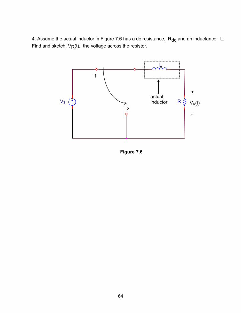
4. Assume the actual inductor in Figure 7.6 has a dc resistance, Rdc and an inductance, L.
Find and sketch, VR(t), the voltage across the resistor.
Figure 7.6
L
2
VCC
R
1
VS actual inductor
+ VR(t) -

65
Procedure:
1. Use the technique described in part 1 of the pre-lab to determine Rint for your square wave
generator, when the generator is set to 2kHz. Use values of R that give VR readings in the
range of 1/3 Voc - 2/3 Voc. Be sure to include this as a part of your total resistance in the re-
mainder of this and other labs. You should recheck the value if you vary the frequency later in
the experiment.
Figure 7.7
C
V
1
2
R
+ vC(t) -
t = 0

66
The natural response of RC, RL and RLC circuits can be demonstrated with the use of a
square wave function generator. Consider Figure 7.7. The switch is left in position 1 for a
"long time" so that the capacitor charges to V volts. When the switch is moved to position 2
(at t = 0) the capacitor discharges and we have the natural response of the RC circuit. The
circuit in Figure 7.8 provides the same result repeatedly for the ease of viewing on the oscillos-
cope as long as T/2 is long compared to the circuit time constant, RC.
Figure 7.8
2. Construct the circuit in Figure 7.8. Use R = 470Ω and C = 0.1µF. Set the function genera-
tor for a 1 volt peak-to-peak square wave of 2 KHz. Use the oscilloscope to observe, vc (t).
Sketch the portion of the waveform in which the capacitor is discharging. Use your sketch to
determine the time constant of the circuit. Compare this to the theoretical time constant (be
sure to include the internal resistance of the source).
3. Repeat part 2 for R = 6.8kΩ and C = 0.1µF. Adjust the frequency of the function generator
to obtain an adequate display.
4. Using the procedure described in part 3 of the pre-lab, find Rdc for a 68mH inductor.
+
C
R
vs(t)
-
vs(t)
t
vC(t)
T/2

67
5. Construct the circuit of Figure 7.9. Use R = 680Ω and L = 68mH. Set the amplitude of vs(t)
to a 1 volt peak-to-peak square wave. Adjust the frequency of the function generator for an
adequate display of the resistor voltage as it decreases. Sketch the voltage and determine the
time constant of your circuit from the sketch. Compare this value to the calculated time con-
stant. Be sure to include the effects of Rint and Rdc into your calculations.
Figure 7.9
6. Using the above procedure, find (experimentally) the dc resistance and the inductance of
the unknown inductor supplied by your lab instructor.
7. Use PSPICE1 (TRANSIENT ANALYSIS) to plot vc(t), t > 0, for the circuit in Figure 7.7.
Compare your output to the sketch obtained in the lab. Do this for C = 0.1µF and
R = 470Ω and 6.8kΩ ohms.
8. Use PSPICE1 to obtain the resistor voltages that you obtained in parts 5 and 6 of the proce-
dure. Compare them to your experimental results also.
1NOTE: It is not necessary to use the pulse input here. You can analyze the circuit (for t 0)
as it is shown in Figures 7.6 & 7.7.
vR(t) vs(t)
L
+
R
-
to scope

68
EXPERIMENT EIGHT
SECOND ORDER CIRCUITS
EQUIPMENT NEEDED: 1) Oscilloscope 2) Function Generator 3) Resistors, Capacitors, Inductors 4) ELVIS
THEORY
The Differential Equation - 2nd Order
The differential equations of second order circuits are obtained by application of KVL and/or
KCL and using equations (7.1), (7.2), (7.6) and (7.7) that were discussed in the Theory of Ex-
periment 7. If the application of KVL or KCL results in an integro-differential equation, the de-
rivative of both sides of the equation should be taken to convert the equation into a differential
equation.
Consider a general second order differential equation
2.82
4
2
1.80
2
2,1
2
2
a
acb
a
brrootswith
cydt
dyb
dt
yda
Assume a, b, and c are positive. Three cases are considered here.
Case I 042 acb ”Overdamped” condition.
In this case, r1 and r2 are real, distinct and negative. This results in solutions of (8.1) in the form
of decaying exponentials: trtr
eAeAy 21
21 Coefficients A1 and A2 are determined using the
initial conditions of the system or circuit.
Case II 042 acb ”Critically Damped” condition.
In this case, r1 and r2 are real, equal and negative (r= r1 = r2). This results in solutions of (8.1)
in the form of following equation: rtrt teAeAy 21 or tAAey rt
21

69
Case III 042 acb ”Underdamped” condition.
In this case, r1 and r2 are complex. This results in solutions of (8.1) in the form of the following
equation: tAtAey dd
t sincos 21 where:
4.82
4
3.82
2
a
bac
a
b
d
The term α is known as the damping factor and ωd is the damped frequency.
Consider the graph of an underdamped case shown in figure 8.1 where:
5.8cos tAetv d
t
Figure 8.1
v1
v2
v(t)
t1 t2
t
TD

70
Using figure 8.1, the following items can be determined:
7.8cos
6.8cos
22
11
2
1
tAev
tAev
d
t
d
t
Dividing (8.6) by (8.7) yields:
8.812
2
1 tte
v
v
where 9.82
12
d
DD TTtt
Substituting (8.9) into (8.8) and taking the natural logarithm of both sides results in:
11.8ln2
10.82
ln
2
1
2
1
v
v
v
v
d
d

71
Preliminary Calculations:
1. For the circuit in Figure 8.2 , write a differential equation for v(t) (in terms of R, L,
and C). If L = 68mH and C = 0.01µF, what range of values for R correspond to over-, under-,
and critically damped cases?
Figure 8.2
2. Repeat 1 for the circuit in Figure 8.3 (same L and C).
Figure 8.3
+
-
R
V C v(t)L
+
-
C
R V
L
v(t)
t = 0

72
Procedure:
1. The circuit of Figure 8.4 can be used to observe the voltage, v(t) for the circuit of Figure 8.2.
As in the previous experiment, the square wave generator is used in place of the dc source in
series with a switch.
a. Use the oscilloscope to observe and sketch v(t) (while the capacitor is charging)
for R = 6.8kΩ. Vary the frequency of the square wave so that you observe v(t) until it reaches
its steady state value.
b. Repeat a. for R = 560Ω.
c. For each case, state whether the circuit is over-, under-, or critically damped.
For the underdamped case (s) calculate the theoretical damping factor, and
the damped frequency, d. Compare these to your experimental values.
(Don't forget to include the internal resistance of the square wave generator.)
d. Using PSPICE plot v(t) versus t for each of the three circuits, compare them to
your experimental results. Recall that the circuit you are analyzing is equivalent to that shown
in Figure 8.2 (zero initial conditions). You do not need to use the pulse input for PSPICE.
Figure 8.4
+
-
R
1kHz
0.01uF
2Vp-p
square
wavev(t)
68mH

73
2. Repeat step 1 for the circuit in Figure 8.5 (used to measure v(t) for the circuit of Figure 8.3).
Figure 8.5
+
-1kHz
R
2Vp-p
square
wavev(t)
0.01uF
68mH

74
EXPERIMENT NINE
IMPEDANCE AND ADMITTANCE MEASUREMENT
EQUIPMENT NEEDED:
1) Oscilloscope 2) Function Generator 3) Resistors, Capacitors, Inductor 4) ELVIS
THEORY
A simple way of solving for steady state solution of circuits with sinusoidal input is to convert
the voltages and currents to phasor notation. The voltage v(t) and current i(t) can be converted
to phasor notation as follows:
2.9cos
1.9cos
tIti
tVtv
The ratio of the phasor voltage to the phasor current is defined as the impedance.
3.9 ZI
VZ
In general impedance is complex. The real part of impedance is known as resistance and the
imaginary part as reactance.
4.9jXRZ
Reactance for an inductance and a capacitor are given below in (9.5) and (9.6) respectively.
6.91
5.9
CX
LX
C
L

75
The ratio of the phasor current to the phasor voltage is defined as the admittance.
7.9 YV
IY
Like impedance, admittance is also complex. The real part of admittance is known as conduc-
tance and the imaginary part as susceptance.
8.9jSGY
Susceptance for an inductance and a capacitor are given below in (9.9) and (9.10) respective-
ly.
10.9
9.91
CS
LS
C
L

76
All the rules of circuit analysis that were covered for the case of pure resistive circuits apply
here. The exception is that all voltages and currents are phasors, and resistors are replaced by
the impedances.
Kirchhoff's Laws:
Kirchhoff's Voltage Law: The algebraic sum of the voltages around any closed path is zero.
11.901
N
n
nV
Kirchhoff's Current Law: The algebraic sum of the currents at any node is zero.
12.901
N
n
nI
Series Circuit:
A series circuit in terms of phasors and impedance is shown in Figure 9.1. The current I in the
series circuit is the same through all elements and other rules are similar to those of resistive
circuit.
Figure 9.1
KVL: 13.9321 NVVVVV
Total Impedance: 14.9321 NS ZZZZZ
V
Z1 Z2
Z3
ZN
+ V1 - + V2 -
+ V3 -
+ VN -

77
Voltage Divider Rule:
11.93
3
22
11
VZ
ZV
VZ
ZV
VZ
ZV
VZ
ZV
S
NN
S
S
S
Parallel Circuit:
A parallel circuit in terms of phasors and admittances is shown in Figure 9.2. The voltage V
across parallel elements is the same and other rules are similar to those of resistive circuit.
Figure 9.2
KCL : 12.9321 NIIIII
Total Admittance: 13.9321 NP YYYYY
Y1 Y V Y2
-
+
Y3 I
I1 I2
I3
IN

78
Current Divider Rule:
14.93
3
22
11
VY
YI
VY
YI
VY
YI
VY
YI
S
NN
P
P
P
Phase Measurement
In general phasor voltages and current as well as impedances are complex. Hence measur-
ing the phase becomes as important as the amplitude. The input voltage source can be con-
sidered as having zero degree phase shift and the phase of other voltages and/or currents in a
circuit are measured with respect to the input. There are actually two methods of measuring
the phase difference between two sinusoids and these methods are explained below.

79
Method 1 - Dual Trace
Consider two sinusoids having frequency = 2f. For the t axis, the difference between
peaks is , measured in radians, and this is the difference in phase between v1 and v2. (Note
that v2 lags v1.) However, on an oscilloscope, the axis is time t.
Figure 9.3
Since: 15.9
Dt
then 16.92
radiansT
tt DD
The phase angle can also be expressed in degrees:
17.93602
3602
T
t
T
t DD
tD
T
t
V
v1 v2
Tf
1

80

81
Method 2 - Lissajous Pattern
An alternative procedure for measuring phase is to apply one sinusoid to the vertical
axis y of a scope and one to the horizontal axis x. The resulting ellipse, called a Lissajous
pattern, is shown. (Figure 9.4)
Figure 9.4
18.9sin 1
A
B
A B
B
0º < φ < 90º or 270º < φ < 360º
90º < φ < 180º or 180º < φ < 270º

82
Preliminary Calculations:
1. For the circuit of Figure 9.5, calculate Z1, Z2, and Zs, the impedances of the series R-L,
the series R-C, and the entire circuit, respectively.
a. f = 1kHz C = 0.1µF
b. f = 1kHz C = 1µF
c. f = 500Hz C = 0.1 µF
2. For the three cases in part 1, calculate the phasors V1, V2, and corresponding to v1 (t),
v2 (t), and i(t), respectively).
Figure 9.5
vs(t)
1kΩ 68mH
C
680Ω
+ v2(t) -
+ v1(t) -
i(t)

83
Procedure:
1. Construct the circuit of Figure 9.5. Set the function generator for a 1V peak sinusoid with a
frequency of 1kHz. Set C = 0.1µF. Use the oscilloscope to measure the magnitude of the
phasors v1 and v2.
2. Obtain the magnitude and phase angle of the current phasor, by observing the voltage
across the 680Ω resistor.
3. Draw a phasor diagram with V1*, V2, VS, and . Include both the measured and theoreti-
cal values. Show that VS = V1 + V2 (graphically.)
4. Using the measured values of V1, V2, VS, and , calculate the impedances (mag. and
phase) Z1, Z2, and Zs (as defined in pre-lab). Show, graphically, that ZS = Z1 + Z2. Com-
pare the calculated (experimental) values to those obtained in the pre-lab.
5. Repeat 1-4 for f = 1kHz and C = 1µF.
6. Repeat 1-4 for f = 500Hz and C = 0.1µF.
*Recall that the grounds in the 2 oscilloscope inputs are common. Keep this in mind so that
you do not ground out part of your circuit.

84
EXPERIMENT 10
FREQUENCY RESPONSE
EQUIPMENT NEEDED:
1) Oscilloscope 2) Function Generator 3) Resistors, Capacitors, Inductor 4) ELVIS
THEORY
In the previous experiment, phasor voltages and currents were computed and measured for a
sinusoidal input at frequencies of 500Hz and 1kHz. Since impedances of inductors and capa-
citors are dependent on frequency of the input, the phasor voltages and currents are also fre-
quency dependent.
The frequency response considers the input-output relation in terms of amplitude and phase
for a range of desired frequencies. As an example consider a phasor series circuit shown in
Figure 10.1.
Figure 10.1
The system transfer function H(j) is defined as
1.10in
out
v
vjH
Using voltage division: 2.1021
2
21
2
ZZ
ZjHv
ZZ
Zv inout
vin vout
Z1
Z2

85
In general H(j) is complex, that is
3.10 jjHjH
The term |H (j)| is known as the amplitude response and (j) is known as the phase re-
sponse. Both |H (j)| and (j) are dependent on the input frequency
Preliminary Calculations:
1. For the circuit in Figure 10.2
a. Find an expression for H (j) = V2/V1, [V2 and V1 are the phasors for the
voltages v2(t) and v1(t) respectively].
b. Sketch | H (j)| versus , indicating the peak value and half power point.
Note: the half power point is the frequency at which |H (j) | is reduced to
1/√2 of its peak value.
c. Sketch arg H (j) versus .
Figure 10.2
v1
R
v2 C

86
2. Repeat part 1 for the circuit of Figure 10.3.
Figure 10.3
3. Repeat part 1 for the circuit of Figure 10.4.
Figure 10.4
v1 R v2
L
v1
C
R v2

87
Procedure:
1. Construct the circuit of Figure 10.2, with R = 5.1kΩ and C = 0.01µF. Set the sine wave ge-
nerator for a peak amplitude of 1 volt. Vary the frequency from 10 Hz to 100 kHz and use the
oscilloscope to measure the magnitude and phase angle (with respect to the input) of v2.
Make sure that the input remains at 1V as you vary the frequency. Use your measurements
to plot the magnitude and phase angle versus frequency. Note: Since v1 = 1V and φ1=0º,
observing v2 (j) is the same as observing H (j).
2. Determine the experimental half power point from your magnitude plot. Compare it to the
theoretical value obtained in the pre-lab.
3. Use the SPICE AC analysis to plot the magnitude and phase angle of V2 versus frequency.
Compare these to your experimental results.
4. Repeat 1-3 for the circuit of Figure 11.3 with R = 5.1kΩ and C = 0.01µF.
5. Repeat 1-3 for the circuit of Figure 11.4 with R = 3.3kΩ ohms and L = 68mH.

88
EXPERIMENT 11
PASSIVE FILTERS
EQUIPMENT NEEDED:
1) Oscilloscope 2) Function Generator 3) Resistors, Capacitors, Inductors 4) ELVIS
THEORY
Frequency response and the system transfer function H(j) were discussed in the theory of the
previous experiment. The definitions of resonant frequency r, bandwidth BW and quality fac-
tor Q are presented here for a second order RLC network. Consider the amplitude response
of a network (Figure 11.1)
Figure 11.1 – Amplitude Response
ω
H(jω)max
H(jω)max
√2
H(jω)
BW
ωc1 ωc2
ωr

89
Resonant Frequency: The frequency at which the response amplitude is maximum is known
as the resonant frequency. This frequency is denoted by r.
Cutoff Frequency: The frequency (frequencies) at which the response amplitude is
1/ √2 of maximum is (are) known as the cutoff frequency (frequencies). Figure 11.1 shows two
such frequencies denoted by ωc1 and ωc2. Sometimes these frequencies are referred to as
corner frequencies or half-power frequencies.
Bandwidth:
The width of the frequency between the cutoff frequencies ωc1 and ωc2 is known as the band-
width. That is,
1.1112 ccBW
Quality Factor:
The quality factor Q is a measure of the sharpness of peak in a resonant circuit, and is defined
as:
2.11BW
Q r
Hence smaller Q means larger bandwidth and larger Q means smaller bandwidth. In general
the amplitude response |H (j)| is not symmetrical about the resonant frequency. Normally for
a large value of Q ( >5) the amplitude response |H (j)| is symmetrical, in which case we can
write
3.112
1
BWrc
and
4.112
2
BWrc

90
Example
As an example consider the parallel RLC network shown in Figure 11.2.
Figure 11.2
Let us define the transfer function H (j) as V (j) / (j), which is the total impedance.
Hence:
5.1111
1
LCj
R
jH
The amplitude response |H (j)| is maximum if:
6.1101
L
C
VLI CR

91
The cutoff frequencies occur when
7.112
12,1 MAXcc jHjH
Therefore:
8.1111
1
2 22
LC
R
R
Solving (11.8) results in:
9.114
11
2
1221CRLCRC
c
and
10.114
11
2
1222CRLCRC
c
The bandwidth BW is evaluated by:
11.111
12RC
cc
and the quality factor Q is
12.11RCQ r
The above equations were obtained for a parallel RLC circuit. Similar procedure should be
used to obtain r, BW and Q for any other second order RLC network with sinusoidal input.
Preliminary Calculations

92
1. a. Derive an expression for H(j) = v2 (j) / v1 (j) for the circuit of Figure 11.3.
b. Sketch |H (j)| vs. .
c. What is the resonant frequency of this circuit?
d. What is the bandwidth?
e. What is the Q?
Figure 11.3
2. Repeat part 1 for the circuit of Figure 11.4.
Figure 11.4
V2 L
R1
V1 R2 C
V2
L
V1
C
R

93
Procedure:
1. a. Construct the circuit of Figure 11.3 with R = 5.1kΩ, L = 68mH,
C = 0.01µF. Set the sine wave generator for a 1V peak sinusoid. Vary the
frequency from 10Hz to 100kHz and use the oscilloscope to measure the magnitude of V2.
Make sure that the input voltage remains constant throughout the measurements. Plot the
magnitude of V2 vs. frequency on semi-log graph paper (frequency on log scale).
b. Use the above plot to find the resonant frequency of the circuit. How does it
compare to the theoretical value obtained in the pre-lab?
c. Use your graph to determine the experimental bandwidth of the circuit. How
does this value compare to the value in the pre-lab?
d. Use the AC analysis of SPICE to plot the magnitude of V2 versus frequency.
How do your results compare to those obtained in part a?
2. Repeat part 1 for R = 2kΩ ohms.
3. Repeat part 1 for the circuit of Figure 11.4 with R = 15kΩ, L = 68mH, and
C = 0.01µF.
4. Repeat part 3 for R = 5.1kΩ.
94
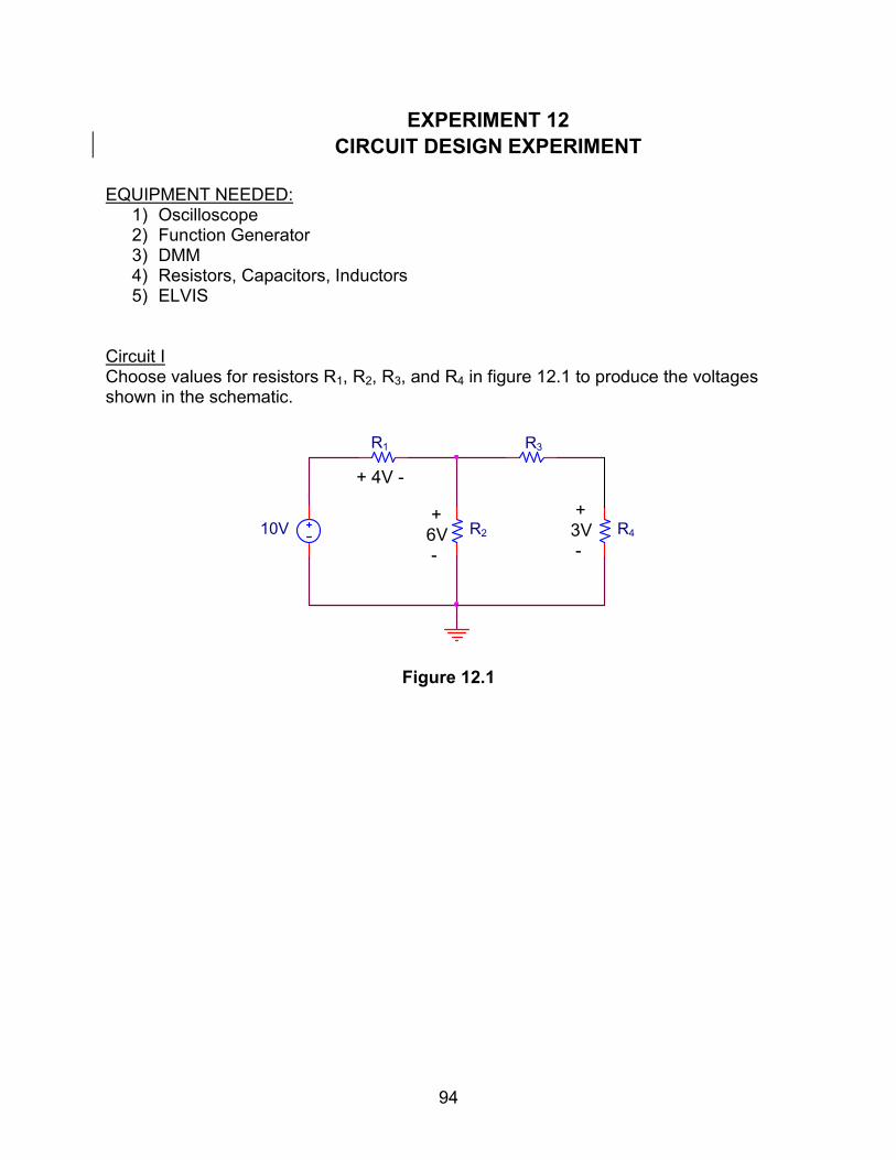
EXPERIMENT 12
CIRCUIT DESIGN EXPERIMENT
EQUIPMENT NEEDED:
1) Oscilloscope 2) Function Generator 3) DMM 4) Resistors, Capacitors, Inductors 5) ELVIS
Circuit I Choose values for resistors R1, R2, R3, and R4 in figure 12.1 to produce the voltages shown in the schematic.
Figure 12.1
R2
R1 R3
R4 10V
+ 4V -
+ 6V -
+ 3V -

95
Circuit II
For the circuit shown in figure 12.2, choose resistor values that will maximize the power dissi-
pated in the 2.7kΩ resistor.
Figure 12.2
R2
R1 R3
2.7kΩ 10

96
Circuit III
Using the circuit shown in figure 12.3, choose values for R and C that will duplicate the wave-
form shown in figure 12.4.
Figure 12.3
Figure 12.4
vc(t)
t
5V
0
2.5ms
+
C
R
vs(t)
-
vC(t)
0V – 5V square wave

97
APPENDIX
Resistor
Color Coding

98
RESISTOR VALUES
Resistors are available in certain standard values. The 5% tolerance resistors available in this
lab have values of:
A x 10b
where A = 10, 11, 12, 13, 15, 16, 18, 20, 22, 24, 27, 30, 33, 36, 39, 43, 47, 51, 56, 62,
68, 75, 82, 91, 100
and b = 1, 2, 3, 4, 5 or 6
(i.e. 2K ohms and 2.2K ohms are available, but 2.1K ohms is not). The value of a resistor is
read in the following way:
4-BAND RESISTORS
±10%
± 5% BANDS 1 2 Multiplier Tolerance
Band 1 Band 2 Multiplier Resistance
1st Digit 2nd Digit Tolerance
Color Digit Color Digit Color Multiplier Color Tolerance
Black 0 Black 0 Black 1 Silver ±10%
Brown 1 Brown 1 Brown 10 Gold ± 5%
Red 2 Red 2 Red 100 Brown ± 1%
Orange 3 Orange 3 Orange 1,000
Yellow 4 Yellow 4 Yellow 10,000
Green 5 Green 5 Green 100,000
Blue 6 Blue 6 Blue 1,000,000
Violet 7 Violet 7 Silver 0.01
Gray 8 Gray 8 Gold 0.1
White 9 White 9