c p u uniciclo
TRANSCRIPT

Organzación de CPU
Cecilia Hernández

Componentes sistema computacional
CPU
Memoria
Módulosde
Salida
Secciónde
Datos
Sw
Secciónde
Control
Módulosde
Entrada Fwy
Hw
Compilador oIntérprete
Interfaz de SwISA
Sistema Operativo
Aplicaciones

Diseño de ProcesadorSección de Datos y Control
JerarquíaMemoria
Control ALU
RegistersPC
estado
Bus Memoria
CPU
Sección de datos
Combinational
Secuencial

Diseño de CPU
Sección de datos Como fluyen los datos entre los diferentes componentes Que operaciones pueden ser realizadas cuando los datos
fluyen Que puede realizarse en un ciclo de reloj
Unidad de control Envia señales a los elementos de la sección de datos Establece direcciones de datos de origen y destino y que
operaciones se pueden realizar Jerarquía de Memoria
Mantiene el programa a ejecutar con sus datos

Organización de la CPU
ISA determina la interfaz hardware/software Desempeño determinado por
Número de instrucciones Período del reloj Ciclos de reloj por instrucción (CPI)
Diseño del procesador (datos y control) determina Período del reloj Ciclos por instrucción
Primer ejercicio: diseño de un procesador uniciclo Un ciclo por instrucción Simple de implementar, pero período es innecesariamente
grande
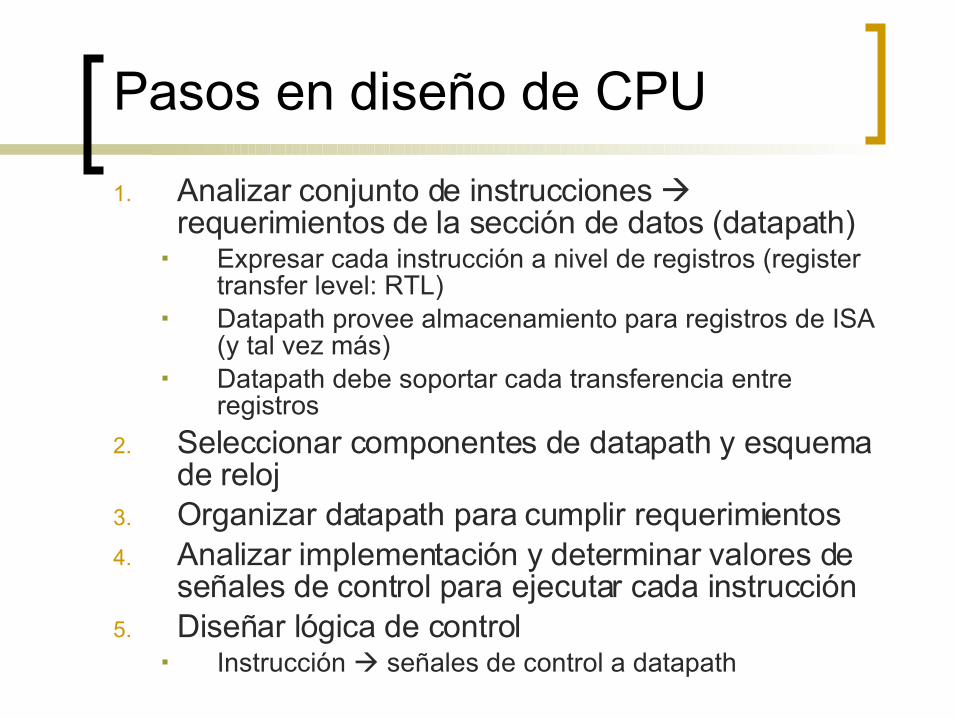
Pasos en diseño de CPU
1. Analizar conjunto de instrucciones requerimientos de la sección de datos (datapath)
Expresar cada instrucción a nivel de registros (register transfer level: RTL)
Datapath provee almacenamiento para registros de ISA (y tal vez más)
Datapath debe soportar cada transferencia entre registros
2. Seleccionar componentes de datapath y esquema de reloj
3. Organizar datapath para cumplir requerimientos4. Analizar implementación y determinar valores de
señales de control para ejecutar cada instrucción5. Diseñar lógica de control
Instrucción señales de control a datapath

Formato instrucciones MIPS
op target address
02631
6 bits 26 bits
op rs rt rd shamt funct
061116212631
6 bits 6 bits5 bits5 bits5 bits5 bits
op rs rt immediate
016212631
6 bits 16 bits5 bits5 bits
R-type
I-type
J-type

Paso 1a: Subset de MIPS
ADD and SUB add rd, rs, rt
OR Immediate: ori rt, rs, imm16
LOAD and STORE Word lw rt, rs, imm16 sw rt, rs, imm16
BRANCH: beq rs, rt, imm16
op rs rt rd shamt funct061116212631
6 bits 6 bits5 bits5 bits5 bits5 bits
op rs rt immediate016212631
6 bits 16 bits5 bits5 bits
op rs rt immediate016212631
6 bits 16 bits5 bits5 bits
op rs rt immediate016212631
6 bits 16 bits5 bits5 bits
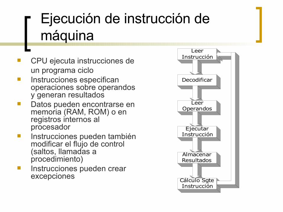
Ejecución de instrucción de máquina
CPU ejecuta instrucciones de un programa ciclo
Instrucciones especifican operaciones sobre operandos y generan resultados
Datos pueden encontrarse en memoria (RAM, ROM) o en registros internos al procesador
Instrucciones pueden también modificar el flujo de control (saltos, llamadas a procedimiento)
Instrucciones pueden crear excepciones
LeerInstrucción
Decodificar
LeerOperandos
EjecutarInstrucción
AlmacenarResultados
Cálculo SgteInstrucción
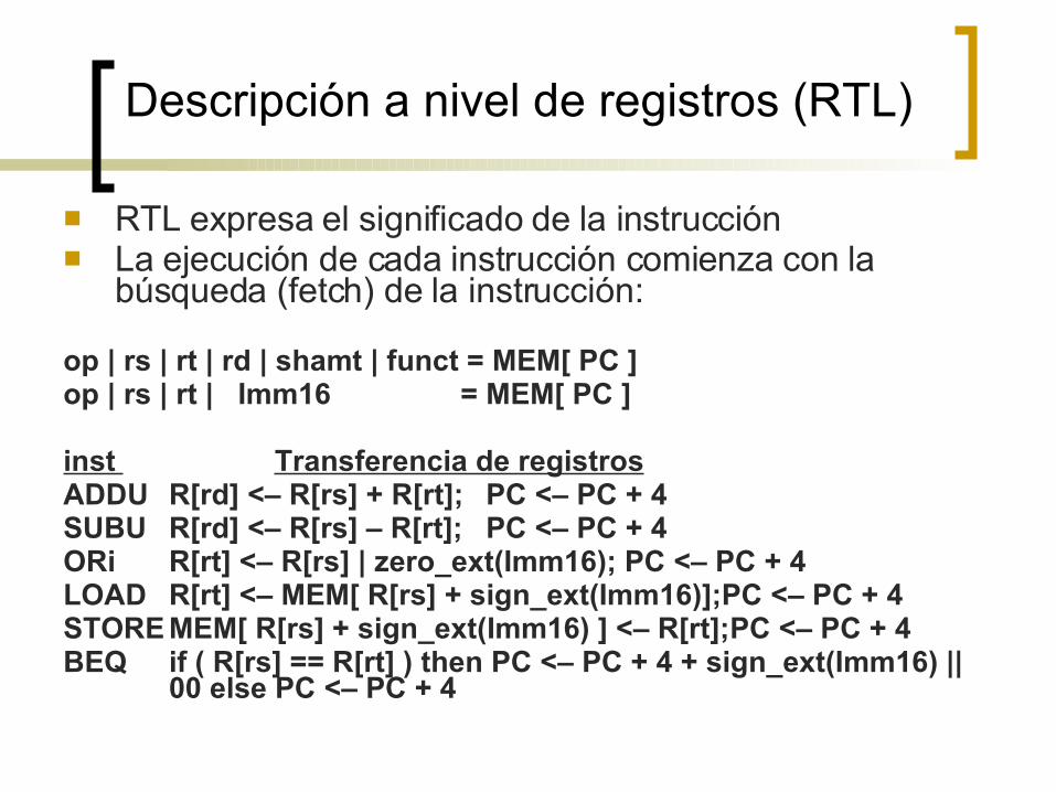
Descripción a nivel de registros (RTL)
RTL expresa el significado de la instrucción La ejecución de cada instrucción comienza con la
búsqueda (fetch) de la instrucción:
op | rs | rt | rd | shamt | funct = MEM[ PC ]op | rs | rt | Imm16 = MEM[ PC ]
inst Transferencia de registrosADDU R[rd] <– R[rs] + R[rt]; PC <– PC + 4SUBU R[rd] <– R[rs] – R[rt]; PC <– PC + 4ORi R[rt] <– R[rs] | zero_ext(Imm16); PC <– PC + 4LOAD R[rt] <– MEM[ R[rs] + sign_ext(Imm16)];PC <– PC + 4STORE MEM[ R[rs] + sign_ext(Imm16) ] <– R[rt];PC <– PC + 4BEQ if ( R[rs] == R[rt] ) then PC <– PC + 4 + sign_ext(Imm16) ||
00 else PC <– PC + 4

Paso 1: Requerimientos del conjunto de instrucciones
Memoria Instrucciones y datos
Registros (32 x 32) Leer Rs Leer Rt Escribir Rd o Rt
PC Extensor (signo o ceros) Sumar, restar y OR registros o constante
extendida Sumar 4 o constante extendida a PC

Paso 2: Componentes de la sección de datos (datapath)
Elementos combinacionales Elementos de almacenamiento
Esquema de reloj

Elementos combinacionales
Sumador (adder)
Multiplexor (MUX)
32
32
A
B32 Sum
Carry
32
32
A
B32 Result
OP
32A
B 32
Y32
SelectA
dd
erM
UX
AL
U
CarryIn
Unidad aritmético-lógica (ALU)
Bit Zero Result

Elementos de almacenamiento
Registro Similar a flip-flop tipo D,
excepto Entrada y salida de N bits Habilitación de escritura
(Write Enable)
Write Enable: Falso (0): Data Out no
cambia Verdadero (1): Data Out
cambia a Data In
Clk
Data In
Write Enable
N N
Data Out
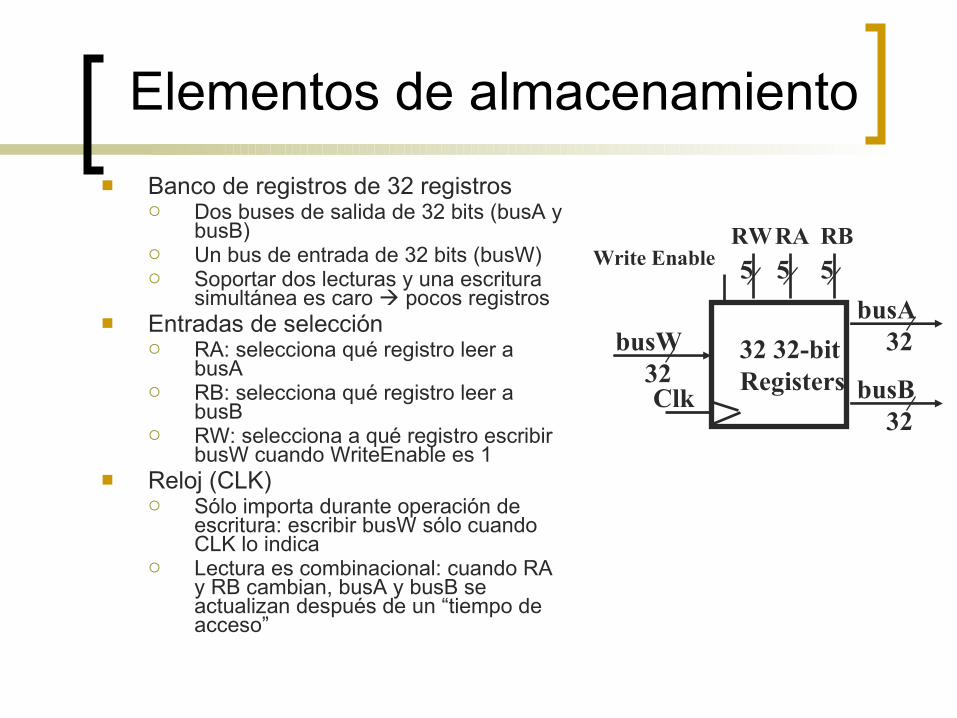
Elementos de almacenamiento
Banco de registros de 32 registros Dos buses de salida de 32 bits (busA y
busB) Un bus de entrada de 32 bits (busW) Soportar dos lecturas y una escritura
simultánea es caro pocos registros Entradas de selección
RA: selecciona qué registro leer a busA
RB: selecciona qué registro leer a busB
RW: selecciona a qué registro escribir busW cuando WriteEnable es 1
Reloj (CLK) Sólo importa durante operación de
escritura: escribir busW sólo cuando CLK lo indica
Lectura es combinacional: cuando RA y RB cambian, busA y busB se actualizan después de un “tiempo de acceso”
Clk
busW
Write Enable
3232
busA
32busB
5 5 5RWRA RB
32 32-bitRegisters

Elementos de almacenamiento
Memoria idealizada Un bus de entrada (DataIn) Un bus de salida (DataOut)
Selección de palabra en memoria Address indica la dirección de la
palabra WriteEnable = 1 Address selecciona
palabra a escribir en memoria vía DataIn
Señal de reloj (CLK) Válida sólo durante escritura
escribir cuando WriteEnable = 1 en tiempo indicado por el reloj
Para lectura, memoria es combinacional: DataIn se actualiza cuando Address cambia, después de un “tiempo de acceso”
Clk
Data In
Write Enable
32 32DataOut
Address

Esquema de reloj
Todos los elementos de almacenamiento sincronizados por el mismo canto del reloj
Clk
Don’t Care
Setup Hold
.
.
.
.
.
.
.
.
.
.
.
.
Setup Hold

Paso 3: Diseñar datapath
Cumplir requerimientos de RTL de instrucciones Búsqueda de instrucción Lectura de operandos Ejecución de operación Escritura de resultados Actualización del PC

Paso 3a: Unidad de búsqueda de instrucción RTL común a todas las instrucciones
Fetch: MEM[PC] Actualizar el contador de programa
Instrucciones secuenciales: PC PC + 4 Branch y Jump: PC destino del salto (condicional)
32
Instrucción leídaAddress
Memoria conInstrucciones
PCClk
CálculoPróx. Inst.

Unidad de búsqueda de instrucción
Si instrucción es la siguiente secuencialmente
Address
Memoria conInstrucciones
PC Sumador
32
4
Instrucción32

Unidad de búsqueda de instrucción Si siguiente instrucción determinada por branch
Address
Memoria conInstrucciones
PC
Sumador
4
Instrucción 32
Sumador
Ext Signo
Despl2 izq
Imm
MU
X
PCsel

Paso 3b: Suma y Resta
R[rd] R[rs] op R[rd] Ejemplo add rd, rs, rt Ra, Rb y Rw vienen de campos de la instrucción: rs, rt y rd ALUctr y RegWr: provienen de la unidad de control que decodifica la
instrucción ( a partir de campos op y funct de la instrucción)
32
Result
ALUctr
Clk
busW
RegWr
32
32
busA
32
busB
5 5 5
Rw Ra Rb
32 32-bitRegistros
Rs RtRd
AL
U
32
Result
ALUctr
Clk
busW
RegWr
32
32
busA
32
busB
5 5 5
Rw Ra Rb
32 32-bit
Rs RtRd
AL
U
32
Resultado
ALUctr
Clk
busW
RegWr
32
32
busA
32
busB
5 5 5
Rw Ra Rb
32 32-bitRegist
Rs RtRd
AL
Uop rs rt rd shamt funct
061116212631
6 bits 6 bits5 bits5 bits5 bits5 bits

Diagrama de tiempo
32Result
ALUctr
Clk
busW
RegWr
3232
busA
32busB
5 5 5
Rw Ra Rb
32 32-bitRegisters
Rs RtRd
AL
U
Clk
PC
Rs, Rt, Rd,Op, Func
Clk-to-Q
ALUctr
Instruction Memory Access Time
Old Value New Value
RegWr Old Value New Value
Delay through Control Logic
busA, BRegister File Access Time
Old Value New Value
busWALU Delay
Old Value New Value
Old Value New Value
New ValueOld Value
Register WriteOccurs Here

Paso 3c: Operaciones lógicas con constantes
R[rt] R[rs] op ZeroExt[imm16]Ejemplo: ori rt, rs, imm16
op rs rt immediate016212631
6 bits 16 bits5 bits5 bits
immediate16 1531
16 bits16 bits0 0 0 0 0 0 0 0 0 0 0 0 0 0 0 0
32
Result
ALUctr
Clk
busW
RegWr
32
32
busA
32
busB
5 5 5
Rw Ra Rb
32 32 -bitRegisters
Rs
ZeroE
xt
Mux
RtRdRegDst
Mux
3216imm16
ALUSrc
AL
U
Rt ?
32
Result
ALUctr
Clk
busW
RegWr
32
32
busA
32
busB
5 5 5
Rw Ra Rb
32 32 -bitRegisters
Rs
ZeroE
xt
Mux
RtRdRegDst
Mux
RtRdRegDst
Mux
3216imm16
ALUSrc
AL
U
Rt ?
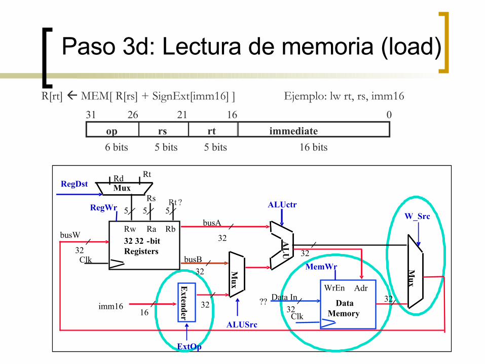
Paso 3d: Lectura de memoria (load)
R[rt] MEM[ R[rs] + SignExt[imm16] ] Ejemplo: lw rt, rs, imm16
op rs rt immediate
016212631
6 bits 16 bits5 bits5 bits
32
ALUctr
Clk
busW
RegWr
32
32
busA
32
busB
5 5 5
Rw Ra Rb32 32 -bitRegisters
Rs
RtRd
RegDst
Exten
der
Mu
x
Mux
3216
imm16
ALUSrc
ExtOp
Clk
Data InWrEn
32
Adr
DataMemory
32
AL
U
MemWr Mu
x
W_Src
??
Rt ?
32
ALUctr
Clk
busW
RegWr
32
32
busA
32
busB
5 5 5
Rw Ra Rb32 32 -bitRegisters
Rs
RtRdRegDst
Exten
der
Mu
x
Mux
3216
imm16
ALUSrc
ExtOp
Clk
Data InWrEn
32
Adr
DataMemory
32
AL
U
MemWr Mu
x
W_Src
??
Rt ?

Paso 3e: Escritura en memoria (store)
MEM[ R[rs] + SignExt[imm16] ] R[rt] Ejemplo: sw rt, rs, imm16
op rs rt immediate
016212631
6 bits 16 bits5 bits5 bits
32
ALUctr
Clk
busW
RegWr
3232
busA
32busB
55 5
Rw Ra Rb32 32 -bitRegisters
Rs
Rt
Rt
RdRegDst
Exten
der
Mu
x
Mux
3216imm16
ALUSrcExtOp
Clk
Data InWrEn
32Adr
DataMemory
MemWr
AL
U
32
Mu
x
W_Src
32
ALUctr
Clk
busW
RegWr
3232
busA
32busB
55 5
Rw Ra Rb32 32 -bitRegisters
Rs
Rt
Rt
RdRegDst
Exten
der
Mu
x
Mux
3216imm16
ALUSrcExtOp
Clk
Data InWrEn
32Adr
DataMemory
MemWr
AL
U
32
Mu
x
W_Src

Paso 3f: Salto condicional (branch)
op rs rt immediate
016212631
6 bits 16 bits5 bits5 bits
beq rs, rt, imm6
Mem[PC] Buscar instrucción de memoria
Equal R[rs] == R[rt] ? Calcular condición de salto
If (Equal) Calcular dirección de siguiente instrucciónPC PC + 4 + SignExt(imm16)
ElsePC PC + 4

Paso 3f: Salto condicional (branch)
beq rs, rt, imm16 Condición generada por datapath
op rs rt immediate
016212631
6 bits 16 bits5 bits5 bits
32
imm16P
CClk
00
Adder
Mux
Adder
4nPC_sel
Clk
busW
RegWr
32
busA
32
busB
5 5 5
Rw Ra Rb
32 32 -bitRegisters
Rs Rt
Equ
al?
Cond
PC
Ext
Inst Address
32
imm16P
CClk
00
Adder
Adder
Mux
Mux
Adder
4
Adder
Adder
4nPC_sel
Clk
busW
RegWr
32
busA
32
busB
5 5 5
Rw Ra Rb
32 32 -bitRegisters
Rs Rt
Equ
al?
Cond
PC
Ext
Inst Address
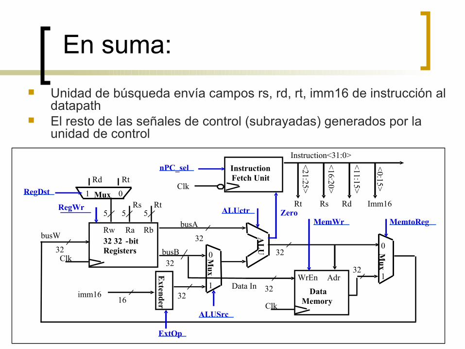
En suma:
Unidad de búsqueda envía campos rs, rd, rt, imm16 de instrucción al datapath
El resto de las señales de control (subrayadas) generados por la unidad de control
32
ALUctr
Clk
busW
RegWr
3232
busA
32busB
55 5
Rw Ra Rb32 32 -bitRegisters
Rs
Rt
Rt
Rd
RegDst
Exten
der
Mu
x
Mux
3216imm16
ALUSrc
ExtOp
Mu
x
MemtoReg
Clk
Data InWrEn
32Adr
DataMemory
32
MemWr
AL
U
InstructionFetch Unit
Clk
Zero
Instruction<31:0>
0
1
0
1
01
<21:25>
<16:20>
<11:15>
<0:15>
Imm16RdRsRt
nPC_sel
32
ALUctr
Clk
busW
RegWr
3232
busA
32busB
55 5
Rw Ra Rb32 32 -bitRegisters
Rs
Rt
Rt
Rd
RegDst
Exten
der
Mu
x
Mux
3216imm16
ALUSrc
ExtOp
Mu
x
MemtoReg
Clk
Data InWrEn
32Adr
DataMemory
32
MemWr
AL
U
InstructionFetch Unit
Clk
Zero
Instruction<31:0>
0
1
0
1
01
<21:25>
<16:20>
<11:15>
<0:15>
Imm16RdRsRt
nPC_sel

Señales de control
nPC_MUX_sel 0 PC PC + 41 PC PC + 4 + SignExt(imm16) || 00
Adr
InstMemory
Ad
der
Ad
der
PC
Clk
00
Mu
x
4
nPC_MUX_sel
PC
Extim
m16
Adr
InstMemory
Ad
der
Ad
der
Ad
der
Ad
der
PC
Clk
00
Mu
xM
ux
4
nPC_MUX_sel
PC
Extim
m16

Señales de Control
ExtOp: “zero”, “sign” MemWr: 1 Escribir en memoriaALUSrc: 0 regB; 1 constante MemToReg: 0 ALU; 1 MemALUctr: “add”, “sub”, “or” RegDst: 0 “rt”; 1 “rd”
RegWr: 1 Escribir en registro
32
ALUctr
Clk
busW
RegWr
32
32
busA
32
busB
55 5
Rw Ra Rb
32 32-bitRegisters
Rs
Rt
Rt
RdRegDst
Exten
der
Mu
x
3216imm16
ALUSrcExtOp
Mu
x
MemtoReg
Clk
Data InWrEn32 Adr
DataMemory
MemWr
AL
U
Equal
0
1
0
1
01
=
32
ALUctr
Clk
busW
RegWr
32
32
busA
32
busB
55 5
Rw Ra Rb
32 32-bitRegisters
Rs
Rt
Rt
RdRegDst
Exten
der
Mu
x
3216imm16
ALUSrcExtOp
Mu
x
MemtoReg
Clk
Data InWrEn32 Adr
DataMemory
MemWr
AL
U
Equal
0
1
0
1
01
=
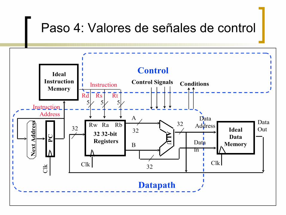
Paso 4: Valores de señales de control
DataOut
Clk
5
Rw Ra Rb
32 32-bitRegisters
Rd
AL
U
Clk
Data In
DataAddress
IdealData
Memory
Instruction
InstructionAddress
IdealInstruction
Memory
Clk
PC
5Rs
5Rt
32
323232
A
B
Nex
t A
dd
ress
Control
Datapath
Control Signals Conditions
DataOut
Clk
5
Rw Ra Rb
32 32-bitRegisters
Rd
AL
UA
LU
Clk
Data In
DataAddress
IdealData
Memory
Instruction
InstructionAddress
IdealInstruction
Memory
Clk
PC
5Rs
5Rt
32
323232
A
B
Nex
t A
dd
ress
Control
Datapath
Control Signals Conditions
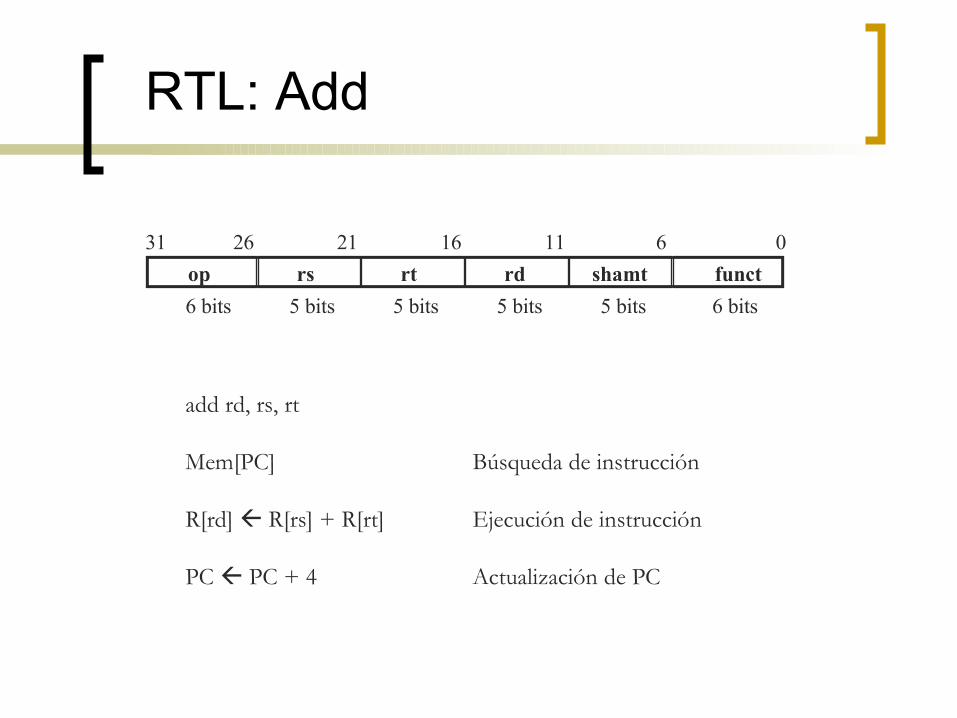
RTL: Add
op rs rt rd shamt funct
061116212631
6 bits 6 bits5 bits5 bits5 bits5 bits
add rd, rs, rt
Mem[PC] Búsqueda de instrucción
R[rd] R[rs] + R[rt] Ejecución de instrucción
PC PC + 4 Actualización de PC
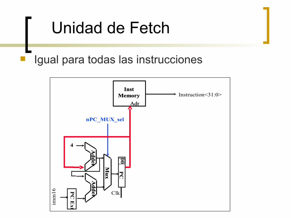
Unidad de Fetch
Igual para todas las instrucciones
PC
Ext
Adr
InstMemory
Ad
der
Ad
der
PC
Clk
00
Mu
x
4
nPC_MUX_sel
imm
16
Instruction<31:0>
PC
Ext
Adr
InstMemory
Adr
InstMemory
Ad
der
Ad
der
Ad
der
Ad
der
PC
Clk
00
Mu
xM
ux
4
nPC_MUX_sel
imm
16
Instruction<31:0>
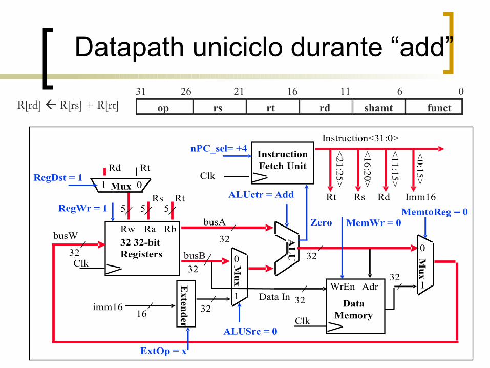
Datapath uniciclo durante “add”
op rs rt rd shamt funct
061116212631R[rd] R[rs] + R[rt]
32
ALUctr = Add
Clk
busW
RegWr = 1
32
32
busA
32
busB
55 5
Rw Ra Rb
32 32-bitRegisters
Rs
Rt
Rt
RdRegDst = 1
Exten
der
Mu
x
Mux
3216imm16
ALUSrc = 0
ExtOp = x
Mu
x
MemtoReg = 0
Clk
Data InWrEn
32
Adr
DataMemory
32
MemWr = 0
AL
U
InstructionFetch Unit
Clk
Zero
Instruction<31:0>
0
1
0
1
01
<21:25>
<16:20>
<11:15>
<0:15>
Imm16RdRsRt
nPC_sel= +4
32
ALUctr = Add
Clk
busW
RegWr = 1
32
32
busA
32
busB
55 5
Rw Ra Rb
32 32-bitRegisters
Rs
Rt
Rt
RdRegDst = 1
Exten
der
Mu
x
Mux
3216imm16
ALUSrc = 0
ExtOp = x
Mu
x
MemtoReg = 0
Clk
Data InWrEn
32
Adr
DataMemory
32
MemWr = 0
AL
U
InstructionFetch Unit
Clk
Zero
Instruction<31:0>
0
1
0
1
01
<21:25>
<16:20>
<11:15>
<0:15>
Imm16RdRsRt
nPC_sel= +4
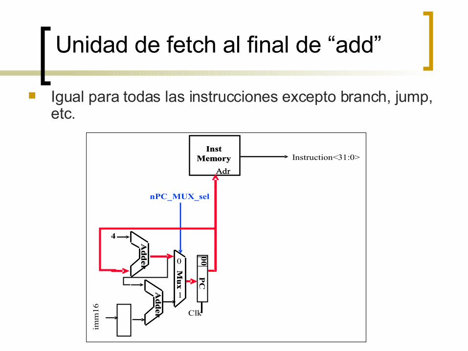
Unidad de fetch al final de “add”
Igual para todas las instrucciones excepto branch, jump, etc.
Adr
InstMemory
Ad
der
Ad
der
PC
Clk
00
Mu
x
4
nPC_MUX_sel
imm
16
Instruction<31:0>
0
1
Adr
InstMemory
Adr
InstMemory
Ad
der
Ad
der
Ad
der
Ad
der
PC
Clk
00
Mu
xM
ux
4
nPC_MUX_sel
imm
16
Instruction<31:0>
0
1

Datapath uniciclo durante “ori”
op rs rt immediate016212631
R[rt] R[rs] or ZeroExt(imm16)
Clk
32
ALUctr = Or
Clk
busW
RegWr = 1
32
32
busA
32
busB
55 5
Rw Ra Rb
32 32-bitRegisters
Rs
Rt
Rt
RdRegDst = 0
Exten
der
Mu
x
Mux
3216imm16
ALUSrc = 1
ExtOp = 0
Mu
x
MemtoReg = 0
Data InWrEn
32
Adr
DataMemory
32
MemWr = 0
AL
U
InstructionFetch Unit
Clk
Zero
Instruction<31:0>
0
1
0
1
01
<21:2
5>
<16
:20>
<11
:15>
<0
:15>
Imm16RdRsRt
nPC_sel= +4
Clk
32
ALUctr = Or
Clk
busW
RegWr = 1
32
32
busA
32
busB
55 5
Rw Ra Rb
32 32-bitRegisters
Rs
Rt
Rt
RdRegDst = 0
Exten
der
Mu
x
Mux
3216imm16
ALUSrc = 1
ExtOp = 0
Mu
x
MemtoReg = 0
Data InWrEn
32
Adr
DataMemory
32
MemWr = 0
AL
U
InstructionFetch Unit
Clk
Zero
Instruction<31:0>
0
1
0
1
01
<21:2
5>
<16
:20>
<11
:15>
<0
:15>
Imm16RdRsRt
nPC_sel= +4

Datapath uniciclo durante “lw”
op rs rt immediate016212631
R[rt] Dmem[R[rs]+SignExt(imm16)]
32
ALUctr= Add
Clk
busW
RegWr = 1
32
32
busA
32
busB
55 5
Rw Ra Rb
32 32-bitRegisters
Rs
Rt
Rt
RdRegDst = 0
Exten
der
Mu
x
Mux
3216imm16
ALUSrc = 1
ExtOp = 1
Mu
x
MemtoReg = 1
Clk
Data InWrEn
32
Adr
DataMemory
32
MemWr = 0A
LU
InstructionFetch Unit
Clk
Zero
Instruction<31:0>
0
1
0
1
01
<21:2
5>
<16
:20>
<11
:15>
<0:1
5>
Imm16RdRsRt
nPC_sel= +4
32
ALUctr= Add
Clk
busW
RegWr = 1
32
32
busA
32
busB
55 5
Rw Ra Rb
32 32-bitRegisters
Rs
Rt
Rt
RdRegDst = 0
Exten
der
Mu
x
Mux
3216imm16
ALUSrc = 1
ExtOp = 1
Mu
x
MemtoReg = 1
Clk
Data InWrEn
32
Adr
DataMemory
32
MemWr = 0A
LU
InstructionFetch Unit
Clk
Zero
Instruction<31:0>
0
1
0
1
01
<21:2
5>
<16
:20>
<11
:15>
<0:1
5>
Imm16RdRsRt
nPC_sel= +4

Datapath uniciclo durante “sw”
op rs rt immediate
016212631Dmem[R[rs]+SignExt(imm16)] R[rt]
32
ALUctr= Add
Clk
busW
RegWr = 0
32
32
busA
32
busB
55 5
Rw Ra Rb
32 32-bitRegisters
Rs
Rt
Rt
RdRegDst = x
Exten
der
Mu
x
Mux
3216imm16
ALUSrc = 1
ExtOp = 1
Mu
x
MemtoReg = x
Clk
Data InWrEn
32Adr
DataMemory
32
MemWr = 1
AL
U
InstructionFetch Unit
Clk
Zero
Instruction<31:0>
0
1
0
1
01
<21:25>
<16:20>
<11:15>
<0:15>
Imm16RdRsRt
nPC_sel= +4
32
ALUctr= Add
Clk
busW
RegWr = 0
32
32
busA
32
busB
55 5
Rw Ra Rb
32 32-bitRegisters
Rs
Rt
Rt
RdRegDst = x
Exten
der
Mu
x
Mux
3216imm16
ALUSrc = 1
ExtOp = 1
Mu
x
MemtoReg = x
Clk
Data InWrEn
32Adr
DataMemory
32
MemWr = 1
AL
U
InstructionFetch Unit
Clk
Zero
Instruction<31:0>
0
1
0
1
01
<21:25>
<16:20>
<11:15>
<0:15>
Imm16RdRsRt
nPC_sel= +4

Datapath uniciclo durante “ beq”
op rs rt immediate016212631
If (R[rs] – R[rt] == 0) then Zero 1Else Zero 0
Clk
32
ALUctr =Sub
Clk
busW
RegWr = 0
32
32
busA
32busB
55 5
Rw Ra Rb32 32-bitRegisters
Rs
Rt
Rt
RdRegDst = x
Exten
der
Mu
x
Mux
3216imm16
ALUSrc = 0
ExtOp = x
Mu
x
MemtoReg = x
Data InWrEn
32Adr
DataMemory
32
MemWr = 0A
LU
InstructionFetch Unit
Clk
Zero
Instruction<31:0>
0
1
0
1
01
<21
:25>
<16
:20>
<11:1
5>
<0
:15
>
Imm16RdRsRt
nPC_sel= “Br”
Clk
32
ALUctr =Sub
Clk
busW
RegWr = 0
32
32
busA
32busB
55 5
Rw Ra Rb32 32-bitRegisters
Rs
Rt
Rt
RdRegDst = x
Exten
der
Mu
x
Mux
3216imm16
ALUSrc = 0
ExtOp = x
Mu
x
MemtoReg = x
Data InWrEn
32Adr
DataMemory
32
MemWr = 0A
LU
InstructionFetch Unit
Clk
Zero
Instruction<31:0>
0
1
0
1
01
<21
:25>
<16
:20>
<11:1
5>
<0
:15
>
Imm16RdRsRt
nPC_sel= “Br”

Unidad de fetch al final de “beq”
op rs rt immediate016212631If (Zero == 1) then
PC PC + 4 + SignExt[imm16]*4Else PC PC + 4
nP C_s el z ero? M UX0 x 01 0 01 1 1
Adr
InstMemory
Ad
der
Ad
der
PC
Clk
00
Mu
x
4
nPC_sel
imm
16
Instruction<31:0>
0
1
Zero
nPC_MUX_sel
nP C_s el z ero? M UX0 x 01 0 01 1 1
Adr
InstMemory
Adr
InstMemory
Ad
der
Ad
der
Ad
der
Ad
der
PC
Clk
00
Mu
xM
ux
4
nPC_sel
imm
16
Instruction<31:0>
0
1
Zero
nPC_MUX_sel

Resumen de señales de control
Proceso de decodificación de instrucciones consiste en generar estas señales
inst Register Transfer
ADD R[rd] < – R[rs ] + R[rt ]; PC < – PC + 4
ALUsrc = RegB , ALUctr = “add ”, RegDst = rd, RegWr , nPC_sel = “+4 ”
SUB R[rd] < – R[rs ] – R[rt ]; PC < – PC + 4
ALUsrc = RegB , ALUctr = “sub ”, RegDst = rd, RegWr , nPC_sel = “+4 ”
ORi R[rt ] < – R[rs ] + zero_ext(Imm16); PC < – PC + 4
ALUsrc = Im , Extop = “Z”, ALUctr = “or ”, RegDst = rt , RegWr , nPC_sel = “+4”
LOAD R[rt ] < – MEM[ R[rs ] + sign_ext(Imm16)]; PC < – PC + 4
ALUsrc = Im , Extop = “Sn ”, ALUctr = “add ”, MemtoReg , RegDst = rt , RegWr , nPC_sel = “+4 ”
STORE MEM[ R[rs ] + sign_ext(Imm16)] < – R[rs ]; PC < – PC + 4
ALUsrc = Im , Extop = “Sn ”, ALUctr = “add ”, MemWr , nPC_sel = “+4 ”
BEQ if ( R[rs ] == R[rt ] ) then PC < – PC + sign_ext(Imm16)] || 00 else PC < – PC + 4
nPC_sel = “Br ”, ALUctr = “sub ”
Instrucción Transferencia de registros
ADD R[rd] <– R[rs ] + R[rt ]; PC < – PC + 4
ALUsrc = RegB , ALUctr = “add ”, RegDst = rd, RegWr , nPC_sel = “+4 ”
SUB R[rd] < – R[rs ] – R[rt ]; PC < – PC + 4
ALUsrc = RegB , ALUctr = “sub ”, RegDst = rd, RegWr , nPC_sel = “+4 ”
ORi R[rt ] < – R[rs ] + zero_ext(Imm16); PC < – PC + 4
ALUsrc = Im , Extop = “Z”, ALUctr = “or ”, RegDst = rt , RegWr , nPC_sel = “+4”
LOAD R[rt ] < – MEM[ R[rs ] + sign_ext(Imm16)]; PC < – PC + 4
ALUsrc = Im , Extop = “Sn ”, ALUctr = “add ”, MemtoReg , RegDst = rt , RegWr , nPC_sel = “+4 ”
STORE MEM[ R[rs ] + sign_ext(Imm16)] < – R[rs ]; PC < – PC + 4
ALUsrc = Im , Extop = “Sn ”, ALUctr = “add ”, MemWr , nPC_sel = “+4 ”
BEQ if ( R[rs ] == R[rt ] ) then PC < – PC + 4 + sign_ext(Imm16)] || 00 else PC < – PC + 4
nPC_sel = “Br ”, ALUctr = “sub ”

Paso 5: Diseñar lógica de control
ALUctrRegDst ALUSrcExtOp MemtoRegMemWr Equal
Instrucción<31:0>
<21:25>
<16:20>
<11:15>
<0:15>
Imm16RdRsRt
nPC_sel
Adr
MemoriaInstruccion
SECCIÓN DE DATOS
Decoder
Op
<21:25>
Fun
RegWr
Resumen de señales de control
add sub ori lw sw beq
RegDst
ALUSrc
MemtoReg
RegWrite
MemWrite
nPCsel
ExtOp
ALUctr<2:0>
1
0
0
1
0
0
x
Add
1
0
0
1
0
0
x
Subtract
0
1
0
1
0
0
0
Or
0
1
1
1
0
0
1
Add
x
1
x
0
1
0
1
Add
x
0
x
0
0
1
x
Subtract
op target address
op rs rt rd shamt funct
061116212631
op rs rt immediate
R-type
I-type
J-type
add, sub
ori, lw, sw, beq
jump
func
op 00 0000 00 0000 00 1101 10 0011 10 1011 00 0100Appendix A10 0000Ver 10 0010 No interesa

Decodificación localUnidad de control decodifica parte de la instrucción y ALU hace su propia decodificación local
R-type ori lw sw beqRegDstALUSrcMemtoRegRegWriteMemWriteBranchExtOpALUop<N:0>
100100x
“R-type”
0101000
Or
0111001
Add
x1x0101
Add
x0x001x
Subtract
op 00 0000 00 1101 10 0011 10 1011 00 0100
MainControl
op
6
ALUControl(Local)
func
N
6ALUop
ALUctr
3
AL
U
MainControl
op
6
ALUControl(Local)
ALUControl(Local)
func
N
6ALUop
ALUctr
3
AL
U

Codificación para ALUop
MainControl
op
6
ALUControl(Local)
func
N
6ALUop
ALUctr
3A
LU
MainControl
op
6
ALUControl(Local)
ALUControl(Local)
func
N
6ALUop
ALUctr
3A
LU
ALUop: Instrucciones tipo ‘R’; instrucciones tipo ‘I’ (or, add, subtract) 2 bits
R-type ori lw sw beq
ALUop (Symbolic) “R-type” Or Add Add Subtract
ALUop<2:0> 1 00 0 10 0 00 0 00 0 01

Decodificación de campo ‘func’
op rs rt rd shamt funct061116212631
R-type
R-type ori lw sw beqALUop (Symbolic) “R-type” Or Add Add Subtract
ALUop<2:0> 1 00 0 10 0 00 0 00 0 01
funct<5:0> Instruction Operation10 000010 001010 010010 010110 1010
addsubtractandorset-on-less-than
ALUctr<2:0> ALU Operation000001010110111
AndOr
AddSubtract
Set-on-less-than
ALUctr
AL
U
MainControl
op
6
ALUControl(Local)
func
N
6ALUop
ALUctr
3A
LU
MainControl
op
6
ALUControl(Local)
ALUControl(Local)
func
N
6ALUop
ALUctr
3A
LU
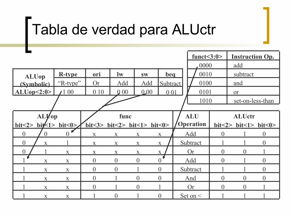
Tabla de verdad para ALUctr
R-type ori lw sw beqALUop(Symbolic) “R-type” Or Add Add Subtract
ALUop<2:0> 1 00 0 10 0 00 0 00 0 01
ALUop funcbit<2> bit<1> bit<0> bit<2> bit<1> bit<0>bit<3>
0 0 0 x x x x
ALUctrALUOperation
Add 0 1 0bit<2> bit<1> bit<0>
0 x 1 x x x x Subtract 1 1 00 1 x x x x x Or 0 0 11 x x 0 0 0 0 Add 0 1 01 x x 0 0 1 0 Subtract 1 1 01 x x 0 1 0 0 And 0 0 01 x x 0 1 0 1 Or 0 0 11 x x 1 0 1 0 Set on < 1 1 1
funct<3:0> Instruction Op.00000010010001011010
addsubtractandorset-on-less-than

Desventajas de procesador uniclo
CPI =1 pero, ¿Qué tan rápido es el reloj? Tan rápido como la instrucción más lenta Memorias reales son mucho más lentas que el procesador Instrucciones de punto flotante toman mucho más tiempo
Cada unidad funcional está ocupada por toda la instrucción Necesitamos memoria separada de programa y de datos No podemos compartir ALU para calcular siguiente PC
PC Inst Memory mux ALU Data Mem mux
PC Reg FileInst Memory mux ALU mux
PC Inst Memory mux ALU Data Mem
PC Inst Memory cmp mux
Reg File
Reg File
Reg File
Arithmetic & Logical
Load
Store
Branch
Critical Path
setup
setupPC Inst Memory mux ALU Data Mem mux
PC Reg FileInst Memory mux ALU mux
PC Inst Memory mux ALU Data Mem
PC Inst Memory cmp mux
Reg File
Reg File
Reg File
Arithmetic & Logical
Load
Store
Branch
Camino Crítico
setup
setup

Peor caso: instrucción load
Critical Path (Load Operation) = PC’s Clk-to-Q +Instruction Memory’s Access Time +Register File’s Access Time +ALU to Perform a 32-bit Add +Data Memory Access Time +Setup Time for Register File Write +Clock Skew
Clk
5
Rw Ra Rb
32 32-bitRegisters
Rd
AL
U
Clk
Data In
DataAddress
IdealData
Memory
Instruction
InstructionAddress
IdealInstruction
Memory
Clk
PC
5Rs
5Rt
16Imm
32
323232
A
B
Nex
t A
dd
ress
Camino Crítico (Instrucción Load) = Tiempo acceso PC +Tiempo de acceso a la memoria +Tiempo de acceso a Banco Reg +’ALU para realizar suma de 32 bits+-Tiempo acceso memoria de datos +Tiempo de seteo escritura en BReg +Clock Skew
Clk
5
Rw Ra Rb
32 32-bitRegistros
Rd
AL
UA
LU
Clk
Data In
Dir.Data
IdealMemoriaDatos
Instrucción
DirecciónInstrucción
IdealMemoriaInstrucción
Clk
PC
5Rs
5Rt
16Imm
32
323232
A
B
Pró
x. D
ir.

Ejemplo
Asumir que los tiempos de operación de las unidades funcionales son: Memoria: 2ns ALU y sumadores: 2ns Banco de registros: 1ns
Los retardos de multiplexores, unidad de extensión de signo, registros individuales y alambres son despreciables. Comparar el desempeño de las siguientes implementaciones:1. Máquina uniciclo de período de reloj fijo.2. Máquina uniciclo ficticia donde el período de reloj varía para
ajustarse al tiempo exacto de ejecución de cada instrucción.
Asumir que la frecuencia dinámica de ejecución de instrucciones es: 24% loads, 12% stores, 44% instrucciones ALU, 18% saltos condicionales (branches) y 2% saltos absolutos (jumps).

Solución
Banco registros
FetchJump
MemoriaALUBanco
registrosFetchStore
ALUBanco
registrosFetchBranch
MemoriaALUBanco
registrosFetchLoad
Banco registros
ALUBanco
registrosFetchALU
Uso de unidades funcionalesTipo de
instrucción

Solución
2
2
Memoria datos
2
2
2
2
ALU
1
1
1
1
Lectura banco
registros
2
2
2
2
2
Memoria de
instrucción
Jump
Branch
Store
Load
ALU
Tipo de instrucción
2ns
7ns
8ns
6ns
Total
1
1
Escritura banco registros
Período de reloj ciclo fijo: 8nsPeríodo de reloj ciclo variable: 6*0.44 + 8*0.24 + 7*0.12 + 5*0.18 + 2*0.02 = 6.3nsAceleración = 1.27

Ejemplo
Suponer una unidad de punto flotante que suma o resta en 8ns y multiplica o divide en 16ns. Todas las otras unidades funcionales tienen los retardos del ejemplo anterior. ¿Qué tanto más rápida es la implementación de reloj de período variable versus la de reloj de período fijo? Asumir que las frecuencias de ejecución son: 31% loads, 21% stores, ALU 27%, saltos condicionales 5%, saltos absolutos 2%, suma/resta de punto flotante 7%, y multiplicación/división de punto flotante 7%.
Tiempo de ejecución suma/resta de punto flotante = 2 + 1 + 8 + 1 = 12nsTiempo de ejecución multiplicación/división de punto flotante = 2 + 1 + 16 + 1 = 20ns
Ciclo de reloj período fijo = 20nsCiclo de reloj promedio período variable = 8*0.31 + 7*0.21 + 6*0.27 + 5*0.05 + 2*0.02+ 12*0.07 + 20*0.07 = 8.1ns
Aceleración = 20/8.1 = 2.47

Mejorando el desempeño
Idea: procesador multiciclo Ejecutar sólo parte de una instrucción en
cada período de reloj Reloj es más rápido Instrucciones más sencillas toman menos
ciclos en ejecutar que instrucciones más complejas