c. lindsey, chak chie, - search read.pudn.comread.pudn.com/downloads154/doc/683140/a survey of...
TRANSCRIPT

410 PROCEEDINGS OF THE IEEE, VOL. 69, NO. 4, APRIL 1981
A Survey of Digital Phase-Locked loops WILLIAM C. LINDSEY, FELMW, IEEE, AND CHAK MING CHIE, MEMBER, IEEE
Invited Paper
Absmcr-The purpose of this paper is to present a systematic suney of the theoretical/experimental work accomplished in the area of digital p h d o c k e d loops (DPLL’s) during the period of 1960 to 1980. The DPLL represenb the heart of the M a g blocks required m the implementation of coherent (In digital) communications and tracking receivers
his survey is partic- motivated by the fact that microprocessor technology is advaocing rapidly to the extent that sophisticated and flexible signal processing algorithms for communications and contrd can be realized m the digital domain. In fact, it is anticipated that the use of this signal processing tedmdogy will continue to expand rapidly in the development of advanced communications and tracking receives, e.&, aIl digital modems. Consequently, one major purpose of this paper is to provide the reader with a survey and an overview of the theoretiat and experimental work accomplished to date, thereby offering speedy acce58 to the techniques and hardware developments which have been presented ia a scattered literature. In addition, the authors feel that a tutorial artide revealing the various theories, their relatiomhips to one another, their shortcomings, their advantags and the assumptions on which each is based, would be of tremendous value to the engineer trying to decide what particular analysis p m cedure is applicable to his peculiar problem. Consequently, a byprod- uct of this presentation will be to point out unsolved problems of ~ractical interest. A broad class of digital modulation techniques, viz 1-Q modulations and demdldation, are studied in a rather g e n d way.
I. BACKGROUND
HE CONTINUED progress in increasing performince, speed, reliability, and the simultaneous reduction in size and cost of integrated circuits (LSI and VLSI) has
resulted in strong interest in the implementation of the phase locked loop (PLL) in the digital domain. A survey on analog PLL’s in 1975 by Gupta [ 11 included over 40 publications in this direction. Aside from the obvious advantages associated with digital systems, a digital version of the PLL (DPLL) alleviates some of the problems associated with its analog counterpart; namely, sensitivity to dc drifts and component saturations, difficulties encountered in building higher order loops, and the need for initial calibration and periodic adjust- ments. In addition, with the ability to perform elaborate real-time processing on the signal samples, the DPLL‘s can be made more flexible and versatile.
In contrast to the matured status of the study of the analog PLL (APLL) (e.g., see Lindsey [2], Gardner [3]; and Lindsey and Simon [ 58]), the development of the ‘all DPLL has just started to take shape over the last ten years. Like most aspects
I r
work was supported in part by the National Science Foundation under Manuscript received May 19, 1980; revised December 17,1980. This
Grant ENG782219 and by LinCom Corporation I R and D Funds. W. C. Lindsey is with the Department of Electrical Enginering, Uni-
versity of Southern California, Powell Hall, Room 524, L a Andes, CA 90007.
dena, CA 91105. C. M. Chie is with the LinCom Corporation, P.O. Box 2793D, F’asa-
SIGNAL INPUT
DETECTOR FILTER
OUTPUT I vco
VOLTACE
OSCILLATOR CONTROLLED
Fig. 1 . Block diagram of an analog PLL.
of engineering, the work on DPLL’s is motivated by the steady availability of components that offer advantages over the con- ventional ones. The classical APLL consists of three major functional units: 1) a phase detector (PD), 2) a loop filter and 3) a voltage-controlled oscillator (VCO). A block diagram of the APLL is shown in Fig. 1 . l The incoming signal whose phase is to be tracked is mixed with a locally generated sine wave to produce a voltage proportional to their instantaneous phase difference. This error voltage is filtered and used to control the instantaneous frequency of the VCO. All three components are realized with analog circuitry, e.g., the PD is a balanced mixer, the loop filter is a simple RC low-pass circuit, and the VCO is tuned by adjusting the bias voltage on a varicap in the tuned circuit controlling the resonant fre- quency of the VCO. The earliest efforts on DPLL’s concen- trated on partially replacing the APLL components with digital ones. Apparently, Westlake [4] was the f i t to docu- ment the work in this direction in 1960. He introduced a sample and hold circuit at the output of the loop filter in order to take advantage of the improvements offered by a digital VCO. In 1962, Byrne [ 51 analyzed the performance of a PLL when the phase detector was implemented with a flip- flop and hence exhibited a sawtooth PD characteristic. As another example along the same line, Gupta [6] in 1968 analyzed the effect of replacing the loop fiiter with a digital one.
Towards the end of the 19603, researchers in the field turned their attention to the implementation and design of digital PLL‘s. Perhaps the first “all digital loop” was reported by Drogin [7] in 1967. The second-order loop built and tested was used as a VHF omnidirectional range fiider. It was designed to track a relatively slow 30-Hz sine wave. All digital components were clocked synchronously by a com- mon 1.097 MHz reference. Since then, the DPLL field has
cuits, e.g., lock detection and automatic gain contrd [Z]. ‘In practice, thii circuit is usually augmented by other contrd cir-
0018-9219/81/04004410$00.75 0 1981 IEEE
Authorized licensed use limited to: GUILIN UNIVERSITY OF ELECTRONIC TECHNOLOGY. Downloaded on March 4, 2009 at 23:34 from IEEE Xplore. Restrictions apply.

LINDSEY AND CHIE: DIGITAL PHASE-LOCKED LOOPS 411
been somewhat active; the most noticeable years being 1968- 1972. Different authors explored various avenues and aspects of implementing the DPLL concept. We have found it con- venient to categorize the different implementations into four classes based on the mechanization of the phase detector.
They are: 1) Flip-Flop IFF) -DPLL in which the phase error is derived from the duration between the set and reset time of a flip-flop triggered by positive zero crossings of the input signal and the local clock; 2) Nyquist Rate (NR)-DPLL in which the input signal is sampled at the Nyquist rate; 3) Zero Crossing (2C)-DPLL in which the loop tries to sample at the zero crossings of the incoming signal; and 4) LeadlLag (LL)- DPLL in which the PD determines at each cycle whether the input leads or lags the locally generated clock. Notice that in I ) , 3), and 4) the phase of the incoming signal is measured against the reconstructed signal. However, in the case of 2), the phase of the signal is measured against a f i e d reference. For this reason, 2) is often referred to as a uniform sampling scheme whereas l), 3) and 4) are nonuniform sampling schemes.
The work by Drogin falls within the first category. Paster- nack and Whalin [ 81 then considered in 1968 a general Nth- order loop where the function of the loop fiter and the digital VCO is combined into a single unit. The loop that they pro- posed was later applied by Goto [ 91 in 1970 for synchronizing digital networks. More recently, Yamashita et al. [ 101 con- sidered a modification of the Pasternack and Whalin loop and achieved improved jitter performance.
The NR-DPLL was f i t proposed in 1968 by Larimore [ 1 1 ] and later verified by simulation in 1969 [ 121. The tracking function was implemented by a digital processor. Subse- quently, Greco et al. [ 131, [ 141 reported experimental results on a first-order NR-DPLL in 1972. Greco and Schilling [ 151 and Garodnick et al. [ 161 extended their previous work to include f i t , second and third-order loops in 1973 and 1974, respectively. A recent paper by Cahn and Leimer 1591 re- ported a scheme by which the phase of the incoming signal is sampled at the Nyquist rate and they provided experimental results.
There are two variations of the ZC-DPLL. The f i t version which we shall call ZC1-DPLL, samples only on the positive going zero crossings. This scheme was first proposed by Natali [ 171 in 1968. He considered a second-order ZCl-DPLL and provided simulation results. Later in 1972, Gill and Gupta [ 181, [ 191 systematically analyzed the first and higher order ZC1-DPLL in the absence of noise. In the same year, Natali [201 presented an experimental all digital receiver in which a Costas type ZC1-DPLL was employed for suppressed camer tracking. Reddy and Gupta [ 211 considered a fi t-order ZCl-DPLL for FM demodulation. In [221, they considered the effect of quantizing the PD output for a first-order loop. Later on, they analyzed [23] the statistical behavior of this loop (with binary quantization and a sequential filter), using the Markov chain theory. The f i t systematic statistical analysis on ZCl-DPLL was provided by Weinberg and Liu [24] in 1974 based on an approximate numerical solution to the Chapman-Kolmogorov equation. Korizumi and Mi- yakama [25] later on included the effect of sample delay in the analysis as well as presented some experimental results. Chie [26] extended the work of Weinberg and Liu by solving the Chapman-Kolmogorov equation for a Tit-order ZC1- DPLL and comparing with analog results. Recently, Lindsey and Chie [ 271, D’Andrea and Russo [281, and Russo [ 291
analyzed the acquisition behavior of the ZC1-DPLL. D’Andrea and Russo [601 considered the quantization effect of the sampler/PD on the stochastic operation of a fit-order loop. Rocha (301 demonstrated an implementation of a second- order ZCI-DPLL with time varying loop filter parameters. Chie [ 611 modified the second-order ZC1-DPLL to allow for Doppler rate tracking. Osborne [62], [63] provided the stability analysis of the Nth power ZC1-DPLL for suppressed carrier tracking.
The second type of ZC-DPLL, proposed by Holmes [31], samples on both positive and negative going zero crossings. We shall call this type of loop ZC2-DPLL. To provide the proper sign of the error voltage, the samples must be flipped in sign to distinguish between positive and negative going zero cross- ings. Holmes [ 3 1 ] f i t considered a fit-order loop. Statisti- cal analysis was based on the Markov chain theory. Later on, Tegnelia [ 321, and Holmes and Tegnelia [33] considered a second-order ZC2-DPLL. The statistical analysis was based on an equivalent APLL model. Lesh [34] suggested an effi- cient computation algorithm to determine its acquisition b e havior. Recently, Majumdar [64] and Cernuschi-Frias and Rocha [65] rediscovered the ZC2-DPLL in an attempt to in- crease the dc loop gain of the ZC1-DPLL.
The class of LL-DPLL was proposed and analyzed by Cessna and Levy [ 351, and Cessna [36] in 1972. The PD output is binary quantized and drives a sequential filter. Statistical analysis was accomplished by Markov chain theory. Their work was extended by Yamamoto and Mori [37] recently to include a “second-order” sequential filter with memory.
The work on DPLL also motivated research on developing discrete FM demodulator structures that are derived from stochastic estimation techniques. The optimum structure of the DPLL can be obtained by considering optimum digital angle demodulation using nonlinear estimation theory. This approach is an extension of Snyder’s 1661 state-variable com- munication model to include a discrete-time observation sequence that can be treated with Jazwinski’s [67] approach to continuous-discrete estimation. Approximate solutions when applied to the communication model lead to realizable DPLL structures. This work has been carried out by Kelly and Gupta [ 381, [ 391 and Polk and Gupta [ 401, [ 41 ] for the addi- tive noise case. McBride [42] considered the same problem for complex signals and arrived at receiver structures that used I-Q sampling. Subsequent works that appeared are by Hurst and Gupta [43], [44] and Weinberg and Liu [45]. The DPLL type of structures for Rayleigh and Rician fading channels have been obtained by Dharamsi and Gupta [68] and Takhar [69]. For a synopsis of available results based on the non- linear filtering theory, the interested reader is referred to the survey by Gupta [ 1 1.
In this paper, we begin by motivating the DPLL structure from a simple MAP estimation point of view. The four differ- ent implementation approaches that were categorized earlier are described in sufficient detail to understand their principle of operation. Before doing so, we shall examine the individual loop component building blocks. We then summarize the simple yet important linear analysis of DPLL based on the z-transform theory and discuss the relationqhip between APLL and DPLL parameters. Next, the theory of ZCl-DPLL is treated. We feel this particular configuration is the simplest to implement, the easiest to model and its operation and perfor- mance are indicative of the general behavior of any DPLL. We shall then consider the effect of quantization on DPLL per-
Authorized licensed use limited to: GUILIN UNIVERSITY OF ELECTRONIC TECHNOLOGY. Downloaded on March 4, 2009 at 23:34 from IEEE Xplore. Restrictions apply.

412 PROCEEDINGS OF THE IEEE, VOL. 69, NO. 4, APRIL 1981
formance and discuss the methodology of noise analysis based on Markov chain models. Finally, we shall present some recent work on suppressed carrier tracking loop configurations [461.
II. THE DPLL AND ITS RELATIONSHIP TO F’HASE ESTIMATION
The DPLL structure is most easily motivated when one con- siders the problem of maximum a posteriori (MAP) estimation of a carrier with an unknown phase. Consider N discrete ob- servables
Y k = S k + n k , 1 < k < N (2-1 1 where {sk} is a sequence of signal samples corrupted by the noise sequence { n k } . The case of interest is
sk = @sin (work + e ) (2-2)
and represents the values of a sinusoidal signal observed at the increasing time epochs { t k } . ~n (2-2), wo is the known carrier frequency, P is the carrier power and 0 is the unknown phase to be estimated. In order to proceed, we shall assume the noise samples are independent and identically distributed zero- mean Gaussian random variables. Using Bayes’ rule, the a posteriori probability density function (PDF) of the un- known phase 0 conditioned on the vector of observables Y = (A , * - - , YN) is given by
In MAP estimation, one seeks to find a 8 so that the PDF p(e1y) is maximized givenAthe observablesy. Using (2-3), this is equivalent to finding a 0 to maximize p ( y le) p ( 0 ) . TO, pro- ceed, we shall assume that p ( @ = 1/2n, 101 < R . Then, 0 also maximizes p ( y l 0 ) . By our assumption, p ( y le) is Gaussianly distributed. Therefore, using the monotoneAproperty of the exponential function, it can be shown that 0 maximizes the quadratic form
N A(e) = - 4 i y k - ,/G sin (Wotk + e)]? (2-4)
k = 1
Because p ( y l 0 ) is a unimodal function, we know that 8 is the unique solution of
a (2-5)
To continue, let
. COS (Work + e). (24 )
Equation (26 ) can be sohed by the technique of simple itera- tion. In essence, given an arbitrary starting phase estimate and provided some regularity conditions are satisfied, the equation
81+1 = 81 + A1(8l) (2-7)
defines a2equence of 81 which converges to the MAP phase estimate 5. Equations (2-6) and (2-7) can be represented by the closed loop block diagram of Fig. 2(a). The fEncticn of the digitally controlled oscillator (DCO) is to step to
N
k=O
I DIGITALLY izp s in (Uotk+ i ik ) CONTROLLED
,OSCILLATOR
CONTROLLED DIGITALLY
OSCILLATOR
(b) Fig. 2. MAP phase estimator. (a) Block diagram. (b) Simplified block
diagram.
at time tk+ l by an amount equal to its input, i.e., according
Up until now, we have not specified the sampling scheme, i.e., { t k } . In all cases of practical interest, the time between samples Tk h f k + l - f k is approximately constant. In NR- DPLL, wo Tk is a constant between zero and 2 r so that
to (2-7).
in (26 ) for N suffiziently large. On the other hand in a ZC- DPLL, sin (work + e ) Z 0. In either case, this term is much smaller than
for e + 8 so that
N
k = 1 Al(8) C y k e cos (work + 8). (2-9)
The resultant bIock diagram is given in Fig. 2(b) and resembles a fmt-order DPLL.
III. DPLL IMPLEMENTATION APPROACHES
In this section, we shall fmt consider the design and realiza- tion of the fundamental building blocks for the DPLL, namely, the PD, the loop filter, and the DCO. We shall then discuss how combinations of these building blocks can give rise to different types of DPLL mentioned earlier.
A . Building Blocks I ) Sampling PD’s: As mentioned earlier, there are four dis-
tinct classes of sampling PD’s. The flip-flop PD is shown in Fig. 3. The output of the setclear ( S C ) flipflop is set to “1” when a positive zero-crossing in the input signal is detected. A positive zero-crossing from the local estimate waveform then
Authorized licensed use limited to: GUILIN UNIVERSITY OF ELECTRONIC TECHNOLOGY. Downloaded on March 4, 2009 at 23:34 from IEEE Xplore. Restrictions apply.
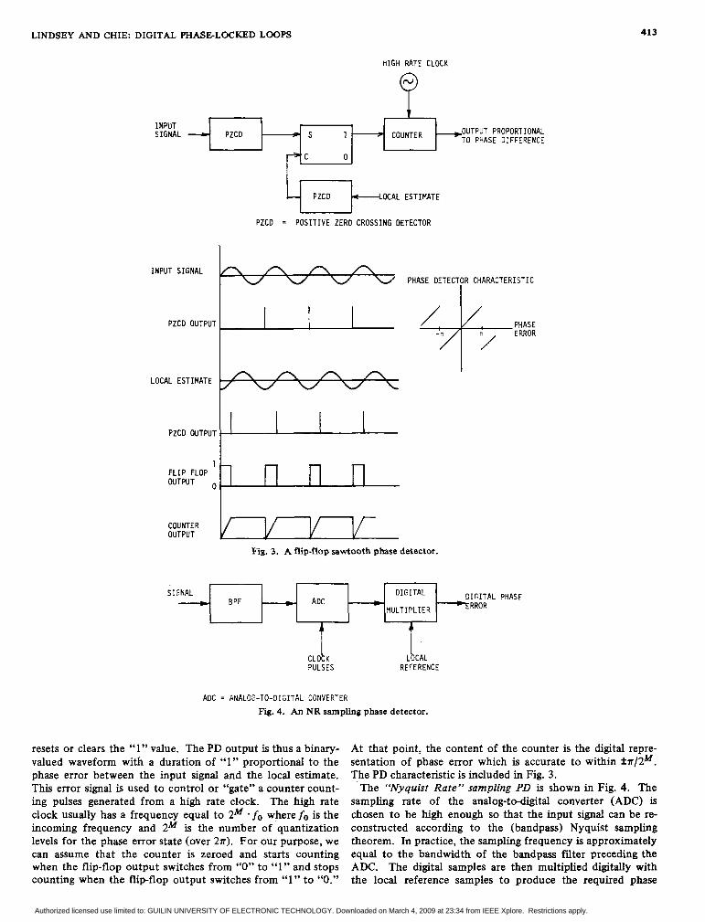
LINDSEY AND CHIE: DIGITAL PHASELOCKED LOOPS 413
HIGH RATE CLOCK
P INPUT SIGNAL - -OUTPUT PROPORTIONAL COUHTER - > s PZCD TO PHASE DIFFERENCE - e’ c 0
4 F k O C A L ESTIMATE
PZCD = POSITIVE ZERO CROSSING DETECTOR
INPUT SIGNAL PHASE DETECTOR CHARACTERISTIC
I
LOCAL ESTIMATE M I
COUNTER OUTPUT
Fig. 3. A flip-flop sawtooth phase detector.
CLO t K T PULSES RFFERENCE
LOCAL
ADC ANALOG-TO-DIGITAL CONVERTER
Fig. 4. An NR sampling phase detector.
resets or clears the “1” value. The PD output is thus a binary- valued waveform with a duration of “1” proportional to the phase error between the input signal and the local estimate. This error signal is used to control or “gate” a counter count- ing pulses generated from a high rate clock. The high rate clock usually has a frequency equal to 2M * fo where fo is the incoming frequency and 2M is the number of quantization levels for the phase error state (over 271). For our purpose, we can assume that the counter is zeroed and starts counting when the flip-flop output switches from “0” to “ 1 ” and stops counting when the flip-flop output switches from “1” to “0.”
At that point, the content of the counter is the digital repre- sentation of phase error which is accurate to within * ~ / 2 ~ . The PD characteristic is included in Fig. 3.
The “Nyquist Rate” sampling PD is shown in Fig. 4. The sampling rate of the analog-to-digital converter (ADC) is chosen to be high enough so that the input signal can be re- constructed according to the (bandpass) Nyquist sampling theorem. In practice, the sampling frequency is approximately equal to the bandwidth of the bandpass filter preceding the A N . The digital samples are then multiplied digitally with the local reference samples to produce the required phase
Authorized licensed use limited to: GUILIN UNIVERSITY OF ELECTRONIC TECHNOLOGY. Downloaded on March 4, 2009 at 23:34 from IEEE Xplore. Restrictions apply.

414 PROCEEDINGS OF THE IEEE, VOL. 69, NO. 4, APRIL 1981
SAMPLE0 SIGNAL
CONTROLLED B Y LOCAL SMPLING INSTANTS
REFERENCE
SIGNAL INPUT
SAMPLING PULSES
ADC OUTPUT
Fi. 5. Positive zero crossing sampling phase detector.
SIGNAL I tlPUT TRANSITION
SELECTOR SAMPLE - ADC = PHASE ERROR
SAMPLINS'PULSES CONTROLLED B Y LOCAL REFERENCE
INPUT SIGNAL
SMPLING PULSE
AOC OUTPUT
TRANSIT10 SMPLE SELECTOR OUTPUT
4 I
Fig. 6. Positive and negative zero-crossing sampling phase detector.
error samples. For low+peed applications, the function of the crossing and is shown in Fig. 6 . To provide for the correct digital multiplier is often performed with a microprocessor, polarity of the phase error samples, the transition sample which also doubles as the loop fdter and digital clock. selector flips the sign of the samples according to whether a
samples on the positive zero crossings and is shown in Fig. 5 . The leud/lug sampling PD shown in Fig. 7 is characterized by This type of PD appears to be the simplest to implement the simple binary PD output indicating whether the local among all DPLL's. The second type samples on every zero reference leads or lags the input signal. In many ways, this is
There are two types of zero-crossing PD's. The fmt type positive or negative going transition is detected.
Authorized licensed use limited to: GUILIN UNIVERSITY OF ELECTRONIC TECHNOLOGY. Downloaded on March 4, 2009 at 23:34 from IEEE Xplore. Restrictions apply.

LINDSEY AND CHIE: DIGITAL PHASELOCKED LOOPS
TYPICAL BINARY PHASE DETECTOR r - - - - - - - - - - - -1
415
INPUT 'IGNAL
4 7 E L E A D
DETECTOR LAG DUMP T / 2 I I I L _ _ _ _ - - - - - - - :
LAG Fig. 7. Leadflag sampling phase detector.
t G1
r - - - - - - - -1 'k G2
I
'k G3
k k m y k = G x + G 1 x,+ G 1 1 x, ' ,=O %=O ~ - 0
(b) Fig. 8. Higher order loop filters. (a) Second order. (b) Third order.
similar to the positive zero-crossing PD with a binary quan- 2) Digital Loop Filters: The digital equivalent of the analog tized phase error output. However, because of the harsh integrating element such as a RC filter is a digital accumulator. quantization used, a sequential fiter is often used to smooth In Fig. 8(a), we show the block diagram of a digital loop fdter the correction voltage applied to step the local DCO. For this used in a second-order loop. The digital accumulator is Simply reason, we prefer to keep it as a separate entity. mechanized using an adder and a unit delay connected as Authorized licensed use limited to: GUILIN UNIVERSITY OF ELECTRONIC TECHNOLOGY. Downloaded on March 4, 2009 at 23:34 from IEEE Xplore. Restrictions apply.

416 PROCEEDINGS OF THE IEEE, VOL. 69, NO. 4, APRIL 1981
LEAD - N-CWNTER (Lead)
ADVANCE
'OR'
RESET ALL
COUNTERS -THREE
L A G ! c N-COUNTER C. RETARD ( L a g )
Fig. 9. N-before-M filter.
COMPARATOR OSCILLATOR OUTPUT
RESET COUXTER
* INPUT LEVEL N
( a ) COUNTER OUTPUT
( b ) CO~lPARATOR OUTPUT t-
Fig. 10. Block diagram of a typical digitally controlled oscillator.
shown in the figure. By employing two accumulators in tandem, one obtains a digital approximation to a double integrator as in Fig. 8(b). The construction extends obviously to higher order approximations.
For the LL-DPLL, a different class of digital fiiters called sequential filters are employed. Since the PD output is binary, the sequential filter is used to smooth out the fluctuations seen at the PD output. The name sequential filter implies that the output is not a linear function of a fixed number of inputs. Instead, the sequential fiiter observes the inputs for a variable duration of time and gives an output when a certain confidence limit on the input is established. This procedure is very similar to the sequential threshold test in estimation theory. A representative sequential filter is depicted in Fig. 9. The N-before-M filter operates as follows. Lead and lag inputs are accumulated separately in the N counters while boththe lead and lag inputs are accumulated in the M counter ( N < M < 2N). Assume initially that all three counters are reset. The random sequence of binary inputs continues until one of two conditions is met. 1) If one of the Ncounters in the figure fills up before or simultaneously with the M counter, then the corresponding output is produced, all three counters are reset, and the cycle begins anew. 2) If a total of M lead + lag inputs occurs before N inputs of either type (lead or lag), all registers are reset and no output is produced. The latter condition is most likely when the phase error is near zero.
3) Digitally Controlled Oscillator: DCO is basically a pro- grammable divide by N circuit. Its functional block diagram is depicted in Fig. 10. The output of a stable oscillator (usu- ally at a frequency M1 times the IF frequency where M1 determines the phase error resolution) is used to drive the counter which increased by one every clock cycle. The con- tent of the counter is compared with the input and when they are matched, the comparator puts out a pulse which serves to be the DCO output and to reset the counter. By varying the control input N , the DCO period can be controlled. A pictorial operation of the DCO is also given in Fig. 10.
4) Combined Digital Loop Filter and Digitally Controlled Oscillators: The functional implementation of the DCO and the digital loop filter can also be combined. For example, Pasternack and Whalin [ 8 ] describe a scheme that uses more than one internally generated frequency, and Larimore [ 1 1 ] describes a scheme that utilizes a microcomputer to achieve these two functions in software. The interested readers should consult [8]-[ 121, [59].
B. DPLL Implementation Examples The basic block diagram for a DPLL is given in Fig. 1 1 . The
input signal is sampled and compared with a reconstructed reference to produce digitized error samples which are pro- portional to their phase differences. These samples are filtered by a numerical algorithm (digital fiiter) and the corresponding
Authorized licensed use limited to: GUILIN UNIVERSITY OF ELECTRONIC TECHNOLOGY. Downloaded on March 4, 2009 at 23:34 from IEEE Xplore. Restrictions apply.

Authorized licensed use limited to: GUILIN UNIVERSITY OF ELECTRONIC TECHNOLOGY. Downloaded on March 4, 2009 at 23:34 from IEEE Xplore. Restrictions apply.

418 PROCEEDINGS OF THE IEEE, VOL. 69, NO. 4, APRIL 1981
P I I I
I
I
I I
I
1 I
I
I I I
I b. D1GITI.L
DIGITAL MIXER
COLlWTATInNS
- 1 - - - - - --I I
DIGITAL I FILTER
I
Fig. 13. An NR-DPLL described by Larimore [ 11 1.
-1 I
I I I I
- A
I I
I I I
RESET
CLOCK COllPARE I I
Fig. 14. A ZC, -DPLL described by Natali [ 171.
PHASE OFTECTOR LOOP FILTER r - - - - - - - - - - - --r - - - _ - - - - _ - _ _ _
I
I SAMPLER A C C W L A T E
( A N 1 OVER MTO SGN
rr I
(W Hz) I
I I
I I
r - - - - - - - - - - - - Eo- - -I I
I I
I c
L - - - - - _ _ - - _ _ - 1 - - - _ _ - - - - - - - J - 1
I
I TIMING CLOCK I 6 UPDATE
1 1
L061C 1 I
I
I
TD = SIGNAL PERIOD
Fii. 15. A ZC, -DPLL described by Holmes and Teneglia [ 31 1 -[ 33 1.
Authorized licensed use limited to: GUILIN UNIVERSITY OF ELECTRONIC TECHNOLOGY. Downloaded on March 4, 2009 at 23:34 from IEEE Xplore. Restrictions apply.

LINDSEY AND CHIE: DIGITAL PHASELOCKED LOOPS 419
I
TIMING I
S I W L I
ADO OR DELETE STABLE FIXE0 - 1
I I ONE CYCLE
- FREQ. OSC.
I - _ _ - - - J I - - - - - -
RETAR
BINARY PHASE SEQUENTIAL INPUT
Fig. 16. An LL-DPLL due to Ctssna and Levy [351, [36].
LOOP COMPONENTS
Variable Counter
I Loop F i l t e r
M u l t i p l i e r / Accunulator
Canbi ned OCO/ Loop F i l t e r
TABLE I SPEED OP RELEVANT DIGITAL INTEGRATED CIXcUrrS
STATE OF THE ART PERFORWCE FOR CRITICAL COMPONENTS
COWENTS
350 Miz Clock Frequency I ECL Logic Prescaler
50 M Sasples/Sec with 8 B i t I “Flash“ Converters Resolution
40 ns per Cabined Operation Monolithic LSI
8 MHz Clock 1-2 us/Instruction Tmical
is used “optimally” to estimate whether the local clock lags or leads the signal input. Other than that, the LL-DPLL is very similar to a ZCI-DPLL with a one-bit phase error resolution.
C. Hardware Considerations The majority of the DPLL’s built and reported upon thus far
have been designed for low-speed (low data rate, low IF fre- quency) applications such as subcarrier demodulation. An exception is described by Natali [201 in 1972. The DPLL operates at an IF frequency of 1.92 MHz, a sampling fre- quency of 384 kHz, and the DCO is driven by a 92.16 MHz frequency source to give a phase quantization error of 7.5 degrees (2 X 1.92/92.16). Why is this the case? One impor- tant reason is hardware (logic speed) limitations. Typical (off the shelf) state of the art specification of critical logic components are shown in Table I. For example, one can build a DCO that operates from a 350-MHz internal clock. For the same 7.5 degrees quantization error, one can work with a maximum IF frequency of 7.29 MHz. Since the ADC and loop fiiter both work faster than the IF frequency, the critical component that limits the high-speed application of DTLL is clearly the DCO. Notice that a combined DCO/loop fiiter mechanization using a microprocessor yields a lower speed yet. Projections for higher speed logic components are available [ 471 and it seems unlikely that a ten-fold improvement can be made in the next few years.
w. LINEAR ANALYSIS OF DPLL Due to the discrete nature of a DPLL, its operation must be
described by a difference equation. In this section, the z-trans-
- Fig. 17. The baseband model for DPLL.
form technique is employed to analyze the general tracking behavior of a DPLL. This analysis is not limited to a particular class of implementations; the various implementation tech- niques are reflected in the difference equations governing their behaviors. Under the tracking assumption, the phase error samples are small and the general nonlinear difference equa- tion can be approximated by a linear one which can be solved by the z-transform technique. Some words of caution: in order to interpret and apply the linear result in a meaningful way, one must verify judiciously whether the tracking assump- tion is violated in any way for a particular application. Other- wise, the z-transform technique is simply not applicable and the results obtained are at best questionable.
A. Baseband Model The baseband model for the general DPLL block diagram in
Fig. 1 1 of Section 111-B is given in Fig. 17. The phase detector characteristic g(*) and the equivalent noise samples are both
Authorized licensed use limited to: GUILIN UNIVERSITY OF ELECTRONIC TECHNOLOGY. Downloaded on March 4, 2009 at 23:34 from IEEE Xplore. Restrictions apply.

420 PROCEEDINGS OF THE IEEE, VOL. 69, NO. 4, APRIL 1981
TABLE II Z-TBANSFORMS OF VARIOUS UNIFORMLY SAMPLED PEW INPUTS
Phase Modulation
dependent on the particular loop implementation. How- ever, the loop fiter and the DCO represented by D(z) and z-l/(I - z-l) are common among all implementations. We have used z-l to denote the delay operator, i.e., z-'qk = 4k-1. As a compact notation for manipulating with sequences, we
define the twc-sided z-transform z{.} of a sequence {qk} to be
z{qk} = qkz-k (4-1) k= -m
and denote z{qk} by Q(z). with this notation, we can repre- sent the equation of operation of a DPLL compactly in terms of its local phase estimate
q z ) = - h
z - 1
and phase error
where it is to be understood that g [ @ ( z ) ] denotes Z{g(&)}. In this section, we shall assume that the DPLL is in the
tracking mode with a small phase error about a reference phase (which we assume to be zero without loss of generality). In this case, g(&) =g'(O) &. Furthermore, we assume that g'(0) = 1 since we can lump the gain g'(0) with the loop filter F(z) . Using this assumption, one arrives at the linear loop equation for the phase error
@ ( z ) = [ 1 - H(z)l $(z) - H(z) - N(z ) (4-4) rn
where
H ( z ) = D(z)
(2 - 1) + D(z)'
B. Linear Tracking in the Absence of Noise
mined from the input phase samples {&}, namely, In the absence of noise, the phase error (&} can be deter-
@(z) = [ 1 - H(z)l @(z) (4-5 1
using the inverse z-transform. In what follows, we shall con- centrate on the special but important second-order loop (i.e., D(z) = G1 + Gz /( 1 - z-l)) with the normalized parameters
1 - H(z) = (2 - 1)Z
( z - a)Z + 8 2 . The corresponding difference equation is
k = 0, 1, - - (4-7)
with initial conditions &l = r#+ = 0 if we assume the DPLL starts at time t = 0 with zero initial states. For sampling with period T, the phase error transients to a phase step, a fre- quency step and a frequency ramp are summarized in Tables I1 and 111.
The impulse response of a homogeneous difference equation is a sampled version of the corresponding differential equation. In particular, if we let
-Sun T
-Sun T a = e cos (w, T d m ) P = e sin ( o , T d m ) (4-8)
the filter H(z) is equivalent to its analog counterpart
H(s) = 2{w, s + w:,
f Z + 2{,s + w:,
with normalized natural frequency w, and damping ratio {. The phase error transient responses are plotted in Figs. 18-20 in terms of { and w, T. In Fig. 2 1, we compare the phase error responses of the APLL and DPLL to a phase step. It is evident that as o , T +. 0, the phase error response of the DPLL is a sampled version of the analog one. As a matter of fact using (4-8) and Table 111, one can check that, in the limit as w,T --f 0, all responses are identical with the analog loop responses [ 481.
For sinusoidal phase modulation (PM)
O(t) = A0 sin w,t (4-9 1 and for sinusoidal frequency modulation (FM)
A U urn
e ( t ) = - cos W,t (4-1 0)
Authorized licensed use limited to: GUILIN UNIVERSITY OF ELECTRONIC TECHNOLOGY. Downloaded on March 4, 2009 at 23:34 from IEEE Xplore. Restrictions apply.

LINDSEY AND CHIE: DIGITAL PHASELOCKED LOOPS 421
TABLE I11 TRANSIENT PHASE ERROR {@t) OF SE-ER LOOP
PHASE STEP (eo radians) FREQUENCY STEP ("0 rad/sec) FREQUENCY RACP (nl rad/sec) I
.]1-m k [cos ke+ 2- 2 sin k j -
I (1 i k[cosh k(
where Ad denotes peak phase deviation, AU denotes the peak where frequency deviation, and U, denotes the modulation fre- quency, the steady-state phase error response is simply the = Z{E(nlnI*+k)} steady-state frequency response of (44). In P ~ C U ~ U , for PM is the z transform of the noise autocorrelation function. ~n
#k = 11 - H(UmT)l Ad (kU,T + 9) (4-1 1) many practical cases, we can model { n k ) to be uncorrelated zero mean with variance 17; = N o Bi (Bi is a bandwidth asso- ciated with the noise variance and is usually the bandwidth of the IF filter preceding the DPLL). The one-sided loop band-
whereas for FM AU Urn width BL is conveniently defined to be
#k = 11 - H(Um T)I - COS (kUm T + JI) (4-1 2)
where the gain I1 - H(u, T)l and the phase shift JI are deter- mined from 2 BL /Bi = - j H ( z ) H(z-' ) z-' dz. (4-16)
This yields u$ = NO BLIP which is identical with the analog
2nj 11 - H(Wm T)I eW [ 1 - H(z)l , = exp (jw, q. (4-1 3)
Explicitly, we have result.
11 - H(u,T)I= 4 sinz (0, T/2)
{ ~ C O S ~ U ~ T ~ ~ U C O S U ~ T + ( U ~ + ~ ~ ) ] ~ + [ S ~ ~ ~ U , T ~ ~ U ~ ~ ~ U , T ] ~ } ' ~ ~
and The evaluation of the integral
JI = n + tan-' (wrnT)
- tan-' s i n 2 0 , T - 2 a s i n ~ , T
COS~U,T- 2acosw,T+(uZ + 8 2 ) I- ... . -
is tabulated in [SO, pp. 297-2991. For future reference, the (4-14) results for the first- and second-order DPLL is reproduced in
The behavior of the steady-state phase error response as a Table Iv. function of the normalized parameter f and u,/u, are plotted in Figs. 22 and 23.
C. Linear Tracking in the Presence of Noise
steady-state variance of {&} is given by [ 491
D. Relationship of Linear DPLL to Linear APLL
If the DPLL is in the tracking mode and the phase error is small (u$ << 1) so that the h e a r approximation applies, it is
If the noise samples { n k } are stationary with mean zero the to that
' P 0; = - H(z) H(2- I ) 2-l ff,(z> dz (4-15) 0, = e(kT) (4-1 8)
2ni 2P where T is the nominal clock period. In that case H(z) can be
Authorized licensed use limited to: GUILIN UNIVERSITY OF ELECTRONIC TECHNOLOGY. Downloaded on March 4, 2009 at 23:34 from IEEE Xplore. Restrictions apply.

422 PROCEEDINGS OF THE IEEE, VOL. 69, NO. 4, APRIL 1981
interpreted as a continuous filter HJw), viz.
HJO) = H(z)l,=exp ( jwT)
a low-pass fiter with a bandwidth BL << 1/T, then the DPLL approximates an APLL for
(e.g., see [ S O ] ). Furthermore, if H ( z ) is designed primarily as z = 1 + j o T , for UT<< 1. (4-19)
Authorized licensed use limited to: GUILIN UNIVERSITY OF ELECTRONIC TECHNOLOGY. Downloaded on March 4, 2009 at 23:34 from IEEE Xplore. Restrictions apply.

LINDSEY AND CHIE: DIGITAL PHASELOCKED LOOPS 423
1.5 ,. w,T = 0.1
. e * . .
. . . * . * . . ...
. . . . . . . . . . . : . - ,!.
o - " " " " ' " " ' " " ' ~ ' ' " " " ~ ~ " ' ' ' ' ' ' 0 20 40 60 8
NUMBER OF STEPS, k
Fig. 20. Transient phase error due to a ramp in frequency a,.
0
0 2.0 4.0 6.0 8.0
w,t +
Fig. 21. Comparison of phase error responses of AF'LL and DPLL to a phase step B o .
Authorized licensed use limited to: GUILIN UNIVERSITY OF ELECTRONIC TECHNOLOGY. Downloaded on March 4, 2009 at 23:34 from IEEE Xplore. Restrictions apply.

424 PROCEEDINGS OF THE IEEE, VOL. 69, NO. 4, APRIL 1981
Fig. 22. Steady-state phase error due to sinusoidal PM.
Fig. 23. Steady-state peak phase error due to sinusoidal PM.
terestingly enough, equation (4-19) is also satisfied under this condition. It seems to imply that a DPLL must be designed to approximate an APLL in order to function properly.
V. THEORY OF ZEROCROSSING SAMPLING DPLL In this section, we shall focus on the zero-crossing sampling
DPLL and the ZCI-DPLL in particular. Our effort is justified for a number of reasons. First of all, this type of loops is the easiest to implement since a single ADC is needed for detecting the phase error. Because of this simplicity, a mathematical model can be developed with relative ease to describe its prin-
ciple of operation and to provide a basis for exact analysis, both in the deterministic and stochastic domain. Furthermore, the analytical results obtained from this type of DPLL em- body the essence of the operation of any DPLL. For this rea- son, they are also applicable for both loop types.
The block diagram of the ZC1-DPLL to be studied is de- picted in Fig. 24. The incoming signal is modeled via
The IF Gaussian noise n(r), obtained from bandpass filtering the AWGN of singlesided spectral density NoW/Hz , is band-
Authorized licensed use limited to: GUILIN UNIVERSITY OF ELECTRONIC TECHNOLOGY. Downloaded on March 4, 2009 at 23:34 from IEEE Xplore. Restrictions apply.
LINDSEY AND CHIE: DIGITAL PHASELOCKED LOOPS
TABLE IV A U r n INTKGRA~ON TABLE
4 2 5
I
I - I---- SAMPLER
DIGITAL FILTER I FILTER D(z)
-I-
Fig. 24. Block diagram of a DPLL.
f
Fig. 25. Operation of a f i i -order DPLL in the abscence of noise with e(r) = eo .
limited to Bi Hz and centered at the carrier frequency fo = Here the nominal clock period T is assumed to be an integral w0/27r. The incoming signal is sampled at time instants tk de- multiple of the period of the carrier, i.e., T = M / f o . Fig. 25 termined by the digital clock. The time elapsed between the illustrates the operation of the loop when d ( t ) = B o , and (k - 1)th and kth samples is denoted by D ( z ) = 1. The &'s in Fig. 25 are defined later on (see (5-6)).
For an Nth-&der loop, the digital filter D(z ) has the form (5-2) D(z) = z, N = 1 G,( 1 - z-l)-,+ 1 . From (5-2), to (5-4), it can
while the value of the incoming signal at tk is be shown that the loop is described by theNth-order stochas- tic difference equation [ 5 1 ]
X k = J k + n k , k = 0 , 1 , ' * ' . (5-3)
This sequence of signal samples {xk}, k = 0, 1, - * - is filtered and the filtered outputs ( Y k } , k = 0, 1, 2, * - * are used to con- trol the next period of the digital clock according to the fgorithm m = l
(1 - z-l)N #k = (1 - z - l ) N dk - w6- l
N C, (1 - {D @k + nk) .
T k + 1 = T - y k , k = 0 , l ," . . (5-4) (5-5) Authorized licensed use limited to: GUILIN UNIVERSITY OF ELECTRONIC TECHNOLOGY. Downloaded on March 4, 2009 at 23:34 from IEEE Xplore. Restrictions apply.

426 PROCEEDINGS OF THE IEEE, VOL. 69, NO. 4, APRIL 1981
TABLE V SUMMARY OF STOCHASTIC DIFFERENCE EQUATIONS FOR FIRST-, SECOND,
AND THIRDORDER DPLL'S
Received F i l t e r
Order S i g n a l e ( t ) o f Loop F u n c t i o n
T r a n s f e r
i e o + R o t k
D i f f e r e n c e E q u a t i o n
F i r s t I G1
+k+l'$k = -5 sip+k - ~ ~ i ; ~ + A 0
L .
i I
..................................................................... r L ...............................
= -K1r sin+k+l + K1 s i n + k
I - K2rEk+l + $4
1 8 + R o t k 1-BZ-1 Second
G1 + - I m p e r f e c t i o G2
$ k + 2 - (1+6)$k+1 +
= -Klr sin+k+l + KIE s i n $ k
I - K2'";(t1 + K2Brk + A o ( l - E ) .................................................................................................. 1 ' 0 + *Otk 1 Third 1 + G2 1' ! + k+3 - 4 k+2 + 9 k + l - + k
,no 4 Y - Y o
I
1 = -P? sinbi+2 + Kl( l+r )s in+k+l G, I
#.............I...........
0
, ..........................
.......................... 0
i 1 I I
Fig. 26. Equivalent baseband model of the ZC, -DPLL.
In (5 -5 ) , the phase error $k is defined by
( e o 9 k = O
and represents the error in the loop estimate
of the input phase 6,. The mathematically equivalent model of the DPLL is depicted in block diagram form in Fig . 26. Equations of operation of the important examples of the fmt-, second- and third-order loops are summarized in Table V. The steadystate error can be determined from the difference equa- tion by setting #k equal to #*. The definition of constants used is given in Table VI.
A . A Summary of Results From the Linear Model A number of important properties of the DPLL can be de-
duced from linearizing the loop equation. The resultant h e a r model can be used to determine the closed loop transfer func- tion, to establish the stability region (locally), to determine
TABLE VI DEFINITIONS OF CONSTANTS
QUANTITY
K1 = WG1m t$ = w G 2 m
w = no t wo
r = 1 + $/G1
p = 1 + G2/G, + G3/G1
A0 GOT
;ik = n k / / Z P
Rad/vol t
Rad/ sec
--
the loop bandwidth, and to compare with the analog results. In Tables VI1 and W I , these results are provided for cases of practical interest.
B. Nonlinear Theory of ZC1 -DPLL Whereas the linear model provides us with information about
the operation of a DPLL operating in the .tracking mode, cer- tain questions remain unanswered. Most noticeably, it does not describe adequately the behavior of the loop in the acquisition mode where its operation is definitely nonlinear. In addition, when the DPLL is operating near its threshold, one would also like a refinement of the phase jitter predicted by the linear theory, as well as an understanding of the cycle slipping phenomenon [2], [48].
I ) Loop Operation in the Absence of Noise: With nk 5 0, certain general properties of the iterative scheme defined by (5 -5) can be determined using well known results from (func- tional) analysis [461, [521-[541, [621, [631. These results are generally known as contractive-mapping and fixed-point theorems. (These theorems are applicable to an arbitrary phase detector characteristic, i.e., the function sin (.)is being replaced
Authorized licensed use limited to: GUILIN UNIVERSITY OF ELECTRONIC TECHNOLOGY. Downloaded on March 4, 2009 at 23:34 from IEEE Xplore. Restrictions apply.

LINDSEY AND CHIE: DIGITAL PHASELOCKED LOOPS 427
TABLE VI1 LINEARIZED Loop EQUATIONS AND CLOSED Loop TRANSFW FUNCTIONS
j Type of I
Loop L i n e a r i z e d E q u a t i o n I Closed Loop
1 T r a n s f e r F u n c t i o n H(z)
1 F i r s t Oktl = +k - K1 s i n e t - Kl(+k- Ot)cos 0,
j l I 1 i 1 /, . ';;c.o.n.;l. !I
I
KCik + A o - K
= ek - - OL)COS 0,. - K rk z - 1 t K1 cos +t
1 ......................................... ......................................................................... i ~
i
( O r = s i n - ' 10)
+ k t 2 - '+kt1 ' + k K 2 ( - r z t 1 ) ' z2 t (K1r -2 )z + (1 - K1)
I
I = ' K I N k t l t K l $ k - KZrrk+l $ r k ................................................................................................................................ I i
I m p e r f e c t Second ' k t 2 (ltBN k t 1 ' @ k i
1
= -K1r(Oktl - O t ) cos Ot+KIB(+k - OP)COS + , I K2(-r2 + 8 ) 1
(2' t [K1r cos - ( 1 + 6 ) l z t ( 8 - KlBcos $)I - K 2 r rktl t K$Zk -1 b ( 1 - 6 ) I ~
= s i n K,(';8) I .............................................................................................................................. T h i r d -0 tt3 - 3+kt2 t )+kt1 - % i
~ ~ ~ [ - p z ' t ( l + r ) z - 11 -PKf k t 2 ' K1 (l'rk k t 1 K l $ k
TABLE VLII PROPERTIES OF LINEARIZED LOOP
I TYPE OF LOOP I STABILITY REGIOII 1 LOOP BANWIDTH. ZB,/B, I COMPARISON YIM APLL
by any g(-).) To summarize in our terminology, they guaran- tee: (a) a lock point exists if the "norm" of the "state" of the DPLL decreases at each step (b) the rate of convergence to the lock point is related to the reduction in norm at each step (c) the local stability behavior about the lock point can be deter- mined by the stability of the linearized equation' and (d) a quadratic rate of convergence can be achieved by setting the loop parameters so that the next state of the linearized loop is zero at the lock point. As an example, we consider the first- order loop with detuning & = 0. We shall choose the state of
that the state of an Nth-order loop is defined by N consecutive phase samples.) Then from Table V, ( @ k + I = l@k - K1 sin @kl G if I 1 - K11< 1. From (a), t t , Astence of a lock point @* = 0 is guaranteed. Furthermore, we have I@k+ll < 11 - K1l'l@kl from (b). Using (c), the linearized equation is @kt = (1 - KI @k ; hence, near the lock point the loop is stable if I1 - K1 I < 1 and unstable otherwise. Finally, from (d), we know that a choice of K1 = 1 yields quadratic convergence.
Although the above theorems supply us with a general pic- ture of the behavior of the DPLL, they have one main draw- back: they do not provide us with a method to construct a
the loop to be @k and its to be l@k - 01 = l@kl. (Note
' For a more precise mathematical statement, see [ 62 1, [ 63 1.
convenient norm for higher order loops (except the obvions choice for a first-order loop as indicated in the example). In general, one must rely on a phase-plane technique and direct simulation to determine the requirements for global stability and to study the acquisition behavior. Basically, these methods are graphical aids to describe the behavior of the DPLL. Ex- amples based on the phase-plane technique to study detailed loop stability for first-order and higher order loops can be found in (181, [191, [271, [ B I , [461, [S l l , [621, [631.
The concept of acquisition time is worth mentioning as it characterizes the acquisition behavior of the loop. The first acquisition step ko is defined as the number of steps past be- fore the loop phase error remains within E of the lock point given a starting state. The acquisition time T , is approximately given by T , = koT/(l +Slo/o0), 1271, which is of course a function of the initial state.
2) Loop Operation in the Presence of Noise: In most prac- tical implementations, the nominal sampling frequency f, = l /T is designed to be very close to the bandwidth of the IF filter Bi. In that case, the noise sequence can be approximated by a sequence of independent and identically distributed Gaussian random variables with mean zero and variance
0: = BiNo. (5-7)
Even with this approximation, the stochastic difference equa- Authorized licensed use limited to: GUILIN UNIVERSITY OF ELECTRONIC TECHNOLOGY. Downloaded on March 4, 2009 at 23:34 from IEEE Xplore. Restrictions apply.

PROCEEDINGS OF THE IEEE, VOL. 69, NO. 4, APRIL 1981
K, = 0.2
" a 0
Palog pLL Theor? Numerical Solution to C-K Equation
Second-Order Approximation
Linear Approximation
0.00 2.00 4.00 6 . 0 0 8.00 10.00 P (-1
F'ig. 27. Comparison of the steady-state variance from numerical solu- tion and fmt- and second-order approximation for a fmt-order DPLL.
tion (5-5) is non-Markovian for second-order and higher order loops. However, it is always possible [46], [55] to introduce a hear mapping for the phase error samples so that the trans- form equation takes the form
x k + 1 = f ( x k ) + nk c (5 -8)
where x k is an N-vector with the first component equal to & , f is an N X N matrix function and c is a column vector. Clearly, equation (5 -8) is Markovian since at each step, the state variable x k is corrupted by the noise sample nk which is inde- pendent from one step to the next. The conditional PDF of x k + conditioned on the initial state x . satisfies the Chapman- Kolmogorov (C-K) equation
Pk+l(Xk+llXO)= 4(Xk+11U)Pk(UlxO)du (5-9) I where the integral is def ied over the whole space of the n- vector u, Pk(XkIx0) is the conditional PDF of xk given x0 and &k+ l lu) is the transition PDF of x k + given xk = U. For theoretical and practical considerations, it is convenient to r e strict the phase error #k to modulo 2n [ 261. Examples of the C-K equation for the first- and second-order loop can be foundin [24] and [S l ] .
Equation (5-9) describes the complete statistical behavior of the state vector xk (and hence its first component & ) at each sample time if the initial PDF for x . is given. In addition, a steady-state PDF p J x ) for ( x k } always exists [ 261 and is given by the solution to the integral equation
(5-10)
A numerical technique for solving (5-10) for the first- and second-order loop is described by [24] while an analytical solution based on Fourier series expansion is given in [ 261, [ 5 1 ] . Plots of the steady-state phase error PDF as well as steady-state phase jitter are included in these references. As a footnote, second-order approximations for computing
the steady-state phase error variance are also available for f i t - and second-order loops [ 241, [Sl] . They are based on trun- cating the series expansion sin (I$) = 4 - $3/3! + - - * and are tight for a loop signal-tenoise ratio greater than 4 dB. A com- parison of steady state variances for a first-order loop is given in Fig. 27. ( p 5 P c / N o B ~ and BL is given in Table VIII.)
The problems of signal acquisition and cycle slipping can also be studied using the C-K equation with minor modifica- tions. To model signal acquisition, an absorbing well is placed around the lock point and for cycle slipping, absorbing barriers are placed at f2n. The C-K equation now applies to the re- maining probability at each step. For first- and second-order loops, the signal acquisition probability, the mean time to ac- quire, the cycle slipping probability and the mean time to f i t cycle slip have been obtained using this approach [ 241 , [ 271, [ 5 1 1 . Numerical results are also available in these references.
Although the theoretical results based upon the C-K equa- tion approach have been useful in evaluating the performance of the first- and second-order DPLL's, they are rather difficult to obtain computationally. This is especially the case for high loop signal-tenoise ratios. Due to its discrete nature, direct computer simulation of the stochastic difference equation de- scribing the operation of a DPLL is, however, simple and rather economical. This approach is especially recommended if a new loop c o n f i a t i o n is to be tested out.
Authorized licensed use limited to: GUILIN UNIVERSITY OF ELECTRONIC TECHNOLOGY. Downloaded on March 4, 2009 at 23:34 from IEEE Xplore. Restrictions apply.

LINDSEY AND CHIE: DIGITAL PHASELOCKED LOOPS 429
Fig. 28. Equivalent baseband model with quantization function Q(z ) restricted to produce integer outputs.
U Fig. 29. Block diagram of an Nth-power DPLL for suppressed carrier
tracking.
C. Quantization Errors So far we have neglected the quantization errors involved
with the finite bit length of the ADC and the discrete nature of the DCO. In reality the sampler output is quantized to rn Q[sin (4k) + n k / r n ] where e (* ) is the quantization function with its range of integer values. In addition, the DCO can only change its period in increments of TIM where M is the resolution of the DCO (ratio of internal clock to IF fre- quency). The quantization effect of the DCO can be studied [ 221 via assuming that the digital filter D(z) can only generate integer valued outputs, i.e., the gains Gi are integers. In that case the equation of operation for an Nth-order loop is given by
(1 - z - ~ ) ~ @ ~ = (1 - z -1 N ek - 2" f ~ , ( 1 - Z-l)N-m+l Qbin 4k + &I.
(5-1 1)
The baseband equivalent block diagram is illustrated in Fig. 28.
The behavior of the quantized loop in the absence of noise can be studied via the phase-plane technique and the general theory mentioned earlier since the inclusion of quantization error serves only to modify the phase detector characteristic from sin (@) to Q[sin (@)I (e.g., see [281). In the presence of noise, the C-K equation still holds. However, since the phase steps take on discrete increments, the C-K equation can be re- duced to the equation of transitional probabilities for Markov
M m = 1
chains. The utility of the theory of Markov chains in the anal- ysis of DPLL with quantization effect is illustrated in [ 3 1 ] for a fiit-order loop.
As a general rule of thumb, a 3-bit ADC seems to approach the performance of an ADC with infii te quantization [ 5 1 1 . In addition, the quantization effect of the DCO can be ac- counted for approxmaiely by including an additional inde- pendent white noise term with a variance equal to (2n/M)'/12 in the analysis [33].
VI. DIGITAL PLL FOR SUPPRESSED CARRIER RECOVERY
We now highlight some recent ZC1-DPLL structures devel- oped [561 for the reconstruction of the carrier phase of poly- phase signals [ 571 employed extensively in digital communica- tion systems. A detailed description and analysis is given in [461, [ 621 , [ 63 I . A slightly different implementation for tracking biphase modulated carrier has been reported earlier by Natali [ 201.
The first configuration proposed for suppressed carrier re- covery, the digital Nth-power loop, is an immediate extension of the digital loop presented. However, the implementation of the second model, the digital N-phase I-Q loop represents a new approach to the development of digital suppressed carrier loops. The stochastic difference equations which characterize the loop operation for these two models are equivalent under certain special conditions. In any case, they are very similar to the ones that we have seen in the last section. (In principle, the main difference between a CW and a suppressed carrier DPLL is in the structure of the phase detector characteristic, i.e., g(-) in Fig. 17.)
Authorized licensed use limited to: GUILIN UNIVERSITY OF ELECTRONIC TECHNOLOGY. Downloaded on March 4, 2009 at 23:34 from IEEE Xplore. Restrictions apply.

430 PROCEEDINGS OF THE IEEE, VOL. 69, NO. 4, APRIL 1981
EXTRACTIW
A
DATA
EXTRACTICM DATA
Fii. 30. Implementation of digitat N-phase ZQ loop.
A. The Nth Power DPLL Functional Model
A functional diagram of the Nth-power DPLL is shown in Fig. 29. As can be seen, the incoming modulated signal plus noise w ( t ) is filtered, raised to the Nth power to remove the phase modulation,. and then filtered again in a zonal filter to isolate the Nth harmonic. Thus the resulting signal x ( t ) into the digital loop consists of a signal term, viz. a carrier compo- nent at Nfo (fo is the frequency of the incoming signal), and a noise term composed of signal X noise and noise X noise products.
B. The N-Phase Digital Z-Q Functional Model
One implementation of this digital Z-Q loop is shown in Fig. 30; this is the loop that is closest in characterization to the Nth-power loop, and is in fact the optimum loop for low signal-to-noise-ratio operation. In the model of Fig. 30, the incoming signal is filtered by H&), and then split into the Z and Q projections at another frequency by a free-running oscillator. The effects of the filter Hi(#) and the arm filter HI(#) can be mathematically lumped together since the filters are in sequence. The sampled Z and Q signals are then filtered again by F(z ) , and processed to form the error signal x k . For example, if N = 2, the mathematical operation needed to generate x& is simply ZkQk/2 and can be replaced by a multiplier. In that case, Fig. 30 is very similar to an analog Costas loop. Considerable analytical work has been carried out in [46].
ACKNOWLEDGMENT
The authors would like to express their appreciation to Drs. H. C. Osborne, W. R. Braun, and C. R. Cahn for their review of the manuscript and valuable suggestions.
REFERENCES
[ 1 ] S. C. Gupta, “Phase-locked loops,”Roc. IEEE, vol. 63, pp. 291- 306. Feb. 1975.
W. C. Lindsey, Synchronization Systems in Communkution and Control. Englewood Cliffs, NJ: Prentice-Hall, 1972. F. M. Garbs. phase Lock Techniquw, 2nd ed. New York: Wiley, 1979. P. R. Westlake, “Digital phase control techniques.’’ IRE Truns. Commun. Syst., vol. CS-8. pp. 237-246, Dec. 1960. C. J. Byme, “Propaties and design of the pharccontrolled os- cillator with a sawtooth comparator,” Bell Syrt. Tech. J.. vol. 41,
S. C. Gupta, “On optimum digital phase locked loops.” ZEEE Tmm Commun. Technol., vol. COM-16. pp. 340-344, Apr. 1968. E. M. Drogin. ‘‘Steaing on course to safes air travel,”Electron.,
G. Pasternack and R. L. Whaiin, ‘‘Andy& and s y n t h d of a digi- tal phase locked loop for FM demodulation,”Bell Syst. Tech. J.,
H. Goto, “A digital-phase locked loop for.synduonizing digital networks,” in ROC. Znt. Conf. Communications. June 1970. M. Yamashita e t al., “Jitter reduction of a phase-locked loop,”
W. E. Larimore, ‘‘Syntheek of digital phase-locked loop,” in 1968 EASCONRec., pp. 14-20, Oct. 1968.
Communications (Polytech. Inat. of Brooklyn, New York) pp. locked loop,” presented at the Symp. Computer Processing in
J. Greco, J. Garodnick, and D. L. Schilling, “An all digital phase locked loop for FM demodulation,” in Roc. Znt. Con$ Commu- nications, June 1972.
Conf.,vol. VIII, pp. 119-123, Oct. 1972. J. Greco and D. L. Schilling, “An all digital phase locked loop for FM demodulation,” in Roc. Znr. Conf. Communications, pp.
J. Garodnick, J. Grew, and D. L. Schilling, “Response of an all 43:37-43:41, June 1973.
digital phase-locked loop,” IEEE Tram Commun. Technol., vol. COM-22, pp. 75 1-764, June 1974.
s igna ls ,” in 1968 EASCON Rec., pp. 407-412, Oct. 1968. F. D. Natali, “Accurate digital detection of angle modulated
loop with applications to demodulation of angle-modulated car- G. s. Gill and S. C. Gupta, “First-order discrete phase-locked
rier,” lEEE Tmnr. Commun. Technol., vol. COM-70, pp. 454- 462, June 1972.
locked loops,” ZEEE Trans. Aerosp. h7ectrorr mat., vol. A B S , G. S. Gill and S. C. Gupta, “On higher order discrete phase-
Roc. Znt. Telemetering Conf., vol. VIII, pp. 89-108, Oct. 1972. F. D. Natali, “AU digital coherent demodulator techniques,” in
C. P. Reddy and S. C. Gupta, “Demodulation of FM signals by a
VLII, pp. 124-133, Oct. 1972. discrete phase-locked loop,” in Roc. Znt. Telemetering Conf., vol.
pp. 559-602, Mar. 1962.
pp. 95-102, NOV. 27,1967.
pp. 2207-2237, DeC. 1968.
ROC. IEEE,vol. 64, pp. 1640-1641, NOV. 1976.
- , ‘‘Design and performance of a second-orda d- phaae-
343-357, AP. 8-10.1969.
- , “An all digital phase locked loop,” in Roc. Znt. Telemetering
pp. 615-623, Sept. 1972.
- , “A class of all digital phase locked loops: Modeling and anal-
Authorized licensed use limited to: GUILIN UNIVERSITY OF ELECTRONIC TECHNOLOGY. Downloaded on March 4, 2009 at 23:34 from IEEE Xplore. Restrictions apply.

LINDSEY AND CHIE: DIGITAL PHASELOCKED LOOPS 431
[ 2 3 ] -, “An all digital phase locked loop for synchronization of a ysis,” inProc. Nut. Telecommun. Conf., pp. 326:l-7, Dec. 1972.
sinusoidal signal embedded in white Gaussian noise,” in Proc. Nut. Telemetering Conf., Nov. 1974.
[ 2 4 ] k Weinberg and B. Liu, “Discrete time analyses of non-uniform sampling first- and second-order digital phase-lockedloops,”IEEE
[ZS] T. Koizumi and H. Miyakawa, “Statistical analyses of digital Trans. Commun. Technol., vol. COM-22, pp. 123-137, Feb. 1974.
phase-locked loops with time delay,”IEEE Trans. Commun., vol. COM-25, pp. 731-735, July 1977.
[ 2 6 ] C. M. Chie, “Mathematical analogies between fist-order digital and analog phase-locked loops,” IEEE Trans. Commun., vol.
[ 2 7 ] W. C. Lindsey and C. M. Chie, “Acquisition behavior of a fsst- COM-26, pp. 860-865, June 1978.
order digital phase-locked loop,” IEEE Trans. Commun., vol. COM-26, pp. 1364-1370, Sept. 1978.
[ 2 8 ] N. A. D’Andrea and F. R w o , “A binary quantized digital phase- locked loop: A graphical analysis,” IEEE Trans. Commun., vol.
[ 2 9 ] F. Russo, “Graphical analysis of a digital phase-locked loop,” COM-26, pp. 1355-1364, Sept. 1978.
IEEE Trans. Aerosp. Electron. Syst., vol. AES-15, pp. 88-94, Jan. 1979.
[ 301 L. F. Rocha, “Simulation of a discrete PLL with variable param- eters,”Proc. IEEE, vol. 67, pp. 440-442, Mar. 1979.
[ 3 1 1 J. K. Holmes, “Performance of a fist-order transition sampling digital phase-locked loop using random-walk models,” IEEE
[ 32 1 C. R. Tegnelia, “A simple second-order digital phase-locked loop,” Commun. Technol., vol. COM-20, pp. 11 9-1 3 1, Apr. 1972.
in Proc. Int. Telemetering Conf., vol. VIII, pp. 108-118, Oct. 1972.
[ 33 1 J . K. Holmes and C. R. Tegnelia, “A second-order all digital phase- locked loop,” IEEE Trans. Commun. Technol., vol. COM-22, pp.
1341 J . R. Lesh, “Calculating acquisition behavior for completely digi- 62-68, Jan. 1974.
45, 1975. tal phase-lock loop loops,’’ JPL DSN Prop. Rep. 42-39, pp. 33-
[ 351 J. R. Cessna and J. D. M. Levy, “Phase noise and transient times for a binary quantized digital phase-locked loop in white Gaussian noise,” IEEE Trans. Commun. Technol., vol. COM-20, pp. 94-
] J. R. Cessna, “Digital phase locked loops with sequential loop 104, Apr. 1972.
filters: A case for coarse quantization,” in h o c . Int. Telemetering Conf., vol. VIII, pp. 136-148, Oct. 1972.
] A. Yamamoto and S. Mori, “Performance of a binary quantized
IEEE Trans. Commun., vol. COM-26, Jan. 1978. all digital phase-locked loop with a new class of sequential filter,”
1 C. N. Kelly and S. C. Gupta, “The digital phase locked loop as a near optimum FM demodulator,”IEEE Trans. Commun. Technol., vol. COM-20. DD. 406-411. June 1972.
(391 -, “Discretdtime demodulation of continuous time signals,” IEEE Trans. Inform. Theory, vol. IT-18, pp. 488-493, July 1972.
[ 4 0 ] D. R. Polk and S. C. Gupta, “Quasi-optimum digital phase-locked loops,” IEEE Trans. Commun. Technol., vol. COM-21, pp. 75-
[ 4 1 ] -, “An approach to the analysis of performance of quasi- 82, Jan. 1973.
optimum digital phase-locked loops,” IEEE Trans. Commun. Technol., vol. COM-21, pp. 733-738, June 1973.
[ 4 2 ] A. L. McBride, “On optimum sampled-data FM demodulation,’’ IEEE Trans. Commun. Technol., vol. COM-21, pp. 40-50, Jan. 1973.
1431 G. T. Hurst and S. C. Gupta, “Quantizing and sampling consid- erations in digital phase locked loops,” IEEE Trans. Commun. Technol., vol. COM-22, pp. 68-72, Jan. 1974.
[ 4 4 ] G. T. Hurst and S. C. Gupta, “On the performance of digital phase locked loops in the threshold region,” IEEE Trans. Commun. Technol., vol. COM-22, pp. 724-726, May 1974.
1451 A. Weinberg and B. Liu, “Digital phase lock for optimum de- modulation,” IEEE Trans. Aerosp. Electron. Syst., vol. A E S l l ,
[46] H. C. Osborne, “Theory of digital phase-locked loops for sup- pressed carrier recovery,” Ph.D. dissertation, Univ. Southern
[47] B. G. Bosch, “Gigabit electronics-A review,” Proc. IEEE, vol. California, Los Angeles, Feb. 1979.
[48] H. Meyr, “Nonlinear analysis of correlative tracking sys tem
vol. COM-23, pp. 192-203, Feb. 1975. using renewal process theory,” IEEE Trans. Comrnun. Technol.,
[ 4 9 ) A. V. Oppenheim and R. W. Schafer, Digital Signal Processing.
[ S O ] E. I. Jury, Theory and Application of the z-Transform Method. Englewood Cliffs, NJ: Prentice-Hall, 1975.
[ 5 1 ] C. M. Chie, “Analysis of digital phase-locked loops,” Ph.D. disser- Huntington, NY: Robert E. Krieger Publishing Co., 1973.
tation, Dep. Elec. Eng., Univ. Southern California, Los Angeles, Jan. 1977.
[52] E. K. Blum, Numerical Analysis and Computation: Theory and Practice. Reading, MA: Addison-Wesley, 1972, ch. 1, 5.
I531 J. M. Ortega, Numerical Analysis: A Second Course. New York: Academic Press, 1972, ch. 1 , 8.
(541 P. Henrici, Elements of Numerical Analysis. New York: Wiley, 1964.
1551 L. A. Zadeh and C. A. Desoer, Linear Systems Theory. New York: McGraw-HiU, NY, 1963.
[561 W. C. Lindsey and H. C. Osborne, “Digital phase-locked loops for suppressed carrier recovery,” NTC, Washington, DC, Nov. 1979.
[ 5 7 ] W. C. Lindsey and M. K. Simon, Telecommunication Systems Engineering. Englewood Cliffs, NJ: Prentice-Hall, 1973.
[5Sl W. C. Lindsey and M. K. Simon Eds., Phaselocked Loops and Their Applications. New York: IEEE Press, 1978.
[ 591 C. R. Cahn and D. K. Leimer, “Digital phase sampling for micro- computer implementation of carrier acquisition and coherent tracking,” IEEE Trans. Commun. Technol., vol. COM-28, pp.
1601 N. A. D’Andrea and F. Russo, “Multilevel quantized PDLL be-
pp. 1269-1280, NOV. 1975.
67, 1979, pp. 340-379.
1190-1 196, Aug. 1980.
61
62
63
I
havior with phase- and frequency-step plus noise input,” IEEE Trans. Commun. Technol., vol. COM-28, pp. 1373-1382, Aug. 1980.
1 C. M. Chie, “A second-order frequency-aided digital phase-locked loop for Doppler rate tracking,” IEEE Trans. Commun. Technol.,
11 H. C. Osborne, “Stability analysis of an Nth power digital phase- locked loop-Part I: First-order DPLL,” IEEE Trans. Commun. Technol., vol. COM-28, DD. 1343-1354. Aue. 1980.
V O ~ . COM-28, pp. 1431-1436, Aug. 1980.
I ] -, “Stability analys’g -of an Nth pow& digital phase-locked loop-Part 11: Second- and third-order DPLL’s,” IEEE Trans. Commun. Technol., vol. COM-28, pp. 1355-1364, Aug. 1980.
1641 T. Majumdar, “Range extension of a digital phase-locked loop,”
[65] B. Cernuschi-Frias and L. F. Rocha, “An extension of the Gill and Gupta discrete phase-locked loop,” h o c . IEEE, vol. 68, Mar. 1980.
P~oc . IEEE,vol. 67, PP. 1574-1575, NOV. 1979.
[ 6 6 ] D. L. Snyder, “The state variable approach in analog communica- tion theory,” IEEE Trans. Inform. Theory, vol. IT-14, pp. 94-
[ 6 7 ] A. H. Jazwinski, “Filtering for nonlinear dynamical systems,” 104, Jan. 1968.
[68] M. T. Dharamsi and S. C. Gupta, “Discrete-time demodulation of IEEE Automat. Contr., vol. AC-11, pp. 765-766, Oct. 1966.
Sci., 1975. angle modulated analog signals in fading channels,” J. Inform.
[69} G. S. Takhar, “On signals over multipath channels for aero- nautical communication,” Ph.D. dissertation, Elec. Eng. Dep., Southern Methodist Univ., Dallas, TX, Oct. 1974.
[IO] C. R. Cahn, private communication, Oct. 1980.
Authorized licensed use limited to: GUILIN UNIVERSITY OF ELECTRONIC TECHNOLOGY. Downloaded on March 4, 2009 at 23:34 from IEEE Xplore. Restrictions apply.