br-containing alkyl ammonium supporting salt-enabled
TRANSCRIPT

Supporting Information
Br-containing alkyl ammonium salt-enabled scalable fabrication of
high-quality perovskite films for efficient and stable perovskite
modules
Zhongyuan Xu,a Ruihao Chen,a Yazhuo Wu,a Ruiqin He,a Jun Yin, *,a Wei Lin, a Binghui
Wu, a Jing Li, *a Nanfeng Zheng*b
a OSED, Jiujiang Research Institute, Department of Physics / Pen-Tung Sah Institute
of Micro-Nano Science and Technology, Xiamen University, Xiamen 361005, China
b State Key Laboratory for Physical Chemistry of Solid Surfaces, Collaborative
Innovation Center of Chemistry for Energy Materials, Department of Chemistry,
College of Chemistry and Chemical Engineering, Xiamen University, Xiamen
361005, China
*Email: [email protected], [email protected] or [email protected]
Electronic Supplementary Material (ESI) for Journal of Materials Chemistry A.This journal is © The Royal Society of Chemistry 2019

Figure S1. Surface profile measurement for the fabricated perovskite films (a) without
and (b) with TBAB doping for a comparison. The obtained root-mean-square (RMS)
roughness for the samples was 35.8 nm and 8.6 nm, respectively.

Figure S2. (a) Blade-coated large area (36 cm2) perovskite film and (b) the
corresponding absorption spectra for the selected five different spots within the film.
The measured aperture size for each spots was about 0.5 cm2.

Figure S3. (a) Schematical illustration of the module structure; (b) Microscope photo
of the module shown the P1-P2-P3 parameters. In this work, the module contains four
sub-cells and the width (0.55 cm) for each cell was precisely determined by the laser
scribing with designed parameters, including the P1-P2-P3 wells. While for the length
of the sub-cell, it was determined by the width of the top Au electrodes which were
deposited using a metal mask and was measured to be ~3.62 cm. Therefore, the total
active area for the 4×4 cm2 sized mini-module was calculated to be 3.62 cm×0.55
cm×4≈8.0 cm2.
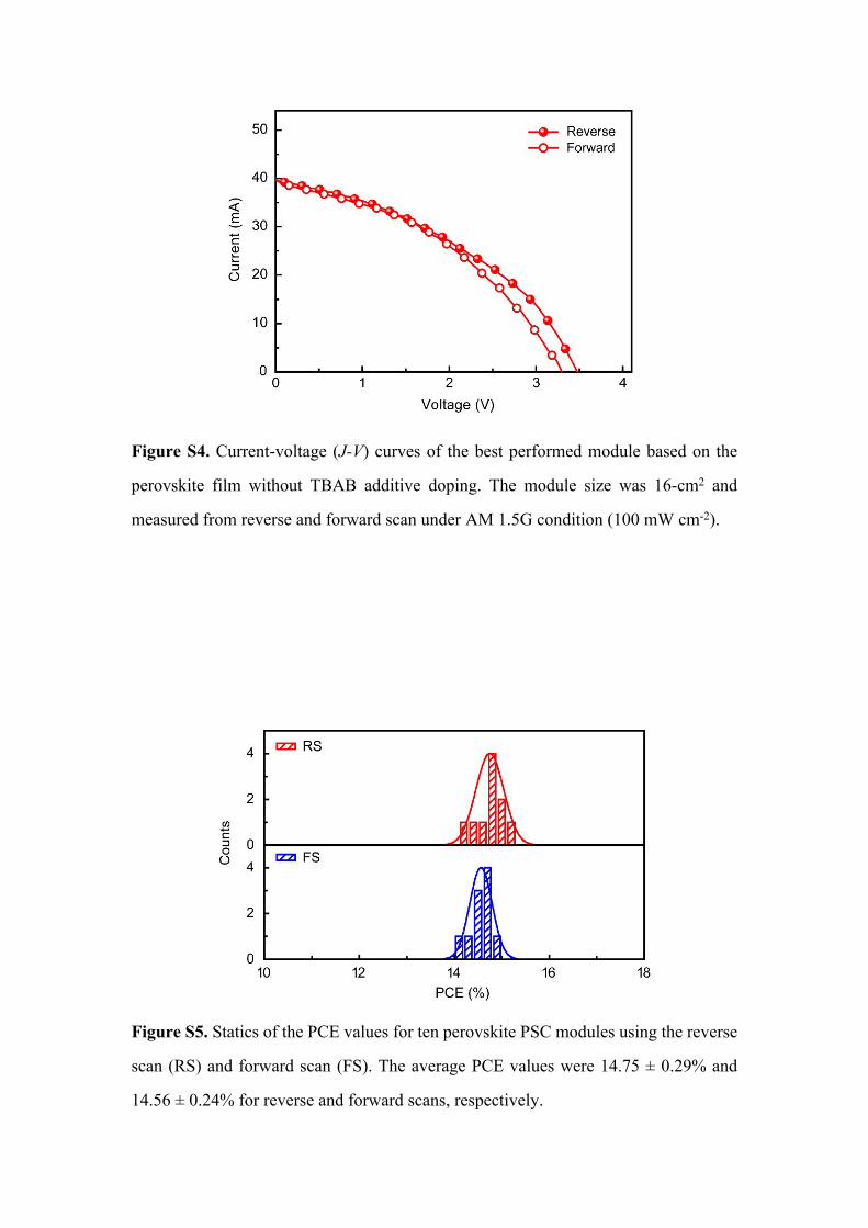
Figure S4. Current-voltage (J-V) curves of the best performed module based on the
perovskite film without TBAB additive doping. The module size was 16-cm2 and
measured from reverse and forward scan under AM 1.5G condition (100 mW cm-2).
Figure S5. Statics of the PCE values for ten perovskite PSC modules using the reverse
scan (RS) and forward scan (FS). The average PCE values were 14.75 ± 0.29% and
14.56 ± 0.24% for reverse and forward scans, respectively.
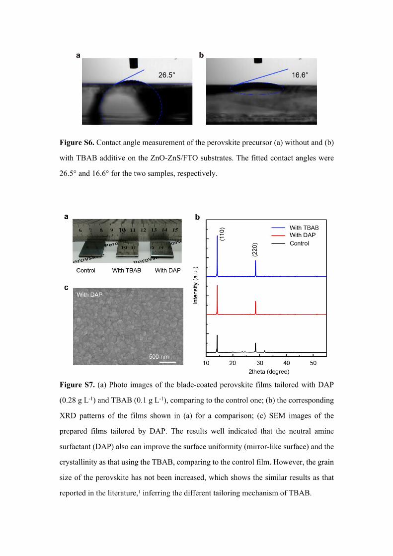
Figure S6. Contact angle measurement of the perovskite precursor (a) without and (b)
with TBAB additive on the ZnO-ZnS/FTO substrates. The fitted contact angles were
26.5° and 16.6° for the two samples, respectively.
Figure S7. (a) Photo images of the blade-coated perovskite films tailored with DAP
(0.28 g L-1) and TBAB (0.1 g L-1), comparing to the control one; (b) the corresponding
XRD patterns of the films shown in (a) for a comparison; (c) SEM images of the
prepared films tailored by DAP. The results well indicated that the neutral amine
surfactant (DAP) also can improve the surface uniformity (mirror-like surface) and the
crystallinity as that using the TBAB, comparing to the control film. However, the grain
size of the perovskite has not been increased, which shows the similar results as that
reported in the literature,1 inferring the different tailoring mechanism of TBAB.
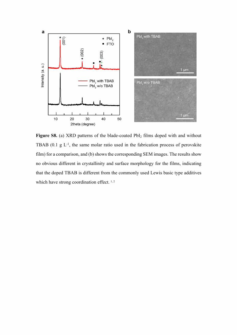
Figure S8. (a) XRD patterns of the blade-coated PbI2 films doped with and without
TBAB (0.1 g L-1, the same molar ratio used in the fabrication process of perovskite
film) for a comparison, and (b) shows the corresponding SEM images. The results show
no obvious different in crystallinity and surface morphology for the films, indicating
that the doped TBAB is different from the commonly used Lewis basic type additives
which have strong coordination effect. 1, 2

Figure S9. IPCE spectra and integrated current density Jsc for the best-performing cells
in Figure 4a, which were fabricated using the perovskite films tailored with or without
TBAB. The integrated Jsc for the cells with and without TBAB doping was 22.45 mA
cm-2 and 20.87 mA cm-2, respectively, which matched well with the J-V measurement.
Figure S10. Color evolution of the perovskite films aging in open air under the high
RH about 85%. The much slower color changing from black to yellow due to the
moisture induced decomposition indicates the obviously increased moisture stability
for the TBAB doped film with comparison to the control one.
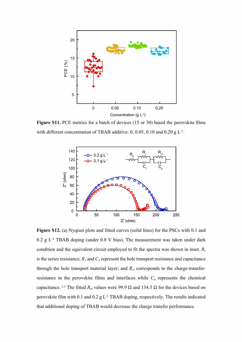
Figure S11. PCE metrics for a batch of devices (15 or 30) based the perovskite films
with different concentration of TBAB additive: 0, 0.05, 0.10 and 0.20 g L-1.
Figure S12. (a) Nyqiust plots and fitted curves (solid lines) for the PSCs with 0.1 and
0.2 g L-1 TBAB doping (under 0.8 V bias). The measurement was taken under dark
condition and the equivalent circuit employed to fit the spectra was shown in inset. Rs
is the series resistance; R1 and C1 represent the hole transport resistance and capacitance
through the hole transport material layer; and Rct corresponds to the charge-transfer-
resistance in the perovskite films and interfaces while Cμ represents the chemical
capacitance. 3-5 The fitted Rct values were 99.9 Ω and 134.5 Ω for the devices based on
perovskite film with 0.1 and 0.2 g L-1 TBAB doping, respectively. The results indicated
that additional doping of TBAB would decrease the charge transfer performance.

Figure S13. Photo images of perovskite films based on the precursor without additive
doping or doped with SDS, TBAC and TBAB, respectively.
References:1. W. Q. Wu, Z. Yang, P. N. Rudd, Y. Shao, X. Dai, H. Wei, J. Zhao, Y. Fang, Q. Wang, Y. Liu, Y.
Deng, X. Xiao, Y. Feng and J. Huang, Sci Adv, 2019, 5, eaav8925.2. J.-W. Lee, Z. Dai, C. Lee, H. M. Lee, T.-H. Han, N. De Marco, O. Lin, C. S. Choi, B. Dunn, J.
Koh, D. Di Carlo, J. H. Ko, H. D. Maynard and Y. Yang, J. Am. Chem. Soc., 2018, 140, 6317-6324.
3. H. S. Kim, I. Mora-Sero, V. Gonzalez-Pedro, F. Fabregat-Santiago, E. J. Juarez-Perez, N. G. Park and J. Bisquert, Nature Commun., 2013, 4, 2242.
4. H. S. Kim, J. W. Lee, N. Yantara, P. P. Boix, S. A. Kulkarni, S. Mhaisalkar, M. Gratzel and N. G. Park, Nano Lett., 2013, 13, 2412-2417.
5. J. Bisquert, J. Phys. Chem. B, 2002, 106, 325-333.