bits to antenna and back - richardson rfpd
TRANSCRIPT

The World Leader in High Performance Signal Processing Solutions
June 2012
Larry Hawkins
Bits to Antenna and Back

ADL5324 400 – 4000 MHz Broadband ½ W RF Driver Amplifier
FEATURES 3.3 V to 5 V Dynamically adjustable bias
-40°C to 105°C operating temperature range Minimal external matching components Temperature and frequency stability
KEY SPECIFICATIONS (5 V) Frequency range: 400 - 4000 MHz
Gain: 14.6 dB @ 2140 MHz P1dB: 29.1 dBm @ 2140 MHz OIP3: 43.1 dBm @ 2140 MHz
Noise figure: 3.8 dB @ 2140 MHz Power supply: 3.3 V – 5 V
Low quiescent current: 62 mA – 133 mA Package: SOT-89
ESD rating: ±3 kV (Class 2)


FEATURES Sub-1Hz frequency resolution (25bit
Modulus) High and low speed FMCW ramps (~20us) FSK and PSK modulation capability Less than 100mW power consumption Generates highly linear saw tooth and
triangular waveforms Ramp modes: Parabolic, superimposed
with FSK, 2 different sweep rates, delay, frequency read back, interruption
Cycle slip reduction for fast lock times 24-LFCSP (4mm x 4mm)
KEY SPECIFICATIONS 500MHz – 13GHz range 25 bit divider modulus 110MHz PFD maximum frequency Normalised PN Floor = -222dBc/Hz FSK modulation Current = 33mA @ 3V
ADF4159: Direct Modulation/Waveform Generating
13GHz Fractional-N Frequency Synthesizer
LOCKDETECT
N COUNTER
CP
REFERENCE
DATALE
32-BITDATA
REGISTER
CLK
REFIN
AVDD
AGND
VDD
VDD
DGND
RDIV
SDOUT
NDIV
DGND CPGND
DVDD VP
CE
RSET
RFINA
RFINB
OUTPUTMUX
MUXOUT
–
+
HIGH Z
PHASEFREQUENCYDETECTOR
ADF4159
THIRD-ORDERFRACTIONAL
INTERPOLATOR
MODULUS225
FRACTIONREG
INTEGERREG
×2DOUBLER
5-BITR COUNTER
CHARGEPUMP
CSR
÷2DIVIDER
SW1
SW2
TXDATA
FLO SWITCH

ADF4159– What is it?
The ADF4159 is a 13GHz fractional-N frequency synthesizer with modulation and waveform generation capability.
Features 25-bit fixed modulus, allowing sub-hertz resolution at 13GHz. Max PFD=110MHz It consists of a low noise digital phase frequency detector (PFD), a
precision charge pump, and a programmable reference divider. Programmable fractional-N division The INT and FRAC registers define an overall N divider N = INT +
(FRAC/225). Implement FSK, PSK modulation.
High and low speed FMCW ramps generation Digital programmable frequency sweep modes available Saw-tooth and triangular waveforms.
ADF4159 cycle slip reduction circuitry which leads to faster lock times Digital Lock Detect Control of all on-chip registers is via a simple 3-wire interface. Analog power supply ranging from 2.7 V to 3.3 V. (33mA @ 3V) Digital Power Supply 1.8V

AD9914/5 Very High Speed, High Performance DDS
High SpeedDDS core
Ref ClockInput Circuitry
User interface
Timing andControl
12 Bit DACDigitalSineWave
AD9914: 3.5(+/-) GSPS* AD9915: 2.5 GSPS
KEY BENEFITS & FEATURES Designed for performance Pin access to tuning words
32 bits Access FTW, POW & ASF, or Aux TW
Sweep any parameter Programmable Modulus multi-chip synchronization 8 profile registers 2.5 GHz REFCLK PLL ~2.5W total power Process: 0.18um SiGe Package: 88 lead LFCSP
*4.0 GHz should be attainable with degradation to some specs

Date: 11.MAR.2011 13:18:18
AD9914: Fs=3.2Gsps, Fo=1.47GHz SFDR~ -56dbc

Residual phase noise

The World Leader in High Performance Signal Processing Solutions
Circuits from the Lab™ Reference Circuits

Circuits from the Lab™ What is a Circuit from the Lab?
Engineered by ADI experts for tough RF design challenges Tested to ensure reliable, low-risk implementation Ready to integrate using provided design files and hardware
Circuits can be found on individual product pages;
by viewing the complete library on analog.com: www.analog.com/circuits or on RichardsonRFPD.com: http://apps.richardsonrfpd.com/Mktg/ADI-CftLs.html

Circuits from the Lab™ Anatomy 101
Commercially Available Circuit Evaluation Hardware (not available for all circuits)
Design & Integration Files Circuit Note
• Value Proposition • Theory of Operation • Design Guidance • Test Data • Circuit Evaluation and Test • Common Variations
• Schematics • Gerbers/NC Drill • Bill of Materials • Layout Files • Linux Device Driver (when applicable)

CN0243 High Dynamic Range Direct Conversion Transmitter with Single External Reference
Broadband DAC-IQ Mod Interface Circuit
LO range from 750 MHz to 2.9 GHz
Clock synth., distribution function generates DAC sample clock and IQMod LO from single reference
Dedicated hardware pcb available (CFTL-CN0243-EVALZ)
More information at: www.analog.com/CN0243

FEATURES LO range
750 – 1100 MHz (ADRF6701) 1550 – 2150 MHz (ADRF6702) 2100 – 2600 MHz (ADRF6703) 2500 – 2900 MHz (ADRF6704)
Matched 50 ohm output Integrated VCO & PLL + ext LO option Programmable VCO band 40-Lead LFCSP (6mm x 6mm)
KEY SPECIFICATIONS (2GHz) Modulator OIP3: +30dBm Modulator OP1dB: +15dBm Modulator noise: -158dBm/Hz Carrier leakage: <-40dBm Sideband suppression: <-45dBc Output ACP: -70dBc Pout: -7dBm
ADRF6701/2/3/4 I/Q Modulator, PLL & VCO Family

The World Leader in High Performance Signal Processing Solutions
Analog Devices JESD204 ADC Interfaces

Why JESD204? Simplification of overall system design Smaller/lower number of trace routes, easier to route board designs
Reduction in pin count – Both the Tx and Rx side Move from high pin count low speed parallel interfaces to low pin
count high speed serial interfaces Embedded clock incorporated to even further reduce pin count
Reduction in system costs Smaller IC packages and board designs lead to lower cost
Easily scalable to meet future bandwidth requirements As geometries shrink and speed increases, the standard adapts
FPGA/ASICA/D Converter FPGA/ASICA/D Converter

JESD204 Evolution
JESD204 (April 2006) defined the translation of
samples across a single serial lane for multiple converters at speeds up to 3.125 Gbps
JESD204A (April 2008) added capability for multiple
aligned serial lanes with multiple converters at speeds up to 3.125 Gbps
JESD204 Evolution
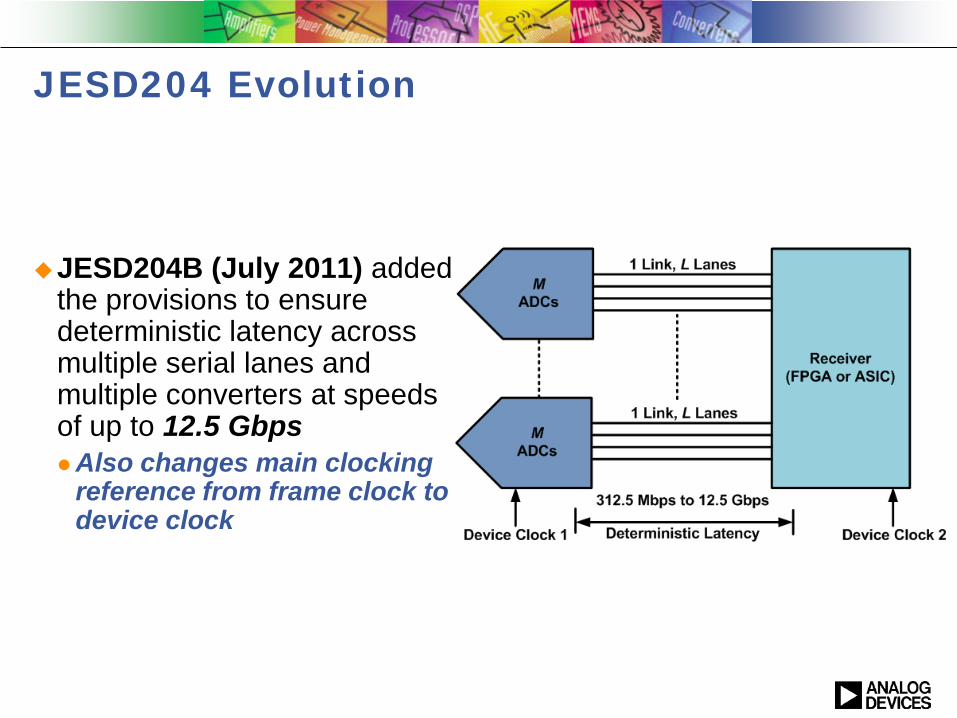
JESD204B (July 2011) added the provisions to ensure deterministic latency across multiple serial lanes and multiple converters at speeds of up to 12.5 Gbps Also changes main clocking
reference from frame clock to device clock

Analog Devices JESD204/A Product Offerings
AD9639 Quad 12-bit 170/210 MSPS ADC offering JESD204 SNR = 65 dBFS, SFDR = 77 dBc
AD9644 Dual 14-bit 80/155 MSPS ADC offering JESD204A SNR = 73.7 dBFS, SFDR = 92 dBc
AD9641 Single 14-bit 80/155 MSPS ADC offering JESD204A SNR = 73.7 dBFS, SFDR = 94 dBc

AD9128 Dual TxDAC+® with JESD204A Serial Interface KEY FEATURES 16-bit dual DAC 1.25 GSPS DAC Update Rate 4 Lanes of high-speed JESD204A serial links (each capable of 3.125 Gbps) Selectable 2X/4X/8X half-band interpolation filters 32-bit NCO for carrier placement flexibility Channel matching control for optimal LO/SSB cancellation Multiple chip synchronization interface Configurable clock multiplier/divider Digital inverse sinc filter APPLICATIONS Wireless infrastructure: Supports multiple telecommunications standards
including: GSM, WCDMA, TD-SCDMA, CDMA2000, WiMAX, and LTE Wideband communications: LMDS/MMDS & point-to-point