be lab manual 2014 iit bhubaneswar
TRANSCRIPT

BBASI
INDIAN IN
SA
IC EL
Lab
SCHOOL OF
NSTITUTE O
AMATAPUR
LECT
b Man
F ELECTRICA
F TECHNOLO
RI, ODISHA‐7
TRO
nual
AL SCIENCES
OGY, BHUBA
751013, INDI
ONIC
ANESWAR
IA
CS

i. Title
ii. Con
iii. Co
iv. Po
v. Lab
vi. Un
vii. Li
IND
e page
ntents
ourse Outline
oints For Ma
boratory Equ
ndertaking
ist of Experim
DIANINSTSCH
e
intaining La
uipment Issu
ments
TITUTEOHOOLOFE
C
b Records
ue Slip
FTECHNOELECTRIC
Content
OLGYBHUALSCIENC
ts
UBANESWCES
WAR
Page No.
1
2
3
4
5
6
7
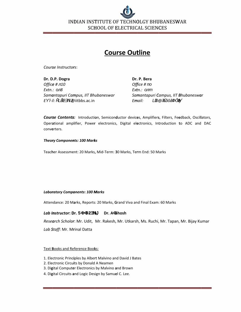
Cours
Dr. D.P. DograOfficeExtn.SamaEƳŀ
Cours
Opera
conve
Theor
Teach
Labor
Atten
Lab In
Resea
Lab S
Text B
1. Ele2. Ele3. Dig
4. Dig
IND
se Instructor
e # л10 : ол8 antapuri Camil: ŘLJŘƻƎNJŀ@iitbbs.ac.in
se Contents
ational ampl
erters.
ry Componen
her Assessme
ratory Compo
dance: 20 Ma
nstructor: D
arch Scholar
Staff: Mr. Mr
Books and Re
ctronic Princictronic Circuigital Compute
gital Circuits a
DIANINSTSCH
rs:
mpus, IIT Bh
s: Introductio
lifier, Power
nts: 100 Mark
nt: 20 Marks,
onents: 100 M
arks, Reports
Dr. 5ΦtΦ5ƻƎNJŀ
r: Mr. Udit,
rinal Datta
ference Book
iples by Alberits by Donald er Electronics
and Logic Des
TITUTEOHOOLOFE
Cou
ubaneswar
on, Semicond
r electronics
ks
, Mid‐Term: 3
Marks
: 20 Marks, G
a, Dr. AΦ
Mr. Rakesh, Mr. Utkarsh, Ms. Ruchi, Mr. Tapan, Mr. Bijay Kumar
ks:
rt Malvino anA Neamen by Malvino a
ign by Samue
FTECHNOELECTRIC
rse Out
Dr.OffExtSamEm
ductor device
, Digital ele
30 Marks, Ter
Grand Viva an
Ghosh
.
d David J Bat
and Brown
el C. Lee.
OLGYBHUALSCIENC
tline
P. Berafice # по tn.: олт mantapuri Cmail: LJƭō ƛƛǘōōǎΦŀŎΦƛƴ
es, Amplifiers
ectronics, Int
rm End: 50 M
d Final Exam
es
UBANESWCES
Campus, IIT B@
s, Filters, Fee
troduction t
arks
: 60 Marks
WAR
Bhubaneswa
edback, Oscill
to ADC and
ar
lators,
DAC

1
2
3
4
5
6
7
8
9
1
IND
P
. Maintain
. Draw the
. Write theCompone
. Use Pro‐c
. Note dow
. Name diffa) A.b) D.
. Graph and
. Don’t frac
. Resistor &should be
0. All the ca
DIANINSTSCH
Points F
the content
circuit diagr
e specificatioent etc.) prop
circle for dra
wn the range
ferent suppC supply shoC supply sho
d Tracing sh
ction (whene
& Inductor se clear).
lculation pa
TITUTEOHOOLOFE
For Mai
ts properly g
ram clearly u
on of instrumperly.
wing all met
e & type of m
ply & their raould be cleaould be clea
ould be past
ever not req
should be d
rt should be
FTECHNOELECTRIC
intainin
giving experi
using HB pen
ment (such a
ters.
meters used
ange clearly rly indicatedrly indicated
ted at left gu
quired) the A
rawn prope
on left side
OLGYBHUALSCIENC
ng Lab R
ment date &
ncil.
as CRO, Sign
in circuit dia
as mentioned by Phase &d with polari
utter positio
Axis when yo
rly. (i.e. Insi
(plane side)
UBANESWCES
Records
& submission
nal Generato
agram.
ed below‐ & Neutral witity (+ & ‐).
on.
ou draw the
ide two invi
) of record.
WAR
s
n date clearl
or, Power Su
th frequency
graph.
sible paralle
ly.
upply,
y.
el line
L
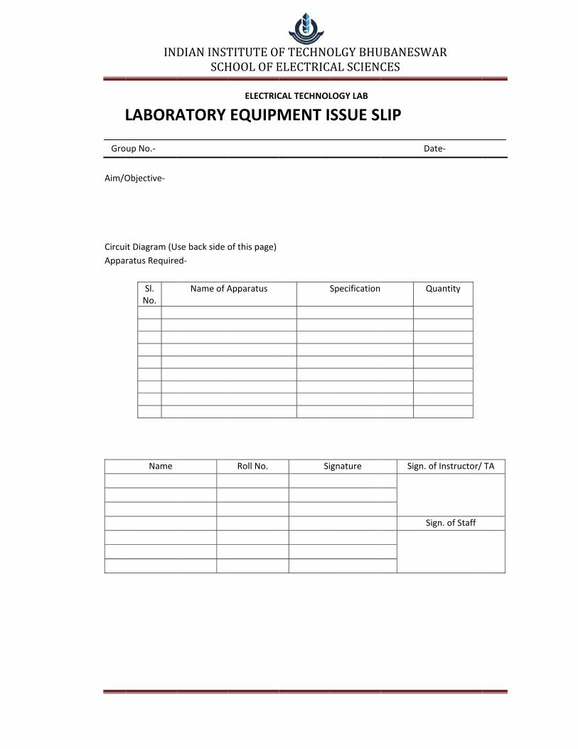
Gro
Aim/O
Circui
Appar
IND
LABORA
up No.‐
Objective‐
it Diagram (U
ratus Require
Sl. No.
Name
DIANINSTSCH
ATORY
se back side o
ed‐
Name of A
TITUTEOHOOLOFE
ELECTRIC
EQUIPM
of this page)
Apparatus
Roll No.
FTECHNOELECTRIC
CAL TECHNOL
MENT I
Si
OLGYBHUALSCIENC
LOGY LAB
SSUE S
Specification
ignature
UBANESWCES
LIP
Da
Q
Sign. o
Si
WAR
ate‐
Quantity
of Instructor/
ign. of Staff
TA

I ha
the
and
that
imm
actio
Stud
Nam
Roll
IND
ave read
BASIC EL
procedu
t failure
mediate d
on may b
dent’s Sig
me‐
No‐
DIANINSTSCH
and unde
ECTRONI
ures at all
to follow
dismissal
be taken a
gnature
TITUTEOHOOLOFE
Un
erstand t
CS LABOR
l times w
w these r
from the
according
FTECHNOELECTRIC
ndertak
the rules
RATORY.
while using
rules and
e laborato
g to the In
OLGYBHUALSCIENC
ing
and pro
I agree to
g these f
procedu
ory and a
nstitute p
Dat
UBANESWCES
ocedures
o abide b
facilities.
ures will
additiona
policies.
te‐
WAR
set forth
by these r
I underst
result in
al disciplin
h for
rules
tand
my
nary
0
1
2
3
4
5
6
7
8
9
1
IND
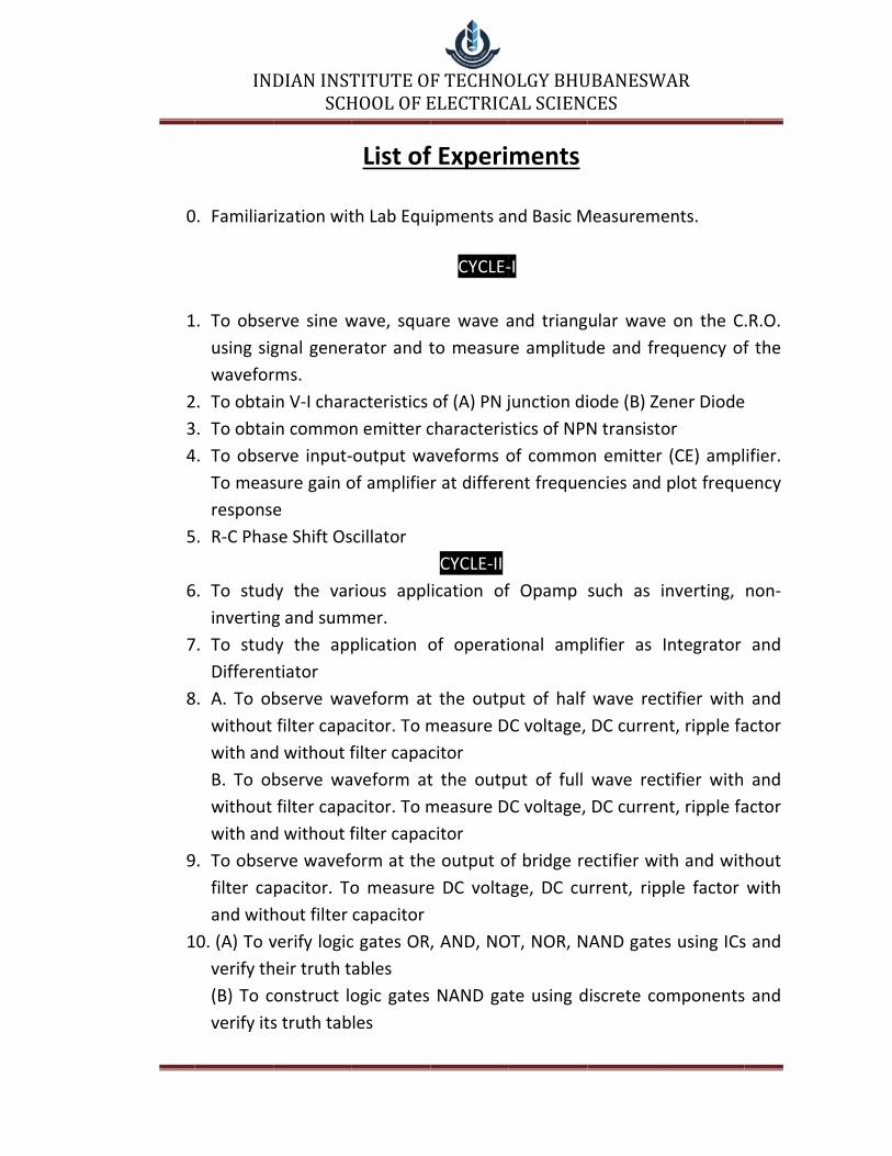
0. Familiar
. To obse
using sig
wavefor
. To obtai
. To obtai
4. To obse
To meas
response
. R‐C Phas
6. To stud
inverting
7. To stud
Differen
8. A. To ob
without
with and
B. To ob
without
with and
. To obse
filter ca
and with
0. (A) To v
verify th
(B) To c
verify its
DIANINSTSCH
ization wit
erve sine w
gnal gener
rms.
in V‐I chara
in common
rve input‐
sure gain o
e
se Shift Os
y the var
g and sum
y the app
tiator
bserve wa
filter capa
d without f
bserve wa
filter capa
d without f
rve wavefo
pacitor. To
hout filter
verify logic
heir truth t
onstruct lo
s truth tab
TITUTEOHOOLOFE
List of
th Lab Equ
wave, squa
rator and t
acteristics
n emitter c
output wa
of amplifie
cillator
rious appl
mer.
plication o
veform at
acitor. To m
filter capac
aveform at
acitor. To m
filter capac
orm at the
o measure
capacitor
c gates OR,
ables
ogic gates
les
FTECHNOELECTRIC
f Experi
ipments an
CYCLE‐
are wave a
to measur
of (A) PN j
characteris
aveforms o
r at differe
CYCLE‐II
ication of
of operati
t the outp
measure D
citor
t the outp
measure D
citor
e output o
e DC volta
, AND, NO
NAND ga
OLGYBHUALSCIENC
ments
nd Basic M
‐I
and triang
re amplitud
junction di
stics of NPN
of commo
ent freque
f Opamp
ional amp
ut of half
C voltage,
put of full
C voltage,
of bridge re
ge, DC cu
OT, NOR, N
te using d
UBANESWCES
Measureme
ular wave
de and fre
iode (B) Ze
N transisto
n emitter
ncies and
such as i
plifier as I
wave rect
DC curren
wave rect
DC curren
ectifier wit
rrent, ripp
AND gates
iscrete co
WAR
ents.
on the C
equency of
ener Diode
or
(CE) ampl
plot frequ
nverting,
ntegrator
tifier with
nt, ripple fa
tifier with
nt, ripple fa
th and wit
ple factor
s using ICs
mponents
.R.O.
f the
ifier.
ency
non‐
and
and
actor
and
actor
hout
with
s and
and
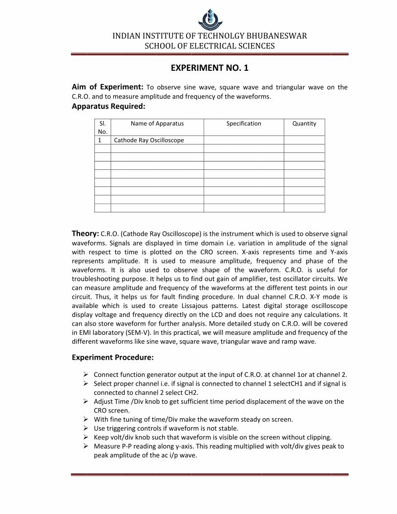
Aim C.R.O
Appa
Theowavewith reprewavetroubcan mcircuiavailadisplacan ain EMdiffer
Expe
IND
of ExperiO. and to me
aratus Req
Sl. No.
1 Cat
ory: C.R.O. (eforms. Signrespect to
esents ampleforms. It isbleshooting measure amit. Thus, it able which ay voltage aalso store waMI laboratoryrent wavefo
eriment Pr
Connect f Select pro
connecte Adjust Tim
CRO scree With fine Use trigge Keep volt Measure
peak amp
DIANINSTSCH
iment: To easure ampli
quired:
Name of A
thode Ray Os
(Cathode Ra
als are disptime is plolitude. It iss also usedpurpose. It plitude and helps us foris used to
and frequencaveform for y (SEM‐V). Inrms like sine
rocedure:
function genoper channed to channeme /Div knoben. tuning of timering contro/div knob suP‐P reading plitude of the
TITUTEOHOOLOFE
EXPE
observe sin
tude and fre
Apparatus
scilloscope
y Oscillosco
played in timotted on ths used to md to observhelps us to ffrequency or fault findicreate Lisscy directly ofurther anan this practice wave, squa
nerator outpel i.e. if signal 2 select CHb to get suff
me/Div makls if waveforuch that wavalong y‐axise ac i/p wav
FTECHNOELECTRIC
RIMENT
ne wave, sq
equency of t
pe) is the in
me domain he CRO scremeasure amve shape ofind out gainof the waveng procedusajous patteon the LCD aalysis. More cal, we will mare wave, tri
put at the inpal is connecteH2. ficient time p
ke the wavefrm is not staveform is viss. This readine.
OLGYBHUALSCIENC
NO. 1
uare wave
the waveform
Specification
strument wh
i.e. variationeen. X‐axis mplitude, freof the waven of amplifieeforms at there. In dual erns. Latest and does nodetailed stumeasure amiangular wav
put of C.R.O.ed to channe
period displa
form steady able. sible on the sng multiplied
UBANESWCES
and triangu
ms.
Q
hich is used
n in ampliturepresents equency aneform. C.R.er, test oscile different tchannel C.Rdigital stor
ot require anudy on C.R.Omplitude and ve and ramp
. at channel el 1 selectCH
acement of t
on screen.
screen withod with volt/d
WAR
ular wave o
Quantity
to observe s
ude of the stime and Y
nd phase oO. is usefulator circuitstest points iR.O. X‐Y morage oscillosny calculatioO. will be covfrequency o
p wave.
1or at chanH1 and if sig
the wave on
out clipping.div gives pea
n the
signal
signal Y‐axis f the ul for s. We n our ode is scope ons. It vered of the
nel 2. nal is
n the
ak to
Draw
Obse
Funct
Sine W
SquaWave
TrianWave
Conc
IND
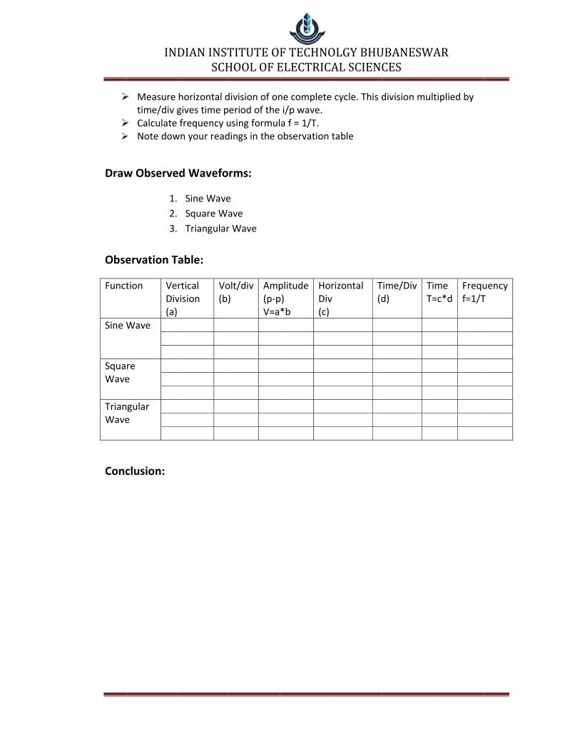
Measure time/div g
Calculate Note dow
w Observe
1.
2.
3.
ervation T
tion VeDiv(a)
Wave
re e
gular e
clusion:
DIANINSTSCH
horizontal dgives time pfrequency u
wn your read
ed Wavefo
Sine Wave
Square Wa
Triangular
able:
rtical vision
Vo(b)
TITUTEOHOOLOFE
division of oneriod of theusing formuldings in the o
rms:
e
ave
r Wave
olt/div)
Amp(p‐pV=a
FTECHNOELECTRIC
ne complete i/p wave. a f = 1/T. observation
plitudep) *b
HoDiv(c)
OLGYBHUALSCIENC
e cycle. This d
table
rizontal v
T(d
UBANESWCES
division mul
Time/Div d)
TiT=
WAR
tiplied by
ime =c*d
Frequf=1/T
uencyT

Aim
Appa
Theotype show
At thchargchargelectchargside idista
Wor
Whenfigurecatho
IND
of Experim
aratus Req
Sl. No.
ory: The semof impurity
wn in the foll
he junction iged ions in Pged ion) andron and becge carrier is is preventednce by deple
rking princ
n voltage is e. When theode) two pos
DIANINSTSCH
ment: To ob
quired:
Name of A
miconducto
y in anotherowing figure
initially freeP side of junc positively ccomes positicalled as d
d because ofetion (acts a
iple:
not applied e voltage is ssibilities ari
TITUTEOHOOLOFE
EXPERI
btain V‐I cha
Apparatus
r diode is fo
r side of thee.
e charge carction(an atocharged ion oively chargedepletion regf the depletis a sort of in
across the d applied beises depend
FTECHNOELECTRIC
MENT NO
aracteristics
ormed by do
e semicond
rriers from bom in P‐side on n side(and ion)regiongion. Furtheion voltage gnsulation) lay
diode, depletween the ting on polar
OLGYBHUALSCIENC
O. 2 (A)
of PN juncti
Specification
oping P‐type
uctor crysta
both side reaccept electn atom in n‐sn. This regionr recombinagenerated dyer as show
etion region two terminaity of DC sup
UBANESWCES
on diode
Q
e impurity in
al forming a
ecombine fotron and becside accepts n deplete ofation of freedue to chargn dotted in t
forms as shoals of the dpply.
WAR
Quantity
n one side a
a p‐n junctio
orming negacomes negahole i.e. dof any type oe carrier on e carriers kethe above fig
own in the aiode (anode
nd N‐
on as
tively tively nates f free both
ept at gure.
above e and
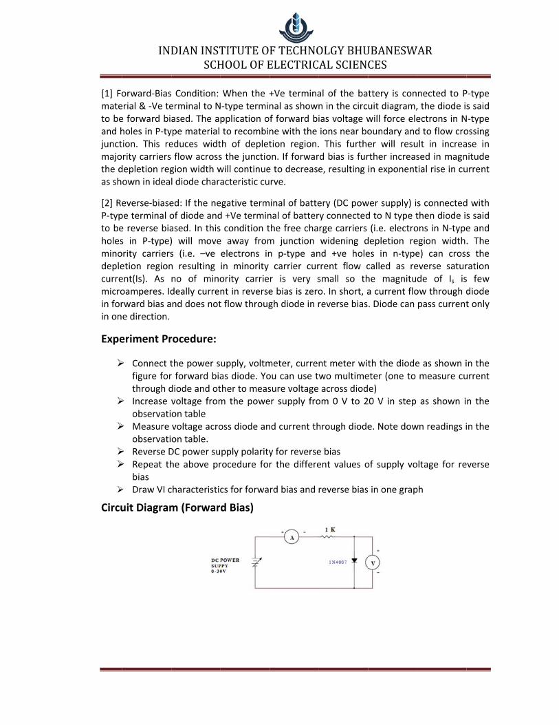
[1] Fomateto beand hjunctmajothe das sh
[2] ReP‐typto beholesminodeplecurremicroin forin on
Expe
Circu
IND
orward‐Biaserial & ‐Ve tee forward biholes in P‐tyion. This rerity carriers depletion regown in idea
everse‐biasepe terminal oe reverse bias in P‐type)ority carriersetion regionent(Is). As oamperes. Idrward bias ae direction.
eriment Pr
Connect tfigure forthrough d
Increase vobservati
Measure observati
Reverse D Repeat th
bias Draw VI c
uit Diagram
DIANINSTSCH
Condition: erminal to Nased. The apype material educes widtflow acrossgion width wl diode chara
ed: If the neof diode andased. In this) will moves (i.e. –ve n resulting no of minodeally currennd does not
rocedure:
the power sr forward biadiode and otvoltage fromon table voltage acroon table. DC power suhe above pr
characteristic
m (Forwar
TITUTEOHOOLOFE
When the +N‐type terminpplication oto recombinth of deplets the junctiowill continueacteristic cu
egative termd +Ve termin condition te away fromelectrons inin minority ority carrient in reverset flow throug
upply, voltmas diode. Yother to measm the powe
oss diode an
pply polarityrocedure for
cs for forwa
d Bias)
FTECHNOELECTRIC
+Ve terminanal as shownf forward bine with the tion region.on. If forware to decreaserve.
inal of battenal of batterthe free cham junction n p‐type ancarrier curr is very se bias is zerogh diode in r
meter, currenou can use twsure voltage er supply fro
nd current th
y for reverser the differe
rd bias and r
OLGYBHUALSCIENC
al of the ban in the circias voltage wions near bo This furtherd bias is fure, resulting
ery (DC powry connectedrge carriers widening dnd +ve holerrent flow csmall so tho. In short, areverse bias
nt meter witwo multimeacross diod
om 0 V to 2
hrough diode
e bias ent values o
reverse bias
UBANESWCES
ttery is conuit diagram,will force eleoundary ander will resurther increasin exponent
wer supply) isd to N type t(i.e. electro
depletion rees in n‐typecalled as rehe magnituda current flo. Diode can
th the diodeeter (one to e) 20 V in step
e. Note dow
of supply vo
in one grap
WAR
nected to P, the diode isectrons in Nd to flow croult in increased in magntial rise in cu
s connectedthen diode isons in N‐typeegion widthe) can crosseverse saturde of Is isow through dpass current
e as shown imeasure cu
as shown i
wn readings i
ltage for re
ph
P‐type s said N‐type ossing ase in nitude urrent
d with s said e and . The s the ration s few diode t only
in the urrent
n the
in the
verse

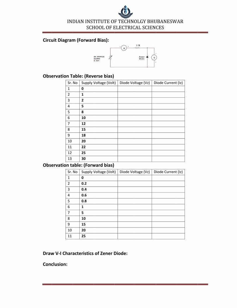
Circu
Obse
Obse
Draw
Conc
IND
uit Diagram
ervation T
Sr. No
1
2
3
4
5
6
7
8
9
10
11
12
13
ervation ta
Sr. N
1
2
3
4
5
6
7
8
w V‐I Chara
clusion:
DIANINSTSCH
m (Reverse
able: (Forw
o Supply Vo
0
0.2
0.4
0.6
0.8
1
2
4
6
8
10
15
20
able: (Reve
No Supply V
0
2
5
10
15
20
25
30
acteristics
TITUTEOHOOLOFE
e Bias):
ward bias)
oltage (Volt)
erse bias)
Voltage (Volt)
of PN Jun
FTECHNOELECTRIC
)
Diode Vol
) Diode Vol
nction Diod
OLGYBHUALSCIENC
ltage (Vd)
tage (Vd) D
de:
UBANESWCES
Diode Curre
Diode Current
WAR
ent (Id)
t (Id)

Aim
Appa
Theois usbreakamoudiodecurreForw
Expe
Circu
IND
of Experim
aratus Req
Sl. No.
ory: The Zeed for voltkdown voltaunt of dopine. If power ent is 0.1A oard characte
eriment Pr
Connect tfigure for diode and
Increase observati
Measure observati
Reverse D Repeat th
bias Draw VI c
uit Diagram
DIANINSTSCH
ment: To ob
quired:
Name of A
ner diode is
age regulatage called Zng. Breakdowcapacity ofr 100 mA. Iferistics of th
rocedure:
the power s reverse biad other to mvoltage fromon table voltage acroon table. DC power suhe above pr
characteristic
m (Reverse
TITUTEOHOOLOFE
EXPERI
btain V‐I cha
Apparatus
designed to
ion purposeZener breakwn current if the Zener f current ince Zener diod
upply, voltms. You can u
measure voltam the powe
oss diode an
pply polarityrocedure for
cs for revers
e Bias)
FTECHNOELECTRIC
MENT NO
aracteristics
o operate in
e. Zener diokdown voltas limited byis 1 W andcreases morede is similar
meter, currense two multage across der supply fro
nd current th
y for forwardr the differe
se bias and f
OLGYBHUALSCIENC
O. 2 (B)
of Zener dio
Specification
reverse bre
odes are deage (Vz). Thy power dissd Zener volte than this lto normal P
nt meter wittimeter (oneiode) om 0V to 2
hrough diode
d bias ent values o
forward bias
UBANESWCES
ode
Q
eakdown reg
esigned for he value ofipation capatage is 10V,imit, diode PN junction d
th the diodee to measure
20V in step
e. Note dow
of supply vo
in one grap
WAR
Quantity
gion. Zener d
specific ref Vz dependacity of the , highest rewill be damdiode.
e as shown ie current thr
as shown i
wn readings i
ltage for re
ph
diode
verse ds on zener verse aged.
in the rough
n the
in the
verse
Circu
Obse
Obse
Draw
Conc
IND
uit Diagram
ervation TSr.
1
2
3
4
5
6
7
8
9
10
11
12
13
ervation taSr.
1
2
3
4
5
6
7
8
9
10
11
w V‐I Chara
clusion:
DIANINSTSCH
m (Forwar
able: (RevNo Supply V
0
1
2
5
8
10
12
15
18
20
22
25
30
able: (ForwNo Supply V
0
0.2
0.4
0.6
0.8
1
5
10
15
20
25
acteristics
TITUTEOHOOLOFE
d Bias):
verse bias)Voltage (Volt
ward bias)Voltage (Volt
of Zener D
FTECHNOELECTRIC
t) Diode Vol
t) Diode Vol
Diode:
OLGYBHUALSCIENC
ltage (Vz) D
ltage (Vz) D
UBANESWCES
Diode Current
Diode Current
WAR
(Iz)
(Iz)
Aim
Appa
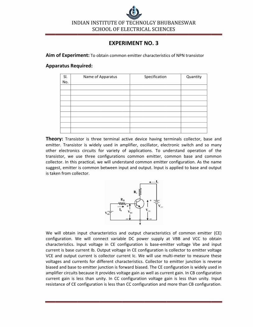
Theoemittothertranscollecsuggeis tak
We wconfigcharacurreVCE avoltabiaseamplcurreresist
IND
of Experim
aratus Req
Sl. No.
ory: Transister. Transistr electronicsistor, we uctor. In this est, emitter ken from col
will obtain guration. Wacteristics. Ient is base cand output ges and cured and base ifier circuits ent gain is ltance of CE c
DIANINSTSCH
ment: To ob
quired:
Name of A
stor is three
tor is widelycs circuits fuse three cpractical, wis common lector.
input charaWe will connput voltagurrent Ib. Ocurrent is crrents for dito emitter jubecause it pess than unconfiguratio
TITUTEOHOOLOFE
EXPE
btain commo
Apparatus
e terminal a
y used in afor variety onfiguration
we will undebetween in
cteristics annect variabge in CE coutput voltagcollector curifferent chaunction is foprovides volnity. In CC con is less tha
FTECHNOELECTRIC
RIMENT
on emitter c
active devic
mplifier, osof applicatins common rstand commput and out
nd output cble DC pownfiguration ge in CE conrrent Ic. Weracteristics. orward biasetage gain asconfiguratioan CC configu
OLGYBHUALSCIENC
NO. 3
characteristic
Specification
ce having te
cillator, elecions. To unemitter, c
mon emittertput. Input is
characteristiwer supply ais base‐emi
nfiguration ise will use mCollector to
ed. The CE cos well as currn voltage guration and
UBANESWCES
cs of NPN tr
Q
erminals col
ctronic switnderstand oommon basr configurats applied to
cs of commat VBB anditter voltages collector toulti‐meter to emitter juonfigurationrent gain. In ain is less tmore than C
WAR
ansistor
Quantity
llector, base
tch and so operation ose and comion. As the base and o
mon emitterd VCC to oe Vbe and o emitter voo measure tnction is re is widely usCB configurthan unity. CB configura
e and
many f the mmon name utput
r (CE) obtain input oltage these verse sed in ration Input ation.
Outpconfig
Inpu
Circu
Expe
Obs
Trans
Plot
IND
ut resistancguration.
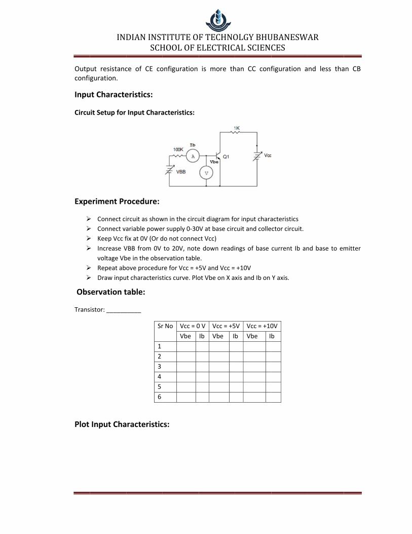
ut Characte
it Setup for
eriment Pr
Connect ci
Connect va
Keep Vcc f
Increase V
voltage Vb
Repeat ab
Draw inpu
servation t
istor: ______
Input Cha
DIANINSTSCH
ce of CE co
eristics:
Input Chara
rocedure:
ircuit as show
ariable powe
fix at 0V (Or d
VBB from 0V
be in the obse
ove procedur
t characterist
table:
_____
Sr
1
2
3
4
5
6
aracteristic
TITUTEOHOOLOFE
onfiguration
acteristics:
wn in the circu
r supply 0‐30
do not connec
to 20V, note
ervation table
re for Vcc = +
tics curve. Plo
r No Vcc = 0
Vbe
cs:
FTECHNOELECTRIC
is more th
uit diagram fo
0V at base circ
ct Vcc)
e down readi
e.
5V and Vcc =
ot Vbe on X ax
0 V Vcc = +5
Ib Vbe Ib
OLGYBHUALSCIENC
han CC conf
or input chara
cuit and colle
ings of base
+10V
xis and Ib on
5V Vcc = +10
b Vbe I
UBANESWCES
figuration a
acteristics
ctor circuit.
current Ib an
Y axis.
0V
b
WAR
and less tha
nd base to em
an CB
mitter
Inpu
Circu
Expe
Obse
Trans
Plot
Conc
IND
ut Characte
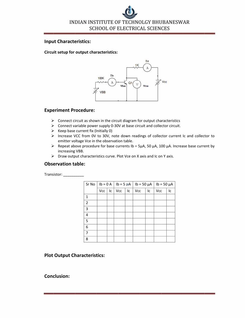
it setup for
eriment Pr
Connect ci Connect va Keep base Increase V
emitter vo Repeat ab
increasing Draw outp
ervation ta
istor: ______
Output Ch
clusion:
DIANINSTSCH
eristics:
output char
rocedure:
ircuit as showariable powe current fix (IVCC from 0V oltage Vce in tove procedurVBB.
put characteri
able:
_____
Sr No
1
2
3
4
5
6
7
8
haracterist
TITUTEOHOOLOFE
racteristics:
wn in the circur supply 0‐30nitially 0) to 30V, notethe observatire for base cu
istics curve. P
Ib = 0 A Ib
Vcc Ic V
tics:
FTECHNOELECTRIC
uit diagram fo0V at base circ
e down readon table. urrents Ib = 5
Plot Vce on X
b = 5 A Ib =
cc Ic Vcc
OLGYBHUALSCIENC
or output chacuit and colle
ings of collec
5µA, 50 µA, 10
axis and Ic on
= 50 µA Ib =
c Ic Vcc
UBANESWCES
aracteristics ctor circuit.
ctor current
00 µA. Increa
n Y axis.
= 50 µA
c Ic
WAR
Ic and collec
ase base curre
tor to
ent by
Aim ampl
Appa
Theosupplyline. Icycle,upwagain).collecnegatreducdrop applieto cuprovidWithoto prowhich
CE amcouplfrequis highat lowcapacdoes transitransi
If we positi
IND
of Experifier. To mea
aratus Req
Sl. No.
ory: Commo
y to amplify in the circuit forward biasrd direction Collector resctor voltage. tive cycle, forces (Q point mIcRc reducesed base voltarrent gain B.des large voltout emitter reovide stabilith provides AC
mplifier does ing capacitorency, hence h). There is vw frequenciecitances. Audnot provideistors are BCistors like BF1
apply large sve peak and
DIANINSTSCH
riment: Toasure gain o
quired:
Name of A
on emitter am
nput AC signshown, voltas of base‐emon load line sistor drop IcThus during rward bias of moves downs and collectoge because le. This large ctage output. Tesistance gainty. To compeC ground to th
not provide rs reduces gaemitter bypavoltage drop aes. Gain of Cio frequencye large voltaC147/BC148/B194/BF594/B
signal at the cut‐off regio
TITUTEOHOOLOFE
EXPE
observe in
f amplifier a
Apparatus
mplifier is used
al. Biasing of ge divider biaitter junctionand collectoRc increases positive inpbase‐emitter
side). Due to dor voltage incess base currcollector currThus CE ampn of amplifierensate effect he emitter. Th
constant volin of amplifieass capacitor across coupliCE amplifier y transistors age gain for BC547/BC548F200 provide
input of CE aon during ne
FTECHNOELECTRIC
RIMENT
nput‐output
at different f
d to amplify w
transistor is das is formed un increases anr current incdue to incre
put cycle, wer junction anddecrease in ccreases. Chanrent variationrent further lifier providesr is highest bof emitter r
his will increa
ltage gain at er at low freqdoes not prong capacitor also reduceslike AC127, Afrequency
8 provides vos gain at radi
amplifier, traegative peak
OLGYBHUALSCIENC
NO. 4
t waveform
frequencies
Specification
weak signal. It
done to tie Qusing resistornd base currereases times ease in collece get negativd base currenollector currenge in collect causes largemultiplied bys voltage gainut it is not stresistance emse gain of am
all frequenciuency. Reactovide perfect at low freques at very higAC128 worksgreater thanoltage gain uo frequencies
ansistor drive(Q point rea
UBANESWCES
s of comm
and plot freq
Q
t utilizes ene
Q point at the rs 10K and 2.2ent increasesthan base cu
ctor current Ie output cycnt will reduceent, collectoror voltage is e collector cury collector ren and amplifietable. Emittermitter bypassmplifier.
ies. Due to etance of capaAC ground (Eency becausegh frequencys for audio frn 20 KHz. Mup to 500 KHs in the MHz
n into saturaaches to satu
WAR
mon emitter
quency resp
Quantity
rgy from DC p
middle of the2K. During po. Q point mourrent. ( is cuc. This will recle. When ine. Collector cur resistance vomuch higherrrent variatioesistance Rc es the input sr resistance iss capacitor is
emitter bypascitor is high aEmitter impee of high reacy because of requency ranMedium freqHz. High freqrange.
ation region duration and c
r (CE)
ponse
power
e load ositive oves in urrent educe put is urrent oltage r than on due which signal. s used s used
ss and at low dance ctance stray
nge. It uency uency
during cut‐off
pointsand e
Circu
Expe
Obse
InputSr No
1
2
3
4
5
6
7
8
9
10
Draw
or us
Conc
IND
s). Due to thinsure that tra
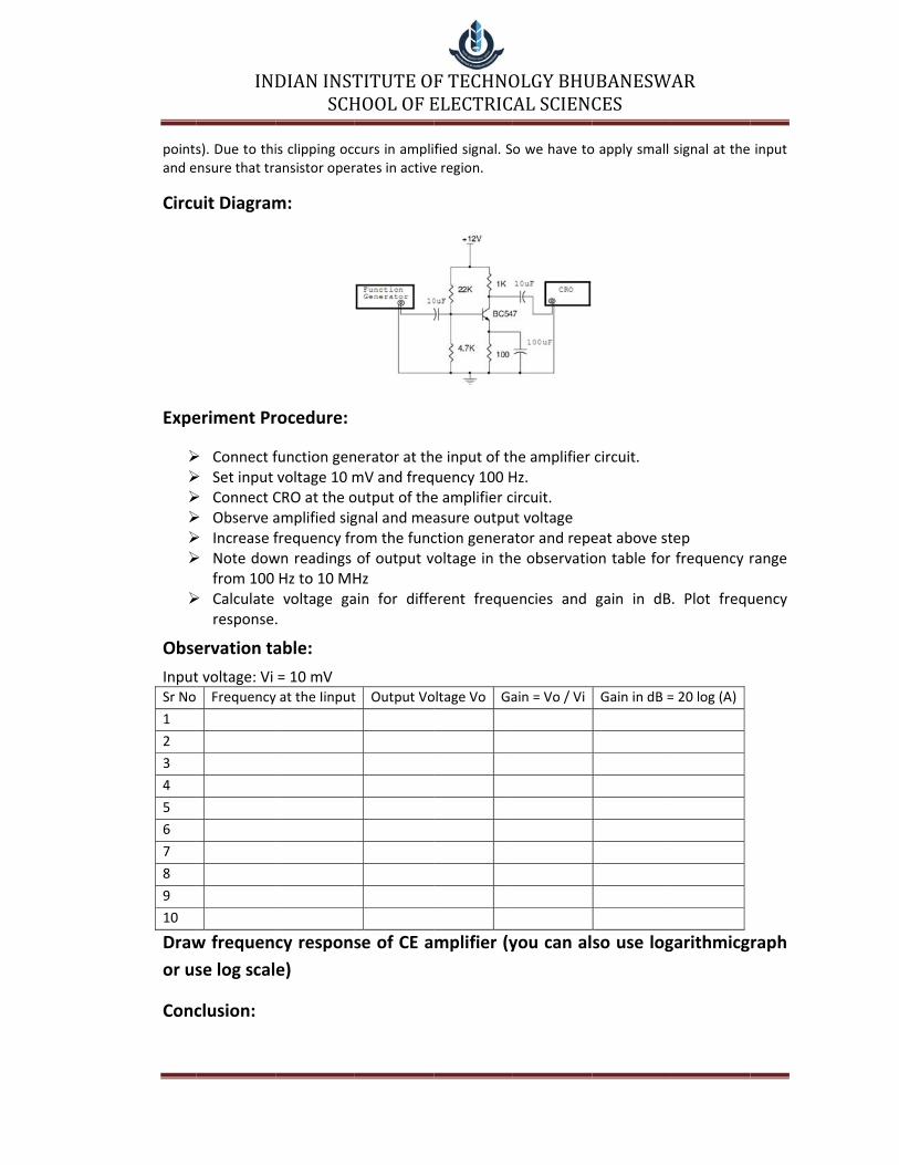
uit Diagram
eriment Pr
Connect f Set input Connect C Observe a Increase f Note dow
from 100 Calculate
response.
ervation ta
t voltage: Vi Frequency
w frequen
se log scal
clusion:
DIANINSTSCH
is clipping ocansistor oper
m:
rocedure:
function genvoltage 10 mCRO at the oamplified sigfrequency frwn readings Hz to 10 MHvoltage ga
.
able:
= 10 mV y at the Iinput
cy respons
e)
TITUTEOHOOLOFE
curs in amplirates in active
nerator at thmV and freqoutput of thegnal and mearom the funcof output vHz ain for diffe
t Output Vo
se of CE a
FTECHNOELECTRIC
fied signal. Se region.
e input of thuency 100 He amplifier casure outpuction generaoltage in th
erent freque
oltage Vo Ga
mplifier (y
OLGYBHUALSCIENC
o we have to
he amplifier Hz. circuit. t voltage ator and repee observatio
encies and
ain = Vo / Vi
you can al
UBANESWCES
o apply small
circuit.
eat above ston table for
gain in dB
Gain in dB =
so use log
WAR
signal at the
tep frequency r
. Plot frequ
= 20 log (A)
garithmicg
input
range
uency
raph
Aim
inver
Appa
Theo
shift
The v
The R
volta
phase
exact
total
the s
Circu
IND
of Experim
rting and sum
aratus Req
Sl. No.
ory: RC‐Pha
feedback Ne
values of R a
RC ladder ne
ge for the g
e shift from
tly 360º or
loop gain o
inusoidal os
uit Diagram
DIANINSTSCH
ment: To s
mmer.
quired:
Name of A
ase shift Osc
etworks the
and C are c
etwork prod
given freque
the base of
0º. This sat
of this circuit
cillations. Th
m:
TITUTEOHOOLOFE
EXPE
study the va
Apparatus
illator has a
e output of t
hosen such
duces a tota
encies. Since
f the transis
tisfies the B
t is greater
he frequency
FTECHNOELECTRIC
RIMENT
arious applic
CE amplifie
the last stag
that the ph
al phase shif
e CE Amplifie
stor around
arkhausen c
than or equ
y of oscillati
OLGYBHUALSCIENC
NO. 5
cation of Op
Specification
r followed b
ge is return t
hase shift of
ft of 180º b
er produces
the circuit a
condition fo
ual to 1, this
ons of RC‐Ph
UBANESWCES
pamp such a
Q
by three sect
to the input
each RC se
etween its i
s 180 º phas
and back to
or sustaining
s condition u
hase Shift Os
WAR
as inverting,
Quantity
tions of RC p
t of the amp
ection is 60º
input and o
ses shift the
o the base w
g oscillations
used to gen
scillator is,
non‐
phase
plifier.
.Thus
utput
total
will be
s and
nerate

Expe
Obse
Theo
R = 1
Pract
Sl No
1
2
3
Wav
Conc
IND
eriment Pr
Make the Observe t Calculate Calculate
between formula.
ervation:
retical Calcu
0 kΩ, C = 0.0
tical Calculat
o R
10 k
10 k
10 k
veforms to Ou Ou
clusion:
DIANINSTSCH
rocedure:
e connectionthe output sthe frequenthe phase sthe final wa
ulations:
001 μf
tions:
C
kΩ 0.0
kΩ 0.0
kΩ 0.0
o be observutput wavefutput wavef
TITUTEOHOOLOFE
n as per the cignal and noncy of oscillahift at each veform and
Ɵ
f (
001 μf
001 μf
001 μf
ved: form form and wa
FTECHNOELECTRIC
circuit diagraote down theations theoreRC section bthe wavefo
= (TP /Td )*3
Observed)
aveform at e
OLGYBHUALSCIENC
am shown ae output ametically and vby measurinrm at that se
360
Td = 1/f (Observed)
ach section
UBANESWCES
bove. mplitude and verify it pracg the time section by us
)Tp(Observ
WAR
time periodctically (f=1/hifts (Tp) ing the belo
ved) Ɵ
d Td. /Td).
ow
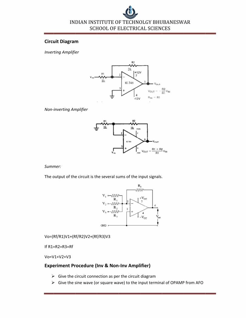
Aim inver
Appa
Theo
Inver
The connconnVout
Vout
Non‐I
Here given
Vout
Pin D
IND
of Experimrting and sum
aratus Req
Sl. No.
1 IC
2 Res
3 Sig
4 CRO
5 Reg
6 Du
7 Bre
8 Wi
9
ory:
rting Amplifie
source Vin ected betwected to invof the inver
= ‐[R2/R1]*
Inverting Am
source Vin n by
= [1+(R2/R1
Details of IC 7
DIANINSTSCH
ment: To smmer.
quired:
Name of AComp
sistor
nal Generato
O
gulated Powe
al Power Sup
ead Board
res
er
is connecteween input verting termirting amplifie
Vin
mplifier:
is connecte
1)]*Vin
741
TITUTEOHOOLOFE
EXPE
study the va
Apparatus / ponent
or
er Supply
pply
ed in seriesterminal aninal. The noner is given b
d with non‐
FTECHNOELECTRIC
RIMENT
arious applic
s with R1 and invertingn‐inverting ty
inverting inp
OLGYBHUALSCIENC
NO. 6
cation of Op
Specification
741
2 k 1 k
0 to 30 V
‐12 V, +12 V
and R2. Theg input termterminal is g
put termina
UBANESWCES
pamp such a
Q
A
e feedback minal. The grounded. Th
l. The outpu
WAR
as inverting,
Quantity
1
1 2
1
1
1
1
1
As Reqd
resistance resistance he output vo
ut voltage Vo
non‐
R2 is R1 is oltage
out is
Circu
Inver
Non‐i
Summ
The o
Vo=(R
If R1=
Vo=V
Expe
IND
uit Diagram
rting Amplifie
inverting Am
mer:
output of the
Rf/R1)V1+(R
=R2=R3=Rf
V1+V2+V3
eriment Pr
Give the c
Give the s
DIANINSTSCH
m
er
mplifier
e circuit is th
Rf/R2)V2+(Rf
rocedure (I
circuit conne
sine wave (o
TITUTEOHOOLOFE
he several su
f/R3)V3
Inv & Non
ection as per
or square wa
FTECHNOELECTRIC
ums of the in
‐Inv Ampli
r the circuit
ave) to the in
OLGYBHUALSCIENC
nput signals.
ifier)
diagram
nput termina
UBANESWCES
.
al of OPAMP
WAR
P from AFO

Expe
Obse
Inv A
Input
Outp
Non I
Input
Outp
Obse
Input
1 1.5 2 2.5 3
Conc
IND
Set the ou
Observe t
Note dow
Find the v
Draw the
eriment Pr
Connectio According The dc vo The dc vo
into satur The outp
sum of th Compare
ervation T
mp
t
ut
Inv Amp
t
ut
ervation T
t Voltage
clusion:
DIANINSTSCH
utput and in
the amplitud
wn the phase
voltage gain
input and o
rocedure (A
ons are giveng to the gainoltages are goltage levelsration ut voltage ie inputs the theoret
able (Inv &
X
No of Div
able (Inv &
Gain Pra
TITUTEOHOOLOFE
put wavefor
de and time
e shift of the
(Vout/Vin)
output wavef
Adder):
n as per the n, find the reiven at the is are minim
s measured
ical and prac
& Non‐Inv
‐ Axis
Time/Div
& Non‐Inv
actical Outp
FTECHNOELECTRIC
rms in CRO
of the outpu
e input and o
forms
circuit diagrsistors valuenputs ized such th
d with the h
ctical value
Amplifier)
Time
v
Amplifier)
ut Voltage
OLGYBHUALSCIENC
ut and input
output wave
ram e
hat their sum
help of a mu
):
Y
No of Div
):
Theoretic
UBANESWCES
t waveforms
forms
m does not
ultimeter. It
‐ Axis
Volt/Div
cal Output V
WAR
s
take the Op
will be neg
Amplit
v
Voltage
pamp
gative
tude
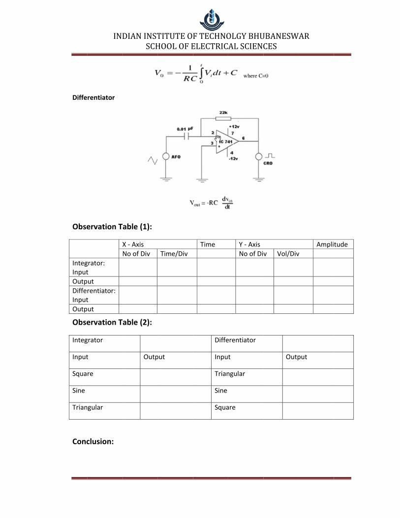
Aim Differ
Appa
Theo
produ
conta
math
input
Pin D
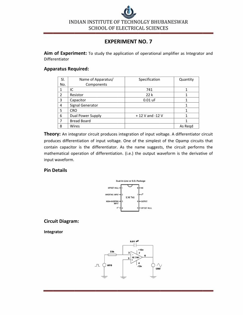
Circu
Integ
IND
of Experimrentiator
aratus Req
Sl. No.
1 IC
2 Res
3 Cap
4 Sig
5 CR
6 Du
7 Bre
8 Wi
ory: An inte
uces differe
ain capacito
hematical op
t waveform.
Details
uit Diagram
grator
DIANINSTSCH
ment: To s
quired:
Name of ACompo
sistor
pacitor
gnal Generato
O
al Power Sup
ead Board
res
egrator circu
ntiation of
or is the dif
peration of
m:
TITUTEOHOOLOFE
EXPE
study the ap
Apparatus/ onents
or
pply
uit produces
input voltag
fferentiator.
differentiati
FTECHNOELECTRIC
RIMENT
pplication of
+
integration
ge. One of t
. As the na
ion. (i.e.) th
OLGYBHUALSCIENC
NO. 7
f operationa
Specification
741
22 k
0.01 uF
12 V and ‐12
of input vo
the simplest
ame suggest
e output w
UBANESWCES
l amplifier a
Q
V
A
oltage. A diff
t of the Opa
ts, the circu
aveform is
WAR
as Integrato
Quantity
1
1
1
1
1
1
1
As Reqd
ferentiator c
amp circuits
uit perform
the derivati
r and
circuit
s that
s the
ive of
Diffe
Obse
IntegInput
Outp
DifferInput
Outp
Obse
Integ
Input
Squa
Sine
Trian
Conc
IND
rentiator
ervation T
X
grator: t
ut
rentiator: t
ut
ervation T
grator
t
re
gular
clusion:
DIANINSTSCH
able (1):
X ‐ Axis
No of Div
able (2):
Outp
TITUTEOHOOLOFE
Time/Div
put
FTECHNOELECTRIC
Time
Diffe
Inpu
Trian
Sine
Squa
OLGYBHUALSCIENC
Y ‐ Axis
No of Di
erentiator
t
ngular
are
UBANESWCES
v Vol/Div
Outp
WAR
Ampli
v
put
tude

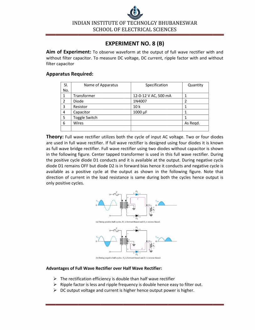
Aim withofilter
Appa
Theoto coequiposcillexammeasand pfirst bused rectifrectifrectif
Wor
In havoltacyclefigurecompand pvoltapasse
Half Filterthis p
IND
of Experimout filter capcapacitor.
aratus Req
Sl. No.
1 Tra
2 Dio
3 Res
4 Cap
ory: One of onvert AC ipment. Thisators, ampl
mple, we casuring instruperformanceblock of DC to convert
fier needs ufier. Rectifiefier. In this e
rking Princ
lf wave rectge (negative. The circuite. During ppared with tpositive cyclge, anode ises through t
wave rectifir capacitor ispractical.
DIANINSTSCH
ment: To opacitor. To m
quired:
Name of A
ansformer
ode
sistor
pacitor
the very im
into DC. DCs is becausifiers and soan’t think ouments like e of the elecpower supp ac voltageunidirectionaer broadly dexperiment,
iple of Hal
tifier only hae cycle) is not diagram ofpositive halfhe cathode.e develops as negative whe diode he
ier without s used to ob
TITUTEOHOOLOFE
EXPERI
observe wav
measure DC
Apparatus
portant app
C Power sue it provido on. In eleof televisionCRO, multi‐ctronic systeply is rectifie or currental device. Didivided into you will con
lf Wave Re
alf cycle of aot used. Onf half wave rf cycle of t. Diode is inacross the loith respectence output v
filter capacbtain smooth
FTECHNOELECTRIC
MENT NO
eform at th
voltage, DC
230V/1
1N4007
10 k
100 uF
plications of
upply is thees power ctronic equn, computermeter etc. wem proper der. Rectifier into unidiriode has untwo catego
nstruct half w
ectifier:
applied AC vly one dioderectifier withthe input v forward biaoad resistand to cathodevoltage is ze
citor converth DC voltage
OLGYBHUALSCIENC
O. 8 (A)
e output of
C current, rip
Specification
12V, 500 mA
7
diode is in D
e importantto energizeipment, D.Cr, radio, telwithout DC design of pomay be defrectional vonidirectional ories: Half wwave rectifie
voltage is use is used whhout capacitoltage anodas and currece RL. Duringe and diode ero.
t AC voltagee. Construct
UBANESWCES
half wave r
pple factor w
Q
DC power su
element oe all electroC. power supephone, mpower suppwer supply fined as an ltage or cuproperty hewave rectifieer.
sed. Anothehich conducttor is shownde of the dent passes thg negative his in reverse
e into pulsat following c
WAR
rectifier with
with and wit
Quantity
1
1
1
1
pply as a rec
of any electonic circuitspply is mustobile as weply. The reliais necessaryelectronic drrent. Essenence suitaber and full
r half cycle ts during pon in the follodiode is pohrough the dhalf cycle of e bias. No cu
ating DC vocircuit to per
h and
thout
ctifier
tronic s like t. For ell as ability y. The device ntially le for wave
of AC ositive owing ositive diode input urrent
ltage. rform

Circu
Proc
Consthalf w
Wav
[1] WInputOutp[2] WInputOutp
Obse
[1] WAC InDC ouDC cuAC ouRippl[2] WAC InDC ouDC cuAC ouRippl
Conc
IND
uit Diagram
cedure:
truct circuit wave rectifie
veforms to
Without filtert Waveform ut waveform
With filter cat Waveform ut waveform
ervations:
Without filternput voltage utput voltagurrent: IDC=_utput voltage factor: (Vr
With filter canput voltage utput voltagurrent: IDC=_utput voltage factor: (Vr
clusion:
DIANINSTSCH
m:
on the geneer without fi
o be observ
r capacitor: at secondarm: pacitor: at secondarm:
r capacitor (rms) Vrms=
ge VDC= ______________ge (Ripple vor/VDC) = ___pacitor (rms) Vrms=
ge VDC= ______________ge (Ripple vor/VDC) = ___
TITUTEOHOOLOFE
eral purposelter capacito
ved:
ry of transfo
ry of transfo
= _________________ _____ oltage) Vr: _____________
= _________________ _____ oltage) Vr: _____________
FTECHNOELECTRIC
e PCB. Keep tor and ON to
rmer:
rmer:
___
___________
___
___________
OLGYBHUALSCIENC
toggle switco connect filt
UBANESWCES
h OFF to perter capacito
WAR
rform practir.
cal of
Aim withofilter
Appa
Theoare uas fuin thethe pdiodeavailadireconly
Adva
IND
of Experimout filter capcapacitor
aratus Req
Sl. No.
1 Tra
2 Dio
3 Res
4 Cap
5 Tog
6 Wi
ory: Full waused in full wll wave bridge following fpositive cyclee D1 remainable as a ption of currpositive cycl
antages of Fu
The rectif Ripple fac DC outpu
DIANINSTSCH
ment: To opacitor. To m
quired:
Name of A
ansformer
ode
sistor
pacitor
ggle Switch
res
ave rectifier
wave rectifiege rectifier. figure. Cente diode D1 cs OFF but diositive cyclerent in the lles.
ull Wave Re
fication efficctor is less at voltage an
TITUTEOHOOLOFE
EXPERI
observe wav
measure DC
Apparatus
utilizes bot
er. If full wavFull wave reer tapped tconducts anode D2 is in e at the ouoad resistan
ctifier over
ciency is dound ripple fred current is
FTECHNOELECTRIC
MENT NO
veform at th
voltage, DC
12‐0‐12
1N4007
10 k
1000 µ
h the cycle
ve rectifier iectifier usingransformer d it is availaforward bia
utput as shonce is same
Half Wave R
ble than halequency is dohigher henc
OLGYBHUALSCIENC
O. 8 (B)
he output of
C current, rip
Specification
2 V AC, 500 m
7
F
of input AC
s designed ug two diodeis used in thable at the oas hence it coown in the during both
Rectifier:
lf wave rectiouble hencece output po
UBANESWCES
f full wave r
pple factor w
Q
mA 1
2
1
1
1
As R
voltage. Tw
using four ds without cahis full waveoutput. Durionducts andfollowing fh the cycles
ifier e easy to filteower is highe
WAR
rectifier with
with and wit
Quantity
Reqd.
wo or four d
iodes it is kapacitor is se rectifier. Dng negative d negative cyfigure. Notes hence outp
er out. er.
h and
thout
iodes
nown hown During cycle ycle is e that put is
Disad
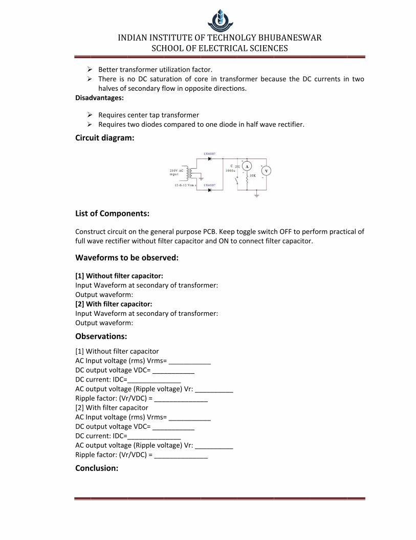
Circu
List o
Constfull w
Wav
[1] WInputOutp[2] WInputOutp
Obse
[1] WAC InDC ouDC cuAC ouRippl[2] WAC InDC ouDC cuAC ouRippl
Conc
IND
Better tra There is
halves of dvantages:
Requires Requires
uit diagram
of Compon
truct circuit wave rectifie
veforms to
Without filtert Waveform ut waveform
With filter cat Waveform ut waveform
ervations:
Without filternput voltage utput voltagurrent: IDC=_utput voltage factor: (Vr
With filter capnput voltage utput voltagurrent: IDC=_utput voltage factor: (Vr
clusion:
DIANINSTSCH
ansformer utno DC satursecondary f
center tap ttwo diodes c
m:
nents:
on the gener without filt
o be observ
r capacitor: at secondarm: pacitor: at secondarm:
r capacitor (rms) Vrms=
ge VDC= ______________ge (Ripple vor/VDC) = ___pacitor (rms) Vrms=
ge VDC= ______________ge (Ripple vor/VDC) = ___
TITUTEOHOOLOFE
tilization facration of coflow in oppo
ransformercompared to
eral purposeter capacito
ved:
ry of transfo
ry of transfo
= _________________ _____ oltage) Vr: _____________
= _________________ _____ oltage) Vr: _____________
FTECHNOELECTRIC
ctor. ore in transfsite directio
o one diode
e PCB. Keep tr and ON to
rmer:
rmer:
___
___________
___
___________
OLGYBHUALSCIENC
former becaons.
in half wave
toggle switcconnect filt
UBANESWCES
ause the DC
e rectifier.
h OFF to perer capacitor
WAR
C currents in
rform practir.
n two
cal of
Aim withofilter
Appa
Theoboth figure
The cdiagotwo econdin ser
IND
of Experiout filter capcapacitor
aratus Req
Sl. No.
1 Tra
2 Dio
3 Res
4 Cap
5 Tog
6 Wi
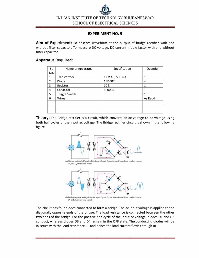
ory: The Brhalf cycles oe.
circuit has foonally opposends of the uct, wherearies with the
DIANINSTSCH
iment: To pacitor. To m
quired:
Name of A
ansformer
ode
sistor
pacitor
ggle Switch
res
idge rectifie
of the input
our diodes cosite ends of tbridge. For tas diodes D3e load resista
TITUTEOHOOLOFE
EXPE
observe wa
measure DC
Apparatus
er is a circuit
ac voltage.
onnected tothe bridge. Tthe positive 3 and D4 remance RL and
FTECHNOELECTRIC
ERIMENT N
aveform at t
voltage, DC
12 V AC
1N4007
10 k
1000 µ
t, which con
The Bridge
form a bridThe load reshalf cycle o
main in the Ohence the lo
OLGYBHUALSCIENC
NO. 9
the output
C current, rip
Specification
C, 500 mA
7
F
nverts an ac
rectifier circ
ge. The ac insistance is cof the input aOFF state. Toad current
UBANESWCES
of bridge r
pple factor w
Q
1
4
1
1
1
As R
c voltage to
cuit is shown
nput voltageonnected beac voltage, dhe conductiflows throu
WAR
ectifier with
with and wit
Quantity
Reqd
dc voltage
n in the follo
e is applied tetween the diodes D1 anng diodes wgh RL.
h and
thout
using
owing
to the other nd D2 will be
For tand resistprevi
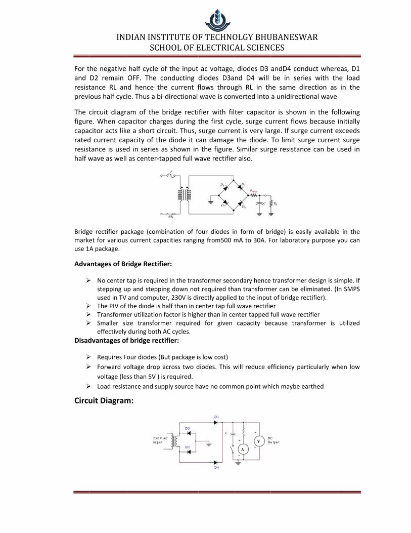
The cfigurecapacratedresisthalf w
Bridgemarkeuse 1A
Adva
Disad
Circu
IND
he negativeD2 remain tance RL anous half cyc
circuit diagre. When capcitor acts likd current catance is usewave as well
e rectifier paet for variousA package.
antages of Br
No center stepping uused in TV
The PIV of Transform Smaller si
effectively
dvantages o
Requires F
Forward v
voltage (le
Load resist
uit Diagram
DIANINSTSCH
half cycle oOFF. The c
nd hence thle. Thus a bi
ram of the pacitor charke a short cipacity of thd in series al as center‐ta
ackage (combs current cap
ridge Rectifi
tap is requireup and steppiV and computthe diode is er utilization ize transformy during both
f bridge rect
Four diodes (B
voltage drop
ess than 5V ) i
tance and sup
m:
TITUTEOHOOLOFE
of the inputconducting he current f‐directional
bridge rectirges during trcuit. Thus, e diode it cas shown inapped full w
bination of fopacities rangin
ier:
ed in the traning down noter, 230V is dihalf than in cfactor is highmer requiredAC cycles.
tifier:
But package i
across two d
is required.
pply source h
FTECHNOELECTRIC
ac voltage,diodes D3aflows throuwave is con
fier with filthe first cycsurge currecan damage the figure.
wave rectifie
our diodes inng from500 m
nsformer secot required tharectly appliedcenter tap fullher than in ced for given
s low cost)
diodes. This w
have no comm
OLGYBHUALSCIENC
diodes D3 nd D4 will gh RL in thnverted into
ter capacitocle, surge cunt is very lathe diode. Similar surgr also.
n form of brmA to 30A. F
ondary hencean transformd to the inputl wave rectifieenter tapped fcapacity be
will reduce e
mon point wh
UBANESWCES
andD4 condbe in serie
he same dira unidirectio
or is shown urrent flowsrge. If surgeTo limit surge resistanc
ridge) is easiFor laboratory
transformer mer can be elit of bridge recer full wave rectecause transf
fficiency part
ich maybe ea
WAR
duct whereaes with the rection as inonal wave
in the follo because ine current excrge current e can be us
ly available iy purpose yo
design is simminated. (In ctifier).
tifier former is ut
ticularly whe
arthed
as, D1 load
n the
owing itially ceeds surge sed in
in the ou can
mple. If SMPS
tilized
en low

Expe
Const
wave
Wav
[1] WInput Outpu[2] WInput Outpu
Obse
[1] W
AC Inp
DC ou
DC cu
AC ou
Ripple
[2] W
AC Inp
DC ou
DC cu
AC ou
Ripple
Conc
IND
erimental P
truct circuit o
rectifier with
veforms to
Without filter cWaveform atut waveform:
With filter capaWaveform atut waveform:
ervations:
Without filter c
put voltage (r
utput voltage
urrent: IDC=__
utput voltage
e factor: (Vr/V
With filter capa
put voltage (r
utput voltage
urrent: IDC=__
utput voltage
e factor: (Vr/V
clusion:
DIANINSTSCH
Procedure
on the gener
hout filter cap
o be observ
capacitor: t secondary o: acitor: t secondary o:
capacitor
rms) Vrms= _
VDC= ______
___________
(Ripple volta
VDC) = _____
acitor
rms) Vrms= _
VDC= ______
___________
(Ripple volta
VDC) = _____
TITUTEOHOOLOFE
e:
ral purpose P
pacitor and O
ved:
of transforme
of transforme
___________
______
___
ge) Vr: _____
__________
___________
______
___
ge) Vr: _____
__________
FTECHNOELECTRIC
PCB. Keep to
N toconnect
er:
er:
______
______
OLGYBHUALSCIENC
oggle switch O
filter capacito
UBANESWCES
OFF toperfor
or.
WAR
rm practical oof full

Aim and v
Appa
Pin C2 inpu
2 inpu
2 inpu
IND
of Experimverify their t
aratus Req
Sl. No.
1 IC
2 IC
3 IC
4 IC
5 IC
6 Bre
7 Wi
Configuratut OR Gate (I
ut AND Gate
ut NOR Gate
DIANINSTSCH
ment: (a) Truth tables
quired:
Name of A
ead Board
res
tion and TrC 7432)
(IC 7408)
(IC 7402)
TITUTEOHOOLOFE
EXPERIM
To verify log
Apparatus
routh Tabl
FTECHNOELECTRIC
MENT NO
ic gates OR,
e:
A
0
0
1
1
A
0
0
1
1
A
0
0
1
1
OLGYBHUALSCIENC
O. 10 (A)
, AND, NOT,
Specification
7408
7402
7400
7486
7432
Truth Tab
B
0
1
0
1
Truth Ta
B
0
1
0
1
Truth Tab
B
0
1
0
1
UBANESWCES
, NOR, NAN
Q
A
le
O/
able
O
ble
O
WAR
D gates usin
Quantity
1
1
1
1
1
1
s Reqd.
/P
O/P
/P
ng ICs
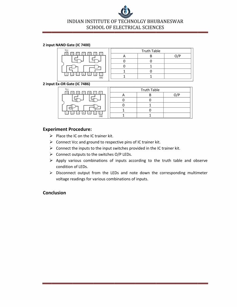
2 inpu
2 inpu
Expe
Conc
IND
ut NAND Gat
ut Ex‐OR Gate
eriment Pr
Place the
Connect V
Connect t
Connect o
Apply va
condition
Disconnec
voltage re
clusion
DIANINSTSCH
e (IC 7400)
e (IC 7486)
rocedure:
IC on the IC
Vcc and grou
the inputs to
outputs to th
rious comb
of LEDs.
ct output fr
eadings for v
TITUTEOHOOLOFE
C trainer kit.
und to respe
o the input s
he switches
inations of
rom the LE
various comb
FTECHNOELECTRIC
A
0
0
1
1
A
0
0
1
1
ective pins o
witches pro
O/P LEDs.
inputs acco
Ds and not
binations of
OLGYBHUALSCIENC
Truth Tab
B
0
1
0
1
Truth Tab
B
0
1
0
1
f IC trainer k
vided in the
ording to th
te down the
inputs.
UBANESWCES
ble
O
ble
O/
kit.
IC trainer k
he truth ta
e correspon
WAR
O/P
/P
it.
ble and ob
nding multim
serve
meter
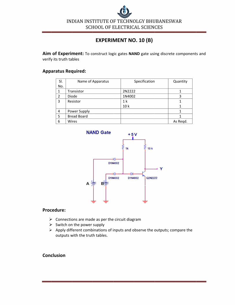
Aim verify
Appa
Proc
Conc
IND
of Experimy its truth ta
aratus Req
Sl. No.
1 Tra
2 Dio
3 Res
4 Pow
5 Bre
6 Wi
cedure:
Connectio Switch on Apply diff
outputs w
clusion
DIANINSTSCH
ment: To cobles
quired:
Name of A
ansistor
ode
sistor
wer Supply
ead Board
res
ons are madn the power ferent combwith the trut
TITUTEOHOOLOFE
EXPERIM
onstruct log
Apparatus
e as per thesupply inations of ih tables.
FTECHNOELECTRIC
MENT NO
gic gates NA
2N2222
1N4002
1 k10 k
e circuit diag
nputs and o
OLGYBHUALSCIENC
O. 10 (B)
AND gate usi
Specification
2
2
ram
observe the o
UBANESWCES
ng discrete
Q
A
outputs; com
WAR
component
Quantity
1
3
1 1
1
1
As Reqd.
mpare the
s and