automatic synthesis of sequential circuits for low power dissipation
TRANSCRIPT

AUTOMATIC SYNTHESIS OF SEQUENTIAL CIRCUITS
FOR LOW POWER DISSIPATION
a dissertation
submitted to the department of electrical engineering
and the committee on graduate studies
of stanford university
in partial fulfillment of the requirements
for the degree of
doctor of philosophy
Luca Benini
February, 1997

c Copyright 1997
by
Luca Benini
ii

I certify that I have read this thesis and that in my opin-
ion it is fully adequate, in scope and in quality, as a
dissertation for the degree of Doctor of Philosophy.
Giovanni De Micheli(Principal Adviser)
I certify that I have read this thesis and that in my opin-
ion it is fully adequate, in scope and in quality, as a
dissertation for the degree of Doctor of Philosophy.
Teresa Meng(Associate Adviser)
I certify that I have read this thesis and that in my opin-
ion it is fully adequate, in scope and in quality, as a
dissertation for the degree of Doctor of Philosophy.
Stephen Boyd
Approved for the University Committee on Graduate
Studies:
iii

Abstract
In high-performance digital CMOS systems, excessive power dissipation reduces re-
liability and increases the cost imposed by cooling systems and packaging. Power is
obviously is the primary concern for portable applications, since battery technology
cannot keep the fast pace imposed by Moore's Law, and there is large demand for
devices with light batteries and long time between recharges.
Computer-Aided Engineering is probably the only viable paradigm for designing
state-of-the art VLSI and ULSI systems, because it allows the designer to focus on
the high-level trade-o�s and to concentrate the human e�ort on the most critical
parts of the design. We present a framework for the computer-aided design of low-
power digital circuits. We propose several techniques for automatic power reduction
based on paradigms which are widely used by designers. Our main purpose is to
provide the foundation for a new generation of CAD tools for power optimization
under performance constraints. In the last decade, the automatic synthesis and op-
timization of digital circuits for minimum area and maximum performance has been
extensively investigated. We leverage the knowledge base created by such research,
but we acknowledge the distinctive characteristics of power as optimization
iv

Dedication
To Natasha, with gratitude and love.
v

Acknowledgments
I have many people to thank for this dissertation. First of all, my advisor, Professor
Giovanni De Micheli, who guided my e�orts and never denied his help. I am very
grateful to the members of my reading committee, Professor Teresa Meng and Pro-
fessor Stephen Boyd, for the time and patience spent in reading these pages. This
research was sponsored by a scholarship from NSF, under grant MIP-9421129. I wish
to thank NSF for the economic support that made possible this work.
I also wish to thank all current and past members of the CAD group: Claudionor
Coelho, David Filo, David Ku, Vincent Mooney, Polly Siegel (who also read part
of this thesis), Matja Siljak, Frederick Vermeulen, Patrick Vuillod and Jerry Yang.
Their help has been invaluable in many occasions.
Special thanks to my �rst mentor, Professor Bruno Ricc�o and to my friends and
colleagues at DEIS, Universit�a di Bologna. I am also deeply in debt with the friends
of Politecnico di Torino for long, sleepless nights of work. I would especially like
to mention two good friends and great co-workers, Alessandro Bogliolo and Enrico
Macii, for sharing with me the pains of bringing ideas to practice.
Lastly, I am deeply in debt with my family who gave me support during the
hard moments, and with my wife Natasha, for her love and the wonderful gift of her
presence.
vi

Contents
Abstract iv
Dedication v
Acknowledgments vi
1 Introduction 1
1.1 Sources of power consumption : : : : : : : : : : : : : : : : : : : : : : 3
1.2 Design techniques for low power : : : : : : : : : : : : : : : : : : : : : 9
1.2.1 Power minimization by frequency reduction : : : : : : : : : : 9
1.2.2 Power minimization by voltage scaling : : : : : : : : : : : : : 11
1.2.3 Power optimization by capacitance reduction : : : : : : : : : : 15
1.2.4 Power optimization by switching activity reduction : : : : : : 18
1.2.5 Revolutionary approaches : : : : : : : : : : : : : : : : : : : : 20
1.3 CAD techniques for low power : : : : : : : : : : : : : : : : : : : : : : 23
1.3.1 High-level optimizations : : : : : : : : : : : : : : : : : : : : : 25
1.3.2 Logic-level sequential optimizations : : : : : : : : : : : : : : : 28
1.3.3 Power management schemes : : : : : : : : : : : : : : : : : : : 31
1.4 Thesis contribution : : : : : : : : : : : : : : : : : : : : : : : : : : : : 33
1.5 Outline of the following chapters : : : : : : : : : : : : : : : : : : : : 35
vii

2 Background 37
2.1 Boolean algebra and �nite state machines : : : : : : : : : : : : : : : : 37
2.1.1 Boolean algebra : : : : : : : : : : : : : : : : : : : : : : : : : : 38
2.1.2 Finite state machines : : : : : : : : : : : : : : : : : : : : : : : 43
2.1.3 Discrete functions : : : : : : : : : : : : : : : : : : : : : : : : : 47
2.2 Implicit representation of discrete functions : : : : : : : : : : : : : : 48
2.2.1 Binary decision diagrams : : : : : : : : : : : : : : : : : : : : : 48
2.2.2 Algebraic decision diagrams : : : : : : : : : : : : : : : : : : : 52
2.3 Markov analysis of �nite state machines : : : : : : : : : : : : : : : : 55
2.3.1 Explicit methods : : : : : : : : : : : : : : : : : : : : : : : : : 59
2.3.2 Implicit methods : : : : : : : : : : : : : : : : : : : : : : : : : 61
2.4 Summary : : : : : : : : : : : : : : : : : : : : : : : : : : : : : : : : : 63
3 Synthesis of gated-clock FSMs 64
3.1 Introduction : : : : : : : : : : : : : : : : : : : : : : : : : : : : : : : : 64
3.2 Gated-clock FSMs : : : : : : : : : : : : : : : : : : : : : : : : : : : : 67
3.2.1 Timing analysis : : : : : : : : : : : : : : : : : : : : : : : : : : 69
3.2.2 Mealy and Moore machines : : : : : : : : : : : : : : : : : : : 70
3.3 Problem formulation : : : : : : : : : : : : : : : : : : : : : : : : : : : 71
3.3.1 Locally-Moore machines : : : : : : : : : : : : : : : : : : : : : 73
3.4 Optimal activation function : : : : : : : : : : : : : : : : : : : : : : : 78
3.4.1 Solving the CPML problem : : : : : : : : : : : : : : : : : : : 80
3.4.2 Branch-and-bound solution : : : : : : : : : : : : : : : : : : : 81
3.4.3 The overall procedure : : : : : : : : : : : : : : : : : : : : : : : 88
3.5 Implementation and experimental results : : : : : : : : : : : : : : : : 90
3.6 Summary : : : : : : : : : : : : : : : : : : : : : : : : : : : : : : : : : 97
viii

4 Symbolic gated-clock synthesis 99
4.1 Introduction : : : : : : : : : : : : : : : : : : : : : : : : : : : : : : : : 99
4.2 Background : : : : : : : : : : : : : : : : : : : : : : : : : : : : : : : : 101
4.2.1 Sequential Circuit model : : : : : : : : : : : : : : : : : : : : : 102
4.2.2 Symbolic Probabilistic Analysis of a FSM : : : : : : : : : : : 102
4.3 Detecting idle conditions : : : : : : : : : : : : : : : : : : : : : : : : : 103
4.3.1 Activation Function : : : : : : : : : : : : : : : : : : : : : : : : 105
4.4 Symbolic Synthesis of the Clock Gating Logic : : : : : : : : : : : : : 106
4.5 Optimizing the Activation Function : : : : : : : : : : : : : : : : : : : 109
4.5.1 Computing PFa : : : : : : : : : : : : : : : : : : : : : : : : : : 110
4.5.2 Iterative Reduction of Fa : : : : : : : : : : : : : : : : : : : : : 111
4.5.3 Pruning of Fa : : : : : : : : : : : : : : : : : : : : : : : : : : : 112
4.5.4 Computing the Cost of Function Fa : : : : : : : : : : : : : : : 115
4.5.5 The Stopping Criterion : : : : : : : : : : : : : : : : : : : : : : 117
4.6 Global Circuit Optimization : : : : : : : : : : : : : : : : : : : : : : : 118
4.7 Covering Additional Self-Loops : : : : : : : : : : : : : : : : : : : : : 119
4.8 Experimental Results : : : : : : : : : : : : : : : : : : : : : : : : : : : 122
4.8.1 Comparison with the explicit technique : : : : : : : : : : : : : 124
4.8.2 E�ect of input statistics : : : : : : : : : : : : : : : : : : : : : 125
4.9 Summary : : : : : : : : : : : : : : : : : : : : : : : : : : : : : : : : : 127
5 FSM decomposition for low power 129
5.1 Introduction : : : : : : : : : : : : : : : : : : : : : : : : : : : : : : : : 129
5.1.1 Previous work : : : : : : : : : : : : : : : : : : : : : : : : : : : 131
5.2 Interacting FSM structure : : : : : : : : : : : : : : : : : : : : : : : : 133
5.2.1 Clock gating : : : : : : : : : : : : : : : : : : : : : : : : : : : : 137
5.3 Partitioning : : : : : : : : : : : : : : : : : : : : : : : : : : : : : : : : 139
ix

5.3.1 Partitioning as integer programming : : : : : : : : : : : : : : 140
5.3.2 Partitioning algorithm : : : : : : : : : : : : : : : : : : : : : : 144
5.4 Re�ned model for partitioning : : : : : : : : : : : : : : : : : : : : : 146
5.5 Experimental results : : : : : : : : : : : : : : : : : : : : : : : : : : : 149
5.6 Summary : : : : : : : : : : : : : : : : : : : : : : : : : : : : : : : : : 153
6 State assignment for low power 155
6.1 Introduction : : : : : : : : : : : : : : : : : : : : : : : : : : : : : : : : 155
6.2 Probabilistic models : : : : : : : : : : : : : : : : : : : : : : : : : : : 157
6.2.1 Transformation of the STG : : : : : : : : : : : : : : : : : : : 161
6.3 State assignment for low power : : : : : : : : : : : : : : : : : : : : : 162
6.3.1 Problem formulation : : : : : : : : : : : : : : : : : : : : : : : 163
6.4 Algorithms for state encoding : : : : : : : : : : : : : : : : : : : : : : 166
6.4.1 Column-based IP solution : : : : : : : : : : : : : : : : : : : : 167
6.4.2 Heuristic algorithm : : : : : : : : : : : : : : : : : : : : : : : : 169
6.4.3 Area-related cost metrics : : : : : : : : : : : : : : : : : : : : : 172
6.5 Implementation and results : : : : : : : : : : : : : : : : : : : : : : : 173
6.6 Relationships with clock gating and decomposition : : : : : : : : : : 177
6.7 Summary : : : : : : : : : : : : : : : : : : : : : : : : : : : : : : : : : 179
7 Conclusions 181
7.1 Thesis summary : : : : : : : : : : : : : : : : : : : : : : : : : : : : : : 181
7.2 Implementation and integration : : : : : : : : : : : : : : : : : : : : : 185
7.3 Future work : : : : : : : : : : : : : : : : : : : : : : : : : : : : : : : : 186
Bibliography 188
A Testability of gated-clock circuits 202
A.1 Testability issues : : : : : : : : : : : : : : : : : : : : : : : : : : : : : 202
x

A.2 Increasing observability : : : : : : : : : : : : : : : : : : : : : : : : : : 205
A.3 Increasing controllability : : : : : : : : : : : : : : : : : : : : : : : : : 207
A.4 Summary : : : : : : : : : : : : : : : : : : : : : : : : : : : : : : : : : 209
xi

List of Tables
1 Results of our procedure applied to MCNC benchmarks. Size is number
of transistors. P (power) is in �W. : : : : : : : : : : : : : : : : : : : 93
2 Partition and comparison between power dissipation in clocking logic
and FSM logic for locally-Moore and gated-clock FSMs : : : : : : : : 95
3 Results for Some Iscas'89 Circuits. : : : : : : : : : : : : : : : : : : 123
4 Variations in area delay and power, and runtime for some Iscas'89
Circuits. : : : : : : : : : : : : : : : : : : : : : : : : : : : : : : : : : : 124
5 Comparison to the Results of the previous chapter on the Mcnc'91 FSMs.124
6 Results for Di�erent Input Probability Distributions. : : : : : : : : : 127
7 Power, area and speed of the decomposed implementation versus the
monolithic one : : : : : : : : : : : : : : : : : : : : : : : : : : : : : : : 151
8 Comparison between POW3 and JEDI after multiple level optimiza-
tion. : : : : : : : : : : : : : : : : : : : : : : : : : : : : : : : : : : : : 174
xii

List of Figures
1 CMOS gate structure and power dissipation : : : : : : : : : : : : : : 4
2 Normalized gate delay versus supply voltage : : : : : : : : : : : : : : 12
3 Transformation for architecture-driven voltage scaling : : : : : : : : : 14
4 Simple adiabatic inverter : : : : : : : : : : : : : : : : : : : : : : : : : 22
5 A precomputation architecture : : : : : : : : : : : : : : : : : : : : : : 32
6 Pictorial representations of a Boolean Function : : : : : : : : : : : : 41
7 State transition graph and state table of a FSM : : : : : : : : : : : : 44
8 Structural representation of a FSM : : : : : : : : : : : : : : : : : : : 46
9 A Binary Decision Diagram. : : : : : : : : : : : : : : : : : : : : : : : 49
10 An Optimal BDD. : : : : : : : : : : : : : : : : : : : : : : : : : : : : 50
11 (a)-(b) A discrete function f and its ADD. (c) The ABSTRACT of f
w.r.t c, n+c f . : : : : : : : : : : : : : : : : : : : : : : : : : : : : : : : : 54
12 (a) A �nite state machine (b) its Markov chain model : : : : : : : : : 57
13 Stationary state probabilities and total transition probabilities : : : : 60
14 Symbolic computation of the conditional transition probability matrix 62
15 (a) Single clock, ip- op based �nite-state machine. (b) Gated clock
version. : : : : : : : : : : : : : : : : : : : : : : : : : : : : : : : : : : 68
16 Timing diagrams of the activation function fa, the global clock CLK
and the gated clock GCLK when (a) a simple AND gate is used, (b) a
latch and the AND gate are used. : : : : : : : : : : : : : : : : : : : : 69
xiii

17 (a) STG of a Mealy machine. (b) STG of the equivalent Moore machine. 71
18 Algorithm for the computation of max. probability self-loop function
MPselfs. : : : : : : : : : : : : : : : : : : : : : : : : : : : : : : : : : 75
19 STG of the locally-Moore FSM : : : : : : : : : : : : : : : : : : : : : 77
20 Two-phases algorithm for the exact solution of CPML : : : : : : : : : 82
21 First phase of CPML solution. : : : : : : : : : : : : : : : : : : : : : : 83
22 Second phase of CPML solution. : : : : : : : : : : : : : : : : : : : : : 85
23 Bounding function. : : : : : : : : : : : : : : : : : : : : : : : : : : : : 87
24 (a) Single Clock, Flip-Flop Based Sequential Circuit. (b) Gated-Clock
Version. : : : : : : : : : : : : : : : : : : : : : : : : : : : : : : : : : : 103
25 Fragment of a Mealy FSM. S2 is Mealy-State while S3 is a Moore-State.104
26 Unrolling of a FSM. : : : : : : : : : : : : : : : : : : : : : : : : : : : : 106
27 Example of symbolic computation of Fa. : : : : : : : : : : : : : : : : 108
28 The ADD of a two-input probability distributions. : : : : : : : : : : : 110
29 The Reduce Fa Algorithm. : : : : : : : : : : : : : : : : : : : : : : : : 112
30 Pruning the activation function. : : : : : : : : : : : : : : : : : : : : : 113
31 Modi�ed Gated-Clock Architecture to Take into Account Circuit Out-
puts. : : : : : : : : : : : : : : : : : : : : : : : : : : : : : : : : : : : : 120
32 Case Study: The minmax3 Circuit. : : : : : : : : : : : : : : : : : : : : 126
33 Pictorial representation of the de�nitions of �i and �i : : : : : : : : : 135
34 Decomposition of the monolithic FSM : : : : : : : : : : : : : : : : : 136
35 Gated-clock implementation of the interacting FSMs : : : : : : : : : 139
36 STG of the example FSM : : : : : : : : : : : : : : : : : : : : : : : : 143
37 Algorithm for the computation of the cost function : : : : : : : : : : 145
38 Decomposition of the monolithic FSM : : : : : : : : : : : : : : : : : 147
39 Improved computation of the cost function : : : : : : : : : : : : : : : 148
40 ( a) The STG of a FSM with four states and two input signals. (b) : 160
xiv

41 The reduced graph used as a starting point for the state assignment. 162
42 ( a) Reduced graph and assignment of the �rst state variable (b) New
reduced graph and assignment of the second state variable : : : : : : 168
43 Heuristic algorithm for column-based state assignment : : : : : : : : 170
44 Increase in area and decrease in transition count of the low-power im-
plementation (for both the complete circuit and the state variables
only). : : : : : : : : : : : : : : : : : : : : : : : : : : : : : : : : : : : 175
45 Average power reduction as a function of the number of state variables. 176
46 (a) STG of a simple two-state FSM. (b) Implementation of the FSM.
(c) Gated-clock implementation. : : : : : : : : : : : : : : : : : : : : 204
47 Optimized and fully-testable gated-clock FSM with increased observ-
ability : : : : : : : : : : : : : : : : : : : : : : : : : : : : : : : : : : : 207
48 Gated-clock FSM with increased controllability and observability. : : 208
xv

Chapter 1
Introduction
When Gordon Moore of Intel Corporation observed in 1965 that the number of transis-
tors per chip had been doubling every year for a period of 15 years, he was formulating
one of the fundamental laws of the semiconductor industry [moor96]. The so-called
\Moore's Law" has held for the last 35 years, although recently the rate has slowed
to about 1.5 times per year, or to quadrupling every three years [mein95]. In the
dominant CMOS technology the increase in integration comes with numerous bene�-
cial e�ects. Transistors become faster (the delay of a ring oscillator stage in in 0:1�m
technology with 1:0V supply voltage is less than 5ps) and performance increases. In
1996, commercially available microprocessors run with clock speed exceeding 500MHz
and contain more than 9 million transistors [alpha96, expo96]. Processors in the GHz
clock frequency range are expected to be announced in the next two to three years.
While top-of-the line microprocessors provide impressive computational power
and lead the way addressing the formidable challenges of Ultra-Large Scale of In-
tegration (ULSI) design, less aggressive products target the rapidly expanding mar-
ket of portable electronic devices for personal communication, automotive systems,
biomedical instruments and many other applications. In both kinds of applications,
1

2 CHAPTER 1. INTRODUCTION
the reduction of power consumption is a primary concern. In high-performance sys-
tems, excessive power dissipation reduces reliability and increases the cost imposed
by cooling systems and packaging. Power is obviously is the primary concern for
portable applications, since battery technology cannot keep the fast pace imposed by
Moore's law, and there is large demand for devices with light batteries and long time
between recharges.
The design of electronic circuits with low power dissipation is an old art. Several
micropower techniques were introduced in the 1970's and commercially exploited
in the �rst low-power applications: electronic wristwatches and implantable units
for biomedical applications [bult96]. Although the basic issues are unchanged, the
designers of today's low-power systems are faced with a much more complex task:
power must be minimized while maintaining high performance. To further complicate
the problem, the pressure for fast time-to-market has become extremely high, and
it is often unacceptable to completely re-design a system just to reduce its power
dissipation.
Computer-Aided Engineering (CAE) and Computer-Aided Design (CAD) are prob-
ably the only viable paradigms for designing state-of-the art Very Large Scale of In-
tegration (VLSI) and ULSI systems, because they allow the designer to focus on the
high-level trade-o�s and to concentrate the human e�ort on the most critical parts of
the design. Low-power VLSI systems are no exception: although human contribution
is essential for taking architectural decisions and providing creative solutions of the
most critical problems, computer-aided design support reduces the turn-around time
and improves the e�ciency of the design process.
In this thesis we present a framework for the computer-aided design of low-power
digital circuits. We propose several techniques for automatic power reduction based
on paradigms which are widely used by designers. Our main purpose is to provide
the foundation for a new generation of CAD tools for power optimization under

1.1. SOURCES OF POWER CONSUMPTION 3
tight performance constraints. In the last decade, the automatic synthesis and opti-
mization of digital circuits for minimum area and maximum performance has been
extensively investigated. We leverage the knowledge base created by such research,
but we acknowledge the distinctive characteristics of power as optimization target.
It will become clearer in the following sections that power is a complex cost measure
whose optimization poses original and exciting new challenges.
The remaining of this chapter is organized as follows. Section 1.1 describes the
main sources of power consumption in the dominant CMOS technology. Section 1.2
describes the basic design techniques to reduce power dissipation. Section 1.3 is a
review of related work in synthesis techniques for low power. Section 1.4 is a summary
of the contributions of this thesis.
1.1 Sources of power consumption
As power dissipation becomes a high-priority cost metric, researchers and designers
have increased their e�orts in understanding its sources and minimizing its impact.
In this section we review the main causes of power dissipation in CMOS digital
circuits, then we discuss the most e�ective strategies for power minimization. Power
dissipation is not constant during the operation of a digital device. The peak power
is an important concern. Excessive peak power may cause a circuit to fail because of
electromigration and voltage drops on power and ground lines. Fortunately, correct
and reliable circuit operation can be ensured by designing for worst-case conditions.
For this reason peak power estimation is the main focus and we do not address it here
(see [najm95] for an excellent overview). On the other hand, the time-averaged power
consumption is inversely proportional to the battery life time. Hence, minimization
of average power consumption is a key issue for the success of numerous electronic
products, and it is the primary focus of the following treatment.

4 CHAPTER 1. INTRODUCTION
The average power dissipation in a CMOS circuit can be described by a simple
equation that summarizes the four most important contributions to its �nal value
Pavg = Pdynamic + Pshort + Pleakage + Pstatic (1.1)
The four components are respectively Pdynamic, dynamic, Pshort short-circuit, Plk
leakage and Pstatic static power consumption. The partition of Pavg among its com-
ponent strongly depends on the application and the technology. We analyze each
contribution in detail, using a simple combinational static CMOS gate as a motivat-
ing example. Dynamic circuits and sequential gates show similar behavior.
Pull−up(PMOS)
Pull−down (NMOS)
Vdd
GND
Cout
(a)
i d
Vin
Vout
C
Vdd
out
icc
(b)
icc
Figure 1: CMOS gate structure and power dissipation
Dynamic power consumption, Pdynamic is the power consumed during the output
switching of a CMOS gate. Figure 1 (a) shows the structure of a generic static CMOS
gate. The pull-up network is generally built with PMOS transistors and connects the
output node Out to the power supply V dd. The pull-down network is generally
composed of NMOS transistors and connects the output node to the ground node

1.1. SOURCES OF POWER CONSUMPTION 5
GND. In a CMOS gate, the structure of the pull-up and pull-down networks is such
that when the circuit is stable (i.e. the output rise or fall transients are exhausted)
the output is never connected to both V dd and GND at the same time.
When a transition on the inputs causes a change in the conductive state of the pull-
up and the pull-down network, electric charge is transferred from the power supply to
the output capacitance Cout or from the output capacitance to ground. The transition
causes power dissipation on the resistive pull-up and pull-down networks. Let us
consider a rising output transition. Power is by de�nition Pdynamic(t) = dE(t)=dt =
id(t)v(t), where id(t) is the current drawn from the supply and v(t) is the supply
voltage (v(t) = V dd). The total energy provided by the supply is:
Er =Z T r
0id(t)v(t)dt = Vdd
Z Vdd
0CoutdVout = CoutV
2dd (1.2)
where T r is a time interval long enough to allow transient exhaustion. Notice that
we implicitly assumed that all current provided by Vdd is used to charge the output
capacitance. We also assumed that the output capacitance is a constant.
At the end of the transition, the output capacitance is charged to Vdd, and the
energy stored in it is Es = 1=2CoutV2dd. Hence, the total energy dissipated during the
output transition is Ed = CoutV2dd � 1=2CoutV
2dd = 1=2CoutV
2dd. If we now consider a
falling transition, the �nal value of the output node is 0, and the output capacitance
stores no energy. For conservation of energy, the total energy dissipated during a
falling transition of the output is again 1=2CoutV2dd.
This simple derivation leads us to the fundamental formula of dynamic power
consumption:
Pdynamic = KCoutV
2dd
T= KCoutV
2ddf (1.3)
where T is the clock period of the circuit and f = 1=T is the clock frequency.
The factor K is the average number of transitions of the output node in a clock cycle

6 CHAPTER 1. INTRODUCTION
divided by two. Setting K = 1=2 is equivalent to assuming that the gate performs
a single transition every cycle. Clearly, in any digital circuit the clock cycle is much
longer than the time for a gate transition. Hence, a single gate may have multiple
transitions in any given clock cycle. On the other hand, the output of a gate may not
switch at all during a clock cycle. Equation 1.3 is important mainly because it includes
the most important parameters in uencing power dissipation, namely supply voltage,
capacitance switched, clock frequency and the average number of output transitions
per clock cycle.
Figure 1 (b) illustrates the origin of the short circuit power dissipation Pshort.
While in deriving Pdynamic we assumed that all charge drawn from the power supply
is collected by the output capacitance, this is not the case in realistic digital circuits.
Since the inputs have �nite slope, or, equivalently, the input transit time tr=f is larger
than 0, the pull-down and the pull-up are both on for a short period of time. During
this time, there is a connection between power and ground and some current is drawn
from the supply and ows directly to ground. We call this current short-circuit
current. The total current drawn from Vdd is therefore i(t) = id(t) + ishort(t). The
following formula was proposed to describe the short circuit power dissipation of an
inverter with no external load (the analytical derivation of the formula under several
simplifying assumption is carried out in [veen84]):
Pshort =�
12(Vdd � 2VT )
3�f (1.4)
where � is the gain factor of a MOS transistor, VT is its threshold voltage and � is
the rise (or fall) of the input of the inverter. The analysis in [veen84] shows that Pshort
depends on the ratio between the transit time of the output and the transit time of
the input, the worst case being slow input edges and fast output edges. Although the
Pshort of a single gate is minimized for very fast input edges and slow output edges,
the best design point for cascade of gates is when the transit times of all gate outputs

1.1. SOURCES OF POWER CONSUMPTION 7
is kept roughly constant [veen84].
Several authors observed that short-circuit power dissipation is usually a small
fraction (around 10%) of the total power dissipation, in \well-designed" CMOS cir-
cuits. The rationale for the observation is that Pshort becomes sizable when a gate
is driven by an excessively loaded driver which generates slow transitions at its in-
put. This situation is generally avoided in circuits designed for high performance.
As a consequence, it is reasonable to expect that traditional design techniques for
high performance lead to circuits where short-circuit power dissipation is not a major
concern.
The third component of the total power dissipation in Equation 1.1 is Pleakage, the
power dissipated by leakage currents. Leakage power is mainly caused by two phe-
nomena: diode leakage current due to the reverse saturation currents in the di�usion
regions of the PMOS and NMOS transistors and sub-threshold leakage current of tran-
sistors which are nominally o�. Both currents have an exponential dependence on the
voltage: diode leakage depends on the voltage across the source-bulk and drain-bulk
junctions of the transistors, while sub-threshold current depends on both the voltage
across source and drain and across gate and source.
Diode leakage is an important concern for circuits that are in standby mode for a
very large fraction of operation time and it is usually reduced by adopting specialized
device technologies with very small reverse saturation current. Sub-threshold leak-
age is becoming increasingly important because of reductions in power supply. As
power supply voltages decrease, the transistor threshold is lowered to keep turned-on
transistors well within the conductive region of operation. Consequently, transistors
operating in a non-conductive region are only weakly turned o�, and conduct some
current even in their \OFF" state.
In today's VLSI circuits Pleakage is still a small fraction (less than 10%) of the
total power dissipation. Reductions in Pleakage is achieved mainly through device

8 CHAPTER 1. INTRODUCTION
technology improvements (di�usion region engineering and threshold control), and by
enforcing stricter design rules. It may be possible, however, that specialized design
techniques for minimizing Pleakage may be required, as power supply voltages continue
to decrease.
The last component in Equation 1.1 is the static power dissipation, Pstatic, caused
by DC current ow from Vdd to GND when the pull-up and pull-down are both con-
ducting and the gate output is not transitioning. Correctly designed CMOS circuits
do not have static power dissipation, and it is fair to say that the absence (in nomi-
nal conditions) of static power dissipation is probably the most important distinctive
characteristic of the CMOS technology. Unfortunately Pstatic may become non null in
faulty circuits. Circuits where Pstatic 6= 0 must be detected and discarded because i) if
present, Pstatic becomes the major contributor to the total power dissipation ii) static
current is often associated with incorrect or unpredictable functional behavior. As an
example of a faulty circuit with Pstatic 6= 0 consider the inverter of Figure 1 (b) and
assume that the gate of the PMOS transistor is connected GND. When the input is
high, both PMOS and NMOS transistors are conducting and current ows from Vdd
to GND even if the input is stable.
Summarizing the discussion on the contributions to power dissipation in CMOS
circuits, we conclude that the dominant fraction (around 80%) of Pavg is attributed to
Pdynamic, the dynamic power dissipation caused by switching of the gate outputs. The
reader should refer to the detailed survey by Chandrakasan [chan95] for more infor-
mation. The vast majority of power reduction techniques concentrate on minimizing
the dynamic power dissipation by reducing one or more factors on the right hand
side of Equation 1.3. In the next section we will consider each controlling variable
in greater detail, and give a brief overview of the techniques currently employed by
designers to reduce power dissipation.

1.2. DESIGN TECHNIQUES FOR LOW POWER 9
1.2 Design techniques for low power
1.2.1 Power minimization by frequency reduction
Probably the most obvious way to reduce power consumption is to decrease the clock
frequency f . Decreasing the clock frequency causes a proportional decrease in power
dissipation. However, in digital systems we are interested in performing a given task
(e.g. adding two numbers). Slowing the clock merely results in a slower computation,
but no e�ective savings for that task. The power consumption over a given period
of time is reduced, but the total amount of useful work is reduced as well. In other
words, the energy dissipated to complete the task has not changed.
Assume that we want to perform the task with a portable battery-operated system.
Assume the system is clocked with a clock period T1, and the task takes NT1 clock
cycles to complete. During each cycle, the system dissipates an average power P1.
If we now decrease the frequency in half, we will dissipate P2 = 1=2P1, over
the original time period, because average power is directly proportional to the clock
frequency. However, it now takes a total time of 2NT1 to complete the task. As
a consequence, the average energy consumed by the system is E = P1NT1 in both
cases. It is true that we consumed less power per cycle with the slower frequency, but
we had to operate the system for a longer time to execute the same task.
Under the assumption that the total amount of energy provided to complete the
task is a constant, decreasing the clock frequency has negative consequences, because
it just increases the time needed to complete the given task. This observation has
been often reported in the literature [chan95, burd95].
For portable systems, we are interested in power reduction as a way to maximize
battery life. Recent studies [mart96] have shown that the total amount of energy
provided by actual batteries is not a constant, but depends on the rate of discharge
of the battery, so the frequency of operation comes back into play here. According to

10 CHAPTER 1. INTRODUCTION
an empiric equation known as Peukert's formula we have [mart96]:
C =�
I�(1.5)
where C is the total energy that can be drawn from a battery (also know as
the energy capacitance), � is a technology-dependent constant (a characteristic of
the particular type of battery used), I is the average discharge current and � is
a technology-dependent �tting factor. For typical NiCd batteries, for instance, �
ranges between 0:1 and 0:3. The most important consequence of Equation 1.5 is that
if we decrease the discharge current, we can actually increase the total amount of
energy that is provided by the battery. In other words, there may be some advantage
in reducing the clock frequency, because batteries are more pro�ciently utilized when
the discharge current is small.
Although this interesting and somewhat counterintuitive observation may open a
new avenue of research for portable systems where clock frequency is reduced (thereby
reducing the average current per clock cycle) to maximize the energy capacitance,
there are still other important factors that limit the impact of power optimization
techniques based on clock frequency reduction. One factor is the constraint on peak
performance. For many digital systems such as microprocessors, the peak performance
is very important, beacuse it allows to favorably compare to the competitor's products
when running benchmark programs and it is related to the user waiting time which
is subject to hard limits.
Even if peak performance is not the primary objective, a very large fraction of dig-
ital systems are throughput-constrained. In order for the system to meet the design
speci�cations, a given number of computations per second must be performed. This
kind of speci�cation is typical of signal processing systems where the sampling rate is
often decided by high-priority system-level constraints. For both peak-performance-
constrained and throughput-constrained systems, clock frequency reduction is not a

1.2. DESIGN TECHNIQUES FOR LOW POWER 11
viable alternative for power optimization. Since such systems are the vast major-
ity of VLSI applications implemented today, clock frequency control is used only in
conjunction with other techniques to achieve power savings [chan95].
1.2.2 Power minimization by voltage scaling
Voltage scaling is the most e�ective way to reduce power consumption. This is appar-
ent from Equation 1.3, since Pdynamic has quadratic dependence on the power supply
voltage. A large body of research has been devoted to voltage scaling for power reduc-
tion. The most complete work in the area is the pioneering research of Chandrakasan
and Brodersen, summarized in [chan95].
In CMOS, reducing supply voltage causes the circuit to run slower. The delay of
a CMOS inverter can be described by the following formula [chan95]:
Td =CoutVdd
I=
CoutVdd
�(W=L)(Vdd � Vt)2(1.6)
where � is a technology-dependent constant, W and L are respectively the transis-
tor width and length, and Vt is the threshold voltage. Many simplifying assumption
are made in the derivation of Equation 1.6. The most important assumptions are:
i) the current through the MOS transistor is well �tted by the quadratic model,
ii) during the transient, the device controlling the charge (discharge) of the output
capacitance is in saturation.
Unfortunately, deep sub-micron devices such as those used in modern VLSI sys-
tems are velocity saturated and are not modeled correctly by the simple quadratic
model. A MOS transistor is said to be velocity saturated if no improvement in tran-
sit time of the electrons through the conductive channel can be obtained by increasing
the drain-source voltage. Equation 1.6 should not be regarded as an accurate analyt-
ical model of gate delay (not even for a simple inverter) because it assumes that Td

12 CHAPTER 1. INTRODUCTION
can be arbitrarily reduced by increasing Vdd.
Nevertheless, the equation is important because it contains the variables on which
gate delay actually depend, and the nature of their e�ect is correctly represented.
In other words, Td increases with Cout and 1=(W=L), and it strongly depends on the
voltage supply and the threshold voltage.
4
8
12
16
20
24
28
1 2 3 4 5Vdd (V)
NO
RM
AL
IZE
D D
EL
AY
Figure 2: Normalized gate delay versus supply voltage
We can study Td as a function of the voltage supply with all other parameters �xed.
A plot depicting the functional dependency of delay from Vdd is shown in Figure 2.
Two main features emerge from the analysis of the plot: i) further increasing the
supply voltage above 3V has little impact on performance; ii) the speed decreases
abruptly as Vdd gets closer to the threshold voltage Vt. The physical phenomena
responsible for this behavior are respectively the velocity saturation of the MOS
transistors at high Vds [chan95] and the low conductivity of the channel when Vgs
approximates Vt.
If speed decreases when we decrease the power supply, power decreases as well,
and quadratically. Clearly there is no point in increasing the supply voltage beyond

1.2. DESIGN TECHNIQUES FOR LOW POWER 13
velocity saturation, because little, if any, performance advantage can be obtained.
This straightforward observation explains the supply voltage reduction observed in
CMOS circuits in the last few years. However, if power dissipation is the primary
target, we may push power supply reduction in the region where some speed penalty
is paid.
In the following discussion we target power reduction of a digital system with
throughput constraints and a �xed cycle time T . We assume that the system was
originally designed just to meet the throughput constraints (i.e. the critical path of
the circuitry is matched to the cycle time T ). If we lower the power supply, the circuit
becomes slower and the computation does not complete within a single clock cycle.
However, the designer can still use voltage scaling to reduce power consumption
if design modi�cations are made to satisfy the throughput constraints. This ap-
proach is known as architecture-driven voltage scaling [chan95]. The transformations
employed in architecture-driven voltage scaling are based on increasing the level of
concurrency in the system: more hardware is used and several tasks are performed in
parallel. Typical transformations are pipelining and parallelization. But, pipelining
and parallelization result in an area penalty, because they require additional hard-
ware. Increased area in turn implies increased capacitance, which increases power
dissipation. However, power decreases quadratically with Vdd, but increases only lin-
early with switched capacitance. Thus, there will be a net reduction in power with
these techniques.
Example 1.2.1. This example is taken from [chan95]. Consider the add-compare circuit shown in �gure 3 (a). The power consumed by the circuitis
Pref = CrefV2
ref
1
T
The cycle time is matched to the critical path T = Tadd + Tcmp and thethroughput constraint is 1=T add-compares per second. Hence, we cannotsimply reduce the supply voltage. However, we can pipeline the circuit. Thepipelined implementation is shown in Figure 3 (b). The critical path becomes

14 CHAPTER 1. INTRODUCTION
+=
+=
+
+
=
=
MUX
SEL
(c)(b)(a)
Figure 3: Transformation for architecture-driven voltage scaling
MaxfTadd; Tcmpg < T . Now we can lower the power supply until the newcritical path matches T . Notice that the switched capacitance is increased, be-cause of the additional pipeline registers. The power consumed by the pipelinedimplementation is, for this example [chan95]:
Ppipe = CpipeV2
pipe1=Tpipe = (1:15Cref) � (:58Vref)2�1
T= :39Pref :
Alternatively, we can utilize a parallel architecture, as shown in Figure 3 (c).Notice that the two parallel data-paths are clocked respectively on the odd andeven clock cycles, and the multiplexer selects alternatively the result of one orthe other data-path. In the parallel implementation, every add-compare circuithas 2T�Tmux to complete the computation, and we can lower the voltage supplyuntil the critical path matches the available time. The power dissipation of theparallel implementation is
Ppar = CparV2
par1=Tpar = (2:15Cref) � (:58Vref)2�1
2T= :36Pref
The two transformations can be combined to obtain a parallel and pipelined im-
plementation, with even better power savings (and higher hardware overhead).
The power dissipation of the combined parallel and pipelined implementation
is Pparpipe = :2Pref . 2
Obviously there is a point of diminishing returns for architecture-driven voltage

1.2. DESIGN TECHNIQUES FOR LOW POWER 15
scaling. As Vdd approaches Vt, the incremental speed reduction paid for an incre-
mental voltage reduction becomes larger. Moreover, the area cost of highly parallel
implementation increases more than linearly because of the communications overhead.
Several other voltage scaling techniques for low power have been proposed (the
book by Chandrakasan contains an excellent survey [chan95]), however the main
limitation of all voltage scaling approaches is that they assume the designer has the
freedom of choosing the voltage supply for his/her design. Unfortunately this is
almost always impossible. For many real-life systems, the power supply is part of
the speci�cation and not a variable to be optimized. Accurate voltage converters are
expensive, and multiple supply voltages complicate board and system-level design
and increase overall system cost. Thus, it may not be economically acceptable to
arbitrarily control the supply voltage.
Even if low-cost reliable voltage converters became widely available [stra94], there
is a more fundamental limitation. Device technologies are designed to perform opti-
mally at a given supply voltage. Since sub-micron devices are velocity saturated, and
there is almost no advantage to choose a high voltage supply, the semiconductor indus-
try is moving to low-voltage technologies (the current standard is 3:3V and advanced
microprocessors are already operating at 2V ). In current (and future) technologies,
voltage scaling will become almost impossible because of reduced noise margins and
deterioration of device characteristics. Since the best supply voltage for a technology
is set by higher priority items than power dissipation, it appears that voltage scaling
techniques will have only a marginal practical impact.
1.2.3 Power optimization by capacitance reduction
Equation 1.3 shows that there is a linear dependence of Pdynamic on the capacitance.
The capacitive load Cout of a CMOS gate G consists mainly of i) gate capacitance of
transistors in gates driven by G, ii) capacitance of the wires that connect the gates,

16 CHAPTER 1. INTRODUCTION
iii) parasitic (junction and gate-source or gate-drain) capacitance of the transistors
in gate G. In symbols:
Cout = Cfo + Cw + Cp (1.7)
where Cfo is the capacitance of fan-out gates, Cw is the wiring capacitance and
Cp is the parasitic capacitance. We analyze the three components in more detail.
The fan-out capacitance depends on the number of logic gates driven by G and
the size of their transistors. The capacitance of a MOS transistor depends on the
technology (more precisely, the gate oxide thickness) and the dimensions of the tran-
sistor, Cg =WL�ox=tox, where �ox is the electric permittivity of the silicon oxide and
tox is the oxide thickness. Since tox is set by the technology, and it is not under the
designer's control, the gate capacitance can be reduced only by shrinking the dimen-
sion of the transistors. Another way to reduce the contribution of Cfo is to reduce
the number of fan-out gates. In technologies with channel length above 1�m, Cfo is
by far the most important component in Cout. Unfortunately, this is not the case for
today's deep sub-micron devices, with channel length in the order of :3�m.
For deep sub-micron technologies, the wiring capacitance Cw is becoming the dom-
inant component of Cout. It is extremely hard to accurately estimate Cw. If the circuit
is manually laid out, the topology of the wires and their sizing can be decided by the
designer (or at least estimated with some accuracy). Unfortunately, state-of-the art
technologies have multiple levels of metal and extremely small minimum feature size
and therefore wires are very close to each other. Hence, the coupling between wires is
becoming the most important factor for determining the wiring capacitance. Accurate
modeling of such cross-talk capacitance can be achieved only through computation-
ally expensive computations of two and three-dimensional electric �eld. Even a rough
approximation of these e�ects requires a good deal of engineering ingenuity.

1.2. DESIGN TECHNIQUES FOR LOW POWER 17
For automatically laid-out circuits, the situation is even worse, because the de-
signer does not know what the wire's topology and sizing will be. The wiring ca-
pacitance can be estimated after placement and routing, but it is not clear how the
knowledge of the wiring capacitance after placement and routing can be exploited to
reduce the impact of Cw. Currently the estimation, and worse, the control of wiring
capacitance is a problem for which no satisfactory solution is available.
The parasitic capacitance Cp is probably the component causing the least concern,
because it is well characterized and constant (to a �rst approximation) since it depends
only on the transistors of the gate itself, and it is relatively small compared to the
other two contributions.
In summary, in state-of-the art technologies, approximatively 50% of Cout is due
to Cfo, 40% is due to Cw and 10% is due to Cp. The wiring capacitance already
dominates Cout for data busses and global control wires, and will become largely
dominant in the next two to three years.
Reducing Cout not only improves power, but also reduces area and increases speed.
For this reason, techniques for capacitance minimization have been practiced for a
long time, in practice since the birth of VLSI technology. Capacitance minimization
is not the distinctive feature of low-power design, since in CMOS technology power
is consumed only when the capacitance is switched. Focusing on reducing power
by decreasing Cout is a tempting alternative since it allows to exploit the mature
technology for area minimization (capacitance is proportional to active silicon area).
What di�erentiates power optimization from capacitance minimization is the fact
that we do not need to minimize capacitance if it is seldom switched. Although a
minimum capacitance (i.e. minimum area) circuit has generally low power dissipa-
tion, a minimum power circuit does not necessary have minimum capacitance. Pure
capacitance reduction is not generally the most e�ective to reduce power dissipation,
because it is useless to reduce capacitance when there is little activity. Moreover, as

18 CHAPTER 1. INTRODUCTION
we will see later, a slight capacitance increase (i.e. the addition of some redundant
circuitry) may lead to remarkable power reduction.
1.2.4 Power optimization by switching activity reduction
We can summarize the previous subsections as follows: the supply voltage Vdd is usu-
ally not under designer control; the clock frequency, or more generally, the system
throughput is a constraint more than a design variable; capacitance is important only
if switched. What really distinguishes power is its dependence on the switching ac-
tivity (i.e. factor K in Equation 1.3). More precisely, power minimization techniques
should target the reduction of the e�ective capacitance, de�ned as Ceff = K � Cout.
The fundamental equation of dynamic power dissipation can be rewritten as:
Pdynamic = CeffV2ddf (1.8)
Equation 1.8 helps clarifying our fundamental claim: power minimization is achieved
through the reduction of Ceff . It is important to reiterate the assumptions behind
this claim. First, Pdynamic is the dominant factor in power dissipation. Second, Vdd
is a technology-related parameter that cannot be directly controlled. Third, the per-
formance (in terms of amount of work carried out in given amount of time) of the
system is constrained.
The implications of Equation 1.8 have been clear to digital designers for a long
time. In surveying the description of commercial chips with low power consumption,
it is obvious that once a technology and a supply voltage have been set, power savings
come from the careful minimization of the switching activity.
We can de�ne types of switching activity: functional and useless. Functional
switching activity is required to compute the desired results. For example, the switch-
ing activity in an arithmetic unit that computes a fast Fourier transform is functional.

1.2. DESIGN TECHNIQUES FOR LOW POWER 19
Useless switching activity is produced by units that are not taking active part in a
computation or whose computation is redundant. For example, the result of an arith-
metic operation is useless when an exception is raised that invalidates it.
Thus, the key to designing low-power VLSI systems is to minimize the amount of
switching activity needed to carry out a given task within its performance constraints.
There are many examples of e�ective applications of this idea.
� Nap and doze modes of operation in portable computers [elli91, harr95, debn95,
slat95]. With these techniques, power is reduced by stopping the clock of parts
of the microprocessor, or of the entire system, when the system is not performing
any useful task. This is an example of minimizing useless switching activity.
� Dynamic power management through the use of gated clocks [harr95]. The same
principle of the processor-level low-power modes of operation is applied at a �ner
granularity: the clock distribution to a unit in a chip can be disabled at run
time if the unit is not needed for a given computation. The clock is enabled as
soon as the unit is required.
� Algorithmic transformations for signal processing tasks [meng95, chan95b, mehr96].
Reducing the number of operations needed to carry out a give computation may
not be always useful in terms of performance (if the operations are paralleliz-
able), but it is often useful for reducing power. In this case the functional
switching activity is reduced.
� Communication protocol design [mang95]. Communication protocols can be
modi�ed to improve the activity patterns. For example, an asynchronous com-
munication protocol for pagers may be less power e�cient than a synchronous
protocol, because in the �rst case the receiving unit must be continuously turned
on, while in the second case it must be on only during the time slots where some
incoming data is expected.

20 CHAPTER 1. INTRODUCTION
Notice that in many cases the reduction in Ceff comes with a concomitant increase
of Cout. For example, the addition of the circuitry for controlling the Nap mode in a
microprocessor marginally increases the area, and consequently the total capacitance.
However, the Cout increase is more than paid o� by the reduction of the switching
activity. Whenever investigating some power reduction technique that implies some
area overhead, we should always consider the trade o� between increasing Cout and
decreasing K, to guarantee an overall decrease in Ceff .
Design techniques that reduce the useful switching activity are inherently harder
to apply than those targeting useless switching. Reducing useful switching is usually
accomplished through algorithm redesign and optimization, a task that largely relies
on human skills. In this thesis we will investigate examples of both techniques, and
propose practical ways to partially automate the process of reducing Ceff .
1.2.5 Revolutionary approaches
Before concluding the section we brie y mention techniques for power reduction that
adopt a more radical approach by removing one of more of the assumption leading
to the conclusions of Subsection 1.2.4. We call these approaches revolutionary to
contrast with the evolutionary nature of the power optimization strategies previously
discussed. We consider two revolutionary approaches that have been proposed in the
literature in the last few years, namely: asynchronous circuits and adiabatic circuits.
Asynchronous circuits [birt95] are an interesting alternative to standard syn-
chronous circuits for low-power design. Synchronous circuits de�ne one or more
clock signals that are used used to synchronize the sequential elements. Although
a common clock simpli�es the interface of sub-modules in complex systems, clocking
circuitry is hard to design and power consuming. The Ceff of the clock is almost
invariably the largest of the chip, since it has large switching activity and capaci-
tance. Asynchronous design techniques eliminate the need for clock signals. Units

1.2. DESIGN TECHNIQUES FOR LOW POWER 21
interface through handshake signals which are activated only when necessary and do
not require global synchronization. Several asynchronous chips have been designed
targeting low power [niel94, mars94, gars96].
It is often claimed that asynchronous circuits are inherently more power e�cient
than synchronous circuits, because they eliminate global synchronization signals that
do not actually perform any \useful computation". Furthermore, as the size and clock
speed of VLSI circuits increases, new clocking paradigms are emerging that have much
in commonwith asynchronous circuits: sub-units of a large digital systems are clocked
at di�erent speeds and require handshaking to communicate among them.
Unfortunately, asynchronous circuits have not yet become a mainstream technol-
ogy, mainly because of the lack of computer-aided design tools to help engineers de-
sign large chips and the overhead of local handshaking signals that erode the claimed
power savings. The few large asynchronous designs described in the literature have
not incontrovertibly proven that there are substantial advantages with respect to
synchronous designs, mainly because they compared to functionally equivalent syn-
chronous designs that were not optimized for power. Although the author is a believer
in asynchronous design methodologies, their �nal success as a revolutionary design
style for low power is yet to be realized.
Design techniques typical of asynchronous design have been employed within the
realm of synchronous circuits: a typical example is clock gating. With clock gating,
power is reduced by stopping the clock of idle units. Clock gating can be seen as a
specialized use of asynchronous techniques, because the clock becomes an activation
signal that is provided to a sub-system only when its computation is required. It
is likely that asynchronous design techniques will be integrated in the mainstream
synchronous paradigm in an evolutionary fashion.
Adiabatic computation has been proposed as a low-power design technique [benn88,
atha94, denk94]. The principles of adiabatic computation are rooted in a simple

22 CHAPTER 1. INTRODUCTION
CLK
A
OUT
Cout
CLK
OUT
A
Figure 4: Simple adiabatic inverter
physical principle: since power is p(t) = i(t)v(t), little power is dissipated if the charge
transfer needed to perform computation is performed at v(t) � 0. Obviously, if v(t) =
0 no charge is transferred. If we keep v(t) small and change it slowly, we can transfer
charge (i.e. perform useful computation) with minimal power dissipation. Key to
the practical applicability of adiabatic computation is the quantitative meaning of
the word \slowly". For charge transfer to be adiabatic, the transfer time must be
Tt >> � , where � is the RC time constant of the circuit performing the computation.
The simplest adiabatic circuit is the adiabatic inverter [denk94] shown in Figure 4.
When the input A switches, the CLK line is low. The transistor is turned on, but no
power is dissipated through it, because the voltage across its drain and source is zero.
When the transient on A is exhausted, the CLK line is raised with a slow transition.
In this case, \slow" means that the rise time of CLK Tr has to be Tr >> CoutR,
where R is the equivalent resistance of the transistor and Cout is the load capacitance.
Since Tr is slow, the output voltage Vout tracks the clock waveform and the voltage
across the source and drain of the transistor is always very close to zero (Vds �
0). Since power is dissipated on the transistor resistance, P = V I = V 2ds=R � 0.

1.3. CAD TECHNIQUES FOR LOW POWER 23
Theoretically, limTr!1P = 0. In practice Tr � 10CoutR is su�cient for the circuit
to operate adiabatically, with negligible power dissipation. Notice that, at the end of
the transition on CLK, OUT is equal to A', thus the circuit behaves as an inverter.
Several adiabatic logic families have been proposed [raba96] and actually imple-
mented in silicon, showing extremely low power dissipation. Unfortunately there
are numerous practical and theoretical objections to the concept of adiabatic cir-
cuits. Probably the most convincing one has been proposed by Indermaur and
Horowitz [inde94]. In their paper, the authors claim that adiabatic circuits should be
compared to voltage-scaled CMOS circuits with similar performance, and show that
the operation frequencies at which adiabatic circuits become more power-e�cient
than voltage-scaled CMOS are extremely low.
Nevertheless, many papers have been presented where adiabatic circuits are im-
plemented successfully within standard CMOS systems [raba96]. It appears that
adiabatic techniques may help in designing critical sub-units and save some power,
but it is unlikely that fully adiabatic designs will ever become a practical alternative
to mainstream CMOS.
1.3 CAD techniques for low power
Designers faced with the challenges of tight power constraints optimize power dissipa-
tion following the basic principles outlined in the previous section. Designing for low
power is at least as di�cult as designing for maximumspeed or minimumarea. Power
is a pattern-dependent cost function, unlike area, which is constant with respect to
input patterns. Delay is pattern dependent as well, but as far as delay is concerned,
we are interested in reducing its worst case value (i.e. the critical path delay) and rel-
atively simple and fast estimates of the worst case can be obtained. The main source
of di�culty in low-power design is the dependence of power on the switching activity

24 CHAPTER 1. INTRODUCTION
of the internal and output nodes, which in turn depends on the input statistics.
As design turnaround time decreases, designers must rely on automatic optimiza-
tion techniques, to speed up the design process. Low-power designs are no exception.
Since power becomes increasingly important as a design evaluation metric, a new
generation of computer-aided design tools targeting power minimization is urgently
needed by the design community. In the last few years, signi�cant research and
development e�ort has been undertaken by numerous academic and commercial in-
stitutions targeting the creation of a new generation of CAD tools for low power. As
a result, hundreds of papers and several books have been published on the subject.
We will focus on approaches that target the reduction of the e�ective capacitance
Ceff . More precisely, we will outline optimization techniques for sequential circuits.
The reasons for this decision are the following.
� When automatic power optimization techniques are applied, high-level decisions
such as the choice of the supply voltage or the device technology have already
been taken. Hence, we do not consider power minimization techniques based on
voltage scaling, although voltage scaling is an important weapon in the early
phases of the design process.
� The original contribution of this thesis is the formulation of techniques for
power minimization of sequential circuits. An overview of the literature on the
same topic will help the understanding of the novelty and speci�city of our
work. Moreover, good overviews of power minimization algorithms targeting
combinational logic do exist [deva95, raba96].
In the next subsections we will review several low-power synthesis techniques that
have been recently proposed. All optimization techniques discussed in this section
share a commonmodel of synchronous sequential circuit with single clock and sequen-
tial elements which sample their input value only on the raising edges of the clock

1.3. CAD TECHNIQUES FOR LOW POWER 25
signal (edge-triggered ip- ops). Some of the techniques described in the following
subsections can be applied to di�erent clocking schemes, but we will assume a single
clock scheme for the sake of simplicity.
1.3.1 High-level optimizations
We �rst consider techniques that operate at high level of abstraction, more precisely
at the behavioral level. At the behavioral level, the gate-level structure is abstracted
away, and the circuit is represented by a graph (called control-data- ow or sequencing
graph [dmc94]) where vertices are operations and edges represent functional or control
dependencies between operations. The mapping of this abstract structure to hardware
is done in two steps: scheduling and resource allocation.
During scheduling, operations are assigned to the clock cycles in which they will be
executed. During resource allocation the operations are mapped to actual hardware
resources (such as adders, multipliers, etc.). If the result of an operation is to be
used in a clock cycle following its computation, it must be stored in a sequential
element (a register). Register binding is the part of the resource allocation step
where the outputs of operations are assigned to registers. The last part of resource
allocation is steering logic generation, where the hardware connections among units
or between units and registers are created. Steering logic consists of multiplexers,
decoders, encoders and data busses. A good overview of behavioral synthesis can be
found in [dmc94].
There are two basic approaches to high-level power minimization. One approach
attempts to minimize the switching activity of the circuit, because accurate estimation
of the capacitance is not available at this level of abstraction. In other words, this
approach attempts to minimize the average activity factor K of Equation 1.3. The
second approach tries to minimize of Ceff = KCout, by taking the active area into
account as well. This approach relies on behavioral power estimation tools that

26 CHAPTER 1. INTRODUCTION
provide accurate information on Cout.
We �rst outline the synthesis ow followed by techniques in the �rst approach. To
collect information about the switching activity of the initial design, the behavioral
description of the design is simulated, prior to scheduling and resource allocation.
Each edge of the sequencing graph is associated with a unique identi�er called a
variable. Information on the switching activity of all variables is collected. More
precisely, an activity matrix is constructed. An element of the matrix is the average
number of bit di�erences between a variable and all other variables.
The sequencing graph is then scheduled, usually with constraints on resource
usage, latency and throughput. After scheduling, resource allocation is performed
targeting the minimization of switching activity. The key idea is to assign hardware
resources trying to minimize the average functional switching activity at their inputs
and outputs, since it is experimentally observed that low input and output activity is
accompanied by low internal power dissipation in register and data-path units. More-
over, low switching on the input and outputs implies that the capacitance associated
to the steering logic is switched less frequently.
Raghunatan and Jha [ragh94] focus on allocation of data-path units to minimize
their input-output switching activity, while Chang and Pedram [chan95] focus on
register allocation. Mussol and Cortadella [muss95] modify the scheduling algorithm
as well in order to approximatively take into account switching activity.
The reduction of the switching activity in the steering logic is targeted in the
papers by Dasgupta and Karri [dasg95] and by Raghunatan et al. [ragh96a, ragh96b].
In the �rst paper, the authors target functional switching activity in bus-based sys-
tems: exploiting the same intuition as in the resource allocation case, they assign data
transfers to the bus in a sequence that minimize the average number of transitions
between values output on the bus in successive cycles. By contrast, Ragunathan et
al. target the useless switching activity on the steering logic when it is not used to

1.3. CAD TECHNIQUES FOR LOW POWER 27
communicate data required for the computation. Such switching activity is doubly
harmful because it dissipates power in both the steering logic and the units connected
to it.
The techniques targeting minimization of Ceff leverage the behavioral power es-
timation capability of a class of power analysis tools that has been recently devel-
oped [land96, sanm96]. The key improvement of these analysis tools with respect
to behavioral simulation is that they exploit power information on data-path units,
steering logic and registers that have been pre-characterized once for all in a prelim-
inary step.
Behavioral power analysis tools are fast, therefore they can be used in the in-
ner loop of an optimization algorithm. The basic ow of power optimization is the
following. First, a scheduling and resource allocation is generated, then the analy-
sis tool is used to estimate its power. Alternative solutions are then generated and
their power consumption is estimated as well. Finally, the solution with minimum
estimated power is chosen.
What di�erentiates the approaches in this area is the strategy used to generate
alternative solutions and the behavioral power estimation tool used. Chandrakasan et
al. [chan95b] propose a transformation-based approach. The synthesis tool operates
a set of power-optimizing transformations on the original speci�cation. Transforma-
tions that deeply modify the structure of the circuit are �rst applied one at a time
using heuristic rules. The best resulting circuits are then memorized and become the
starting points for a probabilistic algorithm that attempts to further improve power
dissipation by local, low-impact transformations. The power analysis tool used to
estimate the quality of the generated solutions is pattern independent. The power of
an implementation is estimated using only information on the switching activities of
the variables in the control data- ow graph (collected once for all at the beginning of
the synthesis process) and the back-annotated library of hardware component used

28 CHAPTER 1. INTRODUCTION
for synthesis [land96].
In contrast, Kumar et al. [kuma95], propose an approach based on pattern-dependent
power estimation. A fast simulation with a user-speci�ed input pattern set is per-
formed on a candidate solution, and the power is estimated using the switching activ-
ities and the back-annotated library of components. Notice that, di�erently from the
approach of Chandrakasan et al., a new simulation is performed for each candidate
solution. The candidate solutions are generated from a set of valid solutions that
satisfy timing and area constraint using simple enumerative techniques.
Concluding this brief overview, we notice that all algorithms surveyed so far rely
on transformations and optimization tools developed for traditional cost functions
(power and timing), with the important di�erence that the quality of a solution
generated by the transformations is estimated using a power-related cost measure
(i.e. either K or Ceff ).
1.3.2 Logic-level sequential optimizations
Logic-level synthesis techniques operate on a speci�cation at a level of abstraction
lower than behavioral-level synthesis. We could view logic-level synthesis as a post-
optimization step on the results produced by behavioral-level synthesis. Alternatively,
since many digital system are directly speci�ed at the logic level, logic-level synthesis
may be applied in a stand-alone fashion on the original speci�cation.
Logic-level speci�cations describe sequential circuits as �nite-state machines (FSMs).
A �nite state machine can be represented in an abstract or a structural fashion. The
abstract representation of a FSM is the state transition graph (STG), where nodes rep-
resent states and edges state transition. The main limitation of STG representation
is that its size is proportional to the number of states.
Practical sequential circuits may have billions or more states. For such circuits
the STG representation is simply too large. A structural representation is then used,

1.3. CAD TECHNIQUES FOR LOW POWER 29
called synchronous network. A synchronous network is a graph consisting of two
kinds of nodes: combinational and sequential. Combinational nodes represent logic
functions, while sequential nodes represent state elements (i.e. ip- ops). The main
advantage of this representation is that the number of sequential nodes is only loga-
rithmic in the number of states. The synchronous network representation has several
disadvantages as well, since it hides many important properties of the sequential
circuit that are apparent in the STG representation.
Logic-level sequential synthesis may target circuits speci�ed by STGs or by syn-
chronous networks. The algorithms and data structures employed are remarkably
di�erent, therefore we use the speci�cation format as a distinguishing factor in our
overview.
Algorithms for low-power state assignment target sequential circuits speci�ed by
a STG, where each state (node of the STG) is uniquely identi�ed by a symbolic name.
State assignment algorithms choose the binary codes to assign to the symbolic states
so as to minimize a given cost function.
When minimum power is the target, the state codes are chosen trying to mini-
mize the switching activity on the state variable inputs and outputs. This is because
a limited switching activity of the state lines, if combined with an appropriate imple-
mentation of the combinational logic, may lead to a dramatic decrease in power of
the circuit implementation.
Since state codes are binary strings that uniquely identify each state, the switch-
ing activity of the state lines reaches a minimumwhen all admissible state transitions
require only one bit change. Notice that the theoretical minimum is often not reach-
able, but it can be used at (loose) lower bound to estimate the quality of a state
encoding.
Numerous state encoding algorithms for low power have been proposed in the
literature [roy93, olso94, hahe94, tsui94]. They di�erentiate among themselves mainly

30 CHAPTER 1. INTRODUCTION
by the heuristic algorithms used for choosing the state codes, but they have similar
cost functions. Although the problem of minimizing the average switching activity of
the state lines lends itself to a clean mathematical formulation, an important issue is
the impact of state assignment on the power dissipation of the combinational logic
that implements the computation of the next state and output given the present state
and output. Hence, another distinctive factor for state assignment algorithm is the
heuristic used to take combinational logic into account, so as to minimize the global
power and not only the switching activity on the state lines.
We do not describe here in detail the analogies and di�erences among state assign-
ment algorithms. A more complete comparative analysis will be given in Chapter 6,
when the necessary formalism and background will be available.
A sequential optimization that is applied to synchronous networks is retiming [dmc94].
Similarly to all other techniques described so far, retiming was originally formulated
to improve the performance of sequential circuits, by moving sequential elements
within a synchronous network. The retiming transformation does not change the
input-output behavior of the network, but it completely changes the state space. Re-
timing for low power has been proposed by Monteiro et al. [mont93]. The basic idea
is that sequential elements can be moved to positions where their presence reduces
the global Ceff . If the wire where the ip- op is moved by retiming has high capaci-
tance and large switching activity due to spurious transitions, the ip- op will only
latch the last value appearing on the wire before the clock edge, and will therefore
propagate a maximum of one transition to the high capacitive load.
Obviously, retiming for power has to be constrained. The cycle time of the circuit
must not increase because of retiming, and bounds on the maximum increase in the
number of registers may be speci�ed as well. The strongest objection to retiming
for low power is that it is very di�cult to accurately estimate the spurious switching
activity in a logic circuit without layout data back-annotation and accurate (and

1.3. CAD TECHNIQUES FOR LOW POWER 31
slow) simulation. When a ip- op is moved, glitches disappear on its output, but
other glitches may be generated because the timing of the combinational logic is
changed. Consequently, it is hard to estimate not only the opportunity of a retiming
move, but also its impact on the power dissipation of the �nal implementation.
1.3.3 Power management schemes
All power minimization strategies discussed so far leverage ideas and algorithms orig-
inally developed for traditional cost functions (timing and area). A criticisms that
may be moved to these approaches is that they try to use \old weapons for a new
enemy". The technique analyzed in this section is speci�c to the power minimiza-
tion problem and rely on an important basic observation that is valid for power, but
incorrect for area and timing.
While area depends on the totality of the hardware instantiated in a system and
performance is controlled by the worst-case path, power depends only on the hardware
that is actively switching. Thus it is neither an extensive nor an intensive quantity.
For instance, the cycle time of a circuit may be set by a critical path that is exercised
one time on a million. Similarly, circuits that are almost never used contribute to
the total area. On the contrary, parts of the chip that have low e�ective switched
capacitance contribute very little to the total power dissipation. Thus, it may be
bene�cial to insert some redundant circuitry (which increases area) if it allows to
shut down large parts of the chip for a substantial fraction of the operation time.
This intuition is at the basis of a power minimization technology introduced by
Alidina et al. [alid94] known as precomputation. Consider the sequential circuit shown
in Figure 5 (a). The blocks marked with A and B represent combinational networks,
while blocks R1 and R2 represents registers (i.e. banks of ip- ops). The key idea in
precomputation is that some additional logic can be added to A to pre-compute the
value of B one cycle in advance. If B can be pre-computed, we can disable register

32 CHAPTER 1. INTRODUCTION
R1 R2A B R1 R2A B 1
0 S
EN
Pre
(a) (b)
Figure 5: A precomputation architecture
R1 for one clock cycle and save power in B, since the inputs of B are held constant
and no transition activity takes place.
Two are the main requirements for precomputation to be successful. First, we
need to generate circuitry not only to recompute B, but also to recognize the con-
ditions for which B can actually be precomputed. Second, the precomputation logic
added in A should be small, otherwise the power it dissipates may swamp the power
saved by stopping B. The modi�ed circuit including precomputation logic (i.e. the
block Pre) is shown in �gure 5 (b). Notice that i) the precomputation logic has one
additional output that is used to disable register R1 when B can be precomputed, ii)
the precomputed output is delayed by one clock cycle and multiplexed on the out-
put of block B. The multiplexer is controlled by the same signal used to disable R1
delayed by one clock cycle.
We presented here just one avor of precomputation. The work by Alidina et
al. describes several similar architectures, and discusses the details of e�ciently
generating precomputation logic. One important issue to be taken into account is
that precomputation logic increases area and may degrade performance (if the critical
path of the circuit goes through it). Hence, the technique is applicable only if it does
not lead to violations of timing or area constraints.
A technique similar to precomputation, called guarded evaluation is applicable to
combinational circuits as well. Guarded evaluation has been proposed by Tiwari et.

1.4. THESIS CONTRIBUTION 33
al [tiwa95] as a general-purpose power reduction technique. Unfortunately, guarded
evaluation requires the insertion of transparent latches within combinational logic and
imposes increased e�ort in timing veri�cation. Moreover, the experimental results
obtained by the authors seem to indicate that the power savings enabled by guarded
evaluation may not fully compensate the increase in circuit complexity and analysis
e�orts to ensure correctness.
1.4 Thesis contribution
We focus on control-dominated application-speci�c integrated circuits (ASICs) syn-
thesized starting from a high-level description in a hardware description language
(HDL). Within the synthesis-based design ow, we propose a set of techniques for au-
tomatically detecting opportunities for power optimization and generating low-power
implementations.
More in detail, the work presented in this thesis is an attempt to address the
problem of reducing power consumption of sequential circuits using techniques tar-
geting the distinctive characteristics of power dissipation as a cost metric. Similarly
to the precomputation-based approach (which was concurrently and independently
proposed), we exploit the ideas at the basis of all dynamic power management schemes
illustrated in Section 1.2.4.
Our techniques are applicable in a bottom-up as well as a top-down fashion. In
the top-down paradigm, we synthesize low-power implementations from a behavioral
speci�cation of the target system. In the bottom-up paradigm, we start from a
logic-level structural description of the target system, and we re-optimize the original
description.
Power management techniques are applied in two avors: reduction of wasted

34 CHAPTER 1. INTRODUCTION
power and reduction of functional power. In the �rst case, the dynamic power dissi-
pation of unused units is nulli�ed by stopping their clocks. Power is saved not only
by avoiding useless switching activity in the disabled logic, but also in the clock dis-
tribution network, which is probably the main single contributor to the total power
dissipation. In the second case, power is saved even for units that are never idle. This
result is achieved by transforming the initial speci�cation in a functionally equivalent
description whose implementation has reduced power consumption.
Power optimization is not possible without tight integration with analysis tools
to steer the search for optimal solutions. A comprehensive analysis framework is
developed to this purpose. Given the knowledge of input statistics, we derive the
information needed to estimate i) power optimization opportunities during optimiza-
tion and ii) the quality of the �nal results. The tight relationship between power
estimation and optimization is one of the recurring themes in our treatment.
Throughout all our research work, a substantial e�ort has been dedicated to bridg-
ing the gap between theory and practical application. Experimental results are always
provided and carefully discussed, in order to show the practical applicability of our
power optimization techniques. Moreover, the importance of timing and/or area
constraints is always acknowledged and taken into account, since all realistic VLSI
synthesis problems involve the minimization of a cost measure subject to some kind
of constraints on other metrics.
The application of the techniques presented in this thesis on several benchmark
designs shows that sizable reduction of power dissipation can be achieved. For some
designs, the average power consumption is reduced by more than a factor of two.
It is however important to stress the fact that the quality of the results is strongly
in uenced by the initial speci�cation and the input statistics.

1.5. OUTLINE OF THE FOLLOWING CHAPTERS 35
1.5 Outline of the following chapters
In the �rst part of this thesis, we target wasted power dissipation by stopping the
clock when the system is idle (a clock that can be conditionally disabled is called
gated clock). In the second part, we propose two techniques, namely decomposition
and state encoding, to reduce the power of a system even when it is performing useful
computation.
In Chapters 3 and 4, we propose a set of techniques for automatically detect-
ing clock-gating opportunities and generating clock-gating circuitry. The pattern-
dependent nature of power dissipation is taken into account in our methodology and
our algorithms automatically detect the most likely input conditions for clock gating.
We develop an analysis framework to direct the synthesis tool towards the generation
of optimal clock control logic that dissipates minimum power, has minimum area and
performance overhead and stops the clock with maximum e�ciency. Heuristic and
exact algorithms are developed to accomplish the synthesis task. In Chapter 3 we
follow a top-down paradigm and we target sequential circuits of small and medium
size, while in Chapter 4 we describe a bottom-up methodology that is suitable for
much larger sequential circuits.
A decomposition approach is proposed in Chapter 5, where a behavioral speci�ca-
tion of a sequential circuit is decomposed in several smaller, interacting components.
The circuit is then synthesized using an implementation style in which only one com-
ponent at a time is performing useful computation, while all other components are
shut down. The decomposition approach reduces the power dissipation even for sys-
tems that are never idle, since only a small part of the system is active at any given
time. Algorithms are developed to direct the search for optimal decompositions which
have minimum interface cost and maximum locality of computation.

36 CHAPTER 1. INTRODUCTION
In Chapter 6 we formulate state encoding algorithms that reduce the power dis-
sipation of ip- ops in the implementation of controllers speci�ed as �nite state ma-
chines. We propose exact and heuristic solutions for the minimization of the average
transition activity on the state lines. Additionally, we heuristically take into account
the impact of state encoding on the complexity of the combinational logic of the state
machine. Thus, we produce encodings that reduce the power dissipation due to the
activity on the state lines and, at the same time, keep the area an power dissipation
of the combinational logic under control.
Finally, Chapter 7 contains a summary of the theoretical and experimental results
obtained in this thesis and a discussion of future direction of research and develop-
ment.

Chapter 2
Background
The main purpose of this chapter is to provide the necessary background for the ideas
and algorithms presented in the following chapters. In the �rst section we de�ne the
basic concepts of Boolean algebra and of �nite state machines with binary inputs and
outputs. This material is prerequisite for all following sections.
In the second section, we delve into the algorithms and data structures that al-
low the manipulation of large Boolean functions and �nite state machines. We will
then extend our treatment to similar structures and algorithms for dealing with a
generalization of Boolean functions known as discrete functions.
Finally, in the third section we will describe the analysis techniques that allow the
accurate estimation of the power-related cost functions used in our algorithms. The
theory of �nite Markov chains will be brie y introduced and algorithms for dealing
with small and large-size Markov chains will be described.
2.1 Boolean algebra and �nite state machines
The following treatment is by no means complete. The reader is referred to the many
books on Boolean algebra and sequential machines published in the last few decades
37

38 CHAPTER 2. BACKGROUND
(see, for example [koha70, davi78, brow90]). We adopt the formalism and terminology
used by De Micheli [dmc94]. We will use boldface fonts for vectors and matrices.
2.1.1 Boolean algebra
A binary Boolean algebra is de�ned by the set B = f0; 1g and the operations dis-
junction and conjunction which are represented by the symbols +, �, respectively.
Disjunction is often called sum or OR, while conjunction is called product or AND.
We will use these terms interchangeably.
The multi-dimensional space spanned by n binary-valued variables is denoted by
Bn. A point in Bn is a binary-valued vector of dimension n. Every variable is
associated with a dimension of the Boolean space and is called Boolean variable. In
addition, any Boolean variable a with values in B has a complement, denoted by a0,
such that a+a0 = 1, a �a0 = 0. A literal is an instance of a variable or its complement.
For convenience, we de�ne the exclusive or (XOR) operation, denoted by the symbol
�, as a� b = ab0 + a0b.
A completely speci�ed Boolean function is a mapping between Boolean spaces:
f : Bn ! Bm. An incompletely speci�ed Boolean function is de�ned over a subset
of Bn. The points where the function is not de�ned are called don't care conditions.
For the sake of compactness, incompletely speci�ed functions can be represented as
f : Bn ! f0; 1;�gm, where the symbol \�" denotes a don't care condition. For each
output, the subset of the domain for which the function assumes values 1, 0 and �
are respectively called on set, o� set and don't care set.
In order to simplify the following treatment, we restrict ourselves to single-output
Boolean functions, i.e. f : Bn ! B. Generic (multiple output) Boolean functions can
be represented as arrays of single-output Boolean functions f = (f1; f2; :::; fm). We
also de�ne two special Boolean functions: i) 1 : Bn ! f1g (also known as tautology)
and ii) 0 : Bn ! f0g (the null function). Tautology maps all points in Bn to the
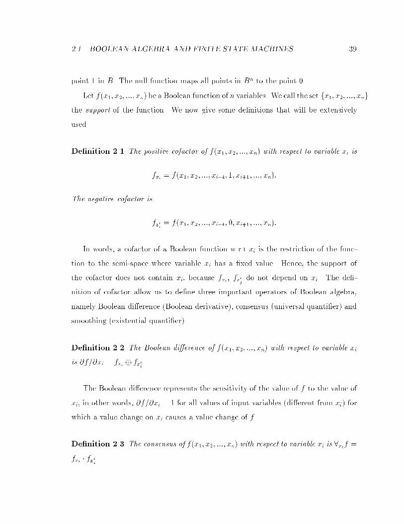
2.1. BOOLEAN ALGEBRA AND FINITE STATE MACHINES 39
point 1 in B. The null function maps all points in Bn to the point 0.
Let f(x1; x2; :::; xn) be a Boolean function of n variables. We call the set fx1; x2; :::; xng
the support of the function. We now give some de�nitions that will be extensively
used.
De�nition 2.1 The positive cofactor of f(x1; x2; :::; xn) with respect to variable xi is
fxi = f(x1; x2; :::; xi�1; 1; xi+1; :::; xn):
The negative cofactor is
fx0
i= f(x1; x2; :::; xi�1; 0; xi+1; :::; xn):
In words, a cofactor of a Boolean function w.r.t xi is the restriction of the func-
tion to the semi-space where variable xi has a �xed value. Hence, the support of
the cofactor does not contain xi, because fxi, fx0
jdo not depend on xi. The de�-
nition of cofactor allow us to de�ne three important operators of Boolean algebra,
namely Boolean di�erence (Boolean derivative), consensus (universal quanti�er) and
smoothing (existential quanti�er).
De�nition 2.2 The Boolean di�erence of f(x1; x2; :::; xn) with respect to variable xi
is @f=@xi = fxi � fx0
i.
The Boolean di�erence represents the sensitivity of the value of f to the value of
xi, in other words, @f=@xi = 1 for all values of input variables (di�erent from xi) for
which a value change on xi causes a value change of f .
De�nition 2.3 The consensus of f(x1; x2; :::; xn) with respect to variable xi is 8xif =
fxi � fx0
i
40 CHAPTER 2. BACKGROUND
The consensus is a fundamental operator in Boolean algebra and will be often used
in this thesis. It represents the component of f whose value is independent of xi. In
other words, 8xif = 1 for all values of input variables (di�erent from xi) for which
f = 1 no matter what is the value of xi. We will often call consensus the universal
quanti�er with respect to xi, because it represents conditions that make f = 1 for all
values of xi
De�nition 2.4 The smoothing of f(x1; x2; :::; xn) with respect to variable xi is 9xif =
fxi + fx0
i.
The smoothing is the dual of the consensus: 9xif = 0 for all values of input
variable (di�erent from xi) for which f = 0 no matter what the value of xi is. The
smoothing is often called existential quanti�er.
The greater or equal relation between two Boolean functions f � g holds if and
only if f � g0 = 1. An equivalent notation is g ) f . The de�nition given so far will
be clari�ed through an example.
Example 2.1.1. Consider the Boolean function f(a; b; c) = ab+ b0c+ a0b0c0.
The positive cofactor w.r.t c is fc = f(a; b; 1) = ab + b01 + a0b00 = ab + b0.
The negative cofactor is fc0 = f(a; b; 0) = ab + b00 + a0b01 = ab + a0b0. The
partial derivative is @f=@c = fc�f 0
c = (ab+b0)� (ab+a0b0) = ab0 The universal
quanti�er is 8cf = fcf0
c = (ab+b0) �(ab+a0b0) = ab+a0b0. Finally, the existential
quanti�er is 9cf = fc + f 0
c = (ab + b0) + (ab+ a0b0) = ab+ b0. Notice that all
operations involving cofactors reduce the support of the function by eliminating
the variable with respect to which the cofactors are taken. As an example of �
relation, observe that 9cf � 8cf (this is actually true for any Boolean function
f). 2
Boolean functions can be represented as sets (there is an isomorphism between set
algebra and binary Boolean algebra). We will sometimes adopt the set representation,
because it helps clarifying some concepts. A minterm is a point in the n-dimensional
Boolean domain of a Boolean function where the function has value 1. Thus, a

2.1. BOOLEAN ALGEBRA AND FINITE STATE MACHINES 41
a
b c
000 100
101
010 110111011
001
abc
00 01 11 10
0
1
1
1 1
1
1
a b c
1 1 −− 0 10 0 0
(a) (b) (c)
0
0
0
Figure 6: Pictorial representations of a Boolean Function
completely speci�ed Boolean function can be represented by the set of its minterms
(i.e. on set). An incompletely speci�ed Boolean function is de�ned by two sets (either
on set and o� set, or on set and don't care set, or o� set and don't care set).
Any Boolean function can be represented as a sum of products (SOP) of literals,
or as a product of sums of literals. A product of literals is often called a cube. One
particular sum of product representation is the minterm canonical form, where each
product has n literals. Each product in the minterm canonical form is a minterm of
the function. This representation is unique for any given function.
Example 2.1.2. Refer to function f of Example 1. f = ab + b0c + a0b0c0
is a sum of product representation, but so is f = abc + abc0 + b0c + a0b0c0.
Hence, there are many SOP representations for a single Boolean function. The
minterm canonical form of f is: f = abc+abc0+ab0c+a0b0c+a0b0c0. The function
has �ve minterms. Figure 6 shows three equivalent graphical representations of
f . In Figure 6 (a), the three-dimensional cube represents B3 and the darkened
vertices are the on set of f . In Figure 6 (b), the Karnaugh map of the function
is shown [mccl86]. Finally, Figure 6 (c) shows the representation of the function
as a list of cubes: the ones, represent positive literals, the zeros negative literals
and the \�" literals that do not appear in the product. For instance, ab0! 10�
and ab0c0! 100. 2
Several important de�nitions and concepts are related to the SOP representation
of Boolean functions.
De�nition 2.5 An implicant of a Boolean function f is a product of literals such
that f � p.

42 CHAPTER 2. BACKGROUND
Any product in a SOP representation is obviously an implicant of f . Particular
relevance has the concept of prime implicant.
De�nition 2.6 A prime implicant of f is an implicant of f is not contained in any
other implicant.
To better understand the de�nition, notice that a product in a SOP represents
a set of minterms. If we drop a literal from a product we expand the product (i.e.
we increase the number of minterms it contains by a factor of 2). A prime implicant
is a product that cannot be expanded. If we expand a prime implicant, some of
its minterm will not be contained in the on set of f . Thus, the product is not an
implicant any more.
De�nition 2.7 A cover of a Boolean function is a set (list) of implicants that covers
all its minterms
Any SOP representation of a Boolean function is a cover. A minimum cover is a
cover of minimum cardinality. The concept of minimum cover is important because
there is correlation between the number of implicants in a cover of a function (and
the number of literals in a cover) and the area of the hardware implementation of the
function [dmc94, mccl86]. Numerous algorithms for the minimization of covers have
been developed in the recent past (the book by De Micheli [dmc94] contains a good
overview). All these algorithms are based on a the following theorem:
Theorem 2.1 [Quine theorem]. There is a minimum cover that is prime.
The most important implication of this theorem is that it de�nes the search space
where a minimum cover can be found. If we restrict our search to covers formed by
prime implicants only, we are guaranteed to �nd a minimum cover. Although the
number of prime implicants can be exponential in the number of inputs of a Boolean

2.1. BOOLEAN ALGEBRA AND FINITE STATE MACHINES 43
function, several e�cient algorithms for SOP minimization based on Quine theorem
have been developed and successfully applied in industrial-strength CAD tools.
Boolean algebra provides a convenient framework for reasoning about properties
of digital circuits. In particular, the steady-state input-output behavior of a feedback-
free digital circuits (a.k.a. combinational circuits) can be modeled by a multi-output
Boolean function. Large combinational circuits are often better described in a struc-
tural fashion by logic networks (also called combinational networks). A logic network is
an interconnection of modules, representing input/output ports, logic gates or single-
output logic functions. The logic network can be represented as a directed acyclic
graph (DAG), with vertices corresponding to the modules and edges corresponding
to two-terminal nets to which the original module interconnects are reduced.
Notice that a circuit behavior (i.e. a multiple output Boolean function) can be
mapped to many equivalent structures. The lack of uniqueness is the main limita-
tion of the the structural description. Given two circuit descriptions, checking their
equivalence is not an easy task. On the other hand, there are Boolean function for
which all known abstract descriptions have unmanageable size. For such functions, a
structural representation is the only viable alternative. Moreover, structural descrip-
tions are conceptually closer to the physical implementation, and are widely used for
simulation and performance analysis.
2.1.2 Finite state machines
We formally de�ne a �nite state machine with binary inputs and outputs as a 6-tuple
(X;Z; S; s0; �; �), where X = Bn is the input space, Z = Bm the output space, S is a
�nite set of states, s0 is the initial (reset) state, �(x; s) : X �S ! S is the next state
function and �(x; s) : X � S ! Z is the output function. FSMs are categorized in
two classes [hart66, henn68, koha70]:

44 CHAPTER 2. BACKGROUND
S1 S2
S0
−1/−010/00
−1/0110/01
00/01
00/10 10/1001/−1
11/11
00/00
(a)
S0 −1 S0 −0S0 10 S0 00S0 00 S1 01S1 −1 S1 01S1 10 S1 01S1 00 S2 10S2 10 S2 10S2 01 S2 −1S2 11 S1 11S2 00 S0 00
PS In NS O
(b)(a)
Figure 7: State transition graph and state table of a FSM
De�nition 2.8 A Moore machine is a FSM where �(x; s) = �(�; s), i.e. the outputs
do not depend directly on the input value, but the depend only on the state. A Mealy
machine is a FSM for which this property does not hold.
Finite-state machines can be incompletely speci�ed. An incompletely speci�ed
FSM is one where �(x; s) and/or �(x; s) are incompletely speci�ed Boolean functions.
Notice that in the de�nition of FSM, the state set S is not de�ned as a Boolean
space. In other words, the states are elements of a generic set, and they are uniquely
identi�ed by a symbol (a string or any other unique identi�er). A FSM can be
represented by a graph or, equivalently by a table. The two representations ale called
state transition graph (STG) and state transition table (or state table, for brevity),
respectively. The states of the STG are labeled with the unique symbolic state name,
the edges are labeled with the inputs and output values. The state table is simply
the list of edges of the STG. An example will better illustrate these de�nitions.
Example 2.1.3. Consider the FSM in Figure 7 (a), (b). Part (a) shows the
STG of the FSM, while Part (b) shows the state table. The notation used in
the STG for edge labeling is that the inputs are followed by the outputs. Each
edge in the STG correspond to an entry in the state table. The �st two �elds in
the state table are respectively present state and input. The last two �elds are
next state and output. The FSM of Figure 7 is incompletely speci�ed, because
for present state S2 and input 01 the �rst output is not speci�ed (i.e. it can be

2.1. BOOLEAN ALGEBRA AND FINITE STATE MACHINES 45
either one or zero). The output is incompletely speci�ed for the �rst transition
in the table as well. 2
Notice that both STG and state table completely de�ne the input-output behavior
of a FSM, but they do not provide any information about the circuit implementation.
Hence, STG and state table are behavioral representations of the FSM. In order to
obtain a representation which is closer the the circuit implementation, we need to
introduce the concept of state-encoding.
De�nition 2.9 A state encoding is a one-to-one mapping from S to BNs, a function
E : S ! BNs. Ns is the number of state variables.
By specifying the state encoding function E, we associate each symbolic state
to a particular binary vector of Ns elements, i.e. to a vertex in the Ns-dimensional
Boolean space. The vertex is called state code. Notice that we have numerous degrees
of freedom in the choice if E. The only important constraint for E is that BNs has
enough vertices to assign a di�erent one to each symbolic state, thus Ns � dlog2jSje.
Once we have speci�ed Ns and E, the state of a FSM is completely expressed by Ns
binary variables called state variables.
If we specify E, the output and next state functions become Boolean functions:
�(x; v) : Bn�BNs ! BNs, �(x; v) : Bn�BNs ! Bm, where v = E(s). If the number
of elements in BNs is larger than jSj, both �(x; v) and �(x; v) become incompletely
speci�ed, since their value is not relevant for values of v that do not correspond to
any valid state. For the sake of brevity, we will often use the notation �(x; s) and
�(x; s) even for FSM where E has been speci�ed, with the convention that s is the
state code of the symbolic state.
Once the state encoding has been speci�ed, the structural model of FSM shown
in Figure 8 can be used to represent the FSM. A (combinational) logic network
implements � and �, while state elements ( ip- ops) store the value of one state

46 CHAPTER 2. BACKGROUND
CLK
X Z
S
Combinational Logic
Figure 8: Structural representation of a FSM
variable. The structural model is called sequential or synchronous network. We
assume that the ip- ops are triggered on the raising edge of the clock CLK (the
triangular shape within each ip- op symbol identi�es the ip- ops as positive-edge-
triggered). Numerous types of sequential elements and clocking styles can be used to
implement real-life circuits, but it is useful to reason about a single implementation
model.
The representation of Figure 8 is structural, because it refers to a particular circuit
structure implementing the FSM. Notice that there are in�nite structural represen-
tations for a single STG (they can be generated by changing Ns and E). The main
reason why structural representations are useful even when developing algorithm or
studying properties of FSMs is that they may be much more compact than the state-
based representations.
Example 2.1.4. Consider a FSM with ten millions of states. If we represent
each symbolic state with a string of characters from an alphabet with 32 sym-
bols, we need at least 4 characters (minimum length identi�ers) for each state.
We want to estimate the memory needed to store the behavioral representation

2.1. BOOLEAN ALGEBRA AND FINITE STATE MACHINES 47
of the FSM. Only storing the names of the states requires 106 �4�5=8 � 25Mb.
In contrast, the minimum number of state variables needed to uniquely rep-
resent all states is Ns = dlog2107e = 21. Just 21 ip- ops are su�cient for
encoding the 107 states. In other words, the STG of a relatively small sequen-
tial circuit with 21 ip- ops may already be unmanageably large. 2
Although it is often convenient to reason about small-size sequential system using
behavioral representations, structural representations are the only viable alternative
for large sequential systems. Similarly to the case of combinational network, the
main limitation of the sequential network representation is its lack of uniqueness.
Additionally, checking the equivalence of two sequential networks is at least as hard
as checking the equivalence of their combinational part.
2.1.3 Discrete functions
We have introduced the concept of Boolean functions and we showed how FSMs can
be represented by Boolean functions. We now present a simple extension of Boolean
functions.
De�nition 2.10 A discrete function f : Bn ! V is a mapping from a Boolean space
to a �nite set V .
Discrete functions encompass Boolean functions as a particular case. When V =
B = f1; 0g, a discrete function is Boolean. Notice however that discrete functions are
not more expressive than Boolean functions: since set V is �nite, we can \encode"
it with Ne = dlog2jV je binary variable. Thus a generic discrete function f can be
represented by a multi-output Boolean function and an encoding function. Despite
this fact, discrete functions are an useful abstraction that will be employed in the
development of algorithms for power minimization.

48 CHAPTER 2. BACKGROUND
2.2 Implicit representation of discrete functions
Digital circuits may have unmanageably large abstract representations. The reason is
that both Boolean functions and FSMs can be represented in tabular format, but the
size of the tables is worst-case exponential in the number of inputs (and states, in the
case of FSMs). One approach that mitigates this problem is to resort to structural
representations. The main limit of structural representations is that they are not
unique. A Boolean function can be represented by an in�nite number of combinational
networks, and a FSM can be represented by in�nite sequential networks. Hence, it is
hard to develop algorithms based on the properties of a Boolean function or a FSM
when starting from a structural representation.
In this section we will describe a powerful data structure that allows the repre-
sentation of Boolean functions and state machines in a canonical fashion (i.e. with
a unique representation) which has in many cases manageable size, even when the
tabular representation is excessively large.
2.2.1 Binary decision diagrams
Binary decision diagrams (BDDs) are a data structure developed for the compact
representation of large Boolean functions. Several variants of BDDs have been devel-
oped by di�erent groups of researchers (see, for instance, [brya86, brac90, madr88,
mina90]). The di�erences are generally small. In our description we will follow [brya86]
and [brac90], though with slightly di�erent notation. We introduce the keys concept
of the BDD representation by means of a simple example
Example 2.2.5.
Let us consider the following Boolean function:
f = abc+ b0d+ c0d:
A BDD for this function is given in Figure 9.

2.2. IMPLICIT REPRESENTATION OF DISCRETE FUNCTIONS 49
a
b
c
b
c
d
1 0
T E
T E ET
TE E
T
T E
f
Figure 9: A Binary Decision Diagram.
If we want to know the value of f for a particular assignment to the variables a,b, c, and d, we just follow the corresponding path from the square box labeledf (this node is the root of the BDD) to one of the square boxes labeled 1 and0 (these nodes are the leaves of the BDD). Suppose we want to determine thevalue of function f for the assignment a = 1, b = 0, c = 1, and d = 0. The�rst variable encountered from the root is a, whose value is 1. We then followthe arc labeled T (which stands for then). We then come across a node labeledb. Since the value of b is 0, we follow the arc labeled E (else). The next nodeis labeled d, which implies that for a = 1 and b = 0, the value of f does notdepend on c. Following the E arc we �nally reach the leaf labeled 0. This tellsus that the value of the function is 0, as can be easily veri�ed from the sum ofproducts formula.
The BDD of Figure 9 is an ordered binary decision diagram, because the vari-ables appear in the same order along all paths from the root to the leaves. Theordering in this case is
a � b � c � d:
The appearance and the size of the BDD depend on the variable ordering. Thisis illustrated in Figure 10, where a di�erent BDD for f is given according tothe following variable ordering:
b � c � a � d;

50 CHAPTER 2. BACKGROUND
1 0
T E
T E
T
ET
E
b
c
a
d
f
Figure 10: An Optimal BDD.
This is an optimal ordering, since there is exactly one node for each variable.
We will assume that BDDs are ordered. 2
The BDD of f constructed as shown in the example may not be reduced, that is,
it may contain duplicated and super uous nodes. However, a non-reduced BDD can
be systematically transformed into a reduced one by iteratively applying:
� Identi�cation of isomorphic sub-graphs;
� Removal of redundant nodes.
Given an ordering, the reduced graph for a function is unique. Hence, the Reduced
Ordered BDD (ROBDD) is a canonical form, that is, two functions f1 and f2 are
equivalent (i.e., f1 = f2) if and only if they have the same BDD. This is the �rst
important characteristics of binary decision diagrams. Other interesting properties of
BDDs are:
� The size of the BDD (the number of nodes) is exponential in the number of
variables in the worst case; however, BDDs are well-behaved for many functions

2.2. IMPLICIT REPRESENTATION OF DISCRETE FUNCTIONS 51
that are not amenable to tabular representations (e.g., EXCLUSIVE-OR).
� The logical AND and OR of BDDs have the same complexity (polynomial in
the size of the operands). Complementation is inexpensive (constant time).
� Both satis�ability (i.e. proving that a Boolean function has at least one satis-
fying assignment) and tautology (i.e. proving that a Boolean function is always
1) can be solved in constant time. Indeed, f if satis�able if and only if its BDD
is not the terminal node 0, it is a tautology if and only if its BDD consists of
the terminal node 1.
On the other side, BDDs have some drawbacks:
� BDD sizes depend on the ordering. Finding a good ordering is not always
simple.
� There are functions for which the sum of products or product of sums represen-
tations are more compact than the BDDs.
� In some cases sum of products/product of sums forms are closer to the �nal
implementation of a circuit. For instance, if we want to implement a PLA, we
need to generate at some point a sum of products or product of sums form.
BDDs allow to compactly store and manipulated multiple Boolean function, since
it is possible to share nodes in the BDD representations of two or more Boolean
functions. As a limit case, notice that two equivalent functions fully share all nodes,
i.e. they are represented by the same BDD (not just two identical BDDs).
Given that we are interested in reduced BDDs, instead of generating non-reduced
BDDs and then reducing them, we guarantee that, at any time, there are no iso-
morphic sub-graphs and no redundant nodes in the multi-rooted DAG. This can be
achieved by checking for the existence of a node representing the function we want to

52 CHAPTER 2. BACKGROUND
add, prior to the creation of a new node. A straightforward approach would consist
of searching the whole DAG every time we want to insert a new node. However, that
would be far too ine�cient. Instead, a hash table called unique table is created. The
unique table contains all functions represented in the DAG. In other words, the table
has one unique entry for each node.
BDDs are manipulated with recursive algorithms based on the cofactor expansion
of Boolean functions f with respect to a variable:
f = xi � fxi + x0ifx0
i: (2.9)
The usefulness of Equation 2.9 lies in the fact that after cofactor expansions, the
two cofactors fxi and fx0
iare simpler functions. All Boolean operations de�ned in
Section 2.1 can be e�ciently carried out on the BDDs representing the functions on
which they apply. The complexity of the computations is polynomial in the number
of BDD nodes of the functions (more precisely, linear in the product of the number
of BDD nodes of each operand).
BDD manipulation packages keep a cache of recently computed functions, called
computed table, for e�ciency reasons. The purpose of this table is di�erent from that
of the unique table. With the unique table we answer questions like: \Does there
exist a node labeled v with children g and h?" On the other hand, the computed table
answers questions like: \Did we recently compute the AND of f1 and f2?" We can
ask this question before we actually know that the AND of f1 and f2 is a function
whose top node is labeled v and whose children are g and h. Hence we can avoid
recomputing the result.
2.2.2 Algebraic decision diagrams
Since discrete functions are a straightforward extension of Boolean functions, the
intuition suggests that data structures similar to BDDs could be used to e�ciently

2.2. IMPLICIT REPRESENTATION OF DISCRETE FUNCTIONS 53
manipulate them. Indeed, several \BDD-like" data structures have been developed
to this purpose [clar93, lai94, baha95]. The one we adopt is the algebraic decision
diagram (ADD) [baha95]. We do not describe the de�nition and the properties of
ADDs since they are analogous the the ones we illustrated for BDDs: reduced and
ordered ADDs are a canonical representation of discrete functions and all important
operations with ADDs can be performed in polynomial time in the ADD size.
The main di�erence between BDDs and ADDs is in the terminal nodes. While
all BDDs terminate in either the \0" or the \1" terminal nodes, ADDs have multi-
ple terminal nodes. The terminal nodes (leaves) of an ADD are associated with the
values of the discrete function it represents. Since operators on discrete functions
are generalizations of Boolean operators, the ADD algorithms that implement such
operators are very similar to the procedures used for BDDs. We review three im-
portant operators on ADDs that will be used in later chapters: ITE, APPLY, and
ABSTRACT.
ITE takes three arguments: f , an ADD restricted to have only 0 or 1 as terminal
values (called \0/1-ADD", and fully equivalent to a BDD), and g and h, generic
ADDs. It is de�ned by:
ITE(f; g; h) = f � g + f 0 � h (2.10)
Intuitively, the resulting ADD has the same leaves as g when f is 1 and the leaves of
h when f is zero.
APPLY takes one operator, op (e.g., +, �, �), and two operand ADDs as argu-
ments; it applies op to all corresponding elements of the two operands and returns the
resulting ADD. Notice that APPLY generalizes the Boolean operators. For example,
the APPLY of � (multiplication) to two 0/1-ADDs degenerates to the Boolean AND
operator.

54 CHAPTER 2. BACKGROUND
A B C f(A, B, C)
0 0 0 50 0 1 50 1 0 30 1 1 51 0 0 31 0 1 51 1 0 31 1 1 1 1 3 5
T E
ET T E
TET E
A
B B
C C
(b)
T E
ET T
A
B B
4 8 10
E
(c)(a)
f
\ f+c
Figure 11: (a)-(b) A discrete function f and its ADD. (c) The ABSTRACT of f w.r.tc, n+c f .
ABSTRACT reduces the dimensionality of its argument function through exis-
tential arithmetic abstraction of some variables. Let x; y be the support of a pseudo-
Boolean function f(x; y), where x and y be two disjoint sub-sets of Boolean variables.
The arithmetic existential abstraction of x from f(x; y) with respect to the arithmetic
sum is de�ned as:
n+x f(x; y) =
Xx
f(x; y): (2.11)
This de�nition tells that, instead of taking the Boolean sum of all the the cofactors
associated with the minterms of the x-variables, as in Boolean existential abstraction,
the ABSTRACT operator computes precisely the arithmetic sum. Notice that the
ABSTRACT operator eliminates x from the support (i.e n+x f(x; y) = g(y)). Similarly,
the arithmetic existential abstraction of x with respect to theMAX operator is de�ned
as:
nMAXx f(u) = maxx
f(u): (2.12)
Example 2.2.6. A discrete function f is given in tabular form in Fig-
ure 11 (a). The ADD of the function is shown in Figure 11 (b), with the

2.3. MARKOV ANALYSIS OF FINITE STATE MACHINES 55
variable order a � b � c. The arithmetic existential abstraction of f with re-
spect to variable c is shown in Figure 11 (c). As expected, n+c f does not depend
on c any more. 2
2.3 Markov analysis of �nite state machines
Power is a strongly pattern-dependent cost function, since it depends on the switching
activity of a circuit, which in turn depends on the input patterns applied to the circuit.
Hence, we need to specify some information about the typical input patterns applied
to a circuit if we want to optimize or even only estimate its power dissipation. The
most straightforward way to provide information about input patterns is to actually
provide a long input stream representing a typical usage pattern together with the
speci�cation of the circuit.
This approach gives the most complete information, but it su�ers from two serious
drawbacks i) the input traces can be very large and cumbersome to manage, ii) in
many cases only incomplete information about the environment may be available.
A more synthetic description of the input streams can be provided by providing
information about input probabilities. Given a sequential circuit, we may simply
provide one real number for each input: the probability for the input to be one. This
statistical parameter is called signal probability.
Obviously, signal probabilities express much less information than a complete in-
put trace, for example they do not give any indication about correlation between suc-
cessive input values (called temporal correlations) or between di�erent inputs (called
spatial correlations). Nevertheless, input probabilities are often used to synthetically
describe the statistics of the input patterns.
Even if we assume that the input patterns can be described by signal probabilities
with su�cient accuracy (i.e. spatio-temporal correlations are a second-order e�ect),
it is not obvious how to estimate, in a FSM, the probability of a state transition, since

56 CHAPTER 2. BACKGROUND
it depends not only on the inputs, but also on the state information. For example, if
an FSM has a transition from state si to state sj for all possible input con�gurations,
we may think that this transition will happen with very high probability during the
operation of the machine. This may not be the case: if state si is unreachable,
the machine will never perform the transition, because it will never be in state si.
Similarly, if the probability of being in state si is very low, a transition from state si
to state sj is very unlikely.
We model the stochastic behavior or a FSM by a Markov chain. A Markov chain is
a representation of a �nite state Markov process [triv82], a stochastic model where the
transition probability distributions at any time depend only on the present state and
not on how the process arrived in that state. The Markov chain model for the STG
is a directed graph isomorphic to the STG and with weighted edges. For a transition
from state si to state sj , the weight pi;j on the corresponding edge represents the
conditional probability of the transition (i.e., the probability of a transition to state
sj given that the machine was in state si). Symbolically this can be expressed as:
pi;j = Prob(Next = sjjPresent = si) (2.13)
Note that edges with zero conditional probability are never drawn in the graph
representation of the Markov chain.
De�nition 2.11 The conditional probability distribution is the set of pi;j values.
The conditional probability distribution is external input information. It does
not depend on the structure of the Markov chain and we assume that it is known.
Although conditional transition probabilities can be used as a rough approximation
to the transition probabilities [roy93], we need to know the probability of a transition
independent of the present state. These probabilities are called total transition prob-
abilities, Pi;j, and can be calculated [triv82] from the state probabilities, where the
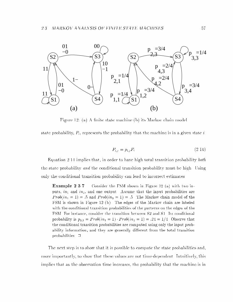
2.3. MARKOV ANALYSIS OF FINITE STATE MACHINES 57
S2
S1 S4
S3
0−
10−1
0001−0
1−
11
01−0
11
S2
S1 S4
S3
p =1/42,1
p =1/41,1
p2,3
=3/4
p1,2
=3/4
p4,2
=2/4
p =2/44,3
p3,3
=1/4
p3,4
=3/4
(a) (b)
Figure 12: (a) A �nite state machine (b) its Markov chain model
state probability, Pi, represents the probability that the machine is in a given state i.
Pi;j = pi;jPi (2.14)
Equation 2.14 implies that, in order to have high total transition probability both
the state probability and the conditional transition probability must be high. Using
only the conditional transition probability can lead to incorrect estimates.
Example 2.3.7. Consider the FSM shown in Figure 12 (a) with two in-
puts, in1 and in2, and one output. Assume that the input probabilities are
Prob(in1 = 1) = :5 and Prob(in2 = 1) = :5. The Markov chain model of the
FSM is shown in Figure 12 (b). The edges of the Markov chain are labeled
with the conditional transition probabilities of the patterns on the edges of the
FSM. For instance, consider the transition between S2 and S1. Its conditional
probability is p2;1 = Prob(in1 = 1) � Prob(in2 = 1) = :24 = 1=4. Observe that
the conditional transition probabilities are computed using only the input prob-
ability information, and they are generally di�erent from the total transition
probabilities. 2
The next step is to show that it is possible to compute the state probabilities and,
more importantly, to show that these values are not time-dependent. Intuitively, this
implies that as the observation time increases, the probability that the machine is in

58 CHAPTER 2. BACKGROUND
each of its states converges to a constant (stationary) set of real numbers. In other
words, we must show that it is possible to compute a steady state (or stationary)
probability vector whose elements are the stationary state probabilities.
It is quite easy to �nd STGs for which the stationary state probabilities do not
exist, because, for example, their value is oscillatory. The general theory explaining
the asymptotic behavior of the state probabilities is too involved to be described here,
but it can be found in reference [triv82]. Here we just state an an important theorem
that allows us de�ne a large class of STGs whose corresponding Markov chains have
a steady state probability vector.
Theorem 2.2 For an irreducible, aperiodic Markov chain, with all states recurrent
non-null, the steady state probability vector exists and it is unique
An irreducible Markov chain with all the states recurrent non null is a chain where
every state can be reached from any other state, and the greatest common divisor
of the length of the possible closed paths from every state is one. For the sake of
simplicity, we assume in the following that we deal only with FSMs for which the
corresponding Markov chain satis�es all requirements of Theorem 2.2 for existence
and uniqueness of the state probability vector. We will prove in a later chapter that
the presence of a unique reset state is su�cient to ensure the existence of the steady
state probability vector. Notice however that state probabilities can be computed in
much more relaxed assumptions than those of Theorem 2.2 even for FSMs without a
unique reset state [hama94].
In the next subsections we describe the basic methods for computation of the state
probability vector i) for small-size FSMs that can be described in a behavioral style,
ii) for large FSMs described in a structural fashion.

2.3. MARKOV ANALYSIS OF FINITE STATE MACHINES 59
2.3.1 Explicit methods
The methods for computation of the state probability vector presented in this sub-
section are called explicit because they are based on the direct representation of the
conditional transition probabilities with a matrix of size jSj � jSj. Let P be the con-
ditional transition probability matrix whose entries pi;j are the conditional transition
probabilities, and q the steady state probability vector whose components are the
state probabilities Pi (i.e q = [P1; P2; :::; PjSj]T ). Then we can compute the steady
state probabilities by solving the (ns + 1) system of equations:
qT P = qT (2.15)nsXi=1
Pi = 1 (2.16)
The problem of �nding the steady state probability vector is thus reduced to �nd-
ing the left eigenvector of the transition matrix corresponding to the unit eigenvalue,
and normalizing it in order to make the sum of its elements equal to unity [triv82].
The normalization condition (Equation 2.16) is required because matrix P is singular
(since all its columns sum to one), and the Equation 2.15 has in�nite solutions. The
only valid solution is found by imposing that the sum of all the components of q
is one, because the elements of q are probabilities of mutually exclusive events that
cover the complete event space (i.e. the Markov chain is always in one and only one
of its states).
Example 2.3.8. For the Markov chain of Example 7, the stationary state
probabilities calculated solving Equation 2.15 are shown in Figure 13 besides
the nodes in the chain. Obviously, the state probabilities sum to one, as en-
forced by the normalization condition. The �gure shows also the total transi-
tion probabilities (the products pi;j � Pj) on the edges. Notice that the total
transition probabilities are completely di�erent from the conditional transition
probabilities: while all conditional transition probabilities leaving a state sum
to one, the sum of all total transition probabilities is one. 2

60 CHAPTER 2. BACKGROUND
S1 S4
S3
9/58
9/58
3/58
3/58
9/589/29
3P =12/29
P =9/29P =2/29
P =6/292
1 41/58
3/29
S2
Figure 13: Stationary state probabilities and total transition probabilities
For sparse and large conditional transition probability matrices, the solution of
System 2.15 can be carried out using iterative methods that do not require matrix
inversion. One iterative method that is very simple and well-suited for state proba-
bility computations is the power method. With this approach, the state probability
vector q can be computed using the iteration:
qTn+1 = qTn P (2.17)
with the normalization conditionPjSj
i=1 Pi = 1 until convergence is reached. The
convergence properties of this method are discussed in [hama94]. The main advan-
tage of the power method is that it can leverage well-developed techniques for the
manipulation of large matrices for which the computation of matrix by vector product
has complexity proportional to the number of nonzero elements of P.
The main limitation of the methods presented in this section is that they are not
applicable to Markov chains derived from large sequential circuits for which the state
set large enough to make even the storage of matrix P a formidable task.

2.3. MARKOV ANALYSIS OF FINITE STATE MACHINES 61
2.3.2 Implicit methods
When dealing with sequential circuits with thousands or even millions of states, spec-
i�ed by a structural description, it is very hard to extract and manipulate the tran-
sition probability matrix. Implicit methods allow the manipulation of large systems
by representing the transition probability matrix with an ADD.
The STG of a �nite state machine is implicitly represented by the BDD (or,
equivalently, by a 1/0-ADD) of its transition relation [coud89]. The transition relation
is a Boolean function T (x; s; ns) : BN�BNs�BNs ! B. The support of the transition
relation consists of: i) the input variables x, ii) the state variables s, iii) the next state
variables ns. T has value 1 when the STG of the machine has a transition from state
s to state ns with input x, zero otherwise.
The transition relation can be extracted directly from the next state function
�(x; s) with an iterative procedure of �xed point computation. Starting from an initial
state (e. g. the reset state of the machine), the set of states that can be reached from
it in one clock cycle is computed. The procedure then iterates computing all states
reachable from the set of states reached in the previous iterations. The iteration stops
a soon as no new states are reached in two successive iterations (i.e. a �xed point has
been reached).
The �xed point computation can be carried out by operating directly on BDDs.
The transition relation is computed without ever enumerating the states. BDD-based
algorithms for the computation of T (x; s; ns) have been able to completely explore the
state spaces of machines with more than 1020 states, for which any enumerative algo-
rithm would be completely impractical. The interested reader can refer to [some96]
for a review of BDD-based procedures for transition relation computation.
Similarly, the input probabilities can be represented by an ADD. The ADD PI(x)
is extracted from the array of input probabilities, with the simple formula PI(x) =Qmi=1 PIi(xi) where each PIi(xi) is a single-node ADD, with two leaves with value pi

62 CHAPTER 2. BACKGROUND
00 01 11 10
0
1 1 1
1 1
0
0
0
0
T
ns
E
EE
T
TT
s
EETT
1 0
nsT
0/1
0 1
0/0
1/11/0 (.2) (.8)(.2)
(.8)
PI
T E
.2 .8
P
(a) (b)
(c) (d) (e)
EETT
ET
.8 .2
s
x x x
s, x
Figure 14: Symbolic computation of the conditional transition probability matrix
and 1� pi.
Given T and PI, the implicit representation of matrix P can be obtained with
the following symbolic formula
P(x; s) = PI(x) � n+nsT (x; s; ns) (2.18)
Equation 2.18 produces an ADD with leaves the conditional input probabilities of
the transitions of the STG. Notice that the value of x and s are su�cient to identify
every transition in the STG. Notice that the ADD of P can be exponentially smaller
than the traditional matrix representation.
Example 2.3.9. The STG of a �nite state machine is given in Figure 14 (a).
Notice that each edge is labeled with input, output and conditional transition
probability. The transition relation T (x; s; ns) is shown in Figure 14 (b) in

2.4. SUMMARY 63
the tabular format. The BDD (0/1 ADD) of T is shown in Figure 14 (c).
The ADD of the conditional input probability is shown in Figure 14 (d). If we
compute the ADD of matrix P using Equation 2.18, we obtain the result shown
in Figure 14 (e). Although we used a small example for the sake of explanation,
notice that symbolic representation based on ADD becomes useful when the
STG and the truth table of T are unmanageably large. 2
Once P(x; s) has been computed, the state probability vectors can be computed
using the symbolic version of the power method. The matrix-by-vector multiplication
required for the application of the power method (Equation 2.17) is implemented as
an ADD operator, and the �nal result is q(s), the ADD whose leaves are the state
probabilities. Notice that other implicit methods have been presented in the work
by Macii et al. [hach94], as well as a detailed study of the convergence properties of
symbolic algorithm for the calculation of q in the case of large FSMs that do not
satisfy theorem 2.2.
2.4 Summary
In this chapter we covered the background material required for full understand-
ing of the power optimization algorithms presented in the following chapters. The
key concepts introduced so far are: Boolean and discrete functions, the quanti�-
cation operators, BDDs, ADDs and Markov models for �nite state machines. The
BDD/ADD-based symbolic representation of Boolean functions, FSMs and Markov
chains is a useful tool when dealing with systems with a large number of inputs and
state variables.

Chapter 3
Synthesis of gated-clock FSMs
3.1 Introduction
In synchronous circuits, it is possible to selectively stop the clock in portions of the
circuit where active computation is not being performed. As discussed in Chapter 1,
local clocks that are conditionally enabled are called gated clocks, because a signal
from the environment is used to qualify (gate) the global clock signal. Gated clocks
are commonly used by designers of large power-constrained systems [sues94, schu94]
as the core of dynamic power management schemes. Notice however that it is usually
responsibility of the designer to �nd the conditions that disable the clock.
We consider sequential systems described by �nite state machines and we target
the reduction of the useless switching activity as de�ned in Chapter 1. We move
from the observation that during the operation of a FSM there are conditions such
that the next state and the output do not change. Therefore, clocking the FSM
only wastes power in the combinational logic and in the registers. If we are able to
detect when the machine is idle, we can stop the clock until a useful transition must
be performed and the clocking must resume. The presence of a gated clock has a
two-fold advantage. First, when the clock is stopped, no power is consumed in the
64

3.1. INTRODUCTION 65
FSM combinational logic, because its inputs remain constant. Second, no power is
consumed in the sequential elements ( ip- ops) and the gated clock line.
Obviously, detecting idle conditions requires some computation to be performed by
additional circuitry. This computation dissipates power and requires time. Sometimes
it will be too expensive to detect all idle conditions. It is therefore very important
to select a subset of all idle conditions that are taken with high probability during
the operation of the FSM. We will show that idle conditions correspond to self-loops
of Moore FSMs, and therefore it is relatively easy to detect them. Idle conditions in
Mealy FSMs can also be detected, but with more e�ort.
We address the synthesis of the clock-stopping logic. More in detail, we formulate
and solve a new logic synthesis problem, namely the choice of a minimum-complexity
sub-function Fa of a given Boolean function fa, such that its probability of being
true is larger than a prede�ned fraction of the total probability of fa. This is the
main theoretical result in this chapter, and it is applicable to a variety of dynamic
power management schemes, such as precomputation or guarded evaluation. From a
practical point of view, our algorithm chooses a subset of all idle conditions such that
the clock-stopping circuitry dissipates minimum power but stops the clock with high
e�ciency.
Experimental results will be presented for a number of benchmark circuits speci�ed
by state tables. Since state table speci�cations are suitable only for small sequential
systems, the largest example we present has a few hundreds of states. One observation
that could be made is that controllers speci�ed as state table are responsible for a
small fraction of the total power dissipation of a chip, therefore the impact of our
technique is likely to be small. It is however important to notice that small FSMs
control large data-paths and idle conditions for the controller are often idle for the
data-path as well. Thus, detecting idle conditions on the controller leads to detecting
(and exploiting) idle conditions for the controlled data-path, obtaining much larger

66 CHAPTER 3. SYNTHESIS OF GATED-CLOCK FSMS
power savings. Moreover, in Chapter 4 we will introduce symbolic techniques that
drastically enlarge the spectrum of applicability of automatic gated clock generation
to sequential systems for which the behavioral description is unacceptably large.
We embedded our tool in a complete synthesis path from state-table speci�ca-
tion to transistor-level implementation and we employed accurate switch-level simu-
lation [salz89] to verify our results, because gate-level power estimation has limited
accuracy. Since the clock-gating logic may add its delay to the critical path, particu-
lar care must be taken in detecting and eliminating timing violations that may arise
when the cycle time closely matches the critical path of the original FSM. For some
circuits more than 50% reduction in average power dissipation has been obtained,
but quality of the results is strongly dependent on the type of �nite-state machine we
start with. In particular, our method is well suited for FSMs that behave as reactive
systems: they wait for some input event to occur and they produce a response, but for
a large fraction of the total time they are idle. Practical examples of such machines
can be found for instance in portable devices such as pagers which are typical reactive
systems, and for which power minimization in important.
The rest of the chapter is organized as follows. In Section 3.2 we describe the
architecture of the gated-clock FSM and we discuss the detailed timing of the signals
that control the clock. In Section 3.3 we formulate the problem of �nding idle condi-
tions for a FSM and we introduce a novel transformation that enables the extraction
of such condition. Section 3.4 is dedicated to algorithms for the synthesis and op-
timization of the clock-stopping logic. Section 3.5 describes implementation details,
experimental setting and results. Finally, in Section 3.6 we draw some conclusions.

3.2. GATED-CLOCK FSMS 67
3.2 Gated-clock FSMs
We will assume hereafter a single clock scheme with edge-triggered ip- ops, shown
in Figure 15 (a). This is not a limiting assumption. We have indeed applied our
methods to di�erent clocking schemes in [beni94a] (where we used transparent latches
and multi-phase clocks). The FSM model of Figure 15 (a) is di�erent from the generic
FSM structure we described in Chapter 2, where the primary inputs are not latched.
The FSM structure without latched inputs is seldom used in the design practice. In a
large system, control logic and data-path are always decomposed in interacting sub-
units, for obvious reasons of complexitymanagement. The interface between sub-units
(interacting FSMs in our case) is usually composed by sequential elements [west92] (in
our case, D- ip- ops). If such boundary does not exist, there is a combinational path
between adjacent sub-units. This is seldom allowed in industrial design methodologies
(it makes timing analysis harder and increases the risk of timing violations). Even if
we consider a design that is simple enough to be described by a single FSM, ip- ops
are usually inserted on the inputs to obtain better signal quality and synchronization.
From a more theoretical point of view, the FSM with latched inputs di�ers from
the FSM without input latches because the outputs in the �rst model lag the outputs
by one clock cycle. The input-output behavior of the two models is therefore equiva-
lent modulo a translation in time of the output stream (assuming that the ip- op on
the inputs are reset at the same values taken in the �rst clock cycle by the primary
inputs of the machine without input ip- ops).
A gated clock FSM is obtained modifying the structure in Figure 15 (a). We
de�ne a new signal called activation function (fa) whose purpose is to selectively
stop the local clock of the FSM, when the machine does not perform state or output
transitions. When fa = 1 the clock will be stopped. The modi�ed structure is shown
in Figure 15 (b). The block labeled \L" represents a latch, transparent when the

68 CHAPTER 3. SYNTHESIS OF GATED-CLOCK FSMS
Combinational Logic
IN OUT
STATE
GCLK
CLK
&LaF
Combinational Logic
OUT
STATE
CLK
IN
(a) (b)
Figure 15: (a) Single clock, ip- op based �nite-state machine. (b) Gated clock
version.
global clock signal CLK is low. Notice that the presence of the latch is needed for a
correct behavior, because fa may have glitches that must not propagate to the AND
gate when the global clock is high. Moreover, notice that the delay of the logic for
the computation of fa is on the critical path of the circuit, and its e�ect must be
taken into account during timing veri�cation.
The modi�ed circuit operates as follows. We assume that the activation function
fa becomes valid before the raising edge of the global clock. At this time the clock
signal is low and the latch L is transparent. If the fa signal becomes high, the
upcoming edge of the global clock will not �lter through the AND gate and therefore
the FSM will not be clocked and GCLK will remain low. Note that when the global
clock is high, the latch is not transparent and the inverted input of the AND gate
cannot change at least up to the next falling edge of the global clock.
The activation function is a combinational logic block with inputs the primary
input IN and the state lines STATE of the FSM. No external information is used, the
only input data for our algorithm is the behavioral description of the FSM and the
probability distribution of the input signals.

3.2. GATED-CLOCK FSMS 69
fa
CLK
GCLK
CLK
GCLK
fa
(b)(a)
Figure 16: Timing diagrams of the activation function fa, the global clock CLK and
the gated clock GCLK when (a) a simple AND gate is used, (b) a latch and the AND
gate are used.
3.2.1 Timing analysis
The activation function uses as its inputs the state and input signals of the FSM,
therefore it is on the critical path of the circuit. In order to verify the correctness
of the gated clock implementation, we need to make sure that the delay that the
activation function adds to the delay of its inputs is less than the cycle time T of
the circuit. We can test this condition performing static timing analysis on the
network composed by the activation function and the logic that feeds its input (the
combinational part of the FSM and the logic in the previous stages that computes
the primary inputs). We call the critical path delay through this network Tcrit.
If we collect the delays through the latch and the AND gate (Figure 15) and
the setup time of the input ip- ops in one worst-case parameter Twc we obtain the
following constraint inequality for the activation function:
Tcrit < T � Twc (3.19)
Moreover, the presence of a gate on the clock path usually implies increased clock
skew. In a completely automated synthesis environment it should be possible for
the designer to specify accurate skew control for the gated clock line, thus preventing
possible races or timing violation involving the logic blocks in the fan-out of the FSM.
Finally, it should be noticed that the presence of the latch L is fundamental for the
correct behavior of the proposed gated clock implementation. A simple combinational

70 CHAPTER 3. SYNTHESIS OF GATED-CLOCK FSMS
AND gate is not acceptable because the activation function is not guaranteed to
change when the global clock signal is low. If the activation function changes when
the clock is high and it is not latched, it may create spurious pulses (glitches) on
the local clock line. An example of this problem is shown in Figure 16. In part (a)
the behavior of the gated clock line simply ANDed with f 0a is shown. The glitch on
fa produces a glitch on the gated clock line that will very likely produce incorrect
behavior in the FSM. In contrast (Figure 16 (b) ), when fa is latched the glitch does
not pass through the latch when the clock is high. Function fa may also produce
glitches when the clock is low , but in this case the AND gate itself will �lter out the
spurious transitions, because the global clock signal has the controlling value.
The presence of the latch could be avoided if we could guarantee that the acti-
vation function changes only after the falling edge of the global clock, or that the
circuitry that implements the activation function is hazard free. These constraints
may be acceptable in some particular examples, but the general solution that we have
discussed has a small overhead (only one latch) and it does not require specialized
techniques for the synthesis of fa.
3.2.2 Mealy and Moore machines
The de�nitions of Mealy and Moore FSMs have been given in Chapter 2. Conceptu-
ally, Mealy and Moore machines are equivalent, in the sense that it is always possible
to specify a Moore machine whose input-output behavior is equal to a given Mealy
machine behavior, and vice versa [hart66]. Practically, however, there is an impor-
tant di�erence. The Mealy model is usually more compact than the Moore model.
Indeed the transformation from Mealy to Moore involves a state splitting procedure
that may signi�cantly increase the number of states and state transitions [hart66].
Example 3.2.1. In Figure 17 (a), a Mealy machine is represented in form
of state transition graph (STG). It is transformed into the equivalent Moore

3.3. PROBLEM FORMULATION 71
S1 S2
S0
−1/−010/00
−1/0110/01
00/01
00/10 10/1001/−1
11/11
00/00
−1
10
00−110
00
10
11
01
00
10
−1 00
−110
10
11
01
00
(a)
(a) (b)
00
M0a−0
M0b00
M1a01
M1b11
M2a−1
M2b10
Figure 17: (a) STG of a Mealy machine. (b) STG of the equivalent Moore machine.
machine (using the procedure outlined in [hart66]) and the new STG is shown in
Figure 17 (b). The STG of the Moore machine has the output associated with
the states, while in the Mealy model the outputs are associated with the edges.
The higher complexity in terms of states and edges of the Moore representation
is evident. 2
3.3 Problem formulation
Given the speci�cation of the FSM and its probabilistic model (i.e. the Markov chain
associated with it, with the conventions of Chapter 2), we �rst want to identify the
idle conditions when the clock may be stopped. This is a simple task for Moore-type
FSMs. For each state si we identify all input conditions such that �(x; si) = si. We
de�ne for each state si, i = 1; 2; :::; jSj, a self-loop function Selfsi : X ! f0; 1g such
that Selfsi = 1 8x 2 X where �(x; si) = si.
We then encode the machine. After the encoding step every state si has a unique
code ei and ei = [ei;1; ei;2; :::; ei;jV j], where V is the set of the state variables used in
the encoding .
The activation function is de�ned as fa : X � V ! f0; 1g:

72 CHAPTER 3. SYNTHESIS OF GATED-CLOCK FSMS
fa =X
i=1;2;:::;jSj
Self si � ei (3.20)
Example 3.3.2. For the Moore machine in Example 3.2.1, the self-loop
function for state M2a is SelfM2a = in0
0in1 Similarly, all other self-loop state
functions can be obtained. We encode the states using three state variables,
v1, v2, v3. The encodings are: M0a ! v0
1v0
2v0
3, M1a ! v0
1v2v
0
3, M2b !
v1v2v0
3, M0b ! v1v2v3, M1b ! v0
1v2v3, M2a ! v0
1v0
2v3. The activation func-
tion is therefore: fa = in2v0
1v0
2v0
3 + in2v0
1v2v0
3 + in1in0
2v0
1v2v0
3 + in1in0
2v1v2v0
3 +
in1in0
2v1v2v3 + in0
1in2v0
1v0
2v3. 2
If the machine is Mealy-type, the problem is substantially more complex. The
knowledge of the state and the input is not su�cient to individuate the conditions
when the clock can be stopped. If only the next state lines and the inputs are available
for the computation of the activation function, we do not have a way to determine
what was the output at the previous clock cycle. This is a direct consequence of the
Mealy model: since the outputs are de�ned on the edges of the STG, we may have
the same next state for many di�erent outputs. The important consequence is that,
even if we know that the state is not going to change, we cannot guarantee that the
output will remain constant as well, and therefore we cannot safely stop the clock.
Example 3.3.3. Consider the Mealy FSM in Example 3.2.1, and refer to
Figure 15 for the implementation. If we use only the lines IN and STATE
as inputs for the calculation of the activation function, we may for example
observe state S2 on the next state lines, and input 10. Observing the STG, we
know that for this state and input con�guration the state will not change and
the output will be 10 in the next clock cycle. Unfortunately, we do not have
any way to know what is the output value in the current clock cycle (it could
be either 10 or -1). The Moore model does not have this problem, since we
know the output when we know what the state is. 2
There are two ways to solve this problem. The simpler way is to use the outputs
of the FSM as additional inputs to the activation function. The other approach is to
transform the STG in such a way that the FSM will be functionally equivalent to the

3.3. PROBLEM FORMULATION 73
original one, but it is possible to detect conditions where the clock can be stopped by
observing only input and state lines.
In this chapter, we investigate the second method because our initial speci�cation
is in state table format. The state table is a behavioral, implementation-independent
speci�cation, therefore we still have the freedom to modify the number of states and
the STG structure (this is not the case if we start from a synchronous network that is
an implementation of the STG). In the next chapter, when we will assume a structural
speci�cation, the second method is not viable, since the initial circuit is given. We
will then explore the �rst method.
The simplest transformation that enables us to use only input and state signals
as inputs of the activation function fa, is a Mealy to Moore transformation. The
algorithm that performs this conversion is well known [hart66] and its implementation
is simple, but it may sensibly increase the number of states and edges (correlated with
the complexity of the FSM implementation). In the next subsection we propose a
novel transformation that enjoys the advantage of the Mealy-to-Moore transformation
(namely, it is su�cient to sample input and state signals to decide when the clock
can be stopped), but does not su�er from the drawback (i.e. the excessive increase
in number of states).
3.3.1 Locally-Moore machines
We now de�ne and study a new kind of FSM transformation that enables us to
use a Moore-like activation function without a large penalty in increased complexity
of the FSM. We de�ne a Moore-state as a state such that all incoming transitions
have the same output. Formally, the subset of Moore-states of a Mealy machine is:
fs 2 S j 8x 2 X;8r 2 S; �(x; r) = s ) �(x; r) = constg. States that are not
Moore-states will be called Mealy-states.

74 CHAPTER 3. SYNTHESIS OF GATED-CLOCK FSMS
Proposition 3.1 A Mealy-state s with k di�erent values of the output �elds on the
edges that have s as a destination can be transformed in k Moore-states. No other
state splitting is required.
We could transform the FSM by simply applying the Mealy to Moore transforma-
tions locally to states that have self-loops. The local Moore transformation has the
advantage that it allows us to concentrate only on states with self-loops, avoiding the
useless state splitting on the states without self-loops. The potential disadvantage
is an increase in the number of states related to the number of di�erent outputs on
incoming edges of Mealy states (Proposition 3.1). We devised a heuristic strategy to
cope with this problem. We split Mealy states with self-loops into pairs of states,
where one is Moore-type with a self-loop that has maximum probability.
Thus, for each state we de�ne themaximum probability self-loop functionMPselfs :
X ! f0; 1g. Its on set represents the set of input conditions for a state that: (i) are
on self-loops, (ii) produce compatible outputs (two outputs �elds are compatible if
they di�er only in entries where at least one of the two is don't care), (iii) are taken
with maximum probability.
The procedure that outputs MPselfs is shown in Figure 18. Its inputs are: the
state under consideration s, the self-loop function Selfs (that includes all self-loops
leaving state s) and the state transition graph STG of the �nite-state machine. In
the pseudo-code, SLO is a partition of the self-loops. An element of SLO consists of
all self-loops from state s that have the same output (i.e. two self-loops with outputs
di�ering only by don't cares will be in two di�erent elements of SLO). The elements
of SLO are mutually disjoint sets.
We then generate Q, a cover of the self-loops leaving state s. Initially Q is empty.
In the �rst outermost iteration of the generation procedure, the �rst element of SLO
becomes the �rst element of Q. Then, for each element of SLO, we check if it is
compatible with any of the elements of Q. If this is the case, we incrementally modify

3.3. PROBLEM FORMULATION 75
find Mpself(s, Selfs, STG) f
SLO = self loop const out(s, Selfs, STG) ; /*Partition in classes with same output*/
Q = ;;
foreach ( slo 2 SLO ) f /*Iterate on all self-loops classes in SLO*/
compatible = 0;
foreach ( q 2 Q ) f /*Iterate on all compatible classes of self-loops*/
if ( is compatible( slo, q ) ) f /*increase compatible class*/
q = q [ slo;
merge out field( q );
compatible = 1;
break;
g
g
if ( !compatible ) Q = Q [ fslog; /*generate new compatible class*/
g
return( choose max prob f( Q ) ); /*Choose the max. probability compatible class*/
g
Figure 18: Algorithm for the computation of max. probability self-loop functionMPselfs.
the elements of Q. Otherwise we create a new element.
The elements of Q are output-compatible, possibly overlapping sets of self-loops.
Whenever we include an element of SLO in one of the elements in Q, we need to
specify the don't care entries in the output �eld that are not always don't cares
for all components of the set (this is done by procedure merge out field in the
pseudo-code). This step is needed to guarantee pairwise compatibility. Notice that
an element of SLO can be included in more than one element of Q. Finally, the
procedure choose max prob f selects the output-compatible set of self-loops with
maximum probability. The input conditions corresponding to this set form the on
set of MPselfs. In general, function MPselfs does not include all self-loop leaving
state s. Consequently, MPselfs � Selfs, with equality holding when there is a sin-
gle output-compatible class. Notice that the probability of the output-compatible
classes can be compared using only the conditional input probability, because they
are collection of self-loops leaving the same state.

76 CHAPTER 3. SYNTHESIS OF GATED-CLOCK FSMS
Example 3.3.4. In the Mealy machine of Example 3.2.1, if we consider
state S2, we have two self-loops: in1in0
2 with output 10 and in0
1in2 with output
�1. The two output �elds are not compatible, therefore we have two compat-
ible classes (the same two functions). We will choose the class that is more
probable. In this particular example, we assumed equi-probable and indepen-
dent inputs and both functions have the same probability, therefore one of
the two is randomly chosen. Assume now that Prob(in1 = 1) = :7 and prob
Prob(in2 = 1) = :5. The probability of the �rst class is p1 = :7 � :5 = :35, while
the probability of the second class is p2 = :3 � :5 = :15. In this case, the �rst
class will be chosen. Observe that the probability of state S2 does not come into
play, because state S2 is the tail of both self-loops, and the two total transition
probabilities di�er from the conditional probabilities only by the same scaling
factor (i. e. the probability of S2). 2
Once the MPselfs functions have been found for all states with self-loops, the
second step of our transformation algorithms is performed. A Mealy-state s with at
least one self-loop is split in two states sa and sb. State sb has the same incoming
and outgoing edges as the original one, with just one important di�erence: the edges
corresponding to the self-loops represented by MPselfs become transitions from sa
to sb.
The second state sb is reached only from sa and has a self-loop corresponding to
MPselfs. All the outgoing edges that leave sa are replicated for sb, keeping the same
destination. State sb is now Moore-type, because, by construction, all edges that have
sb as head have the same output.
This procedure is advantageous for many reasons. First, the increase in the num-
ber of states is tightly controlled. In the worst case, if all states are Mealy-type and
have self-loops, we can have a twofold increase in the number of states. Second, the
self-loops with maximum probability are selected. Third, if we really want to limit
the increase in the number of states, we may de�ne a threshold: only the �rst k states
in a list ordered for decreasing total probability of MPselfs are duplicated.
We call the FSM obtained after the application of this procedure locally-Moore
FSM, because in general only a subset of the states is Moore-type.

3.3. PROBLEM FORMULATION 77
−1/0010/00
00/01
00/1010/10
00/00
01/−1
00/10
00/00
01/−110/10
−1/0110/01
11/1111/11
−1/0110/01
LM1a
LM2aLM2b
LM0 LM1b
Figure 19: STG of the locally-Moore FSM
Example 3.3.5. The transformation of the Mealy machine of Example 3.2.1produces the locally-Moore FSM shown in Figure 19. The shaded areas enclosestates that have been split. The Moore-states with self-loops are drawn withthick lines. The number of states and edges of the locally Moore machineis smaller than those that we obtained with the complete Mealy to Mooretransformation (state S0 has not been split).
The inputs are in1 and in2. Assume that we use three state variables for the
encoding: v1, v2 and v3. The state codes are LM0a ! v0
1v0
2v0
3, LM1a ! v0
1v0
2v3,
LM2a! v0
1v2v
0
3, LM1b! v0
1v2v3 and LM2b! v1v
0
2v0
3. The activation function
includes all self-loops leaving Moore-states: fa = in2v0
1v0
2v0
3 + in1in0
2v0
1v0
2v0
3 +
in2v0
1v2v3 + in1in0
2v0
1v2v3 + in1in0
2v1v0
2v0
3. 2
Once the activation function has been found, we still need to solve the problem
of synthesizing the clock-stopping logic in an optimal way. This problem will be
addressed in the next section.

78 CHAPTER 3. SYNTHESIS OF GATED-CLOCK FSMS
3.4 Optimal activation function
The most obvious approach to the synthesis of the activation function is use the
complete fa. This is seldom the best solution, because the size of the implementation
of fa can be too large, and the corresponding power dissipation may reduce or nullify
the power reduction that we obtain by stopping the clock. Roughly speaking, it
is necessary to be able to choose a function contained in fa whose implementation
dissipates minimum power, but whose e�ciency in stopping the clock is maximum.
We call such function Fa � fa a subfunction1 of fa.
An straightforward solution to this problem is the following. First, a minimum
cover of fa is obtained by a two-level minimizer. Then, the largest cubes in the cover
are greedily selected until the number of literals in the partial cover exceeds a user-
speci�ed literal threshold. The rationale of this approach is that generally large cubes
have high probability and the primes that compose a minimum cover are as large as
possible. There are several weak points in this approach.
� There is no guarantee that choosing the largest cubes in a cover will maximize
the probability of the cover, because in general the probability of a cube depends
on the input and state probability distribution. Even if we assume uniform
input probability distribution, the state probability distribution is in general
not uniform.
� The function sought may not be found by looking only at a subset of cubes of
the minimum cover of the original activation function. The number of possible
subfunctions of fa is much larger than the functions that we can generate using
subsets of the cubes of the minimum cover.
1here, we exploit the isomorphism between set theory and Boolean algebra: Boolean function areseen as sets of minterms. A subfunction of fa is therefore a function whose on set is contained inthe on set of fa.

3.4. OPTIMAL ACTIVATION FUNCTION 79
� Even if we restrict our attention to the list of cubes in the minimum cover of fa
assuming uniform distribution for input and states, the cubes of the cover are
in general overlapping (the minimum cover is not guaranteed to be disjoint).
Finding the minimum-literal, maximum-probability subset of cubes becomes a
set covering problem that certainly is not solved exactly by a greedy algorithm.
� The relation between the number of literals in a two-level cover of the activa-
tion function and the power dissipation of a multilevel implementation is not
guaranteed to be monotonic.
In the next subsection, we will propose an algorithm that overcomes the �rst three
limitations listed above. As for the last issue, we will assume that there is correlation
between the number of literals of a two-level cover and the power dissipated in the
�nal implementation, as suggested by experimental results presented in [land95]. We
now formulate the problem that we want to solve in a more rigorous way.
Problem 3.1 Given the activation function fa, �nd Fa � fa such that its probability
P (Fa) is P (Fa) � MinProb = �P (fa), (with 0 � � � 1) and the number of literals
in a two level implementation of Fa is minimum.
We call this problem constrained-probability minimum literal-count covering (CPML).
Notice that we could as well formulate the dual problem, constrained literal count
cover with maximum probability. The two problems can be solved using the same
strategy, and are equivalent for our purposes. With the assumption of a good correla-
tion between number of literals and power dissipation, we propose an exact solution
to CPML and, by consequence to the problem of �nding the best reduced activation
function given a complete fa to start with.

80 CHAPTER 3. SYNTHESIS OF GATED-CLOCK FSMS
3.4.1 Solving the CPML problem
Apparently, the �rst source of di�culty comes from the fact that we are not con-
strained to completely cover fa, therefore, the \algorithmic machinery" developed in
the area of two-level minimization seems not useful. We �rst show that this is not
true. Consider the set of primes of fa, called Primes(fa). Consider the set Subfa of
all possible subfunctions of fa. The set of primes of a generic subfunction Fa 2 Subfa
is called Primes(Fa). We state the following theorem.
Theorem 3.1 For every prime p 2 Primes(Fa) only two alternatives are possible.
� p 2 Primes(fa).
� p is contained in at least one element q of Primes(fa) (consequently its literal
count is larger than the literal count of q).
Proof: Assume that p 2 Primes(Fa), (Fa � fa). Two alternatives are
possible: i) p 2 Primes(fa), ii) p 62 Primes(fa). We will prove by contra-
diction that, if (ii) is true, there is always at least a prime q 2 Primes(fa)
such that p � q = p (in other words, p is contained in at least a prime
of fa). Assume that the assert is not true, therefore, p is not contained
in any prime of fa. Notice that p is an implicant of Fa therefore it is
an implicant of fa because Fa � fa. By consequence, p is an implicant
of fa not contained in any prime of fa. Therefore p is a prime of fa by
de�nition. This is not possible, because we assumed (ii) to start with. ]
The important consequence of this theorem is that we do not need to generate
all possible subfunctions of fa. We can restrict our search to subfunctions that are
formed by subsets of Primes(fa) if we want to �nd a minimum literal subfunction.
Functions that belong to this class have all primes in the �rst category of Theorem
3.1.
Now that we have de�ned our search space (Primes(fa)), we must �nd a search
strategy that guarantees an optimum solution. The choice of a subset of Primes(fa)

3.4. OPTIMAL ACTIVATION FUNCTION 81
with minimum literal count satisfying the probability constraint cannot be done using
a greedy strategy, because the primes are in general overlapping and a choice done in
one step a�ects the following choices. An example will help to clarify this statement.
Example 3.4.6. Suppose that fa is a function of four variables: a; b; c; d.
The set of primes is Primes(fa) = fa0b0; a0c0; bc0; abg. Assume for simplicity that
all minterms are equi-probable (Prob = 1=16) and our probability constraint
MinProb (the minimum allowed probability of the subfunction) is MinProb =
1=2. All primes in this example are equi-probable (they have the same size).
If we choose a0b0 �rst, the following choices are biased. Since a0c0 is partially
covered by a0b0, it will not be the right next choice because we want to cover
the largest number of minterms (remember that we are assuming equi-probable
minterms). Consequently either bc0 or ab must be chosen. 2
CPML complexity is at least the same as two-level logic minimization, because
CPML becomes two-level logic minimization for the particular case � = 1. We
describe here a branch-and-bound algorithm that has been shown to work e�ciently
on the benchmarks, even though its worst case behavior is exponential. Furthermore,
the branch-and-bound can be modi�ed to provide heuristic minimal solutions when
the exact minimum is not attainable in the allowable computation time or memory
space.
3.4.2 Branch-and-bound solution
Our algorithm operates in two phases. In the �rst phase, a heuristic solution is found
in polynomial time (in the number of primes NP ). The second phase �nds the global
minimum cost solution using a branch-and-bound approach. The pseudo-code of the
algorithm is shown in Figure 20.
We exploit the similarity of this problem with knapsack [gajo93]. We need to
�nd the set of items (primes) with total size (probability) larger than or equal to the
knapsack capacity (MinProb) minimizing the total value (number of literals). This
formulation di�ers from knapsack in two important details. First, knapsack targets

82 CHAPTER 3. SYNTHESIS OF GATED-CLOCK FSMS
FindFa (fa, �)
f
PrimeList = Generate primes(fa);
MinProb = �P (fa);CurBest = FindFa PH1(PrimeList, MinProb); /* Phase 1 */
CurPartial = ;;
FindFa PH2 (PrimeList, CurBest, CurPartial, MinProb); /* Phase 2 */
return(CurBest);
g
Figure 20: Two-phases algorithm for the exact solution of CPML
the maximization of value given a constraint of the maximum allowed size (we face
the opposite situation). Second, and most important, in knapsack the size of an
item is a constant, while in our case the probability of a prime varies when other
primes are selected. To clarify this statement, observe that primes may overlap and
they contribute to the total probability of the reduced activation function only with
minterms that are not covered by other already selected primes (Example 3.4.6). As
a consequence, CPML is not solved in pseudo-polynomial time [gajo93] by dynamic
programming. Notice however that CPML reduces to knapsack if all primes are
disjoint (by complementing values and sizes).
In the �rst phase of our algorithm, we employ a greedy procedure that is rem-
iniscent of an approximation algorithm for the solution of knapsack [mart90]. The
solution obtained is heuristic and it is employed as a starting point for the second
phase of the algorithm, that provides an exact solution.
The pseudo-code of �rst phase of the algorithm is shown in Figure 21. Let us call
PME the total probability of minterms in p which are not covered by already chosen
primes. We de�ne value density D for a prime p the ratio PME(p)=Nlits(p). We
greedily select the primes with largest D until the constraint onMinProb is satis�ed.
The selection is done by function sel prime maxPMENlitsratio in the pseudocode
of Figure 21. We then check if there is a single prime whose probability satis�es the

3.4. OPTIMAL ACTIVATION FUNCTION 83
FindFa PH1(PrimeList, MinProb, CurBest)
f
Selected = ;; Pr = 0; ;
while (Pr < MinProb ) f /* Greedy selection of primes */
NewPrime = sel prime maxPMENlitsratio(PrimeList);
Pr = Pr + Prob(NewPrime);
Selected = Selected [ NewPrime;
ComputePME(NewPrime, PrimeList); /* Recompute PME for unselected primes */
g
MaxPrPrime = maxProb prime(PrimeList);
Pr1 = Prob(MaxPrPrime);
if ( Pr1 � MinProb && Nlits(MaxPrPrime) < Nlits(Selected) ) f /*Single-prime solution*/
Pr = Pr1;
Selected = MaxPrPrime;
Nlits = Nlits(MaxPrPrime);
g
return(Selected);
g
Figure 21: First phase of CPML solution.
MinProb constraint and whose literal count is smaller than the total literal count of
the greedily selected primes. If this is the case, the list is discarded and the single
prime is selected.
The single prime solution is tested for two reasons. First, the same test is per-
formed in the greedy algorithm for the heuristic solution of knapsack [mart90]. Sec-
ond, and most importantly, it corresponds to a particular case that can be encountered
in practice. Some machines have a halt state and a halt input value. If the machine
is in halt and the inputs are �xed at the halt value, no output and state transitions
are allowed. The cube of the activation function corresponding to the halt state and
inputs may have a small value of D, because even if its probability is high, so is the
number of speci�ed literals in the cube. When synthesizing the activation function
we want to early detect the halt condition, that is indeed the most natural candidate
for clock-gating. The single cube test helps in detecting such condition as soon as
possible, before the time consuming exact search is started.

84 CHAPTER 3. SYNTHESIS OF GATED-CLOCK FSMS
When the �rst phase of the algorithm terminates, it returns a feasible solution
that is used as starting point for the branch-and-bound algorithm employed in the
second phase. At the beginning of the second phase, we order the primes for decreas-
ing ratio P (p)=Nlits(p). The probability P (p) of a prime is computed multiplying the
conditional probability of the input part by the probability of the state part (remem-
ber that the probability of a transition is computed by multiplying the conditional
input probability by the state probability), and it is computed once for all (contrasts
with phase 1 of the algorithm, where PME that is recomputed whenever a new prime
is chosen).
At the starting point of the branch-and-bound we have a search list corresponding
to all primes. Moreover, we have a current best solution generated by the �rst phase.
The current partial solution is initially empty. Each time the recursive procedure is
invoked, all primes in the prime list are considered one at a time. If the prime being
considered (together with the current-partial solution) yields more literals than the
best solution seen so far, the prime is discarded and another prime is considered.
Otherwise, a solution feasibility check is done (i.e. if the probability is larger than,
or equal to MinProb). If this is the case, the current best solution is updated.
Otherwise, a new recursive search is started, where the prime just being considered is
kept as part of the current partial solution but the primes considered at the previous
level of the recursion are discarded. The pseudo-code of the algorithm is shown in
Figure 22.
Notice that the backtracking involved in the branch and bound is implicitly ob-
tained in the pseudo-code. For each iteration of the inner loop, we generate a new
partial solution adding to the original partial solution a single prime from the search
list. In this way, each new iteration backtracks on the choice of the prime in the
previous iteration. The algorithm terminates when all choices in the search list of the
upper level of the recursion have been tried.

3.4. OPTIMAL ACTIVATION FUNCTION 85
FindFa PH2 (PrimeList, CurBest, CurPartial, MinProb)
f
if(Bound(PrimeList, CurBest, CurPartial, MinProb)) return; /* Bounding step */
DoneList = ;;
foreach (Prime 2 PrimeList) f /* Branching step */
DoneList = DoneList [ Prime;
NewPartial = CurPartial [ Prime;
if ( Nlits(NewPartial) < Nlits(CurBest) ) f
if ( Prob(NewPartial) � MinProb )
CurBest = NewPartial; /* New Best solution */
else
FindFa PH2 (PrimeList � DoneList, CurBest, NewPartial, MinProb); /* Recursion */
g
g
g
Figure 22: Second phase of CPML solution.
The bound is based on the approximation algorithm for the solution of knapsack
mentioned above. The greedy procedure guarantees a solution to knapsack within a
factor of 2 from the optimum [mart90]. The optimum knapsack solution itself is an
upper bound to the solution of our problem (it becomes the exact solution if all primes
are disjoint). Intuitively, the bound eliminates the partial solutions that could not
improve the current best solution even if all primes in the search list were mutually
disjoint and not overlapping with primes in the current partial solution.
The bounding procedure (Bound) works on the search list. If the search list
(Primelist) is empty, obviously the return value is 1. If the current partial solu-
tion (CurPartial) is empty, the return value is 0. In the general case, we select
primes from the top of the search list until the sum of their literal count becomes
larger than Nlits(CurBest)�Nlits(CurPartial). We compute the sum of the prob-
abilities of all selected primes (excluding the last selected one) and call it Ptot. We
choose the maximum Pmax between Ptot and Pone, where Pone is the largest prob-
ability value of a single prime in the search list whose literal count is less than
Nlits(CurBest)�Nlits(CurPartial).

86 CHAPTER 3. SYNTHESIS OF GATED-CLOCK FSMS
Once Pmax has been obtained, we can prune the partial solution if the following
inequality is veri�ed:
Pmax < (MinProb � Prob(CurPartial))=2 (3.21)
The rationale behind this bound requires further explanation. In the Bound proce-
dure we are trying to discover if a selection of primes from PrimeList can increase the
probability of the current partial solution by �P > MinProb � Prob(CurPartial)
(an amount large enough to satisfy the bound on probability), without increasing the
number of literals by more than DeltaLits (the di�erence between the number of
literals in the best solution so far and the number of literals in the current partial
solution).
If such a selection exists, its probability Pexact is Pexact � Pknap, where we ob-
tain Pknap by assuming that all primes are disjoint (remember that primes can be
overlapping, hence the inequality). An upper bound Pmax for Pknap is obtained by
the greedy algorithm described above, because �nding Pknap requires the solution
of a knapsack problem and the greedy algorithm provides an approximate solution
Pmax � Pknap=2 [mart90]. Thus, we have established the following chain of inequali-
ties:
Pexact � Pknap � 2Pmax (3.22)
If 2Pmax < �P , the same will hold for Pexact, thus proving the correctness of the
bound.
Example 3.4.7. Assume that we have a current best solution that satis�es
the constraint on the probability (MinProb = :4) with a cost of Nlits = 40.
Assume that the current partial solution has cost Nlits0 = 36 and probability
Prob(CurPartial)= :35. Suppose that the �rst two element of the unselected
prime list are a0b0 with probability :01 and a0c0 with probability :012. The
maximum probability prime with at most 4 literals has probability :015. Pmax

3.4. OPTIMAL ACTIVATION FUNCTION 87
Bound(PrimeList, CurBest, CurPartial, MinProb);
f
if ( PrimeList == ; ) return(1);
if ( CurPartial == ; ) return(0);
Selected = ;; Nlits = 0; Pr = 0; exit = 0;
DeltaLits = Nlits(CurBest) � Nlits(CurPartial);
while ( !exit ) f /* Greedy selection of primes */
NewPrime = sel max PNratio(PrimeList);
if ( Nlits + Nlits(NewPrime) > DeltaLits ) exit = 1;
else f
Pr = Pr + Prob(NewPrime);
Selected = Selected [ NewPrime;
Nlits = Nlits + Nlits(NewPrime);
g
g
MaxPrPrime = maxProb prime(PrimeList);
Pr1 = Prob(MaxPrPrime);
if ( Pr1 � Pr && Nlits(MaxPrPrime) < DeltaLits ) f /*Single-prime solution*/
Pr = Pr1;
Selected = MaxPrPrime;
Nlits = Nlits(MaxPrPrime);
g
if ( Pr < .5 (MinProb � Prob(CurPartial)) ) return(1); /*Bound test*/
else return(0);
g
Figure 23: Bounding function.
is therefore Pmax = maxf:015; :012+:01g= :022. This branch of the search tree
is pruned, because Pmax < (MinProb� Prob(CurPartial))=2 = :025. Notice
that the two primes are partially overlapping, therefore the actual increase in
probability for the current solution if we select the two primes would be smaller
than the estimated one. 2
The bound can be made even tighter if after selecting a new prime in a partial
solution, the probabilities of the remaining primes are reduced accordingly to the
overlap with the chosen prime. Notice that the computation of this second bound
requires the re-calculation of all probabilities of the currently unselected primes (and
the reordering of the search list). As a consequence, the second bound should be
computed only after the �rst has been unsuccessful in pruning the search tree.
We want to point out that there are two possible sources of complexity explosion

88 CHAPTER 3. SYNTHESIS OF GATED-CLOCK FSMS
in our algorithm. First, the number of primes for a Boolean function is worst case
exponential in the number of the function inputs. Second the branch-and-bound
algorithm has a worst case exponential complexity in the number of primes that form
the candidate list.
The double source of exponential behavior may seem worrisome. Nevertheless,
the structure of our algorithm is exible enough to generate fast heuristic solutions
if the execution time and/or memory requirements exceed some user-de�ned limit.
The problem of the large number of primes can be avoided if we apply the algorithm
to a reduced set of primes. The most natural candidate is obviously a prime and
irredundant cover of the function, obtainable using two-level minimizers that can
provide optimum or near-optimum covers for single output functions with a large
number of inputs [mcg93].
If either the branch-and-bound is interrupted or a reduced set of primes is used,
the exact minimality of the last solution found is not guaranteed, but we will have in
general a good quality heuristic solution. Notice that the �rst phase of our algorithm
�nds a feasible solution in polynomial time, and we could even completely skip the
branch-and-bound if we consider it too expensive.
3.4.3 The overall procedure
We can now brie y outline the full procedure used for the synthesis of the low-power
gated-clock FSMs. Our starting point is a FSM speci�ed with a transition table or a
compatible format. The synthesis ow is the following.
� The Mealy machine is transformed to an equivalent locally-Moore machine
� The complete activation function fa is extracted from the Moore-states of the
locally-Moore machine.
� The probability of the complete fa is computed.

3.4. OPTIMAL ACTIVATION FUNCTION 89
� The prime set Primes(fa) is generated.
� The branch-and-bound algorithm �nds the minimum literal count solution Fa
whose probability is a pre-speci�ed fraction � of the probability of fa
� Fa is used as additional don't care set for optimizing the combinational logic of
the FSM.
The last step can sensibly improve the quality of the results, in particular if Fa
is large. Unfortunately, it is hard to foresee the e�ects of Fa used as don't care set.
Sometimes it may be convenient to choose a Fa that is not minimal in the sense
discussed above, if it allows a large simpli�cation in the combinational part of the
FSM. Our heuristic approach is to try di�erent Fa that range from the complete fa
to a much smaller subfunction, in an attempt to explore the trade-o� curve.
This iterative search strategy raises the problems of choosing appropriate values
of the parameter � � 1 used to scale down the probability of fa when the reduced
activation functions are generated. The approach that we adopted is to generate a
set of reduced activation functions CandF using di�erent values of �, in such a way
that the possible range of solutions is uniformly sampled. We have devised a heuristic
procedure that generates suitable � values and we brie y outline it.
Initially, the user speci�es the number of candidate solutions Ncand that should
be generated by the tool. Then, the values of � are generated by uniformly dividing
the interval (0; 1):
�i = i=Ncand i = 1; 2; :::; Ncand (3.23)
It may be the case that for two or more consecutive values �i the algorithms
generates the same solution. This happens for example when eliminating even a
single prime from a solution generated for i+1 causes a decrease in the P (Fa) in the

90 CHAPTER 3. SYNTHESIS OF GATED-CLOCK FSMS
solution generated for i larger than P (fa)=Ncand. In this case our algorithm adaptively
select new values of � such that the new candidates will have a probability between
those of solutions generated with two consecutive values of � that have maximum
literal cost di�erence.
Obviously, if large Ncand are used, the computational time required to generated
CandF increases. Notice however that only the last two steps in the overall procedure
describe before need to be iterated, and usually a small number of di�erent values of
� is su�cient to �nd a satisfying solution.
One more point is worth noting. Although our procedure for the synthesis of a
constrained probability minimum literal cover of Fa is exact, the overall synthesis
path is heuristic. As a consequence, �nding an exact solution to CPML may not
be essential, because the approximation introduced may cause large errors that we
do not control. Nevertheless, the strength of our approach lies in its exibility: our
algorithm o�ers the possibility of exploring the search space with a �ne granularity,
and it can �nd heuristic solutions at a very low computational cost.
3.5 Implementation and experimental results
We implemented the algorithms as a part of our tool-set for low-power synthesis. The
tool reads the state transition table of the FSM. The �rst step is the transformation
of the Mealy machine to a locally-Moore machine and the extraction of the self-loops
from the Moore-states.
An input probability distribution must be speci�ed by the user. For our exper-
iments we set the input probabilities to .5 for all inputs, since we did not have any
information on the environment where the FSMs are embedded. Moreover, we as-
sumed that every input line has a maximum of one transition per clock cycle. This

3.5. IMPLEMENTATION AND EXPERIMENTAL RESULTS 91
is an optimistic assumption, because multiple input transitions (high transition den-
sity) may increase the power dissipated in the activation function logic (but not in the
FSM logic because the input are guarded by ip- ops). If inputs with high transition
activity are present, smaller activation function should be allowed.
The power method is applied to compute the exact state probabilities given a
conditional input probability distribution. Notice that this step can be modi�ed
to use the exact and approximate methods described in [hama94, mont94, marc94]
that have been demonstrated to run on very large sequential circuits. Presently,
our procedure employs sparse matrix techniques and it has been able to process all
MCNC [mcnc91] benchmarks provided in state transition table format in a small time
(less than 10 sec. on a DECstation 5000/240 for the largest example s298).
We then state assign both the original machine and the locally-Moore FSM using
JEDI [lin89]. Once the state codes have been assigned, our probabilistic-driven pro-
cedure for the selection of the activation function can start. First, all primes of the
activation function are generated using symbolic methods [coud92], then the prob-
ability of the minimized cover (obtained with ESPRESSO [sent92]) of the complete
activation function fa is computed. The number of literals of the complete minimized
cover is used as initial literal cost limit in the branch-and-bound algorithm.
The user speci�es the number of activation functions that the procedure should
generate, and the branch-and-bound algorithms solves the CPML as many times as
it is requested. Surprisingly, for all MCNC benchmarks this step has never been
the bottleneck, the CPU time being in the order of 30 seconds maximum. This is
certainly due to the fact that the majority of the FSM MCNC benchmarks do not
have a large number of self-loops (in particular the larger ones). Nevertheless, even
if di�cult cases are found, our algorithm stops the search when a user speci�ed CPU
time limit has been reached. The solution becomes then suboptimal, but there are
other sources of inexactness in the overall procedure. Therefore the search for an

92 CHAPTER 3. SYNTHESIS OF GATED-CLOCK FSMS
exact optimum solution of CPML is not of primary practical importance.
The combinational logic of the locally-Moore FSM is then optimized in SIS [sent92]
using the additional don't care set given by the activation function. This step is
repeated for all activation functions generated in the preceding step, and alternative
solutions are generated. The don't care-based minimization of the combinational logic
using the activation functions is the main bottleneck of our procedure. In our tool the
user has the possibility to specify a CPU-time limit for each minimization attempt.
This of course limits the possible improvements obtainable on large FSMs.
The activation functions are also optimized using SIS, then the alternative solu-
tions are mapped with CERES [mail91], and the gated clock circuitry is generated.
Again the same optimization and library binding programs are used for both the
original Mealy machine and the locally-Moore gated clock machines. We employed
a simple target library which includes two, three and four input gates. Our ip-
ops have a master-slave structure, and their cost (in terms of area and input load
capacitance) is approximatively equivalent to 2 three-input logic gates.
Finally the alternative gated clock implementations and the implementation of
the original Mealy FSM are simulated with a large number of test patterns using a
switch level simulator (IRSIM [salz89]) modi�ed for power estimation.
The quality of the results strongly depends on two factors. First, how much state
splitting has been needed to transform the machine to a locally-Moore one. Second,
for what percentage of the total operation time the FSM is in a self-loop condition
(this depends on the FSM structure and on the input probability distribution). For
machines with a very small number of self-loops or a very low-probability complete
activation function, the chance of improvement is limited or null. This is the case for
many MCNC benchmarks for which the �nal improvement is negligible. As for the
�rst problem, it may be worth to investigate if, in case the state duplication is too
high, using an activation function with the outputs of the FSM as additional inputs
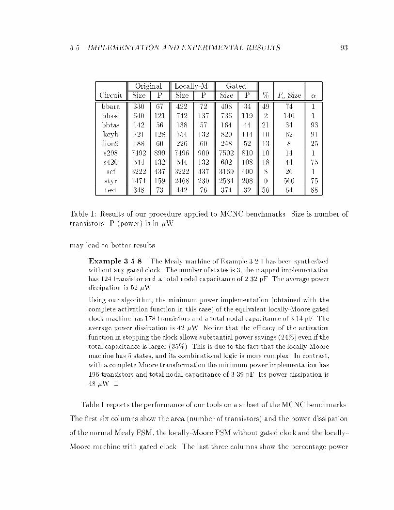
3.5. IMPLEMENTATION AND EXPERIMENTAL RESULTS 93
Original Locally-M. GatedCircuit Size P Size P Size P % Fa Size �
bbara 330 67 422 72 408 34 49 74 1bbsse 640 121 742 137 736 119 2 140 1
bbtas 142 56 138 57 164 44 21 34 .93
keyb 721 128 754 132 820 114 10 62 .91lion9 188 60 226 60 248 52 13 8 .25
s298 7492 899 7496 900 7502 810 10 14 1
s420 544 132 544 132 602 108 18 44 .75scf 3222 437 3222 437 3169 400 8 26 1
styr 1474 159 2468 230 2534 208 0 560 .75test 348 73 442 76 374 32 56 64 .88
Table 1: Results of our procedure applied to MCNC benchmarks. Size is number of
transistors. P (power) is in �W.
may lead to better results.
Example 3.5.8. The Mealy machine of Example 3.2.1 has been synthesizedwithout any gated clock. The number of states is 3, the mapped implementationhas 124 transistor and a total nodal capacitance of 2.32 pF. The average powerdissipation is 52 �W.
Using our algorithm, the minimum power implementation (obtained with the
complete activation function in this case) of the equivalent locally-Moore gated
clock machine has 178 transistors and a total nodal capacitance of 3.14 pF. The
average power dissipation is 42 �W. Notice that the e�cacy of the activation
function in stopping the clock allows substantial power savings (24%) even if the
total capacitance is larger (35%). This is due to the fact that the locally-Moore
machine has 5 states, and its combinational logic is more complex. In contrast,
with a complete Moore transformation the minimum power implementation has
196 transistors and total nodal capacitance of 3.39 pF. Its power dissipation is
48 �W. 2
Table 1 reports the performance of our tools on a subset of the MCNC benchmarks.
The �rst six columns show the area (number of transistors) and the power dissipation
of the normal Mealy FSM, the locally-Moore FSM without gated clock and the locally-
Moore machine with gated clock. The last three columns show the percentage power

94 CHAPTER 3. SYNTHESIS OF GATED-CLOCK FSMS
reduction (computed as 100(Pmealy � Pgated)=Pmealy)), the size (in transistors) of the
activation function and the � factor used in the solution of CPML leading to the best
result. Notice that, if there is no power improvement the improvement is set to 0.
The tool is able to process all benchmarks, but in the table we list examples rep-
resentative of various classes of possible results. The benchmarks bbara and test are
reactive FSMs. The high number and probability of the self-loops allow an impressive
reduction of the total power dissipation, even if the area penalty can be not negligible.
For this class of FSMs our tool gives its best results.
In contrast, for bbsse and styr there is no power reduction or even a power
increase. The bbsse benchmark is representative of a class of machines where the
number and probability of the self-loops is too small for our procedure to obtain
substantial power savings. The styr benchmark has many self-loops, but they all
have low probability. Moreover, the transformation to locally-Moore machine has
a too large area overhead in this case, therefore, even if there are power savings
with respect to the locally-Moore implementation without clock, the smaller Mealy
implementation has the lowest power consumption.
For all other examples in the table the power savings vary between 10% and
30%. For some of these machines (s420 and scf), there is no area overhead for
the locally-Moore transformation. This happens when all states with self-loops are
already Moore states in the original FSM. We included some of the larger examples
in the benchmark suite ( s298 and scf) to show the applicability of our method to
large FSMs.
From the analysis of the results, it is quite clear that several complex trade-o�s
are involved. First, the transformation to locally-Moore machine can sometimes be
very expensive in terms of area overhead. Second, the choice of the best possible
activation function is paramount for good results. In fact, for many examples, the
complete activation function was too large, and reduced activation functions gave

3.5. IMPLEMENTATION AND EXPERIMENTAL RESULTS 95
Circuit PCombGated=P
ClkGated PComb
Loc M=PClkLoc M PComb
Gated =PCombLoc M PClk
Gated=PClkLoc M
bbara 1.2777 2.7006 0.3624 0.7660
bbsse 1.5317 2.5386 0.7601 1.2597bbtas 1.2242 1.8715 0.6861 1.0488
keyb 2.4024 3.2242 0.8185 1.0985
lion9 2.0734 2.2749 0.8937 0.9806s298 17.7560 17.9872 0.9887 1.0016
s420 1.3517 1.5251 0.8126 0.9169
scf 2.8988 2.7368 0.9274 0.8755styr 4.2330 4.3990 0.8969 0.9320
test 1.1751 2.8957 0.3048 0.7512
Table 2: Partition and comparison between power dissipation in clocking logic andFSM logic for locally-Moore and gated-clock FSMs
better results. Notice however that for some examples the e�ciency of the activation
function in stopping the clock was such that the power was sensibly reduced even
with large area overhead.
Having discussed how much power is saved, we address now the problem of where
the power is saved. In our approach the FSM clock is stopped only when the next
state variables and the outputs are not going to change in the upcoming clock cy-
cle. It may be possible to think that power is saved only in the ip- ops and the
clock line. This intuitive observation is deceiving, because power is also saved in the
combinational logic, as it is shown in Table 2. We have compared in the table the
power dissipation of the locally-Moore implementation with and without gated clock.
We compare to the locally-Moore FSM because its STG is isomorphic to those of the
gated-clock FSM. Hence, all modi�cations are due only to the insertion of the acti-
vation function. The comparison with the Mealy machine is less explicative because
the locally-Moore transformation modi�es the STG and consequently the next state
and output function, making impossible to distinguish how the clock-gating circuitry
alone a�ects the power dissipation.

96 CHAPTER 3. SYNTHESIS OF GATED-CLOCK FSMS
In the �rst two columns of the table, for the two implementations, we compare the
ratio of the power dissipated in the combinational logic ( ip- ops outputs, all nodes
in the FSM logic and outputs) and the power dissipated in the clock-related circuitry
(activation function, clock lines, NAND gate, latch, inputs and internal nodes of the
ip- ops). In the last two columns we show the power ratio for the combinational
logic and the power ratio for the clock-related circuitry for the two implementations.
First, notice that the ratio PComb=PClk is almost always smaller for the gated-clock
FSMs. This result is quite intuitive, because PClk in the gated-clock FSM includes
the power dissipation of the activation function. The results of columns 3 and 4 are
somewhat counterintuitive, because they show that there is consistently higher power
saving in the combinational logic than in the clock-related circuitry. This result is due
to three factors. First, the reduced switching activity on the outputs of the ip- ops,
that are generally highly loaded. Second, the absence of propagation to internal nodes
in the FSM logic of input transitions when the FSM is in a self-loops. Third, and
most importantly, the simpli�cation in the FSM's logic that is obtained using the on
set of the activation function as additional controllability don't care set.
We want to point out that our methodology attains consistent power savings not
only when the clock line is heavily loaded and large ip- ops are used, but also for
very small FSMs with optimized ip- ops. It is however important to remark that
the full extent of the possible savings is obtained only if the combinational logic is re-
optimized with the increased don't care set previously described. Moreover, for classes
of FSMs such as synchronous counters, or more generally, FSM without self-loops,
our methodology is ine�ective in reducing power consumption.
In summary, the power savings depend on the fraction of the total operation time
that the FSM spends in idle condition. Don't care optimization is very helpful when
the FSM is small and the idle time is a relatively small fraction of the total, because
it helps in reducing the overhead of the clock-gating circuitry. For large FSMs the

3.6. SUMMARY 97
impact of don't cares is generally less relevant. Even if the power savings are basically
decided by the initial structure of the FSM, it is important to have an automated
synthesis procedure such ours, so as to avoid unnecessary e�ort from designers in
trying to manually design clock-stopping logic.
3.6 Summary
In this chapter we have described a technique for the automatic synthesis of gated
clocks for Mealy and Moore FSMs.
From the practical point of view, we want to emphasize that our method is part of
a complete procedure, starting from FSMs state-table speci�cation to fully mapped
network, and it has been tested with accurate power estimation tools. The quality
of our results depends on the initial structure of the FSM, but we obtain important
power reductions for a large class of �nite-state machines, where the probability of
being in a self-loop (idle) is high. Even if our tool cannot fully replace the knowledge
of the designer in �nding idle conditions at the architectural level, it may enable
design exploration for cases where it is not clear if clock gating may produce sizable
power savings.
From the theoretical point of view, this chapter makes two contributions. First,
we presented a transformation for Mealy FSMs that makes them suitable for gated-
clock implementation, allowing for greater exibility in the choice of clock-stopping
functions with small support and lower complexity. Second, we have proposed a logic
optimization problem, called \constrained probability minimum literals" problem,
and we have described its exact and heuristic solutions. Our solver has large applica-
bility, and can improve the performance of any power management scheme that relies
on optimized combinational logic that stops the clock with maximum e�ciency.
In this chapter we did not address how the presence of the clock-control circuitry

98 CHAPTER 3. SYNTHESIS OF GATED-CLOCK FSMS
a�ects the testability of the gated-clock FSM. This is an important practical issue
that will be addressed in Appendix A. Probably the main limitation in our approach
is its applicability to relatively small sequential system (with a few hundred states)
speci�ed with state tables. In the next chapter we will take a step towards extending
the basic ideas and principles introduced so far to larger sequential circuits described
by synchronous networks.

Chapter 4
Symbolic gated-clock synthesis
4.1 Introduction
In the previous chapter we proposed and e�ective way for obtaining power savings
on a design whose initial speci�cation is given as a state transition graph (STG).
More speci�cally, the strategy adopted to save power is based on the concept of
clock gating. Given the STG of the circuit to be synthesized, conditions under which
the next state and the output signals do not change are identi�ed. In presence of
such conditions, the clock is disabled, since no useful computation is performed by
the circuit, thus avoiding node switching that causes useless power dissipation. We
described techniques for calculating the conditions under which the clock can be
stopped, as well as exact and approximate algorithms for synthesizing the FSM with
embedded clock gating mechanisms.
We now investigate two directions of improvement. First, the algorithms and
data structures described in the previous chapter can e�ectively handle only FSMs
described by state transition tables. Controllers which are automatically synthesized
from high-level speci�cations may have millions of states; explicitly enumerating all
of them in a state transition table, as required by the algorithms described in the
99

100 CHAPTER 4. SYMBOLIC GATED-CLOCK SYNTHESIS
previous chapter, may thus be simply unacceptable. Second, the computation of the
clock gating conditions is performed without considering the controller as a piece of a
more complex system but, rather, as a component running in isolation. This implies
an inevitable loss of information which could have been exploited to achieve a more
e�ective global optimization.
In this chapter we address both the critical issues pointed out above. The problem
of optimizing larger controllers is tackled in two ways. First, by resorting to symbolic
data structures, that is, BDDs and ADDs, to simplify the representation of the clock
gating conditions as well as the calculation of the probability of the activation function
(i.e., the set of clock gating conditions). Second, by employing a new and e�cient
algorithm for the search of the optimal activation function that is able to dynamically
estimate the savings, in terms of power consumption, that di�erent realizations of the
clock gating logic produce on the circuit.
For what concerns the calculation of the activation function, in the previous chap-
ter it was computed by assuming that the FSM is as a self-standing computing el-
ement. We implicitly assumed equiprobable input statistics, because environmental
information were not available. Control-dominated systems are usually interacting
with other controllers and/or data-paths; this may pose some constraints on the sig-
nals that appear at the circuits I/O interfaces. One way of properly modeling the
in uence of the environment on the behavior of a design is through non-equiprobable
primary input statistics. In addition, even when the circuit's primary inputs are to-
tally independent from the other components, there may be cases in which assuming
a 0.5 input transition probability is not realistic (think, for example, to the external
reset signal of a microcontroller). We therefore propose to use non-equiprobable pri-
mary input probability distributions in the computation of the activation function.
Such distributions can be determined from the knowledge of the speci�c functionalities
associated with the various input signals or, alternatively, by performing system-level

4.2. BACKGROUND 101
simulation over a large number of clock periods.
We present experimental results that show the feasibility and the e�ectiveness
of the proposed techniques. Power savings of up to 36% have been obtained on
some of the mid-sized circuits belonging to the Iscas'89 suite [isca89]). Moreover,
experimental data show the impact that an accurate knowledge of the primary input
statistics can have on both the total probability of the activation function and the
power savings obtainable through implementation of the gated clock architecture.
The rest of the chapter is organized as follows. In the next section we brie y review
some background material (refer to Chapter 2 for a more complete treatment). In
Section 4.3 we illustrate how idle conditions can be detected for sequential circuits us-
ing symbolic methods. Section 4.4 describes BDD-based algorithms for the synthesis
the activation function. Section 4.5 and 4.6 discuss the optimization of the activation
function the sequential circuit. Section 4.7 describes an enhancement to the synthesis
of the activation function that allows more idle conditions to be detected. Finally, in
Section 4.8 we report the experimental results.
4.2 Background
We assume the reader to be familiar with the basic concepts of Boolean functions
and with the data structure commonly used for the symbolic manipulation of such
functions, that is, the binary decision diagrams (BDDs). Background material on
this subject has been given in Chapter 2. Recall from Chapter 2 that given a single-
output Boolean function, f(x1; x2; : : : ; xn), the positive and the negative cofactors of
f , with respect to variable xi, are de�ned as: fxi = f(x1; : : : ; xi�1; 1; xi+1; : : : ; xn) and
fx0
i= f(x1; : : : ; xi�1; 0; xi+1; : : : ; xn); the existential and the universal abstraction of
f with respect to xi are de�ned as: 9xif = fxi + fx0
iand 8xif = fxi � fx0
i.

102 CHAPTER 4. SYMBOLIC GATED-CLOCK SYNTHESIS
4.2.1 Sequential Circuit model
We assume the same clocking scheme as introduced in the previous chapter. All ip-
ops are controlled by the same clock, and are all resetable to a given state. Associated
with a sequential circuit is an encoded, Mealy-type, �nite-state machine (FSM) that
describes the behavior of the circuit. An FSM,M , is a 6-tuple (X;Z; S; s0; �; �), where
X is the input alphabet, Z is the output alphabet, S is the �nite set of states of the
machine, s0 is the reset (initial) state, �(x; s) is the next state function (� : X �S !
S), and �(x; s) is the output function (� : X � S ! Z). Boolean functions � and �
have multiple outputs: they implicitly de�ne the state transition graph (STG) of the
given FSM.
Elements x 2 X are encoded by vectors of n Boolean variables, x1; : : : ; xn, called
input variables. Similarly, present states s 2 S are encoded by k Boolean variables,
s1; : : : ; sk, called present-state variables, elements z 2 Z are encoded by vectors of
m Boolean variables, z1; : : : ; zm, called output variables, and next states t 2 S are
encoded by k Boolean variables, t1; : : : ; tk, called next-state variables.
4.2.2 Symbolic Probabilistic Analysis of a FSM
The ADD-based representation of discrete functions has been introduced in Chap-
ter 2 as well as the most important operators for e�cient ADD manipulation: ITE,
APPLY, and ABSTRACT. Remember that the probabilistic analysis of a FSM is
performed studying the Markov chain associated with it. Given the STG of the FSM
representing the circuit and the conditional input probability distribution, we showed
in Chapter 2 that it is possible to compute the vector p whose entries ps are the
steady-state probability of the FSM to be in state s. Unfortunately, the extraction
of the STG from a sequential circuit with many ip- ops is a di�cult task, and the
storage of the STG itself (using traditional data structures such as adiacency lists or

4.3. DETECTING IDLE CONDITIONS 103
Combinational Logic
IN OUT
STATE
GCLK
CLK
&LaF
Combinational Logic
OUT
STATE
CLK
IN
(a) (b)
Figure 24: (a) Single Clock, Flip-Flop Based Sequential Circuit. (b) Gated-Clock
Version.
matrices) is extremely memory demanding.
ADD-based procedures enable the computation of the state probability vector
for very large FSMs (transition graphs with up to 1027 states can be successfully
handled). Note that the the state probability vector is represented by an ADD,
and explicit state enumeration is never required. Complex primary input probability
distributions can be speci�ed and e�ciently represented with ADDs in order to have
more detailed hardware modeling options. We rely on the performance of these
algorithms to overcome some of the limitations which appeared in the implementation
of the optimization methods proposed in the previous chapter.
4.3 Detecting idle conditions
We refer to the FSM implementation with latched inputs introduced in the previous
chapter and reproduced in Figure 24 for the reader's convenience. Given the gate-level
description of the circuit and its probabilistic model, we �rst want to identify the idle
conditions when the clock may be stopped. A gate-level netlist is the implementation
of a sequential circuit that can be represented by a �nite-state machine. In the
following we will refer to the FSM associated with the netlist to clarify some important
points. First, remember that identifying idle conditions is a simple task for circuits

104 CHAPTER 4. SYMBOLIC GATED-CLOCK SYNTHESIS
11/01
11/0001/11
00/11 S3
SS2
1
Figure 25: Fragment of a Mealy FSM. S2 is Mealy-State while S3 is a Moore-State.
implementing Moore-type FSMs. When the present state and the inputs are such
that the next state does not change, the Moore FSM is idle; in symbols: �(x; s) = s
(i.e., the self-loops). We have shown that this property does not hold for Mealy FSMs.
Consider for example the fragment of a Mealy FSM shown in Figure 25. State
S2 has a self-loop, but we cannot stop the clock when we observe the code of S2
and inputs 00 on the state and input lines. The reason is that the self-loop does
not change the next state, but it changes the output if the previous transition was
S1 ! S2. Intuitively, the self-loop on S2 becomes an idle condition only if it is taken
for two consecutive clock cycles. In contrast, the self-loop on S3 is an idle condition,
because every incoming edge of S3 has the same output and knowing that the next
state is S3 provides enough information to infer the output value.
This observation has been formalized in the previous chapter where the states of
a Mealy-type FSM have been divided into two classes. States like S2 where self-loops
are not idle conditions (unless taken twice), are called Mealy-states, while states like
S3 are calledMoore-states. For Mealy-states it is not possible to stop the clock of the
circuit just by observing the state and input lines. Hence, we formulated an algorithm
that operates on the STG of the FSM to transform Mealy-states into Moore-states,
thus allowing the exploitation of more self-loops as idle conditions where the clock
can be stopped.
Our starting point is now completely di�erent: we are not given the STG (or the

4.3. DETECTING IDLE CONDITIONS 105
state table) of the FSM and we want to extract the idle conditions available in the
synchronous network implementing the FSM. It is generally computationally infeasi-
ble to extract the STG representation for large sequential circuits. As a consequence,
the transformation from Mealy-states to Moore-states is not practically applicable
and we must restrict ourselves to the Moore-states of the Mealy FSMs. In other
words, while in the previous chapter we could increase the number of idle conditions
by transforming the STG of the FSM, we will now momentarily assume that only the
self-loops leaving Moore-states of the original FSM can be selected as clock-gating
conditions. This assumption will be relaxed later.
4.3.1 Activation Function
Given an FSM implemented by a synchronous network, we want to �nd the self-loops
of Moore-states. Such self-loops are uniquely identi�ed by the present-state and input
values and represent the set of idle conditions that may be exploited to stop the clock.
For example, for the FSM fragment in Figure 25, the only useful idle condition is the
self-loop on S3 (identi�ed by input value 00 and state value S3).
The complete activation function Fa(x; s) is de�ned by the union of all self-loop
conditions for Moore-states (x and s are respectively the input and state variables).
The set of all self-loops in the FSM includes Fa, because it contains also the self-loops
of Mealy-states.
The identi�cation of the Moore-states can be performed implicitly (i.e., without
extracting the STG) by a procedure that requires a single unrolling of the sequential
circuit, i.e., duplicating the combinational logic to represent two consecutive time
frames, as shown in Figure 26. There are two cascaded logic blocks: the inputs of
the �rst combinational block are x and s, representing respectively primary and state
inputs. The outputs are z and t. The next state outputs t of the �rst block are fed
into the state inputs of the second block. The primary input values in the second

106 CHAPTER 4. SYMBOLIC GATED-CLOCK SYNTHESIS
x
s t
x+
+z z
Combinational logic (1)
Combinational logic (2)
Figure 26: Unrolling of a FSM.
block are represented by x+, while the output of the second block are z+ and the next
state outputs.
With this model, �nding the Moore-states is quite simple. For a Moore state t,
the following property holds: if in the second combinational logic block the state
transition is a self-loop (i.e. �(x+; t) = t), for each state transition s ! t in the
�rst block, the output z = �(x; s) and z+ = �(x+; t) are the same. Intuitively, this
property expresses the requirement that every incoming edge for state t has the same
output value, but we are interested only in states with self-loops, because otherwise
no idle conditions are available. Finding all states for which the condition is true
is equivalent to �nding all Moore-states with self-loops, but no STG extraction is
required. This procedure lends itself to an elegant symbolic formulation that will be
described in the next section.
4.4 Symbolic Synthesis of the Clock Gating Logic
In this section we describe a symbolic algorithm to generate the clock gating circuitry
and we discuss the issues related to the global optimizations that are enabled by
the presence of the new logic into the circuit. The expression giving the activation

4.4. SYMBOLIC SYNTHESIS OF THE CLOCK GATING LOGIC 107
function Fa in symbolic form is the following:
Fa(x+; t) =
kYi=1
��i(x
+; t) � ti�� 8x;s
mYi=1
��i(x; s) � �i(x
+; t)�+ (
kYi=1
(�i(x; s) � ti))0
!
(4.24)
We analyze each term of the seemingly complex Equation 4.24 in greater detail.
� The termQm
i=1(�i(x+; t) � ti) imposes the condition that, in the second frame
of the unrolled circuit, the machine has a self-loop. This is expressed by having
each present-state variable ti identical to the next state function �i(x+; t).
� The termQm
i=1(�i(x; s) � �i(x+; t)) describes the constraint on the output val-
ues. Since we are detecting Moore-states, we require that the output values of
the incoming edge and the self-loop are the same. Notice that the unrolling
implies the use of di�erent variables for the two frames of the unrolled circuit.
� The term (Qm
i=1(�i(x; s) � ti))0 is ORed with the second term to express the fact
that the equality of the outputs in two frames does not need to be enforced for
transitions not in the next state functions of the FSM.
The universal quanti�cation on the inputs x and the state variables s enforces the
condition for all states and input values. Is is important to notice that we do not
use the transition relation of the FSM to compute Fa. This implies that we are
considering all states as reachable, even if this is not generally true. Fortunately, this
assumption does not lead to incorrect implementation.
To justify this claim, consider the following situation. Assume that state s0 is
unreachable, and for input i0, Fa(s0; i0) = 1, in other words, the clock would be
stopped when the state is s0 and the input is i0. However, since s0 is unreachable,
the state lines will never hold that state value, therefore the point s0, i0 in the
controllability don't care set of Fa.

108 CHAPTER 4. SYMBOLIC GATED-CLOCK SYNTHESIS
0/1
0 1
0/0
1/11/0
(a)
0
01
11
10
00
00 01 11 10
x,s
x ,t+
1
1
11
1
1
1
1
0
0
0
0
0
0
0
01
11
10
00
00 01 11 10
x,s
1
1
11
1
1
11
0
0
0
0
0
0
0
0
x ,t+
1 1 00
0
0
0
1
1
1
1
11
0
0
0
01
11
10
00
00 01 11 10
x,s
01
11
10
00
00 01 11 10
x,s
100
1 1 00
0 0 1
1 00
1
1
1
01
11
10
00
00 01 11 10
x,s
x ,t+
1
1
11
1
11
00
0
0
0
0
0
0
1
01
11
10
00
00 01 11 10
x,s
1 1
1
1 1
1 1
1
x ,t+
x ,t+ x ,t+
(b) (c)
(d) (e)
(f) (g)
0
0
0
0
0
0
0
0
Figure 27: Example of symbolic computation of Fa.
The activation function Fa produced by Equation 4.24 is expressed in terms of
the auxiliary variables (x+; t) for convenience, and can be easily re-expressed as a
function of the inputs x and present states s by variable renaming.
Example 4.4.1. Consider the FSM of Figure 27 (a). The next state function�(x+; t) and output function �(x+; t) of the FSM are shown in Figure 27 (b)and (c), respectively. We represent Boolean functions using truth tables, whichare conceptually equivalent to BDDs but more human-readable. The functions�(x; s) and �(x; s) can be obtained by simply rotating the truth tables of �(x+; t)and �(x+; t) by 90 degrees (clockwise), and are not shown.
The truth table of the �rst term in Equation 4.24 (Qm
i=1(�i(x+; t) � ti)) is shown
in Figure 27 (d). The truth table of the second term (Qm
i=1(�i(x; s) � �i(x+; t)))is shown in Figure 27 (e), while the third term (i.e. (
Qm
i=1(�i(x; s) � ti))0) is
shown in Figure 27 (f).
The truth table of the activation function Fa(x+; t) is shown in Figure 27 (g).
The reader can verify the correctness of the result by observing that the Fa is

4.5. OPTIMIZING THE ACTIVATION FUNCTION 109
one in both self-loops of the STG. This is correct, since both states of the FSM
are Moore-states. 2
4.5 Optimizing the Activation Function
Direct application of Equation 4.24 yields, in the general case, functions whose power
dissipation may partially mask o� the potential power savings. Therefore, it is manda-
tory to develop a systematic method to reduce the power consumption of the imple-
mentation of Fa, while keeping as high as possible the probability of its ON-set.
The reader should notice that this is exactly the same problem discussed in Chap-
ter 3 where we formulated an exact procedure for the minimization of a sum-of-
product implementation of Fa. The two main limitations of such procedure were i)
its high computational cost, ii) the fact that we are interested in minimizing power
dissipation of Fa, thus minimizing the number of literals is only a rough approximan-
tion.
In this section we address both limiations: the algorithms presented in this section
are highly e�cient because they operate directly on the BDD representation of Fa,
moreover they explictly target the power minimization of a multi-level implementation
of Fa.
First, we build a pseudo-Boolean function, PFa, which implicitly represents the
probability of the minterms in the ON-set of Fa. Then, we iteratively remove from Fa
some of its ON-set minterms until a given cost criterion breaks the loop. Clearly, both
the minterm removal and the stopping condition must be guided by a combination
of the size improvement in the implementation of Fa and the probability decrease of
the ON-set of Fa. We have devised several heuristics that help in keeping together
these two requirements.

110 CHAPTER 4. SYMBOLIC GATED-CLOCK SYNTHESIS
P
0.25
(b)
T E
0 0.5
T T
EE
P
(a) (c)
T E
T T
EE
1 0
Fa
q
r r
q
r r
Figure 28: The ADD of a two-input probability distributions.
4.5.1 Computing PFa
Let us assume the pseudo-Boolean functions of the primary input probabilities, Pinputs(x)
and of the state occupation probabilities, Pstates(s), to be available (for the details
on how these two functions can be computed implicitly using ADDs the reader may
refer to Chapter 2). The probability PFa can be simply obtained as:
PFa(x; s) = Pinputs(x) � Pstates(s) � Fa(x; s): (4.25)
Obviously, PFa is stored as an ADD, whose paths from the root to the leaves give the
probability of all the minterms in the ON-set of Fa. The total probability of the ON-
set of Fa, (i.e., a real number) can then be computed by applying the ABSTRACT
operator: PROB(Fa) = n+x;sPFa(x; s).
Notice that the ADD representation of the input probabilities Pinputs(x) is com-
plete and accurate. The ADD represents a discrete function that may theoretically
have as many leaves as di�erent values of x. Hence, we can represent exactly any
generic input probability distribution where the inputs have arbitrarily complex cor-
relations.
Example 4.5.2. Consider a circuit with two inputs q and r. Assume that theinputs can assume only the values 00 and 11 and that the occurrences of suchpatterns are equally probable. The probability the �rst input is PROB(q =

4.5. OPTIMIZING THE ACTIVATION FUNCTION 111
1) = :5 and the probability of the second input is PROB(r = 1) = :5. If we nowconsider an input probability distribution where all input patterns 00, 01, 10, 11are equally probable, we still have PROB(q = 1) = :5 and PROB(r = 1) = :5,but the input streams associated with the two distributions are completelydi�erent.
Assume that Fa = qr0 + q0r (we neglect state variables for the sake of simplic-ity). We want to compute PROB(Fa). If we exploit only the information onPROB(p = 1) and PROB(q = 1) we obtain PROB(Fa) = :5(1� :5) + (1 �:5):5 = :5 for both input probability distributions. This is obviously incorrect,since PROB(Fa) = 0 for the �rst distribution, PROB(Fa) = :5 for the second.
The ADD representation allows us to capture the di�erence and to correctly
estimate PROB(Fa) in both cases. The ADDs of Pinputs(x) for the two input
probability distributions are shown in Figure 28 (a) and (b), respectively. The
0/1 ADD (i.e the BDD) of Fa is shown in Figure 28 (c). Multiplying the 0/1
ADD of Fa by Pinputs(x) and applying the ABSTRACT operator lead to the
correct PROB(Fa) value in both cases. 2
4.5.2 Iterative Reduction of Fa
Given the activation function, Fa, and its probability function PFa, the reduction
algorithm iteratively prunes some of the minterms of Fa until an acceptable solution
is found. The pseudo-code of the procedure is shown in Figure 29.
As mentioned earlier, the objective of procedure Reduce Fa is to determine a new
activation function, FBesta , which is contained into the original Fa, has a high global
probability, and is less costly (in terms of both power and area) if compared to Fa.
Three main routines are called inside Reduce Fa:
� Prune Fa eliminates some of the minterms of Fa producing a function whose on
set is strictly contained into that of the origial Fa
� Compute Cost evaluates the power cost of the implementation of the current
Fa. It can be designed to take into account di�erent cost metrics such as area
and timing.

112 CHAPTER 4. SYMBOLIC GATED-CLOCK SYNTHESIS
procedure Reduce Fa(Fa; PFa) f
FBesta = Fa; PBest = PFa ;
FCurrenta = Fa; PCurrent = PFa ;
Best Cost = Compute Cost (FCurrenta );
while (not Stop Test(FBesta ,PBest)) f
FCurrenta = Prune Fa (FCurrent
a );
Curr Cost = Compute Cost (FCurrenta );
if (Curr Cost � Best Cost) f
FBesta = FCurrent
a ;PBest = PCurrent;Best Cost = Curr Cost;
g
g
return (FBesta );
g
Figure 29: The Reduce Fa Algorithm.
� Stop Test is the exit condition. It returns one when it estimated that further
reduction of the on set of Fa cannot improve the circuit's power dissipation.
The algorithm in Figure 29 is a simple greedy procedure that decreases the size
of the activation function until the point of diminishing returns. The quality of
the optimization depends on the implementation of the three routines Prune Fa,
Compute Cost and Stop Test. We discuss them in this order.
4.5.3 Pruning of Fa
We have experimented with two di�erent pruning heuristics. The �rst one is based
on the idea of removing from the ON-set of Fa the minterms whose probability is
smaller than a relative, user-selected threshold, � 2 [0; 1]. Given the probability
function PFa(x; s), we �rst compute the maximum value of its leaves:
Max = nMAXx;s PFa(x; s):

4.5. OPTIMIZING THE ACTIVATION FUNCTION 113
(a) (b)
T
C
ET
0.02
AT E
B BE
C
E ET
T
0.150
AT E
B
C
E ET
T
0.150
Pfa Pfa
Figure 30: Pruning the activation function.
Then we set to 0 all the leaves of the PFa(x; s) ADD whose values are smaller than
�Max, and we set to 1 the remaining leaves. This is accomplished through an ad-hoc
ADD operator called THRESHOLD; we denote as ~PFa the so obtained ADD. Finally,
the current activation function is computed by application of the ITE operator:
FCurrenta = ITE( ~PFa ; Fa; 0):
Preserving a high probability for Fa is essential. However, it is equally important
to keep the area of the clock gating circuitry under control. It is well known that
reducing the number of minterms in the on set of a function does not guarantee that
the size of the corresponding (optimized) circuit decreases. On the other hand, if some
on set minterms are moved to the don't care set instead of the o� set, then the �nal
realization of the circuit can always be better optimized than the original function. To
take this aspect into account, we need to generate the don't care function, DCCurrentFa,
associated with Fa, which can be computed as:
DCCurrentFa= Fa � FCurrent
a : (4.26)
Clearly, DCCurrentFa
can be used to optimize FCurrenta at each iteration of the reduction
process.

114 CHAPTER 4. SYMBOLIC GATED-CLOCK SYNTHESIS
Example 4.5.3. Consider the ADD of PFa shown in Figure 30 (a). Thepaths in the ADD leading to leaves of with non-zero value are minterms ofFa. Thus, the sum of products description of the full activation function isFa = ABC + AB + AB0C, with empty don't care set. We now apply thepruning procedure, with � = :2. The maximum leaf of the ADD has value :15,therefore, the THRESHOLD operator will prune all leaves with value smallerthan :15� = :03.
The ADD of FCurrenta after pruning is shown in Figure 30 (b). Now the sum
of products description of the reduced activation function is FCurrenta = AB +
AB0C. The don't care set is DCCurrentFa
= ABC. 2
In the rare cases where a large fraction of minterms of Fa has the same probability,
we propose a solution based on the concept of BDD subsetting [ravi95]. We retain
only the \dense" subset of minterms with probability p, in the hope that to a small
ADD for the probability function corresponds a compact logic circuit realizing the
reduced Fa. Experimental evidence has proved this choice to be e�ective.
The reduction technique outlined above uses as primary pruning criterion the
probability of the minterms to be added to the don't care set. An alternative heuris-
tic is reminiscent of the strategy presented in [alid94], and it is based on the key
observation that reducing the number of variables in the support of Fa may cause
a reduction in the size of its implementation, since the number of circuit inputs de-
creases accordingly. The second heuristic selects a variable xi to be eliminated from
the support of Fa based on the probability of the universal abstraction qi = 8xiFa(x).
Variables with the highest P (qi) are eliminated, one at a time, until a user-selected
cost requirement (which accounts for both the total probability of the reduced Fa
and the size of its implementation) is met. Also in this case, the reduced activation
function can be further optimized at each iteration of procedure Reduce Fa by using
the don't care information that can be computed using Equation 4.26.
4.5. OPTIMIZING THE ACTIVATION FUNCTION 115
4.5.4 Computing the Cost of Function Fa
The pruning heuristics described in the previous section use, as driving criterion,
the total probability of the reduced activation function as well as the size of its
implementation. However, the ultimate objective of the optimization algorithm is the
reduction of the dissipated power of the overall design. Therefore, the cost function
we employ to decide whether the current solution is acceptable considers power as
primary target. We have considered three di�erent options of increasing accuracy
and computational cost.
1. Curr Cost = POWER(Circuit)(1� PROB(FCurrenta )) + POWER(FCurrent
a ).
This is the simplest cost function; POWER(Circuit) is the average power dis-
sipation of the original circuit, computed through Monte-Carlo or symbolic
simulation. POWER(FCurrenta ), on the other hand, is the average power dissi-
pation of an optimized multi-level implementation of FCurrenta . The �rst term of
the summation represents an estimate of the expected power dissipation of the
circuit when clock gating is present. The second contribution is the additional
power consumed by the activation function. The biggest source of approxima-
tion is in the assumption that the power of the gated-clock circuit (excluding
the activation function) scales linearly with the probability of FCurrenta . The ad-
vantage of this cost function stands in its limited computational requirements,
since POWER(Circuit) is calculated once and for all before starting the Fa re-
duction process. The negative side is, obviously, that the possibly bene�cial
e�ects of simplifying the logic of the overall circuit using FCurrenta as external
don't care set are not accounted for. In contrast, POWER(FCurrenta ) is clearly
recomputed for each new activation function, that is, at each iteration of the
Reduce Fa algorithm.

116 CHAPTER 4. SYMBOLIC GATED-CLOCK SYNTHESIS
2. Curr Cost = POWER(FCurrenta + Circuit).
This is a more accurate cost function. Each FCurrenta is �rst synthesized and
optimized, and then connected to the original circuit as in Figure 24-b. The
power dissipation of the overall network is then estimated. The improved ac-
curacy of this cost function stems from the fact that it does not assume that
the power saved in the FSM is proportional to the probability of the activation
function. On the other hand, the complexity of the computation is increased
because a power estimation of the FSM and the activation function is required
at each iteration.
3. Curr Cost = POWER(OPTIMIZE(FCurrenta + Circuit)).
This is the most accurate cost function. Each FCurrenta is �rst synthesized and
optimized, then it is connected to the original circuit, and the so obtained global
network is optimized using standard techniques which exploit FCurrenta as addi-
tional external don't care set. Notice that the complexity of this cost function is
much higher than the previous two. In this case, the computationally intensive
logic minimization of the FSM logic is performed for each cost evaluation. In
fact, using this cost function is equivalent to generating a set of solutions and
estimating the power savings for each one.
We choose the �rst cost function for the �nal implementation, because its (relative)
low computational cost allowed us to generate and evaluate a much larger number
of reduced activation functions. However, the second activation function may be the
preferred choice for a conservative version of our algorithm. The �rst cost function
may lead to incorrectly predicting power savings for cases where actually there is
power increase. For some circuits the power savings in the FSM logic and ip- ops
may grow less than linearly with the probability of the activation function. If this
is the case, the �rst cost function will bias the algorithm toward excessively complex

4.5. OPTIMIZING THE ACTIVATION FUNCTION 117
(and power consuming) high-probability activation functions.
In contrast, the second cost function is strictly conservative because it assumes
that the clock gating logic is added to the original circuit (i.e. it is fully redundant),
then, power is estimated for the full gated-clock implementation. Compared to the
third cost function, the second one is only more conservative, because it does not
estimate the possible additional power reductions obtainable by optimizing the com-
binational logic of the FSM using Fa as don't care set. As a result, using the second
activation function may lead to convergence on excessively small activation functions
(with almost no power savings), but it will never lead to circuits with increased power
consumption compared to the initial implementation without gated-clock.
The third cost function was not used because of its excessive computational cost,
since the time spent in the optimization of the FSM logic completely swamps the
time spent in all other parts of the optimization procedure. Including this expensive
step in the inner loop of the optimization procedure would intolerably slow town the
search.
4.5.5 The Stopping Criterion
As in any gradient-based re�nement procedure (where the iterations continue as long
as there are improvements, and stop as soon as the cost function starts increasing
again), we reduce the on set of Fa at each iteration and we exit the reduction loop
the �rst time the cost function starts increasing, i.e., Curr Cost > Best Cost . This
choice is based on following observation. The reduction of the activation function is
such that the newly generated Fa is contained into the one generated at the previous
iteration, and therefore once a minimum is hit, it is di�cult to hit another one. This
argument is plausible as long as the circuitry implementing Fa and the original circuit
are kept separated (this is the assumption made by the �rst two cost functions). In
fact, in this case, a smaller activation function improves the power dissipation only

118 CHAPTER 4. SYMBOLIC GATED-CLOCK SYNTHESIS
by reducing the consumption in the clock-gating circuitry. A size reduction of Fa
that increases the power implies that the power not saved in the circuit is larger than
the power saved in the clock-gating circuitry, and using an even smaller activation
function will only make this situation worse.
However, reality is more complex. If we use the most accurate cost function, this
line of reasoning may no longer be correct. This is because a complex Fa with a large
ON set may enable drastic optimizations in the logic of the FSM. Remember that
the ON set of Fa is used as don't care set for the optimization of the FSM logic. It
is clear then that, due to the complexity of the third cost function, �nding a direct
relationship between such function and the optimality of the computed solution is
not an easy task. Moreover, the computational complexity of the third cost function
prevents its use for any large scale example. We therefore chose to trade o� some loss
in optimality of results for the applicability of our method to large circuits.
4.6 Global Circuit Optimization
The result produced by procedure Reduce Fa is a gate-level speci�cation of the acti-
vation function, Fa, which is expected to reduce power dissipation when appropriately
connected to the original sequential design.
After the logic is included in the circuit in the way shown in Figure 24-b, some
global optimization can be performed. Notice that the activation function is func-
tionally redundant. Since we employed redundancy removal procedures targeting
area minimization rather than power minimization, the optimizer may remove the
clock-gating logic in its entirety, thus producing a circuit which is very similar to the
original one. This is most likely to happen when Fa is used as external don't care set
for each primary and state output and redundancy removal methods are used for the
optimization. Clearly, this is something we must avoid.

4.7. COVERING ADDITIONAL SELF-LOOPS 119
The solution we have adopted to overcome this problem consists of adding to
the circuit an extra output pin to make function Fa directly observable. With this
artifact, redundancy removal procedures can be applied to the circuit. This type of
optimization has highly bene�cial e�ects on the gated-clock circuits: not only it may
reduce the power dissipation, it also increases the testability of the system, because it
eliminates the untestable faults in the combinational logic generated by the insertion
of the redundant clock-activation logic [fava96]. Testability issues regarding gated-
clock FSMs are addressed in more detail in Appendix A
4.7 Covering Additional Self-Loops
If a sequential circuit is an implementation of a Mealy FSM with no Moore-states, the
activation function obtained by Equation 4.24 is the null function 0. In this section
we discuss generalizations of the procedure used to �nd the initial Fa that allow the
exploitation of di�erent kinds of idle conditions.
We target self-loops on Mealy states. As discussed above, these self-loops are
not idle conditions because we cannot guarantee that output transitions will not be
required, even if the next state does not change. While in Chapter 3 we solved the
problem by transforming the STG, we now investigate the alternative solution: the
outputs of the sequential circuit are taken as inputs of the activation function as well
as the state and primary inputs.
The gated-clock architecture can be modi�ed as shown in Figure 31. If all outputs
are taken as inputs of the activation function, all self-loops can be exploited to stop
the clock. As an example, consider again Figure 25: if we are allowed to observe the
output values, then a state value of S2, an input value 00, and an output value 11
uniquely identi�es the self-loop in S2. Observing these values we can stop the clock
because: i) the FSM is in a self-loop, ii) the output is not going to change in the next

120 CHAPTER 4. SYMBOLIC GATED-CLOCK SYNTHESIS
Combinational Logic
IN OUT
STATE
GCLK
CLK
&LaF
Figure 31: Modi�ed Gated-Clock Architecture to Take into Account Circuit Outputs.
clock cycle.
The expression of the activation function including output values is very similar
to the one presented in Equation 4.24:
Fa(x+; t; z+) =
kYi=1
(�i(x+; t) � ti) � 8x;s
mYi=1
�i(x+; t) � z+i ) + (
kYi=1
(�i(x; s) � ti))0
!
(4.27)
Notice that the support of Fa has been extended to include the output variables z+.
The termQm
i=1(�i(x+; t) � z+i ) expresses the condition that the observed output value
must be equal to the output that would be computed if we clocked the machine when
traversing a self-loop. If this is true, we do not need to clock the FMS, hence, Fa = 1.
This term is the main di�erence between Equation 4.24 and Equation 4.27: since we
have increased the input support of Fa, we now possess additional information for
stopping the FSM more frequently.
We observed in Chapter 3 that the number of outputs in a sequential circuit is
often very large, thus, the size of the activation logic may increase too much if we
include all outputs in its support. However, it is often the case that we do not need
to use all outputs as inputs of Fa. For example, referring to Figure 25, to exploit the
self-loop on S2 it is su�cient to sample the second output, because the �rst output
does not change on all transition reaching S2. Formula 4.27 can be modi�ed so that

4.7. COVERING ADDITIONAL SELF-LOOPS 121
only a subset of the outputs becomes part of the support of Fa. We have:
Fa(x+; t; z+) =
kYi=1
(�i(x+; t) � ti) �
8x;s
0@ wYi=1
(�i(x+; t) � z+i ) �
mYi=w+1
(�i(x; s) � �i(x+; t))+
(kYi=1
(�i(x; s) � ti))0
!(4.28)
where w is the number of circuit outputs we want to include in the support of the ac-
tivation function. Equation 4.28 can be seen as a compromise between Equation 4.24
and Equation 4.27. The smaller w is, the closest the activation function is to the one
computed by Equation 4.24.
There is clearly a trade-o� between the additional self-loops that can be included
in the activation function by adding one or more outputs to its support and its
size (and power dissipation). We have devised the following heuristic procedure to
perform the selection of an optimal subset of outputs for inclusion in the support of
the activation function.
� For each output, z+i , we �rst compute Fa(x+; t; z+i ) and we determine the value
of its probability. Notice that Fa(x+; t; z+i ) � Fa(x
+; t), therefore PFa(x+;t;z+i )�
PFa(x+;t).
� We build Fa(x+; t; z+) incrementally by adding to the previously computed
activation function the new activation function obtained by inserting one more
output in its support. The outputs are picked in order of decreasing PFa(x+;t;z+i ).
In symbols:
F (0)a = Fa(x
+; t) (4.29)
F (k)a = F (k�1)
a + Fa(x+; t; z+1 ; z
+2 ; :::; z
+k ) (4.30)
The �rst activation function F (0)a is the one computed by Equation 4.24.

122 CHAPTER 4. SYMBOLIC GATED-CLOCK SYNTHESIS
The rationale behind the procedure is that we want to increase the support of Fa
by adding �rst the outputs that contribute more to increasing the total probability
of Fa. After each new F (k)a is generated, we optimize the activation function with the
algorithm described in Section 4.5. The best optimized activation function is chosen.
To reduce the computational burden we stop the generation of new F (k)a as soon
as increasing k by one leads to a new activation function that, after optimization,
performs worse than the last computed one.
4.8 Experimental Results
The power optimization algorithms of this chapter have been implemented within the
SIS [sent92] environment, and their e�ectiveness benchmarked onto some examples
taken from the literature.
The original synchronous circuits have been optimized for area through the SIS
script script.rugged and mapped for speed using the SIS command map -n 1 -AFG.
These mapped circuits have been used as the starting point for our experiments.
The logic for the reduced activation function has been computed through procedure
Reduce Fa and connected to the original circuit as indicated in Figure 24-b. The
functional speci�cation of Fa has then been added as external don't care set for each
circuit output, and the circuit optimized for area through script.rugged.
The library we used for the experiments had NAND and NOR gates with up to
four inputs, and bu�ers and inverters with 3 di�erent size/drive options. Power values
of the initial and �nal circuit implementations were obtained using Irsim [salz89]. All
the experiments were run on a DEC-Station 5000/240 with 64 MB of memory.
Tables 3 and 4 summarize our results obtained on some Iscas'89 synchronous
networks [isca89]. In particular, columns PI , PO and FF of Table 3 show the char-
acteristics of the circuits. Column Gates, Delay and Power tell the number of gates,

4.8. EXPERIMENTAL RESULTS 123
Circuit PI PO FF Before Optimization After Optimization
Gates Delay Power Gates Delay Power
s208.1 10 1 8 90 11.00/10.98 75 95 11.07/ 11.05 49
s298 3 6 14 131 19.26/19.24 89 140 19.90/19.88 72
s386 7 7 6 148 14.94/14.92 63 160 15.97/15.95 58
s400 3 6 21 168 20.81/20.79 90 185 21.14/21.12 63
s420.1 18 1 16 171 16.42/16.40 106 185 17.61/17.59 67
s444 3 6 21 199 20.31/20.29 101 217 22.12/22.10 76
s510 19 7 6 289 25.62/25.60 95 306 27.31/27.29 81
s526 3 6 21 206 18.24/18.22 119 230 19.83/19.81 114
Table 3: Results for Some Iscas'89 Circuits.
the rise and fall delays (in nsec), and the power dissipation (in �W ), before and after
optimization. Columns Variation in Table 4 give the percentage of gate count and
delay increase and power reduction obtained on each example. Finally, column Fa
Time reports the CPU time (in sec) required by procedure Reduce Fa to determine
the simpli�ed activation function.
The cost function used for the the experiments is the �rst one introduced in
Section 4.5.4. We have tested both pruning heuristics for the generation of the optimal
Fa, but the quality of the results did not change sensibly (for the results in the table
we report the best obtained savings).
The size (and the number states, exponentially related to the number of ip-
ops) of the circuits considered in our experiments is such that the application of the
techniques presented in Chapter 3 would be impractical, because of the complexity
of the STG extraction procedure. In contrast, our symbolic algorithms easily deal
with these examples, even with the limited memory available on our machine. To our
knowledge, these are the largest sequential circuits for which gated clocks have been
automatically generated. For some examples the power savings are sizable (25%-
35%), while for others almost no advantage is given by gating the clock. The area

124 CHAPTER 4. SYMBOLIC GATED-CLOCK SYNTHESIS
Circuit Variation Fa TimeGates Delay Power
s208.1 +5% +1% �34% 7.3
s298 +7% +3% �19% 17.8
s386 +8% +7% �8% 69.9
s400 +10% +2% �30% 80.1
s420.1 +8% +7% �36% 150.3
s444 +9% +9% �25% 51.0
s510 +6% +6% �15% 301.3
s526 +11% +9% �4% 120.2
Table 4: Variations in area delay and power, and runtime for some Iscas'89Circuits.
Circuit PI PO States Power SavingsSymbolic Explicit
bbara 4 2 10 45% 49%
bbtas 2 2 6 12% 21%
keyb 7 2 19 26% 11%
lion9 2 1 9 10% 13%
s420 19 2 18 24% 18%
Table 5: Comparison to the Results of the previous chapter on the Mcnc'91 FSMs.
and the delay are kept under control (8% and 5%, increase, on average).
4.8.1 Comparison with the explicit technique
In Table 5 we compare the power savings achieved by the symbolic method to those
obtained in the previous chapter for some of the small, Mcnc'91 FSMs [mcnc91]
(chosen among those for which the explicit algorithm produced the largest savings).
From the results we can conclude that the symbolic approach is not much worse than
the explicit approach, even for FSMs of small size.

4.8. EXPERIMENTAL RESULTS 125
The comparison reveals that in some cases the Locally-Moore transformation de-
scribed in the previous chapter performs better than the output inclusion technique of
Section 4.7, but this is not always true. This fact can be explained by observing that
the Locally-Moore transformation increases the complexity of the FSM logic itself,
while the output inclusion technique has more controllable e�ects, since it modi�es
only the structure of the activation function.
4.8.2 E�ect of input statistics
Since the reactive nature of a controller typically depends on the external environ-
ment, it is likely to happen that idle conditions are exercised when the circuit is
interacting with the components in its neighborhood. We mentioned before that
such interaction may be modeled through non-equiprobable primary input distribu-
tions. Since the computation of the activation function depends on the input prob-
abilities, we expect the size and the probability of Fa to be a�ected by the use of
non-equiprobable input distributions.
We consider, as an example, the minmax3 circuit [coud89], a sequential circuit
that �nds the maximum and the minimum of a stream of numbers. The circuit has
3 inputs: clear, used to reset the maximum and minimum values, enable, whose
function is to prevent the circuit from analyzing some data and the input data port.
We plot the value of PROB(Fa) for varying values of the probability of the enable
(active high) and clear (active low) control inputs (see Figure 32).
For a �xed value of the probability of clear, PROB(Fa) increases as the proba-
bility of enable decreases, and it goes up as the probability of clear increases. This
is reasonable, since a high probability of both enable and clear to be active drives
the circuit into the hold states, corresponding to the traversal of the self-loops of the
STG.
To show how the knowledge of the primary input statistics impacts the synthesis

126 CHAPTER 4. SYMBOLIC GATED-CLOCK SYNTHESIS
0
0.2
0.4
0.6
0.8
1
0 0.25 0.5 0.75 1
PR
OB
(Fa)
p(clear)
p(enable)=0.25p(enable)=0.5
p(enable)=0.75
Figure 32: Case Study: The minmax3 Circuit.
and the re�nement of the activation function, and thus the power savings achievable
with our optimization technique, we present results for the same circuits of Table 3
in which the probability of some of the inputs has been set to values di�erent from
0.5.
Since no information was available for both the circuit functionalities and the
environment in which the controllers are supposed to operate, we have chosen to
modify the statistics of the primary inputs belonging to the support of the activation
function calculated for the equiprobable case. More speci�cally, we have set the input
probabilities so as to emphasize the reactivity of the benchmarks. As expected, power
savings have gone up sensibly.
The results of Table 6 con�rm that power is a strongly pattern-dependent cost
function. It is therefore important to formulate algorithms for power minimization
that can take input statistics into account with the highest possible accuracy. We
showed in Section 4.5 that the ADD-based input statistic characterization is much
more accurate than the simple information provided by input probabilities. As a
consequence, our gated-clock generation algorithm is very exible and e�ective even

4.9. SUMMARY 127
Circuit Equiprobable Inputs Non-Equiprobable InputsPROB(Fa) Power PROB(Fa) Power
Orig. Opt. Savings Orig. Opt. Savings
s208.1 0.314 75 49 34% 0.831 64 17 73%
s298 0.241 89 72 19% 0.902 53 10 81%
s386 0.110 63 58 8% 0.642 52 18 65%
s400 0.249 90 63 30% 0.809 67 15 77%
s420.1 0.311 106 67 36% 0.829 90 21 76%
s444 0.249 101 76 25% 0.811 69 19 72%
s510 0.140 95 81 15% 0.670 81 45 44%
s526 0.244 119 114 4% 0.798 88 43 51%
Table 6: Results for Di�erent Input Probability Distributions.
for complex input statistics with strong correlation between inputs.
4.9 Summary
In this chapter, we presented a fully symbolic approach to the automatic generation
of clock-gating logic for control-oriented sequential circuits. Our methodology starts
from synchronous networks and does not require the extraction of the STG, a very
computationally expensive operation. We leverage the BDD-based representation
of Boolean and pseudo-Boolean functions to extend the applicability of clock-gating
techniques to classes of sequential systems of size unattainable by previous methods
based on explicit algorithms.
The generality of our symbolic formulation enables the application of the synthe-
sis procedure to activation functions with extended support (including some of the
circuit outputs). The compactness and expressive power of ADDs allow us to accu-
rately compute the probability of the activation function, and to formulate algorithms
that control the optimization of the global power dissipation with superior accuracy,

128 CHAPTER 4. SYMBOLIC GATED-CLOCK SYNTHESIS
compared to previous methodologies.
Our power optimization strategy also relies on an integrated synthesis method-
ology that aims at reducing the overhead of the redundant clock-gating logic by
e�ectively exploiting the additional don't care conditions in the combinational logic.
The results are promising, since we obtain power reductions as high as 36%.
Further investigation on this subject will focus on several directions. First, ap-
proximate algorithms for FSM probabilistic analysis need to be developed to further
enhance the scope of applicability of this technique. This is because the real bot-
tleneck of the symbolic approach is the ADD-based calculation of the exact state
occupation probabilities, which becomes infeasible when the circuits contain more
than 50 registers. Constructing and pruning the activation function, on the other
hand, is neither computationally intensive nor too memory demanding. Second, the
problem of estimating the impact of the activation function as additional don't care
set has to be factored into an e�ciently computable cost function.

Chapter 5
FSM decomposition for low power
5.1 Introduction
In the previous chapters we demonstrated that clock gating is an e�ective technique
for minimizing wasted power. Sizable power reduction are obtained for reactive FSMs
that are idle for a large fraction of the operation time. In this chapter we investi-
gate a more aggressive approach: we attempt the minimization of the useful power
dissipation. In other words, we focus on reducing power consumption in sub-systems
that may be idle for a small fraction of the operation time. For such systems, the
clock-gating techniques presented so far are not e�ective.
The fundamental intuition behind the optimization techniques presented in this
chapter is that a sequential circuit may be decomposed into a set of small interacting
blocks. During operation, only one block is active at any given time and controls
the input-output behavior. In the remaining blocks, the clock can be stopped and,
consequently, the total power consumption is reduced. Obviously, a decompostion
approach allows us to save power even for systems that are never idle.
Unfortunately, in many cases the behavior of the system is speci�ed without any
129

130 CHAPTER 5. FSM DECOMPOSITION FOR LOW POWER
consideration for power-e�cient decompositions. Hence, we need to develop proce-
dures for the detection of such decompositions and the synthesis of a hardware archi-
tecture where unused parts of the system can be shut down without compromising
the correctness of the global input-output behavior.
We propose a procedure for the automatic synthesis of a network of interact-
ing FSMs starting from a single state-table speci�cation (or an equivalent format).
We call decomposed FSM the interacting FSM implementation. The straightforward
single-machine implementation is called monolithic FSM. The monolithic �nite-state
machine can be decomposed into smaller sub-machines that communicate through a
set of interface signals. Usually, one single sub-machine is clocked at any given time
and it controls the outputs values while all other sub-machines are idle: they do not
receive the clock signal and dissipate little power. When a sub-machine terminates its
execution, it sends an activation signal to another sub-machine which takes control
of the computation, then it de-activates itself. This transition is characterized by a
single cycle for which both sub-machines are clocked.
There is full cycle-by-cycle equivalence between the input-output behavior of the
decomposed and monolithic implementation. It the FSM is embedded in a larger sys-
tem, the decomposed implementation can replace the monolithic one and the beahvior
of the system remains unchanged.
Given the state transition graph (STG), or equivalently, the state table of the
FSM, our procedure decomposes the STG into a set of smaller STGs. Each com-
ponent is then synthesized using standard FSM synthesis algorithms. The resulting
sequential circuits are then connected and dedicated clock-control circuitry is synthe-
sized, which allows selective clocking of the sub-FSMs. The �nal result is a circuit
that is functionally equivalent to the original speci�cation but has reduced power
dissipation and increased speed compared to an monolithic implementation of the
speci�cation.

5.1. INTRODUCTION 131
The total area of the interacting FSM implementation is larger than that of the
monolithic counterpart. Notice however that the increase in area is accompanied by
more hierarchical structure: the interacting FSMs implementation consists of small
and loosely coupled blocks instead of one large highly coupled block. This charac-
teristic can be very useful during synthesis and the placement and routing phase:
small blocks are more e�ectively synthesized, placed and connected. Consequently
the improved power and performance of our implementation will not be damaged by
excessive wiring even if it has area overhead. Accurate power and timing estimation
shows that the decomposed implementation achieves on average 31% power reduction
and 12% speed improvement at the price of a 48% increase in the number of standard
cells. Since our method trades o� power reduction and speed increase for area usage,
it is well-suited for high-performance VLSI systems where speed and power are the
primary concerns.
It is important to notice that our technique is compatible with sequential power
minimizations such as state assignment [hahe94, tsui94] (see also Chapter 6) and
retiming [mont93], as well as power optimization of the combinational logic [iman96,
baha95, ro 96]. Indeed, after FSM decomposition, the power minimization techniques
can be applied to its components.
5.1.1 Previous work
Finite-state machine decomposition has been extensively studied for several decades.
Its theoretical foundations were laid down by Hartmanis and Stearns [hart66] in
the sixties. Hartmanis and Stearns de�ned several avors of decomposition and for-
mulated numerous decompostion procedures. More recent work [geig91] reports ex-
perimental result on the implementation of the decomposition procedures described
in [hart66].
A di�erent viewpoint on the problem was proposed in recent years by Ashar,

132 CHAPTER 5. FSM DECOMPOSITION FOR LOW POWER
Devadas and Newton [asha91] who presented numerous algorithms for the automatic
decomposition of FSMs speci�ed by an monolithic state transition graph (STG). In
this work, the authors introduced the concept of factorization (an e�cient algorithm
to detect and exploit decomposition opportunities) as well as exact and heuristic
solutions to the problem of two-way FSM decomposition for minimum-area two-level
implementation. The work by Hartmanis and Stearns is based on an algebraic model
of FSMs rooted in lattice theory. By contrast, Ashar et al. rely on Boolean algebra
as the underlying theoretical framework.
More recent work is based on graph theory [royn93, kuo95]. The STG of the FSM
is decomposed using graph partitioning algorithms. Our approach has several points
in common with [royn93]. Most notably, our approach and [royn93] both focus on
a partitioning strategy, where the initial FSM is decomposed in sub-modules that
are never performing useful computation at the same time. However, we target the
minimization of power consumption and we rely on a di�erent assumption on the
hardware implementation (i.e. gated clock versus single clock).
The algorithms mentioned so far target area minimization, or the optimization of
area-related cost functions (i.e. number of input and outputs, connectivity). Although
sizable area reductions can be achieved, the average e�ectiveness of decomposition
techniques for area is not impressive, mainly for two reasons. First, the majority of
real-life FSMs do not have a simple decomposition, and some replication is almost
always required. Second, the computational requirements of the exact decomposition
algorithms are too high on large examples (where the potential savings are substan-
tial), and heuristic solutions fail to �nd good decompositions.
We believe that the potential impact of decomposition techniques for low power
and high performance is much higher. This conjecture is con�rmed in [hasa95], where

5.2. INTERACTING FSM STRUCTURE 133
decomposition techniques have reported very promising delay reductions on multi-
level logic implementation. The experimental results presented in this chapter pro-
vide convinging evidence on the e�ectiveness of the tecompositon approach for power
minimization.
5.2 Interacting FSM structure
Let F = (X;Y; S; s0; �; �) be an monolithic Mealy-type FSM speci�cation, where X
is the input set, Y the output set, S the set of states, s0 2 S the reset state. The
next state function is � : X � S ! S and the output function is � : X � S ! Y .
Assume that a partition � on S is given [hart66]. A partition is de�ned as a
collection of n disjoint subsets of S whose set union is S, i.e �(S) = fP1; P2; :::; Png,
such that Pi \ Pj = ; for i 6= j, andSni=1 Pi = S. We call partition blocks the subsets
Pi.
Given the monolithic F and �(S) we proceed to the formal de�nition of the
decomposed FSM. The decomposed FSM � is a set of n FSMs � = fF1; F2; :::; Fng.
We call sub-machines the FSMs Fi 2 �. A generic sub-machine Fi is de�ned as
Fi = (Xi; Yi; Si; s0;i; �i; i), where:
� s0;i is the reset state of Fi.
� Si, the state set of Fi is Si = Pi [ fs0;ig.
� The input set Xi is Xi = X [ GO�;i. We de�ne GO�;i as follows. For each
transition from a state t 2 Pj to a state s 2 Pi in the monolithic FSM F ,
a new signal got;s is created which is an input for Fi and an output for Fj.
The set GO�;i is the set of all go signals which are inputs for Fi. In symbols:
GO�;i = fgot;s j �(�; t) = s; s 2 Pi; t 2 Pj; Pi 6= Pjg

134 CHAPTER 5. FSM DECOMPOSITION FOR LOW POWER
� The output set Yi is Yi = Y [GOi;�. The set GOi;� is the set of all go signals
which are outputs for Fi: GOi;� = fgot;s j �(�; t) = s; s 2 Pj ; t 2 Pi; Pi 6= Pjg
� The next state function �i(x; goq;t; s) is de�ned as follows:
�i(x; goq;t; s) =
8>>>>>>>><>>>>>>>>:
�(x; s) if s 2 Pi and �(x; s) 2 Pi
s0;i if s 2 Pi and �(x; s) 2 Pj ; Pi 6= Pj
t if s = s0;i and goq;t = 1; q 2 Pj ; t 2 Pi; Pi 6= Pj
s0;i if s = s0;i and 8goq;t 2 GO�;i goq;t = 0
(5.31)
The de�nition means that every transition between states s and t in the mono-
lithic FSM does not change its source and destination if the two states belong
to the same block Pi (this case is shown in Figure 33 (a) and (b)). A transi-
tion from s to t belonging to di�erent partition blocks, respectively Pi and Pj,
becomes: i) a transition from s to the reset state of machine Fi; ii) a transition
from the reset state to t for machine Fj. When a sub-machine Fi is in reset
state, it exits from it only when one of the go signals is set to one.
� The output function �i(x; goq;t; s) takes values on the new output set Yi that
includes the original outputs of the monolithic FSM and the go outputs. We
represent the output value with the notation (x; go).
�i(x; goq;t; s) =
8>>>>><>>>>>:
(�(x; s);0) if s 2 Pi and �(x; s) 2 Pi
(�(x; s); gos;t = 1) if s 2 Pi and �(x; s) = t 2 Pj ; Pi 6= Pj
(0;0) otherwise
(5.32)
We used the shorthand notation (x;0) to indicate that all go outputs or are
held at value 0. Similarly, the notation (0;0) is used to indicate that all original
outputs in set X and all go signals are held at value 0. The notation gos;t = 1
is used to indicate that only one go output has non-zero value, namely gos;t.
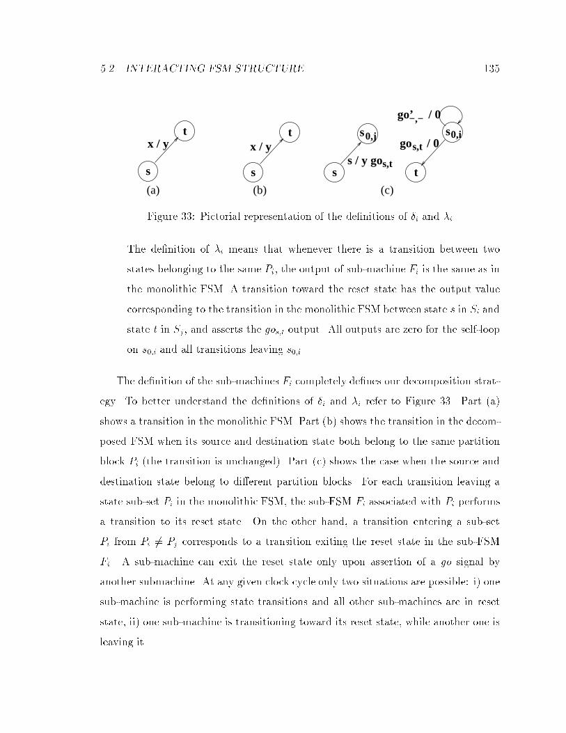
5.2. INTERACTING FSM STRUCTURE 135
s
t
(b)
x / y
s
t
(a)
x / y
(c)
ss / y gos,t
0,js
t
go / 0s,ts0,i
−,−go’ / 0
Figure 33: Pictorial representation of the de�nitions of �i and �i
The de�nition of �i means that whenever there is a transition between two
states belonging to the same Pi, the output of sub-machine Fi is the same as in
the monolithic FSM. A transition toward the reset state has the output value
corresponding to the transition in the monolithic FSM between state s in Si and
state t in Sj, and asserts the gos;t output. All outputs are zero for the self-loop
on s0;i and all transitions leaving s0;i.
The de�nition of the sub-machines Fi completely de�nes our decomposition strat-
egy. To better understand the de�nitions of �i and �i refer to Figure 33. Part (a)
shows a transition in the monolithic FSM. Part (b) shows the transition in the decom-
posed FSM when its source and destination state both belong to the same partition
block Pi (the transition is unchanged). Part (c) shows the case when the source and
destination state belong to di�erent partition blocks. For each transition leaving a
state sub-set Pi in the monolithic FSM, the sub-FSM Fi associated with Pi performs
a transition to its reset state. On the other hand, a transition entering a sub-set
Pi from Pi 6= Pj corresponds to a transition exiting the reset state in the sub-FSM
Fi. A sub-machine can exit the reset state only upon assertion of a go signal by
another submachine. At any given clock cycle only two situations are possible: i) one
sub-machine is performing state transitions and all other sub-machines are in reset
state, ii) one sub-machine is transitioning toward its reset state, while another one is
leaving it.

136 CHAPTER 5. FSM DECOMPOSITION FOR LOW POWER
st0 st1
st3st2
−−/1
−1/11−/0
00/100/1
1−/0−1/0
−−/0
P1
P2 st3st2 −−/0
s02
1−/0−1/0
st0 st1−1/11−/0
−−/1
s01
(a) (b) (c)
st3,st0go’ /0
st1,st2
st1,st2
st1,st2go’ /0
st3,st0
00/1 go
go /0 00/1 go
st3,st0go /0
Figure 34: Decomposition of the monolithic FSM
All inputs and outputs of the monolithic FSM are inputs and outputs of the
sub-machines. The go signals are new, additional inputs and outputs. If an edge
s! t of the original machine has head and tail state included in sub-machine Fi, the
edge is replicated in Fi, with the same input and output �elds. Edges in the global
FSM connecting states which belong to di�erent partitions are associated with edges
representing transitions to and from the reset states of the corresponding sub-FSMs.
These transitions are labeled as follows: i) edges toward reset have the same input
�eld as the original edge, assert an additional output go = 1 and have the same
output �eld as in the original transition edge of the monolithic FSM. ii) Transitions
leaving reset have only one speci�ed input go and all outputs set to zero. The outputs
of a sub-machine blocked in reset state are zero.
Example 5.2.1. Consider the FSM in Figure 34 (a). We assume that the
state partition is �(S) = fP1; P2g = ffst0; st1g; fst2; st3gg. The two sub-
machines created by the decomposition procedure are shown in Figure 34 (b)
and (c). The additional reset states are shaded. P1 originates sub machine
(b) and P2 originates sub machine (c). Notice that the \go" signals are shown
only on the transitions from and to the reset states. A sub-machine asserts a
\go" signal only when transitioning to the reset state, in all other cases the
signal has value zero. Similarly, a submachine is sensitive to input \go" signals
only when it is in reset state. The \go" inputs are not observed for all other
transitions. 2
After describing our decomposition strategy, we now focus on how to reduce the

5.2. INTERACTING FSM STRUCTURE 137
total power dissipation of the interconnection of sub-FSMs.
5.2.1 Clock gating
In the interacting FSM system, most of the machines Fi remain in state s0;i during a
signi�cant number of cycles. If we stop their clock while they stay in reset state, we
would save power (in the clock line, the ip- ops and in the FSM combinational logic)
because only a part of the system is active and has signi�cant switching activity. To
be able to stop the clock, we need to observe the following conditions.
� The condition under which Fi is idle. It is true when Fi reaches the state
s0;i. We use the Boolean function is in reseti that is 1 if Fi is in state s0;i, 0
otherwise.
� The condition under which we need to resume clocking, even if the sub-FSM is
in reset state. This happens when the sub-FSM machine receives a go signal
and must perform a transition from s0i to any other state.
We can derive Fai, the activation function (in negative logic). The clock to Fi is
halted when Fai = 1. Namely:
Fai = is in reseti ^ (_
q2Fi; p2Fj 6=Fi
gop;q) (5.33)
The �rst term is in reseti(s) stops the clock when the machine reaches s0;i. The
second term ensures that clock is not halted when one of the gop;q is asserted and
the sub-FSM must exit the reset state. This activation function allows the newly
activated sub-FSM to have its �rst active cycle during the last cycle of the previously
active FSM. The two sub-FSMs make a transition in the same clock cycle: one is
transitioning to its idle state, and the other from its idle state. The local clocks of

138 CHAPTER 5. FSM DECOMPOSITION FOR LOW POWER
Fi and Fj are both active. We call transitions of control the cycles when a sub-FSMs
shuts down and another activates.
Each local clock of the FSMs Fi is controlled by a clock-gating circuit. The circuit
implements the activation function Fai. We could use Fai directly as enable signal
on the ip- ops, but this scheme would let the clock lines active and consume power,
therefore we choose an aggressive implementation: the clock itself is stopped when a
submachine is inactive. The power savings on the clock are sizable because the clock
line is heavily loaded and switches with high frequency. We use a low-level sensitive
latch for Fai, in order to avoid spurious transitions on the clock line that would result
in incorrect behavior. Refer to Chapter 3 for a detailed description of the clock-gating
circuitry.
The clocking strategy discussed so far has two important functions: reducing
power dissipation and keeping the sub-FSM in lock-step. We now address the issue of
ensuring cycle-by-cycle equivalence between the monolithic FSM and the decomposed
implementation. The outputs of the gated-clock sub-machines are connected to n-
way OR gates, one for each primary output. The output equivalence between the
decomposed machine and the speci�cation is guaranteed by the fact that, at any
given clock cycle, only the active sub-machine is controlling the output value, and
all inactive sub-FSMs have their output forced to zero. During the transitions of
control, when a machine stops and another resumes execution, the value of the output
is controlled by the machine terminating execution.
Example 5.2.2. The gated-clock implementation of the interacting FSMs of
Figure 34 is shown in Figure 35. Notice how the external output is obtained by
OR-ing the outputs of the sub-FSMs. Figure 35 also shows the clock waveforms,
the \in reset" signals and the \go" signals. Notice that there is a clock cycle
for which both local clocks are enabled. The waveforms show how sub-FSM 1
is deactivated and sub-FSM 2 activates thanks to the assertion of the gost1;st2signal. 2

5.3. PARTITIONING 139
RESETres
L
L
CLK
Fa1
Fa2
in
in
out
out
res
in_res1
in_res2
INPUT
clk1
clk1
clk2
CLK
go
in_res1
in_res2
out
F2
F1
gost1,st 2
gost3,st0
clk2
st1, st2
Figure 35: Gated-clock implementation of the interacting FSMs
The startup of the decomposed FSM is obtained by disabling Fa for all sub-FSMs
when a synchronous RESET is asserted (this can be done by inserting a AND gate
controlled by RESET on the output of Fa). When the RESET signal is high, all
sub-machines receive the clock signal. Notice that only the sub-FSM containing the
original reset state of the monolithic FSM is actually set to the corresponding state
code. All other machines are put in reset state s0;i and they stop and wait for an
external go signal.
5.3 Partitioning
The power savings in the interacting FSM implementation strongly depends on the
quality of the partition �(S). A good partition is characterized by loose interaction
between sub-FSMs and small communication overhead. We analyze these require-
ments in detail.
The ideal mode of operation for the interactive FSM circuit is one of minimum
transition of control between di�erent sub-FSMs. When a sub-FSMs disables itself
and another one takes control, both machines are clocked for one cycle, the go signals

140 CHAPTER 5. FSM DECOMPOSITION FOR LOW POWER
involved in the control transfer change value, and the clock control circuitry switches
as well. As a result, transitions of control are power consuming and should be avoided
as much as possible.
Minimizing the number of go signals is another important objective. The gener-
ation of such signals requires additional hardware, that increases power dissipation.
Moreover, the go signals increase the coupling between sub-machines, complicating
the placement and routing of the circuit. On the other hand, if we reduce the num-
ber of go signals to zero, i.e. we do not decompose the FSM, no power savings are
achieved.
In summary, we should look for a partition �(S) which maximizes the locality of
the computation and minimizes the hardware overhead for communications between
sub-FSMs. We formally describe this problem in the next subsection.
5.3.1 Partitioning as integer programming
In the following discussion we assume that the probability of occupancy of every state
in the original FSM has been computed. This task can be performed by simulating
the behavioral description of the FSM or by an analysis based on a Markov chain
model, as seen in Chapter 2.
The problem of �nding an optimal partition �(S) can be formalized as an Integer
Programming (IP) problem [nehm88]:
Given:
ai, the probability to be in state i,
bij, the probability to transition from state i to j,
nmax, the maximum number of blocks in the state partition.
A set of binary decision variables fxip, i = 1; 2; :::; jSj, p, p = 1; 2; :::; nmaxg such that
xip = 1 if state i in partition block p and 0 otherwise.

5.3. PARTITIONING 141
Minimize:nmaxXp=1
Kp � Prob(Fp) (5.34)
With constraints:nmaxXp=1
xip = 1;8i (5.35)
i.e. every state has to be assigned to exactly 1 partition.
The formulation of the cost function requires further discussion. The cost of the
interacting FSM implementation can be expressed as the summation over all sub-
FSMs of the cost of each sub-machine (Kp) weighted by its probability to be active
(P (Fp)). The cost of a sub-machine is expressed by a linear combination of the
number of states of the machine and the number of possible transitions from and
to the sub-machine (meaning extra I/O). This is can be expressed by the following
equation:
Kp =
1 +
Xi
xip
!+ �
0@Xp1 6=p
Xi
Xj
dbijexip1xjp +Xp2 6=p
Xi
Xj
dbijexipxjp2
1A (5.36)
The �rst part of the formula is simply the number of states in partition block
p. The second part of the formula accounts for the transitions connecting states in
p with states in other partition blocks. The term dbijexip1xjp is 1 if the transition
probability from state i to state j is bij > 0, with i in partition block p1 and j in
p. It is zero otherwise. By summing over all edges (a sum over i and j) and all
partition blocks p1 di�erent from the one under consideration, we obtain the total
number of transitions into p. Similarly, the term dbijexipxjp2 holds value 1 only for
transitions with non-null probability from a state in partition block p to a state in
another partition block.

142 CHAPTER 5. FSM DECOMPOSITION FOR LOW POWER
The rationale behind the cost function is that we look for a decomposed im-
plementation with minimum interface cost. The �rst part of the formula penalizes
implementation with excessively coarse granularity, while the second part penalizes
implementations where the interface overhead is high. The coe�cient � expresses
the relative weight that should be given to minimizing the additional gates and wires
needed to implement the interface between sub-FSMs (i.e. the go signals and the
logic generating them) with respect to the number of states of each sub-FSM (i.e. the
granularity of the decomposition).
The probability that a particular machine Fp is powered, Prob(Fp) is equal to
the total state occupancy probability for states in Fp plus the total probability of
transition to Fp. From other partition blocks. In symbols:
Prob(Fp) =Xi
aixip +Xp1 6=p
Xi
Xj
bijxip1xjp: (5.37)
Notice that it is important to consider the probability of the incoming edges
for each partition because they mark transitions of controls. During transitions of
controls two sub-machines are powered on at the same time. Therefore, the summation
of Prob(Fp) over all sub-machines Fp is larger than one, accounting for the cycles
when two sub-machines are enabled. The formalism used for the IP formulation will
be clari�ed through an example.
Example 5.3.3. Consider the FSM speci�ed by the STG in Figure 34 (a),reproduced in Figure 36. We assume equiprobable and independent inputs forthe sake of simplicity. From the input probability distribution and the STG,the state probabilities are computed: [1=4; 1=4; 1=4; 1=4]T . The transition prob-abilities are computed from state probabilities and input probabilities. Theyare collected in the transition probability matrix:
26664
0 1
40 0
3
160 1
160
0 0 0 1
41
160 3
160
37775

5.3. PARTITIONING 143
st0 st1
st3st2
−−/1
−1/11−/0
00/100/1
1−/0−1/0
−−/0
Figure 36: STG of the example FSM
We assume a 2-way partition of the states, where st0 and st1 are assigned toblock 0 and st2 and st3 to block 1 . The partition is expressed by the matrixof xip: 2
666410100101
37775
Notice that this matrix is constrained by the fact that every row sums up to1, since every state is assigned to exactly one partition. We calculate the costfor partition block P1. The �rst term is 1 +
Pi xip = 3, which counts the 2
states of block P1, st0, st1 and the reset state the sub-machine goes intowhen it is powered down. The second term in the cost function consists oftwo contributions: i) incoming edges, ii) outgoing edges. There is only oneincoming edge, namely for i = 3; j = 0; p1 = 1, and one outgoing edge, fori = 1; j = 2; p2 = 1. The cost for P1 is therefore 3 + �(1 + 1).
The probability to be in P1 is 1=2. We know from the cost calculation thatthere is 1 possible transition into this partition, for i = 3; j = 0; p1 = 1.The probability of this transition is b30 = 1
16. Note that the probability of
transitioning out of the partition equals the probability of transitioning into it.We only have to count one of both. Hence, the total probability is for P1 to bepowered is 9
16.
The total cost function for this example is given by the scalar product of the
matrix of costs for each partition and the matrix of the probabilities for each
partition to be powered. Considering the symmetry of the example and choos-
ing � = 1, we get 5 9
16+ 5 9
16= 45
8. 2

144 CHAPTER 5. FSM DECOMPOSITION FOR LOW POWER
Several techniques have been proposed solve the IP problem exactly and heuristi-
cally [nehm88]. The exact solution of IP requires algorithms with above-polynomial
worst-case complexity since IP is NP -complete [nehm88]).
5.3.2 Partitioning algorithm
In our case, exact minimization is unnecessarily computationally expensive because
the cost function is only an approximate measure of the quality of a partition �(S),
which is dependent on the power dissipation of the decomposed implementation. We
implemented a heuristic solution based on a genetic algorithm [gold89] (GA) which
still leverages the IP formulation of the problem. Some properties of the problem
made it well suited for this approach. First, the solution space is easily representable
as a set of bit-strings: a chromosome is encoded as a set of jSj blocks of dlog2nmaxe
bits. Each block is associated with a state and represents the number identifying the
partition block to which the state belongs. The length of the chromosome in bytes is
jSj � dlog2nmaxe=8. This is a very compact encoding and if nmax is chosen as a power
of two, every chromosome represents a valid solution.
Second, the crossover operator is meaningful. If in a given generation the genetic
search �nds a set of states which are good candidates for clustering, thanks to the
crossover operator, the substring representing the set of states will be replicated with
high probability in successive generations.
Third, and more importantly, the cost function can be e�ciently evaluated, and
its computation is O(jEj) where jEj is the number of edges in the STG of the original
machine. The compact encoding (with no invalid solutions) and the inexpensive
computation of the cost function allow us to take very large populations (in the order
of 106 individuals).
To e�ciently evaluate the cost function, the state probability vector and the transi-
tion probability matrix of the monolithic FSM are stored once for all at the beginning

5.3. PARTITIONING 145
foreach (state i) f /* Compute partition probabilities */
Cost[partition(i)] ++;
probability[partition(i)] += StateProbability(i);
g
foreach (edge i ! j) f /* Compute cost of transitions of control */
if (partition(i) 6= partition(j)) f
probability[partition(i)] += TransitionProb(i!j)
Cost[partition(i)] += �
Cost[partition(j)] += �
g
g
TotalCost = 0;
foreach (partition p) f /* Compute total cost */
Cost[p] ++;
TotalCost += Cost[p] * probability[p]
g
Figure 37: Algorithm for the computation of the cost function
of each GA run. Other inputs parameters are the relative cost of the I/O overhead
(parameter � in Equation 5.36) and the maximum number of partitions to consider
nmax. The simpli�ed pseudo-code for the evaluation of the cost function in the genetic
algorithm is shown in Figure 37.
There are three loops in the algorithm. The �rst iterates over all the states to
compute the �rst part of the cost function (P
i xip) and the cumulative probability of
the states in each partition. The second loop computes the second part of the cost
function (i.e. the cost of the interface signals) and the probability of the transitions
of control. Finally, the third loop iterates on the partitions and computes the �nal
value of the cost function (i.e. the weighted sum of Equation 5.36). The worst case
complexity is O(jEj) because, for non-sparse STGs, the number of edges is of the
order of jSj2. The second loop usually dominates the execution time.
It is important to notice that our optimization strategy not only tries to �nd an
optimal partition, but also automatically searches for an optimal number of blocks in
the partition. In particular, if the circuit is not decomposable in a favorable way, the
GA run will produce a degenerate partition consisting of a single block containing

146 CHAPTER 5. FSM DECOMPOSITION FOR LOW POWER
all states of the original FSM. The only constraint on the partition is the nmax, the
maximum number of allowed blocks.
Concluding this section, we point out that our optimization strategy is based on
a cost function which is not directly proportional to the actual power dissipation.
However, the experimental results con�rm that our cost measure is very informative
in the relative sense (i.e. it can be used to compare the power dissipation of two alter-
native decomposed implementations). If one partition has much better locality and
lower interface cost than another one, the power dissipation of the �rst will be usually
much smaller than the second one. This is because our gated clock implementation
guarantees that only a small part of the system is active at any given cycle, therefore
a system with few transitions of control and few go signals dissipates less power than
a system with poor locality and high interface overhead.
Notice also that our technique can be biased by increasing the relative cost of
the interface overhead in the cost function. Changing the value of coe�cient � the
user can control the likelihood of the generation of a decomposed implementation.
Moreover, by controlling nmax the user can set a lower limit to the granularity of the
partition.
5.4 Re�ned model for partitioning
In the previous sections we have assumed that every transition between states of
two di�erent partition blocks corresponds to an additional interface signal in the
interacting FSM implementation. This is a safe but conservative assumption. In
many cases the number of interface go signals can be highly reduced.
The reduction in the number of go signals is based on the following observation.
When the control is transferred from one sub-FSM to another, the only information
that the newly activated machine needs is the destination state to which it has to

5.4. REFINED MODEL FOR PARTITIONING 147
1−/100/0
s1 s3
s4
−−/000/1
(a)
s2
01/11−/0
01/0
00/1
1−/101/1
s1 s3
s4
−−/0
s2
00/1
1−/1
01/0
11/1
01/1
(b)
1−/1
00/1
0−/0
10/0
s1 s3
s4
−−/0
s2
00/1
1−/101/1
1−/100/0
00/101/1
1−/0
01/0
(c)
Figure 38: Decomposition of the monolithic FSM
transition. Assume that there are two incoming edges from states in block Pi to
states in block Pj of the state partition. If the two edges are directed to the same
state in Pj , there is no need to have two di�erent go signals, because sub-machine
Fj should transition to the same state when it is activated by submachine Fi. The
output values during the transfer of control are not a problem, because they are set
by Fi, which can distinguish between the two transitions, since they are originating
from two di�erent states.
Even if the two edges go to di�erent states in Pj , we might be able to use the
input signals that caused the transitions to discern between the destination states. If
the input value labeling the transitions are di�erent, we can use them in sub-machine
Fj to direct the transition from its reset state towards the right destination. The only
case when we need to implement more than one go signal between two sub-FSMs is
if there are transitions to multiple states in Fj which are not distinguishable by their
input �elds.
Example 5.4.4. Consider the STGs of three monolithic machines shown in
Figure 38. In each FSM, states s1 and s2 belong to the same partition block,
states s3 and s4 belong to another. The edges drawn with thick dashed lines
represent transitions of control in the decomposed implementation from the �rst
to the second sub-machine, while the edges drawn with thin dashed lines are
transitions of control from the second to the �rst sub-machine. We focus on the
transitions of control from the �rst to the second sub-machine. Figure 38 (a)
shows a case where two edges between partition blocks do not require two \go"

148 CHAPTER 5. FSM DECOMPOSITION FOR LOW POWER
if( list of edges from partition(i) to partition(j) == NULL ||
( list of edges from partition(i) to partition(j)
contains an edge going to a different state &&
being triggered by the same input &&
doesn't contain an edge to this state for which a signal was added)) f
Cost[partition(i)] += �
Cost[partition(j)] += �
g
add (i,j) to list of edges from partition(i) to partition(j);
Figure 39: Improved computation of the cost function
signals in the interacting FSM implementation, because they are both directed
towards the same state. Figure 38 (b) shows another case that requires only
one \go" signal, since the input �eld in the two edges allows to distinguish
the destination state. The situation shown in Figure 38 (c) requires two \go"
signals. The input on the edges cannot be used to distinguish the destination
state when, in the decomposed implementation, the sub-machine containing s3
and s4 is activated by the sub-machine containing s1 and s2. 2
Reducing the number of interface signals gives us muchmore freedom in the choice
of the partition. Moreover, many controllers have STG that cannot be partitioned
without cutting numerous edges. For these controllers the basic technique proposed
in the previous section would not �nd any acceptable partition but the trivial one
(i.e. the unpartitioned state set), while the improved partitioning technique leads to
e�ective decompositions.
Since our improved decomposition technique can greatly reduce the number of go
signals required in the interface of the sub-FSMs, the cost function used during the GA
to evaluate the quality of a partition is modi�ed accordingly. In the cost function,
the number of outgoing and incoming edges is replaced by the actual number of
output and input signals to be added to the machine. This is calculated using the
pseudo-code of Figure 39, which replaces lines 8 and 9 in the original algorithm.

5.5. EXPERIMENTAL RESULTS 149
5.5 Experimental results
We speci�cally designed the FSM decomposition tool for seamless embedding into
pre-existing synthesis-based design ows. The tool consists of two programs: the
partitioner and the netlister. The partitioner reads in the STG of the monolithic
FSM and �nds an optimal partition �(S). The frame for the genetic algorithm
implemented in the partitioner is provided by the Genesis package [gref90]. The
netlister reads in the partition �(S), the STG of the speci�cation and produces the
decomposed FSM. One important task of the netlister is the reduction of the number
of go signal, which is performed following the approach outlined in Section 5.4.
The input of our tool is a simple state table description (in Berkeley kiss format
or in the similar Synopsys state table format) and a �le containing the state and
input signal probabilities. The output is a set of state tables, one for each partition
of the decomposition and a synthesizable Verilog description of the clocking circuitry,
containing empty modules corresponding to the sub-machines. Thanks to this simple
interface, the user can just read the Verilog code and the state tables in the logic syn-
thesis tool of choice and proceed to the logic-level optimization of the full hierarchical
design.
We also implemented a program for the computation of the state probabilities
given the input probability distribution based on Markov analysis (see Chapter 2).
This is a simple utility that can be used when the state probabilities are not known.
Alternatively, the user can just simulate the behavioral description of the FSM and
collect information on the state occupancy probability. We do not rely on any limiting
assumption on state or input probability distribution, our decomposition algorithm
simply assume that this data is externally provided.
The time spent in decomposition strongly depends on the e�ort that the user want
to dedicate to the search of an optimal solution. This is controlled by a parameter �le

150 CHAPTER 5. FSM DECOMPOSITION FOR LOW POWER
that is speci�ed once for all by the user and is used to set-up the GA run and control
the parameters in the cost function. The �le contains: i) parameters for the GA
run (population size, number of cost function evaluations, probability of cross-over
and mutation, and other secondary parameters); ii) the values of nmax and � for the
control of the cost function. In our experiments we wanted to explore the maximum
optimization achievable, therefore we speci�ed large population sizes (from 105 to
106) and large numbers of cost function evaluations (from 106 to 5 � 107). Our GA
runs were scheduled for overnight runs on SGI Indy machines with 64Mb of memory.
The parameters for the control of the cost function have been the subject of
careful study. With our technology library, � � 1 gave the best results. If pre-layout
estimates of the interface cost are considered too optimistic, the value of � can be set
to a constant larger than one. Also, � is technology dependent and could change with
the technology library used for mapping. The maximum number of partition blocks
nmax was always set nmax = 8, since initial exploratory analysis with larger nmax
showed that solutions with more than 8 sub-machines were never included among the
best individuals of the GA runs.
Table 7 shows the results on a number of benchmarks. The �rst three examples
are controllers of data-path small full-custom chips implemented in a class project.
The remaining FSMs are standard MCNC benchmarks [mcnc91], with the exception
of the last one which is a modi�ed version of MCNC benchmark s298 (we reduced
the number of states because the commercial tool we used for FSM synthesis could
not optimize the monolithic implementation with the memory resources available on
our machines).
The decomposed and monolithic implementation were both optimized with Syn-
opsys Design Compiler running on a Sun SPARC10 workstation, using the same
optimization script targeting minimum delay. The circuit power was estimated by

5.5. EXPERIMENTAL RESULTS 151
Name Original Partitioned# of # of # of std power crit. # of std power crit.states partitions cells path cells path
test1 24 4 67 804 3.81 118 679 3.01(+76%) ({16%) ({21%)
test2 18 3 58 930 2.83 89 642 2.98(+53%) ({31%) ({5%)
test6 80 4 252 2115 7.09 336 1209 5.92(+33%) ({43%) ({17%)
bbsse 13 4 112 1146 4.21 145 847 3.60(+29%) ({26%) ({14%)
dk512 14 2 61 1138 3.29 88 853 2.79(+44%) ({25%) ({15%)
keyb 18 3 157 1688 4.15 262 1387 4.69(+67%) ({18%) (+13%)
planet 48 4 360 4967 6.76 503 3241 5.85(+40%) ({35%) ({13%)
s1488 48 4 433 2743 6.68 642 1717 5.82(+48%) ({37%) ({13%)
s820 25 3 191 1717 5.01 238 1171 3.83(+25%) ({32%) ({24%)
s832 25 3 211 1889 4.61 274 1244 3.72(+30%) ({34%) ({19%)
sand 32 4 429 3395 7.86 471 2554 6.78(+10%) ({25%) ({14%)
scf 112 8 672 3719 7.07 988 2280 5.36(+47%) ({39%) ({24%)
test13 166 8 681 7006 7.38 1610 4124 7.57(+137%) ({41%) (+3%)
Table 7: Power, area and speed of the decomposed implementation versus the mono-
lithic one
152 CHAPTER 5. FSM DECOMPOSITION FOR LOW POWER
PPP[bogl96], an accurate full-delay gate-level power estimator. The critical path tim-
ing was estimated after technology optimization by the static timing analysis tool
within Design Compiler. Our technology library is a subset of the Berkeley Low-
Power CMOS library [burd94]. Interestingly, for all larger examples in the table, the
run time of the synthesis tool was much decreased for the decomposed implementa-
tion.
The di�erences in area, power and speed between the partitioned machine and the
original unpartitioned design is given in Table 7 between parentheses in the last three
columns. The average power reduction is 31%. There is also an increase in speed
of 12%. The number of standard cells increases on average by 48%. The results
listed are only for machines that actually are successfully partitioned. Some designs
do not have an e�ective partitioning, and they are left monolithic by our tool. For
example, in the MCNC benchmark suite, the FSMs bbara, bbtas, dk16 and donfile
are not decomposed. Notice that, with the values of Pmax and � we chose, the tool
never produced partitioned machines with power consumption larger than the original
one. This indicates that i) our technique is conservative ii) more aggressive settings
(for example, � < 1) could lead to the decomposition of more machines, but the
uncertainty on the quality of the results would increase.
Notice also that the increase in area is marked on all the examples. The main
reason for this phenomenon is the overhead due to additional ip- ops. We speci�ed
minimum-length state encoding in all our experiments. This encoding style implies
that the number of ip- ops in the monolithic machine increases only logarithmically
with the number of states. When the machine is decomposed, the number of states
in each sub-machine is decreased by a factor of two if the partition is balanced. In
this case each sub-machine has just one ip- op less than the original machine and
the total number of ip- ops is almost doubled. If the partition is unbalanced, the
number of ip- op is generally increased by the ip- ops required in the smaller

5.6. SUMMARY 153
machine. Obviously the sequential overhead is larger for N -way partitions, with
N > 2. We could have performed our tests specifying one-hot encoding. In this case,
the sequential overhead would have been null. However, we feel that the comparison
with minimum-length encoding is fairer towards the monolithic implementation.
It can be observed that the increase in area may translate after layout in increase
in power and delay. However our implementations are more modular, because they
consist of small and loosely connected blocks. This characteristic may actually im-
prove the quality of the layout. Moreover, the power savings are quite large and
unlikely be completely swamped during layout.
5.6 Summary
We have described an algorithm for �nite-state machine decomposition for low power
consumption. We leverage clock-gating techniques to produce an interacting FSM
implementation in which only one or two sub-machines are clocked at any clock
cycle, while the others are inactive and dissipate small power. Our tool integrates
easily in synthesis-based design methodologies and can be seen as a pre-processing
step on the state table speci�cation of the original FSM. Standard synthesis tools (or
the techniques illustrated in previous chapters) can then be used for optimizing the
sub-FSMs and additional power reductions can be obtained.
Our partitioning algorithm takes into account the overhead imposed by the in-
terface signals required for the interaction of the sub-machines and automatically
chooses not only how to partition the state set of the original speci�cation, but also
how many partition blocks will be generated. The algorithm is based on conservative
assumptions and avoids the generation of decomposed FSMs if the expected power
savings are not high. An important byproduct of our technique is the increase in
speed of the interacting FSM.

154 CHAPTER 5. FSM DECOMPOSITION FOR LOW POWER
The search for an optimal decomposition is based on a Genetic Algorithm and
it is therefore heuristic in nature. However, the compact encoding scheme and the
e�cient computation of the cost function allow us to search e�ectively the solution
space by selecting large population sizes. The results achieved by our algorithm are
very promising: on average, 31% power reduction, 12% speed increase at the price of
a 48% area increase are observed for FSMs that are decomposed.
Several extensions of the decomposition approach are possible. First, determin-
istic graph-based algorithms can be used for improving the quality of the partition,
since the genetic algorithm is a randomized general-purpose technique that does not
exploit information on the particular structure of the optimization problem. Tailored
heuristics may outperform the GA both in speed and quality of results. Moreover, it
is possible to extend the decomposition technique to deal with large sequential sys-
tems for which the state table is not available (or too large to be handled). This can
be accomplished by leveraging implicit state-space decomposition algorithms such as
those presented in [cho94] and the ADD-based approach introduced in Chapter 4.

Chapter 6
State assignment for low power
6.1 Introduction
As seen in previous chapters, the behavioral speci�cation of a �nite-state machine
is typically in the form of a state transition graph, where each state is represented
symbolically. In Chapter 2 we de�ned state assignment as the synthesis step where
binary codes are assigned to the symbolic states. The designer (or the synthesis tools)
is free to decide the length of the code words (i.e. the number of state variables) and
the encoding of each state. Such degrees of freedom can be exploited to obtain an
optimized implementation of the FSM.
Earlier approaches to state assignment have targeted area and performance both
for two-level and multi-level logic implementation ([dmc86] [esch92], [asha91] and
[dmc94] are good surveys of previous work). In this chapter we investigate state
assignment algorithms targeting low power dissipation.
Compared to the approaches described in previous chapters, state assignment does
not require any manipulation of clock-related circuitry. However, it has similarities
with the decomposition techniques presented in Chapter 5. Indeed, FSM decomposi-
tion can be seen as a avor of state assignment, where the binary codes assigned to
155

156 CHAPTER 6. STATE ASSIGNMENT FOR LOW POWER
the symbolic states are chosen so as to enable a decomposed implementation of the
combinational FSM logic. In contrast to the clock-gating techniques introduced in
Chapters 3 and 4, state assignment and FSM decomposition both reduce the useful
switching activity, namely the switching that is required for the correct operation of
the system.
The main theoretical contributions of this chapter are in the formulation of a cost
function and in the study of a new class of algorithms for the search of optimal and
suboptimal solutions to the problem of �nding a state assignment that gives low power
dissipation. It is important to notice that the choice of an adequate cost function
implies a di�cult trade-o� between its accuracy and the complexity of its evaluation.
The power dissipation on state lines and in the ip- ops can be modeled with a
clean mathematical formulation. The key intuition is that power is minimized when
the switching activity on the state lines is reduced. This target can be achieved by
selecting state codes that minimize the number of bit di�erences between states with
high transition probability. In other words, when a transition between two states is
very likely, we should try to assign codes as similar as possible to the states.
Unfortunately, minimizing the switching activity on the state lines in a FSM by
itself does not guarantee reduced total power dissipation, because the power consumed
in the combinational part is not accounted for. We discuss this problem and propose
a more accurate cost metric that also factors in the complexity of the combinational
logic.
We tested our state assignment algorithms on several benchmark FSMs (from the
MCNC suite [mcnc91]), obtaining a 34% average reduction in switching activity of
the state variables, a 16% average reduction of the total switching activity of the
implemented circuit with a corresponding 14% average area increase. Although our
solution is heuristic, and does not guarantee the minimum power dissipation, these
results demonstrate that our approach leads to a reduction in the power dissipated

6.2. PROBABILISTIC MODELS 157
in the complete circuit, not just in the part used for the computation and the storage
of the state information. Moreover, the proposed algorithms can be used to explore
the complex tradeo� between area and power dissipation.
The rest of the chapter is organized as follows. In Section 6.2 we give some
theoretical results on the e�ectiveness of the probabilistic approach for describing the
switching behavior of FSMs de�ned by state transition graphs. In Section 6.3 we
formalize the state assignment problem targeting power dissipation in state lines and
ip- ops and present an exact algorithm for its solution. We implemented heuristics
based on the exact algorithm, which we describe in Section 6.4, along with extensions
to control the e�ect of state assignment on the combinational logic of the FSM. In
Section 6.5 we present some experimental results on the application of the previously
described algorithms. In Section 6.6 we investigate some interesting relationships
between state assignment and the techniques presented in the previous chapters.
6.2 Probabilistic models
As discussed in Chapter 2, given the input probability distribution, it is possible
to calculate the probability of the state transitions in a FSM. This information can
be used to �nd an encoding that minimizes the switching probability of the state
variables. We showed in Chapter 1 that in CMOS circuits power consumption is
proportional to switching activity. We de�ned the average switching activity as the
average number of signal transitions. The switching probability is the limit value of
the average switching activity as the observation time goes to in�nity [ghos92].
Here, we target the minimization of the average switching activity in a sequential
circuit. This is a complex problem because the speci�cation is at a high level of
abstraction. Thus, we concentrate on the state assignment problem whose solution
determines the register con�guration. Note again that the state assignment strongly

158 CHAPTER 6. STATE ASSIGNMENT FOR LOW POWER
a�ects the size and the structure of the FSM's combinational component.
Given the state transition graph (STG) of a �nite-state machine, we want to com-
pute the transition probabilities. The input probability distribution can be obtained
by simulating the FSM in the context of its environment, or by direct knowledge from
the designer. As discussed in Chapter 2, transition probability information for each
edge in the STG can be determined by modeling the FSM as a Markov chain.
Remember that transition probabilities are strongly dependent upon the initial
state. For example, if an FSM has a transition from state si to state sj for all possible
input con�gurations, we may think that this transition will happen with very high
probability during the operation of the machine. This may not be the case: if state
si is unreachable, the machine will never perform the transition, because it will never
be in state si. Similarly, if the probability of being in state si is very low, a transition
from state si to state sj is very unlikely. Our state assignment algorithm targets the
reduction of the switching activity by assigning similar codes to states with very high
transition probability. We must therefore compute the correct value of the transition
probabilities before applying the optimization procedure.
Consider a FSM with ns states, described by an STG with state set S = fs1; s2; :::; snsg
and a edge set representing the set of transitions from one state to another. The
Markov chain model for the STG is directed graph isomorphic to the STG and with
weighted edges. For a transition from state si to state sj, the weight pi;j on the
corresponding edge represents the conditional probability of the transition (i.e., the
probability of a transition to state sj given that the machine was in state si). In
Chapter 2 we called the set of all conditional probabilities the conditional probability
distribution. The total transition probabilities Pi;j can be computed from the state
probabilities Pi and the conditional input probabilities: Pi;j = pi;jPi.
In Chapter 2 we discussed several methods for the computation of the state prob-
abilities. Such methods rely on a fundamental assumption: the probability that the

6.2. PROBABILISTIC MODELS 159
machine is in each state converges to a constant (stationary) set of real numbers as
the running times goes to in�nity. It is quite easy to �nd STGs for which this prop-
erty and the stationary state probabilities do not exist, because, for example, they are
oscillatory. Considerable attention has been devoted in the literature to such \patho-
logic" STGs and several methods have been proposed to deal with them [hach94].
We claim that, for the vast majority of practical sequential circuits, stationary
state probabilities do exist. More in detail, a su�cient condition for their existence
is the presence of a \reset" signal with non-null probability of being active. In other
words, if a FSM is resetable to an initial state, and the reset operation is performed
sometimes, we can guarantee that Pi exists and are well de�ned.
To prove this claim we �rst refer to the fundamental theorem of Markov chains
theory introduced in Chapter 2. The theorem states that: for an irreducible, aperiodic
Markov chain, with all states recurrent non-null, the stationary probability vector
exists and it is unique [triv82]. Remember that an irreducible Markov chain with all
the states recurrent non null is a chain where every state is recurrent non null and
can be reached from any other state. A state is recurrent non null when the greatest
common divisor of the length of the possible cycles from the state is one.
We de�ne the reset state of a FSM, s0, as a state such that there is a transition
(with non-zero probability) to it from every state in the STG. A resetable STG is
de�ned as an STG where all unreachable states (from the reset state) in the original
STG have been eliminated. With these de�nitions, we can state the following theorem:
Theorem 6.1 The Markov chain corresponding to a resetable STG with reset state
s0 and known conditional transition probabilities is irreducible, aperiodic, with all
states recurrent non null.
Proof: First, we prove that the Markov chain is irreducible. Since every
state has a transition to the reset state s0, and every state is reachable

160 CHAPTER 6. STATE ASSIGNMENT FOR LOW POWER
t
S2
S1 S4
S3
0−
10−1
0001−0
1−
11
01−0
11
(a)
9/29
S1 S4
S3
9/58
9/58
3/58
3/58
9/58
S2
(b)
Figure 40: (a) The STG of a FSM with four states and two input signals. (b)
from s0, we can always reach a state from any other state using a path
through s0.
Second, we need to show that the chain is aperiodic. The reset state is
aperiodic, because it can be reached from every other state and from itself
in one step. It is possible to show that, if a Markov chain is irreducible
and one of its states is aperiodic then all its states are aperiodic [triv82],
therefore the aperiodicity of the chain is proven.
Finally, all the states are recurrent non null because they are reachable
and from every other state including themselves with probability greater
than zero. ]
Note that this theorem is only a su�cient condition, i.e. there are STGs without
a reset state for which we can successfully compute the transition probabilities.
Example 6.2.1. Figure 40 (a) shows the STG for a simple FSM with twoinputs. The example is taken from Chapter 2. We use this STG throughoutthe chapter as an example for the application of our algorithms.
The stationary state probabilities (calculated with the methods introduced in
Chapter 2) are shown in Figure 40 (b) besides the nodes in the STG. Recall
that the matrix P of conditional input probabilities is initially known. The
�gure shows the total transition probabilities (the products pi;jPj) on the edges.
Note that the probabilities for self-loops are not shown only because we are not
interested in edges that do not imply any state transition. Note also that

6.2. PROBABILISTIC MODELS 161
although our STG does not have a reset state, its stationary probability vector
can be calculated. 2
6.2.1 Transformation of the STG
Once the total transition probabilities have been calculated, we can transform the
original STG into a weighted graph which preserves the relevant information needed
for state assignment. For each pair of connected states, we only need to know the
probability of a transition from one state to the other and vice-versa. Therefore, all
input-related information and self-loops can be eliminated.
The transformations of the STG can be summarized as follows:
� Eliminate all unreachable states, if any.
� Calculate the state stationary probability vector and, from that, calculate the
total transition probabilities.
� Remove any self-loops and label each remaining edge with a weight represent-
ing its total transition probability (the weights are normalized to integers for
notational simplicity).
� Collapse all multiple directed edges between two states into a single undirected
edge with weight wi;j equal to the sum of the directed edges probabilities. Note
that this step can be performed only if the weights are computed from total
transition probabilities.
The STG is thus transformed into a weighted undirected graph G(S;E;W ), called
reduced graph, where the weights on the edges are proportional to the total probability
of a transition (in either direction) between the two states connected by the edge. This
will be the starting point for the state assignment algorithms.

162 CHAPTER 6. STATE ASSIGNMENT FOR LOW POWER
S1 S4
S3S29
2796
Figure 41: The reduced graph used as a starting point for the state assignment.
Example 6.2.2. The transformation of the STG is illustrated in Figure 41.
Note that an edge with high conditional probability (like s1 $ s2) can have a
weight (proportional to the total transition probability) equal or even smaller
than an edge with small conditional probability (like s4 $ s2). 2
As a concluding remark for this section, we observe that the calculation of the
total transition probability requires solving a system of equations of size proportional
to the number of states. This can become a computational problem for large systems
whose state graph is extracted from an existing synchronous network, because the
number of states is exponential in the number of storage elements used. In this case
symbolic techniques described in Chapter 2 can be employed, allowing calculation of
the steady state probabilities for very large sequential circuits [hama94].
6.3 State assignment for low power
The main idea in our approach to this problem is to �nd a state assignment which
minimizes the number of state variables that change their value when the FSM moves
between two adjacent states in the reduced graph. Ideally, if we can guarantee that
each state transition results in a single state variable change, we will have optimally
reduced the switching activity associated with the registers in the given STG. We

6.3. STATE ASSIGNMENT FOR LOW POWER 163
now give some examples of possible speci�c solutions for restricted classes of STGs,
then we discuss the general problem and its exact solution.
Given an STG representing a counter, a state assignment that gives the minimum
switching activity in the circuit is a Gray encoding of the states (an encoding used for
binary numbers that guarantees that two successive numbers always have adjacent
codes [mccl86]). Gray encoding is a solution only for this particular form of STG, for
which the problem is quite trivial (note that in a counter inputs are irrelevant, and
all transitions are equiprobable).
Given a STG of arbitrary structure, good performance in terms of reduced switch-
ing activity results from using a 1-Hot encoding [dmc94] of the states. 1-hot encoding
guarantees that exactly two state variables will switch for every state transition, thus
achieving good results with no algorithmic e�ort. However, the number of state vari-
ables needed is equal to the number of states. It has been shown that shorter codes
correlate to smaller area for both two-level [dmc86] and multi-level [du91] implemen-
tations and larger areas often lead to higher power dissipation. In addition, with 1-hot
encoding, two state variables switch for every state transition, while other codes can
lead to a change of a single state variable for most transitions.
For a general solution, we need to �nd a method that does not assume a particular
STG structure and is not heavily constrained in the number of state variables to use.
We will use the probabilistic model developed in the previous section to obtain state
assignments that minimize the average number of signal transitions on the state lines
for a general STG.
6.3.1 Problem formulation
Our algorithm must be valid for an arbitrary STG, and must avoid constraints on
the number of state variables used. The algorithm should be able to �nd the number
of state variables nvar that gives the minimum number of transitions and is close to

164 CHAPTER 6. STATE ASSIGNMENT FOR LOW POWER
the minimum dlog2nse, to keep the size of the combinational part small.
We can describe a state encoding as a Boolean matrix (i.e. a matrix with 0-1
elements) E with rows fei; i = 1; 2; :::; nsg corresponding to state codes and columns
corresponding to state variables. Let fei;j; i = 1; 2; :::; ns; j = 1; 2; :::; nvarg be the
elements of E. Our problem of �nding a state encoding that results in minimum
switching activity can then be formalized as an integer programming (IP) problem:
Given:
The reduced graph G = (S;E;W ), with weights W = fwi;j; i = 1; 2; :::; ns; j =
1; 2; :::; nsg,
Minimize:
nsXi=1
nsXj=1
wi;j
nvarXl=1
ei;l � ej;l (6.38)
With constraints:
nvarXl=1
ei;l � ej;l � 1; 8 i; j; i 6= j (6.39)
The cost function expresses the desire to assign adjacent codes to states with
high-probability transitions. The constraint inequalities (6.39) express the fact that
no two states can be allowed to have the same code.
Example 6.3.3. If we decide to use a minimum length encoding for ourexample STG, two state variables are needed (log24 = 2). The encoding matrixE has therefore 4 rows and 2 columns. The constraint equations are:
e1;1 � e2;1 + e1;2 � e2;2 � 1

6.3. STATE ASSIGNMENT FOR LOW POWER 165
e1;1 � e3;1 + e1;2 � e3;2 � 1
:::
e3;1 � e4;1 + e3;2 � e4;2 � 1
while the cost function to minimize is:
Cost = 6(e1;1� e2;1 + e1;2 � e2;2) + 9(e2;1 � e3;1 + e2;2 � e3;2) +
9(e2;1� e4;1 + e2;2 � e4;2) + 27(e3;1� e4;1 + e3;2 � e4;2)
The problem involves 2 � 4 = 8 variables and 3 + 2 + 1 = 6 equations. 2
Note that the number of state variables used, nvar, is an additional degree of
freedom. In theory, the IP should be solved more than once to �nd the nvar that
gives the minimum cost. Because we know that the optimum lies between dlog2nse
and ns, we search on nvar to �nd the minimum. However, area considerations (to
be discussed later) force nvar to be close to the minimum, keeping the number of
iterations on nvar small in most practical cases.
The number of inequalities is O(ns2), and the solution space to be explored is
O(ns2ns). For small FSMs, the exact solution of the IP problem can be found by
using either a traditional approach [nehm88] or BDD based techniques [jeon92]. For
larger STGs, the exact solution may be unattainable, being the integer programming
problem NP-complete. However, the exact formulation is still interesting because it
gives insights into more practical heuristic solutions.
Two more observations are of interest. First, for several problems a solution with
distance one between all connected states is impossible; the presence of an odd cycle
in the reduced graph is an example of constraint not satis�able with any distance-one
encoding [dmc86]. However, we do not need a distance-one encoding to reach the
minimum cost. Second, although the exact solution of the problem always yields the
exact minimum of the cost function, it does not guarantee that the power dissipation

166 CHAPTER 6. STATE ASSIGNMENT FOR LOW POWER
of the synthesized circuit is minimum, because our cost function does not model the
switching activity in the combinational part.
6.4 Algorithms for state encoding
The high computational complexity of the general state assignment problem has mo-
tivated the use of many heuristic approaches to its solution [dmc86, deva88, du91,
esch92, dmc94]. We propose a column-based approach [dolo64, dmc86] that considers
one state variable (one column of the encoding matrix) at a time and assigns its value
for each state in the reduced graph, targeting the reduction of the average switching
activity. The procedure is carried out iteratively for each state variable until the codes
have been completely speci�ed. The algorithm tries to give states that are linked by
high-weight edges the same value for most state variables, while ensuring that each
state has a unique code.
The column-based framework for the solution of the state encoding problem fo-
cuses on one column of E at a time. For each column l, the state bit are optimally
assigned. The cost function is similar to the one introduced in the previous section:
a weighted sum of bit di�erences multiplied by edge weights. After assigning one col-
umn, the weight are updated. The adjustment of the edge weights between iterations
allows us to bias the assignment of the new state variables toward regions of better
global optimality in the search space. This step is useful because we �nd an optimal
solution for a single column at a time, and the column-based approach has no notion
of global optimality across multiple columns.
Moreover, when minimizing the cost function, we need to enforce class constraints.
The class constraints are based on the notion of indistinguishability classes. Two
states having the same partial code are said to belong to the same indistinguishability
class. Similarly, two rows of E belong to the same indistinguishability class when

6.4. ALGORITHMS FOR STATE ENCODING 167
the two corresponding states do. If the maximum number of state variables that we
want to use is nvar and we are assigning bit codes for the l-th variable, the maximum
number of indistinguishable partial state codes after the assignment must be less
than 2(nvar�l), otherwise we cannot create unique codes for this set of states with the
remaining unassigned variables.
6.4.1 Column-based IP solution
We present a column-based algorithm that solves a set of simpli�ed IP problems, with
lower average complexity than the exact IP solution (although the �nal solution is not
guaranteed to be optimum). Notice however that, since the simpli�ed IP problems
are still NP-complete, the worst-case complexity is still exponential. Hence, we will
describe next a polynomial-time column-based heuristic that �nds good solution in
short time. The column-based IP can be formalized as follows.
Given:
Column l of encoding matrix E
G = (S;E;W ), the reduced graph with vertex set S equal to the state set of the
FSM, and edge set W with weights wi;j,
fCk, k = 1; 2; :::; nclassg, the indistinguishability classes after the assignment of l � 1
columns.
Minimize:
nsXi=1
nsXj=1
wi;j (ei;l � ej;l) (6.40)

168 CHAPTER 6. STATE ASSIGNMENT FOR LOW POWER
S1 S4
S3S29
2796
S1 0S2 0S3 1S4 1
S1 S4
S3S2
276
18
18
S1 00S2 01S3 10S4 11
(a) (b)
Figure 42: (a) Reduced graph and assignment of the �rst state variable (b) Newreduced graph and assignment of the second state variable
With constraints: 8><>:P
ei2Ckei � 2nvar�lP
ei2Cke0i � 2nvar�l
8Ck (6.41)
We clarify the IP formalism through an example.
Example 6.4.4. Consider the reduced graph in Figure 41. We select
nvar = 2. Initially, no state variable has been assigned, so all states belong to
the same indistinguishability class C1;1. We want to assign the codes for the
�rst state variable (the �rst column in the encoding matrix). Since we have
four states, the constraint Inequalities 6.41 require that we assign 0 to a pair
of states and 1 to the other pair. One assignment that minimizes (6.40) is
e3;1 = e4;1 = 1 and e1;1 = e2;1 = 0, as depicted in Figure 42 (a). 2
This approach reduces the size of the problem that must be solved at each step.
However, because the column-based IP solution does not consider the impact that
the choice of one state variable has on the other state bits, the solution is not globally
optimal. To improve the the �nal outcome, we can bias the decision at each step by
the results of preceding assignments. This is done by updating the weights in the
cost function after each variable (column assignment) using the following formula:

6.4. ALGORITHMS FOR STATE ENCODING 169
wli;j = wi;j(d
(l�1)i;j + 1) (6.42)
where di;j is the Hamming (Boolean) distance between the partially assigned codes
for states si and sj : d(l�1)i;j =
Pl�1k=1 ei;k � ej;k
Example 6.4.5. In Figure 42 (b) the new weights after assignment of the
�rst variable are shown. The �nal solution is found by assigning the second
variable in a way that gives the minimum cost and distinguishes all states. This
is shown in Figure 42 (b). 2
The column based approach produces a simpler set of IP problems than the global
IP. Therefore, it can be successfully applied to a larger class of FSMs. Nevertheless,
the core computation is still an IP and the worst case complexityhas not been reduced.
For this reason, we propose an column-based algorithm whose worst-case complexity
is polynomial in the number of states.
6.4.2 Heuristic algorithm
We want to eliminate the exponential complexity still remaining in the column as-
signment step of the column-based IP approach. Therefore, we use a much simpler
heuristic that considers pairs of states and tries to assign the same state variable
value to states with high transition probability. We �rst describe the structure of the
proposed algorithm, then we discuss its rationale and performance. The pseudo-code
of the algorithm is shown in Figure 43.
The algorithm is based on a greedy choice of the constraint to satisfy; if it is
impossible to assign the same bit code to two states because an indistinguishability
class becomes too big, a di�erent code is assigned. The function select bit makes
a choice between two possible assignments based on the already assigned neighbor
states. Given a pair of states (or a single state), select bit calculates the total edge
violation (de�ned next) caused by the possible assignments (0 or 1) of the current

170 CHAPTER 6. STATE ASSIGNMENT FOR LOW POWER
assign(S) f
sort edges by weight in decreasing order;
foreach edge fsi,sjg f
/* consider pairs of states with high transition probability */
if(si and sj not assigned) f
if(no Class violations) f
/* if the number of states with the same bit code is not too high */
x=select bit(si,sj); /* chooses a code for the pair of states */
ei = x ej = x; /* the same bit code is given to both the states */
g
else f
x=select bit(si, sj);
ei = x; ej = x0; /* different bit codes are given to the two states */
g
g
else if(si or sj not assigned) f
sh=unassigned(si,sj); /* state whose bit code is unassigned */
sg=assigned(si,sj);
if(no Class violations) f
x=select bit(sh); /* choose a bit code for the unassigned state */
eh = x;
g
else
eh = e0
g; /* only one choice available because of the class constraints */
g
g
g
Figure 43: Heuristic algorithm for column-based state assignment
state variable for the codes of the two states. The total edge violation for a bit code
is de�ned as the sum of weights on all edges connecting one of the considered states
with other states that have already been assigned a di�erent bit code. The selected
bit code is the one resulting in a smaller edge violation. At the end of the outermost
iteration, the value (bit code) of the l-th state variable (corresponding to a column
of the encoding matrix) has been assigned for all states.
Example 6.4.6. For our simple STG, the greedy algorithm gives the sameresult as the semi-exact IP based approach. In this case both heuristics �nd anexact minimum for the cost function:
Cost = 6 � 1 + 9 � 2 + 27 � 1 = 51

6.4. ALGORITHMS FOR STATE ENCODING 171
The minimality of the solution can easily be veri�ed by inspection; note that
the solution is not unique. 2
The structure of the algorithm is very simple and its execution time is always
small, in fact no backtrack mechanisms are present and we do not iterate to improve
a solution. The complexity of the algorithm is O(nsnedges). The dependence on
the number of states (ns) comes from the outermost iteration, while the dependence
from the number of edges (nedges) is due to the iteration needed in select bit to
compute the total edge violation. One can envision cases where the greedy choice
of the constraints leads to suboptimal solutions, but, in general, this heuristic gives
good results.
In particular, notice that if our heuristic is run on a reduced graph where all the
edges have equal weight, and nvar is chosen to be equal to ns, the �nal encoding will
be 1-hot (all states will have a single one in their codes and only one state will have
the all-zero code), the reason being that we force the largest indistinguishability class
to be reduced of at least one element at each step. 1-hot encoding is therefore a
particular case of the class of codes that we can generate with our algorithm.
The greedy heuristic can be improved. We could, for example employ local search
techniques like genetic algorithms [olso94] or simulated annealing to improve the
results. If we are not constrained to use the minimum number of state variables, as
is often the case, we can try di�erent solutions for multiple values of nvar. Although
increasing the number of state variables will likely violate fewer constraints, the nvar
should still be kept close to the minimum to avoid an explosion in complexity of the
combinational part of the FSM.
Another approach is to use the greedy heuristic for fast iteration over nvar to �nd
its optimal value. Once the best nvar has been found, more powerful and expensive
algorithms can be applied in order to improve the optimality of the result.
We have assumed that the FSM are given in state-transition table format. For

172 CHAPTER 6. STATE ASSIGNMENT FOR LOW POWER
FSM described by sequential networks, even the simple heuristic algorithms may not
be applicable, because the state table is too large to be extracted in a reasonable
time. In this case symbolic techniques similar to those presented in Chapter 4 should
be used. Hachtel et al. [hahe94] proposed a symbolic algorithm for re-encoding large
FSMs described by synchronous networks. When the initial speci�cation is a syn-
chronous network, re-encoding bypasses STG extraction step since it assumes that
the states are initially encoded (with the encoding provided by the initial speci�ca-
tion) and searches for a trans-coding function. The trans-coding function translates
the codes of the original encoding to the new codes of the low-power encoding.
6.4.3 Area-related cost metrics
Up to this point, we have used the weighted sum of the Boolean distances between
state codes as the cost function. This only minimizes the switching activity in the
sequential portion of the FSM (the ip- ops). The overall power dissipation is also
dependent on the structure of the combinational part of the �nal synthesized FSM.
Neglecting area considerations in the cost function may lead to non-minimal area
implementations with total power dissipation close to that obtained using traditional
area-related state-assignment techniques. By adding an area-related secondary ob-
jective to our cost metric, we can keep the area of the combinational logic under
control.
To tackle this problem, we incorporated metrics for minimal area into our cost
function, similar to those proposed in MUSTANG [deva88] and later upon improved
in JEDI [lin89]. Two di�erent metrics are provided: a fanout-oriented metric, well
suited for FSMs with a small number of inputs and a large number of outputs, and a
fan-in-oriented metric that performs better in the opposite case.
Details of how the metrics are computed are presented in [deva88]. However two
points are worth remarking on:

6.5. IMPLEMENTATION AND RESULTS 173
� The area constraints are expressed with edge weights exactly like the power
constraints, and we can allow speci�cation of di�erent trade-o�s in terms of
their relative importance according to the overall design objectives. To do that,
a new parameter � � 1 has been introduced, specifying the relative importance
of power with respect to area constraints. The edge weights on the reduced
graph are then calculated using the following equation:
wi;j = (1 � �)wareai;j + �w
poweri;j (6.43)
where the weights wpoweri;j are calculated with the algorithms presented earlier,
while wareai;j are calculated using the heuristics described in [deva88].
� Even if our edge weight calculation for area minimization is similar to the one
proposed in MUSTANG, our state assignment algorithm is column based, and
this allows to dynamically adjust the weights, resulting in a potentially more
e�ective state assignment.
In conclusion, to obtain low power dissipation in the �nal circuit, area must be
taken into account. However, our experiments have shown that using high values of
� in equation (6.43) typically give the best results, implying that there is a strong
correlation between the power-related cost metric and the actual power dissipation.
6.5 Implementation and results
We implemented the heuristic algorithm and applied it to some benchmark circuits.
We computed the total transition probabilities using the methods outlined in Chap-
ter 2. We then applied our state assignment algorithm, POW3, on the reduced
graph to obtain a state encoding. We then used the SIS [sent92] standard script
script.rugged to obtain a multi-level implementation of the state-assigned FSM.

174 CHAPTER 6. STATE ASSIGNMENT FOR LOW POWER
Circuit nvar Area Tot. trans. % St. trans. %Jedi/POW3 Jedi/POW2 Red. Jedi/POW3 Red.
bbara 4 67 / 69 3630 / 3448 5 327 / 294 11bbsse 4 126 / 131 8871 / 7970 11 1033 / 851 18
bbtas 3 25 / 25 2971 / 2690 10 610 / 456 26
dk14 4 120 / 114 7296 / 7083 3 1403 / 1104 22dk17 5 76 / 77 5548 / 5463 2 1337 / 1081 19
dk512 5 67 / 87 7650 / 4825 38 2355 / 1538 35
don�le 5 102 / 214 5231 / 4573 14 1743 / 1378 21planet 6 697 / 665 27859 / 19771 30 3204 / 1240 62
planet1 6 708 / 697 25735 / 16306 38 3205 / 1278 61s1488 6 742 / 727 14073 / 13123 7 628 / 341 55
Table 8: Comparison between POW3 and JEDI after multiple level optimization.
We ran an area-oriented state assignment program, JEDI [lin89], on the same bench-
marks, following the same procedure to generate an implementation. The implemen-
tations were then simulated with random patterns using the MERCURY [dmc90], a
delay-based gate-level simulator, to measure the circuit activity, which gives a good
estimate of the power consumption of the real circuits. The results are shown in Table
8.
For all benchmarks, our state assignment algorithm produced circuits with less
switching activity than those produced by JEDI. In most cases, the area penalty
(linked to the number of literals in the network) was small.
Figure 44 compares area overhead with power reduction. If we call MminA the
minimal area implementation obtained with JEDI and MminP the minimal power
implementation obtained with POW3, the plot shows:
� The area ratio AMminP=AMminA
(Literal increase).
� The total transition count ratio PTMminA=PTMminP
(Decrease in total transi-
tions).

6.5. IMPLEMENTATION AND RESULTS 175
1
1.5
2
2.5
3
bbara bbsse bbtas dk14 dk17 dk512 donfile planet planet1 s1488
Lit. incr.Total trans. decr.State trans. decr.
Ref.
Figure 44: Increase in area and decrease in transition count of the low-power imple-
mentation (for both the complete circuit and the state variables only).
� The state transition count ratio PSMminA=PSMminP
(Decrease in state transi-
tions).
It is clear that if the area overhead is large, the reduction in power dissipation is less
signi�cant, thus showing that the power dissipated in the combinational part plays
an important role in the total power balance.
Figure 45 plots the average reduction in power dissipation as a function of the
number of state bits. The reader can observe that our methods produce in the
average better results for larger circuits, for which low power consumption is even
more important.
All results use transition count as the estimate of power, because we have not
mapped the circuits using a technology library. The algorithm described above is
intended to be a preprocessing step in a complete synthesis tool that includes a low-
power driven technology mapper, which we did not have. At this regard, notice that
the power in the combinational part of the FSM can be divided in power dissipated in
useful transition and glitch power. The reduced switching activity of the state lines

176 CHAPTER 6. STATE ASSIGNMENT FOR LOW POWER
4 5 65
10
15
20
25
N. of state variables
Ave
rage
pow
er r
educ
tion
(%)
Figure 45: Average power reduction as a function of the number of state variables.
can be used to decrease both these quantities, in fact the intuition suggests that a
network with low switching activity on part of the inputs and outputs could be syn-
thesized with also reduced internal switching activity. This is still an open problem,
but accurate power estimation techniques such as those presented in [tsui94b] could
allow combinational synthesis and library binding tools to exploit the low-activity
property of our state assignments.
The last column of Table 8 shows the reduction in switching activity on the state
lines. Note that if power dissipation in the memory elements is signi�cantly higher
than the power dissipated in combinational gates, the power reduction of our imple-
mentation becomes more signi�cant. Also, because the state lines have low activity,
algorithms for optimization of the combinational logic can exploit this information
for further power savings.
Two additional parameters help our algorithms in the search for optimal results.
First, we can control the number of state variables used in the encoding. In all the ex-
amples we tried, the minimumnumber of state variables gave the best result, because
increasing the number of state variables resulted in an area overhead that overcame

6.6. RELATIONSHIPS WITH CLOCK GATING AND DECOMPOSITION 177
the (small) reduction in average number of transitions on the state lines. Second,
our algorithms can accept di�erent values of the parameter �, controlling the relative
importance of power and area in the cost function. Our experiments with di�erent
values of � showed that setting � � :7 produced the lowest power implementations.
In fact, in some cases, setting � = 1 resulted in a �nal implementation that was
as small as the implementations obtained by using JEDI for state assignment. This
con�rms that the area-related cost metrics used are not very accurate, and more work
has to be done in order to better estimate the area of multilevel implementations.
6.6 Relationships with clock gating and decompo-
sition
There is no apparent connection between the state assignment problem and decom-
position or clock gating. However, the relationships among these problems are deep.
Let us consider FSM decomposition �rst.
The decomposition approach proposed in Chapter 5 is a based on partitioning the
state set S of the FSM. Consider for simplicity a two-way partition �(S) = fS1; S2g.
A state belongs to either S1 or S2: this is a binary decision. The key observation is
that a state variable can be used to distinguish the states [hart66]. If the state variable
has value 1, a state belongs to to S1, otherwise it belongs to S2. The code for a state
consists of two blocks: i) a set of state variables that identi�es the partition block Si
to which the state belongs and ii) a set of state variables that uniquely identi�es the
state within the partition block.
Chow et al. [chow96] recently proposed a low power decomposition approach based
on the relationship between state assignment and FSM decomposition. Compared to
the method proposed in Chapter 5, the method by Chow et al. has a smaller area

178 CHAPTER 6. STATE ASSIGNMENT FOR LOW POWER
overhead, a similar performance improvement but lower power savings. Our better
power saving are attributed to the fact that Chow et al. do not use gated clocks in
the decomposed implementation, while their smaller area overhead is due to the fact
that block encoding requires a smaller number of ip- ops.
In Chapter 3 and 4 we proposed techniques for reducing the power dissipated when
FSMs are idle. State assignment is related to such techniques as well. Remember that
the key idea in Chapter 3 was to build a logic block that stops the clock when the FSM
is in a some of its self-loops. We can chose the codes of the states whose self-loops are
selected for clock gating in such a way that the implementation of the clock-control
circuitry has reduced size, delay and power dissipation. A similar problem has been
studied in the past and is known as symbolic input encoding [dmc86], a variation of
the general state encoding problem.
The key idea in the symbolic encoding approach is that it is possible to minimize
the number of cubes in the sum of products (SOP) representation of the activation
function by minimizing a representation where implicants contain state values that are
represented by symbolic names. The symbolic implicant list can then be minimized
by building a minimum-cardinality prime cover. It can be shown [dmc86] that the
cardinality of such cover is a lower bound for the cardinality of any cover of two-valued
implicants that can be obtained after state encoding.
After building the minimumsymbolic cover, we can perform state assignment. The
implicants in the cover induce constraints for state assignment: they restrict the choice
of state codes to those that do not impose the splitting of any symbolic implicant
into two or more two-valued ones. In other words, we select a state assignment that
guarantees the minimality of the SOP representation of the activation function. The
main practical problem with this idea is that when we choose state codes to minimize
the clock-control logic, we may produce sub-optimal logic in the combinational part
of the FSM. Thus, a marginal improvement in the quality of the clock-control logic

6.7. SUMMARY 179
may be swamped by the decreased quality of the much larger combinational part of
the FSM.
6.7 Summary
In this chapter, we have presented a general framework for state assignment for low-
power. Within that framework, we described a set of state assignment algorithms
targeting low power consumption, varying in their exactness and computational com-
plexity. We implemented one of the algorithms described, and ran it on standard
benchmark circuits. We found that it compares favorably with existing state as-
signment tools targeting minimal area implementations, achieving a 16% average
reduction of total switching activity, and a 34% average reduction of state variable
related switching activity. We also explored the trade-o�s between power-related and
area-related cost metrics in the context of our algorithm. Our results con�rm that
state assignment has a large impact on power dissipation in the overall circuit.
The framework we have developed is general enough to open the way for explo-
ration of new algorithms for the optimization of the FSMs combinational part that
take into account the reduced switching activity on the present state inputs ( ip- ip
outputs). We believe that even larger power savings can be attained if new cost met-
rics are employed that relate more directly the power dissipated in the combinational
part with the codes assigned to the states. Moreover, the state assignment step should
be integrated with logic synthesis and library binding algorithms that can optimally
exploit the reduced switching activity of the state variable inputs.
Compared to the clock-gating techniques presented in the previous chapters, state
assignment produces in average lower power savings. This is a somewhat expected
result, because state assignments targets only the power consumption on state lines
while clock-gating techniques have been developed speci�cally for power minimization.

180 CHAPTER 6. STATE ASSIGNMENT FOR LOW POWER
More speci�cally, clock-gating technique allow to decouple to a greater extent power
optimization from area minimization, while state assignment has a strong in uence
on area.
Interestingly enough, the problem of minimizing power on the state lines has a
mathematical model that allows us to formulate algorithms for its exact and heuristic
solution. When the power dissipation of the combinational logic is taken into account,
power minimization through state encoding becomes a much more complex problem,
for which we do not have a clean mathematical formulation. Nevertheless, state as-
signment for low power is still an interesting optimization, especially for conservative
design styles, where clock-gating techniques are not allowed.

Chapter 7
Conclusions
7.1 Thesis summary
Power dissipation is widely recognized as one of the hovering limiting factors to the
exponential performance growth of digital CMOS circuits. In this thesis we pre-
sented a set of techniques for the automatic synthesis of digital circuits with reduced
power dissipation. More speci�cally, we focused on the optimization of sequential
synchronous logic, exploiting the basic technique of clock gating.
We proposed strategies for the minimization of the wasted power (i.e. the power
dissipated in useless switching activity) as well as the reduction of the functional
power. Sizable reductions have been obtained in both cases, although the minimiza-
tion of wasted power is e�ective only for reactive system that remain idle for most of
the operation time.
All power-reduction techniques analyzed in this thesis have some cost in area
and/or timing. This is consistent with the characteristics of many engineering ap-
plications: optimization always involves trade-o�s. However, the increasing density
of modern VLSI circuits has lessened the importance of area as a cost metric, while
timing is still the most important �gure of merit. Fortunately, our techniques tend
181

182 CHAPTER 7. CONCLUSIONS
to have a much smaller impact on timing than on area and we are optimistic on their
practical relevance.
While Chapters 1 and 2 are dedicated respectively to a general introduction and
to background information, Chapters 3 to 6 contain the original contribution of our
work. We brie y summarize their content.
In Chapter 3 we introduced the �rst avor of clock gating. We stop
the clock of a �nite state machine when the machine is idle and does
not perform any useful computation. A limited amount of circuitry is
added whose purpose is to detect the idle conditions (or a subset of them).
Although the detection circuitry increases the area and may increase the
delay, it reduces the power dissipation since its small size guarantees that
the additional power it dissipates is smaller than that saved by stopping
the clock for the original FSM. Moreover, some of the overhead can be
eliminated by re-optimizing the original FSM using the knowledge that
the clock will be stopped whenever the detection circuitry is active. The
application of clock-gating on benchmark FSMs demonstrated that for
reactive FMSs, power saving of more than 50% can be obtained, with
small area (15%) and speed (8%) penalty.
In Chapter 4 we extended the techniques introduced in Chapter 3 to deal
with larger sequential circuits. To this purpose we exploited algorithmic
tools for the manipulation of large-size Boolean and discrete functions,
namely BDDs and ADDs. Additionally, we investigated the relevance of
the input probability distribution on the e�ectiveness of the clock gating
procedures. The experimental results show that the results are compet-
itive with those presented in Chapter 3 but the scope of applicability is

7.1. THESIS SUMMARY 183
much increased. Moreover, we found that input statistics strongly in u-
ence the power reduction achieved by our technique. This con�rms the
usefulness of the accurate computation of the activation probability of the
clock-stopping logic. The results obtained by the methods proposed in this
chapter are comparable to, if not slightly better than, those obtained in
Chapter 3. Power savings up to 40% have been obtained, with area over-
head around 8% and speed penalty of 8%. When pattern with reduced
transition activity are provided to the input of the gated-clock circuits the
power savings rise to 60-70% compared to standard implementations.
In Chapter 5 we introduced a more aggressive avor of clock gating
that enables power optimization even for systems that are never idle.
Clock gating is coupled with FSM decomposition to obtain an implemen-
tation where several sub-FSMs interact in a mutually exclusive fashion.
In other words, whenever a given sub-machine is active, it is the only
active one and it fully controls the input-output behavior of the circuit.
Periodically, the active sub-machine disables itself and enables another
sub-machine. The partitioning strategy targets the reduction of the inter-
face overhead and the minimization of the frequency of control transfer
among sub-FSMs. Experimentally we observed that the decomposition
approach is very e�ective in minimizing power consumption and it has
bene�cial side e�ects on speed. Unfortunately, the area overhead is quite
large. More in detail, power savings ranging between 16% and 43% have
been obtained, with a speed improvement averaging around 12% and area
overhead of 48% in average.
Finally, in Chapter 6 we investigated a more conservative technique for
power minimization that does not involve clock gating. Starting from

184 CHAPTER 7. CONCLUSIONS
a behavioral speci�cation of a �nite-state machine where the states are
identi�ed by symbolic names, we assign binary codes to the states so
as to reduce the power dissipation on the state lines and the ip- ops.
The basic intuition is that we reduce the number of state variables with
di�erent values for pairs of states that have a high transition probability.
Our state assignment algorithm is very e�ective in reducing the average
switching activity of the state lines. Unfortunately, state encoding has a
strong e�ect on the area, delay and power dissipation of the combinational
logic of the FSM. To take such e�ect into account, we employ a hybrid cost
function that produces codes with reduced switching activity and keeps
the combinational logic under control. On a set of benchmark FSMs, the
power saving are in average around 16% with area and speed overhead
around 10%.
It is important to notice that the techniques we introduced are not mutually ex-
clusive: it is possible to apply them in cascade. For instance, we may �rst decompose
FSMs, then apply state assignment and �nally detect idle conditions. However, the
power reduction of the combined techniques would not simply add up. The reason
for this can be understood by observing that the techniques target slightly di�erent
classes of FSMs. While idle condition detection is very e�ective for reactive ma-
chines, decomposition gives best results for FSMs with high activity. Moreover, both
techniques are based on clock gating which is not allowed in some conservative design
styles. If clock gating is disallowed, state assignments is the only applicable technique.
In summary, we proposed a set of transformations that grants a good degree of
exibility. It is the designer's responsibility to choose the technique which is more
suitable for the application at hand and merges seamlessly in the design ow.

7.2. IMPLEMENTATION AND INTEGRATION 185
7.2 Implementation and integration
The initial implementation of the techniques and algorithms presented in the previ-
ous chapters was in the form of point tools. Each tool was explicitly designed and
optimized to perform a single functionality, and had its own dedicated user interface.
While this implementation style is suitable for result collection and debugging, it is
highly uncomfortable from the end user point of view.
We believe that user interfaces and usage paradigms are one of the main factors
deciding the success of EDA tools (both for commercial and research applications).
Indeed, a large amount of implementation e�ort has been dedicated to providing an
uniform and e�ective user interface to the point tools described in this thesis and
several other tools for power estimation and optimization that have been developed
in our research group.
We have developed an integrated simulation and synthesis environment called
PPP (to be read \p cube") with a modular and highly interactive Web-based inter-
face [bbd96]. Geographically dispersed users can access our environment simply using
a standard Web browser. No download of executables or compilation is required for
testing the functionality of the tools and their performance. Many details of �le for-
mat translation and parameter settings are abstracted away and results are presented
through a simple and immediate graphical interface.
Integration of new features in the environment is simple and the selection of the
computing resources to be used for running the tools is done automatically. The
environment is intrinsically multi-user and distributed, but the end user does not
perceive the complexity of managing several concurrent user sessions and computing
resources.
The implementation of the distributed web-based environment and the optimiza-
tion tools has been done in C and PERL. C was used for the computationally intensive

186 CHAPTER 7. CONCLUSIONS
optimization tools, while PERL was used as \glue language" for �le format transla-
tion and for managing the interaction with the Internet. Although lines of code are
a poor measure of the amount of work, the implementation of the synthesis tools
required approximatively 20; 000 lines of code, while the user interface required ap-
proximatively 15; 000 lines of code. PPP is freely available for access over the Internet
and the source code of all its components is available as well.
7.3 Future work
Although a large body of research has been devoted to power optimization algorithms,
this area has not yet reached complete maturity. The main limitation of the current
power optimization techniques (including ours) is that they operate at a low level
of abstraction. Even if we can reduce the power of a sequential unit by a factor of
two, such reduction is obtained on a small portion of the entire system. Moreover,
it is often claimed [raba96] that much larger power savings are possible if power
optimization is performed at the system level or the algorithmic level.
The next generation of power optimization tools must rise the level of abstraction
and the generality of the transformations. Modern system and appliances consist
large part of commodity components that cannot be re-designed for cost and time-
to-marked reasons. Even at the chip level, the use of optimized macros (such as
memories, functional units, full microprocessor cores) is becoming widespread. Fine-
grain optimization techniques like the ones we presented will always have a place in
the design ow, but the most signi�cant power savings will be obtained at the system
level, where the granularity of the optimizations is much coarser.
An industry-promoted speci�cations for systems with advanced power manage-
ment capabilities has been recently published [ACPI96]. An important assumption

7.3. FUTURE WORK 187
in such speci�cation is that hardware producers will provide components with a stan-
dardized power management interface. From the system perspective, it will be possi-
ble to dynamically set such components in several operation modes on the trade-o�
curve between performance and power dissipation. The di�usion of power-managed
commodity hardware components opens a huge window of opportunity for system-
level CAD tools, which can automatically generate an optimal power management
strategy that minimizes the total power dissipation of a large system.
For systems with a predictable workload, system level power optimization can be
done at design time. Extensive research and modeling e�ort is needed to develop
algorithms that can automatically and e�ectively perform this task. An even more
exciting challenge is the synthesis of dynamic schedulers that adaptively change the
mode of operation of system components based on non-stationary workload, thermal
control and battery conditions.
As system designers become more conscious of power dissipation issues and an
increasing number of power-optimized commodity components is made available, the
new generation of power optimization tools is expected to choose and manage such
components, and guide the system designer towards power-e�cient implementation.
Numerous unsolved problems and open issues pave the road towards system-level tools
for power optimization, but we believe that this is the main direction of research and
evolution for the next few years.

Bibliography
[abra90] M. Abramovici, M. Breuer and A. Friedman, Digital Systems Testing and
Testable Design. IEEE Press, 1990.
[alid94] M. Alidina, J. Monteiro et al., \Precomputation-based sequential logic opti-
mization for low power," IEEE Transactions on Very Large Scale Integration
(VLSI) Systems, vol. 2, no. 4, pp. 426{436, Jan. 19
[asha91] P. Ashar, S. Devadas and A. Newton, Sequential logic synthesis. Kluwer,
1991.
[atha94] W. C. Athas, L. J. Svensson et al., \Low-power digital systems based on
adiabatic-switching principles," IEEE Transactions on Very Large Scale In-
tegration (VLSI) Systems, vol. 2, no. 4, pp. 398{407, Dec. 1994.
[baha93] R. I. Bahar, E. A. Frohm et al., \Algebraic Decision Diagrams and their
Applications," in Proceedings of the International Conference on Computer
Aided Design, pp. 188-191, Nov. 1993.
[baha95] R. I. Bahar and F. Somenzi, \Boolean techniques for low-power driven
re-synthesis," in Proceedings of the International Conference on Computer-
Aided Design, pp. 428{432, Nov. 1995.
188

BIBLIOGRAPHY 189
[bbd96] L. Benini, A. Bogliolo and G. De Micheli, \Distributed EDA tool integra-
tion: the PPP paradigm," in International Conference on Computer Design,
pp. 448{453, Oct. 1996.
[beni94a] L. Benini, P. Siegel and G. De Micheli, \Automatic synthesis of gated
clocks for power reduction in sequential circuits" IEEE Design and Test of
Computers, pp. 32{40, Dic. 1994.
[benn88] C. H. Bennet, \Notes on the history of reversible computation," IBM Jour-
nal of Research and Development, vol. 32, no. 1, pp. 16, 1988.
[birt95] G. M. Birtwistle and A. Davis (editors), Asynchronous digital circuit design
Springer-Verlag, 1995.
[bogl96] A. Bogliolo, L. Benini, and B. Ricc�o, \Power Estimation of Cell-Based
CMOS Circuits," in Proceedings of the Design Automation Conference,
pp. 433{438, June 1996.
[alpha96] G. Bouchard, \Design objectives of the 0:35�m Alpha 21164 microproces-
sor," in Hot chips symposium, Aug. 1996.
[brow90] F. M. Brown, Boolean Reasoning. Kluwer, 1990.
[brac90] K. S. Brace, R. Rudell, R. Bryant, \E�cient Implementation of a BDD
Package," in Proceedings of the Design Automation Conference, pp. 40{45,
June 1990.
[brya86] R. Bryant, \Graph-Based Algorithms for Boolean Function Manipulation,"
IEEE Transactions on Computers, Vol. C-35, No. 8, pp. 79{85, August 1986.
[bult96] K. Bult, A. Burstein et al., \Low power systems for wireless microsensors,"
in International Symposium on Low Power Electronic and Design, pp. 17{21,
Aug. 1996.

190 BIBLIOGRAPHY
[burd94] T. Burd, \Low-Power CMOS Library Design Methodology," M.S. Report,
University of California, Berkeley, UCB/ERL M94/89, 1994.
[burd95] T. Burd and R. Brodersen, \Energy e�cient CMOS microprocessor design,"
in Proceedings of the Hawaii International Conference on System Sciences,
vol. 1, pp. 288-97, Jan. 1995.
[isca89] F. Brglez, D. Bryan, K. Ko�zmi�nski, \Combinational Pro�les of Sequential
Benchmark Circuits," in International Symposium on Circuits and Systems,
pp. 1929{1934, May 1989.
[chan95] A. Chandrakasan and R. Brodersen, Low power digital CMOS design.
Kluwer, 1995.
[chan95b] A. Chandrakasan, M. Potkonjak et al., \Optimizing power using trans-
formations," IEEE Transactions on Computer-Aided Design of Integrated
Circuits and Systems, vol. 14, no. 1, pp. 12{31, Jan. 1995.
[chan95] J. Chang and M. Pedram, \Register allocation and binding for low power,"
in Proceedings of the Design Automation Conference, pp. 29{35, June 1995.
[cho93] H. Cho, G. Hachtel and F. Somenzi, \Redundancy Identi�cation/Removal
and Test Generation for Sequential Circuits Using Implicit State Enumera-
tion," IEEE Transactions on Computer-Aided Design of Circuits and Sys-
tems, vol. 12, no. 7, pp. 935{45, July 1993.
[cho94] H. Cho, G. Hachtel et al., \A State Space Decomposition Algorithm for
Approximate FSM Traversal", in Proceedings of the European Design and
Test Conference, pp. 137-141, Feb. 1994.
[chow96] S. H. Chow, Y. C. Ho et al., \Low power realization of �nite state machines

BIBLIOGRAPHY 191
- A decomposition approach," in ACM Transactions on Design Automation
of Electronic Systems, vol. 1, no. 3, July 1996.
[clar93] E. M. Clarke, M. Fujita et al., \Multi-Terminal Binary Decision Diagrams:
An E�cient Data Structure for Matrix Representation," in International
Workshop on Logic Synthesis, pp. 6a:1-15, May 1993.
[coud89] O. Coudert, C. Berthet, J. C. Madre, \Veri�cation of Sequential Machines
Using Boolean Functional Vectors," in IFIP Intl. Workshop on Applied For-
mal Methods for Correct VLSI Design, pp. 111{128, Nov. 1989.
[coud92] O. Coudert and C. Madre, \Implicit and incremental computation of primes
and essential primes of Boolean functions," in Proceedings of the Design Au-
tomation Conference, pp. 36{39, June 1992.
[dasg95] A. Dasgupta and R. Karri, \Simultaneous scheduling and binding for power
minimization during microarchitecture synthesis," in International Sympo-
sium on Low Power Design, pp. 69{74, April 1995.
[davi78] M. Davio, J. P. Deschamps and A. Thayse, Discrete and switching functions.
McGraw-Hill, 1978.
[debn95] G. Debnath, K. Debnath and R. Fernando, \The Pentium processor-90/100,
microarchitecture and low power circuit design," in International conference
on VLSI design, pp. 185{190, Jan. 1995.
[dmc86] G. De Micheli, \Symbolic Design of Combinational and Sequential Logic
Circuits Implemented by Two-Level Logic Macros," IEEE Transactions on
Computer-Aided Design of Circuits and Systems, vol. 5, no. 4, pp. 597{616,
Oct. 1986.

192 BIBLIOGRAPHY
[dmc94] G. De Micheli. Synthesis and optimization of digital circuits. McGraw-Hill,
1994.
[dmc90] G. De Micheli, D. Ku et al., \The Olympus synthesis system," IEEE Design
& Test of Computers, pp. 37{53, October 1990
[denk94] J. S. Denker, \A review of adiabatic computing," in Symposium on Low
Power Electronics, pp. 10{12, Oct. 1994.
[deva91] S. Devadas and K. Keutzer, \A uni�ed approach to the synthesis of fully
testable sequential machines," IEEE Transactions on Computer-Aided De-
sign of Circuits and Systems, vol. 10, no. 4, pp. 39{51, Jan. 1991.
[deva95] S. Devadas and S. Malik, \A survey of optimization techniques targeting low
power VLSI circuits," in Proceedings of the Design Automation Conference,
pp. 242-247, June 1995.
[deva88] S. Devadas, Hi-keung Ma et al., \MUSTANG: State Assignment of Finite
State Machines Targeting Multilevel Logic Implementations," IEEE Trans-
actions on Computer-Aided Design of Circuits and Systems, vol. 7, no. 12,
pp. 1290{1300, Dec. 1988.
[du91] X. Du, G. Hachtel et al. \MUSE: A MUltilevel Simbolic Encoding Algorithm
for State Assignment," IEEE Transactions on Computer-Aided Design of
Integrated Circuits and Systems, vol. 10, no. 1, pp. 28{38, Jan. 1991.
[dolo64] T. Dolotta and E. McCluskey. \The Coding of Internal States of Sequential
Machines," IEEE Teansaction on Electron. Comput., vol EC-13, pp. 549{562,
October 1964.
[elli91] S. C. Ellis, \Power management in notebook computers," in Proceedings of
the Personal Computer Design Conference, pp. 749{754, July 1991.

BIBLIOGRAPHY 193
[esch92] B. Eschermann, \State assignment for hardwired control units," ACM com-
puting surveys, vol. 25, no. 4, pp. 415{436, Dec. 1993.
[expo96] Exponential Corporation, \Exponential X704 microprocessor," Press re-
lease, Oct. 1996.
[fava96] M. Favalli, L. Benini, G. De Micheli, \Design for Testability of Gated-Clock
FSMs," in Proceedings of the European Design and Test Conference, pp. 589-
596, Mar. 1996.
[gajo93] M. R. Garey and D. S. Johnson, Computers and intractability. A guide to
the Theory of NP-completeness. Freeman, 1983.
[gars96] J. Garside, \Amulet2e," in Hot chips symposium, Aug. 1996.
[geig91] M. Geiger and T. Muller-Wippefurth, \FSM decomposition revisited: alge-
braic structure theory applied do MCNC benchmark FSMs," in Proceedings
of the Design Automation Conference, pp. 182{185, June 1992.
[ghos92] A. Ghosh, S. Devadas et al., \Estimation of average switching activity in
combinational and sequential circuits," in Proceedings of the Design Automa-
tion Conference, pp. 253{259, June 1992.
[gold89] D. Goldberg, Genetic Algorithms in search, optimization and machine learn-
ing, Addison-Wesley, 1989.
[gref90] J. J. Grefenstette, A user's guide to GENESIS, 1990.
[hahe94] G. Hachtel, M. Hermida et al., \Re-Encoding sequential circuits to re-
duce power dissipation," in Proceedings of the International Conference on
Computer-Aided Design, pp. 70{73, Nov. 1994.

194 BIBLIOGRAPHY
[hama94] G. Hachtel, E. Macii et al., \Symbolic algorithms to calculate Steady-State
probabilities of a �nite state machine," in Proceedings of IEEE European
Design and Test Conference, pp. 214{218, Feb. 1994.
[hach94] G. Hachtel, E. Macii et al., \Probabilistic Analysis of Large Finite State
Machines," in Proceedings of the Design Automation Conference, pp. 270-
275, June 1994.
[harr95] E. P. Harris, S. W. Depp et al., \Technology directions for portable comput-
ers," Proceedings of the IEEE, vol. 83, no. 4, pp. 636{658, April 1995.
[hart66] J. Hartmanis and H. Stearns, Algebraic Structure Theory of Sequential Ma-
chines. Prentice-Hall, 1966.
[hasa95] Z. Hasan and M. Ciesielski, \FSM decomposition and functional veri�cation
of FSM networks," VLSI Design, vol. 3, no. 3{4, pp. 249{65.
[henn68] F. C. Hennie, Finite-State models for logical Machines. Wiley, 1968.
[koha70] Z. Kohavi, Switching and Finite automata theory. McGraw-Hill, 1970.
[kuma95] N. Kumar, S. Katkoori et al., \Pro�le-driven behavioral sythesis for low-
power VLSI systems," IEEE Design & Test of Computers, vol. 12, no. 3,
pp. 70{84, Fall 1995.
[kuo95] M. Kuo, L. Liu and C Cheng, \Finite-State Machine decomposition for I/O
minimization," in IEEE International Symposium on Circuits and Systems,
pp. 1061{1064, April 1995.
[iman96] S. Iman and M. Pedram, \POSE: Power optimization and synthesis envi-
ronment," in Proceedings of the Design Automation Conference, pp. 21{26,
June 1996.

BIBLIOGRAPHY 195
[inde94] T. Indermaur and M. Horowitz, \Evaluation of charge recovery circuits and
adiabatic switching for low power CMOS design," in Symposium on Low
Power Electronics, pp. 102-103, Oct. 1994.
[ACPI96] Intel, Microsoft and Toshiba,
\Advanced Con�guration and Power Interface speci�cation", available at
http://www.intel.com/IAL/powermgm/specs.html, Dec. 1996.
[lai94] Y. T. Lai, M. Pedram, S. B. K. Vrudhula, \EVBDD-Based Algorithms for
Integer Linear Programming, Spectral Transformation, and Function Decom-
position," IEEE Transactions on Computer-Aided Design of Circuits and
Systems, Vol. 13, No. 8, pp. 959-975, Aug. 1994.
[land95] P. E. Landman and J. M. Rabaey, \Activity-sensitive architectural power
analysis for the control path," in International Symposium on Low Power
Design, pp. 93{98, April 1995.
[land96] P. E. Landman, R. Mehra and J. Rabaey, \An integrated CAD environment
for low-power design," IEEE Design & Test of Computers vol. 13, no. 2,
pp. 72{82, Summer 1996.
[lin89] B. Lin and A. R. Newton, \Synthesis of multiple-level logic from symbolic
high-level description languages," in Proc. of IEEE Int. Conf. On Computer
Design, pp. 187{196, August 1989.
[madr88] J. C. Madre, J. P. Billon, \Proving Circuit Correctness using Formal Com-
parison Between Expected and Extracted Behavior," in Proceedings of the
Design Automation Conference, pp. 205-210, June 1988.
[mail91] F. Mailhot and G. De Micheli, \Algorithms for technology mapping based on
binary decision dBagrams and on Boolean operations," IEEE Transactions

196 BIBLIOGRAPHY
on Computer-Aided Design of Circuits and Systems, pp. 599{620, May 1993.
[mang95] B. Mangione-Smith, \Low power communication protocols: Paging and
beyond," in Symposium on Low Power Electronics, pp. 8{11, Oct. 1995.
[marc94] R. Marculescu, D. Marculescu and M. Pedram, \Switching activity analysis
considering spatiotemporal correlations," in Proceedings of the International
Conference on Computer-Aided Design, pp. 294{299, Nov. 1994
[mars94] A. Marshall, B. Coates and P. Siegel, \Designing an asynchronous commu-
nication chip," IEEE Design & Test of Computers, vol. 11, no. 2, pp. 8{21,
Summer 1994.
[mart90] S. Martello and P. Toth, Knapsack Problems. Algorithms and Computer
Implementations. Wiley, 1990.
[mart96] T. L. Martin and D. P. Sewiorek, \A power metric for mobile systems," in
International Symposium on Low Power Electronics and Design, pp. 37{42,
Aug. 1996.
[mccl86] E. McCluskey. Logic design principles. Prentice-Hall, 1986.
[mcg93] P.McGeer, J. Sanghavi et al., \ESPRESSO-SIGNATURE: a new exact mini-
mizer for logic functions," IEEE Transactions on Very Large Scale Integration
(VLSI) Systems, vol. 1, no. 4, pp. 432{440, Dec. 1993.
[mehr96] R. Mehra, L. Guerra et al., \Exploiting locality for low-power design," in
Proceedings of the Custom Integrated Circuits Conference, pp. 401{406, May
1996.
[mein95] J. Meindl, \Low power microelectronics: retrospect and prospect," Proceed-
ings of the IEEE, vol. 83, no. 4, pp. 619{634, April 1995.

BIBLIOGRAPHY 197
[meng95] T. H. Meng, B. Gordon et al., \Portable Video-on-Demand in wireless
communication," Proceedings of the IEEE, vol. 83, no. 4, pp. 659{680, April
1995.
[mina90] S. I. Minato, N. Ishiura, S. Yajima, \Shared Binary Decision Diagram with
Attributed Edges for E�cient Boolean Function Manipulation," in Proceed-
ings of the Design Automation Conference, pp. 52-57, June 1990.
[mont93] J. Monteiro, S. Devadas and A. Ghosh, \Retiming sequential circuits for low
power," in Proceedings of the International Conference on Computer-Aided
Design, pp. 398{402, Nov. 1993.
[mont94] J. Monteiro, S. Devadas and B. Lin, \A methodology for e�cient estimation
of switching activitiy in sequential logic circuits," in Proceedings of the Design
Automation Conference, pp. 315{321, June 1994
[moor96] G. Moore, Computerworld-Smithsonian Monticello Lecture, Computerworld
Leadership Series, May 1996.
[muss95] E. Mussol and J. Cortadella, \High-level synthesis techniques for reducing
the activity of functional units," in International Symposium on Low Power
Design, pp. 99{104, April 1995.
[najm95] F. Najm, \Power estimation techniques for integrated circuits," in Proceed-
ings of the International Conference on Computer-Aided Design, pp. 492{
499, Nov. 1995.
[nehm88] G. Nemhauser and L. Wolsey, Integer and combinatorial optimization. Wi-
ley, 1988.
[niel94] L. S. Nielsen, C. Niessen et al., \Low-power operation using self-timed circuits

198 BIBLIOGRAPHY
and adaptive scaling of the supply voltage," IEEE Transactions on Very
Large Scale Integration (VLSI) Systems, vol. 2, no. 4, pp. 391{397, Dec. 1994.
[olso94] E. Olson and S. Kang, \State assignment for low-power synthesis using ge-
netic local search," in Proceedings of IEEE Custom Integrated Circuits Con-
ference, pp. 140{143, May 1994.
[raba96] J. M. Rabaey and M. Pedram (editors), Low power design methodologies.
Kluwer, 1996.
[ragh94] A. Raghunathan and N. K. Jha, \Behavioral synthesis for low power," in
Proceedings of the International Conference on Computer Design, pp. 318{
322, Oct. 1994.
[ragh96a] A. Raghunathan, S. Dey et al., \Controller re-speci�cation to minimize
switching activity in controller/data path circuits," in International Sympo-
sium on Low Power Electronics and Design, pp. 301{304, Aug. 1996.
[ragh96b] A. Raghunathan, S. Dey and N. K. Jha, \Glitch analysis and reduction
in register transfer level power optimization," in Proceedings of the Design
Automation Conference, pp. 331{336, June 1996.
[ravi95] K. Ravi, F. Somenzi, \High-Density Reachability Analysis," in Proceedings
of the International Conference on Computer-Aided Design, pp. 154-158,
Nov. 1995.
[ro 96] R. Ro eich, A. Kobl and B. Wurth, \Reducing power dissipation after tech-
nology mapping by structural transformations," in Proceedings of the Design
Automation Conference, pp. 789{794, June 1996.
[roy93] K. Roy and S. Prasad, \Circuit activity based logic synthesis for low power

BIBLIOGRAPHY 199
reliable operations," IEEE Transactions on Very Large Scale Integration
(VLSI) Systems, vol. 1, no. 4, pp. 503{513, Dec. 1993.
[royn93] S. Roy and H. Narayanan, \Application of the Principal Partition and Prin-
cipal Lattice of Partitions of a graph to the problem of decomposition of a
Finite-State Machine," in IEEE International Symposium on Circuits and
Systems, pp. 2564{2567, May 1993.
[salz89] A. Salz, M. Horowitz, \IRSIM: an incremental MOS switch-level simulator,"
in Proceedings of the Design Automation Conference, pp. 173{178, June 1989.
[sanm96] R. San Martin and J. P. Knight, \Optimizing power in ASIC behavioral
synthesis," IEEE Design & Test of Computers, vol. 13, no. 2, pp. 58{70,
Summer 1996.
[schu94] J. Schutz, \A 3.3V 0.6�m BiCMOS superscalar microprocessor," in IEEE
International Solid-State Circuits Conference, pp. 202{203, Feb. 1994.
[sent92] E. Sentovich et al., \Sequential circuit design using synthesis and optimiza-
tion," in Proceedings of the International Conference on Computer Design,
pp. 328{333, Oct. 1992.
[shen92] A. Shen, A. Ghosh, S. Devadas, and K. Keutzer, \On average power dissipa-
tion and random pattern testability of CMOS combinational logic networks,"
in Proceedings of the International Conference on Computer-Aided Design,
pp. 402{407, Nov. 1992.
[slat95] J. Slaton, S. P. Licht et al., \The PowerPC 603e microprocessor: an en-
hanced, low-power, superscalar microprocessor," in Proceedings of the Inter-
national Conference on Computer Design, pp. 192{203, Oct. 1995.

200 BIBLIOGRAPHY
[some96] F. Somenzi and G. D. Hachtel, Logic synthesis and veri�cation algorithms.
Kluwer, 1996.
[stra94] A. J. Stratakos, S. R. Sanders and R. Brodersen, \A low-voltage CMOS DC-
DC converter for a portable battery-operated system," in Proceedings of the
Power Electronics Specialists Conference, vol. 1, pp. 619{26, June 1994.
[sues94] B. Suessmith and G. Paap III, \PowerPC 603 microprocessor power man-
agement," Communications of the ACM, no. 6, pp. 43{46, June 1994.
[tiwa95] V. Tiwari, S. Malik and P. Ashar, \Guarded evaluation: pushing power
management to logic synthesis/design," in International Symposium on Low
Power Design, pp. 221{226, April 1995.
[triv82] K. Trivedi, Probability and Statistics with Reliability, Queueing, and Com-
puter Science Applications, Prentice-Hall, 1982.
[tsui93] C. Tsui, M. Pedram, and A. Despain, \Technology decomposition and map-
ping targeting low power dissipation," in Proceedings of the Design Automa-
tion Conference, pp. 68{73, 1993.
[tsui94] C. Tsui, M. Pedram and A. Despain, \Low-Power state assignment targeting
Two-and Multi-level logic implementation," in Proceedings of the Interna-
tional Conference on Computer-Aided Design, pp. 82{27, Nov. 1994.
[tsui94b] C. Y. Tsui, M. Pedram and A. M. Despain, \Exact and Approximate Meth-
ods for calculating signal and transition probabilities in FSMs," in Proceed-
ings of the Design Automation Conference, pp. 18{25, June 1994.
[veen84] H. J. Veendrick, \Short-circuit dissipation of static CMOS circuitry and
its impact on the design of bu�er circuits," Journal of Solid-State Circuits,
vol. SC-19, no. 4, pp. 468{473, Aug. 1984.

BIBLIOGRAPHY 201
[vitt94] E. Vittoz, \Low-Power design: Ways to approach the limits," in Proceedings
of the IEEE Solid-State Circuits Conference, pp. 14{18.
[west92] N. Weste and K. Eshraghian, Principles of CMOS VLSI Design (Second
Edition). Addison-Wesley, 1992.
[mcnc91] S. Yang, \Logic Synthesis and Optimization Benchmarks User Guide
Version 3.0," Technical report, Microelectronics Center of North Carolina,
Jan. 1991.
[jeon92] S-W. Yeong and F. Somenzi. \A new algorithm for 0-1 programming based
on binary decision diagrams," in International Workshop on Logic Synthesis,
pp. 177{184, 1992.
[yeun94] N. Yeung et al., \The design of a 55SPECin92 RISC processor under 2W,"
in Proceedings of the IEEE Solid-State Circuits Conference, pp. 206{207, Feb.
1994.

Appendix A
Testability of gated-clock circuits
With the exception of state assignment (Chapter 6), all power minimization tech-
niques presented in this thesis rely on clock gating to reduce switching activity. The
main reason for using gated clocks is that they reduce power not only in the functional
logic of the units whose clock is stopped, but also in the clocking circuitry itself.
On the other hand, gated clocks are regarded with suspect by many designers and
explicitly disallowed in some conservative design styles. There are two reasons for
this. First, clock gating requires the insertion of some logic on the clock distribution
tree and increases clock skew. This issue was discussed in Chapter 3. Second, it
is a common conception that gated clocks decrease testability. In this appendix we
brie y discuss the testability issues raised by clock gating and we propose simple and
e�ective solutions for designing highly-testable gated-clock circuits. Refer to [fava96]
for a detailed treatment.
A.1 Testability issues
We adopt the stuck-at logical fault model to represent physical faults. Moreover,
we focus on static single-fault testability, disregarding transient, intermittent and
202

A.1. TESTABILITY ISSUES 203
multiple faults. In the following, a fully testable FSM is one in which there exist a
test sequence that reveals any given single stuck-at fault.
The automatic synthesis of fully testable FSMs is considerably more di�cult than
the synthesis of testable combinational logic, nevertheless e�ective tools have been
developed and are commonly used in industrial and academic [deva91, cho93] envi-
ronments.
In many practical cases, full testability for single stuck-at faults is considered a
minimum safety requirement. We will show that the addition of clock-gating circuitry
makes the FSM not fully testable. Assume that we have modi�ed our original FSM
implementation by adding the clock-gating circuitry. Let us consider a s-a-0 fault
on the output wire of the activation function. In this case, the clock will always be
enabled, and the FSMs will have the same behavior as in the original implementation.
Observing the outputs, it is not possible to detect the fault. The same problem occurs
for faults in the internal logic of the activation function that can be propagated
only making the output of the activation function 0 for an input con�guration that
produces a 1 in the correct circuit.
In general, we cannot reveal a fault � that transforms the activation function fa
into a faulty function f�a with a smaller ON-set.
f�a � fa ! � is untestable (A.44)
This property implies the existence of at least one untestable fault in the gated-
clock FSM (the s-a-0 on the output of fa). The gated-clock FSM is never fully
testable.
While the existence of untestable faults in the activation function logic is quite
intuitive, it may be possible to overlook that the insertion of clock-gating circuitry can
decrease the testability of the combinational logic of the FSM as well. The activation
function is active (one) in a sub-set of the self-loops. If a testable fault in the original

204 APPENDIX A. TESTABILITY OF GATED-CLOCK CIRCUITS
0/0
1/11−
0−−0
11
0−
&
&
+D
D
D
CLK
IN1
IN2
&
&
+D
D
CLK
IN1
IN2
& &L
faD
(b)(a)
(c)
A
A
Figure 46: (a) STG of a simple two-state FSM. (b) Implementation of the FSM. (c)Gated-clock implementation.
FSM can be tested only with input sequences that imply traversing a self-loop in the
ON-set of the activation function, the fault becomes untestable in the gated-clock
FSM. This statement can be clari�ed through an example.
Example A.1.1. In the FSM of Figure 46(b), consider a s-a-0 fault on wireA. In the original FSM, the fault is testable. Assuming that the initial (reset)state is 0, an input sequence that reveals the fault is (11; 01).
The s-a-0 fault on A is untestable in the gated-clock version of the FSM shown
in Figure 46(c). The input value required at the AND gate to activate the
fault is 01, but this value never appears on the output of the ip- ops. This is
because the activation function is high when IN1 and the state are both one.
When the activation function is high the clock is stopped and the value required
for the activation of the fault is not propagated to the output of the ip- ops.
2
We call I the set of possible input values for the combinational logic of the FSM.
The presence of the activation function reduces the size of set I. In other words, the

A.2. INCREASING OBSERVABILITY 205
controllability don't care set for the combinational logic of the FSM is increased, and
we can exploit only a subset of the STG arcs to generate test vectors.
In application where testability is a primary requirement, the untestable faults
generated by the clock-gating logic are not acceptable. We will show that it is pos-
sible to generate testable gated-clock FSMs with minimum overhead and no loss in
performance. We will assume that the original FSM is fully testable, because in the
following discussion we want to focus only on untestable faults that are created by
the insertion of the activation function.
A.2 Increasing observability
We �rst address the problem of the s-a-0 untestable fault on the output of fa. Since
we have shown that it is impossible to propagate the e�ect of such fault to the output,
the only way to solve the problem is to increase the observability. If we make the
output of the activation function observable, the s-a-0 fault becomes trivially testable:
any input-state con�guration in the ON-set of the activation function is a valid test
vector.
The penalty of increasing the observability is due to additional wiring needed to
route the output of fa to the closest observation point, or to an additional scan ip-
op in full-scan designs. These requirements are not excessive, especially for large
FSM. We call observability increase the addition of one observable output in the FSM.
Notice that the combinational logic of the FSM and the activation function are not
modi�ed.
The observability of fa makes the generation of tests for faults in fa not harder
than the test generation for faults in the combinational logic of the original FSM. This
can be intuitively understood observing that the inputs of the activation function are
exactly the same as those of the combinational logic of the original FSM (anticipated

206 APPENDIX A. TESTABILITY OF GATED-CLOCK CIRCUITS
by one clock cycle). Notice that the inputs of the activation function do not come from
the output of conditionally enabled ip- ops, therefore they can assume any value
in the original set of allowed input values. If the activation function is synthesized
without internal redundancies, the presence of the additional observation point is
su�cient to guarantee its full testability.
While the use of an additional observation point solves the problem of testing the
activation function, it still does not guarantee full testability of the gated-clock FSM,
as we can see in the following example.
Example A.2.2. Consider the gated-clock FSM of Figure 46(c). Requiring
the observability of fa guarantees the testability of the s-a-0 fault on its output.
Unfortunately, the s-a-0 fault on line A is still untestable. The only input-state
con�guration that reveals it is never observed by the inputs of the combinational
logic of the FSM, because the activation function freezes the clock when it
occurs at ip- op inputs. 2
The gated-clock FSM with increased observability is not fully testable because
even if the additional observation point makes the activation function irredundant, it
does not improve the testability of the combinational logic in the FSM. The activation
function reduces the set I of allowed input values to a set I 0 � I. We assumed full
testability of the original FSM when the full I can be used for test generation, but
nothing can be said on testability with respect to I 0. Insertion of more observability
points is not a viable solution, because the untestable faults are caused by the lack
of fault activation conditions.
Fortunately, we can solve this problem employing the same tools used for the
synthesis of the original fully testable FSM. Synthesis for testability of FSMs can be
performed using standard redundancy removal techniques [cho93]. It is important to
notice that redundancy removal can be applied to the gated-clock circuits only after
the activation function has been made observable. If this is not the case, redundancy
removal may eliminate the clock gating circuitry because it is functionally redundant.

A.3. INCREASING CONTROLLABILITY 207
CLK
&
f
& L
a
&
D
D
D
IN1
IN2
OB
Figure 47: Optimized and fully-testable gated-clock FSM with increased observability
Example A.2.3. In the gated-clock FSM of Figure 46(c) the s-a-0 fault on
wire A is untestable. The redundancy removal algorithm detects it ad replaces
wire A with a connection to the constant value 0. The constant can then be
propagated to further simplify the circuit. The OR gate on the output can
then be eliminated, and the and gate whose output has been blocked at 0 can
be removed as well. The �nal optimized circuit is shown in Figure 47. It is not
only fully testable, but has also better performance that the original gated-clock
FSM, in terms of area, delay and power dissipation. 2
A.3 Increasing controllability
Eliminating redundancy from a gated-clock FSM with increased observability is an
e�ective way to obtain fully testable implementation with improved performance.
Unfortunately, there are two important cases in which this procedure cannot be ap-
plied.
First, in many applications the combinational logic of the machine consists of
blocks that cannot be modi�ed. This is often the case when gated-clock synthesis is
applied to data-path circuits: the combinational logic may consist of adders, multi-
pliers, comparators or other standard components implemented by highly optimized
cells that the designer is not allowed to modify. Faults inside the standard components
may become untestable and they cannot be removed. Second, the redundancy removal

208 APPENDIX A. TESTABILITY OF GATED-CLOCK CIRCUITS
Combinational Logic
IN OUT
STATE
&
Re
giste
rs
LafCT
CLKOB
&
Figure 48: Gated-clock FSM with increased controllability and observability.
process may become very computationally expensive. If the redundancy removal al-
gorithm fails, we do not have guarantees on the testability of our implementation.
This is an unacceptable limitation for a general design methodology.
These problem can be avoided by adding an extra controllability input CT that
inhibits the e�ects of the gating, as shown in Figure 48. When such input is set at
logic 1, the combinational part of the FSM can be tested without worrying about the
e�ects of the activation function. When the activation function becomes active, the
clock is not stopped if CT = 1, and the ip- ops of the FSM sample the input and
state value. Thus, the allowed input set I is exactly the same as the one of the original
FSM. The availability of the complete I guarantees that no untestable faults exist
in the combinational logic (under the assumption of full testability for the original
FSM). If the activation function is observable (through the observability output OB),
we can also guarantee the full testability of fa, as discussed in the previous section.
The insertion of an additional controllability input has two advantages. First,
since we do not need to modify the combinational logic of the FSM in the gated-clock
version, the test set developed for the original FSM can be used to test the gated-clock
FSM as well. More test vectors can just be appended to fully test the activation func-
tion. Second, while testing the gated-clock FSM without added controllability may

A.4. SUMMARY 209
be substantially harder than testing the original FSM, the test generation process in
the added controllability case is generally very e�cient. The reason for this di�erence
is that a large amount of time is spent in the �rst case to prove the untestability
of redundant fault, and to subsequently remove the redundant wires, while the FSM
with added controllability does not have redundant faults (if the original FSM is fully
testable).
A.4 Summary
We proposed two transformations that solve the testability problems of gated-clock
circuits. The �rst transformation, namely increased observability, allows the synthesis
of fully testable gated-clock circuits with improved performance and it is applicable
when the designer is allowed to modify the internal structure of the logic network
whose clock has been gated. The test generation and redundancy removal steps for
increased observability circuits are computationally expensive and should be applied
in aggressive implementations.
The second transformation, namely increased controllability and observability,
guarantees the full testability of the gated-clock circuit if the initial implementation
was fully testable. This transformation is slightly more expensive than the previous
one but does not require any modi�cation of the logic in the gated-clock sub-system.
Moreover, the test generation process is does not require substantially higher compu-
tational e�ort compared to the original implementation.
Both transformations can be seen as customized scan-based approaches [abra90].
Increasing controllability and observability is equivalent to assuming that the latch
in the clock gating circuitry is transformed in a scan-latch and inserted in the scan
chain. However, we presented the transformation in a more general setting, where
scan-based design for testability may not be enforced in the entire design.