automatic gain control adc based on signal statistics … · resolution adcs and therefore a 2-bit...
TRANSCRIPT
1
Faculty of Electrical Engineering,
Mathematics & Computer Science
Automatic Gain Control ADCbased on signal statistics
for a cognitive radiocross-correlation spectrum analyzer
A. J. van Heusden
MSc. ThesisAugust 2011
Supervisorsprof. ir. A.J.M. van Tuijl
dr. ing. E.A.M. Klumperinkdr. ir. A.B.J. KokkelerM.S. Oude Alink, MSc.
Report number: 067.3415Chair of Integrated Circuit DesignFaculty of Electrical Engineering,
Mathematics and Computer ScienceUniversity of Twente
P.O. Box 2177500 AE EnschedeThe Netherlands


1
Abstract
For integration purposes of a cross-correlation spectrum analyzer forcognitive radio, the use of low-resolution ADCs is investigated. In radioastronomy cross-correlation is exploited intensively together with lowresolution ADCs and therefore a 2-bit ADC concept originating fromASTRON is analyzed and implemented. This ADC has automatic gaincontrol and offset canceling based on estimates of the cumulative distri-bution function of the input signal. The ADC is worked out at systemlevel and simulated to verify its correctness. The comparator is a criticalcomponent in the ADC and it is implemented on circuit level in a 90nm CMOS process. Performance dependencies on both system level andcircuit level are analyzed. The ADC allows a SFDR of the spectrumanalyzer of 60 dB when the measurement time is 0.2 seconds, the samplefrequency is 1536 MHz and the resolution bandwidth is 6 MHz. In prac-tical cases this SFDR is lowered to 55 dB. The implemented comparatorallows a SFDR of 54 dB. The AGC mechanism causes input signal de-pendency which degrades performance. The required measurement timeto achieve substantial SFDR results in less efficient spectrum estimationthan when higher resolution ADCs are used.


Contents
Contents 3
1 Introduction 51.1 Cognitive Radio . . . . . . . . . . . . . . . . . . . . . . . . . . . 51.2 Spectrum analyzers . . . . . . . . . . . . . . . . . . . . . . . . . 61.3 Previous work . . . . . . . . . . . . . . . . . . . . . . . . . . . . 71.4 Project description . . . . . . . . . . . . . . . . . . . . . . . . . 81.5 Thesis outline . . . . . . . . . . . . . . . . . . . . . . . . . . . . 9
2 Integrated cross-correlation spectrum analyzer 112.1 The SFDR trade-off . . . . . . . . . . . . . . . . . . . . . . . . 112.2 Cross-correlation . . . . . . . . . . . . . . . . . . . . . . . . . . 142.3 Cross-correlation spectrum analyzer . . . . . . . . . . . . . . . 212.4 Summary and conclusions . . . . . . . . . . . . . . . . . . . . . 24
3 Low resolution analog to digital conversion 273.1 Analog to digital conversion . . . . . . . . . . . . . . . . . . . . 273.2 Dither . . . . . . . . . . . . . . . . . . . . . . . . . . . . . . . . 333.3 Non-subtractive dithered 2-bit Quantizer . . . . . . . . . . . . . 383.4 Summary and conclusions . . . . . . . . . . . . . . . . . . . . . 55
4 System level design 574.1 Cognitive radio standard . . . . . . . . . . . . . . . . . . . . . . 574.2 Spectrum analyzer front-end . . . . . . . . . . . . . . . . . . . . 584.3 Theoretical system performance . . . . . . . . . . . . . . . . . . 594.4 The ADC concept . . . . . . . . . . . . . . . . . . . . . . . . . 624.5 Simulation . . . . . . . . . . . . . . . . . . . . . . . . . . . . . . 804.6 Summary and conclusion . . . . . . . . . . . . . . . . . . . . . 91
5 Circuit level design 955.1 Critical ADC component . . . . . . . . . . . . . . . . . . . . . . 955.2 The comparator . . . . . . . . . . . . . . . . . . . . . . . . . . . 965.3 Simulation of multiple ADCs . . . . . . . . . . . . . . . . . . . 1055.4 Power consumption . . . . . . . . . . . . . . . . . . . . . . . . . 1075.5 Summary and conclusion . . . . . . . . . . . . . . . . . . . . . 110
6 Summary and Conclusions 1136.1 Summary . . . . . . . . . . . . . . . . . . . . . . . . . . . . . . 1136.2 Conclusions . . . . . . . . . . . . . . . . . . . . . . . . . . . . . 116
3

4 CONTENTS
6.3 Recommendations . . . . . . . . . . . . . . . . . . . . . . . . . 117
A Quantization error in frequency domain 119A.1 Midrise quantizer . . . . . . . . . . . . . . . . . . . . . . . . . . 119A.2 Midtread quantizer . . . . . . . . . . . . . . . . . . . . . . . . . 120
B Dither 121B.1 Characteristic function . . . . . . . . . . . . . . . . . . . . . . . 121B.2 Total error moment dependence on input signal . . . . . . . . . 122B.3 Decision level variation . . . . . . . . . . . . . . . . . . . . . . . 124B.4 Triangular dither equivlent quantizer . . . . . . . . . . . . . . . 126
C MATLAB code snippets 129C.1 General MATLAB scripts . . . . . . . . . . . . . . . . . . . . . 129C.2 Gaussian distributed noise and SFDR . . . . . . . . . . . . . . 129C.3 Equivalent quantizer . . . . . . . . . . . . . . . . . . . . . . . . 130C.4 Decision level variation . . . . . . . . . . . . . . . . . . . . . . . 131C.5 Decision level rules . . . . . . . . . . . . . . . . . . . . . . . . . 132
Bibliography 135

Chapter 1
Introduction
More and more electronic devices use wireless communication to send or receivedata. Cellphones, WLAN connected devices, wireless digital television andblue-tooth connected devices all communicate by sending and receiving electro-magnetic signals. The signals sent and received by these devices occupy a partof the electro-magnetic spectrum. More wireless communication means morespectrum occupation. Due to the traditional fixed spectrum assignment policymany parts of the spectrum are reserved for a specific type of user, but areused only for about 15% to 85% of the time [1]. The utilization not only variesin time, but also per geographic location. Thus spectrum is used inefficiently.Because of the increasing use of wireless communications, available parts in thespectrum are getting scarce. To utilize the electro-magnetic spectrum moreefficiently, a new networking paradigm is emerging: Cognitive Radio. Certainlicensed parts of the spectrum may now be used by unlicensed users as long asthe licensed user is not interfered with. In order to determine whether a partin the spectrum is used or not, the electronic device must sense the spectrumvery accurate. Then it must adapt its transmission parameters in order to usethe spectrum. The sensing of the spectrum is required by current cognitiveradio standards to be very accurately. This requirement results in many designchallenges.
1.1 Cognitive Radio
Cognitive radio was first introduced by Mitola [2] in 1998 and in the followingdecade FCC, Ofcom and IEEE started developing regulations and standardsfor cognitive radio. A cognitive radio device senses the spectrum, detects li-censed users and adjust its transmission and reception parameters accordingly.Sensing and detecting are often referred to as one task: spectrum sensing.
Spectrum holes The main goal of spectrum sensing is to find spectrumholes. A spectrum hole is the absence of a primary user signal at a certainfrequency, at a certain place on a certain moment. When a cognitive radio de-vice communicates, it must sense the spectrum frequently (e.g. every second),detect spectrum holes and ’jump’ to another spectrum hole when it’s currenthole is no longer available. This is illustrated in Figure 1.1.
5

6 CHAPTER 1. INTRODUCTION
Figure 1.1: A cognitive device jumps from spectrum hole to spectrum hole [1].
Another dimension in which a spectrum hole can be defined is direction.With the use of beam-forming techniques the direction of an incoming signalcan be determined and direction from which no signal is received can be used.This type of spectrum sensing is not addressed in this thesis.
The chance of rightfully identifying a spectrum spot as occupied and thechance of wrongfully identifying a spot as occupied are referred to as probabilityof detection and probability of false alarm. Required probabilities of a cognitiveradio system are defined by cognitive radio standards.
Types of spectrum sensing Different methods of estimating the spectrumare proposed in literature. For some methods multiple nodes share their spec-trum sensing information and for some methods the spectrum occupancy ispredicted, based on their previous observations. There are methods which re-quire prior knowledge of the signal characteristics to detect primary users [1],[3], but the most straight forward method only senses the power density inthe electro-magnetic spectrum. This method is referred to as energy detectionspectrum sensing, which is a form of blind spectrum sensing.
A CMOS integrated cognitive radio sub-system Since cognitive radiois used in wireless communicating devices, most of these devices will be batterypowered. A cognitive radio sub-system must therefore be power and chip areaefficient and will be integrated as a part of a system on chip. When the sub-system is used in relatively cheap devices which are produced in large numbersit is most likely realized as an integrated circuit on a chip fabricated in CMOStechnology. So, in this theses implementation in CMOS is aimed for.
1.2 Spectrum analyzers
In this thesis the focus is on energy detection spectrum sensing. A spectrumanalyzer estimates the spectral power distribution after the electro-magneticsignal is picked-up by the antenna. Many different spectrum analyzers exist:expensive high performance spectrum analyzers are found in electrical labo-ratories, but cheaper hand-held spectrum analyzers are also available. More

1.3. PREVIOUS WORK 7
expensive spectrum analyzers perform better in terms of for instance, linear-ity or amplitude accuracy. In general: the higher the price, the better theperformance .
Figure 1.2: Different spectrum analyzers
Spectrum analyzers can also be categorized by type. Over the last fewdecades different types of spectrum analyzers have emerged, each having itsadvantages and disadvantages. The Fast Fourier Transform (FFT) analyzerswhich have a digital back-end are of interest for integration on chip. This spec-trum analyzer first converts the input signal to a suitable format 1, then thesignal is converted to the digital domain. In the digital domain the spectrumis obtained by a Fast-Fourier-transform.
Power consumption and chip area are important cost factors but for cog-nitive radio sensitivity is also very important. This sensitivity is limited bya device’s Spurious Free Dynamic Range (SFDR), which is a measure for thepollution of the estimated spectrum due to non-linearity and noise of the spec-trum analyzer. This is elaborated in Section 2.1. Cost and sensitivity trade offagainst each other and finding a cheap solution with acceptable sensitivity isone of the motivations for this thesis.
1.3 Previous work
The work in this thesis is carried out in the context of the research project Ad-hoc Dynamic Radio-spectrum Exploitation via Multi-phase Radio (AD-REM).For this project a cross-correlation spectrum analyzer is designed and proto-typed. In this thesis a part of this spectrum analyzer is zoomed in to. Becausethere are similarities between the spectrum analyzer and techniques appliedin radio astronomy, an ADC concept of ASTRON is described. ASTRON isNetherlands Institute for Radio Astronomy.
1.3.1 Cross-correlation spectrum analyzer
As a way to more accurately sense the spectrum, a new type of spectrumanalyzer is proposed in recent work [4], [5], [6]. The key requirement SFDRis increased by adding the factor measurement time to its trade-off betweennoise and non-linearity. This spectrum analyzer uses two analog front-endsand cross-correlation to increase SFDR. The spectrum analyzer is elaborated
1Downmixed to intermediate frequencies and properly scaled.
8 CHAPTER 1. INTRODUCTION
in Section 2.3. As part of this recent work a prototype of the spectrum analyzeris realized to proof the concept.
1.3.2 Radio Astronomy
Traditionally, cross-correlation is exploited intensively in radio astronomy: theoutput of multiple antennas is converted to the digital domain and cross-correlated to detect signals which are buried in noise. In these applicationslow-resolution ADCs are used, like 1, 1.5 or 2 bits [7]. For these applicationsthe performance degradation when using a low-resolution ADC is minimal,because of specific signal characteristics.
1.4 Project description
In order to integrate the cross-correlation spectrum analyzer on-chip for theuse in low-power wireless communicating devices, a potentially cheap Analogto Digital Converter (ADC) is required. The cost is expressed in power con-sumption and chip area. The problem statement is as follows:
• For integration purposes of a cross-correlation spectrum analyzer for en-ergy detection spectrum sensing for the use in cognitive radio, a low coston-chip ADC is required.
To reduce the cost of an ADC, its resolution can be decreased. In radio astron-omy systems low resolution ADCs have been used frequently. Because of thecharacteristics of the input signals, the decrease in system performance due tothe lower resolution of the ADC is acceptable. The input signal has a nearlywhite spectrum and a Gaussian amplitude distribution. Because these systemsalso use cross-correlation in their spectral analysis, the question arose whethera low resolution ADC applied in a cognitive radio spectrum analyzer would alsolead to a feasable system with an acceptable decrease in system performance.
The research question is defined as follows:
• Is a low resolution ADC suitable for the use in a cross-correlation spec-trum analyzer for cognitive radio?
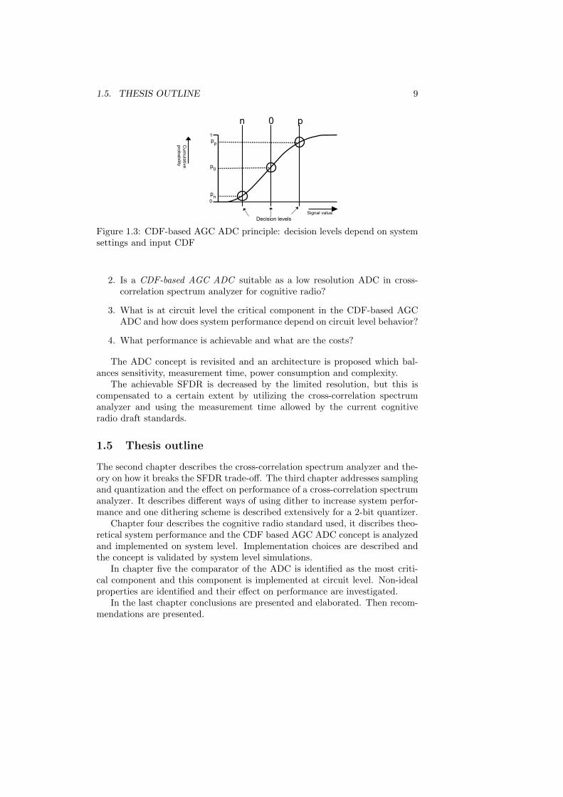
To this end a 2-bit ADC concept originating from ASTRON is investigated[7], [8]. Apart from the low-resolution, it has offset canceling and AutomaticGain Control (AGC). These two features contribute to maximization of systemperformance. The offset canceling and AGC is achieved by variable decisionlevels of the ADC. The decision levels determine the output code of a sample.The value of the decision levels are based on the Cumulative Distribution Func-tion (CDF) of the input signal. The ADC is therefore referred to as CDF-basedAGC ADC. The relation between the input CDF and the reference levels isillustrated in Figure 1.3. The probabilities at the y-axis ([pn, p0, pp]) are set bya system controller, through the cumulative distribution function of the inputsignal the ADC’s decision levels are set.
To investigate the suitability of low resolution ADCs in general and theCDF-based AGC ADC specifically, the following sub-questions are defined:
1. How does spectrum analyzer performance depend on the ADC resolution?
1.5. THESIS OUTLINE 9
Cu
mu
lative
pro
ba
bility
n 0 p
Signal value
1
0
Decision levels
pn
p0
pp
Figure 1.3: CDF-based AGC ADC principle: decision levels depend on systemsettings and input CDF
2. Is a CDF-based AGC ADC suitable as a low resolution ADC in cross-correlation spectrum analyzer for cognitive radio?
3. What is at circuit level the critical component in the CDF-based AGCADC and how does system performance depend on circuit level behavior?
4. What performance is achievable and what are the costs?
The ADC concept is revisited and an architecture is proposed which bal-ances sensitivity, measurement time, power consumption and complexity.
The achievable SFDR is decreased by the limited resolution, but this iscompensated to a certain extent by utilizing the cross-correlation spectrumanalyzer and using the measurement time allowed by the current cognitiveradio draft standards.
1.5 Thesis outline
The second chapter describes the cross-correlation spectrum analyzer and the-ory on how it breaks the SFDR trade-off. The third chapter addresses samplingand quantization and the effect on performance of a cross-correlation spectrumanalyzer. It describes different ways of using dither to increase system perfor-mance and one dithering scheme is described extensively for a 2-bit quantizer.
Chapter four describes the cognitive radio standard used, it discribes theo-retical system performance and the CDF based AGC ADC concept is analyzedand implemented on system level. Implementation choices are described andthe concept is validated by system level simulations.
In chapter five the comparator of the ADC is identified as the most criti-cal component and this component is implemented at circuit level. Non-idealproperties are identified and their effect on performance are investigated.
In the last chapter conclusions are presented and elaborated. Then recom-mendations are presented.


Chapter 2
Integrated cross-correlationspectrum analyzer
The task of an energy detection spectrum analyzer for the use in a cognitiveradio application is to find spectrum holes. The performance of the spectrumanalyzer determines the chance of successfully finding spectrum holes. Whenstrong narrow-band signals are present at the input of a spectrum analyzer,the performance of the spectrum analyzer is limited by its SFDR. The SFDR isincreased by the cross-correlation spectrum analyzer with respect to traditionalspectrum analyzers. This chapter provides insight in the increased performanceof the cross-correlation spectrum analyzer with respect to traditional spectrumanalyzers. The mechanism used by the spectrum analyzer is introduced and thespectrum analyzer itself is described. First the SFDR trade-off is described andthe conventional equation for SFDR is extended with the variable measurementtime. Then cross-correlation is described, starting from a mathematical pointof view and ending with an estimator which can be easily implemented digitally.Then the cross-correlation spectrum analyzer is described. The role of the ADCand the dependency of its cost on word-size is described.
2.1 The SFDR trade-off
A big challenge in cognitive radio spectrum sensing is that the power of verysmall signals should be measured while the overall signal can also contain strongnarrow band signals. This problem can be characterized in terms of the SFDR.SFDR is a performance measure of an analog system. It gives the ratio betweenthe strongest and the weakest signal that can be detected at the same time [9].The SFDR results from the trade-off between linearity and noise. This trade-off can be extended by the factor measurement time by lowering the noise bycross-correlation [4], [5].
The SFDR of a system depends on noise power and non-linearity. Thenoise power added by a system is expressed as the noise factor, which is theratio of input Signal to Noise Ratio (SNR) and output SNR. For most systemsthe noise figure is specified, which is the noise factor expressed in dB. Thenon-linearity is expressed as Input referred third order Intercept Point (IIP3),which is a measure for distortion in a system.
11

12CHAPTER 2. INTEGRATED CROSS-CORRELATION SPECTRUM
ANALYZER
Spurious Free Dynamic Range For an analog front-end the DynamicRange (DR) is defined as the ratio between the noise floor and the maximuminput signal. However, due to non-linearity the maximum attainable dynamicrange can be limited by distortion components. When the strongest distortioncomponent power is equal to the noise floor, the ratio between input signal andthe input referred strongest harmonic is the SFDR. Figure 2.1 illustrates theSFDR for an arbitrary spectrum analyzer.
The noise in Figure 2.1 is white and the magnitude of the noise depends
on the bandwidth in which the noise power is expressed, for instance V 2
kHz . Inthat case the resolution bandwidth is 1kHz.
SFDR
F1Frequency
Magnitude
Noise
F3 F5 F7
Figure 2.1: Spurious free dynamic range
If the IIP3 approximation is acceptable and if the noise floor is white, thenthe SFDR is expressed as [10]:
SFDR =2
3(IIP3− Pnoisefloor − 10 · log10(RBW ) + 174) [dB] (2.1)
Where RBW is the resolution bandwidth and Pnoisefloor is the power of thenoise floor per Hertz. If it is possible to reduce the noise and keep the IIP3unchanged, this trade-off is broken and yields higher SFDR. This is possiblewith cross-correlation.
Noise factor The noise factor (F ) expresses the amount of noise added bya system:
F =SNRoutputSNRinput
(2.2)
When subsystems are cascaded, where block i is followed by block i + 1, con-tributions to the total system noise depends on the gain of the other blocks.The contribution of the subsystems to the noise factor of the total system iscalculated as follows:
Ftotal = 1 + (F1 − 1) +F2 − 1
Ga,1+ ..+
Fm − 1
Ga,1 ·Ga,2..Ga,m−1(2.3)
2.1. THE SFDR TRADE-OFF 13
Where Ga,i are available power gains: the input and output impedances arematched. For unmatched sub-blocks the formula gets more complicated [11, ,pg. 45] but the following effect remains: Noise added in early stages contributemore to total system noise factor, when the gain of the sub-blocks is > 1.
Input referred third order intercept point Most integrated circuits inanalog front-ends are differentially implemented, such that second order dis-tortion is canceled out. For these cases the third harmonic is in general thelargest distortion component. The linearity of a circuit is therefore often ex-pressed in the IIP3, which is the theoretical intercept point of the input referredfirst harmonic power and the input referred power of the strongest distortioncomponent. The strongest distortion component is either the third harmonicof a single pure sine wave, or the component of a 2-tone test which falls in themeasured bandwidth. For narrow-band systems, for the strongest distortioncomponent the strongest distortion component is introduced by aplying twofrequencies such that the
When the non-linearity of a system is modeled as:
y(t) = α0 + α1 · x(t) + α2 · x2(t) + α3 · x3(t)... (2.4)
so when x(t) = A · cos(t) this results in the equation: [11]
y(t) =α2A
2
2+
(α1A
3α3A2
4
)cos(ωt) +
α2A2
2cos(2ωt) +
α3A3
4cos(2ωt)
(2.5)
Because of differential circuitry the even order terms disappear. Because ofsmall values of A, higher powers of A then n for term n can be neglected.
Then the IIP3 is the input power of x(t) for which holds:
var(x(t)) =α3
4 · α1var(x3(t)) (2.6)
This approach uses harmonic distortion components to determine IIP3. Forsmall band systems an approach based on intermodulation of two sine wavescan be used [11].
Real interception of the first and third harmonic does not happen in practicedue to limited gain at large input signal powers. The gain is limited when othernon-linear effects dominate such that Equation 2.4 is not valid anymore, forexample saturation or compression.
When subsystems are cascaded its contribution to the total system noisedepends on the gain of the other sub-blocks. A approximation of the totalsystem IIP3 is [11, pg. 24] :
1
IIP3total=
1
IIP31+
Ga,1IIP32
+ ...+Ga,1 ·Ga,2..Ga,m−1
IIP3m(2.7)
(2.8)
Where IIP3# denote the ratio of first and third signal harmonic powers at alinear scale. Although Equation 2.7 is an approximation the following effectremains: Non-linearity added in later stages contribute more to total systemnon-linearity, when the gain of the sub-blocks is > 1. The effect is the oppositeof the effect of the noise figure in cascaded stages, which is the reason for theSFDR trade-off.
14CHAPTER 2. INTEGRATED CROSS-CORRELATION SPECTRUM
ANALYZER
The trade-off The trade-off between non-linearity and noise in a systemconsisting of cascaded subsystem can be influenced by choosing the locationof the gain. This can be seen in Equations 2.7 and 2.3. When more gain islocated in later stages the noise is increased and IIP3 is reduced.
This trade-off between noise and linearity is broken when a cross-correlationfront-end is used. Such an analog front-end is described in [4]. This front-endconsists of two parallel paths, where the uncorrelated noise floor introduced inboth paths is reduced by cross-correlating the two output signals.
When a cross-correlation front-end is used, the SFDR also depends on mea-surement time. If the amount of correlated noise in the front-end is smallcompared to the amount of uncorrelated noise, then 2.1 changes to:
SFDR ≈ 2
3(IIP3− Pnoisefloor − 10 · log10(RBW ) + 174
+10 · log10(√Tm ·RBW )
) (2.9)
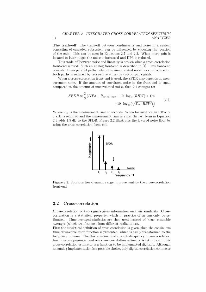
Where Tm is the measurement time in seconds. When for instance an RBW of1 kHz is required and the measurement time is 2 ms, the last term in Equation2.9 adds 1.5 dB to the SFDR. Figure 2.2 illustrates the lowered noise floor byusing the cross-correlation front-end.
SFDR
F1Frequency
Magnitude
Noise
F3 F5 F7
Figure 2.2: Spurious free dynamic range improvement by the cross-correlationfront-end
2.2 Cross-correlation
Cross-correlation of two signals gives information on their similarity. Cross-correlation is a statistical property, which in practice often can only be es-timated. Time-averaged statistics are then used instead of ’true’ ensembleaverages (which are obtained from different realizations).First the statistical definition of cross-correlation is given, then the continuoustime cross-correlation function is presented, which is easily transformed to thefrequency domain. The discrete-time and discrete-frequency cross-correlationfunctions are presented and one cross-correlation estimator is introduced. Thiscross-correlation estimator is a function to be implemented digitally. Althoughan analog implementation is a possible choice, only digital correlation estimator

2.2. CROSS-CORRELATION 15
issues are addressed because an analog implementation would introduce morecorrelated noise sources. Finally, spectral averaging is addressed as a way toactually benefit from the cross-correlation estimation.
2.2.1 Statistical representation
The cross-correlation ρXY of two signals X and Y is the normalized version ofthe cross-covariance [5]:
ρXY (t, τ) =E[(X∗(t)− µX∗(t)
)·(Y (t+ τ)− µY (t+τ)
)]σX(t) · σY (t+ τ)
· (2.10)
Where ∗ denotes the complex conjugate. The scaling factor σX(t) · σY (t +τ) is often not known or assumed 1, making the cross-covariance and cross-correlation equal. In this document the term cross-correlation is used for bothmetrics. The cross-correlation function becomes the auto-correlation functionwhen Y = X in Equation 2.10.
Joint ergodicity of input signals The input signals X and Y are assumedto be jointly ergodic, which means [12]:
1. The signals are wide sense stationary, i.e. their first and second ordermoments are time invariant.
2. Ensemble average and time average are equal: the first and second ordermoments along the time dimension are equal to the first and second ordermoments across the space of different realizations.
2.2.2 Continuous time and frequency representation
Because of the assumed ergodicity of the input signals the result of Equation2.10 can also be obtained by the following time dependent function:
γXY (τ) = limT→∞
1
2T
∫ ∞−∞
x∗(t) · y(t+ τ)dt (2.11)
An important property of the cross-correlation function is that its Fourier trans-form yields the cross-power spectrum:
ΓXY (f) = F (γXY (τ)) (2.12)
ΓXY (f) =
∫ ∞−∞
γXY (τ)e−j2·πfτdτ (2.13)
(2.14)
Convolution and cross-correlation are very similar:
x(t) ∗ y(t) =
∫ ∞−∞
x(τ) · y(τ − t)dτ (2.15)
x(t) ? y(t) =
∫ ∞−∞
x∗(τ) · y(τ + t)dτ (2.16)
x(t) ? y(t) = x∗(−t) ∗ y(t) (2.17)
16CHAPTER 2. INTEGRATED CROSS-CORRELATION SPECTRUM
ANALYZER
Where ? denotes the cross-correlation operation and ∗ denotes convolution.Because convolution in the time domain is multiplication in frequency domain,the cross power spectrum of signals x and y is:
ΓXY (f) = X∗(f) · Y (f) (2.18)
where X(f) and Y (f) are the spectra of x and y respectively, obtained via theFourier transform:
X(f) = F (x(t)) (2.19)
Y (f) = F (y(t)) (2.20)
2.2.3 Discrete-time and -frequency representation
A discrete-time version of the above described cross-correlation function exists.The input signal is sampled with frequency fs. The estimated cross-correlationfunction then becomes:
rXY (n) = limM→∞
1
2 · (M + 1)
M∑m=−M
x∗(m) · y(m+ n) (2.21)
(2.22)
Analogous to the continuous time case, the discrete-time cross-correlation func-tion can be converted to the frequency domain by the discrete-time FourierTransform:
RXY (f) = F (rXY (n)) (2.23)
RXY (f) =
∞∑n=−∞
rXY (n) · e−j2πffsn (2.24)
When the result of this transform is estimated by a digital system, a discrete-frequency representation is required. This is obtained by applying a discreteFourier transform (DFT):
RXY (k) = DFT (rXY (n)) (2.25)
RXY (k) =
N−1∑n=0
rXY (n) · e−j 2πN nk (2.26)
Again analogous to the continuous case, the cross-power spectrum can alsobe obtained by the product of the conjugate spectrum of x(n) and the spectrumof y(n):
RXY (k) = X∗(k) · Y (k) (2.27)
For a practical implementation this function has to be estimated. There aredifferent estimators of the discrete cross-correlation function found in literature[12], of which two are widely used: the biased estimator and the unbiasedestimator [5]. The unbiased estimator yields larger mean-square error. Thebiased estimator is focused on and is described in Section 2.2.4. Under plausibleassumptions both estimators give comparable performance, so choosing one orthe other is does not make a difference. For detailed information, see [5].

2.2. CROSS-CORRELATION 17
2.2.4 Estimation of the discrete-time and -frequencycross-correlation function
The estimator for cross-correlation is described in discrete-time and discrete-frequency domain in following paragraphs.
Time domain cross-correlation estimator When the summing intervalof Equation 2.21 is reduced to a realistic value, a biased estimator appears.When samples are available for 0 < n < N − 1 and all other samples are setzero, the summation interval reduces to 0 < n < N − 1:
cXY (k) =1
N
N−1∑n=0
(x∗(n) · y(n+ k)) (2.28)
(2.29)
The estimator gives output values for (−N + 1) < k < (N − 1). For large |k|a relatively small number of products is available. The estimation is then lessaccurate because the factor 1
N does not correspond to the number of availableproducts. This error is referred to as the estimator bias and is described in [5].When N is large with respect to k, the bias is small and as N goes to infinity thebias converges to zero. The estimated cross-power spectrum is now obtainedby Discrete Fourier transforming cXY :
CXY = DFT (cXY ) (2.30)
Obtaining the cross-power spectrum by correlation prior to Fourier trans-formation is referred to as XF correlation.
Frequency domain cross-correlation estimator The frequency domainversion of the estimator calculates the spectra of parts of signal x(m) and y(m)and multiplies them:
X(f) =
∞∑n=−∞
x(n) · e−j 2πN nf (2.31)
Y (f) =
∞∑n=−∞
y(n) · e−j 2πN nf (2.32)
CXY = X∗(f) · Y (f) (2.33)
Obtaining the cross-power spectrum by discrete Fourier transformationprior to correlation is referred to as FX correlation.
2.2.5 Auto-correlation, Cross-correlation and spectrumestimation
In traditional spectrum analyzers the Power Spectral Density (PSD) is a re-sult of auto-correlation and is equal to the cross-correlation front end whenno uncorrelated components are present in the input signals. When two sig-nals x(t), y(t) are composed of correlated components s(t) and uncorrelated

18CHAPTER 2. INTEGRATED CROSS-CORRELATION SPECTRUM
ANALYZER
components u1(t), u2(t), their cross-correlation function is:
γXY (t) = limT→∞
1
2T
∫ ∞−∞
x∗(τ) · y(t+ τ)dτ (2.34)
= limT→∞
1
2T
∫ ∞−∞
(s(τ) + u1(τ))∗ · (s(t+ τ) + u2(t+ τ))dτ (2.35)
= γss(t) + γsu2(t) + γu1s(t) + γu1u2
(t) (2.36)
= γss(t) (2.37)
And thus the resulting power spectrum converges to the power spectrum ofs(t).
When multiple spectra of the cross-correlation front-end are averaged, thecorrelated components of the two input signals converge to their actual valuesand the uncorrelated components of the input signals converge to zero.
Power spectrum variance Due to randomness of noise and limited mea-surement time, the noise floor in an estimated spectrum is not the same indifferent measurements. For Gaussian distributed noise the distribution of thenoise PSD components is also Gaussian. To express the noise floor, the stan-dard deviation of the power spectrum components is used.
Noisefloor = σPSDn =√var(PSDn) (2.38)
where PSDn denotes the PSD of the noise. In order to estimate the noisefloor in auto- and cross-power spectra, the mean and standard deviation of thesignal’s PSD must be estimated.
For the variance of the cross-power estimator in Equation 2.33, the varianceof the estimated cross-power spectrum converges to the squared cross-powerspectrum of signals x and y [5]. In other words, as the measurement timeincreases, the variance per Hertz does not decrease:
limN→∞
var(CXY (f)) = |ΓXY (f)|2 (2.39)
As the variance of the signal does not converge to zero, the estimation outputdoes not converge to the value being estimated. The variance per resolutionbandwidth remains constant: The estimator is inconsistent. To get a consistentcross-power spectrum estimator, spectral averaging is applied.
Spectral averaging Spectral averaging is applied to the output of the cross-correlation estimation to reduce the variance per resolution bandwidth suchthat it results in a consistent estimation. There are several methods of spectralaveraging, the method described below is the Bartlett-method (also used forthe cross-correlation spectrum analyzer of the previous work). The Bartlett-method splits a measurement in L sequences of length K and averages thespectra of those sequences.
CXY (f) =1
L·L∑l=0
(Xl(f) · Y ∗l (f)) (2.40)

2.2. CROSS-CORRELATION 19
For the true cross-power spectrum, the spectral variance reduces when themeasurement time is increased and the cross-power spectrum will converge tothe power spectrum of its correlated signal components:
var(ΓXY ) =1
Lvar (Γss + Γsu2 + Γu1s + Γu1u2) (2.41)
The noise floor standard deviation thus decreases by the square root of therelative increase in measurement time.
σ(ΓXY ) =
√1
L
√σ(Γss) + σ(Γsu2 + Γu1s + Γu1u2) (2.42)
The reduction of spectral variance of the cross-power spectrum is approximatelyequal to the reduction of spectral variance of the estimated spectrum:
σ(CXY ) ≈√
1
L
√σ(Css) + σ(Csu2
+ Cu1s + Cu1u2) (2.43)
because:
ΓXY ≈ CXY (2.44)
When a cross-spectrum is averaged, its components converge to their actualvalues: the variance is reduced. For an uncorrelated signal, the cross-spectrumpower is 0, so according to Equation 2.42 the uncorrelated components decrease
by√
1L . So as a rule of thumb, the standard deviation of the noise floor in a
power spectrum decreases by 1.5 dB per doubling of measurement time. Thisin contrast to auto-correlation, where the mean of the noise floor is non-zeroand the absolute noise floor converges to that mean. Figure 2.3 depicts a blockdiagram of a cross-correlation spectrum averaging front-end.
Figure 2.3: Block diagram of the operation of a cross-correlation spectrumaveraging front-end. [4]
Auto-correlation and Cross-correlation spectrum For autocorrelation,X and Y in Equation 2.42 are equal. This results in a sequence of absolute real

20CHAPTER 2. INTEGRATED CROSS-CORRELATION SPECTRUM
ANALYZER
values. The expected value is non-zero and thus the noise floor converges toa non-zero value. Figure 2.4 illustrates the convergence of an auto-correlationspectrum to its expected value. For cross-correlation, X and Y in Equation 2.42are unequal. This results in a sequence of complex values. The expected valueis zero if the noise signals are fully uncorrelated and the noise floor convergesto zero. Figure 2.4 illustrates the convergence of a cross-correlation spectrumto its expected value.
−4 −2 0 2 40
1−4
−2
0
2
4
Imagf/fs
Rea
l
−4 −2 0 2 40
1−4
−2
0
2
4
Imag
aver
aged
:1x
f/fsR
eal
0 0.5 10
1
2
3
4
f/fs
Mag
nitu
de
0 0.5 10
1
2
3
4
f/fs
Mag
nitu
de
−4 −2 0 2 40
1−4
−2
0
2
4
Imag
aver
aged
:5x
f/fs
Rea
l
−4 −2 0 2 40
1−4
−2
0
2
4
Imagf/fs
Rea
l
0 0.5 10
1
2
3
4
f/fs
Mag
nitu
de
0 0.5 10
1
2
3
4
f/fsM
agni
tude
−4 −2 0 2 40
1−4
−2
0
2
4
Imag
aver
aged
:50x
f/fs
Rea
l
−4 −2 0 2 40
1−4
−2
0
2
4
Imagf/fs
Rea
l
0 0.5 10
1
2
3
4
f/fs
Mag
nitu
de
0 0.5 10
1
2
3
4
f/fs
Mag
nitu
de
complex spectrum complex spectrumabsolute spectrum absolute spectrum
Auto-correlation Cross-Correlation
Figure 2.4: Convergence of power spectra when spectrum averaging is applied.

2.3. CROSS-CORRELATION SPECTRUM ANALYZER 21
2.3 Cross-correlation spectrum analyzer
This section describes the specific front-end which is used in the previous work[4] and on which assumptions and system calculations are based. First anFFT spectrum analyzer is described and then the cross-correlation spectrumanalyzer is described. The latter can be seen as an extension to the FFTspectrum analyzer.
2.3.1 FFT spectrum analyzer
The FFT spectrum analyzer obtains spectrum information by Fast-Fourier-Transforming the input signal. The input signal is first filtered, amplifiedand down-mixed before it is converted to the digital domain where the FFTis calculated. Figure 2.5 shows a block diagram of this front-end. (In thisfigure the noise floor is a bit exaggerated to emphasize the benefit of the cross-correlation spectrum analyzer in following figures).
A
D
LO
LNA FFTLPF
Figure 2.5: Typical analog front-end
By choosing the mixing frequency, the Intermediate Frequency (IF) bandcan be selected. A number of possible ranges are identified, each having theiradvantages. In the following sections zero-IF range is elaborated, as it is used inprevious work and allows the largest bandwidth to be converted to the digitaldomain.
2.3.2 Cross-correlation spectrum analyzer
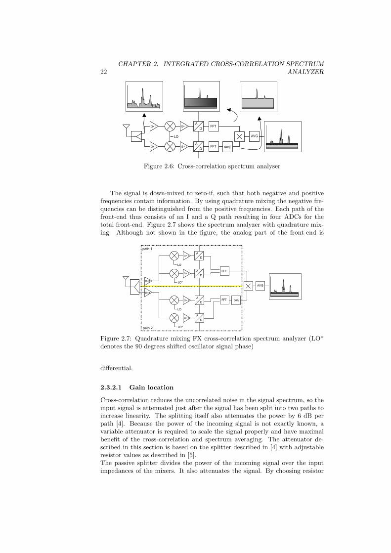
The cross-correlation spectrum analyzer consists of two FFT spectrum ana-lyzers placed in parallel. The FFT outputs are cross-correlated and averaged.It consists of a passive splitter to divide the signal power over the two sig-nal paths. Because of the noise-linearity trade-off described in section 2.1 thesignals are not amplified by Low Noise Amplfiefiers (LNA) but attenuated inboth paths. Both signals are then down-mixed to zero-IF and converted to thedigital domain by the ADCs. The digital section consists of two Fast FourierTransform blocks, one of the results is conjugated and the two spectra aremultiplied element-wise. Multiple spectra are then averaged. Figure 2.6 showsa simple representation of the spectrum analyzer. The increased noise floor,due to the lack of LNAs, will be reduced when the output signals are cross-correlated. The theory from section 2.2 can be applied to this front-end. Theeffect of uncorrelated noise sources such as thermal noise from the mixer, ADCand attenuators is reduced in the power spectrum. The noise added by theattenuators is partially correlated [6], so the correlated noise originates fromthe antenna, the passive splitter and attenuator.
In Figure 2.6 the uncorrelated noise power is represented by the gradient-filled areas and is reduced in the final spectrum. The correlated noise power isrepresented by the solid-filled gray area and is not reduced.
22CHAPTER 2. INTEGRATED CROSS-CORRELATION SPECTRUM
ANALYZER
A
DFFT
A
DFFT
AVG
G< 1
G< 1
G> 1
G> 1
LO
conj
Figure 2.6: Cross-correlation spectrum analyser
The signal is down-mixed to zero-if, such that both negative and positivefrequencies contain information. By using quadrature mixing the negative fre-quencies can be distinguished from the positive frequencies. Each path of thefront-end thus consists of an I and a Q path resulting in four ADCs for thetotal front-end. Figure 2.7 shows the spectrum analyzer with quadrature mix-ing. Although not shown in the figure, the analog part of the front-end is
A
D
FFT
A
D
FFT
AVG
G> 1
G> 1
LO*
conj
A
D
A
D
G> 1
G> 1
LO
G<1
G<1
LO*
LO
path 1
path 2
Figure 2.7: Quadrature mixing FX cross-correlation spectrum analyzer (LO*denotes the 90 degrees shifted oscillator signal phase)
differential.
2.3.2.1 Gain location
Cross-correlation reduces the uncorrelated noise in the signal spectrum, so theinput signal is attenuated just after the signal has been split into two paths toincrease linearity. The splitting itself also attenuates the power by 6 dB perpath [4]. Because the power of the incoming signal is not exactly known, avariable attenuator is required to scale the signal properly and have maximalbenefit of the cross-correlation and spectrum averaging. The attenuator de-scribed in this section is based on the splitter described in [4] with adjustableresistor values as described in [5].The passive splitter divides the power of the incoming signal over the inputimpedances of the mixers. It also attenuates the signal. By choosing resistor

2.3. CROSS-CORRELATION SPECTRUM ANALYZER 23
values of the passive splitter, the attenuation can be set. Figure 2.8 shows thedifferential passive splitter.
2Zmixer
2Zmixer
2Rb 1
2
R s 1R s3
R s 2
R s o u rc e
V s o u rc e
R c 2R a 2
R c1R a 1Vx+
Vy+
R a 1 R c 1
R c2R a 2R s1 R s3
R s2
Vy-
Vx-
1 :1
Balun
Splitter 2
Splitter 1
2Rb
Vs,a
Figure 2.8: Passive splitter [6]
The splitter (Rs1 to Rs3) together with the attenuator Rai , Rbi , Rci allowsto attenuate the signal and control the system IF bandwidth [5].
The attenuation of the signal before the mixer reduces the amount of distor-tion produced by the mixer. For proper conversion to the digital domain, thesignal must be scaled to fit the ADC input range. The signal is thus amplifiedbefore the ADC conversion.
2.3.2.2 XF and FX correlation spectrum analyzer
As described in Section 2.2.4 the cross-power spectrum can be estimated in twoways: using an FX- or an XF cross-correlation spectrum analyzer. Until thisparagraph the front-end illustrations show spectrum analyzers where the signalis transformed to a discrete spectrum prior to the cross-correlation. Figure 2.9shows the XF correlation spectrum analyzer.
A
D
A
D
FFT AVG
G> 1
G> 1
LO*
A
D
A
D
G> 1
G> 1
LO
G<1
G<1
LO*
LO
path 1
path 2
cXY
Figure 2.9: Quadrature mixing XF cross-correlation spectrum analyzer (LO*denotes the 90 degrees shifted oscillator signal phase)
2.3.2.3 Cost of the ADC and digital back-end
The cost of a spectrum analyzer is partially determined by the ADCs and thedigital back-end. The cost in this context is power consumption and required

24CHAPTER 2. INTEGRATED CROSS-CORRELATION SPECTRUM
ANALYZER
silicon area. Following paragraphs discuss the dependency of cost on digitalsignal resolution.
ADC The cost of an ADC depends on topology, sample frequency and resolu-tion. When the resolution is lowered the number of comparisons per conversionis reduced and thus the power per conversion is reduced. Reduction of resolu-tion decreases complexity in a way which depends on the topology of the ADC.A flash ADC for instance consists of a comparator for each , the number ofcomparators is reduced and therefore the amount of silicon area is reduced.
Digital back-end For the digital back-end, a higher sampling frequencyleads to more dynamic power consumption, because parasitic capacitances arecharged and discharged more often [13]. Higher resolution leads to more digitallogic and thus to more parasitic capacitances and more silicon area. When thedependency of cost on resolution is considered, the digital implementation be-comes important. For the cross-correlation spectrum analyzer the dependenceof cost on resolution may be different for a FX or a XF correlation. When theXF correlator is used, the digital signals are correlated just after the analog todigital conversion. The signal resolution is determined by the resolution of theADC. When the output of the correlator is transformed to a discrete spectrum,the signal resolution is determined by the desired sensitivity of the spectrumanalyzer. For a lower resolution, the reduction of cost is clearly located in theXF correlator.
When the FX correlator is used, the lower resolution also leads to costreduction. The FFT modules have low resolution input signals and high res-olution output signals. The resolution of internal nodes will increase as thesignal travels trough the FFT module. The exact reduction of cost is less obvi-ous than in the XF correlator case. Also, to compare the cost the time-domaincorrelator cost must be compared to the frequency-domain correlator. Moreinformation on both and other correlators can be found in [5] and [14]
2.4 Summary and conclusions
Summary The cross-correlation spectrum analyzer increases the SFDR byadding the factor measurement-time to the trade-off between noise and lin-earity. Cross-correlation is a statistical property which can be estimated indiscrete-time and discrete-frequency domain. The latter is done by the cross-correlation spectrum analyzer. This spectrum analyzer attenuates the inputsignal to reduce non-linearity introduced by the mixer. After the mixer the sig-nal is amplified to meet the ADC input range before conversion to the digitaldomain. In the digital domain the spectrum estimate is calculated. The powerand silicon-area cost of the digital processing largely depend on the input signalword-size.
Conclusions Cross-correlation is an effective way to increase the SFDR of aspectrum analyzer when the noise power per spectrum bin limits SFDR. Noisepower added in the parallel paths of a cross-correlation spectrum analyzer isreduced at the cost of measurement time. The mixer in the analog front-endintroduces distortion, which is reduced when the signal is attenuated prior to

2.4. SUMMARY AND CONCLUSIONS 25
entering the mixer. At the output of the mixer, an amplifier is required toscale the signal for proper AD conversion Reduction of ADC resolution willclearly reduce the digital complexity in the case of the XF correlator. For anFX correlator it is less straight-forward to determine the complexity reduction.


Chapter 3
Low resolution analog to digitalconversion
In the previous chapter the concept of cross-correlation estimation and thecross-correlation spectrum analyzer are introduced. When the cross-correlationspectrum analyzer is integrated on chip, a low-cost ADC is preferred. Thecost of ADCs can be reduced considerably by reducing the resolution. A low-resolution ADC will consume less power and occupy less chip area in contrastto higher resolution ADCs. Quantization is a non-linear function. The IIP3of a quantizer largely depends on its resolution. Reduction of ADC resolutionresults in increase of the non-linearity. When the resolution is decreased toomuch, the SFDR of the spectrum analyzer is degraded to an unacceptablelevel. A possible counter measure to the non-linearity is to deliberately addnoise to the input signal (dithering the input signal). The effect of lowering theresolution of an ADC is described by first describing the effect of quantizationin general. Then the effects of low-resolution quantization and dithering aredescribed. Different dithering approaches exist, of which one is described moreextensively, as it is implemented on system level for this thesis (see Chapter4).
3.1 Analog to digital conversion
Converting a signal from the analog domain to the digital domain consists oftwo orthogonal operations: quantization and sampling. Figure 3.1 shows thetwo operations. The order in which they are executed does not affect the result.
3.1.1 Sampling
Sampling converts a continuous-time signal to a discrete-time signal. At asingle moment per period, the input signal is represented by a dirac pulse witha strength proportional to the input signal at that moment. In the ideal casethese moments are spaced uniformly. When the Nyquist criterion is satisfied[15], the original signal can be reconstructed from the sampled signal and noinformation is lost.
27

28CHAPTER 3. LOW RESOLUTION ANALOG TO DIGITAL
CONVERSION
Time
Amplitude
Time
Amplitude
TimeAmplitude
Time
Amplitude
Quantization Quantization
Sampling
Sampling
Figure 3.1: Analog to digital conversion: Sampling and Quantization
3.1.2 Quantization
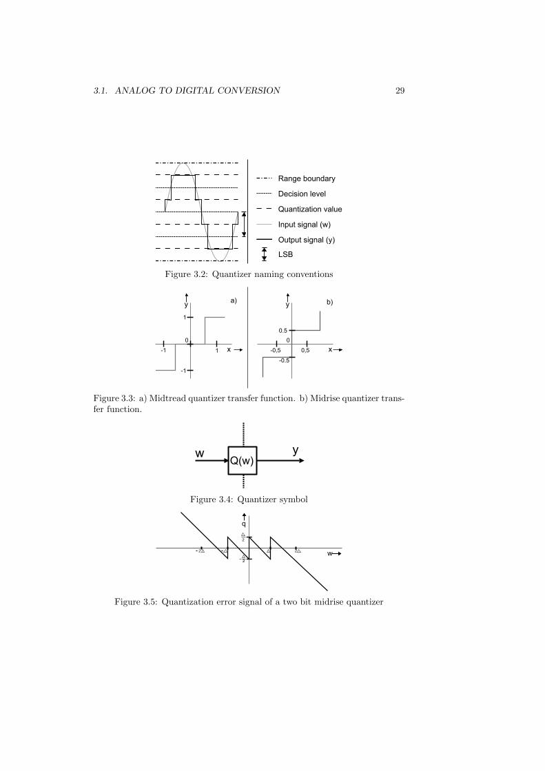
A digital signal is described by a finite set of values. A quantizer rounds theanalog signal to the nearest digital representation. In practice this means thatthe input signal is compared to decision levels to determine the digitized out-put. The possible quantizer output values are referred to as quantization values.The space between two decision levels is called the Least Significant Bit (LSB).Figure 3.2 illustrates the naming conventions. Quantization approaches existwhere the decision levels are not located at equal distance, but for this thesisonly quantizers with uniformly spaced decision levels are described. This typeof quantization is referred to as uniform quantization.
There are two types of quantizers: midtread and midrise quantizers. Figure3.3 shows a part of the transfer function of a midtread and a midrise quantizer.
The description in following sections apply to a quantizer of type midrise,which is used in this thesis because the midrise quantizer is symmetrical aroundzero. (the formulas have obvious analogs for midtread quantizers and all con-clusions are also valid).
The symbolic representation of a quantizer is shown in Figure 3.4. Theoutput of a midrise quantizer is given in Equation 3.1. In this equation therounding is realized by applying the floor operator to the normalized input andadding a half LSB after scaling the result to an LSB:
y = Q(w) = ∆ ·⌊w
∆
⌋+
∆
2(3.1)
where
• w: the input signal to the quantizer
• Q(w): The quantization operation on input signal w
• ∆: The spacing between decision levels: an LSB
And the following is defined:
• q = Q(w)− w: The quantization error.
3.1. ANALOG TO DIGITAL CONVERSION 29
Range boundary
Decision level
Quantization value
Input signal (w)
Output signal (y)
LSB
Figure 3.2: Quantizer naming conventions
0
1
-1
y
x1-1
0
0.5
y
x-0,5 0,5
-0.5
a) b)
Figure 3.3: a) Midtread quantizer transfer function. b) Midrise quantizer trans-fer function.
wQ(w)
y
Figure 3.4: Quantizer symbol
2
w
q
2
22
Figure 3.5: Quantization error signal of a two bit midrise quantizer

30CHAPTER 3. LOW RESOLUTION ANALOG TO DIGITAL
CONVERSION
3.1.2.1 Quantization error
The quantization error q is the difference between the quantizer input andoutput. Figure 3.5 shows the quantization error as a function of the quantizerinput w of a 2-bit quantizer. When the input signal is outside the input rangeof the ADC, the error signal is referred to as clipping error. This type of error isnot addressed in this thesis, but conditions are obtained such that the influenceis limited when the error is unavoidable. Detailed analysis of this type of erroris found in [16].
Distortion Each input signal value has one quantization error value associ-ated with it: i.e. for a given input signal, the quantization error is a deter-ministic signal. As a result the quantization error signal is correlated with theinput signal. This correlation is inversely propertional to the resolution of thequantizer. When the input signal is periodic, the quantization error signal isperiodic and will give distortion components in the output signal spectrum. Inthe spectrum of the distorted signal, harmonic distortion and inter-modulationproducts appear.
For instance when the input to the quantizer is a sine wave with frequencyf , the output spectrum will contain frequency components at multiples of f .Figure 3.6 shows the quantization of a sine wave, the quantization error hasdistinct frequency components with higher frequencies.
0 50 100 150−0.5
0
0.5Quantization of sine wave
Samples
Am
plitu
de
Input signal
Output signal
Decision level
0 50 100 150−0.2
−0.1
0
0.1
0.2
Samples
Am
plitu
de
Total error �
0 0.1 0.2 0.3 0.4 0.5−60
−50
−40
−30
−20
−10
0
Quantized signal spectrumSFDR: 17.8753[dB]
s
Mag
nitu
de[d
B]
Frequency [f ]
Figure 3.6: 2-bit Quantization of a sine wave and the quantization error.
For a uniform quantizer, based on a full scale sine wave input, the SFDR is[17]:
SFDR ≈ 8.07 ·D + 3.29 (3.2)
where b is the number of bits of the quantizer.
3.1.3 Models of quantization
There are different ways to look at quantization. A simplistic view is theclassical model of quantization, which linearizes the quantization operation [18].Another vies is to analyze the effect of non-linearity. Blachman describes anapproach to calculate distortion components [19]. In practical situations noiseis present which improves the SFDR. This improvement in SFDR is exploitedwhen the signal is dithered. Dithering is deliberately adding a noise signal tothe input signal to control distortion components.

3.1. ANALOG TO DIGITAL CONVERSION 31
3.1.3.1 Classical model of quantization
The classical model of quantization [18] approximates the effects of quantizationby assuming that the quantization noise is uncorrelated with the input signal,has a white spectrum and is uniformly distributed. The result of quantizationis then easily described by white noise added to the input signal. The power ofthe quantization error is [20] a function of its Probability Distribution Function(PDF) (pq(q)):
pq(q) =1
∆, for
−∆
2< q <
∆
2(3.3)
(3.4)
such that the power is:
E(q2) =
∫ ∆2
−∆2
q2 · pq(q)dt =∆2
12(3.5)
3.1.3.2 Spectrum of quantized signals
The exact magnitude and phase of distortion components can be calculatedwith the method described in [19]. The quantization error for a single sine waveinput is expressed by its Fourier series [19]. The mathematical derivations arefound in [19] for a midtread quantizer. The modification to this derivation fora midrise quantizer can be found in Appendix A. The result is:
w = A · sin(θ(t)) (3.6)
q(w) =
∞∑p=1,3,5,7,...
( ∞∑n=1
2
πnJp(2π · n ·A)sin(p · θ(t))
)(3.7)
where Jp(2π · n ·A) is the Bessel function of the first kind.When the input signal is a sum of multiple sine waves, the number of
distortion components increases exponentially. As an example, the Fourierseries for two sine waves is obtained by extending the approach of [19]:
w = A1 · sin(θ1(t)) +A2 · sin(θ2(t)) (3.8)
q(w) = imag {∞∑
p=−∞
∞∑q=−∞
( ∞∑n=1
1
nπJp(2π · n ·A1) · ei p θ1 ·
Jq(2π · n ·A2) · ei q θ2)}
(3.9)
If the input signal remains within the quantizer input range, the expected
quantization error power cannot exceed(
∆2
)2, as the error has a maximum
value of ∆2 . The number of distortion components in the spectrum increases
exponentially with respect to the number of sinusoids at the input, so thepower per distortion component decreases: adding more frequency componentsreduces the average power per distortion frequency component. When whitenoise is added this effect is maximally utilized, because it contains an infinite

32CHAPTER 3. LOW RESOLUTION ANALOG TO DIGITAL
CONVERSION
number of sinusoids. How well the power of the quantization error is dis-tributed across the spectrum depends on the amount of power of the whitenoise and whether it is statistically independent of the input signal. As aconclusion, adding white noise to the signal is an effective way to decreasedistortion components and thus increase linearity. Adding a signal to reducedistortion components is known as dithering.

3.2. DITHER 33
3.2 Dither
Quantization of a signal is a non-linear process which adds undesired distor-tion and inter-modulation components to the signal. Dithering is a processapplied to the signal before the non-linear operation to control these undesiredcomponents. In many applications dithering adds a random signal to an inputsignal.
For energy detection spectrum sensing the power and spectral distributionof the dither signal and quantization noise must be known, such that signalpower can be distinguished from the noise power. This is achieved when theADC generates an error with a white spectrum. The noise floor of the out-put signal is then also white. This is achieved by dithering the input to thequantizer.
This section discusses different dithering schemes. Each scheme has itsadvantages and disadvantages and its suitability depends on the application itis used in. First dithering is explained intuitively.
3.2.0.3 Dither, intuitive approach
Without dithering, an input value can result in only one error value, so when theinput signal is periodic the quantization error signal is periodic. The periodicitywould not be present when an input value could result in any quantizationerror with equal probability. This is achieved with proper dithering. Figure3.7 shows that the periodicity of the error signal is not present when a sinewave is dithered with uniform distributed dither with a range of 1 LSB. Withthis kind of dither each quantization error value is equally probable.
0 50 100 150−0.4
−0.2
0
0.2
0.4Quantization of sine wave
Samples
Amplitude
Input signal
Output signal
Decision level
0 50 100 150−0.2
−0.1
0
0.1
0.2
Samples
Amplitude
Total error
0 50 100 150−0.5
0
0.5
Quantization of ditheredsine wave
Samples
Amplitude
Input signal
Output signal
Decision level
0 50 100 150−0.2
−0.1
0
0.1
0.2
Samples
Amplitude
Total error dithered quantizer
0 0.1 0.2 0.3 0.4−60
−50
−40
−30
−20
−10
0
Quantized signal spectrumSFDR: 17.5716[dB]
Relative frequency [1/fs]
Mag
nitude
[dB]
0 0.1 0.2 0.3 0.4−60
−50
−40
−30
−20
−10
0
Quantized signal spectrumSFDR: 21.5672[dB]
Relative frequency [1/fs]
Mag
nitude
[dB]
Figure 3.7: Quantized undithered and dithered sine wave with an amplitudeof 3
4 full scale, the error signal and spectrum. The spectrum of the unditheredsignal only contains odd harmonics of the fundamental frequency, the spectrumof the dithered signal also has frequencies at even harmonic frequencies.

34CHAPTER 3. LOW RESOLUTION ANALOG TO DIGITAL
CONVERSION
3.2.1 Dithering schemes
Many different dithering schemes can be found in literature [18], [21], [22], [23].The most important differences between the schemes are:
1. Subtractive or non-subtractive dither
2. Type of dither signal PDF
3. Bandwidth of the dither signal
The advantages and disadvantages of these differences are described. At theend of this section the approach is selected which fits the goals of this thesisbest.
3.2.1.1 Subtractive or non-subtractive dither
Adding dither to the input signal decreases distortion components, but thequantized signal also contains the dither signal. Figure 3.13 shows the blockdiagram of a non-subtractive dithered quantizer.
DitherGenerator
yxv
w Q(w)
Figure 3.8: Dithered quantizer
In subtractive dithering the dither signal power is removed from the quan-tizer output signal by subtracting a digital version of the dither signal from thequantizer output signal. In [24] the concept of subtractive dither is introduced.In this paper digital images are dithered and quantized before they are trans-mitted over a channel with limited capacity, then after reception the dither issubtracted. This way the bandwidth of the transmitted signal can be reducedwhile the distortion in the image is acceptable. Figure 3.9 shows a subtractivedithered quantizer.
vAD
DitherGenerator
x y
DA
vAD
DitherGenerator
x y
AD
a) b)
Figure 3.9: Subtractive dither quantizer. The dither source can be in: a) digitalor b) analog domain.

3.2. DITHER 35
For a spectrum analyzer subtractive dithering leads to an increase of digitalresolution just after the quantization, so the benefit from resolution reductionof the ADC is decreased when the dither is subtracted. I.e. the resolutionreduction leads to only little complexity reduction as the digital processingcomplexity is not reduced. The ADC resolution is reduced, but not the digitalword resolution. However, because the ADC resolution is lowered, this may stillbe a interesting option. Comparing non-subtractive dithering to subtractivedithering; the latter results in less noise power, but the first achieves morecomplexity reduction.
3.2.1.2 Type of dither signal
Most natural noise sources produce signals with an amplitude which has aGaussian distributed PDF. For instance, the voltage and current amplitude ofthe thermal noise of a resistor is Gaussian distributed. However, dither signalswith other specific PDFs lead to a higher SFDR.
Gaussian distributed noise In [17] the effect of Gaussian distributed noiseis analyzed. Adding a Gaussian distributed noise signal increases the SFDR,Equation 3.2 is extended to:
SFDR ≈ 8.07 ·D + 3.29 + 171.5 · σ2LSB (3.10)
where σ2LSB is the power of the noise in LSB2. This might look very promis-
ing, however two performance limiting effects are introduced when increasingGaussian distributed dither signal power:
1. The noise floor is raised.
2. Signal values falling outside the quantizer input range introduce clippingdistortion.
The clipping distortion problem is reduced by attenuating the input signal,but the noise floor becomes more dominant and the SFDR is reduced. Figure3.10 shows the dithered quantizer with attenuated input signal.
DitherGenerator
yv
Q(w)w
<1x
Figure 3.10: Dithered quantizer with attenuated input signal.
In [17] the allowed probability of a value being clipped is coarsely estimated.According to this estimation, for an 8-bit quantizer, the probability of clippedvalues must be less than 0.13 % to have no discernible distortion. For lowerresolutions, for example 2 bits, the resulting distortion and required attenuationresults in unacceptable SFDR values. The estimation of [17] does not correctlyapproximate the allowed clipping for a 2-bit quantizer when the target SFDRis 60 dB. This is concluded from simulation results. Time domain simulations

36CHAPTER 3. LOW RESOLUTION ANALOG TO DIGITAL
CONVERSION
in MATLAB show the relation between Gaussian distributed noise power andrequired attenuation of the input signal to allow a certain SFDR. The result ofthis simulation is shown in Figure 3.11. The SFDR is obtained for an amountof noise power and a certain amplitude of the sine wave input. The amount ofnoise power results from equation 3.10:
σ2LSB =
SFDRtarget − 3.29− 8.07 ·D171.5
(3.11)
For a SFDR of 60 dB the input signal must be attenuated by 20 dB, relativeto a full scale sine wave. The amount of dither power is roughly equal tothe dithering alternatives of next paragraphs, thus the resulting dither andquantization noise floor is roughly equal. However, the 20 dB attenuationmakes this dithering option not attractive.
20
30
40
50
60
−20−15
−10−5
0
10
20
30
40
50
60
Input signal [dBFs]
SFDR [dB]
target
Ach
ieva
ble
SFD
R[d
B]
Figure 3.11: Achievable SFDR for Gaussian distributed dither and signal at-tenuation. MATLAB code snippet can be found in Appendix C.2.
Non-Gaussian distributed noise Dither signals with other distributionslead to less required signal attenuation and a fixed amount of noise power.Finding a signals with specific distributions in the analog domain is not trivial,therefore the dither signal is generated in the digital domain and then convertedto the analog domain by a Digital to Analog Converter (DAC), this is illustratedin Figure 3.9.b. Section 3.3 elaborates these types of dither signals extensively,the required signal attenuation is 2.5 dB or 6 dB depending on the exact dithersignal.
3.2.1.3 Bandwidth of the dither signal
A dither signal can have a bandwidth which is a fraction of the measurementbandwidth. This is referred to as band-limited dither or narrow-band dither.When the used dither signal has a bandwidth equal to the measurement band-width, this is referred to as wide-band dithering. When the dither signal bandis only a part of the measured band, the other part of the band does not sufferfrom higher noise power levels. This might sound promising, but generationof band-limited dither with a specific non-Gaussian PDF is difficult or may be

3.2. DITHER 37
impossible. The signal must be for instance uniformly distributed (see section3.3.1.2 for more details). When a white signal with a uniform PDF is filtered,the resulting PDF becomes more Gaussian like. This can be explained bythe fact that filtering is summing time delayed versions of the same white sig-nal, which is adding multiple independent signals with a uniform distribution.The creation of band-limited dither signals with specific PDF requirements isconsidered out of scope of this thesis and is not further investigated.
Figure 3.12 illustrates the principle of subtractive, non-subtractive andband-limited dithering: non-subtractive dither increases SFDR, but it is lim-ited by the increased noise floor. Subtractive dither results in a lower noisefloor. In the case of band-limited dither a part of the spectrum is dedicatedfor the dither signal power.
SFDR
F Ffundamental Largest spur
Frequency
Magnitude
Disto
rtion Dither
SFDR
Ffundamental
Frequency
Magnitude
Distortion
SFDR
Ffundamental
Frequency
Magnitude
DistortionDither
SFDR
Ffundamental
Frequency
Magnitude
Distortion
a) b)
c) d)
Figure 3.12: Dithering schemes and effect on SFDR: a) no dither. b) non-subtractive dither. c) band-limited dither. d) subtractive dither.
3.2.1.4 Dithering for an energy detection spectrum analyzer
The use of a Gaussian distributed dither signal results in a relatively highdither noise floor and thus a limited maximum input signal (compared to thequantizer full scale). A high SFDR then requires a longer measurement timeor a smaller resolution bandwidth of the spectrum analyzer. The resolutionbandwidth and a maximum measurement time is often defined per application,such that the achievable SFDR is acceptable. Dither signals with other proba-

38CHAPTER 3. LOW RESOLUTION ANALOG TO DIGITAL
CONVERSION
bility distributions allow higher SFDR with less measurement time relative tothe resolution bandwidth. I.e. these dither signals are more effective.
Subtractive dithering counteracts the complexity reduction of lowering thequantizer resolution to some extent and is therefore not chosen as an optionfor the energy detection spectrum analyzer.
Band-limited dithering requires a large part of the measured bandwidthand gives exceptional requirements for the dither signal PDF. Therefore non-subtractive wide-band dithering is the best option for the cross-correlationspectrum analyzer and is described in next sections.
3.3 Non-subtractive dithered 2-bit Quantizer
This section describes the most effective fundamentals for making a properchoice of which dither signal is used. Because the intuive approach as de-scribed in 3.2.0.3 does not reveal all relations of the dither signal and the totalerror spectrum, a mathematical approach found in literature is summarized.Requirements for the dither to render the quantization noise floor white aredescribed.
Rectangular PDF and triangular PDF dither are described and rectangularPDF dither is described more intensively. Digital generation of these dither sig-nals is described and the effect of quantizer non-linearity in a digital ditheredquantizer is described. To this end the concept equivalent quantizer is intro-duced which provides a clear view on the SFDR of a dithered quantizer.
A non-subtractive dithered quantizer For a non-subtractive ditheredquantizer the following signals are defined.
• x: the input signal of the system
• v: the dither signal
• w , x+ v: the input signal to the quantizer
• Q(w): The quantization operation on input signal w
• y = Q(w): the output signal of the system
• ε , y − x is the total error of a quantizing system.
• q , Q(w)− w is the quantization error.
DitherGenerator
yxv
w Q(w)
Figure 3.13: Dithered quantizer

3.3. NON-SUBTRACTIVE DITHERED 2-BIT QUANTIZER 39
By adding dither (v) to the input signal (x) of a quantizer, the system inputis unequal to the quantizer input(w): x 6= w. As a result the quantization error(q = y − w) is unequal to the total error (ε = y − x). The latter is called thetotal error and is the error in the resulting spectrum estimate. It should havea white spectrum in order to maximize the SFDR.
3.3.1 Dither signal statistics
The ultimate goal of dithering is to make the total error signal independentof the input signal. For a non-subtractive dither this is not possible, as willbecome clear in this section. However, certain moments of the error signalcan be made independent of the input signal. In an energy detection spectrumanalyzer, the task of dithering is to generate a total error with a white spectrum.Via the ’independence of moments theory’ spectral whiteness can be assuredfor a certain type of dither. First the condition for moment independence isdescribed and then the condition for spectral whiteness is given.
3.3.1.1 Independence of total error moments
The mth moment is the expected value of εm [20]:
E[εm] =
∫ ∞−∞
εm · pε dε (3.12)
Where pε is the PDF of ε. The mth moment of the total error ε is madeindependent of the input signal by adding a dither signal which is the sum ofm or more independent uniformly distributed random signals with a range ofone LSB, which follows from the next description (summarized from [18]). Thecharacteristic function of a signal is the inverse Fourier transform of the PDFof the signal. In [18] a requirement for the dither signal statistics is given suchthat it renders specific moments of the error signal independent of the inputsignal. When the characteristic function of the dither signal is Pv, then themth moment of the total error signal is independent if [18]: 1
G(m)v
(k
∆
)= 0,∀k ∈ Z0 (3.13)
where
G(m)v (u) =
dm
dum(sinc∆(u) · Pv(u)) (3.14)
sinc∆(u) ,sin(π∆u)
π∆u(3.15)
and Z0 is the set of all integers except 0. This condition thus defines a re-quirement for Pv. This requirement is fulfilled when Equation 3.13 is fulfilled[18]:
Pv(u) = sincm∆(u) (3.16)
1the mth power of x is denoted by xm, the mth derivative is denoted by x(m)

40CHAPTER 3. LOW RESOLUTION ANALOG TO DIGITAL
CONVERSION
Because then
Gv = sincm+1∆ (u) =
(sin(π∆u)
π∆u
)m+1
(3.17)
and in the mth derivative of this function each term contains the product with
sin(π∆u), which is 0 for (u = k∆ ,∀k ∈ Z). So then G
(m)v
(k∆
)= 0 for all
nonzero integers.When Equation 3.13 is satisfied for m, the mth moment is [18]:
E(εm) =
(j
2π
)mG(m)v (0) (3.18)
Which is zero for m ≥ 1 and Gv = sinc2∆(u).
From characteristic function to dither signal pv is obtained by Fouriertransforming (F) Pv [20], [18]:
pv = F (Pv) (3.19)
= F (sinc∆(u)m) (3.20)
=
[?
m−1∏l=0
]F (sinc∆(u)) (3.21)
=
[?
m−1∏l=0
]Π∆ (3.22)
where ?∏m−1l=0 denotes the convolution of m statistically independent functions.
The Fourier transform of the sinc∆ function is the Π function, which is:
Π∆(ω) =
{1∆ , if− ∆
2 < ω ≤ ∆2
0, otherwise(3.23)
Summation of independent signals results in convolution of their PDFs, thusfor the mth moment of ε to be independent of x, v should be the sum of mstatistically independent uniform distributed signals with a range of [−∆
2 ,∆2 ].
Complete independence of the total error signal on the input signal is onlyachieved when an infinite number of uniform distributed functions are added,which results in a Gaussian distributed function with infinite power.
3.3.1.2 Rectangular and Triangular dither
When m = 1 and m = 2 in Equation 3.22 the resulting dither signals arereferred to as rectangular and triangular PDF dither respectively. RectangularPDF dither renders the first moment of the total error signal independent ofthe input signal, but not the second moment, i.e. the total error power dependson the input signal. When triangular PDF dither is applied, also the secondmoment of the total error signal is independent of the input signal, i.e. thetotal error power is constant. This is illustrated in Figure 3.14. In this figurethe PDF of w is given for two values of x, for both dither functions. It can beseen that the total error power in the case of the rectangular dither dependson the input signal.

3.3. NON-SUBTRACTIVE DITHERED 2-BIT QUANTIZER 41
Spectral whiteness and noise uncertainty In [18] is proven that the totalerror spectrum is white, when triangular PDF dither is used (m = 2). However,simulation results show that for rectangular dither (m = 1) the spectrum is alsowhite for an input signal which is the sum of any number of sinusoids. Figure3.15 shows the whiteness of the total error spectrum. All simulation ran forthis thesis with rectangular PDF dither confirms that the resulting total errorspectrum is white.
Error power dependence of rectangular dithered signals When rect-angular PDF dither is applied, the total error power depends on the input
signal, but never exceeds ∆2
4 . However, when the mean and power of the input
signal is controlled, the total error power can be lowered to below ∆2
6 .Figure3.16 shows the total error power of a dithered quantized sine wave and a Gaus-sian distributed signal as function of its mean and power. This is concludedfrom analysis of [18] (elaborated in Appendix B.2) and simulation. The powerof other signals in an energy detection spectrum analyzer are expected to also
result in a total error power below ∆2
6 ,Using rectangular dither has an advantage and disadvantage. Whether
the performance is better for rectangular or triangular dither, requires moreresearch. Using rectangular PDF dither results in a noise floor uncertainty,causing a SNR wall [25]. This has a negative effect on the probability ofdetection and probability of false alarm [26]. When mean and power of theinput signal are controlled, the exact degradation of these probabilities dependson the input signal. As is elaborated in section 4.3, a rectangular PDF ditherresults in a larger ADC input range compared to triangular PDF dither. Thelower noise power and large ADC input range are advantages of rectangulardither, but the noise uncertainty is a disadvantage. Knowledge on the typeof input signal is required to calculate the theoretical performance of a energydetection spectrum analyzer. This calculation is not done in this thesis.
In following chapters the effects of digital dithering is elaborated. Theeffects on system non-linearities is elaborated using rectangular PDF dither.Most reasonings can be applied to triangular dither as well. System levelsimulations prove that the theoretical performance is a good estimate of thesystem level simulation performance for both types of dither.
3.3.1.3 Spectra of Dithered signals
Proper dithering gives a spectrum of a (low-resolution) quantized signal witha raised noise floor, but without distortion components. It causes the expectedvalue of an output signal to become equal to the input signal. This is true inthe time and in the frequency domain.
Time domain According to Equation 3.18 the first moment of ε is 0, for adither signal which is the sum of one or more normal distributed signals:

42CHAPTER 3. LOW RESOLUTION ANALOG TO DIGITAL
CONVERSION
probability
probability
value [LSB]value [LSB]2 2
0
2 20
probability
probability
value [LSB]value [LSB]2 2
0
2 20
23
23
a) b)
c) d)
PDFw
PDFy
Figure 3.14: Illustration of dependency of total error power on input signal.For rectangular dither the total error power depends on the input signal.
a) Rectangular PDF dither, x = 0: maximal total error power: Whatever
the dither value is, ε2 = |y − x|2 is always ∆2
4 .
b) Triangular PDF dither, x = 0: The total error power for any dither value
is ∆2
4
c) Rectangular PDF dither, x = ∆2 . Minimal total error power: Whatever
the dither value is, y = x. The total error is 0.
d) Triangular PDF dither, x = ∆2 . Still the total error power is equal to ∆2
4
0 0.2 0.4 0.6 0.8 1−350
−300
−250
−200
−150
−100
−50
0
Relative frequency [f/fs]
Magnitude
[dBFs]
Input signal spectrum
error signal spectrum
Figure 3.15: Spectra of rectangular dithered signal, consisting of five sinusoids.The signal and total error spectrum are shown.

3.3. NON-SUBTRACTIVE DITHERED 2-BIT QUANTIZER 43
Figure 3.16: Total error depending on mean (µ) and power of Gaussian dis-tributed signal (top) and sine wave (bottom) when dithered with a rectangulardither signal.
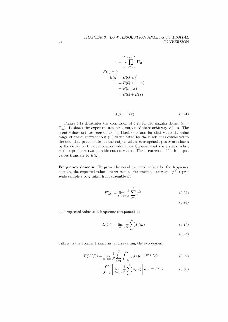
44CHAPTER 3. LOW RESOLUTION ANALOG TO DIGITAL
CONVERSION
v =
[?
m−1∏l=0
]Π∆
E(ε) = 0
E(y) = E(Q(w))
= E(Q(w + x))
= E(ε+ x)
= E(ε) + E(x)
E(y) = E(x) (3.24)
Figure 3.17 illustrates the conclusion of 3.24 for rectangular dither (v =Π∆). It shows the expected statistical output of three arbitrary values. Theinput values (x) are represented by black dots and for that value the valuerange of the quantizer input (w) is indicated by the black lines connected tothe dot. The probabilities of the output values corresponding to x are shownby the circles on the quantization value lines. Suppose that x is a static value,w then produces two possible output values. The occurrence of both outputvalues translate to E(y).
Frequency domain To prove the equal expected values for the frequencydomain, the expected values are written as the ensemble average. y(s) repre-sents sample s of y taken from ensemble S.
E(y) = limS→∞
1
S
S∑s=1
y(s) (3.25)
(3.26)
The expected value of a frequency component is:
E(Y ) = limS→∞
1
S
S∑s=1
F (ys) (3.27)
(3.28)
Filling in the Fourier transform, and rewriting the expression:
E(Y (f)) = limS→∞
1
S
S∑s=1
∫ ∞−∞
ys(τ)e−j·2π·f ·τdτ (3.29)
=
∫ ∞−∞
[limS→∞
1
S
S∑s=1
ys(τ)
]e−j·2π·f ·τdτ (3.30)
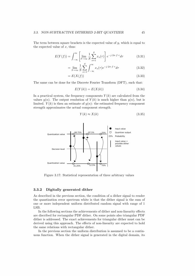
3.3. NON-SUBTRACTIVE DITHERED 2-BIT QUANTIZER 45
The term between square brackets is the expected value of y, which is equal tothe expected value of x, thus:
E(Y (f)) =
∫ ∞−∞
[limS→∞
1
S
S∑s=1
xs(τ)
]e−j·2π·f ·τdτ (3.31)
= limS→∞
1
S
S∑s=1
∫ ∞−∞
xs(τ)e−j·2π·f ·τdτ (3.32)
= E(X(f)) (3.33)
The same can be done for the Discrete Fourier Transform (DFT), such that:
E(Y (k)) = E(X(k)) (3.34)
In a practical system, the frequency components Y (k) are calculated from thevalues y(n). The output resolution of Y (k) is much higher than y(n), but islimited. Y (k) is then an estimate of y(n): the estimated frequency componentstrength approximates the actual component strength.
Y (k) ≈ X(k) (3.35)
Decision level
31.25%
68.75% 87.5%Quantization value
Quantization value
25%
Input value
Quantizer output
Probability
Input value + possible dither values
75%12.5%
25%
Figure 3.17: Statistical representation of three arbitrary values
3.3.2 Digitally generated dither
As described in the previous section, the condition of a dither signal to renderthe quantization error spectrum white is that the dither signal is the sum ofone or more independent uniform distributed random signal with range of 1LSB.
In the following sections the achievements of dither and non-linearity effectsare discribed for rectangular PDF dither. On some points also triangular PDFdither is addressed. The exact achievements for triangular dither must can bederived using this approach. The effects of non-linearity are expected to holdthe same relations with rectangular dither.
In the previous section the uniform distribution is assumed to be a contin-uous function. When the dither signal is generated in the digital domain, its

46CHAPTER 3. LOW RESOLUTION ANALOG TO DIGITAL
CONVERSION
distribution function is discrete: the signal can assume only a finite number ofvalues. Figure 3.18 shows the discrete and continuous PDF of a rectangulardither signal.
02d
p
0
M
2d
2 Mpa) b)
22
Continuous PDF
Discrete PDF
M2 M
Figure 3.18: Continuous and discrete rectangular PDF dither. a) eight discretedither values (M = 8), b) seven discrete dither values (M = 7).
AD
AD Dither
Generator
x y
Figure 3.19: Digitally dithered quantizer
The digital dither must be converted to the analog domain such that it canbe added to the analog signal before AD conversion. A basic digitally ditheredquantizer system is shown in Figure 3.19.
3.3.2.1 Achievements of digital dithering
When the dither signal is digital, the starting situation differs from the con-tinuous case discussed in section 3.3.1.3. The expected total error (ε) may beunequal to zero. Because the dither signal can only have a finite number ofvalues, so can the expected value of y.
Figure 3.20 illustrates how an input signal is converted to an expectedoutput value of the dithered quantizer. The granularity of the digital dither isvery low in this figure for clear illustration. The black dots represent arbitraryinput values, the horizontal bars connected to the dot represent the possiblevalues for w, given x. In this figure the range of the dither is 1 LSB, but dueto the low number of discrete values, the maximum value is clearly less than12 LSB. The cause of this difference is shown in Figure 3.18: the outer most
dither values are ∆2M spaced from the corresponding continuous PDF range. A
very important point is that the dither range is exactly 1 LSB. If this is notexactly the case, distortion is introduced.
When digital dither is applied there is a range for the input signal whichproduces the same value of E(y). In Figure 3.20 this is indicated by the grayareas. The possible values of E(y) is the combination of the possible dithervalues and the quantizer decision levels.
The fact that the input signal may vary, without a change of E(y) canbe translated to a totally different quantizer with the same number of outputvalues as possible values of E(y). For this totally different quantizer, the inputsignal may also vary in the same range, without a change of output signal.
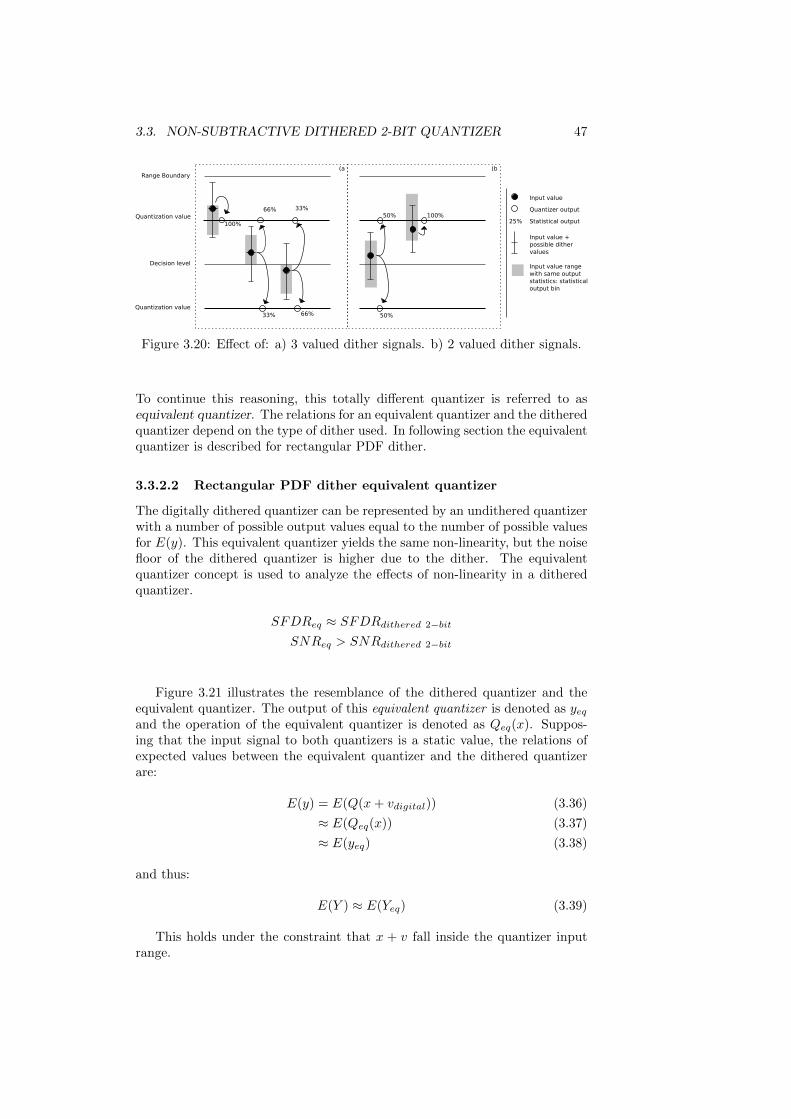
3.3. NON-SUBTRACTIVE DITHERED 2-BIT QUANTIZER 47
Decision level
33%
66%Quantization value
Quantization value
25%
Input value
Quantizer output
Statistical output
Input value + possible dither values
Input value range with same output statistics: statisticaloutput bin
100%
33%
66% 50%
50% 100%
Range Boundary(a (b
Figure 3.20: Effect of: a) 3 valued dither signals. b) 2 valued dither signals.
To continue this reasoning, this totally different quantizer is referred to asequivalent quantizer. The relations for an equivalent quantizer and the ditheredquantizer depend on the type of dither used. In following section the equivalentquantizer is described for rectangular PDF dither.
3.3.2.2 Rectangular PDF dither equivalent quantizer
The digitally dithered quantizer can be represented by an undithered quantizerwith a number of possible output values equal to the number of possible valuesfor E(y). This equivalent quantizer yields the same non-linearity, but the noisefloor of the dithered quantizer is higher due to the dither. The equivalentquantizer concept is used to analyze the effects of non-linearity in a ditheredquantizer.
SFDReq ≈ SFDRdithered 2−bit
SNReq > SNRdithered 2−bit
Figure 3.21 illustrates the resemblance of the dithered quantizer and theequivalent quantizer. The output of this equivalent quantizer is denoted as yeqand the operation of the equivalent quantizer is denoted as Qeq(x). Suppos-ing that the input signal to both quantizers is a static value, the relations ofexpected values between the equivalent quantizer and the dithered quantizerare:
E(y) = E(Q(x+ vdigital)) (3.36)
≈ E(Qeq(x)) (3.37)
≈ E(yeq) (3.38)
and thus:
E(Y ) ≈ E(Yeq) (3.39)
This holds under the constraint that x + v fall inside the quantizer inputrange.

48CHAPTER 3. LOW RESOLUTION ANALOG TO DIGITAL
CONVERSION
AD
AD Dither
Generator
AD
x
x y
y SFDR
SFDReq
FFT
FFT
Figure 3.21: Equivalent quantizer resulting in equal distortion component mag-nitude
Rectangular PDF dither When the dither signal can assume M values,vd is the PDF of the dither signal:
vd(x) =
M−1∑c=0
1
Mδ
(x− (
−∆
2+
∆
2 ·M+c ·∆M
)
)(3.40)
and dD−bit is the set of decision levels for a D-bit quantizer:
dD−bit(x) =
2D−1∑d=0
(1
2D − 1δ
(x− 2D − 1
2·∆ + d ·∆
))(3.41)
The set of possible values for E(y) is separated by a set of equivalent quantizerdecision levels which are defined as the convolution of vd and d2−bit:
dE(y) = vd ∗ d2−bit (3.42)
So while y can only assume 2D values, the number of expected values of y isincreased by the digital dither. This effect is illustrated in Figure 3.22. Forthis type of dither, the maximum input signal range is equal to the rangeof the convolution result. As will become clear, for other dither signals, theconvolution result will contain values which are out of the allowed input signalrange and therefore not used. For a D-bit quantizer and a rectangular PDFdither signal with M discrete values, the number of quantizer decision levelsare:
(2D − 1) ·M (3.43)
and the number of possible values of E(y) is:
(2D − 1) ·M + 1 (3.44)
The use of the concept of the equivalent quantizer is illustrated by simula-tion for rectangular PDF dither. A spectrum plot of a dithered quantizer andits equivalent undithered quantizer is shown in Figure B.3.

3.3. NON-SUBTRACTIVE DITHERED 2-BIT QUANTIZER 49probability
2 20* = vd
d2-bit
E(y)d
Figure 3.22: Convolution of rectangular dither PDF and quantizer decisionlevels result in decision level distribution.
0 0.1 0.2 0.3−60
−50
−40
−30
−20
−10
0
Relative frequency [f/fs]
Mag
nitu
de [d
BF
s]
log2(25)−bits quantized sine wave spectrumSFDR: 35.4025 [dB]
0 0.1 0.2 0.3−60
−50
−40
−30
−20
−10
0
Relative frequency [f/fs]
Mag
nitu
de [d
BF
s]
2−bits quantized sine wavewith 3−bit dither spectrum
SFDR: 35.7838 [dB]
Figure 3.23: Spectra of a log(25)-bits equivalent quantizer and the 3-bit rect-angular dithered 2-bit quantizer: they have approximately the same SFDR.(MATLAB code in appendix C.3)
Triangular PDF dither. For triangular dither a similar relations exist.These are worked out to certain extend and are listed in appendix B.4, butdue to time limitations correctness cannot be guaranteed. Simulation showthat the equivalent quantizer SFDR approximates the SFDR of the ditheredquantizer.
Theoretical SFDR The theoretically achievable SFDR of a rectangulardithered quantizer can be expressed by modifying 3.2. The resolution of theequivalent quantizer is the log2 of the number of quantization values (Equation3.44):
(2D − 1) ·M + 1
The SFDR of a dithered D-bit quantizer, with M different dither valueshas a maximum value of:
SFDR ≈ 8.07 · log2((2D − 1) ·M + 1)) + 3.29 (3.45)
3.3.3 Non-linearity
Until now the non-linear behavior of a (dithered) quantizer is discussed whenall components are assumed ideal. In practice other non-linearities will alsobe present. The dithered quantizer consists of a dither DAC and a quantizer.

50CHAPTER 3. LOW RESOLUTION ANALOG TO DIGITAL
CONVERSION
The effect of non-linearity for both sub-systems are discussed in this section.Because of the variable decision levels of the targeted ADC concept, the non-linearity of the quantizer is discussed in more detail. The non-linearity effectsare analyzed by looking using the equivalent quantizer concept. The analy-sis is done for rectangular dither, because of time constraints. The relationsidentified in next sections are not directly applicible to triangular dither.
Errors of the output values of the dither DAC and errors of the decisionvalues of the 2-bit quantizer can be translated to multiple errors in the decisionvalues of the equivalent quantizer. When rectangular PDF dither is used, inthe ideal case, each equivalent quantizer decision level is determined by a single2-bit quantizer decision level and a single dither DAC output value. Althoughin this section the low-resolution quantizer is assumed to be 2-bit quantizer,the line of reasoning is valid for quantizers with a other resolutions as well.
3.3.3.1 Dither DAC non-linearity
The dither DAC error results in errors for multiple decision levels of the equiva-lent quantizer. Equation 3.42 shows that the dither range affects the equivalentquantizer output for each 2-bit quantizer decision level. For example, when onepossible dither DAC output value is higher than intended, the equivalent quan-tizer has 3 decision levels which are higher than expected.So the non-linearityof the dither DAC has a repetitive effect on the non-linearity of the ditheredquantizer. Figure 3.24 illustrates this repetitiveness for a 2-bit quantizer anda 3-bit digital dither signal. It shows the Integral Non-Linearity (INL) of theequivalent quantizer (and thus also the possible expected output values of thedithered quantizer).
INL
Output
INL
Output
a)
b)
Figure 3.24: Repetitive INL due to INL of dither DAC and quantizer. a) INLof the dither DAC. b) INL of equivalent quantizer.
3.3.3.2 Quantizer non-linearity
When a 2-bit quantizer decision level deviates from its intended value, thisresults in multiple decision levels of the equivalent quantizer to deviate fromtheir intended values. For the dithered quantizer this means that all expectedvalues of the output depending on the deviating 2-bit quantizer decision leveldeviate by the same amount, this can be concluded from Equation 3.42.
Figure 3.25 illustrates the INL for a 2-bit quantizer and a 3-bit digital dithersignal where the lower decision level has a higher value than intended.
Any change in the decision levels can always be translated to an increaseof the lower decision level value and scaling of the signal for a 2-bit quantizer.Therefore only the case of an increase of lower decision level value is considered.

3.3. NON-SUBTRACTIVE DITHERED 2-BIT QUANTIZER 51
INL
Output
INL
Output
a)
c)
b)
INL
Output
Figure 3.25: Repetitive INL due to INL of dither DAC. a) INL of the ditherDAC. b) INL of the 2-bit quantizer. c) Statistical INL of the dithered quantizer.
The effects of this error are analyzed in next paragraphs by looking at the effectson the equivalent quantizer.
Equivalent quantizer with decision level error. An error in decisionlevels add distortion to the quantized signal. In order to calculate the addeddistortion caused by an error in the lower decision level, the concept of theequivalent quantizer is used. The function of the equivalent quantizer is denotedas EQ(). A decision level error of the 2-bit quantizer (Q) changes the rangesfor which the input value has the same output value: the quantizer transferfunction is changed. The change in the equivalent quantizer input signal rangesis illustrated in Figure 3.26. The gray areas represent ranges of the input signalwhich produce equal output values. In this figure the output values defined bythe lower decision level of the 2-bit quantizer are shifted by the same amount asthis decision level is changed. Thus when a sine wave is input to the equivalentquantizer (EQ), the output signal is distorted because of the changed quantizerfunction.
Decision level
Range boundary
Decision level
Decision level
Range boundary
2-bit quantized signal No decision level error Decision level error
Figure 3.26: Decision level error effect on input signal ranges (gray areas),which lead to an output value
To analyze the effect of non-linearity, the ideal equivalent quantizer is com-pared to the equivalent quantizer with an error (caused by the error in the 2-bitquantizer decision level). To distinguish between the ideal equivalent quantizerand the one with the error, the following transfer functions are defined:
• EQ: the ideal quantization function of the equivalent quantizer.
• EQe: the equivalent quantizer adjusted for the decision level error.

52CHAPTER 3. LOW RESOLUTION ANALOG TO DIGITAL
CONVERSION
SFDR degradation In this paragraph an expression is presented, by whichthe SFDR can be found of the 2-bit dithered quantizer with an error in adecision level.
The SFDR of EQe can be calculated by applying a sine wave to the inputand Fourier transforming the output signal. A nice description of the outputsignal depending on the decision level error is not easy to find. A description forfrequency components of a sine wave quantized by EQ is available in literature[18]. To find a nice expression for the SFDR of the equivalent quantizer, theequivalent quantizer non-linearity error signal is defined:
• eEQ(x) = EQ(x)− EQe(x): The equivalent quantizer error due to deci-sion level error.
The error signal value as a function of an input sine wave is given in Equa-tion 3.46. The derivation is given in Appendix B.3.1. This expression allowsto calculate the added distortion due to a decision level eror.
eEQ(sin(2π · t)) =
1 if [b(c,M)] > sin(2π · t) > [b(c,M) + (1− α)∆] ,
∀c ∈ {M2 ,M2 + 1, ...( 3·M
2 − 1)}0, otherwise
(3.46)
In this expression b(c,M) is decision level c and (1 − α)∆ is the shift of thisdecision level due to the error in the 2-bit quantizer decision level.
b(c,M) = −[
∆ · c2M
· 4∆
A∆
](3.47)
Where 2M is the number of dither values, α is the decision level error in LSBand A∆ is the amplitude of the input sine wave in LSBs. For rectangular ditherthis is 3
2 . Figure 3.27 shows how eEQ(sin(2π · t)) relates to sin(2π · t).The frequency components of the sine wave quantized by EQ are expressed
by Blachman’s approach [19] and the frequency components of the error eEQpresented. When this is summed, the total spectrum is obtained and the SFDRis calculated.
The magnitude of frequency components of EQ(sin(2π · t)) [18]:
EQ(p) = ∆
(A∆ · δ(p− 1) + 2 ·
∞∑n=1
(−1)n
πnJp(2π · n ·A∆)
)(3.48)
For p is positive and odd. The magnitude of frequency components of eEQ(sin(2π·t)) are calculated by applying the Fourier transform to eEQ(sin(2π · t)):
F (eEQ(sin(2π · t)))(p) =
M∑c=1
[∫ π+A(c,M)
π+B(c,M)
∆ · e−i·p·tdt
]+
M∑c=1
[∫ 2π−B(c,M)
2π−A(c,M)
∆ · e−i·p·tdt
] (3.49)
Where the integration borders are b(c,M) scaled by the sine wave amplitudeand input to the arcsin function:
A(c,M) = sin−1 (b(c,M)) (3.50)
B(c,M) = sin−1 (b(c,M) + (1− α)∆) (3.51)
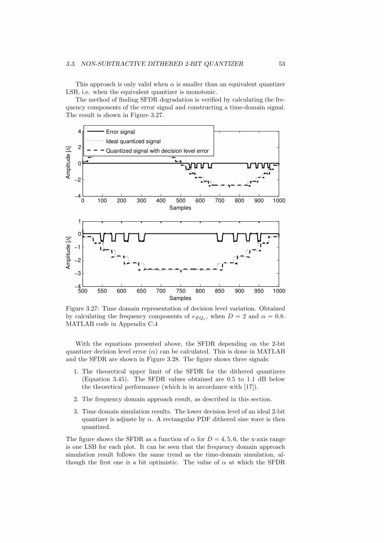
3.3. NON-SUBTRACTIVE DITHERED 2-BIT QUANTIZER 53
This approach is only valid when α is smaller than an equivalent quantizerLSB, i.e. when the equivalent quantizer is monotonic.
The method of finding SFDR degradation is verified by calculating the fre-quency components of the error signal and constructing a time-domain signal.The result is shown in Figure 3.27.
0 100 200 300 400 500 600 700 800 900 1000−4
−2
0
2
4
Samples
Amplitude
[�]
500 550 600 650 700 750 800 850 900 950 1000−4
−3
−2
−1
0
1
Samples
Amplitude
[�]
Error signal
Ideal quantized signal
Quantized signal with decision level error
Figure 3.27: Time domain representation of decision level variation. Obtainedby calculating the frequency components of eEQe , when D = 2 and α = 0.8.MATLAB code in Appendix C.4
With the equations presented above, the SFDR depending on the 2-bitquantizer decision level error (α) can be calculated. This is done in MATLABand the SFDR are shown in Figure 3.28. The figure shows three signals:
1. The theoretical upper limit of the SFDR for the dithered quantizers(Equation 3.45). The SFDR values obtained are 0.5 to 1.1 dB belowthe theoretical performance (which is in accordance with [17]).
2. The frequency domain approach result, as described in this section.
3. Time domain simulation results. The lower decision level of an ideal 2-bitquantizer is adjuste by α. A rectangular PDF dithered sine wave is thenquantized.
The figure shows the SFDR as a function of α for D = 4, 5, 6, the x-axis rangeis one LSB for each plot. It can be seen that the frequency domain approachsimulation result follows the same trend as the time-domain simulation, al-though the first one is a bit optimistic. The value of α at which the SFDR

54CHAPTER 3. LOW RESOLUTION ANALOG TO DIGITAL
CONVERSION
starts decreasing is roughly equal. The error of α becomes noticeable when theerror is bigger than 1
3 an LSB of the equivalent quantizer.From these results a certain allowed decision level deviation is found. For
instance, when the targeted SFDR is 60 dB for instance, a dither resolutionof 6 bits is required and that the the decision level error error may not exceedhalf a dither signal LSB.
0.95 1
40
42
44
46
48
�
SFD
R[d
B]
Dither resolution: 4 bits
0.98 142
44
46
48
50
52
54
56
�
SFD
R[d
B]
Dither resolution: 5 bits
0.99 0.995 1
54
56
58
60
62
64
�
SFD
R[d
B]
Dither resolution: 6 bits
Time domain SFDR
Frequency domain SFDR8.07 log ((2 -1) M +1) + 3.29D
2
Figure 3.28: SFDR as a function of α. The x-axis range is 1 LSB.
3.3.4 Random number generators
A dither signal is a signal with random values. True random values are non-deterministic, which is difficult to generate by a digital system because oper-ations of a digital system tend to be deterministic. A pseudo-random numbergenerator can be used for dithering purposes. The output of this generatoris deterministic, but its statistical properties can be sufficient to be used as arandom number generator. The output will cycle through all its possible valuesin a pseudo-random order.
Many pseudo random generators consists of a Linear Feedback Shift Regis-ter (LFSR). A LFSR generates linear recursive sequences: they cycle through2n − 1 output values, where n is the number of registers used for the LFSR.The two most well known types of LFSR are the Fibonacci and Galois gener-ator [27], both types are shown in Figure 3.29. In this figure the states of theswitches are denoted by gm.
The Galois generator can operate faster, because it has less logic gates inthe feedback loop. The generators will output all possible values if the valuesfor gm are chosen properly [28].

3.4. SUMMARY AND CONCLUSIONS 55
gm gm-1 gm-2 g2 g1 g0
gmgm-1gm-2g2g1g0
a)
b)
Figure 3.29: Linear shift feedback registers. a) the Fibonacci generator. b) theGalois generator
3.4 Summary and conclusions
Summary Analog to digital conversion involves sampling and quantization.Quantization is a non-linear operation and introduces distortion. The magni-tude of the distortion components in the spectrum depend on quantizer reso-lution. Adding dither to the input signal of a quantizer reduces the distortioncomponents.
Non-subtractive dithering increases the noise floor in the measured spec-trum, but does not consume bandwidth as with band-limited dither or increasedigital complexity as with subtractive dither. A mathematical approach is in-troduced which allows the derivation of the expected performance of a 2-bitdithered quantizer. For dithering with a signal with a rectangular or triangu-lar PDF, the total error of the dithered quantizer has a white spectrum whichallows highest SFDR. The concept of the equivalent quantizer is introduced,which gives insight in the achievable performance of a dithered quantizer. Alsothe the effects of non-linearity of the quantizer can be investigated using theequivalent quantizer concept.
Non-linearity introduced by error in the quantizer decision levels leads todegradation in SFDR. An approach to find the SFDR based on the equivalentquantizer concept, for a decision level error, is presented. A maximum alloweddeviation of the decision level for a certain SFDR is found. In this analysis, theeffects of rectangular PDF dither are examined. Rectangular dither results ina varying noise floor and thus some noise uncertainty. However, the noise flooris lower than when triangular dither is applied and rectangular dither allowslarger input signal swing. Generation of digital dither can be done by using alinear feedback shift register, which produces a pseudo-random digital signal.
Conclusions Different dithering schemes are discussed and one is most suit-able for an energy detection spectrum analyzer: non-subtractive wide-banddithering with rectangular or triangular dither PDF. This dithering schemeallows low-resolution digital processing and does not consume measurementbandwidth, but it raises the noise floor.
Triangular dither results in a higher noise floor in the measured spectrumthan rectangular dither. However, rectangular dither results in a dependencybetween signal and added noise power. When the mean and power of the inputsignal is controlled, the variation of noise floor power is limited to a small range.

56CHAPTER 3. LOW RESOLUTION ANALOG TO DIGITAL
CONVERSION
Whether this noise uncertainty dominates the achievable system performancedepends on the total system it is used in. The noise uncertainty introduced byrectangular dithering is assumed to be acceptable for this thesis. The equivalentquantizer concept is an effective tool to analyze the performance of a digitallydithered quantizer.

Chapter 4
System level design
Chapter 2 described the cross-correlation spectrum analyzer and how it in-creases the SFDR compared to traditional spectrum analyzers. Then Chapter3 described sampling and quantization and zoomed in to a 2-bit quantizer anddescribed dithering as a countermeasure for distortion.
The goal of this chapter is to introduce the revisited ADC concept, originat-ing from ASTRON, and to investigate the suitability for the use in a cognitiveradio energy detection spectrum analyzer. The performance dependency of thespectrum analyzer on ADC characteristics are investigated.
This chapter describes the system level design and simulation results of adigitally dithered 2-bit ADC with automatic gain control and offset cancelingfor the use in this cross-correlation spectrum analyzer. Uncorrelated ditheris added in both signal paths and the dither and quantization noise floor islowered by utilizing the cross-correlation spectrum analyzer. Thereby a higherSFDR is achieved than for a traditional spectrum analyzer with a dithered2-bit ADC.
In the following sections, first system level choices and calculations arepresented. Based on the expected performance of the ADC, a SFDR of 60 dBis expected to be achieved after cross-correlation, for a resolution bandwidth of6 MHz . The ADC concept is introduced, then an abstract view on the loop ispresented and an implementable block diagram is presented. Specifications andsettings are derived for the ADC sub-blocks. The ADC concept is implementedin SIMULINK, the simulation results are shown and discussed. Also someexpectation for a CDF-based AGC ADC with a higher resolution are discussed.
4.1 Cognitive radio standard
The ADC concept described in this chapter is designed for the use in a cog-nitive radio system. In this section relevant numbers from one cognitive radiostandard are presented.
FCC, Ofcom and IEEE are working on standards for cognitive radio. Thestandards differ a little and therefore the IEEE 802.22 standard is used for sys-tem calculations. Depending on geographic location, the DTV band is dividedinto channels with three different widths [29].
1. DTV band: 54MHz− 862MHz
57

58 CHAPTER 4. SYSTEM LEVEL DESIGN
2. Channel width: 6, 7 or 8 MHz.
3. Sensitivity limit: −116dBm in a 6MHz wide channel
4. Back-off time: 2s: When the used channel becomes occupied, the systemhas this time to switch to another channel.
Solutions proposed in literature, where the goal is to meet the sensitivitylimit requirement of −116dBm/6MHz often use knowledge on the signal, suchas pilot tones or other cyclostationary properties [30]. The spectrum analyzer ofthis thesis is designed as being a part of a cognitive radio system where possiblyalso other spectrum sensing techniques are applied. In this case, the energydetection spectrum analyzer gives a first coarse estimation of the spectrum.Then a more advanced spectrum sensing mechanism determines if one of thepotential channels are free.
4.2 Spectrum analyzer front-end
The cross-correlation spectrum analyzer consists of an analog front-end and adigital back-end, separated by the ADCs. In order to derive specifications andrequirements of the ADC, the characteristics of the analog front-end must bedefined. First two concepts for the analog front-end are discussed
4.2.1 Analog front-end concepts
In many analog front-ends, the signal picked up by the antenna is mixed downto the IF band. This is done because the bandwidth of the signal of interestlies beyond the bandwidth of the ADC and digital back-end, or because suchthe bandwidth leads to large power consumption.
In previous work [4], the cross-correlation spectrum analyzer consists of aquadrature mixer concept. The advantage of quadrature mixing is that nega-tive frequencies can be distinguished from positive frequencies, because of thecomplex input signal representation.
The frequency range of the DTV band is relatively low: it starts at 54 MHzand stops at 862 MHz. When quadrature mixing is used, the sample frequencyis reduced but at the cost of another mixer, anti alias filter and ADC.
Choosing for a zero-IF quadrature mixer concept instead of a mixer-lessconcept is justified when the power consumption reduction outweighs the costof additional hardware, for equal performance. Because in previous work azero-IF mixer concept is used and because a mixer-less concept might be agood solution, both cases are addressed in this section.
4.2.2 Expression of signal power
The input signal power received at the antenna is expressed in Watt. Whenthe signal is amplified using automatic gain control, the ratio between analoginput signal power and output signal power is variable. Therefore, the outputsignal power is expressed in a different unit than the input signal power. Theinput signal is often expressed relative to one milliwatt. The output signal willbe expressed in decibels relative to a full scale (complex) sine wave (dBFs).
4.3. THEORETICAL SYSTEM PERFORMANCE 59
The output signal is referred to a complex sine wave or a non-complex sinewave, depending on the system discussed.
Power expressed relative to a full scale sine wave When a full scalereal signal is expressed in dBFs, the amplitude is half full scale and its poweris:
P =
(FS2
)22
(4.1)
=1
8· FS2 (4.2)
where FS denotes full scale. The power of a full scale sine wave is then:
10 · log10
18 · FS
2
18 · FS2
= 0[dBFs] (4.3)
Relative to a full scale complex sine wave When a full scale complexsine wave is converted to the digital domain, both its real and imaginary partsare converted by separate ADCs. The amplitude of the real and imaginary partare then half the input range of the ADC. The power of a full scale complexsinusoid is thus:
Preal + Pimaginary =
(FS2
)22
+
(FS2
)22
(4.4)
=1
4· FS2 (4.5)
The power in decibels of a full scale complex sine wave is then:
10cdot log10
14 · FS
2
14 · FS2
= 0[dBFs] (4.6)
4.3 Theoretical system performance
This section presents the system calculations for the two front-ends in mind.
4.3.1 Choices and calculations
First the choices are presented on which the theoretical performance calcula-tions are based.
Choices
1. Maximum frequency.
• In case of zero-IF mixer concept: If the spectrum analyzer consist ofa quadrature mixing zero-IF front-end (in accordance with previouswork), then the DTV band is down-mixed to around 0HZ, Forinstance with an oscillator frequency of 460MHz. The maximumfrequency is then approximately 405MHz.

60 CHAPTER 4. SYSTEM LEVEL DESIGN
• In case of mixer-less concept: The maximum frequency is definedby the cognitive radio standard: 862MHz
2. Sample frequency and resolution bandwidth: The channel bandwidths forDTV vary per country and the channels are not uniformly distributedover the DTV band. However, for the validation of the ADC concept,the resolution bandwidth is chosen to be 6 MHz.
When the signal is down-mixed to around 0 Hz, the IF bandwidth rangesfrom − 862−54
2 to 862−542 . The minimal sample frequency is:
862− 54 = 808MHz (4.7)
Because the anti-aliasing filter requires some bandwidth, the sample fre-quency is chosen higher. The sample frequency is chosen based on theresolution bandwidth of 6MHz and taking into account convenient FFTimplementation (i.e. the number of channels is a power of two). Thesample frequency for a zero-IF mixer concept is then:
fs = 1536MHz (4.8)
When the mixer-less concept is used, the frequency is doubled:
fs = 2 · 1536 = 3072MHz (4.9)
The number of channels in one spectrum is then:
#channels = 2dlog2( 862−546 )e = 256 (4.10)
3. Analog front-end gain The zero-IF front-end used in previous work [4]consists of a passive splitter to divide the signal power over the twoparallel front-ends. In [5] a variable attenuator is described as part of across-correlation spectrum analyzer. The front-end in mind, for which theCDF-based AGC ADC is worked out, consists of this variable attenuator.The attenuation is tunable in steps of 6 dB.
4. ADC concept: The analog to digital conversion is done by a dithered2-bit CDF-based AGC ADC. This is the revisited ADC concept fromASTRON. It includes automatic gain control and offset canceling. Theoffset canceling suits the zero-if mixer concept, because this concept in-troduces offset when input signal frequency components are close to themixer local oscillator frequency. The input signal is properly scaled bythe automatic gain control. The ADC uses dithering to remove distortioncomponents when strong narrow-band signals are input to the spectrumanalyzer.
5. Dither signal: The dither added to both parallel input signals are statisti-cally independent complex valued signals with a rectangular or triangularPDF. The noise floor is now raised by quantization noise and dither noise.Uncorrelated dither signals are added to both signal paths such that thequantization and dither noise floor is lowered by cross-correlation.

4.3. THEORETICAL SYSTEM PERFORMANCE 61
6. SFDR determination: The theoretical SFDR is based on a zero meansine wave with amplitude 3
4 (rectangular PDF dither) and 12 (triangu-
lar PDF dither) of the input range of the quantizer, depending on thetype of dither used. For the calculation no other noise than dither andquantization noise is present.
system calculations
1. Noise and distortion (in case of no dither): For a 2-bit ADC the powerof the quantization noise power, when assumed white, is:
q(w)2white =
∆2
12(4.11)
The resulting noise floor is then:
NoiseF loorq = 10 · log10(∆2
12)− 10 · log10(#channels) (4.12)
The worst case SFDR of a 2-bit quantizer is, according to equation 3.2:
SFDRwc = 8.07 · 2 + 3.29 = 19.43[dB] (4.13)
2. Noise and Distortion (in case of dither) Rectangular dither and triangu-lar dither power respectively:
v2r =
∆2
12(4.14)
v2t =
∆2
6(4.15)
When added to the input signal of the quantizer, the noise floor is dom-inated by the quantization noise power and dither power (total errorpower, see 3.2). For the rectangular PDF, dither this depends on theinput signal. Although this is subject to recommended further research,the total error power is approximately ∆
12 + ∆12 when the input signal is
properly scaled, thus:
NoiseF loorεr = 10 · log10(∆2
12+
∆2
12)− 10 · log10(#channels) (4.16)
NoiseF loorεt = 10 · log10(∆2
12+
∆2
6)− 10 · log10(#channels) (4.17)
3. SFDR (in case of dither): For rectangular PDF dither, the input sinewave is scaled by 3
4 and for the triangular PDF dither it is scaled by 12 .
When proper dithering is applied, the distortion components are reduced

62 CHAPTER 4. SYSTEM LEVEL DESIGN
to below the noise floor. The SFDR in both cases then is:
SFDRr = 20 · log10(3
4)−NoiseF loorεr (4.18)
= 20 · log10(3
4)− 10 · log10(
∆2
12+
∆2
12)− 10 · log10(#channels)
(4.19)
SFDRt = 20 · log10(1
2)−NoiseF loorεt (4.20)
= 20 · log10(1
2)− 10 · log10(
∆2
12+
∆2
6)− 10 · log10(#channels)
(4.21)
4. Cross-correlation Thus the increase in SFDR due to cross correlation is(equation 2.9):
I = 10 · log10(√Tm ·RBW ) (4.22)
(4.23)
5. SFDR (in case of dither and cross-correlation) Which gives a theoreticalachievable SFDR for rectangular PDF dither and triangular PDF ditherof:
SFDRr = 20 · log10(3
4)− 10 · log10(
∆2
12+
∆2
12)− 10 · log10(#channels)
+10 · log10(√Tm ·RBW )
(4.24)
(4.25)
SFDRt = 20 · log10(1
2)− 10 · log10(
∆2
12+
∆2
6)− 10 · log10(#channels)
+10 · log10(√Tm ·RBW )
(4.26)
Table 4.6 shows the achievable SFDR values based on the calculations pre-sented above, for a measurement time of 0.2 seconds. In general: the smallerthe Resolution Bandwidth (RBW), the higher the SFDR, but the measurementof a spectrum takes more time and thus the cross-correlation effect is smaller.Based on these numbers, the ADC concept is worked out for a resolution band-width of 6 MHz. A margin for the SFDR is used for the noise uncertainty dueto limited measurement time: the targeted SFDR for the ADC concept is 60dB when rectangular dither is used.
The utilization of the cross-correlation allows a significant increase in SFDRfor a 2-bit ADC.
4.4 The ADC concept
The ADC concept originates from ASTRON [8], where it was implementedwith discrete components. In this section the concept is revisited and designedfor on-chip integration. The ADC is referred to as CDF-based AGC ADC.

4.4. THE ADC CONCEPT 63
RBW Number SFDR, no XC [dB] SFDR, XC [dB] XC Gainof channels (Rect,Triang) (Rect,Triang) [dB]
200 kHz 7680 47.1, 41.9 69.6, 64.3 236 MHz 256 32.4, 27.1 62.7, 57.4 30.47 MHz 220 31.7, 26.4 62.33, 57.0 30.78 MHz 192 31.1, 25.8 62.0, 56.8 31
Table 4.1: Achievable SFDRs for different resolution bandwidths
4.4.1 The use in radio astronomy
In radio astronomy knowledge on the input signal to the ADC is available, asopposed to cognitive radio. In radio astronomy the input signal is Gaussiandistributed and white over the entire measured band. In cognitive radio theinput signal can be Gaussian distributed with a bandwidth which is a fractionof the measured band. This is the reason that dithering is not required in theseradio astronomy applications. The input signal provides the dithering effectitself: the quantization noise is white because the input signal is white. Notonly is the quantization noise white, but also clipping distortion is white.
This difference in input signals is the reason why the ADC concept for cog-nitive radio yields different results than for radio astronomy. System settingsderived in the decision probability rules section (Section 4.4.6) are differentthan system settings in [8], [7].
4.4.2 Introduction to the ADC concept
The CDF-based AGC ADC is a 2-bit ADC with automatic gain control andoffset canceling. When a signal is digitized, the amplitude ratio between theanalog and digital signal is determined by the ADC. To achieve variable gainthere are two possibilities. The first is amplifying the input signal by a variablegain block prior to AD conversion. The second is adjusting the full-scale rangeof the ADC. The CDF-based AGC ADC is based on a flash ADC and has avariable full-scale range. The full-scale range is adjusted based on estimationsof the CDF of the input signal. A CDF of a signal is a function (CDF (x)) thatwill give the probability that the signal is less than or equal to x. The CDFof a signal thus also provides information on its amplitude. When the CDF isestimated, this amplitude information is estimated and the full-scale range ofthe ADC is adjusted accordingly.
The expected input signal to a cognitive radio system is a strong narrow-band signal (e.g. FM signals), a combination of a few strong narrow-bandsignals (e.g. Multiple FM signals) or Gaussian distributed signals (e.g. OFDMsignals). The CDF of sinusoidal or Gaussian distributed signals are known.For signals with known CDFs, the relation between decision level probabilityand amount of clipped distortion is known. Clipping distortion is present wheninput signal samples fall outside the ADC input range. Because instantaneousvalues of a Gaussian distributed signal can have any value theoretically, thereis always some clipping distortion. The ADC must make sure that the amountof clipping distortion is small enough such that it does not degrade the targetedSFDR. Thus the decision levels of the ADC are set such that maximal SFDR

64 CHAPTER 4. SYSTEM LEVEL DESIGN
is achieved.A signal consisting of multiple sinusoids can have many different CDFs
because of phase differences between the sinusoids. The CDF then must bepredicted or estimated, such that the amount of distortion is limited to accept-able levels. This issue will be elaborated in section 4.4.6.
LUTout
in2
1
1
1
dpd0dn
Cum
ula
tivepro
bability
n
Signal value
1
0
Controller
p0
Figure 4.1: Flash ADC with decision levels set through the input signal CDF.
Figure 4.1 shows the concept of the ADC. Three comparators convert theanalog signal to a digital signal, like a flash ADC. The reference level of eachADC is determined through the input signal CDF. The probabilities are deter-mined by a digital subsystem, referred to as the system-controller. Each deci-sion level corresponds to a certain probability that the input signal is higherthan that decision level, as shown in Equation 4.27. This equation reveals akind of loop, as dout is proportional to a function of din and dout determinesdin.
dout ∝ px(x > din) (4.27)
Assumptions The ADC acts on estimations of the CDF of the input signal.A starting point of the energy detection spectrum analyzer for cognitive radio isthat it has no information on the input signal. However to say something aboutthe expected behavior of any ADC, some assumptions have to be made. For thesystem level design of the CDF based AGC ADC, the following assumptionsare made:
1. The PDF of the input signal is symmetric around the mean of the signal.This is a necessary condition to have uniform quantization.
2. The input signal statistics are constant during the measurement of onespectrum. When this is not the case, the estimated spectrum is ambigu-ous because signals with different statistics are averaged.

4.4. THE ADC CONCEPT 65
During system design it turned out that the first assumption is not valid forcertain signals. This problem is addressed in section 4.4.8.
Automatic gain control and offset canceling The desired decision levelprobabilities are predefined by the system. The decision level values thenresult via the CDF of the input signal. The three decision levels are denotedas [dn, d0, dp]. When the input signal has less pwoer, the range of its CDF issmaller and the decision levels are changed accordingly. Also when an offsetis added to the signal, its CDF changes and so do the decision levels. This isillustrated in Figure 4.2.
Cumulativ
eprobability
n 0 p
Signal value
1
0
decision levels
Figure 4.2: Reference levels are adapted to CDF changes: a positive offset isintroduced and the amplitude is decreased.
From CDF estimate to decision level loop For three decision levels,three points in the CDF are estimated. Each probability can be estimated bycounting the number of input values that are higher than the correspondingdecision levels in a certain interval. Another representation of the probabilitiesis obtained when this counter signal is low pass filtered.
The result of the low pass filtered counter signal is compared to a referenceset by the controller. The decision level is then adapted accordingly. Whenthe results of the quantization are then fed-back to the decision level a decisionlevel loop is created.
4.4.3 Power estimation
To give any meaning to the resulting spectrum, a power reference is needed.The value of an LSB is equal to the distance between two adjacent decisionlevels, so each ADC defines an LSB in twofold. In the proposed implementationin the following sections the value of an LSB is available in the digital domain.Figure 4.3 illustrates the two LSBs known to the system. The two definitionsof an LSB are expected to be equal and their average is used as the powerreference. The spectrum analyzer consists of multiple ADCs (two for direct-conversion and four for quadrature-conversion), so there are multiple powerreferences available, which can again be averaged.

66 CHAPTER 4. SYSTEM LEVEL DESIGN
Range boundary
Decision level
Quantization value
LSBs knownsystem
Figure 4.3: Quantizer LSBs known to system
4.4.4 Decision level loop
As became clear from Equation 4.27, each decision level is determined by afeedback loop. A single ADC consists of three decision levels and thus threedecision level loops. Each loop sets that decision level independently. Theinput signal and the desired decision level probability are inputs to this loop.In the following sections, first an abstract view is presented on the decisionlevel loop and then an implementable block diagram of the loop is presented.
4.4.4.1 Abstract view
When looking at the decision level loop by looking at Equation 4.27 and Figure4.2, only two signal expressions are of interest: decision level values(d) and em-phthe probability of a signal being less then or equal to d (px(x > d)) . Thoseunits are related to the CDF of the input signal, so in the abstract view onlythose units are considered. Figure 4.4 shows the abstract decision level loop.
A decision level loop has three tasks:
1. Compare the input to the decision level.
2. Estimate the probability that the input signal is higher than the decisionlevel: estimate px(x > d) .
3. Adapt the decision level value.
The comparison results in an estimation of the probability that the inputsignal is larger than the decision level. This probability is denoted as pd. prefis the reference probability (which is the desired probability for pd) and is setby the system controller. The difference between these two probabilities is theerror probability ∆p, and must converge to zero. To let the error converge tozero, ∆p is integrated before it is converted to a decision level. The integrationalso filters out the high frequencies of ∆p, which bears relevance when theimplementation is concerned.
4.4.4.2 Decision level loop blocks
The abstract blocks of Figure 4.4 are filled in with realistic functions, such thatan implementable version of the decision level loop emerges. This decision levelloop is shown in Figure 4.5. The following choices are made:
1. The signal (w(t)) entering a decision level loop is a voltage, so the decisionlevel (d(t)) is also a voltage.

4.4. THE ADC CONCEPT 67
pref
p
CDFx
pd
pref
pd(t)
d(t)
pd
d
p
w(t)y(t)
p
Figure 4.4: Abstract representation of CDF-based decision level loop. (Thecompare function is in this abstract representation not a comparator.) The in-put signal is compared to d(t), which results in a probability pd, this probabilitydiffers from the reference probability pref . The difference is integrated (
∫∆p)
and converted to a decision level (d(t)). Because the difference is integrated,pd converges to pref , as is indicated by the small CDF plots.
2. The comparison block is a clocked comparator, the clock frequency equalsthe sample frequency of the total ADC. The output of this comparator(pd(t)) is combined with other comparator outputs and results in thedigital output signal of the total ADC.
3. The output of the comparator (pd(t)) is low-pass filtered which results ina higher-resolution digital signal (pd(t)).
4. The difference between (pd(t)) and the reference probability (pref ) is theprobability error (∆p) and is obtained by subtracting those digital signals.The result is integrated by a digital integrator. The digital integrator isfollowed by a gain block to control the dynamics of the loop.
5. The decision level is converted from the digital domain to the analogdomain by a DAC.
Figure 4.5 shows the implementable decision level loop block diagram.The resolution of (pd(t)), pref and ∆p and the DAC are derived when the
total ADC is addressed (Section 4.4.5).
4.4.4.3 Frequency behavior
The low-pass filter and integrator limit the bandwidth of the decision level.Because the filter and integrator are part of the feedback, the loop itself isa high-pass filter. Figure 4.6 shows the effect of the decision level loop inthe frequency domain: the low-frequency components of the input signal arefiltered out and the reference probability signal is added.

68 CHAPTER 4. SYSTEM LEVEL DESIGN
Out
Ref
In
AD G L
pd
pd
pd
w
pref
y
Figure 4.5: Decision level loop with realistic function blocks.
Out
Ref
In
AD G L
Figure 4.6: Decision level loop effect in frequency domain. The low-frequencycontent of the input signal is filtered out and the reference signal is added.The reference signal sets the decision level. The small spectra illustrate howfrequency content is subtracted and added.
Bandwidth settling time trade-off The low pass filter and integrator en-able the offset canceling of the input signal and comparator, because all offsetscan be translated to low-frequency components in the input signal. The conse-quence is that the resulting spectrum is not estimated for frequencies aroundzero Hertz. When this waste of bandwidth has to be reduced, the filter cut-off frequency must be lowered. As a result the time for the loop to settlewill increase. Thus a trade-off exists between loop settling time and waste ofbandwidth.
4.4.4.4 Decision level loop transfer function
In order to determine the loop characteristics, the transfer function is linearized.A transfer function from w to d is presented, such that the frequency compo-nents in d can be defined. To linearize the loop, the comparator is replaced bya summing point and gain Gc, the integrator has no upper limit and the DACresolution is assumed to be infinite.
Figure 4.7 shows the linearized decision level loop. In this figure the additionof noise by the comparator is denoted by qc. For the determination of thetransfer characteristics the noise is neglected.

4.4. THE ADC CONCEPT 69
Out
Ref
In
G L
pd
pd
pd
pref
yw
G dac
G c
qc
Figure 4.7: Linearized decision level loop
The loop consists of the following functions:
d = Gl ·Gdac ·∫
∆p (4.28)
∆p = pd − pref (4.29)
pd = Hlpf (pd) (4.30)
pd = Gc · (w − d) (4.31)
The transfer function of w to d is:
d
w(s) =
GdacGlGc ·Hlpf
s+GdacGlGc ·Hlpf(4.32)
(4.33)
The frequency behavior of the loop can now be defined by choosing Hlpf andGl.
The transfer function of w to y has a high-pass characteristic:
y
w=
s ·Gcs+GdacGl ·Hlpf
(4.34)
(4.35)
Loop settings The loop filter is determined by defining the filter order, stop-band and stop band attenuation and phase margin. The stop-band dependson the mixer concept used. For the mixer-less concept, frequencies higherthan 54 MHz must be attenuated properly. For a zero-IF mixer concept thechannel mixed to around 0 Hz cannot be measured by the spectrum analyzer.To have minimal waste of sensed spectrum, the oscillator frequency is locatedin the middle of this channel. The filter stop band starts at half the channelbandwidth (RBW2 = 3MHz).
Because the theoretically achievable SFDR is 62.7 dBFs, The maximumgain of the loop in the stop-band is −62.7dB. The phase margin is set to 60degrees to have just a little overshoot and acceptable settling time. For thedesign a settling time of maximal 1% of the measurement is considered to besufficient. For a measurement time of 0.2 seconds, the maximal settling timeis 1 ms. This allows a first order filter and instability issues are not introducedby the linear behavior of the loop.
70 CHAPTER 4. SYSTEM LEVEL DESIGN
The first order loop filter is of the form:
Hlpf =1
sτ + 1(4.36)
The transfer function of w to d becomes:
∆d
∆w=
GdacGlGcs2τ + s+GdacGlGc
(4.37)
Values for GdacGlGc and τ such that the requirement are satisfied are:
• GdacGlGc = 3 · 105
• τ = 16·105
For the implementation the filter is converted to a digital filter by the bilineartransformation, resulting in a second order digital filter of the form:
H(z) =b0 + b1 · z−1 + b2 · z−2
a0 + a1 · z( − 1) + a2 · z−2(4.38)
where
[a0, a1] = [1.000,−1.9996, 0.9996] (4.39)
[b0, b1] = [0.1907, 0.3814, 0.1907] · 10−7 (4.40)
4.4.4.5 Non-linear effects
The linearization in the previous section excludes some important behavior ofthe loop which is now addressed:
• The comparator was linearized as a summing point and gain. However,the comparator introduces variable gain. The gain depends on the voltagedifference at the input. As a result, large variations in the input signalCDF have longer settling times than according to the linear model and theloop has become potentially unstable. The longer settling times becomevisible in simulation, but in those simulations the loop does not becomeunstable. To avoid large overshoots due to this non-linearity, a marginmust be used for setting the gain. Because the attenuator in the analogfront-end can be set by steps of 6 dB, the margin of the gain must be atleast a factor 2.
• The digital integrator can saturate. The effects are the same as for thecomparator. When the integrator saturates, the settling time will becomeeven larger than when only the comparator saturates.
Analysis of the non-linear behavior of the loop is required to be able toassure that the loop does not become unstable. This analysis is not done forthis thesis and is listed as a recommendation in section 6.

4.4. THE ADC CONCEPT 71
4.4.5 Total ADC
When multiple decision level loops are placed in parallel and each loop hasdifferent reference probabilities, a multi-bit ADC is created. This section dealswith a 2-bits ADC mainly, based on the observations, expectations and con-clusions are drawn about the possibility of ADCs with higher resolutions.
A single 2-bit ADC consists of three decision level loops. Figure 4.8 showsthe block-diagram of a total ADC. Each loop has its own reference probability,denoted as pref [p, 0, n] for the high, middle and low decision levels respectively.
DA
DA
In
DA
DA
LUT2
G L
G L
G L
Refp p
Refp 0
Refp n
Figure 4.8: Total ADC consisting of three decision level loops
The output of the three loops must be converted to the desired representa-tion, for instance 2’s complement. This can be done by a small Look-up Table(LUT).
When dither is added to the ADC, the block diagram is changed. Thedither can be added in multiple ways, as is elaborated in next section.
4.4.5.1 Implementation choices
When the decision level loops are implemented, the dither and decision levelresolution must be defined. For the total ADC the way dither is added to theinput signal must be defined.
Dither resolution As described in Section 3.3.3, the required dither resolu-tion depends on the required SFDR and quantizer resolution. When an SFDRof at least 60 dB is required, the dither should be 6 bits (see section 3.3.3).For ideal decision levels and a rectangular PDF dither signal, the theoretical

72 CHAPTER 4. SYSTEM LEVEL DESIGN
SFDR is:
SFDRr = 8.07 · (2 + 6 + log2(3
4)) + 3.29 = 64.5[dB] (4.41)
and for a triangular PDF dither signal:
SFDRt = 8.07 · (2 + 6 + log2(2
4)) + 3.29 = 59.8[dB] (4.42)
For these expressions it is assumed that the noise does not limit the SFDR.The sample frequency of the dither DAC must be equal to the sample
frequency of the comparator. If the sample frequency is lower, there is a cor-relation between time-separated dither values. The dither signal statistics donot fulfill the requirements as described in section 3.3.1. The spectrum of theanalog dither signal is then not white anymore and neither is the spectrum ofthe quantization error: distortion is present.
Decision level DAC According to the results of Section 3.3.3 the decisionlevel may have a maximal error of 1
3 dither LSB for rectangular dither, oth-erwise a SFDR of 60 dB cannot be guaranteed. For triangular dither it isassumed that the same holds (this is subject to recommended future research).Thus the precision of the decision level must be better than 1
3 of a dither LSB.The resolution of the dither DAC is 6 bits, and the quantizer consists of 22
quantization values, thus the decision level DAC resultion must be 6 + 2 = 8bits.
The output bandwidth of the decision level DAC must accommodate theloop bandwidth and is 3 MHz for a front-end with a zero-IF mixer concept and54 MHz for a mixer-less concept.
Dither DAC implementation Dither is added to the input signal of theADC. The digital dither signal must have the same bandwidth as the totalmeasurement. Because of the variable decision levels, the value of an LSB isvariable and the dither must be scaled accordingly. Thus the dither must bescaled before it is added to the signal. There are two options:
1. The dither signal (v) is added to the digital decision level signal (d) beforethe decision level DACs. The dither signal is then converted to the analogdomain for each decision level. Figure 4.9 shows the block diagram of thissolution. The dither signal is thus added to the feedback signal for eachcomparator. When the dither is added in the digital domain before thedecision level DAC, the decision level DAC requirements are increased.The bandwidth of the decision level signal is significantly lower thanthe bandwidth of the dither signal. So when the dither signal is addedto the decision level prior to DA conversion, the DA converted signalbandwidth is equal to the dither bandwidth. Also the resolution of theDAC is increased, because the dither value is scaled to the decision levelspacing. The required resolution of the DAC then depends on the lowestexpected value of an LSB. Because of the increased requirements,. thepower consumption and silicon area of this DAC are increased. Becausethe dither is added to all three decision level loops in the ADC, the powerconsumption and silicon area is increased in threefold.
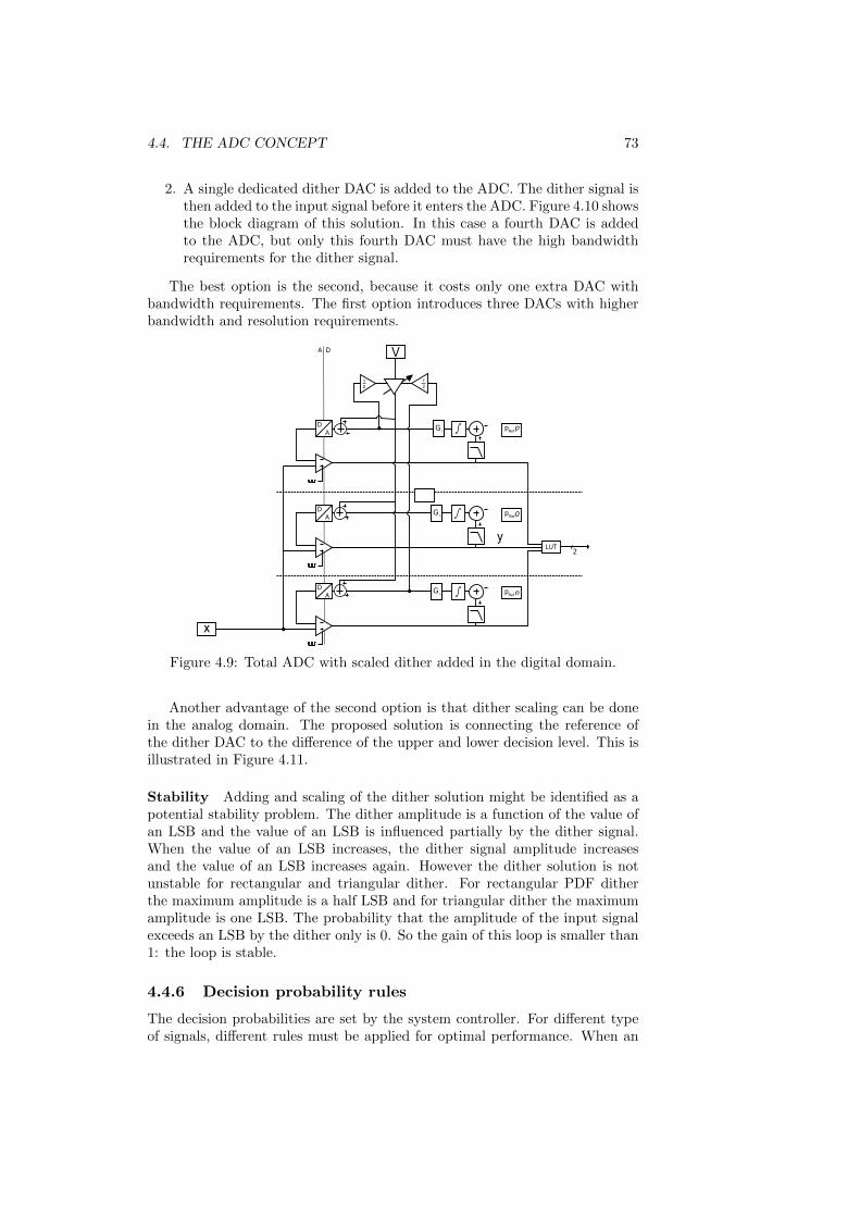
4.4. THE ADC CONCEPT 73
2. A single dedicated dither DAC is added to the ADC. The dither signal isthen added to the input signal before it enters the ADC. Figure 4.10 showsthe block diagram of this solution. In this case a fourth DAC is addedto the ADC, but only this fourth DAC must have the high bandwidthrequirements for the dither signal.
The best option is the second, because it costs only one extra DAC withbandwidth requirements. The first option introduces three DACs with higherbandwidth and resolution requirements.
DA
DA
DA
DA
LUT
x
2
G L
G L
G L
Refp p
Refp 0
Refp n
y
12
12
V
Figure 4.9: Total ADC with scaled dither added in the digital domain.
Another advantage of the second option is that dither scaling can be donein the analog domain. The proposed solution is connecting the reference ofthe dither DAC to the difference of the upper and lower decision level. This isillustrated in Figure 4.11.
Stability Adding and scaling of the dither solution might be identified as apotential stability problem. The dither amplitude is a function of the value ofan LSB and the value of an LSB is influenced partially by the dither signal.When the value of an LSB increases, the dither signal amplitude increasesand the value of an LSB increases again. However the dither solution is notunstable for rectangular and triangular dither. For rectangular PDF ditherthe maximum amplitude is a half LSB and for triangular dither the maximumamplitude is one LSB. The probability that the amplitude of the input signalexceeds an LSB by the dither only is 0. So the gain of this loop is smaller than1: the loop is stable.
4.4.6 Decision probability rules
The decision probabilities are set by the system controller. For different typeof signals, different rules must be applied for optimal performance. When an

74 CHAPTER 4. SYSTEM LEVEL DESIGN
DA
DA
x
DA
DA
LUT2
G L
G L
G L
Refp p
Refp 0
Refp n
DAv
y
12
12
Figure 4.10: Total ADC with scaled dither added to the input signal
DA
DA
Ref+
Ref-
a) b)
Figure 4.11: Scaling the dither while converting to analog domain. b) is theproposed implementation of a)
optimal rule for a specific signal type is applied, the SFDR is largest. For asine wave for instance, the decision level rules are optimal when the ditheredsignal ampltitude exactly spans the input range.
In practice when the ADC is used in the spectrum analyzer, the mostconservative decision probability rules must be applied. Only in that case itcan be guaranteed that distortion components for any type of input signal arebelow the noise floor.
For a sine wave, this conservative setting results in a raised noise floor andthus SFDR is degraded. However, for analyzing the behavior of the ADC, theoptimal rule per signal type can be applied.
This section describes optimal decision probability rules for a sinusoidalsignal and Gaussian distributed signal. Finding optimal decision level rules forother types of signals is a bit more complicated and is briefly addressed (findingoptimal decision rules for these signals is expected to be quite a study and isconsidered out of scope of this thesis):

4.4. THE ADC CONCEPT 75
Decision level rules for a sine wave as input The PDF of a sine wave:
px(x) =1
π ·√A2 − x2
(4.43)
(4.44)
where A is set to 32LSB for rectangular dither and 1LSB for triangular dither.
For rectangular dither:
pv = ΠLSB (4.45)
pwr = px ∗ pv (4.46)
and for triangular dither:
pv = ΠLSB ∗ΠLSB (4.47)
pwt = px ∗ pv (4.48)
Non-linearity is minimized when all the possible input values are within theADC range. The null-decision level must correspond to a probability of 0.5,because of PDF symmetry. The positive decision probability must correspondto half the maximum input value, the negative decision level must correspondto half the minimum input value.
The optimal decision are, for rectangular dither:
p−1w ([
1
2, 0,−1
2]) = [0.2542, 0.5, 0.7457] (4.49)
The optimal decision are, for triangular dither:
p−1w ([
1
2, 0,−1
2]) = [0.1250, 0.5, 0.8750] (4.50)
These results are verified by simulation.The MATLAB snippet for obtaining these rules can be found in Appendix
C.5.1.
Decision level rule for a Gaussian distributed signal A Gaussian dis-tributed signal can have any value theoretically. In practice the input signalrange will be bounded, but a decision level rule for which all the possible inputvalues fall into the ADC range results in a lot of attenuation.
For this decision level rule the percentage of samples falling outside theADC range is chosen such that the SFDR is not degraded to below 40, 50 and60 dB.
A relation between distortion and signal power is determined by simulation.Figure 4.12 shows the relation between the power of a Gaussian distributedsignal and the maximum power of a clipping error frequency component. Theinput signal is shown in Figure 4.13. The simulation is repeated for variousinput signal bandwidths with different locations in the spectrum, yielding ap-proximately the same result. The MATLAB code is listed in Appendix C.5.2.1.
The PDF of the input signal:
px =1√
2πσ2e−
(x−µ)2
2σ2 (4.51)
pw = px ∗ pw (4.52)

76 CHAPTER 4. SYSTEM LEVEL DESIGN
0.12 0.14 0.16 0.18 0.2 0.22 0.24 0.26 0.28 0.3−90
−80
−70
−60
−50
−40
−30
X: 0.146Y: −60.84
�
pow
er[d
B]
X: 0.174Y: −51.11
X: 0.215Y: −40.01
/FS
Figure 4.12: clipping error maximum frequency component power per signalinput power
0 0.2 0.4 0.6 0.8 1−400
−300
−200
−100
0
Pow
er[d
BFs
]
Frequency (fs)
Figure 4.13: Gaussian distributed band-limited input signal.
The input signal power allowed is:
σ(40dB) = 0.215[1
FS] (4.53)
σ(50dB) = 0.174[1
FS] (4.54)
σ(60dB) = 0.146[1
FS] (4.55)
This gives the following decision level probabilities (MATLAB code of ob-taining these number is found in Appendix C.5.2.2):
p(40dB)ref = p−1
w ([1
2, 0,−1
2]) = [0.1354, 0.5, 0.8646] (4.56)
p(50dB)ref = p−1
w ([1
2, 0,−1
2]) = [0.0925, 0.5, 0.9075] (4.57)
p(60dB)ref = p−1
w ([1
2, 0,−1
2]) = [0.0626, 0.5, 0.9374] (4.58)
These decision probabilities differ from the probabilities used in astronomyapplications [8], [7] for reasons explained in section 4.4.1. In those applications

4.4. THE ADC CONCEPT 77
the optimal decision level probabilities are:
∆ = 0.91 · σ (4.59)
p(radioastronomy)ref = CDF−1(−0.91, 0, 0.91) (4.60)
= [0.1814, 0.5, 0.8186] (4.61)
4.4.7 Uncorrelated quantization and dither noise
The performance of the 2-bit AD conversion is increased by utilizing the cross-correlation spectrum analyzer: the quantization and dither noise in the spec-trum is decreased. To achieve this reduction, uncorrelated dither is added toboth parallel signal paths and the dither and quantization noise floor is loweredby cross-correlation and spectral averaging.
In case of an analog front-end with a zero-IF mixer concept, generationof two uncorrelated complex dither signals is done by four dither generators(a,b,c,d):
v1 = va + i · vb (4.62)
v2 = vc + i · vd (4.63)
For a mixer-less concept two dither signals are required, as the dither signalsare not complex.
For each dither signal a dither DAC is required and the signal is scaled tothe LSB of that ADC. Figure 4.14 shows the block schematic of the analog todigital conversion for a zero-IF mixer concept.
loop
loop
loop
lut
dither
loop
loop
loop
lut
dither
0o
90 o
loop
loop
loop
lut
dither
loop
loop
loop
lut
dither
0o
90 o
FFT
FFT
XCOR
DAC
DAC
DAC
DAC
Figure 4.14: ADCs in a total system in case of an FX correlator. Decision levelfeedback to dither DAC, attenuator and averaging not drawn. For each ADCone dither DAC is introduced.
4.4.8 Input signal dependency
During system level design, dependencies of the system performance on theinput signal have been found. Because not all characteristics of the inputsignal are known, the exact impact on system performance is not presented
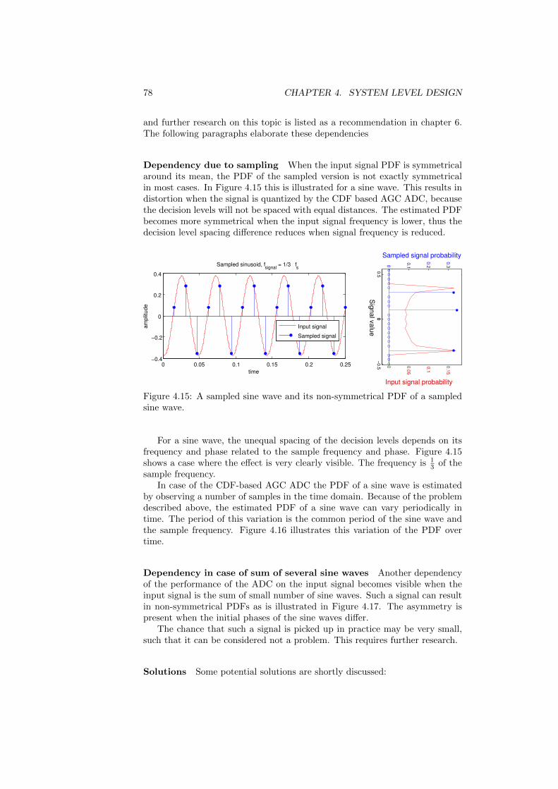
78 CHAPTER 4. SYSTEM LEVEL DESIGN
and further research on this topic is listed as a recommendation in chapter 6.The following paragraphs elaborate these dependencies
Dependency due to sampling When the input signal PDF is symmetricalaround its mean, the PDF of the sampled version is not exactly symmetricalin most cases. In Figure 4.15 this is illustrated for a sine wave. This results indistortion when the signal is quantized by the CDF based AGC ADC, becausethe decision levels will not be spaced with equal distances. The estimated PDFbecomes more symmetrical when the input signal frequency is lower, thus thedecision level spacing difference reduces when signal frequency is reduced.
0 0.05 0.1 0.15 0.2 0.25−0.4
−0.2
0
0.2
0.4
time
ampl
itude
Sampled sinusoid, fsignal = 1/3 fs
Input signal
Sampled signal
−0.5
0
0.5
0 0.05
0.1
0.15
Signalvalue
0
0.1
0.2
0.3
Input signal probability
Sampled signal probability0
Figure 4.15: A sampled sine wave and its non-symmetrical PDF of a sampledsine wave.
For a sine wave, the unequal spacing of the decision levels depends on itsfrequency and phase related to the sample frequency and phase. Figure 4.15shows a case where the effect is very clearly visible. The frequency is 1
3 of thesample frequency.
In case of the CDF-based AGC ADC the PDF of a sine wave is estimatedby observing a number of samples in the time domain. Because of the problemdescribed above, the estimated PDF of a sine wave can vary periodically intime. The period of this variation is the common period of the sine wave andthe sample frequency. Figure 4.16 illustrates this variation of the PDF overtime.
Dependency in case of sum of several sine waves Another dependencyof the performance of the ADC on the input signal becomes visible when theinput signal is the sum of small number of sine waves. Such a signal can resultin non-symmetrical PDFs as is illustrated in Figure 4.17. The asymmetry ispresent when the initial phases of the sine waves differ.
The chance that such a signal is picked up in practice may be very small,such that it can be considered not a problem. This requires further research.
Solutions Some potential solutions are shortly discussed:
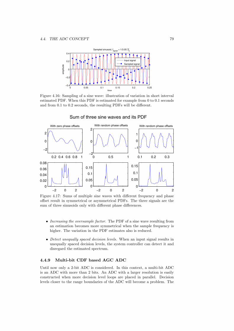
4.4. THE ADC CONCEPT 79
0 0.05 0.1 0.15 0.2 0.25−0.4
−0.2
0
0.2
0.4
time
ampl
itude
Sampled sinusoid, fsignal = 1/3.05 �fs
Input signal
Sampled signal
Figure 4.16: Sampling of a sine wave: illustration of variation in short intervalestimated PDF. When this PDF is estimated for example from 0 to 0.1 secondsand from 0.1 to 0.2 seconds, the resulting PDFs will be different.
0.2 0.4 0.6 0.8 1
−2
0
2
−2 0 20
0.02
0.04
0.06
0.08
0 0.5 1−2
0
2
−2 0 20
0.05
0.1
0.15
0.1 0.2 0.3
−1
0
1
−2 0 20
0.05
0.1
0.15
Sum of three sine waves and its PDF
With zero phase offsets With random phase offsets With random phase offsets
Figure 4.17: Sums of multiple sine waves with different frequency and phaseoffset result in symmetrical or asymmetrical PDFs. The three signals are thesum of three sinusoids only with different phase differences.
• Increasing the oversample factor. The PDF of a sine wave resulting froman estimation becomes more symmetrical when the sample frequency ishigher. The variation in the PDF estimates also is reduced.
• Detect unequally spaced decision levels. When an input signal results inunequally spaced decision levels, the system controller can detect it anddisregard the estimated spectrum.
4.4.9 Multi-bit CDF based AGC ADC
Until now only a 2-bit ADC is considered. In this context, a multi-bit ADCis an ADC with more than 2 bits. An ADC with a larger resolution is easilyconstructed when more decision level loops are placed in parallel. Decisionlevels closer to the range boundaries of the ADC will become a problem. The
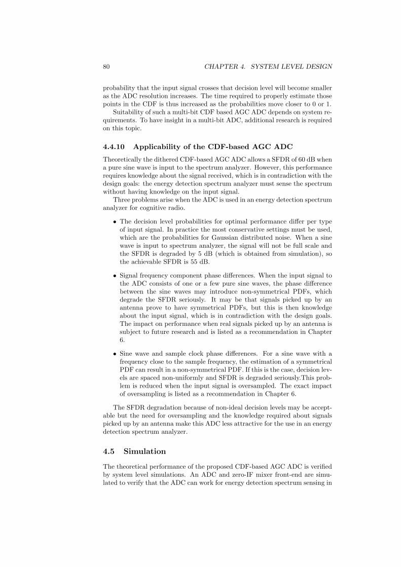
80 CHAPTER 4. SYSTEM LEVEL DESIGN
probability that the input signal crosses that decision level will become smalleras the ADC resolution increases. The time required to properly estimate thosepoints in the CDF is thus increased as the probabilities move closer to 0 or 1.
Suitability of such a multi-bit CDF based AGC ADC depends on system re-quirements. To have insight in a multi-bit ADC, additional research is requiredon this topic.
4.4.10 Applicability of the CDF-based AGC ADC
Theoretically the dithered CDF-based AGC ADC allows a SFDR of 60 dB whena pure sine wave is input to the spectrum analyzer. However, this performancerequires knowledge about the signal received, which is in contradiction with thedesign goals: the energy detection spectrum analyzer must sense the spectrumwithout having knowledge on the input signal.
Three problems arise when the ADC is used in an energy detection spectrumanalyzer for cognitive radio.
• The decision level probabilities for optimal performance differ per typeof input signal. In practice the most conservative settings must be used,which are the probabilities for Gaussian distributed noise. When a sinewave is input to spectrum analyzer, the signal will not be full scale andthe SFDR is degraded by 5 dB (which is obtained from simulation), sothe achievable SFDR is 55 dB.
• Signal frequency component phase differences. When the input signal tothe ADC consists of one or a few pure sine waves, the phase differencebetween the sine waves may introduce non-symmetrical PDFs, whichdegrade the SFDR seriously. It may be that signals picked up by anantenna prove to have symmetrical PDFs, but this is then knowledgeabout the input signal, which is in contradiction with the design goals.The impact on performance when real signals picked up by an antenna issubject to future research and is listed as a recommendation in Chapter6.
• Sine wave and sample clock phase differences. For a sine wave with afrequency close to the sample frequency, the estimation of a symmetricalPDF can result in a non-symmetrical PDF. If this is the case, decision lev-els are spaced non-uniformly and SFDR is degraded seriously.This prob-lem is reduced when the input signal is oversampled. The exact impactof oversampling is listed as a recommendation in Chapter 6.
The SFDR degradation because of non-ideal decision levels may be accept-able but the need for oversampling and the knowledge required about signalspicked up by an antenna make this ADC less attractive for the use in an energydetection spectrum analyzer.
4.5 Simulation
The theoretical performance of the proposed CDF-based AGC ADC is verifiedby system level simulations. An ADC and zero-IF mixer front-end are simu-lated to verify that the ADC can work for energy detection spectrum sensing in

4.5. SIMULATION 81
cognitive radio. The results in the frequency domain are presented as spectraof complex valued signals.
The expected behavior and performance of the ADC are verified by simu-lation using SIMULINK and MATLAB. The decision level loop is built out ofSIMULINK blocks. Input signals are generated in MATLAB and imported inSIMULINK, output signals are exported to and analyzed in MATLAB.
This section consists of two subsections:
1. Functional simulations. The expected function of the ADC is verified.The settling of the ADC is shown and discussed and estimated spectraof different input signals are discussed.
2. Non-linearity simulations. Because the comparator is worked out at sys-tem level in Chapter 5, three sources of additional non-linearity are mod-eled at system level: comparator offset, comparator hysteresis and com-parator noise. Maximum allowed values for these non-linearities are foundas they are expected to be present at the circuit level.
4.5.1 Functional simulations
Following paragraphs show and discuss the simulation results. The time do-main simulation results are shown for a single ADC, as each ADC in the cross-correlation front-end behaves the same. The spectra presented are based on azero-IF mixer concept front-end. I and Q signals are AD converted and thusis the frequency range [− 1
2fs,12fs].
In the following paragraphs three cases are discussed:
1. A sine wave is the input signal, the dither signal has a rectangular PDFand the probabilities are set to the optimal values for a sine wave. Inpractice, for the cognitive radio energy detection spectrum analyzer thesesetting cannot be used, because it is not known whether the signal is asine wave or not.
2. A sine wave is the input signal, the dither signal has a triangular PDFand the probabilities are set to the optimal values for a sine wave.
3. A sine wave is the input signal, the probabilities are set to the optimalvalues for a Gaussian distributed signal. With these settings unacceptableclipping is avoided for sinusoidal or Gaussian distributes signals. Becausethese are the most conservative settings, in practice these setting mustbe used.
4. A Gaussian distributed signal is the input signal.
4.5.1.1 Sine wave input, Rectangular dither, optimal sine waveprobability rules applied
To investigate the SFDR of the loop, a sine wave is used as input signal tothe total ADC. The probability levels for this sine wave are set to the optimalvalues for a sine wave.
Figure 4.24, 4.19 and 4.20 show the result of simulation in SIMULINK.The SFDR in Figure 4.20 is 60.1 dB. The frequency component with strength

82 CHAPTER 4. SYSTEM LEVEL DESIGN
-62.66 dB limits the SFDR. The achieved SFDR is thus 2.5dB lower than thetheoretical SFDR of 62.7 dB.
The settings used for the simulation are shown in Table 4.2. As the decisionlevels climb to their intended levels, the dither signal scales accordingly. Theoutput signal also changes according to the decision levels. The settling timeis about 3.6 · 104 samples: 23.4µs for a sample frequency of 1536MHz. This isonly 0.12% of the measurement time.
0 0.5 1 1.5 2 2.5 3 3.5 4 4.5 5
x 104
−0.4
−0.2
0
0.2
0.4
0.6
0.8
Samples
Am
plitu
de
Inputsignal
OutputSignal
Decision level n
Decision level 0
Descision level p
Figure 4.18: Settling of the ADC, settings used shown in Table 4.2. The inputsignal shown is the input signal at each comparator.
0 1 2 3 4 5 6
x 104
−0.1
−0.05
0
0.05
0.1
Samples
Amplitude
Rectangular dither signal, scaled to one LSB
Figure 4.19: Scaled rectangular dither signal, settings used shown in Table 4.2
−0.5 0 0.5−150
−100
−50
0X: 0.03125Y: −2.531
Pow
er [d
BF
s]
frequency [fs]
X: 0.0001795Y: −62.66
Figure 4.20: Spectrum of quantized sine wave, settings used shown in Table4.2

4.5. SIMULATION 83
Observations The non-linearity effects as discussed in Section 4.4.4.5 canbe seen in this simulation. The simulation shows a CDF step response. Thisis because the initial state of the loop does not corresponds with the CDF ofthe input signal. The effects which can be seen are elaborated:
• The comparator output is limited,so the maximum slope of a decisionlevel is limited. The gain of the comparator of the lower decision levelis smaller, because the target decision level voltage is closer to the lowoutput voltage of the comparator.
• The dither signal amplitude has more relative overshoot than either ofthe decision levels. The upper decision level increases faster than thelower, such that the difference signal has more overshoot.
Spectrum averaged XC result, long measurement time Figure 4.21shows the simulation result of the full measurement time of 0.2 seconds. TheSFDR is 58.2 dB.
−0.5 0 0.5−80
−60
−40
−20
0X: 0.03125Y: −2.499
X: −0.01562Y: −60.74
− Sine wave input, single ADC result, 199.6808 ms measurement time −Cross−correlated spectrum, 256 channels
Relative frequency [fs]
Power[dBFs]
Figure 4.21: Total IF front-end simulation, spectrum (when settled), settingsused shown in Table 4.2
4.5.1.2 Sine wave input, triangular dither, optimal probabilityrules applied
When triangular dither is used, the result is as expected: the noise floor ishigher and the settling time is longer. Figure 4.22 shows the settling of oneADC. When the system would be implemented and the positive voltage is 1volt, then for this input signal, dither signal and loop settings, the input signalto the ADC would clip. The dither is amplified such that the sum of theinput signal and the dither leads to values outside the range of supply voltage.Figure 4.23 shows simulation results when the clipping is modeled. Nothing haschanged, because the input signal is above the upper decision level, whether itis being clipped or not: the ADC output does not change.

84 CHAPTER 4. SYSTEM LEVEL DESIGN
Setting Value
Input signal Sample clock 1.536 GHzInput signal type Sine waveInput signal frequency 48 MHzInput signal offset 0.65Input signal amplitude 0.15Dither signal Rectangularpn 0.75p0 0.5pp 0.25Hlpf
1s·6·10−5+1
Gl 3 · 105
Table 4.2: Simulation settings for ADC simulation
1 2 3 4 5 6 7 8
x 104
−0.2
0
0.2
0.4
0.6
0.8
1
Samples
Am
plitu
de
Decision level n
Decision level 0
Descision level p
Figure 4.22: Settling of the ADC, settings used shown in Table 4.3
2 4 6 8 10
x 104
0
0.5
1
Samples
Am
plitu
de Inputsignal
OutputSignal
Decision level n
Decision level 0
Descision level p
Figure 4.23: Clipping of input signal while settling. 4.3

4.5. SIMULATION 85
Setting Value
Input signal Sample clock 1.536 GHzInput signal type Sine waveInput signal frequency 48 MHzInput signal offset 0.65Input signal amplitude 0.15Dither signal Triangularpn 0.875p0 0.5pp 0.125Hlpf
1s·6·10−5+1
Gl 3 · 105
Table 4.3: Simulation settings for ADC simulation
4.5.1.3 Sine wave input, optimal Gaussian distribution probabilityrules applied
When the probability are set to the optimal probabilities for a Gaussian dis-tributed signal, the power of the sine wave is reduced by 5.2 dB and the settlingtime has increased to
Setting Value
Input signal Sample clock 1.536 GHzInput signal type Sine waveInput signal frequency 48 MHzInput signal offset 0.65Input signal amplitude 0.1pn 0..09374p0 0.5pp 0.0626Hlpf
1s·6·10−5+1
Gl 3 · 105
Table 4.4: Simulation settings for ADC simulation
4.5.1.4 Gaussian distributed signal input
The simulation results in case of sinusoidal signals at the input show a smallerresolution bandwidth then the intended 6 MHz. This is done to show thatno harmonic distortion components appear in the spectrum, while limiting thesimulation time. For a Gaussian distributed signal, this cannot be done becausedue to the wide input signal bandwidth, the distortion components are a lotmore distributed across the spectrum.
Figure 4.27 shows the result of simulations in SIMULINK. The decisionlevels are set for no distortion components above -60 dBFs (obtained in Section4.4.6).

86 CHAPTER 4. SYSTEM LEVEL DESIGN
0 2 4 6 8 10 12x 104
−0.2
0
0.2
0.4
0.6
0.8
Samples
Am
plitu
de
Decision level n
Decision level 0
Descision level pOutput signal
Input signal
Figure 4.24: Total ADC simulation, settings used shown in Table 4.4
2 4 6 8 10 12x 104
−0.15
−0.1
−0.05
0
0.05
0.1
0.15
0.2
Samples
Am
plitu
de
Figure 4.25: Scaled dither signal, settings used shown in Table 4.4
−0.5 0 0.5−150
−100
−50
0
X: 0.1079Y: −62.92
X: 0.03125Y: −7.686
Pow
er [d
BF
s]
frequency [fs]
SFDR:55.0726
Figure 4.26: Spectrum when ADC is settled, The fundamental tone now has aamplitude of -7.7 dBFs. Settings used shown in Table 4.4

4.5. SIMULATION 87
The settling time in this case is about 6 · 104 samples: 39µs for a samplefrequency of 1536MHz.
The settings used for the simulation are shown in Table 4.5. The settlingtime per decision level is different than in the case of a sine wave, resulting inmore overshoot of the dither signal amplitude.
The spectrum of this short measurement time simulation is not shown, be-cause it does not give a lot of information. In the case of a Gaussian distributedsignal, reducing the resolution bandwidth does not provide more information.
In the following paragraph, the resulting spectrum is presented when themeasurement time is increased.
Setting Value
Input signal Sample clock 1.536 GHzInput signal type Gaussian distributedInput signal frequency 64-96 MHzInput signal offset 0.65Input signal power 0.0466pn 0.9374p0 0.5pp 0.0626Hlpf
1s·6·10−5+1
Gl 3 · 105
Table 4.5: Simulation settings for ADC simulation
0 2 4 6 8 10 12 14x 104
−0.4
−0.2
0
0.2
0.4
0.6
0.8
1
Samples
Am
plitu
de
Inputsignal
OutputSignal
Decision level n
Decision level 0
Descision level p
Figure 4.27: Gaussian distributed signal, settling behavior. Settings shown inTable 4.5.
Spectrum averaged XC result, long measurement time Figure 4.28shows the result of a simulation of the full measurement time of 0.18 seconds.It is clearly seen that the resulting spectrum noise floor is non-white. Thestrongest distortion components are located at −3 times the fundamental tonefrequencies. The non-whiteness of the noise floor is because of the clippingnoise which is present. It is interesting to note that the distortion components
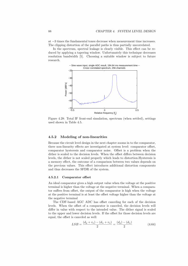
88 CHAPTER 4. SYSTEM LEVEL DESIGN
at −3 times the fundamental tones decrease when measurement time increases.The clipping distortion of the parallel paths is thus partially uncorrelated.
In the spectrum, spectral leakage is clearly visible. This effect can be re-duced by applying a tapering window. Unfortunately this technique decreasesresolution bandwidth [5]. Choosing a suitable window is subject to futureresearch.
−0.5 0 0.5−70
−60
−50
−40
−30
−20
− Sine wave input, single ADC result, 184.64 ms measurement time −Cross−correlated spectrum, 256 channels
Relative frequency [fs]
Pow
er [d
BF
s]
Figure 4.28: Total IF front-end simulation, spectrum (when settled), settingsused shown in Table 4.5.
4.5.2 Modeling of non-linearities
Because the circuit level design in the next chapter zooms in to the comparator,three non-linearity effects are investigated at system level: comparator offset,comparator hysteresis and comparator noise. Offset is a problem when thedither is scaled to the decision levels. When the offset differs between decisionlevels, the dither is not scaled properly which leads to distortion.Hysteresis isa memory effect, the outcome of a comparison between two values depends onthe previous values. This effect introduces additional distortion componentsand thus decreases the SFDR of the system.
4.5.2.1 Comparator offset
An ideal comparator gives a high output value when the voltage at the positiveterminal is higher than the voltage at the negative terminal. When a compara-tor suffers from offset, the output of the comparator is high when the voltageat the positive terminal is at least the offset voltage higher than the voltage atthe negative terminal
The CDF-based AGC ADC has offset canceling for each of the decisionlevels. When the offset of a comparator is canceled, the decision levels willdiffer in value with respect to the intended value. The dither signal is scaledto the upper and lower decision levels. If the offset for those decision levels areequal, the offset is canceled as well:
LSB =(dp + vo)− (dn + vo)
2=
(dp)− (dn)
2(4.64)

4.5. SIMULATION 89
Where dp and dn denote the input voltages at negative terminals of the upperand lower comparator of the ADC. vo denotes the offset voltage. When theupper and lower decision levels have different offsets, the dither range deviatesby half the difference in offset:
LSB =(dp + vop)− (dn + von)
2=
(dp)− (dn)
2+vop − von
2(4.65)
where vop and von denote the offset voltages for the upper and lower compara-tors respectively. In this case the dither range is not equal to one LSB and willcause additional distortion.
It may seem a plausible countermeasure to increase the dither signal rangesuch that the range of the dither is larger than decision level spacing in anycase. However, the conditions for independent moments and spectral whitenessof Section 3.3 are not satisfied.
Also simulation results show that the added distortion is not reduced bythis countermeasure: would there be no offset in the system, increasing thedither range not only leads to more noise but also to additional distortion.
Allowed offsets Offsets are canceled without SFDR degradation when eachcomparator in the ADC has equal offsets. So only offset-mismatch is lookedat: comparator offset relative to the other comparator offsets. In case of offset-mismatch, the dither signal is not scaled properly to an LSB. Allowed offsetvalues are obtained by simulation.
DA
DA
x
DA
DA
LUT2
G L
G L
G L
Refp p
Refp 0
Refp n
DAv
y
12
12
vo0
vop
Figure 4.29: Total ADC with offsets added to upper and middle comparator.
Three comparators give two relative offsets. In this case the offset of thelower comparator is fixed and the other two are varied. The comparator offsetsare denoted by [von, vo0, vop] and von = 0. For a SFDR of 60 dB the allowedoffsets are found by simulation. Figure 4.29 shows the simulation set up. Theoffset is swept and the maximum allowed value is found for which the distortioncomponents in the resulting spectra are below 60 [dBFs].

90 CHAPTER 4. SYSTEM LEVEL DESIGN
1. vo(0) = vo(p) and vo(0, p) > 0: The resulting dither amplitude is toolarge. Allowed offset: vo(0, p) < 1mV
2. vo(0) = vo(p) and vo(0, p) < 0: The resulting dither amplitude is toosmall. Allowed offset: vo(0,p) > −0.7mV
These numbers are a starting point for circuit level design optimization.
4.5.2.2 Comparator hysteresis
Hysteresis is defined as the maximum difference in the values of a code transi-tion, when the transition level is approached by a changing input signal fromeither side of the transition [21]. Hysteresis is non-linear effect, so distortioncomponents in the spectrum are expected. In many applications hysteresis isdeliberately added to a comparator to get stable output signals: when the dif-ference voltage at the comparator is very small, the noise in the signal causesan fast alternating output. For the CDF-based AGC ADC the essential infor-mation is contained in the statistics of the fast alternating comparator output.Therefore, the hysteresis must be as small as possible.
Hysteresis is subdivided in dynamic and static hysteresis effects. Dynamichysteresis is the non-linearity which depends on input signal frequency. Statichysteresis is caused by memory effects which exist at circuit level. Allowedstatic hysteresis values are obtained by system level modeling of the hysteresiseffects. In this case only static hysteresis effects are modeled, because dynamichysteresis effects depend on the exact implementation of the comparator. Statichysteresis is modeled as:
wh(n) = w(n) + h · 2 · (wh(n− 1)− 1
2) (4.66)
w(n) is the original comparator input sample at moment n, wh is the changedinput sample due to the hysteresis and h is the allowed hysteresis. The outputis thus wh compared to the decision level. Figure 4.30 shows the modeling ofthe hysteresis effect.
In
DA
G L Refp 0
0.5
h 2
[0,1]Out
Figure 4.30: Model of decision level loop with comparator with hysteresis effect.
The allowed value for h is determined by simulation. A SFDR of at least60 dB is achieved when:
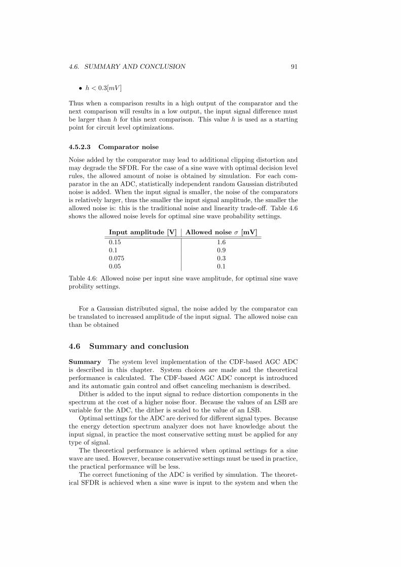
4.6. SUMMARY AND CONCLUSION 91
• h < 0.3[mV ]
Thus when a comparison results in a high output of the comparator and thenext comparison will results in a low output, the input signal difference mustbe larger than h for this next comparison. This value h is used as a startingpoint for circuit level optimizations.
4.5.2.3 Comparator noise
Noise added by the comparator may lead to additional clipping distortion andmay degrade the SFDR. For the case of a sine wave with optimal decision levelrules, the allowed amount of noise is obtained by simulation. For each com-parator in the an ADC, statistically independent random Gaussian distributednoise is added. When the input signal is smaller, the noise of the comparatorsis relatively larger, thus the smaller the input signal amplitude, the smaller theallowed noise is: this is the traditional noise and linearity trade-off. Table 4.6shows the allowed noise levels for optimal sine wave probability settings.
Input amplitude [V] Allowed noise σ [mV]
0.15 1.60.1 0.90.075 0.30.05 0.1
Table 4.6: Allowed noise per input sine wave amplitude, for optimal sine waveprobility settings.
For a Gaussian distributed signal, the noise added by the comparator canbe translated to increased amplitude of the input signal. The allowed noise canthan be obtained
4.6 Summary and conclusion
Summary The system level implementation of the CDF-based AGC ADCis described in this chapter. System choices are made and the theoreticalperformance is calculated. The CDF-based AGC ADC concept is introducedand its automatic gain control and offset canceling mechanism is described.
Dither is added to the input signal to reduce distortion components in thespectrum at the cost of a higher noise floor. Because the values of an LSB arevariable for the ADC, the dither is scaled to the value of an LSB.
Optimal settings for the ADC are derived for different signal types. Becausethe energy detection spectrum analyzer does not have knowledge about theinput signal, in practice the most conservative setting must be applied for anytype of signal.
The theoretical performance is achieved when optimal settings for a sinewave are used. However, because conservative settings must be used in practice,the practical performance will be less.
The correct functioning of the ADC is verified by simulation. The theoret-ical SFDR is achieved when a sine wave is input to the system and when the
92 CHAPTER 4. SYSTEM LEVEL DESIGN
corresponding optimal settings are used. With the most conservative settings,the SFDR is decreased by 5.2 dB.
During this verification, the assumption of the input signal having a sym-metrical PDF appeared to be a problem. When several strong narrow-bandsignals are present in the input signal, the PDF becomes non-symmetrical.Also the frequency and phase of narrow-band input signals related to the sam-ple frequency and phase influence the performance. For sinusoidal signals withfrequencies close to the sample frequency, the sampled version of the signal hasa non-symmetrical or slowly varying non-symmetrical PDF.
The performance of the ADC thus depends on the input signal. For largeroversample factors this dependency reduces and the practical performance ap-proximates the theoretical performance (for equal system settings).
When the practical performance is reduced by the non-uniform decisionlevel spacing, this can be detected by a system controller. Thus, when themeasurement is corrupted due to this effect, it is known by the system controllerand the spectrum can be disregarded, although this is not acceptable in acognitive radio application.
The ADC is simulated to verify the expected behavior of the ADC andto see if the theoretical SFDR can be achieved. The dither signals addedto the (quadrature mixing) cross-correlation IF front-end are two statisticallyindependent (complex) uniform distributed random signals. This allows thecross-correlation to reduce the dither and quantization noise floor. Thus ahigher SFDR is possible than would be possible for a conventional ditheredADC with the same dither resolution, quantization resolution and resolutionbandwidth.
Because the comparator is analyzed on circuit level, hysteresis and offsetare modeled at system level, as they are expected circuit level non-linearities.This way maximum allowed values are obtained.
With this system level design, the performance dependencies at system levelare investigated and circuit level components, such as the comparator, can beimplemented on circuit level.
Conclusions When the resolution of the ADCs for a cognitive radio spec-trum analyser is lowered, several problems are introduced. The ADC proposedin this chapter is able to tackle those problems, but other problems appear.
The problem of distortion due to the low resolution is reduced by addingdither to the input signal. The result is that the measurement noise flooris raised. This problem is reduced by utilizing the cross-correlation concept,thus the measurement noise floor is lowered by increasing measurement time.To do this two statistically independent dither signals with specific PDFs arerequired, which must be generated in the digital domain. The dither signalmust be added to the analog input signal, thus additional hardware is requiredto convert this digital signal to the analog domain.
Another problem is, to achieve maximal SFDR, signal clipping must beavoided or limited to acceptable values. The CDF-based AGC ADC solvesthis problem by the AGC and offset canceling. These features are realizedby adjustable ADC decision levels based on the CDF estimate of the inputsignal. This approach introduces new problems. Due to the coarse estimationof CDF, different signals cannot be distinguished. Thus in practice, the most

4.6. SUMMARY AND CONCLUSION 93
conservative ADC settings must be used, which decreases the sensitivity ofthe spectrum analyzer. An assumption was made that input signal PDFs aresymmetrical, but the estimate of a symmetrical PDF can be non-symmetrical.This is the case for input signals with frequencies close to half the samplefrequeny. The assumption may be not realistic as the PDF of a sum of a fewstrong sinusoids can be non-symmetrical.
Digitally dithering a 2-bit ADC is an effective way to increase its SFDR.When decision levels are varried to create AGC and offset canceling, the dithercan be scaled accordingly to approximate the theoretical allowed performance.The utilization of the cross-correlation concept and statistically independentdigitally generated dither effectively increases the SFDR of the dithered ADCat the cost of measurement time.
The AGC and offset canceling realization of the CDF-based AGC ADC,introduces problems which counteract the design goals of the energy detectionspectrum analyzer. Because of the dependency of performance on the inputsignal, the CDF-based AGC and offset canceling is not considered to be a goodchoice for a cognitive radio energy detection spectrum analyzer. The scaleddithering and cross-correlation utilization can be applied to 2-bit ADCs withother AGC mechanism, such as in [7].


Chapter 5
Circuit level design
The previous chapters described the system level design and the theory requiredto make proper design choices. To have insight in the impact of implementingthe ADC components on circuit level, the most critical component is selectedand implemented. The comparator is implemented in Cadence using UMC090MOSFETs. This is a 90 nm process with 1v supply voltage MOSFETs, themodels used are BSIM4 models. The first part of this chapter describes thecomparator, how it works and the expected causes for performance degradation.The second part presents ADC simulation results with ideal components exceptfor the comparator. The comparator is worked out for a sample frequency of1.536 MHz.
5.1 Critical ADC component
The ADC consists of the following blocks in the analog domain:
1. Comparator, sample frequency: 1536 MHz
2. Dither DAC, resolution: 6 bits, frequency: 1536 MHz
3. Decision level DAC, 8 bits, frequency: 3 MHz
DACs with requirements compaale to the dither DAC are found in litera-ture and is considered to be not critical, Table 5.3 gives an overview of someDAC characteristics from literature. The decision level DAC has a relative lowoutput frequency and is even less critical. The comparator is more critical.In system level design, the influence of offset, hysteresis and common-modedependency became clear. To get a view on the influences of an implementedcomparator on the system performance by these factors, a comparator is se-lected and implemented on circuit level. The selected comparator is previouslyimplemented for the use for long on-chip wires and the specifications are in thesame range as the target comparator.
The comparator may not have too much hysteresis, which adds distortionto the measured spectrum of the energy detection spectrum analyzer. Whenits offset is too large the effect of dither is reduced and distortion componentsappear. Also power estimation becomes a problem when the offset depends onthe input common mode voltage.
95

96 CHAPTER 5. CIRCUIT LEVEL DESIGN
Reference Resolution sample rate Power process year
[31] 6 Bits 1.25 GHz 6 mW 1.8 V, 0.18 um 2008[32] 6 Bits 2.7 GHz 28 mW 1.2V, 0.13 um 2006[33] 6 Bits 5.4 GHz 20 mW 1.5V, 0.13 um 2005[34] 6 Bits 1 GHz 7.5 mW 1.5 V,0.13 um 2005
Table 5.1: CMOS DAC characteristics from literature.
5.2 The comparator
The selected comparator is the double tail voltage sense amplifier by D. Schinkelet. al.[35]. The implementation described in [35] allows a sample frequency ofup to 3 GHz, fabricated in a 1.2V 90nm CMOS process. The comparator wasdesigned for being a part of a low-swing on-chip data transceiver, with inputsignals biased around 1.1V . The operating characteristics thus differ from theones in this thesis.
5.2.1 The circuit
Figure 5.2 shows the comparator used in the circuit level modeling. It is aclocked comparator, each half period it is reset and the next half period itcompares the input signals. The parasitic capacitances play a crucial role inthe way the comparator functions. Therefore figure 5.2 shows the comparatorwith parasitic capacitances connected to the internal nodes and the negativesupply rail.
Both phases are described in next paragraphs.
Clk Clk
In+ In-
Clk
Di- Di+
Di+Di-
Clk
Out+Out-
M12
M1
M2
M3
M4
M10 M11
M7
M9
M8
M5 M6
Figure 5.1: Double tail voltage sense amplifier [35], consisting of an input stage(left) and a latch (right).
Reset phase. When the Clk signal is low, nodes Di− and Di+ are connectedto the positive supply rail and CDi− and CDi− are charged. As a result M10and M11 start conducting and will discharge COut− and COut+. M12 and M9are not conducting during reset.
Compare phase. Nodes Di− and Di+ are ‘high‘ and nodes Out+ and Out−are ‘low‘. At the rising edge of the Clk signal, M9 starts to conduct and the

5.2. THE COMPARATOR 97
Clk Clk
In+ In-
Clk
Di- Di+
Di+Di-
Clk
Out+Out-
M12
M1
M2
M3
M4
M10 M11Out-COut+C
Di-C Di+C
M7 M8
M9
M5 M6
Figure 5.2: Comparator with parasitic capacitances.
voltages on In+ and In− will make M5 and for M6 conduct. As a result nodesDi− and Di+ are discharged to the negative supply rail with a rate dependingon the input voltages.
The resulting voltage difference on nodes Di− and Di+ cause differentcurrents through M10 and M11. One of the output nodes will discharge fasterand the positive feedback of the latch amplifies this difference such that oneoutput node will be pulled to the negative supply rail and one to the positivesupply rail.
Figure 5.3 shows the Di and output nodes of the comparator.
0 200 400 600 800
0
0.5
1
Output nodes
time [ps]
Vol
tage
[V]
Out+
Out−
0 200 400 600 800
0
0.5
1
time [ps]
Vol
tage
[V]
Di+
Di−
1 2 1 2
Figure 5.3: Internal and output nodes of comparator for a voltage difference of150 mV. 1) reset phase. 2) compare phase
5.2.2 Input signal properties
Because the input MOSFETs are N type devices, the input signal is biased suchthat the input MOSFETs are in strong inversion. The input signal swing....
5.2.3 Block diagram
To have insight in the behavior of the comparator during the compare phase,a block diagram is derived, which shown in Figure 5.4. This block diagramshows the location of gain and the integrations. When the differential paths are

98 CHAPTER 5. CIRCUIT LEVEL DESIGN
assumed to be perfectly symmetrical, the comparator behavior can be depictedas shown in Figure 5.5 (this block diagram is also presented by D. Schinkel ona poster at ICD). The gain blocks do not have a fixed gain, thus the blockdiagram does not represent a linear model of the comparator.
cs1
cs1
IM10
I M11I M1,M2
I M3,M4
VOut+
VOut-
cs1 VDi-I M5Vin+
cs1VDi- I M6 Vin-
M10M5 M3,M4
M1,M2 M11 M6
Figure 5.4: Block diagram representation of comparator
cs1
IVOut
cs1 VDiVin I
I
Figure 5.5: Block diagram representation of comparator, assuming perfect sym-metry between parallel branches.
5.2.4 Dimensioning the comparator
To aim at minimal silicon area, the components of the comparator are ini-tially sized with the minimal values allowed by the process. The necessaryadjustments are made for proper operation. For convenient description thecomparator components are grouped:
1. Latch: M1, M2, M3, M4
2. Input stage: M5, M6
3. Input stage reset MOSFETs: M7, M8
4. Input stage tail MOSFET: M9.
5. Intermediate stage: M10, M11
6. Latch top MOSFET: M12
Following paragraphs describe the considerations which are taken into ac-count when the comparator is dimensioned.
Compare phase Component sizes influence the behavior of the comparatorin the compare phase. The following list important aspects when the compara-tor components are dimensioned.
1 Wider MOSFETs increase power consumption due to larger currents andlarge parasitic capacitances which need to be charged and discharged.

5.2. THE COMPARATOR 99
2 For the comparator the input signal is integrated and the integrationsaturates at some point, so that the input MOSFETs (M5, M6) gainshould not be too large. Would the gain be too large, the integration atthe Di nodes saturate and the voltage difference on these nodes is reducedquickly. As a result, the voltage difference due to the integration at theoutput nodes is then limited. Because of the large input signal swing, thesaturation point in time depends on the common mode voltage. For worstcase, the saturation moment must be controlled such that it is within thecompare phase time.
3 The latch (M1, M2, M3, M4) gain should not be too large with respectto the gain of the intermediate MOSFETs (M10, M11). Then the com-parator decision would be influenced by the voltages at the imperfectlydischarged output nodes too much, i.e. hysteresis is increased. The inter-mediate stage gain trades-off to the latch gain. Larger intermediate phasegain reduces hysteresis, but it takes longer for the latch to determine theoutput voltages.
4 The Di node integration must saturate at the end of the compare phasetime, because at the end of the phase one output must be high andtherefore the intermediate MOSFETs (M10,M11) must not conduct.
5 To reduce the common mode dependency, the WL of the input stage tail
MOSFET (M9) can be decreased such that the MOSFET will act as adegeneration load to the common-source input phase. The gain of theinput stages is then reduced.
6 To let the inverters of the latch (M1, M2, M3, M4) operate properly,in the compare phase the PMOS source voltages must be equal to thepositive supply rail. M12 must be wide enough to supply the currentwhich is conducted by the latch PMOSs. M12 must be approximatelytwo times wider than M2 and M4.
Reset phase In the reset phase all comparator nodes are set to a specificvalue: all parasitic capacitances are (dis)charged. When this is not properlydone, hysteresis is present. The Di nodes and output nodes are (dis)charged:
7 The Di nodes are charged such that the voltage is equal to the posi-tive supply rail at the end of the reset phase. At the start of the resetphase both nodes will be approximately equal to the negative supply rail.Therefore, the Di nodes will not cause much hysteresis.
8 The output nodes are discharged. One of the nodes is approximatelyequal to the positive supply rail. When the output nodes are dischargedin the reset phase, improper discharging will cause hysteresis.
9 The discharge current is limited by the intermediate phase MOSFETs(M10, M11). Di is their gate-source voltage, so when Di are not chargedfast enough, the output nodes are discharged even worse.

100 CHAPTER 5. CIRCUIT LEVEL DESIGN
5.2.4.1 Sizes
Based on the above performance dependencies, the following adjustments aremade to the minimal sized MOSFETs:
1. LATCH PMOSs are sized 3 times wider than the latch NMOSs, to com-pensate for the electron and hole mobility difference.
2. The Latch top PMOS is size 2 times wider than the latch PMOSs, suchthat the source voltage is largely independent of the currents.
3. The input phase tail NMOS is made longer, such that it acts as a degener-ation impedance. Figure 5.6 shows the effect of a longer input phase tailNMOS. Not only the dependency of offset due to mismatch on commonmode voltage is reduced, but also the absolute offset is reduced.
0.4 0.5 0.6 0.7 0.8 0.9 1−0.012
−0.01
−0.008
−0.006
−0.004
−0.002
0
Common mode voltage [V]
Offset
voltage
[V]
Common mode dependent offsetoffset introduced by 10% mismatch of input NMOSs
360 nM180 nM90 nM
Figure 5.6: Illustration of common mode dependent offset. The offset is in-troduced by increasing the length of M5 by 10%. In the plot the three linescorrespond to the three lengths of the input phase tail NMOS (M9).
Table 5.2 lists the component sizes.
Component Width [nm] Length [nm]
M1 120 90M2 360 90M3 120 90M4 360 90M5 120 90M6 120 90M7 120 90M8 120 90M9 120 360M10 120 90M11 120 90M12 720 90
Table 5.2: Comparator MOSFET Sizes
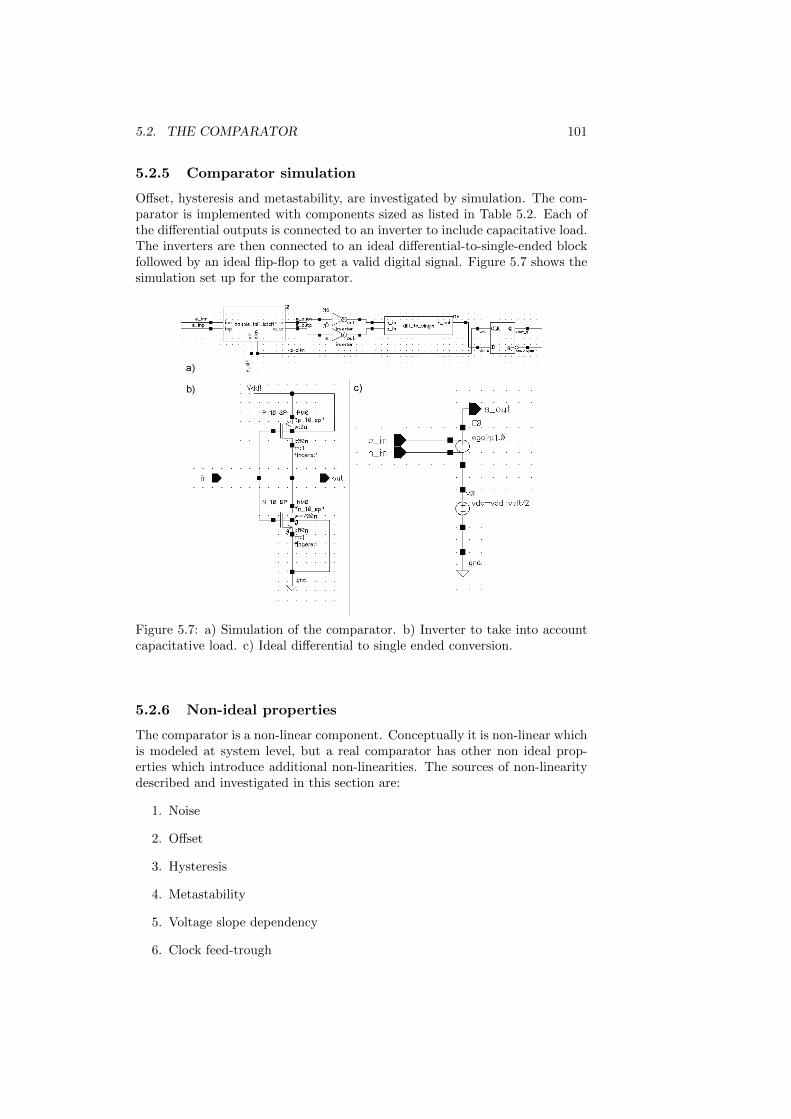
5.2. THE COMPARATOR 101
5.2.5 Comparator simulation
Offset, hysteresis and metastability, are investigated by simulation. The com-parator is implemented with components sized as listed in Table 5.2. Each ofthe differential outputs is connected to an inverter to include capacitative load.The inverters are then connected to an ideal differential-to-single-ended blockfollowed by an ideal flip-flop to get a valid digital signal. Figure 5.7 shows thesimulation set up for the comparator.
Figure 5.7: a) Simulation of the comparator. b) Inverter to take into accountcapacitative load. c) Ideal differential to single ended conversion.
5.2.6 Non-ideal properties
The comparator is a non-linear component. Conceptually it is non-linear whichis modeled at system level, but a real comparator has other non ideal prop-erties which introduce additional non-linearities. The sources of non-linearitydescribed and investigated in this section are:
1. Noise
2. Offset
3. Hysteresis
4. Metastability
5. Voltage slope dependency
6. Clock feed-trough

102 CHAPTER 5. CIRCUIT LEVEL DESIGN
5.2.6.1 Noise
Noise is added to each node by the components of the comparator. The inputsignal to the comparator is dithered and the system it is used in extracts itsinformation from output signal statistics, so noise may seem to be not problem.However, with the optimal probability rules for a sine wave and a sine waveamplitude of 150 mV, clipping may occur which results in distortion. Onthe system level a maximum input referred standard deviation for zero-meanGaussian distributed noise is derived for this case, which is 1.6 mV. This valueis worst case, because for practically more relevant settings the allowed noiseis larger. So worst case, the comparator noise must not exceed this value.
The analysis of noise in a clocked comparator is not as straightforward asthe usual steady-state analysis for amplifiers [36]. In [37] the effect of noiseis analyzed for a latched comparator. The comparator operation is describedby identifying 3 phases and for each phase the noise effects are calculated. Toknow the noise of the double tail voltage sense amplifier, a similar analysis isrequired. For this thesis such an analysis does not fit in the time budget and islisted in the recommendation section in Chapter 6. A standard deviation of theinput referred noise of 1 mV is presented in [37], although device dimensionsare not presented. The comparator is comparable to the double tail voltagesense amplifier. Both comparators are designed for the use in an integratedADC realized in a 90 nM process.
5.2.6.2 Offset
Offsets in the comparator are canceled by the ADC, but the dither signal isimproperly scaled when the offsets of the comparators in the ADC differ toomuch.
The comparator is fully differential, thus offsets are only present because ofcomponent mismatch. In the case of mismatch one of the differential brancheswill be slightly different than the other. The resulting offset will be dependingon the common mode voltage of the input signal. Thus the worst case offsetmust be controlled to be within the allowed value.
Investigation by simulation The dependency of the offsets on commonmode is investigated by the circuit shown in Figure 5.8;
G
D Q
1
Vcm
Vcm
Figure 5.8: Test-bench for investigating offset
The allowed offset difference is 0.7mV . Based on process spread informa-tion, the latch PMOS area can be increased and proper precautions can be

5.2. THE COMPARATOR 103
0.4 0.5 0.6 0.7 0.8 0.9 1−0.03
−0.025
−0.02
−0.015
−0.01
−0.005
0
0.005
Common mode voltage [V]
Offs
etvo
ltage
[mV
]
M1
M10
M6
M8
M2
Figure 5.9: Common mode dependent offset for 5nM difference in MOSFETlength for components shown in figure 5.2.
taken during layout [38], such that the expected mismatch does not degradeSFDR too much.
5.2.6.3 Hysteresis
Hysteresis is present when the reset transistors do not fully discharge the para-sitic capacitances of the Di and output nodes. The CDi parasitic capacitancesare both discharged in the compare phase and charged in the reset phase.Therefore there will be hardly any difference voltage at these nodes at the endof the compare phase, when the capacitances are not fully charged in the resetphase. So the contribution to hysteresis is considered negligible.
The output nodes have opposite voltages after the compare phase. Whenthe capacitor is not fully discharged, one output node will have charge left atthe start of the compare phase. Therefore the output node parasitic capaci-tances are dominant in determining the hysteresis. It is thus important thatthe load capacitance of the comparator is taken into account when hysteresisdependency is analyzed.
Investigation by simulation In reset the intermediate phase MOSFETs(M10, M11) will reset the output nodes. So the input phase reset transistors(M7, M8) must pull the Di nodes high fast enough such that the intermediatetransistors pull the output nodes low fast enough. The minimal sized transis-tors appear to be sufficient for the comparator. Figure 5.10 shows the behaviorof the comparator for very large common mode and little differential modeinput signal. One clock period the input voltage difference is 200 mV and thenext period it is only 1 mV. For this worst case input signal, the output nodesare reset properly. The difference voltage at the output nodes is smaller than1uV . The hysteresis effect is thus obscured by noise and assumed to be not ofany influence.
5.2.6.4 Metastability
The problem of metastability for a comparator is that for very small inputvoltage differences, the output does not reach a valid logic output voltage in

104 CHAPTER 5. CIRCUIT LEVEL DESIGN
0 0.2 0.4 0.6 0.8 1 1.2 1.4 1.6 1.8−0.2
0
0.2
0.4
0.6
0.8
1
1.2
Time [ns]
Vol
tage
[V]
Out+
Out−
In−
In+
Di+
Di−
Figure 5.10: Static hysteresis is obscured by noise and not degrading the per-formance below toleration. The Di and output nodes are reset properly asindicated by the ellipses. The voltage difference is < 1uV at the end of thereset stage.
the time available. The range in which the input signal does not lead to a validlogic output is referred to as the dead-zone.
When the comparator compares a difference voltage in the dead-zone, oneof the differential output nodes will not reach a logic ’1’, because the latch isnot able to pull one of the outputs high in the available time. The availabletime is half a sample clock period. When the input voltage difference is withinthe dead-zone, noise in the circuit will cause the logic signal to assume a validvalue [13].
To have a logic output value, the differential output is converted to a singleended output. When the differential-to-single-ended block is not symmetri-cal, i.e. it tends to output more logic ’1’s than ’0’s when the input is in thedead-zone, an offset is created. So either the dead-zone must be small, or thedifferential-to-single-ended block must be very symmetrical.
Investigation by simulation In order to limit the dead-zone, it must bedefined: in this case a dead-zone is defined as the range of the input signaldifference for which either of the outputs is not at 80% of the expected outputvalue. Thus, when the difference is a very small negative value in the deadzone, the negative output voltage is below 0.8 V.
The dead-zone of the comparator can be visualized by determining the offsetwhen only looking at one of the differential outputs. The simulation flip-flopthreshold is then set to 0.8 V.
Figure 5.11 shows the dead-zone of the input signal as a function of thecommon mode voltage. When the input voltage difference is greater than30uV over the whole range, the comparator will produce a valid logic outputvalue.
Also, the dead-zone will be obscured by noise. Because the σ of the noisemay not exceed 0.7mV , the dead-zone must be also less than 0.7mV . As isclear from Figure 5.11, the comparator dead-zone is small enough.

5.3. SIMULATION OF MULTIPLE ADCS 105
0.4 0.5 0.6 0.7 0.8 0.9 1−0.04
−0.02
0
0.02
0.04
Voltage[mV]
Common mode voltage [V]
upper bound of dead−zone
lower bound of dead−zone
Figure 5.11: Dead-zone: range in which the comparator output is not between0.2 and 0.8 of supply voltage of 1V.
5.2.6.5 Input voltage slope dependency
The voltage slope of the input signal will influence the performance of thecomparator for two reasons:
• Parasitic capacitances of the input MOSFETs cause crosstalk betweengate and drain.
• The Di node capacitances are discharged and as a result the input MOS-FETs cycle through different operating regions. The non-linear transcon-ductance of the input MOSFETs cause different integration results at theparasitic capacitances of the Di nodes for different signal slopes.
A countermeasure to dynamic hysteresis is placing a track-and-hold circuitbefore the comparator. An ideal track-and-hold holds the input to the com-parator constant during the compare phase. The voltage slope is then zeroand above effects are circumvented. Section 5.3.2 elaborates on track-and-holdcircuits.
5.2.6.6 Clock feed-through
Because of the parasitic capacitances between the clocking MOSFETs, thesteep edges of the clock signal will result in added voltages to internal nodes.Because of the differential nature of the comparator this will not degrade com-parator performance. However, due to mismatch between M7 and M8, theclock feed-trough will lead to offsets.
Investigation by simulation The clock feed-trough is clearly seen in figure5.10 and 5.3. The Di nodes and output nodes voltage rise above the positivesupply voltage during the clock edges. The effect on offset is shown in Figure5.9.
5.3 Simulation of multiple ADCs
The sources of distortion in the comparator are investigated in previous section.In this section the simulation results are presented of the ADCs in a zero-IFfront-end. Because of extremely long simulation time, the performance of the

106 CHAPTER 5. CIRCUIT LEVEL DESIGN
ADC is evaluated for a single sine wave as input up to a SFDR of 58 dB. Theoutput is directly Fourier transformed without cross-correlation or spectralaveraging. When cross-correlation and spectral averaging are included in thesimulation, a measurement time of 0.2 seconds would take more than a year tosimulate with the settings used and the simulation hardware available.
5.3.1 Simulation set up
The circuit level simulation in spectre are the analog equivalent of the systemlevel simulations. To focus on the comparator, the decision level DACs anddither DACs are omitted and the low pass filter and integrator are constructedfrom ideal analog components. Figure 5.12 shows the analog implementationof the decision level loop in spectre. The performance of the loop is equal tothe system level design in MATLAB when an ideal comparator was used, thisis verified by simulation.
Figure 5.12: a) Single decision level loop. b) Ideal low pass filter. c) Idealanalog integrator
For the simulation a complex sine wave is generated by MATLAB. Also fourstatistically independent dither signals are generated with maximum amplitudeof 0.5. The results of the simulation are processed in MATLAB after thesimulation.
5.3.2 Spectra
In the following paragraphs, the resulting spectra are shown when differenttrack and hold circuits are used. First an ideal track and hold is used, to showhow well the comparator performs when the voltage slope effects are reduced.

5.4. POWER CONSUMPTION 107
The then spectra is shown for when no track and hold circuit is used to showwhat the effects are. The simplest form of a track and hold is then implementedto see how much this improves the ADC.
Because of long measurement times, the measurement is stopped when itbecome visible that the SFDR was limited, thus the noise floor in the spectraare not below 62.5 dBFs.
First a spectrum is obtained when the signal is directly connected to theADC. The SFDR appears to be limited to 46.5 dB. Then an ideal track andhold is placed before each ADC. The SFDR is then increased to 54.14 dB, butstill not the target SFDR of 60 dB.
−0.5 −0.4 −0.3 −0.2 −0.1 0 0.1 0.2 0.3 0.4 0.5−100
−90
−80
−70
−60
−50
−40
−30
−20
−10
0
Figure 5.13: Spectrum when no track and hold is used.
No track and hold Strength of distortion components seriously increasewhen to track and hold is used. Figure 5.13 shows the resulting spectrum.This confirms that the performance of a comparator depends on the voltageslope of the input signal. The conclusion is that the comparator still hasnon-linear behavior which degrades the SFDR. The approach to optimize thecomparator for this SFDR is too optimistic and must be revisited. Because oftime constraints, this work is listen as recommendation in Chapter 6.
Ideal sample and hold When the ideal sample and hold is used, the re-sulting spectrum is expected to have a SFDR of at least 60 dB. The resultingspectrum however shows that the SFDR is not achieved. A spurious peak ispresent of 56.74 dB which limits the SFDR to 54.14 dB. Figure 5.14 shows thespectrum in case of the ideal sample and hold.
5.4 Power consumption
The power consumption of the CDF based AGC ADC is estimated and com-pared to the power consumption estimation of a 8-bit ADC. Also for both the

108 CHAPTER 5. CIRCUIT LEVEL DESIGN
−0.4 −0.3 −0.2 −0.1 0 0.1 0.2 0.3 0.4−70
−60
−50
−40
−30
−20
−10X: 0.05Y: −2.6
frequency [fs]
pow
er [d
BF
s]
X: 0.3264Y: −56.74
Figure 5.14: Ideal sample and hold
XF and XF correlators a coarse power consumption estimate is calculated inorder to draw a conclusion on the efficiency of a cross-correlation spectrumanalyzer with CDF-based AGC ADCs.
The energy consumption depends on the measurement time of both ADCs.Because for the CDF based AGC ADC the noise floor is expected to be domi-nated by quantization noise and dither noise, 0.2 seconds is needed to obtain aspectrum estimate with a SFDR of about 60 dB. For an 8-bit ADC the noisefloor is determined by the analog front-end components, which determines therequired measurement time.
5.4.1 This design
Comparator Circuit level simulations show that the power consumption percomparator, at a frequency of 1.536 MHz, 1 volt supply voltage in a 90 nmprocess is:
E = 58fJ/conversion (5.1)
Per ADC the comparators consume:
P = 58 · 10−15 · 3 · 1.536 · 109 = 265µW (5.2)
DACs The power consumption of the DACs is very coarsely estimated bylinearly scaling the power consumption of DACs from literature to the samplefrequency, resolution and to process size and scaling quadratically to supplyvoltage [13]:
PDither DAC = P · 1.536
f·(
0.09
p
)·(
1.0
v
)2
(5.3)
PDecision level DAC = P · 0.003
f·(
0.09
p
)· 28−6 ·
(1.0
v
)2
(5.4)
where f , p and v are the reference design sample frequency in GHz, processresolution in µm and process voltage in volt respectively.

5.4. POWER CONSUMPTION 109
Table 5.3 shows the DACs from literature with scaled power consumption.From this data the power consumption of the dither DAC is approximated tobe 2 mW and the decision level DAC is 0.2 mW.
Ref. Resolution sample rate Power process year scaled power(f = 3 MHz,
f = 1536 MHz)
[31] 6 Bits 1.25 GHz 6 mW 1.8 V, 0.18 um 2008 0.009, 1.14[32] 6 Bits 2.7 GHz 28 mW 1.2V, 0.13 um 2006 0.060, 7.66[33] 6 Bits 5.4 GHz 20 mW 1.5V, 0.13 um 2005 0.014, 1.75[34] 6 Bits 1 GHz 7.5 mW 1.5 V,0.13 um 2005 0.028, 3.54
Table 5.3: CMOS DAC characteristics from literature.
Total ADC power consumption A total ADC contains 1 dither DAC,3 decision level DACs and three comparators. Such an ADC would consumeapproximately:
2 · 10−3 + 3 · (265 + 0.2) · 10−6 = 2.77mW (5.5)
5.4.2 Reference ADC
ADC A high resolution ADC yielding an SFDR of 60 dB must have 8 bits(Equation 3.2). The power consumption of an 8 bit ADC with a sample fre-quency of 1536 MHz is estimated by comparison to ADC from literature. Tofind an approximate power consumption of a 8-bit ADC with a sample fre-quency of 1536 MHz, the power numbers are scaled to frequency (based on [13]and [39]):
PADC = P · 1.536
f·(
0.09
p
)· 28−b ·
(1.0
v
)2
(5.6)
Table 5.4 shows three reference ADCs and the scaled power consumption.Based on these scaled powers, the power consumption of an 8-bit ADC isestimated to be at least 200 mW.
Ref. Resolution Sample rate Power Process Year Scaled power
[40] 6 Bits 1.6 GHz 350 mW 1.8 V, 0.18 um 2006 207 mW[41] 8 Bits 0.25 GHz 150 mW 1.8 V, 0.18 um 2004 142 mW[42] 8 Bits 1.25 GHz 207 mW 1.0 V, 0.09 um 2008 254 mW
Table 5.4: CMOS ADC specifications from literature.
5.4.2.1 Correlator power consumption
XF correlator To find an approximate power consumption of the XF cor-relator, the implementation data and approach of [5] is used. The dynamicpower consumption of the XF correlator dominates the overall power consump-tion. The approach scales the power consumption of two implementations with

110 CHAPTER 5. CIRCUIT LEVEL DESIGN
different dimensions. The difference between the two implementations is thenumber of correlator stages. The two implementations operate at 100 MHz,have a resolution of 8 bits and 257 or 7 correlation stages.
The XF correlator in this design operates at 1536 MHz, has a resolution of2 bits and requires 257 correlation stages. The estimated power consumptionthen is ( a term is added for different voltage supply, with respect to [5]):
Pdyn,1 ≈ 0.108 · 1536
100·(
2
10
)2
· 257
257·(
1.0
1.2
)2
= 0.072[W ] (5.7)
Pdyn,2 ≈ 0.0024 · 1536
100·(
2
10
)2
· 257
7
(1.0
1.2
)2
= 0.058[W ] (5.8)
Thus averaged the approximate power consumption is:
P =Pdyn,1 + Pdyn,2
2≈ 65[mW ] (5.9)
FX Correlator As concluded in [5], the power consumption of an FX corre-lator is a factor 13 lower than that of an XF correlator. Thus to approximatethe power consumption of the FX correlator, Equation 5.7 (from [5]) is ad-justed:
Pdyn,1 ≈0.108
13· 1536
100·(
8
8
)2
· 257
257·(
1.0
1.2
)2
= 0.0882[W ] (5.10)
Pdyn,2 ≈0.0024
13· 1536
100·(
8
8
)2
· 255
7·(
1.0
1.2
)2
= 0.0715[W ] (5.11)
Averaged, the approximate power consumption is:
P =Pdyn,1 + Pdyn,2
2≈ 80[mW ] (5.12)
5.4.3 Energy consumption
Per ADC solution, the measurement time defines the energy consumed perspectrum estimate. The estimated power consumption of the CDF-based AGCADC is rougly 70 times less, thus it can measure 70 times longer than the8-bit ADC to consume the same amount of energy. However, the correlatorfollowing the ADC also consumes a substantial amount of energy. Thus forequal energy consumption, the measurement time of the CDF-based AGC ADCis about eight times longer. The dither and quantization noise floor can thusbe lowered by 4.5 dB Equation 4.22), achieving a SFDR of approximately 37dB (see Table 4.6). An 8-bit ADC is assumed to achieve a much higher SFDRin one measurement.
This indicates that the CDF based AGC ADC it is less energy efficient thanan undithered high-resolution ADC.
5.5 Summary and conclusion
Summary In this section the double tail voltage sense amplifier is intro-duced. This comparator is implemented in the UMC090 process. The ex-pected non ideal properties of the comparator are described. Offset, hysteresis,

5.5. SUMMARY AND CONCLUSION 111
metastability and clock feed-through are investigated by simulation. It hasbeen verified per non ideal property that the comparator does not introducean unacceptable amount of distortion due to these properties. The secondpart of this chapter presents quadrature ADC simulation results. Because oflong simulation times, the SFDR is limited by the noise floor to 58 dB. Thecorrectness of the simulation set up is verified by simulation with ideal com-parators. The results of simulations of two quadrature connected ADCs withimplemented comparators with and without an ideal track and hold circuit arepresented. The track and hold circuits are added to reduce the input voltageslope dependency of the comparator, i.e. to idealize the sample function. Acoarse estimation of the power consumption of the CDF-based AGC ADC ismade and compared to the estimated power consumption of a 8-bit ADC. Be-cause of relative long measurement time of the CDF-based AGC ADC it is lessenergy efficient than a solution with high-resolution ADC.
Conclusions Different non-ideal properties are investigated, but the non-linearity of the comparator is dominated by voltage slope dependency. Aneffective solution is adding a track-and-hold circuit. Still the SFDR of theADC is limited by the comparator. Offset, hysteresis, metastability or othernon-ideal properties cause this performance limit. The approach presented inthis chapter is not sufficient for dimensioning the comparator such that thedithered CDF-based AGC ADC results in the target SFDR of 60 dB. Moreresearch is required to determine the source of the performance degradation.Based on power consumption estimations, using the CDF-based AGC ADC forspectrum estimation is less efficient than using high resolution ADCs.


Chapter 6
Summary and Conclusions
For integration of an energy detection cross-correlation spectrum analyzer forthe use in cognitive radio, a low cost ADC solution is investigated. In radioastronomy, cross-correlation is a technique exploited intensively, often togetherwith low-resolution AD conversion.
In this thesis an ADC concept from radio astronomy is explored for the usein cognitive radio application. The concept is referred to as the CDF-basedAGC ADC, because it contains Automatic Gain Control (AGC) by adjustingADC decision levels based on estimates of the input signal Cumulative Distri-bution Function (CDF).
6.1 Summary
The work carried out is summarized by addressing the subquestion of thisthesis. The subquestions for this thesis are:
1. How does the performance of a spectrum analyzer depend on the resolu-tion of its ADCs?
2. Is a CDF-based AGC ADC suitable as a low resolution ADC in cross-correlation spectrum analyzer for cognitive radio?
3. What is at circuit level the critical analog component in the CDF-basedAGC ADC and how does system performance depend on circuit levelbehavior?
4. What performance is achievable and what are the costs?
Reflection on sub questions
1. How does the spectrum analyzer performance depend on the ADC resolu-tion?When distortion components dominate the SFDR of the spectrum ana-lyzer, the SFDR reduces by approximately 8 dB per reduced bit [17]:
SFDR ≈ 8.07 ·D + 3.29
Where D is the number of bits of the quantizer. When digital ditheris applied in a cross-correlation spectrum analyzer and the dither signal
113
114 CHAPTER 6. SUMMARY AND CONCLUSIONS
fulfills the requirements of rectangular dither (Section 3.3), the reductionof distortion components is expressed by Equation 3.45, which is:
SFDR ≈ 8.07 · log2
((2D − 1) ·M + 1
)+ 3.29
Where M is the number of dither values. Thus the SFDR of a spectrumanalyzer can be reduced when the ADC resolution is reduced, but this iscompensated to certain extent when dither is added.
As a tool to address performance and non-linearity issues of a digitallydithered quantizer, the rectangular PDF dithered equivalent quantizerconcept is introduced in Section 3.3.2.2. This concept provides insightin the performance dependencies of rectangular PDF digitally ditheredquantizers. For triangular PDF dither similar relations can be found.This is partially done, but the correctness was not fully verified due totime limitation. This work can be found in appendix B.4,
When noise dominates the SFDR, possibly due to dither and quantizationnoise, cross-correlation can be utilized to lower the noise floor and increaseSFDR (see section 4.3). This utilization of cross-correlation is an effectivesolution to SFDR limitations when using dithered quantizers.
The use of rectangular PDF dither results in variation in the noise floor,which is minimized by the AGC and offset canceling. In the case oftriangular PDF the noise floor does not vary, but it is in any case higheror equal to the noise floor when rectangular PDF dither is used.
2. Is a CDF-based AGC ADC suitable as a low resolution ADC in cross-correlation spectrum analyzer for cognitive radio?The performance of the CDF-based AGC ADC depends on the inputsignal (Section 4.4.8). Therefore, the CDF-based AGC ADC is not verysuitable as a low resolution ADC in a cross-correlation spectrum analyzerfor cognitive radio. An energy detection spectrum analyzer must correctlysense the spectrum regardless of the type of input signal. How much theperformance is degraded in practical situations requires more research.
When the resolution of the ADCs for a cognitive radio spectrum analyzeris lowered, several problems are introduced. The CDF-based AGC ADCtackles those problems, but other problems are introduced.
Problems
a) Resolution reduction increases distortion components
b) Dithering raises the noise floor
c) Signal clipping introduces distortion components
d) Highest SFDR is achieved when signal specific settings are used
e) A signal with a non-symmetrical PDF results in non-uniform quan-tization
f) Assumption on symmetry of PDF is questionable
The problem of increased distortion components is reduced by applyingproper dither and utilizing the cross-correlation concept. Signal clipping
6.1. SUMMARY 115
must be avoided or limited such that the intended SFDR is achieved. TheCDF-based AGC ADC solves this problem by the AGC and offset cancel-ing. These features are realized by adjustable ADC decision levels basedon the CDF estimate of the input signal (section 4.4.2). However, thisapproach introduces new problems. Maximal performance is achievedwhen optimal system settings are applied. Optimal system settings differper type of input signal. Because the energy detection spectrum analyzerhas no knowledge on the input signal, only the most conservative settingscan be used, which result in less SFDR.
An assumption is made that the PDF of an input signal is symmetrical,but the estimate of a symmetrical PDF can be non-symmetrical. Also,the assumption may be non-realistic, as the PDF of a sum of a few strongsinusoids can be non-symmetrical (Section 4.4.8).
Dithering and cross-correlation utilization is an effective way to increaseSFDR of a low resolution quantizer. In case of non-white spectra, itshould be applied to 2-bit ADCs with other AGC mechanisms, such as asignal power-based AGC ADC (for instance as in [7]).
3. What is at circuit level the critical analog component in the CDF-basedAGC ADC and how does system performance depend on circuit level be-havior?The comparator is considered the critical component at circuit level.DAC implementations with required specifications exist and are foundin literature (Chapter 5). A comparator is implemented at circuit levelin a 90 nm technology. The non-linearity of the comparator is domi-nated by voltage slope dependency (or referred to as dV
dt dependency).An effective solution is adding a track-and-hold circuit. Still the SFDR ofthe ADC is limited by the comparator. Offset, hysteresis, metastabilityor other non-ideal properties cause this performance limit (Section 5.1).More research is required to determine the exact source of the perfor-mance degradation.
4. What performance is achievable and what are the costs?
Performance Theoretically a SFDR of 62.7 dB can be achieved for aresolution bandwidth of 6 MHz, sampling at 1536 MHz and measuringfor 0.2 seconds (Section 4.3). Simulations show that a SFDR of 60.1is achieved, which is lower than the theoretical value because of noiseuncertainty due to limited measurement time (Section 4.5). However,these numbers are based on system settings which require knowledge onthe input signal and can therefore not be used in practice. When practicalrelevant settings are used the SFDR is reduced by 5.2 dB (Section 4.5).After circuit level integration of the comparators the achievable SFDRwith optimal system settings is reduced to 54.14 dB (Section 5.3.2). Forpractical relevant settings SFDR is reduced more. Because of limitedtime, the comparator is not fully optimized on circuit level and a track-and-hold circuit still must be designed.

116 CHAPTER 6. SUMMARY AND CONCLUSIONS
Power consumption In Section 5.4 a coarse estimation is made on theexpected power consumption of the CDF-based AGC ADC operating at1536 MHz. The estimation is based on scaled performance of DACs foundin literature. This estimation indicates that a large part of the power isconsumed by the dither DAC. Incorporating a low-power DAC is subjectto future research. The power consumption estimation of the CDF-basedAGC ADC is compared to a power consumption estimation of an 8-bitADC, based on scaled performance of ADCs found in literature. Becauseof the long measurement time of the CDF-based AGC ADC and becauseof the relative high expected power consumption of the dither DAC, it ismore power efficient to use a higher resolution ADC.
6.2 Conclusions
The research question for this thesis was:
• Is a low resolution ADC suitable for the use in a cross-correlation spec-trum analyzer for cognitive radio?
With respect to the research question, the following is concluded:
1. Low-resolution quantization is not very suitable for an energy-detectioncross-correlation spectrum analyzer. In order to achieve reasonable SFDR,a high speed DAC is required because of the PDF requirements of thedither signal. The power consumption of this DAC, in combination withlong measurement time leads to large energy consumption per spectrumestimation.
With respect to the work carried out in general, the following is concluded:
2 The CDF-based automatic gain control and offset canceling mechanismis not very suitable for a spectrum analyzer for cognitive radio. Theperformance of the CDF-based AGC ADC depends on the type of inputsignal and an energy detection spectrum analyzer does not have knowl-edge on the input signal. The performance which is aimed at cannot beguaranteed.
3 When the input signal is digitized by a low resolution ADC, ditheringmust be applied in the case of cognitive radio. In order to achieve rea-sonable SFDR with a low-resolution ADC, digitally dithering the inputsignal and utilizing cross-correlation is effective.
4 The equivalent quantizer concept is an effective tool to investigate theperformance of digitally dithered quantizers.
5 When AGC is realized by adjusting the ADC’s decision levels, the ADCcan be properly dithered by scaling the dither amplitude to the decisionlevels.

6.3. RECOMMENDATIONS 117
6.3 Recommendations
For the analysis and implementation of the CDF-based AGC ADC choices aremade to limit the time-span of the work. When the remaining alternativesare worked out, this may introduce new insights or better performing ADCs.Also some performance dependencies are not investigated thoroughly, becauseof time limitation. More research on this topics may lead to better characteri-zation of the ADC concept.
Recommended research is listed as research questions for future work:
1. What is the performance limitation of the noise uncertainty introducedby using rectangular PDF dither. When does the noise certainty of tri-angular dither lead to a higher performance.
2. How does the performance of the ADC depend on decision level errorswhen triangular PDF dither is used. For this thesis this is only workedout for rectangular PDF dither.
3. Can the decision level loop of the CDF-based AGC ADC become unsta-ble. What is the dependency of loop stability on system parameters.
4. To what extend is the input signal dependency of the CDF-based AGCADC a problem when used in a cognitive radio energy detection spectrumanalyzer. And how does the dependency relate to oversampling?
5. What is the expected power consumption of the CDF-based AGC ADC,when all analog components are worked out at circuit level. And whatwill the contribution of the digital processing.
6. What dominates the performance degradation in the comparator, whenvoltage slope dependency is excluded by applying an ideal track-and-hold?
7. What track-and-hold circuit is required to reduce voltage slope depen-dency of the comparators to acceptable levels.
8. What is the effect of noise in the comparator and how does it relate tosettings of the CDF-based AGC ADC.


Appendix A
Quantization error in frequencydomain
This chapter gives the mathematical derivation of distortion component strengthfor a uniform midrise quantizer, based on Blachmans derivation [19] for amidtread and midrise quantizer.
A.1 Midrise quantizer
• the quantizer starcase function now is described by:
y(t) = x+
∞∑n=1
1
πnsin(2nπx) (A.1)
= x+ im{∞∑n=1
1
πne2nπx} (A.2)
• The Jacobi-Anger expansion is used:
ei·z·sinθ =
∞∑p=−∞
Jp(z)ei p θ (A.3)
• the spectral components of the error are:
q(t) = im{∞∑n=1
1
πn
( ∞∑p=−∞
Jp(2π · n ·A)ei·p·θ(t))
)} (A.4)
• Because the quantization staircase is odd, only odd harmonics are present,so p is odd. Also negative and positive harmonics are added, such thatwhen rewriting the equation:
q(t) =
∞∑p=1,3,5,...
( ∞∑n=1
1
πnJp(2π · n ·A)sin(p · θ(t))
)(A.5)
119
120 APPENDIX A. QUANTIZATION ERROR IN FREQUENCY DOMAIN
A.2 Midtread quantizer
• the quantizer starcase function now is described by:
y(t) = x+
∞∑n=1
(−1)n
πnsin(2nπx) (A.6)
= x+ im{∞∑n=1
(−1n)
πne2nπx} (A.7)
• The Jacobi-Anger expansion is used:
ei·z·sinθ =
∞∑p=−∞
Jp(z)ei p θ (A.8)
• the spectral components of the error are:
q(t) = im{∞∑n=1
(−1)n
πn
( ∞∑p=−∞
Jp(2π · n ·A)ei·p·θ(t))
)} (A.9)
• Because the quantization staircase is odd, only odd harmonics are present,so p is odd. Also negative and positive harmonics are added, such thatwhen rewriting the equation:
q(t) =
∞∑p=1,3,5,...
( ∞∑n=1
(−1)n
πnJp(2π · n ·A)sin(p · θ(t))
)(A.10)

Appendix B
Dither
B.1 Characteristic function
Via the characteristic function statistical properties of a signal can be obtainedeasily. The characteristic function for a probability distribution of variable zis the expected value of the function ejωz and is denoted by P (ω). ω can haveany real value.
P (ω) = E(ejωz) =
∫ ∞−∞
pzejωzdz (B.1)
The characteristic function is the inverse Fourier transform of the probabilitydistribution of z, all properties of ordinary Fourier transforms are also valid.
Although the physical meaning of the characteristic function may not beevident, it is very useful in deriving properties of stochastic processes. Thecharacteristic function allows to get the moments of the stochastic variable.The derivatives of the characteristic function:
dP (ω)
dω=
∫ ∞−∞
(jz)ejωzp(z)dz (B.2)
The derivative of P (ω) is easily obtained by deriving ejωz expressed as itsseries expansion. After the mth derivation for ω = 0, the mth order momentappears:
P (ω) = E(ejωz) (B.3)
= E(1 + jωz +−1 · ω2z2
2!+−j · ω3z3
3!) (B.4)
(B.5)
Then taking the mth derivative:
dmP (ω)
dmω= E
(dm
dmω(1 + jωz +
−1 · ω2z2
2!+−j · ω3z3
3!)
)(B.6)
= E(zm) (B.7)
And thus for differentiating P (ω) k times, the moment k can be obtained bytaking the absolute value of P (ω) for ω = 0
121

122 APPENDIX B. DITHER
When ω = 0, dP (ω)dω = jE(z). For higher derivatives this gives higher
moments. in General:
dnP (ω)
dωn= jnE(zn) (B.8)
B.2 Total error moment dependence on input signal
In this section the following variables are used:
• x: input signal
• v: dither signal
• w: quantizer input
• y: output signal
• ε Total error (y − x)
B.2.1 Properties of the total error
B.2.1.1 Conditional PDF of ε
The dependence of the total error on the system input can be analyzed in termsof its PDF as a function of a specified input value, this function is referred toas the conditional PDF:
pw|x(w, x) = pv(w − x) (B.9)
Where pw|x(w, x) is the probability that the input to the quantizer is w whenthe input to the system is x. Because w = x+v this is equal to the probabilitypv(v) = pv(w − x) . For a given value of x, the PDF of ε is a series of deltafunctions, because the error is equal to −x + k · ∆ where k is an integer andrepresent all the quantization values. The conditional PDF of ε|x is:
pε|x(ε, x) =
∞∑k=−∞
δ(ε+ x− ∆
2− k∆) ·
∫ k∆+∆
k∆
pv(w − x)dw (B.10)
This relation is illustrated in Figure B.1. In this figure an arbitrary PDF of vis centered around the value of x. The area per quantization value is integratedand represented by a dirac pulse at the value of the corresponding total errorvalues ε.
B.2.1.2 Unconditional PDF of ε
The integral in function B.10 can be written as the product of a dirac pulseand a convolution of pv(w − x) and a shifted rectangular function ∆Π∆.
δ(ε+ x− ∆
2− k∆) ·
∫ k∆+∆
k∆
pv(ε)dw = δ(ε+ x− ∆
2− k∆) · [∆Π∆ ∗ pv](ε)
(B.11)

B.2. TOTAL ERROR MOMENT DEPENDENCE ON INPUT SIGNAL 123
0 x
0 -x
p(w|x)
p v
w
E
p( |x)E
2- -x
2
22
Figure B.1: Illustration of obtaining pε|x(ε, x) from pv(w − x)
this gives for pe|x(e, x):
pε|x(ε, x) = [∆ ·Π∆ ∗ pv](ε)W∆(ε+ x) (B.12)
where
W∆(ε) ,∞∑
k=−∞
δ(ε− k∆− ∆
2)
Given the value of x, the PDF of ε is a series of dirac pulses: becausex is known the possible error values are known. When x is unknown, thepossible error values are unknown. Obtaining the conditional PDF of e fromthe unconditional PDF of e is integrating the product of pε|x and px:
pε(ε) =
∫ ∞−∞
pε|x(ε, x)px(x)dx (B.13)
=
∫ ∞−∞
([∆ ·Π∆ ∗ pv](ε)W∆(ε+ x)) · px(x)dx (B.14)
= ([∆ ·Π∆ ∗ pv](ε))∫ ∞−∞
W∆(ε+ x) · px(x)dx (B.15)
= [∆Π∆ ∗ pv](ε)[W∆ ∗ px](−ε) (B.16)
Characteristic function of ε The Fourier transform of a rectangle is asinc function. The width of the rectangle ∆ is inversely proportional to thefrequency axis scaling of the sinc function.
The characteristic function of the total error is obtained by Fourier trans-forming the PDF of the total error :
Pε(u) = [sinc(u)Pv(u)] ∗ [F(W∆) · Px(−u)] (B.17)
(B.18)

124 APPENDIX B. DITHER
The series of dirac pulses results is known as a dirac-comb and has theproperty that its fourier transform is again a dirac-comb:
F(
∞∑k=−∞
δ(ε− k∆− ∆
2)) =
1
∆
∞∑k=−∞
δ(u− k
∆) · e−i·∆2 u (B.19)
The the convolution of equation B.17 becomes:
Pε(u) = [sinc(u)Pv(u)] ∗ [1
∆
∞∑k=−∞
δ(u− k
∆)Px(−u)e−i
∆2 u] (B.20)
=
∞∑k=−∞
1
∆[sinc(u)Pv(u)] ∗ [δ(u− k
∆)Px(−u)e−i
∆2 u] (B.21)
The second argument of the convolution is a series of dirac pulses and thusthe convolution becomes a sum of products:
Pε(u) =
∞∑k=−∞
1
∆sinc(u− k
∆)Pv(u−
k
∆) · e−i∆
2k∆Px(− k
∆) (B.22)
Condition for independent moments The derivation of conditions forindependent moments is found in [18]. The description in this section is moreelaborate and illustrated. In Equation B.22 only Pv can be chosen. In [18] acondition for independence of moments is given. For this condition the a partof Equation B.22 si denoted by Gv(u):
Gv(u) , sinc(u)Pv(u) (B.23)
Then the mth moment is independent of x when:
G(m)v
(k
∆
)= 0∀k ∈ Z0 (B.24)
If this condition is satisfied for the first and second moment, the total errordepend on the moments of the dither signal:
E[ε] = E[v] (B.25)
E[ε2] = E[v2] +∆2
12(B.26)
where ∆2
12 is the quantization error power.
B.3 Decision level variation
B.3.1 Error function integration intervals.
This section describes the integration intervals to calculate the error funcionof a equivalent quantizer (EQ) and a decision level error adjusted equivalentquantizer (EQe). The error is:
eEQe(x) = EQ(x)− EQe(x) (B.27)

B.3. DECISION LEVEL VARIATION 125
The frequency components of eEQe(x) when x = 3∆2 sin(2π · t) determine the
degradation ion SFDR for a 2-bit quantized full-scale rectangular PDF ditheredsine wave.
In this derivation only an increase in the lower decision level of a 2-bitADC is considered. This number of decision levels of the equivalent quantizeraffected by this error is 1
3 of 3 ·M .The integration intervals starts at the decision level of EQ and stops at the
decision level of EQe or vice versa (depending on the quadrant of the sine waveit applies to). The number of integration thus is 2M .
In this derivation M is even and the quantizer is of type midrise, the re-sulting equivalent quantizer is of type midtread.
Because the input signal is a sine wave, the integration ranges are foundby determining the signal values related to the decision levels. The phase isobtained by applying the arcsin operation and gives the integration ranges.
An LSB of the equivalent quantizer is:
∆EQ =∆2−bit
2M(B.28)
d denotes the equivalent quantizer decision levels affected. c is positive fordecision levels above zero and negative for decision levels below zero. Thus the
decision levels affected are defined by: c = [− 2M
2 ,− 2M
2 − 1, ... − ( 3·2M2 + 1)].
Relative to full scale the decision levels are located at:
bFS(c,M) = −c ·∆2−bit
2M(B.29)
The decision levels are scaled to unitary scale in order to apply the arcsinoperation. Because the amplitude of a sine wave is half full scale and the sinewave amplitude is 3
4 :
b(c,M) =c ·∆2−bit
2M· 8
3(B.30)
The error of a 2-bit quantizer is denoted by α:
edeclevel = declevelEQe − α · declevelEQ (B.31)
The shift of decision levels of EQe relates to the error (α) of 2-bit quantizerdecision level as:
(1− α) ·∆2−bit (B.32)
And thus the integration range is :
eEQ(x) =
{1 if [b(c,M)] > x > [b(c,M) + (1− α)∆2−bit] , ∀c ∈ {1, 2, .., 2D}0, otherwise
(B.33)
In this expression b(c,M) is decision level c and (1 − α)∆ is the shift of thisdecision level due to the error in the 2-bit quantizer decision level.

126 APPENDIX B. DITHER
B.4 Triangular dither equivlent quantizer
This section discribes the approach of section 3.3.2.2 applied to triangulardither. Because of time constraints the correctness of the approach cannot beguaranteed, although it certainly points to the right direction.
For triangular PDF dither, vd is now:
vd(x) =
M−1∑c=0
2
M·(
1− | 2cM|)· δ(x− (−∆ +
∆
M+
2 · c ·∆M
)
)(B.34)
When vd is convoluted, the resulting decision level distribution is only valid forthe range of the input signal where no clipping occurs. This means that somedecision levels resulting from the convolution are not part of the set of decisionlevels.
dE(y) =
{vd ∗ d2−bit, when −∆ < E(y) < ∆ }0, otherwise
(B.35)
This is illustrated in Figure B.2. The number of decision levels are:
(2D − 2) ·M (B.36)
and the number of possible values of E(y) is:
#E(y) = (2D − 2) ·M + 1 (B.37)
probability
2 20* = vd
d2-bit
E(y)d
Figure B.2: Convolution of triangular dither PDF and quantizer decision levelsresult in decision level distribution.
The use of the concept of the equivalent quantizer is illustrated by simula-tion for triangular PDF dither. A spectrum plot of a dithered quantizer andits equivalent undithered quantizer is shown in Figure B.3.

B.4. TRIANGULAR DITHER EQUIVLENT QUANTIZER 127
0 0.1 0.2 0.3−60
−40
−20
0
Relative frequency [f/fs]
Mag
nitu
de [d
BF
s]
log2(17)−bits quantized sine wave spectrumSFDR: 28.7651 [dB]
0 0.1 0.2 0.3−60
−40
−20
0
Relative frequency [f/fs]
Mag
nitu
de [d
BF
s]
2−bits quantized sine wavewith 3−bit dither spectrum
SFDR: 29.6234 [dB]
Figure B.3: Spectra of a log(17)-bits equivalent quantizer and the 3-bit tri-angular dithered 2-bit quantizer: they have approximately the same SFDR.(MATLAB code in appendix C.3)


Appendix C
MATLAB code snippets
C.1 General MATLAB scripts
C.1.1 Time domain - Uniform quantizer
The following lists the MATLAB code for time domain ADC simulation.
Listing C.1: Time domain - Uniform quantizer
Fu l l s c a l e = 1 ; % ADC input rangeADCbits = 2 ; % Reso lut ion in b i t s% Quantizat ion l e v e l s ( can be more than 2ˆ4 , to exc lude c l i pp i n g e f f e c t s )Qleve l s = 4 ;LSB = Fu l l s c a l e / 2ˆADCbits ; %% se t o f quant i za t i on l e v e l sbook = (−(Qleve ls −1)/2 ∗ LSB) : LSB : ( ( Qleve ls −1)/2 ∗ LSB) ;% se t o f d e c i s i o n l e v e l sp a r t i t i o n = (−(Qleve ls −2)/2 ∗ LSB) : LSB : ( ( Qleve ls −2)/2 ∗ LSB) ;% quant i za t i on o f s i g n a l x[ index , y ] = quant iz (x , pa r t i t i on , book ) ;
C.1.2 Ideal band-pass filtered Gaussian distributed noisegeneration
Creation of ideal band-pass filtered gaussian distributed noise:
Listing C.2: Create bandpass Gaussian distributed noise
%s e t t i n g s f o r input s i g n a lchanne ls = 2 ; %channe ls occupied with Gaussian no i s ec h o f f s e t = 9 ; %f i r s t channel to s t a r t at . . .
windo = [ zeros (1 , f loor ( NrOfSamples/targetRBW)∗ c h o f f s e t ) , . . .ones (1 , ce i l ( NrOfSamples/targetRBW)∗ channe ls ) , . . .zeros (1 , f loor ( NrOfSamples/targetRBW) ∗( targetRBW−(channe ls+ch o f f s e t ...
) ) ) ] ;windo = [ windo , zeros (1 , NrOfSamples − length ( windo ) ) ] ;
%c r ea t e s i g n a ls i g = randn (1 , NrOfSamples ) ;s i g = real ( i f f t ( windo .∗ f f t ( s i g ) ) ) ;s i g = ( s i g . / sqrt (mean( s i g . ˆ 2 ) ) ) ∗( l /max( Steps ) ) ;
C.2 Gaussian distributed noise and SFDR
The following lists the MATLAB code for looking at distortion componentsdue to clipping. The code can be iterated over s and p to get the dependency
129

130 APPENDIX C. MATLAB CODE SNIPPETS
of SFDR on signal and noise power. The code snippet for the ADC is foundin Appendix C.1.1.
Listing C.3: Gaussian distributed noise and SFDR
% timetime = [ 0 : 1 : NrOfSamples−1]∗Period ;
% c r ea t e input s i g n a lPsigdBFs = p ;Psig = 10ˆ( PsigdBFs /10) ;x = sqrt ( Psig )∗ ( Fu l l s c a l e /2)∗ sin ( time∗ 2 ∗ pi ∗ f requency ) ;
SFDRtarget = s ;Pnoise = ( ( SFDRtarget−8.07∗b−3.29) /171 .5 ) ∗(LSBˆ2) ;Pnoisedb = 10∗ log10 ( Pnoise ∗8) %in dBFs
%averag ing to lower the no i s e f l o o ravgMax = 2ˆ14;f f t z = zeros (1 , NrOfSamples ) ;for avg = 1 : 1 : avgMax%crea t e d i th e r s i g n a lv = sqrt ( Pnoise )∗randn (1 , NrOfSamples ) ;%c r ea t e quant i z e r inputw = x+v ;%do conver s ion[ index , z ] = quant iz (x , pa r t i t i on , book ) ;%averag ingf f t z = f f t z + ( f f t ( z ) /avgMax) ;end ;
C.3 Equivalent quantizer
The following lists the MATLAB code to show that the SFDR of a ditheredsystem is approximately equal to it’s equivalent quantizer.
Listing C.4: equivalent quantizer concept proof
%time domain s imu la t ion to prove s t a t i s t i c a l r e s o l u t i o n% A. J . van Heusden , 07−2011close a l l ; clear ;
%Simulat ion s e t t i n g sNrOfSamples = 2ˆ19;per iod = 1e−9;time = [0 : 1 : NrOfSamples−1]∗ per iod ;
D = 2 ;M=2ˆ4;%quant i z e r s e t t i n g sFu l l s c a l e = 1 ;%ADCbits = log2 ((2ˆD −1)∗M+1) ;ADCbits = log2 ( (2ˆD −2)∗M+1) ; %t r i a ngu l a r d i th
%ADCbits = 5 ;Qleve l s = 2ˆ(ADCbits ) ;LSB = Fu l l s c a l e / 2ˆADCbits ;%book = (−(Qleve ls −1)/2 ∗ LSB) : LSB : ( ( Qleve ls −1)/2 ∗ LSB) ;%pa r t i t i o n = (−(Qleve ls −2)/2 ∗ LSB) : LSB : ( ( Qleve ls −2)/2 ∗ LSB) ;book = (−(Qleve ls −2)/2 ∗ LSB) : LSB : ( ( Qleve ls −1)/2 ∗ LSB) ;p a r t i t i o n = (−(Qleve ls −3)/2 ∗ LSB) : LSB : ( ( Qleve ls −2)/2 ∗ LSB) ;
%s c a l e = 3/4 ;s c a l e = 1/2x = Fu l l s c a l e /2 ∗ s c a l e ∗ sin ( time∗2∗pi ∗ (31 .25 e6 /4) ) ;
% equ iva l en t quant i z e r[ index , y1 ] = quant iz (x , pa r t i t i on , book ) ;
%quant i z e r s e t t i n g s : 2−b i t QuantizerFu l l s ca l eQ = 1 ;ADCbitsQ = 2 ;Qleve l s = 2ˆADCbitsQ ;LSBQ = Fu l l s c a l e / 2ˆADCbitsQ ;bookQ = (−(Qleve ls −1)/2 ∗ LSBQ) : LSBQ: ( ( Qleve ls −1)/2 ∗ LSBQ) ;part i t i onQ = (−(Qleve ls −2)/2 ∗ LSBQ) : LSBQ: ( ( Qleve ls −2)/2 ∗ LSBQ) ;

C.4. DECISION LEVEL VARIATION 131
%quant i z e r s e t t i n g s : d i th e rFu l l s ca l eD = 1/2ˆADCbitsQ ;ADCbitsD = log2 (M) ;Qleve l s = 2ˆ(ADCbitsD) ;LSB = Fu l l s c a l e / 2ˆADCbits ;bookD = (−(Qleve ls −1)/2 ∗ LSB) : LSB : ( ( Qleve ls −1)/2 ∗ LSB) ;par t i t i onD = (−(Qleve ls −2)/2 ∗ LSB) : LSB : ( ( Qleve ls −2)/2 ∗ LSB) ;%d i the r s i g n a l :%v = LSBQ∗( rand (1 , NrOfSamples ) −0.5) ;v = LSBQ∗(rand (1 , NrOfSamples ) −0.5) + LSBQ∗(rand (1 , NrOfSamples ) −0.5) ; %...
t r i a n gu l a r d i th%quant ize d i th e r s i g n a l :[ index , vq ] = quant iz (v , part i t ionD , bookD) ;
%quant ize 2−b i t[ index , y2 ] = quant iz ( ( x+vq ) , part i t ionQ , bookQ) ;
%get FFT in dBFsp l o t f f t y 1 = 20∗ log10 (abs ( f f t ( y1 ) /NrOfSamples ∗(2/ Fu l l s c a l e ) ∗2) ) ;p l o t f f t y 2 = 20∗ log10 (abs ( f f t ( y2 ) /NrOfSamples ∗(2/ Fu l l s c a l e ) ∗2) ) ;
%c a l c u l a t e SFDRs :f f t c = p l o t f f t y 1 ( 1 : NrOfSamples /2) ; [ maxy1 , l o c ] = max( f f t c ) ; f f t c ( l o c ) = ...
−300;SFDRy1 = maxy1 − max( f f t c ) ;f f t c = p l o t f f t y 2 ( 1 : NrOfSamples /2) ; [ maxy2 , l o c ] = max( f f t c ) ; f f t c ( l o c ) = ...
−300;SFDRy2 = maxy2 − max( f f t c ) ;
xax = [ 0 : 1 : NrOfSamples−1]/NrOfSamples ;subplot (1 , 2 , 1 ) ;plot ( xax , p l o t f f t y 1 ) ;xlabel ( ’ Re la t ive f requency [ f / f s ] ’ ) ; ylabel ( ’Magnitude [ dBFs ] ’ ) ;t i t l e ({ [ ’ l og2 ( ’ num2str(2ˆADCbits ) ’ )−b i t s quant ized s i n e wave spectrum ’ ] ; [ ’ ...
SFDR: ’ num2str(SFDRy1) ’ [ dB ] ’ ]} ) ;axis ( [ 0 0 .3 −60 0 ] ) ;subplot (1 , 2 , 2 ) ;plot ( xax , p l o t f f t y 2 ) ;xlabel ( ’ Re la t ive f requency [ f / f s ] ’ ) ; ylabel ( ’Magnitude [ dBFs ] ’ ) ;t i t l e ({ [num2str(ADCbitsQ) ’−b i t s quant ized s i n e wave ’ ] ; [ ’ with 3−b i t d i th e r ...
spectrum ’ ] ; [ ’SFDR: ’ num2str(SFDRy2) ’ [ dB ] ’ ]} ) ;axis ( [ 0 0 .3 −60 0 ] ) ;
C.4 Decision level variation
The following code shows the method of calculating the frequency components of the equivalentquantizer error function
Listing C.5: Decision level variation error signal
% To show the dependence o f an undithered quant i z e r SFDR on va r i a t i o n s in% i t s d e c i s i o n l e v e l s .% A. J . van Heusden , 08−2011
%cyc l e through Mr : number o f harmonicsfor m = Mr
i d e a l = 0 ;sumr = 0 ;
%blachman implementation f o r m i s odd (Nr i s f o u r i e r terms )i f (mod(m, 2 ) ˜= 0)
i d e a l = i ∗imag( sum((2./(− i ∗pi .∗Nr) ) .∗ b e s s e l j ( (m) ,Nr∗2∗pi∗A∗2ˆD/LSB...) ) ) ) ;
elsei d e a l = 0 ;
end ;
%c a l c u l a t e added e r r o r :added = 0 ;%cyc l e through de c i s i o n l e v e l sfor d = 2ˆD/2 : 1 : ( 3∗2ˆD/2 − 1)
%Amp i s amplitude in LSBA = −2∗(2∗LSB/Amp) ∗ (d) ∗(LSB/2ˆD) ;B = or i g + LSB∗(1−alpha ) ;
%wr i t t en out i n t e g r a t i o n :added = added + (3∗Amp/(4∗LSB) ) ∗ (1/(− i ∗2∗pi∗m) ) ∗ ( . . .
− exp(− i ∗m∗(2∗pi−asin (A) ) ) + exp(− i ∗m∗(2∗pi−asin (B) ) ) + . . .

132 APPENDIX C. MATLAB CODE SNIPPETS
+exp(− i ∗(m) ∗(pi+asin (A) ) ) − exp(− i ∗(m) ∗(pi+asin (B) ) ) ) ;endEidea l = [ Eidea l i d e a l ] ;Eadded = [ Eadded added ] ;
end ;
E idea l = Eidea l ∗LSB∗2 ; %s c a l e the outputEidea l (1 ) = Eidea l (1 )+i ∗A∗2ˆD∗2 ; % add fundamental
C.5 Decision level rules
C.5.1 Decision level rule, sine wave
The following lists the MATLAB code to obtain optimal decision levels for sinusoidal inputs.
Listing C.6: Obtain decision level probabilities
%th i s c a l c u l a t e s the d i s i c i o n l e v e l s f o r a pure s i n e as input%se t d i th e r type , o therwi se d i th e r i s r e c tangu la rd i th e r = ’ t r i ang ’ ;
LSB = 0 . 2 5 ; %LSB d e f i n i t i o n
i f (sum( d i th e r == ’ t r i ang ’ ) )A = LSB∗1 ; %s i g n a l amplitude
elseA = LSB∗ 1 . 5 ; %s i g n a l amplitude
end
s tep = LSB/10000; %nummerical approximation accura t ene s sxSine = [−A: step :A ] ; % value ax i s f o r s i n e PDF
h1 = (A∗2) . / ( pi .∗ sqrt ( (A) ˆ2 − xSine . ˆ 2 ) ) / length ( xSine ) ;%co r r e c t the i n f i n i t e va luesh1 ( length ( h1 ) ) = 0 ; h1 (1) = 0 ;h1 (1) = (1−sum( h1 ) ) /2 ;h1 ( length ( h1 ) ) = (1−sum( h1 ) ) ;
%c r ea t e the d i th e r PDFxPDF = [−1∗LSB+step : s tep :1∗LSB ] ;h2 = ( ( (xPDF > (−LSB/2) ) + (xPDF < (LSB/2) ) )−1) ;i f (sum( d i th e r == ’ t r i ang ’ ) )
%c r ea t e t r i a n gu l a r PDFh2 = conv (h2 , h2 ) ;
endh2 = h2/sum( h2 ) ;h2 = h2 ( length ( h2 ) /4 : 3∗ length ( h2 ) /4) ; %chop o f f z e ro s
%cr ea t e t o t a l PDFh3 = conv (h1 , h2 ) ;%get the va luesd min = sum( h3 ( 1 : ( length ( h3 ) /4) ) )d nul = sum( h3 ( 1 : 2∗ ( length ( h3 ) /4) ) )d max = sum( h3 ( 1 : 3∗ ( length ( h3 ) /4) ) )check = sum( h3 ( 1 : 4∗ ( length ( h3 ) /4) ) )
C.5.2 Band-pass Gaus clipping distortion vs. SFDR
C.5.2.1 Maximum allowed sigma
Listing C.7: Clipping distortion of bandlimited Gaussian distributed signal
%th i s c a l c u l a t e s the d i s i c i o n l e v e l s f o r a Gaussian d i s t r i bu t ed s i g n a l with%a c e r t a i n sigma%A. J . van Heusden , 08−11
%s e t t i n g s :LSB = 0 . 2 5 ;s tep = 1/1000;fsRange = 16 ;xGaus = [−( fsRange /2)+step : s tep : ( fsRange /2) ] ; %16 sigma . .%se t the sigma :%sigma = %0.215;%sigma = 0 . 1 74 ;

C.5. DECISION LEVEL RULES 133
sigma = 0 . 1 46 ;%c r ea t e input s i g n a l PDFh1 = 1/(2∗pi∗ sigma ˆ2) ∗ exp( −((xGaus ) . ˆ 2 . / ( 2∗ sigma ˆ2) ) ) ;h1 =h1 . /sum( h1 ) ;%c r ea t e d i th e r PDFh2 = ( ( ( xGaus > (−LSB/2) ) + (xGaus < (LSB/2) ) )−1) ;h2 = h2/sum( h2 ) ;%convolute and chop o f f the unused part sh3 = conv (h1 , h2 ) ;h3 = h3 ( length ( h3 ) /4 : 3∗ length ( h3 ) /4) ;%obta in the p r o b a b i l i t i e sd min = sum( h3 ( 1 : ( ( length ( h3 ) /2)−(LSB/ step )−1) ) )d nul = sum( h3 ( 1 : ( length ( h3 ) /2)−1) )d max = sum( h3 ( 1 : ( length ( h3 ) /2+(LSB/ step )−1) ) )check = sum( h3 ( 1 : 4∗ ( length ( h3 ) /4) ) )
C.5.2.2 Decision levels
The following lists the snippet for determination of decision levels for a certain sigma
Listing C.8: Calculation of decision level probabilities
%th i s c a l c u l a t e s the d i s i c i o n l e v e l s f o r a Gaussian d i s t r i bu t ed s i g n a l with%a c e r t a i n sigma%A. J . van Heusden , 08−11
%s e t t i n g s :LSB = 0 . 2 5 ;s tep = 1/1000;fsRange = 16 ;xGaus = [−( fsRange /2)+step : s tep : ( fsRange /2) ] ; %16 sigma . .%se t the sigma :%sigma = %0.215;%sigma = 0 . 1 74 ;sigma = 0 . 1 46 ;%c r ea t e input s i g n a l PDFh1 = 1/(2∗pi∗ sigma ˆ2) ∗ exp( −((xGaus ) . ˆ 2 . / ( 2∗ sigma ˆ2) ) ) ;h1 =h1 . /sum( h1 ) ;%c r ea t e d i th e r PDFh2 = ( ( ( xGaus > (−LSB/2) ) + (xGaus < (LSB/2) ) )−1) ;h2 = h2/sum( h2 ) ;%convolute and chop o f f the unused part sh3 = conv (h1 , h2 ) ;h3 = h3 ( length ( h3 ) /4 : 3∗ length ( h3 ) /4) ;%obta in the p r o b a b i l i t i e sd min = sum( h3 ( 1 : ( ( length ( h3 ) /2)−(LSB/ step )−1) ) )d nul = sum( h3 ( 1 : ( length ( h3 ) /2)−1) )d max = sum( h3 ( 1 : ( length ( h3 ) /2+(LSB/ step )−1) ) )check = sum( h3 ( 1 : 4∗ ( length ( h3 ) /4) ) )


Bibliography
[1] Ian F. Akyildiz, Won-Yeol Lee, Mehmet C. Vuran, and Shantidev Mohanty. Next genera-tion/dynamic spectrum access/cognitive radio wireless networks: A survey. Elsevier, May2006.
[2] III Mitola, J. and Jr. Maguire, G.Q. Cognitive radio: making software radios more personal.Personal Communications, IEEE, 6(4):13 –18, August 1999. ISSN 1070-9916. doi: 10.1109/98.788210.
[3] T. Yucek and H. Arslan. A survey of spectrum sensing algorithms for cognitive radio appli-cations. Communications Surveys Tutorials, IEEE, 11(1):116 –130, 2009. ISSN 1553-877X. doi:10.1109/SURV.2009.090109.
[4] M.S. Oude Alink, E.A.M. Klumperink, M.C.M. Soer, A.B.J. Kokkeler, and B. Nauta. A50mhz-to-1.5ghz cross-correlation cmos spectrum analyzer for cognitive radio with 89db sfdrin 1mhz rbw. In New Frontiers in Dynamic Spectrum, 2010 IEEE Symposium on, pages 1 –6,2010. doi: 10.1109/DYSPAN.2010.5457887.
[5] M.S. Oude Alink. Increasing the spurious free dynamic range of an integrated spectrumanalyser. Master’s thesis, University of Twente, Nov 2008.
[6] A.R. Smeenge. Improving cross-correlation spectrum sensing using two antennas. Master’sthesis, University of Twente, Oct 2010.
[7] M. G. M. Stegers. Design and realization of a 2-bit a/d converter with power dependentreference levels for astronomical use. Master’s thesis, University of Twente, Sept. 1996.
[8] A.B.J. Kokkeler. Level regulation in he dzb a/d converter (note 624). Technical report.
[9] T.H. Lee. The design of CMOS radio-frequency integrated circuits. Cambridge University Press,2004. ISBN 9780521835398. URL http://books.google.com/books?id=io1hL48OqBsC.
[10] Roland Minihold Christoph Rauscher, Volker Janssen. Fundamentals of Spectrum Analysis.Rohde & Schwarz GmbH & Co. KG, 2001.
[11] Behzad Razavi. RF microelectronics. Prentice-Hall, Inc., Upper Saddle River, NJ, USA, 1998.ISBN 0-13-887571-5.
[12] S.V. Vaseghi. Advanced digital signal processing and noise reduction. John Wiley, 2000. ISBN9780471626923.
[13] Jan M. Rabaey, Anantha Chandrakasan, and Borivoje Nikolic. Digital integrated circuits- Adesign perspective. Prentice Hall, 2ed edition, 2004.
[14] John Bunton. Ska correlator advances. Experimental Astronomy, 17:251–259, 2004. ISSN0922-6435. 10.1007/s10686-005-5661-5.
[15] M. Pelgrom. Analog-to-Digital Conversion. Springer, 2010. ISBN 9789048188871.
[16] J.H. Van Vleck and D. Middleton. The spectrum of clipped noise. Proceedings of the IEEE,54(1), jan. 1966.
[17] M.S. Oude Alink, A.B.J. Kokkeler, E. Klumperink, K.C. Rovers, G. Smit, and B. Nauta.Spurious-free dynamic range of a uniform quantizer. Circuits and Systems II: Express Briefs,IEEE Transactions on, 56(6):434 –438, 2009. ISSN 1549-7747. doi: 10.1109/TCSII.2009.2020929.
[18] R.A. Wannamaker, S.P. Lipshitz, J. Vanderkooy, and J.N. Wright. A theory of nonsubtractivedither. Signal Processing, IEEE Transactions on, 48(2):499 –516, February 2000. ISSN 1053-587X. doi: 10.1109/78.823976.
135
136 BIBLIOGRAPHY
[19] N. Blachman. The intermodulation and distortion due to quantization of sinusoids. Acoustics,Speech and Signal Processing, IEEE Transactions on, 33(6):1417 – 1426, December 1985. ISSN0096-3518. doi: 10.1109/TASSP.1985.1164729.
[20] B Widrow, I Kollar, and Mc Liu. Statistical theory of quantization. Ieee Transactions OnInstrumentation And Measurement, 45(2):353–361, 1996.
[21] J.M.D. Pereira, A.C. Serra, and P.S. Girao. Dithered adc systems in the presence of hysteresiserrors. In Instrumentation and Measurement Technology Conference, 1999. IMTC/99. Proceedingsof the 16th IEEE, volume 3, pages 1648 –1652 vol.3, 1999. doi: 10.1109/IMTC.1999.776103.
[22] L. Schuchman. Dither signals and their effect on quantization noise. Communication Technol-ogy, IEEE Transactions on, 12(4):162 –165, 1964. ISSN 0018-9332. doi: 10.1109/TCOM.1964.1088973.
[23] R.M. Gray and Jr. Stockham, T.G. Dithered quantizers. Information Theory, IEEE Transactionson, 39(3):805 –812, May 1993. ISSN 0018-9448. doi: 10.1109/18.256489.
[24] L. Roberts. Picture coding using pseudo-random noise. Information Theory, IRE Transactionson, 8(2):145 –154, 1962. ISSN 0096-1000. doi: 10.1109/TIT.1962.1057702.
[25] R. Tandra and A. Sahai. Snr walls for signal detection. Selected Topics in Signal Processing,IEEE Journal of, 2(1):4 –17, 2008. ISSN 1932-4553. doi: 10.1109/JSTSP.2007.914879.
[26] Rahul Tandra, Shridhar Mubaraq Mishra, and Anant Sahai. What is a spectrum hole andwhat does it take to recognize one? Proceedings of the IEEE, 97(5):824–848, 2009.
[27] Mark Goresky, Andrew M. Klapper, Associate Member, and Associate Member. Fibonacciand galois representations of feedback-with-carry shift registers. IEEE Trans. Inform. Theory,48:2826–2836, 2002.
[28] Mark Goresky and Andrew Klapper. Fibonacci and galois representations of feedback withcarry shift registers. IEEE Trans. Inform. Theory, 48:2826–2836, 2000.
[29] C. Stevenson, G. Chouinard, Zhongding Lei, Wendong Hu, S. Shellhammer, and W. Caldwell.Ieee 802.22: The first cognitive radio wireless regional area network standard. CommunicationsMagazine, IEEE, 47(1):130 –138, january 2009. ISSN 0163-6804. doi: 10.1109/MCOM.2009.4752688.
[30] F.-X. Socheleau, P. Ciblat, and S. Houcke. Ofdm system identification for cognitive radiobased on pilot-induced cyclostationarity. In Wireless Communications and Networking Confer-ence, 2009. WCNC 2009. IEEE, pages 1 –6, april 2009. doi: 10.1109/WCNC.2009.4917840.
[31] Jae-Jin Jung, Kwang-Hyun Baek, Shin-Il Lim, Suki Kim, and Sung-Mo Kang. Design of a 6bit 1.25 gs/s dac for wpan. In ISCAS, pages 2262–2265, 2008.
[32] Jae-Jin Jung, Bong-Hyuck Park, Sang-Seong Choi, Shin-Il Lim, and Suki Kim. A 6-bit2.704gsps dac for ds-cdma uwb. In APCCAS, pages 347–350, 2006.
[33] Shen Wang, Dong Sam Ha, and S.S. Choi. Design of a 6-bit 5.4-gsamples/s cmos d/a converterfor ds-cdma uwb transceivers. In Ultra-Wideband, 2005. ICU 2005. 2005 IEEE InternationalConference on, pages 333 – 338, sept. 2005. doi: 10.1109/ICU.2005.1570009.
[34] S. Spiridon and F. Op’t Eynde. A 6 bit resolution, 1 gsamples/sec digital to analog converter.In Semiconductor Conference, 2005. CAS 2005 Proceedings. 2005 International, volume 2, pages455 –458 vol. 2, oct. 2005. doi: 10.1109/SMICND.2005.1558825.
[35] D. Schinkel, E. Mensink, E. Klumperink, E. van Tuijl, and B. Nauta. A double-tail latch-type voltage sense amplifier with 18ps setup+hold time. In Solid-State Circuits Conference,2007. ISSCC 2007. Digest of Technical Papers. IEEE International, pages 314 –605, 2007. doi:10.1109/ISSCC.2007.373420.
[36] Todd Sepke, Peter Holloway, Charles G. Sodini, and Hae-Seung Lee. Noise analysisfor comparator-based circuits. Trans. Cir. Sys. Part I, 56:541–553, March 2009. ISSN1549-8328. doi: 10.1109/TCSI.2008.2002547. URL http://portal.acm.org/citation.cfm?id=1657444.1657448.
[37] P. Nuzzo, F. De Bernardinis, P. Terreni, and G. Van der Plas. Noise analysis of regenerativecomparators for reconfigurable adc architectures. Circuits and Systems I: Regular Papers, IEEETransactions on, 55(6):1441 –1454, july 2008. ISSN 1549-8328. doi: 10.1109/TCSI.2008.917991.
[38] Behzad Razavi. Design of Analog CMOS Integrated Circuits. McGraw-Hill, Inc., New York, NY,USA, 1 edition, 2001. ISBN 0072380322, 9780072380323.
BIBLIOGRAPHY 137
[39] Zhaohui Huang and Peixin Zhong. An architectural power estimator for analog-to-digitalconverters.
[40] Chien-Kai Hung, Jian-Feng Shiu, I-Ching Chen, and Hsin-Shu Chen. A 6-bit 1.6 gsps flashadc in 0.18-um cmos with reversed-reference dummy. In Solid-State Circuits Conference, 2006.ASSCC 2006. IEEE Asian, pages 335 –338, nov. 2006. doi: 10.1109/ASSCC.2006.357919.
[41] Ja-Hyun Koo, Yun-Jeong Kim, Sin-Hu Kim, Won-Joo Yun, Shin-Il Lim, and Suki Kim. An8-bit 250msps cmos pipelined adc using open-loop architecture. In Advanced System IntegratedCircuits 2004. Proceedings of 2004 IEEE Asia-Pacific Conference on, pages 94 – 97, aug. 2004. doi:10.1109/APASIC.2004.1349416.
[42] Hairong Yu and M.-C.F. Chang. A 1-v 1.25-gs/s 8-bit self-calibrated flash adc in 90-nm digitalcmos. Circuits and Systems II: Express Briefs, IEEE Transactions on, 55(7):668 –672, july 2008.ISSN 1549-7747. doi: 10.1109/TCSII.2008.921596.