automated synthesis from hdl models · automated synthesis from hdl models design compiler...
TRANSCRIPT
Automated Synthesis from HDL models
Design Compiler (Synopsys)Leonardo (Mentor Graphics)
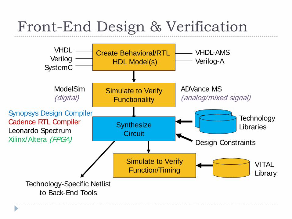
Front-End Design & Verification
Create Behavioral/RTL HDL Model(s)
Simulate to VerifyFunctionality
SynthesizeCircuit
Synopsys Design CompilerCadence RTL CompilerLeonardo SpectrumXilinx/Altera (FPGA)
ModelSim(digital)
VHDL-AMSVerilog-A
ADVance MS (analog/mixed signal)
VHDLVerilog
SystemC
Technology Libraries
Technology-Specific Netlistto Back-End Tools
Simulate to VerifyFunction/Timing
VITALLibrary
Design Constraints
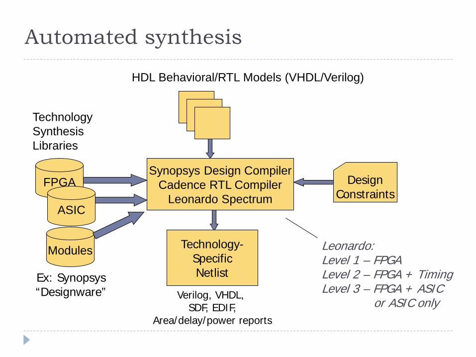
Automated synthesis
Synopsys Design CompilerCadence RTL Compiler
Leonardo Spectrum
HDL Behavioral/RTL Models (VHDL/Verilog)
FPGA
ASIC
TechnologySynthesis Libraries
Technology-SpecificNetlist
DesignConstraints
Verilog, VHDL, SDF, EDIF,
Area/delay/power reports
Leonardo:Level 1 – FPGALevel 2 – FPGA + TimingLevel 3 – FPGA + ASIC
or ASIC only
Modules
Ex: Synopsys“Designware”
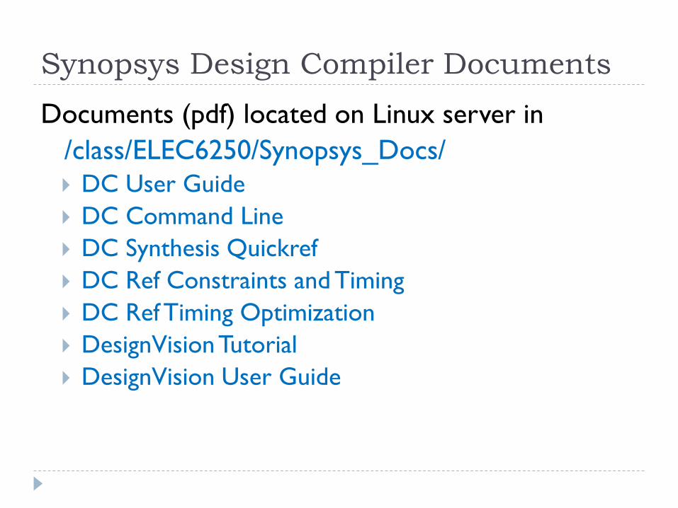
Synopsys Design Compiler DocumentsDocuments (pdf) located on Linux server in
/class/ELEC6250/Synopsys_Docs/ DC User Guide DC Command Line DC Synthesis Quickref DC Ref Constraints and Timing DC Ref Timing Optimization DesignVisionTutorial DesignVision User Guide
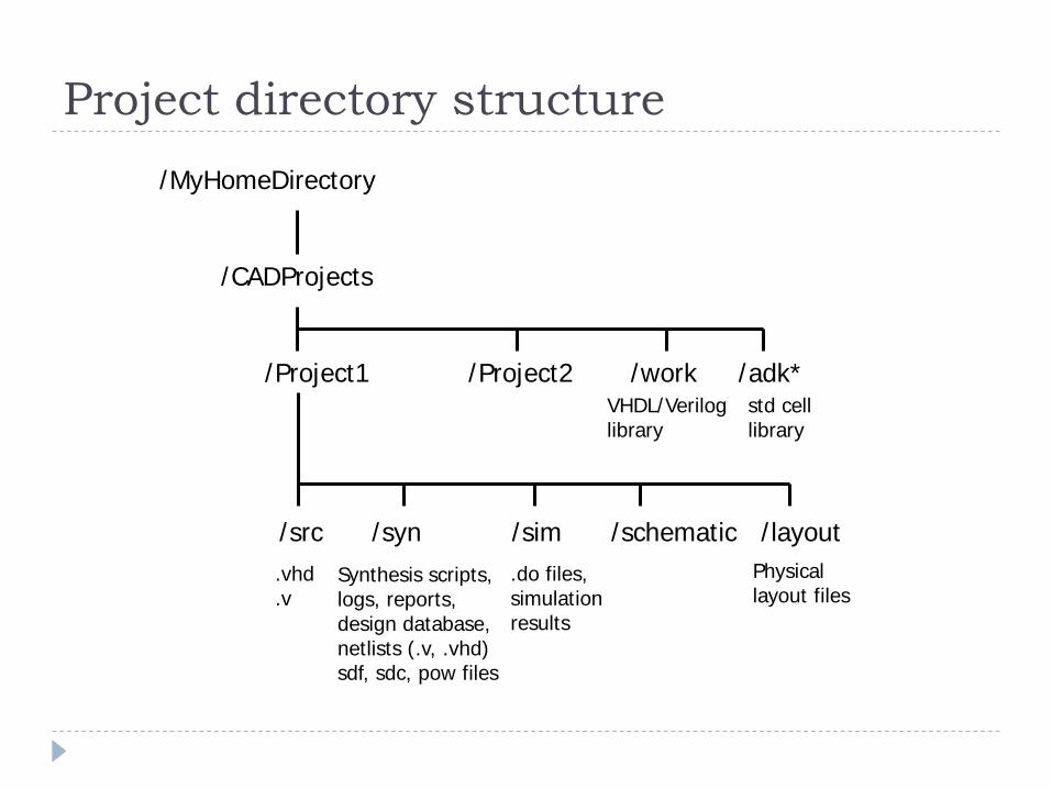
Project directory structure
/CADProjects
/MyHomeDirectory
/Project1 /Project2 /work /adk*
/src /syn /sim /schematic /layout
VHDL/Veriloglibrary
std celllibrary
.vhd
.vSynthesis scripts,logs, reports,design database,netlists (.v, .vhd)sdf, sdc, pow files
.do files,simulationresults
Physicallayout files
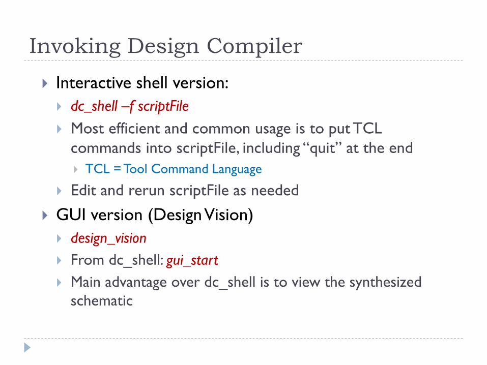
Invoking Design Compiler Interactive shell version: dc_shell –f scriptFile Most efficient and common usage is to put TCL
commands into scriptFile, including “quit” at the end TCL = Tool Command Language
Edit and rerun scriptFile as needed
GUI version (Design Vision) design_vision From dc_shell: gui_start Main advantage over dc_shell is to view the synthesized
schematic
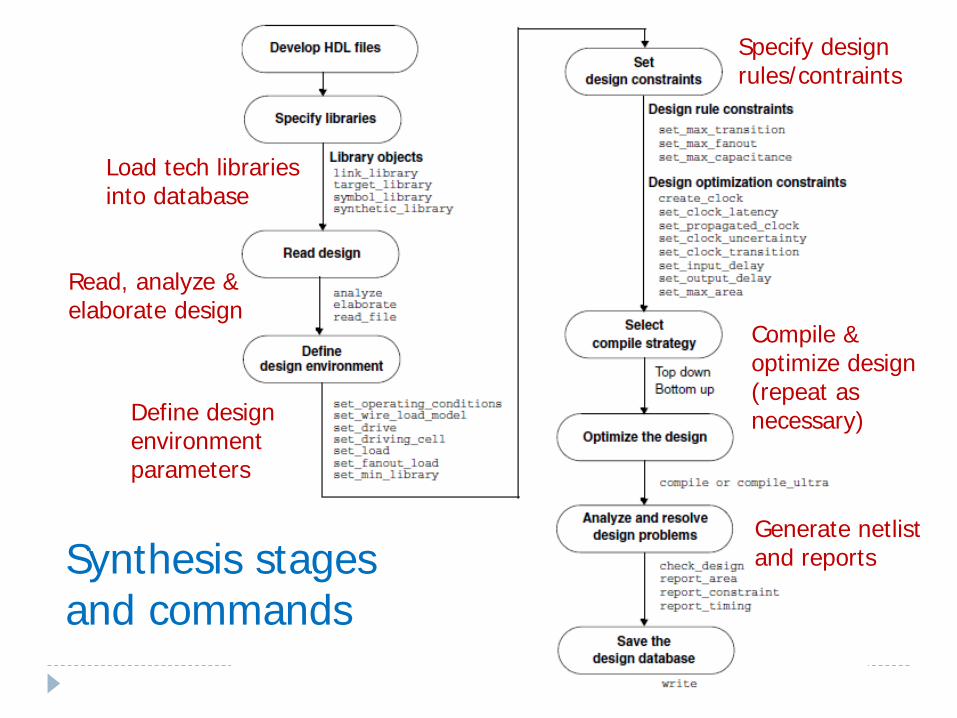
Synthesis stages and commands
Load tech librariesinto database
Read, analyze & elaborate design
Define designenvironmentparameters
Specify designrules/contraints
Compile & optimize design (repeat as necessary)
Generate netlist and reports
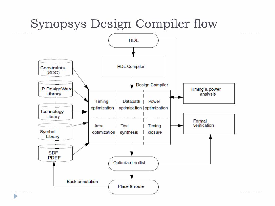
Synopsys Design Compiler flow
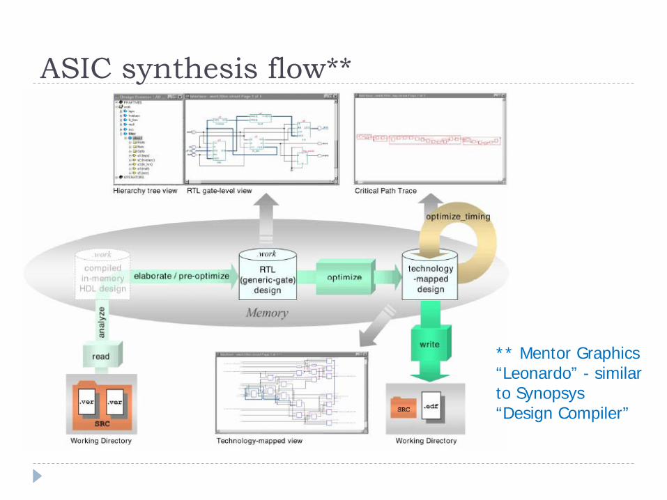
ASIC synthesis flow**
** Mentor Graphics “Leonardo” - similar to Synopsys “Design Compiler”
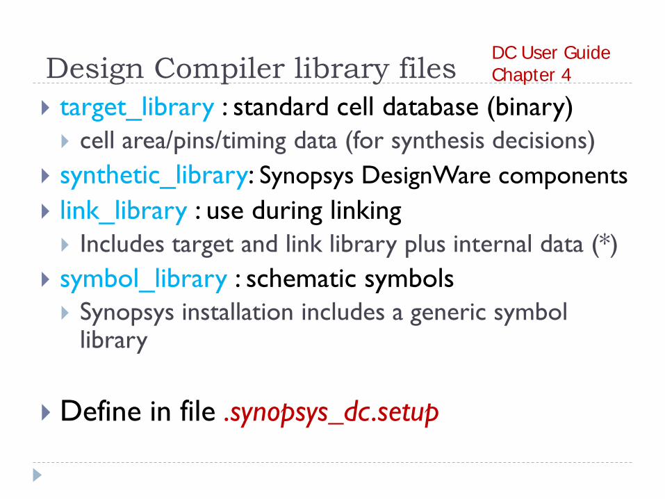
Design Compiler library files target_library : standard cell database (binary) cell area/pins/timing data (for synthesis decisions)
synthetic_library: Synopsys DesignWare components link_library : use during linking Includes target and link library plus internal data (*)
symbol_library : schematic symbols Synopsys installation includes a generic symbol
library
Define in file .synopsys_dc.setup
DC User GuideChapter 4
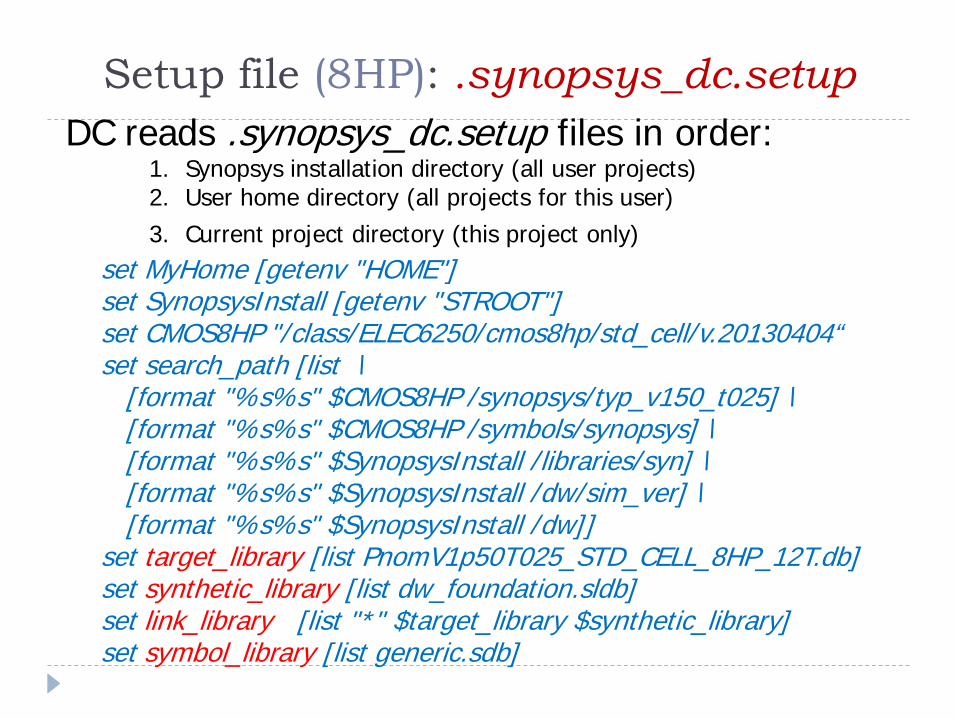
Setup file (8HP): .synopsys_dc.setup
set MyHome [getenv "HOME"]set SynopsysInstall [getenv "STROOT"]set CMOS8HP "/class/ELEC6250/cmos8hp/std_cell/v.20130404“set search_path [list \
[format "%s%s" $CMOS8HP /synopsys/typ_v150_t025] \[format "%s%s" $CMOS8HP /symbols/synopsys] \[format "%s%s" $SynopsysInstall /libraries/syn] \[format "%s%s" $SynopsysInstall /dw/sim_ver] \[format "%s%s" $SynopsysInstall /dw]]
set target_library [list PnomV1p50T025_STD_CELL_8HP_12T.db]set synthetic_library [list dw_foundation.sldb]set link_library [list "*" $target_library $synthetic_library]set symbol_library [list generic.sdb]
DC reads .synopsys_dc.setup files in order:1. Synopsys installation directory (all user projects)2. User home directory (all projects for this user)3. Current project directory (this project only)
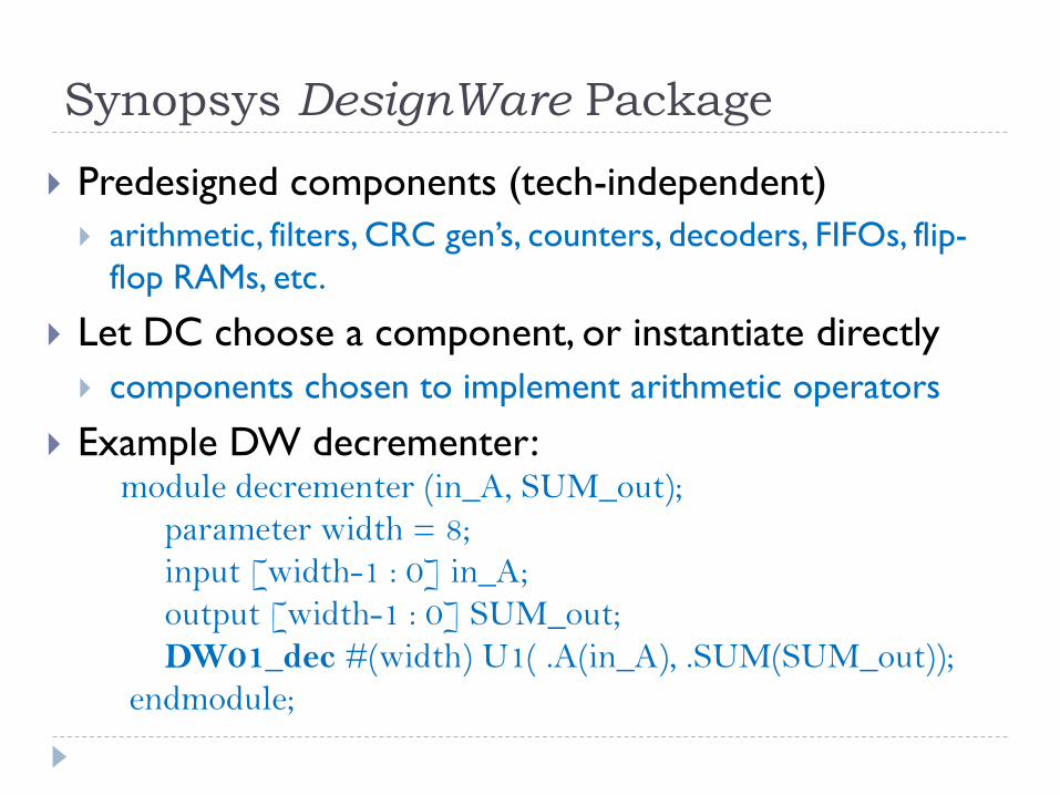
Synopsys DesignWare Package
Predesigned components (tech-independent) arithmetic, filters, CRC gen’s, counters, decoders, FIFOs, flip-
flop RAMs, etc.
Let DC choose a component, or instantiate directly components chosen to implement arithmetic operators
Example DW decrementer:module decrementer (in_A, SUM_out);
parameter width = 8;input [width-1 : 0] in_A;output [width-1 : 0] SUM_out;DW01_dec #(width) U1( .A(in_A), .SUM(SUM_out));
endmodule;
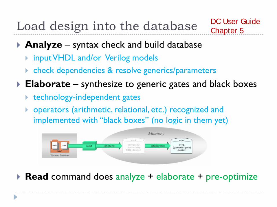
Load design into the database Analyze – syntax check and build database input VHDL and/or Verilog models check dependencies & resolve generics/parameters
Elaborate – synthesize to generic gates and black boxes technology-independent gates operators (arithmetic, relational, etc.) recognized and
implemented with “black boxes” (no logic in them yet)
Read command does analyze + elaborate + pre-optimize
DC User GuideChapter 5
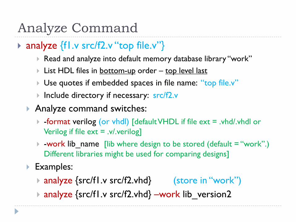
Analyze Command analyze {f1.v src/f2.v “top file.v”}
Read and analyze into default memory database library “work” List HDL files in bottom-up order – top level last Use quotes if embedded spaces in file name: “top file.v” Include directory if necessary: src/f2.v
Analyze command switches: -format verilog (or vhdl) [default VHDL if file ext = .vhd/.vhdl or
Verilog if file ext = .v/.verilog] -work lib_name [lib where design to be stored (default = “work”.)
Different libraries might be used for comparing designs]
Examples: analyze {src/f1.v src/f2.vhd} (store in “work”) analyze {src/f1.v src/f2.vhd} –work lib_version2
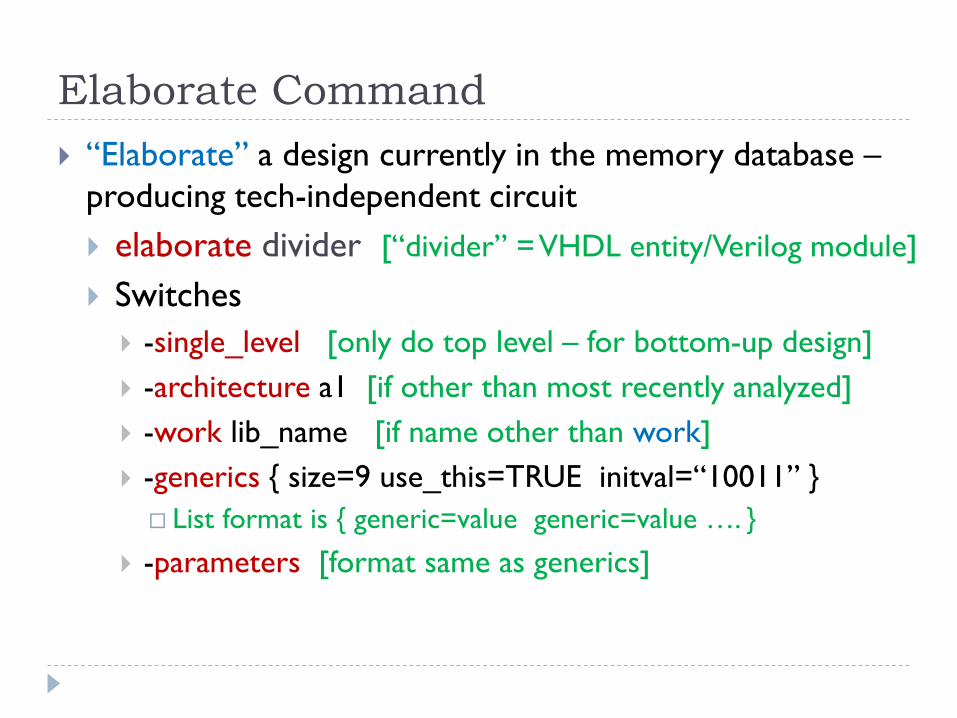
Elaborate Command “Elaborate” a design currently in the memory database –
producing tech-independent circuit elaborate divider [“divider” = VHDL entity/Verilog module]
Switches -single_level [only do top level – for bottom-up design] -architecture a1 [if other than most recently analyzed] -work lib_name [if name other than work] -generics { size=9 use_this=TRUE initval=“10011” } List format is { generic=value generic=value …. }
-parameters [format same as generics]
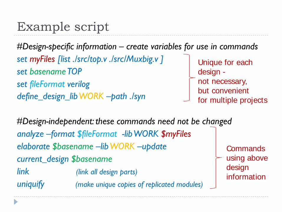
Example script#Design-specific information – create variables for use in commandsset myFiles [list ./src/top.v ./src/Muxbig.v ]set basenameTOPset fileFormat verilogdefine_design_libWORK –path ./syn
#Design-independent: these commands need not be changedanalyze –format $fileFormat -lib WORK $myFileselaborate $basename –lib WORK –updatecurrent_design $basenamelink (link all design parts)
uniquify (make unique copies of replicated modules)
Unique for each design -not necessary,but convenientfor multiple projects
Commandsusing abovedesigninformation
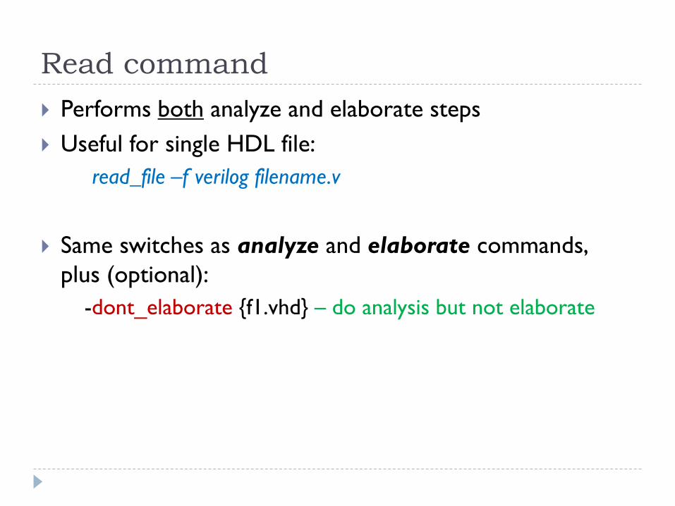
Read command Performs both analyze and elaborate steps Useful for single HDL file:
read_file –f verilog filename.v
Same switches as analyze and elaborate commands, plus (optional):
-dont_elaborate {f1.vhd} – do analysis but not elaborate
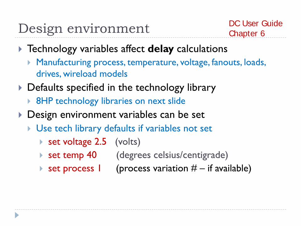
Design environment Technology variables affect delay calculations Manufacturing process, temperature, voltage, fanouts, loads,
drives, wireload models Defaults specified in the technology library 8HP technology libraries on next slide
Design environment variables can be set Use tech library defaults if variables not set
set voltage 2.5 (volts) set temp 40 (degrees celsius/centigrade) set process 1 (process variation # – if available)
DC User GuideChapter 6
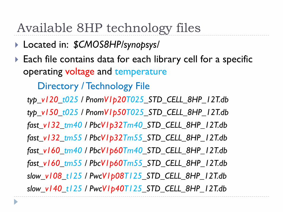
Available 8HP technology files Located in: $CMOS8HP/synopsys/ Each file contains data for each library cell for a specific
operating voltage and temperatureDirectory / Technology File
typ_v120_t025 / PnomV1p20T025_STD_CELL_8HP_12T.dbtyp_v150_t025 / PnomV1p50T025_STD_CELL_8HP_12T.dbfast_v132_tm40 / PbcV1p32Tm40_STD_CELL_8HP_12T.dbfast_v132_tm55 / PbcV1p32Tm55_STD_CELL_8HP_12T.dbfast_v160_tm40 / PbcV1p60Tm40_STD_CELL_8HP_12T.dbfast_v160_tm55 / PbcV1p60Tm55_STD_CELL_8HP_12T.dbslow_v108_t125 / PwcV1p08T125_STD_CELL_8HP_12T.dbslow_v140_t125 / PwcV1p40T125_STD_CELL_8HP_12T.db
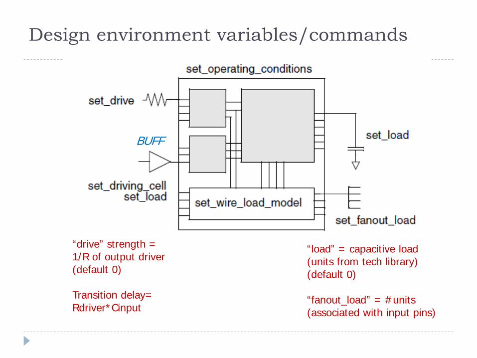
Design environment variables/commands
BUFF
“drive” strength =1/R of output driver(default 0)
Transition delay=Rdriver*Cinput
“load” = capacitive load(units from tech library)(default 0)
“fanout_load” = #units(associated with input pins)
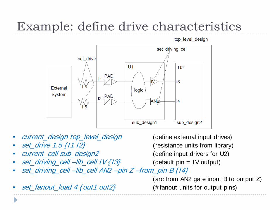
Example: define drive characteristics
• current_design top_level_design (define external input drives)• set_drive 1.5 {I1 I2} (resistance units from library)• current_cell sub_design2 (define input drivers for U2)• set_driving_cell –lib_cell IV {I3} (default pin = IV output)• set_driving_cell –lib_cell AN2 –pin Z –from_pin B {I4}
(arc from AN2 gate input B to output Z)• set_fanout_load 4 {out1 out2} (#fanout units for output pins)
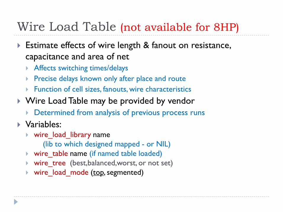
Wire Load Table (not available for 8HP) Estimate effects of wire length & fanout on resistance,
capacitance and area of net Affects switching times/delays Precise delays known only after place and route Function of cell sizes, fanouts, wire characteristics
Wire Load Table may be provided by vendor Determined from analysis of previous process runs
Variables: wire_load_library name
(lib to which designed mapped - or NIL) wire_table name (if named table loaded) wire_tree (best,balanced,worst, or not set) wire_load_mode (top, segmented)

Setting design constraints Design rule constraints: rules from library vendor for
proper functioning of the fabricated circuit Must not be violated Common constraints: transition time, fanout load, capacitance
Design optimization constraints: user-specified timing and area optimization goals DC tries to optimize these without violating design rules Common constraints: timing and area
DC User GuideChapter 7
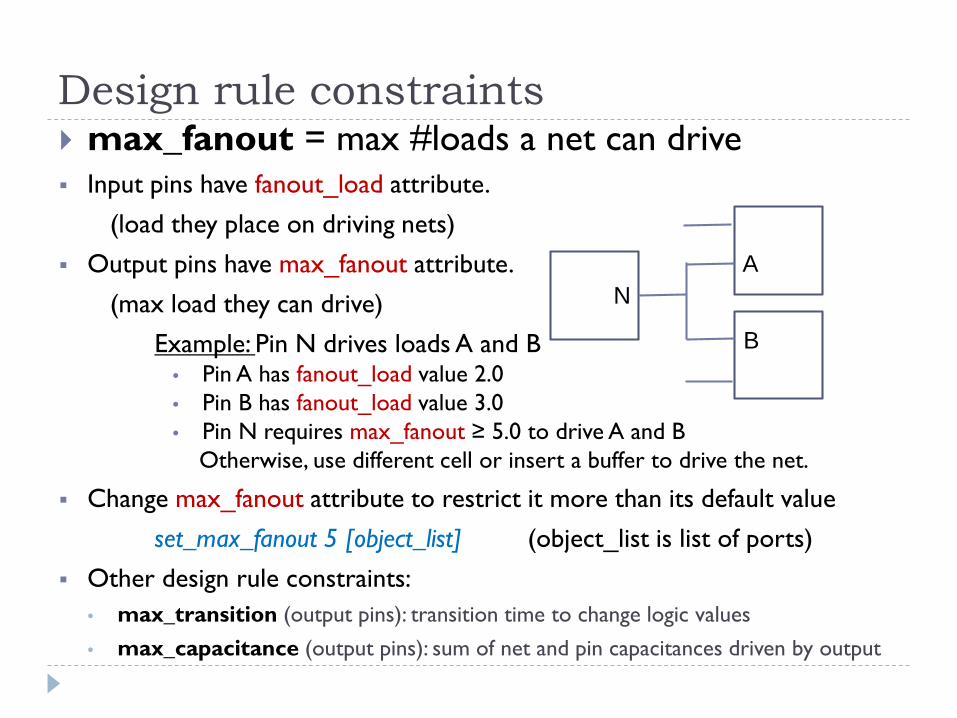
Design rule constraints max_fanout = max #loads a net can drive Input pins have fanout_load attribute.
(load they place on driving nets) Output pins have max_fanout attribute.
(max load they can drive)Example: Pin N drives loads A and B
• Pin A has fanout_load value 2.0• Pin B has fanout_load value 3.0• Pin N requires max_fanout ≥ 5.0 to drive A and B
Otherwise, use different cell or insert a buffer to drive the net.
Change max_fanout attribute to restrict it more than its default valueset_max_fanout 5 [object_list] (object_list is list of ports)
Other design rule constraints:• max_transition (output pins): transition time to change logic values• max_capacitance (output pins): sum of net and pin capacitances driven by output
NA
B
Design optimization constraints Speed path delays (min,max) clock specifications (period/frequency/duty)
Area speed is primary goal optimize area if timing constraints met target area 0 forces small as possible set_max_area 2000
Choose realistic constraints (within 1-10%) avoid extra buffers/gates on loaded nets
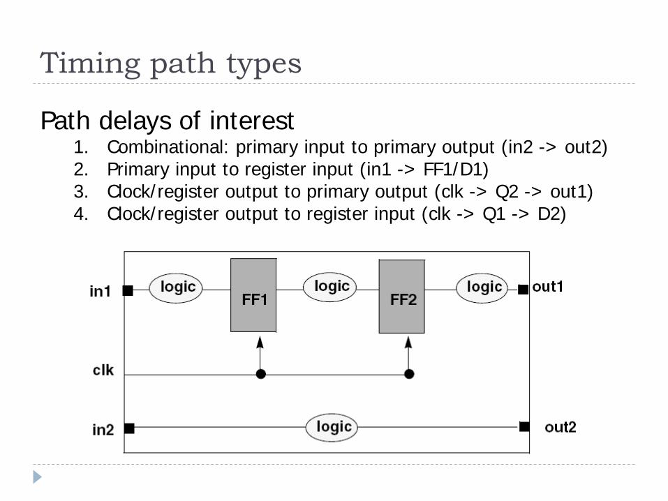
Timing path types
Path delays of interest1. Combinational: primary input to primary output (in2 -> out2)2. Primary input to register input (in1 -> FF1/D1)3. Clock/register output to primary output (clk -> Q2 -> out1) 4. Clock/register output to register input (clk -> Q1 -> D2)
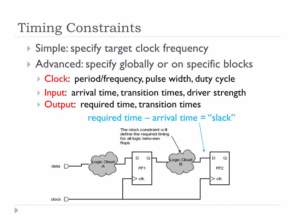
Timing Constraints Simple: specify target clock frequency Advanced: specify globally or on specific blocks Clock: period/frequency, pulse width, duty cycle Input: arrival time, transition times, driver strength Output: required time, transition times
required time – arrival time = “slack”
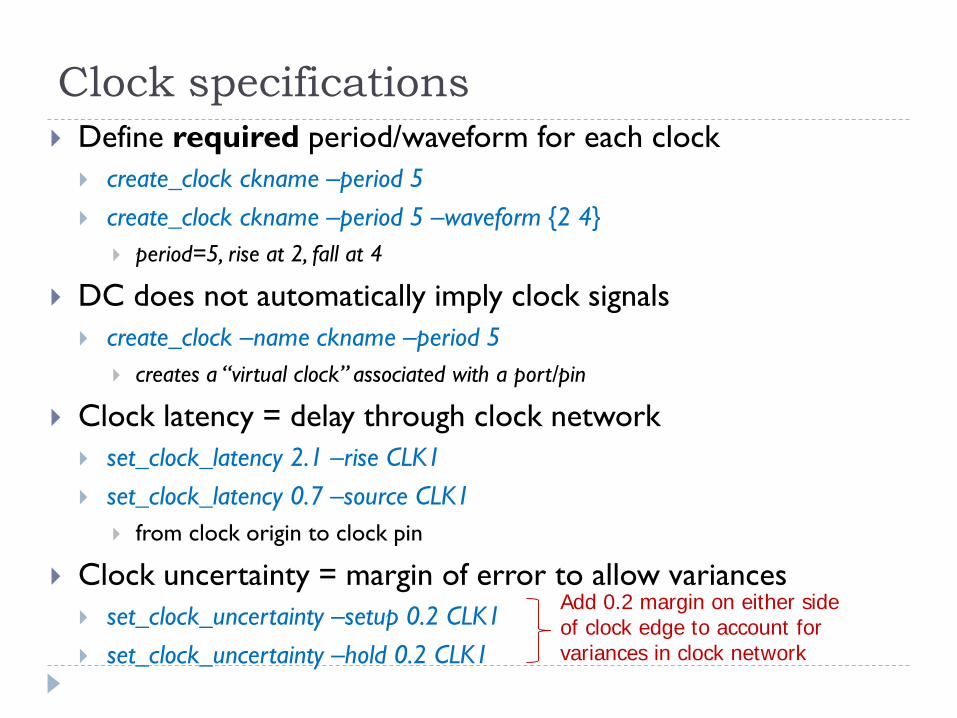
Clock specifications Define required period/waveform for each clock create_clock ckname –period 5 create_clock ckname –period 5 –waveform {2 4}
period=5, rise at 2, fall at 4
DC does not automatically imply clock signals create_clock –name ckname –period 5
creates a “virtual clock” associated with a port/pin
Clock latency = delay through clock network set_clock_latency 2.1 –rise CLK1 set_clock_latency 0.7 –source CLK1
from clock origin to clock pin
Clock uncertainty = margin of error to allow variances set_clock_uncertainty –setup 0.2 CLK1 set_clock_uncertainty –hold 0.2 CLK1
Add 0.2 margin on either side of clock edge to account forvariances in clock network
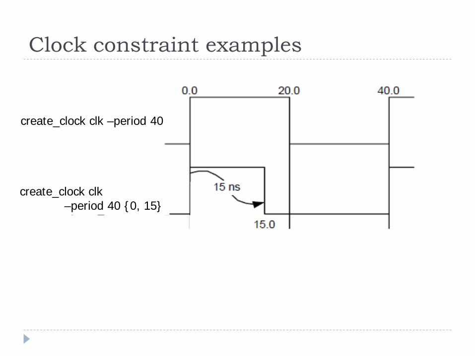
Clock constraint examples
create_clock clk –period 40
create_clock clk–period 40 {0, 15}
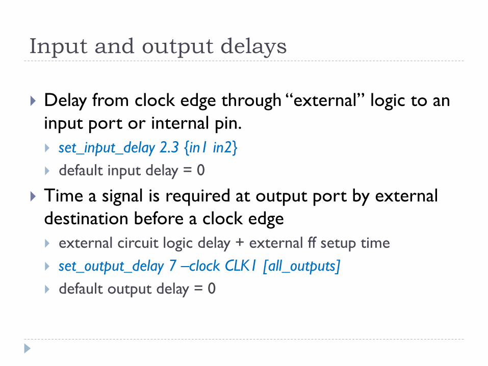
Input and output delays
Delay from clock edge through “external” logic to an input port or internal pin. set_input_delay 2.3 {in1 in2} default input delay = 0
Time a signal is required at output port by external destination before a clock edge external circuit logic delay + external ff setup time set_output_delay 7 –clock CLK1 [all_outputs] default output delay = 0
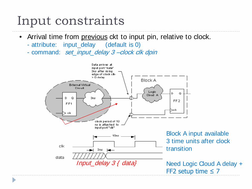
• Arrival time from previous ckt to input pin, relative to clock.- attribute: input_delay (default is 0)- command: set_input_delay 3 –clock clk dpin
Input_delay 3 { data}
Input constraints
Block A input available3 time units after clock transition
Need Logic Cloud A delay + FF2 setup time ≤ 7
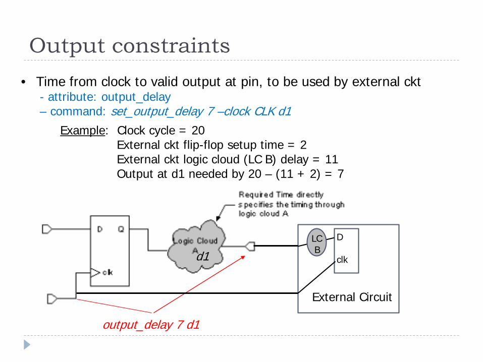
• Time from clock to valid output at pin, to be used by external ckt- attribute: output_delay– command: set_output_delay 7 –clock CLK d1
output_delay 7 d1
d1
Output constraints
External Circuit
Example: Clock cycle = 20External ckt flip-flop setup time = 2External ckt logic cloud (LC B) delay = 11 Output at d1 needed by 20 – (11 + 2) = 7
D
clk
LC B
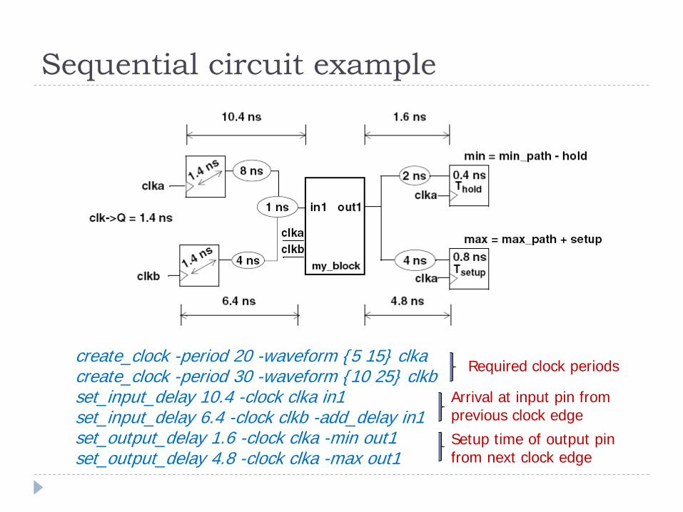
Sequential circuit example
create_clock -period 20 -waveform {5 15} clkacreate_clock -period 30 -waveform {10 25} clkbset_input_delay 10.4 -clock clka in1set_input_delay 6.4 -clock clkb -add_delay in1set_output_delay 1.6 -clock clka -min out1set_output_delay 4.8 -clock clka -max out1
Arrival at input pin from previous clock edgeSetup time of output pinfrom next clock edge
Required clock periods
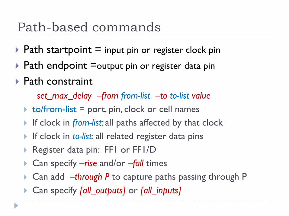
Path-based commands
Path startpoint = input pin or register clock pin
Path endpoint =output pin or register data pin
Path constraintset_max_delay –from from-list –to to-list value
to/from-list = port, pin, clock or cell names If clock in from-list: all paths affected by that clock If clock in to-list: all related register data pins Register data pin: FF1 or FF1/D Can specify –rise and/or –fall times Can add –through P to capture paths passing through P Can specify [all_outputs] or [all_inputs]
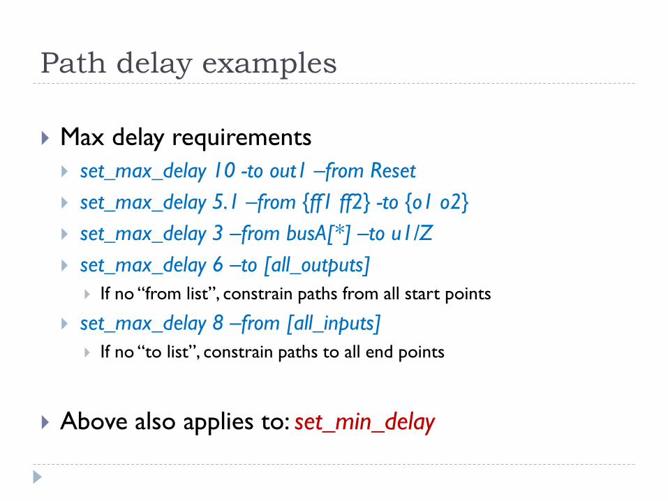
Path delay examples
Max delay requirements set_max_delay 10 -to out1 –from Reset set_max_delay 5.1 –from {ff1 ff2} -to {o1 o2} set_max_delay 3 –from busA[*] –to u1/Z set_max_delay 6 –to [all_outputs]
If no “from list”, constrain paths from all start points
set_max_delay 8 –from [all_inputs] If no “to list”, constrain paths to all end points
Above also applies to: set_min_delay
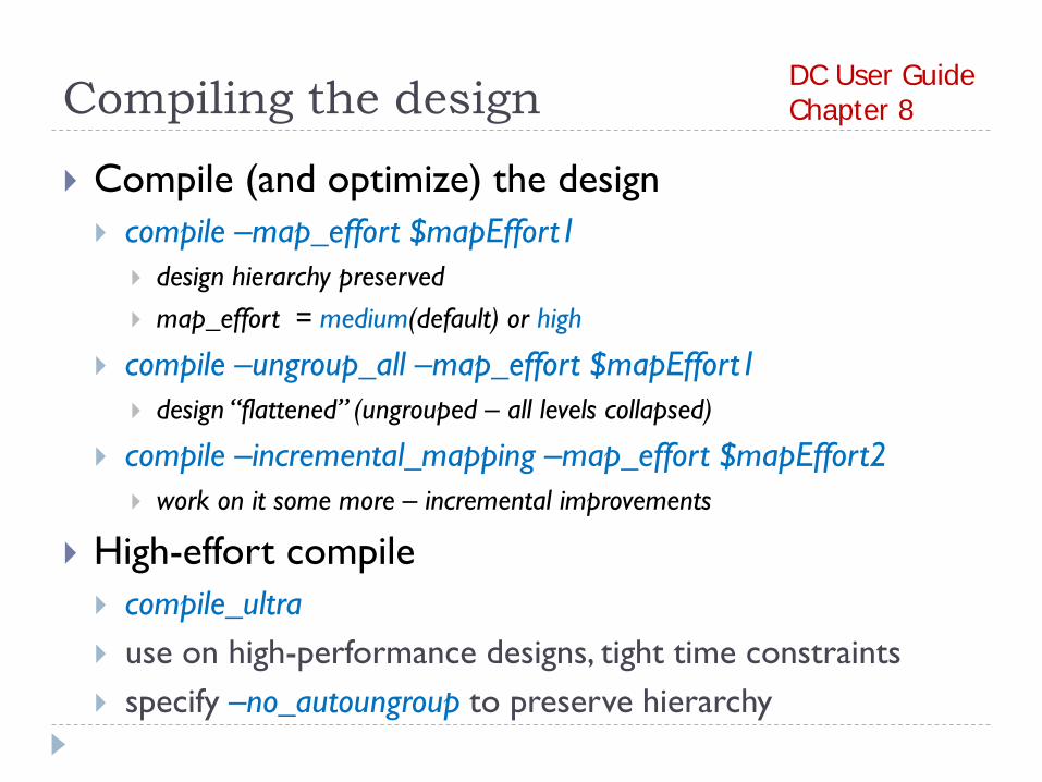
Compiling the design
Compile (and optimize) the design compile –map_effort $mapEffort1
design hierarchy preserved map_effort = medium(default) or high
compile –ungroup_all –map_effort $mapEffort1 design “flattened” (ungrouped – all levels collapsed)
compile –incremental_mapping –map_effort $mapEffort2 work on it some more – incremental improvements
High-effort compile compile_ultra use on high-performance designs, tight time constraints specify –no_autoungroup to preserve hierarchy
DC User GuideChapter 8
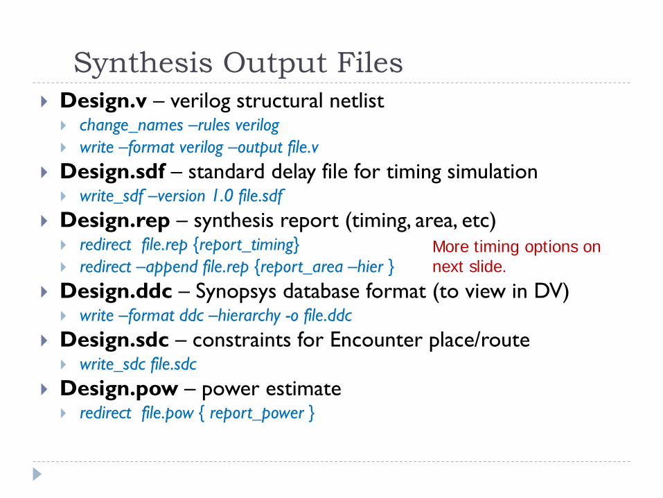
Synthesis Output Files Design.v – verilog structural netlist change_names –rules verilog write –format verilog –output file.v
Design.sdf – standard delay file for timing simulation write_sdf –version 1.0 file.sdf
Design.rep – synthesis report (timing, area, etc) redirect file.rep {report_timing} redirect –append file.rep {report_area –hier }
Design.ddc – Synopsys database format (to view in DV) write –format ddc –hierarchy -o file.ddc
Design.sdc – constraints for Encounter place/route write_sdc file.sdc
Design.pow – power estimate redirect file.pow { report_power }
More timing options onnext slide.
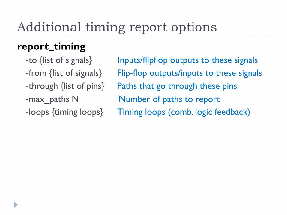
Additional timing report optionsreport_timing
-to {list of signals} Inputs/flipflop outputs to these signals-from {list of signals} Flip-flop outputs/inputs to these signals-through {list of pins} Paths that go through these pins-max_paths N Number of paths to report-loops {timing loops} Timing loops (comb. logic feedback)
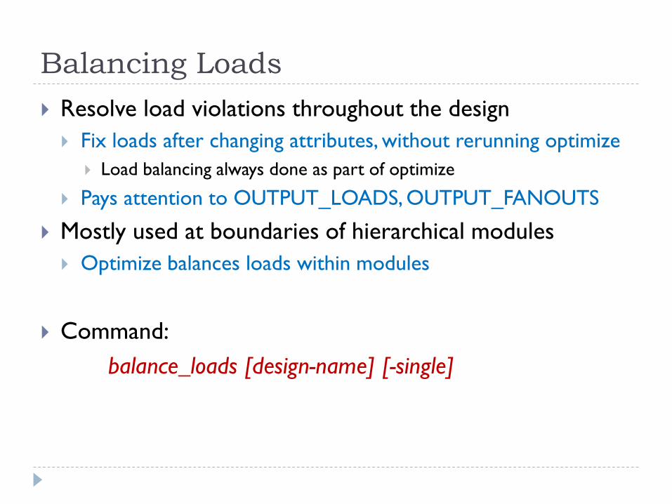
Balancing Loads Resolve load violations throughout the design Fix loads after changing attributes, without rerunning optimize
Load balancing always done as part of optimize
Pays attention to OUTPUT_LOADS, OUTPUT_FANOUTS
Mostly used at boundaries of hierarchical modules Optimize balances loads within modules
Command:balance_loads [design-name] [-single]
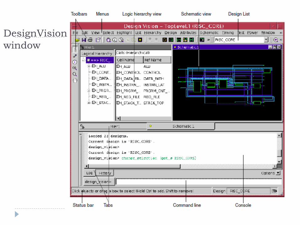
DesignVisionwindow
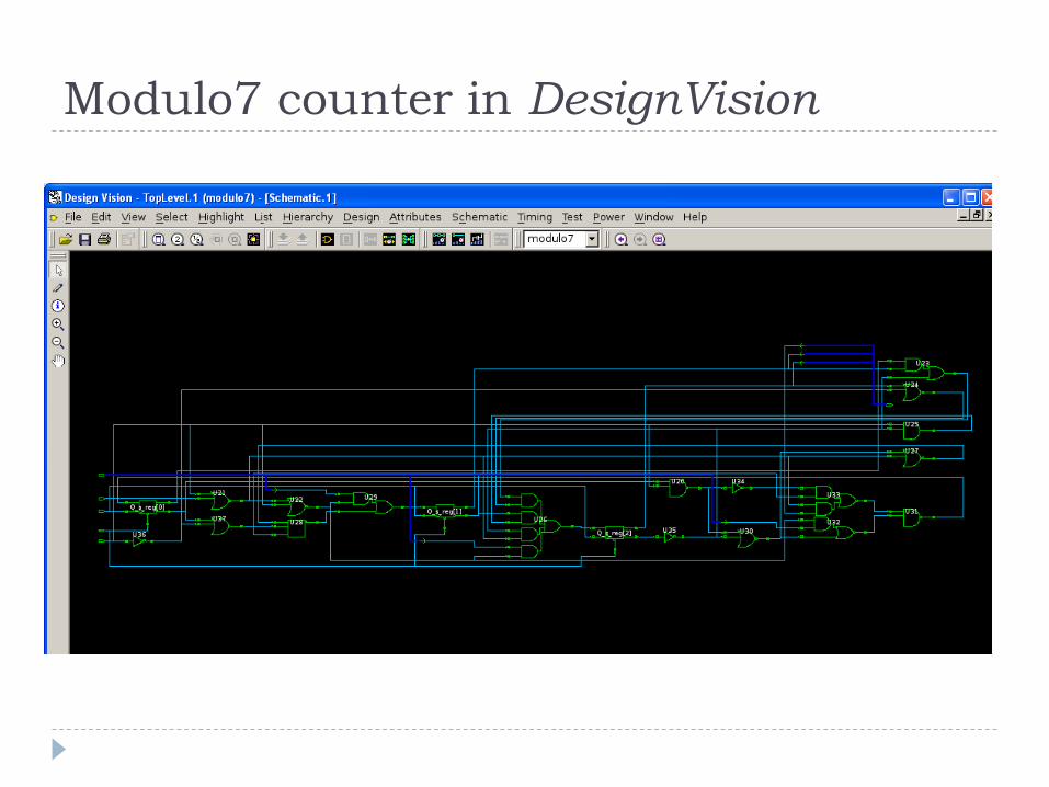
Modulo7 counter in DesignVision