atwilc1000b-mut ieee® 802.11 b/g/n link controller...
TRANSCRIPT
ATWILC1000B-MUT ATWILC1000B-MUT IEEEreg 80211 bgn Link Controller
SoC
Introduction
The ATWILC1000B is a single chip IEEEreg 80211 bgn RadioBasebandMAC link controller optimized forlow-power mobile applications The ATWILC1000B supports single stream 1x1 80211n mode providingup to 72 Mbps PHY rate The ATWILC1000B features a fully integrated Power Amplifier (PA) Low NoiseAmplifier (LNA) Switch and Power Management The ATWILC1000B offers very low-power consumptionwhile simultaneously providing high performance and minimal bill of materials
The ATWILC1000B provides multiple peripheral interfaces including Universal Asynchronous ReceiverTransmitter (UART) Serial Peripheral Interface (SPI) Inter-Integrated Circuit (I2C) and Secure DigitalInput Output (SDIO) The clock source for the ATWILC1000B is provided by an external crystal at 26MHz The ATWILC1000B is available in both QFN and Wafer Level Chip Scale Package (WLCSP)packaging
Features
bull IEEE 8021 bgn 20 MHz (1x1) Solutionbull Single Spatial Stream in 24 GHz ISM Bandbull Integrated PA and TR Switchbull Superior Sensitivity and Range via Advanced PHY Signal Processingbull Advanced Equalization and Channel Estimationbull Advanced Carrier and Timing Synchronizationbull Wi-Fi Directreg and Soft-AP Supportbull Supports IEEE 80211 WEP WPA WPA2 Securitybull Superior MAC Throughput via Hardware Accelerated Two-Level A-MSDUA-MPDU Frame
Aggregation and Block Acknowledgmentbull On-Chip Memory Management Engine to Reduce Host Loadbull SPI SDIO and I2C Host Interfacesbull Operating Temperature Ranges from -40degC to +85degCbull Power Save Modes
ndash lt1 μA Deep Power-Down mode typical at 33V IOndash 280 μA Doze mode with chip settings preserved (used for beacon monitoring)ndash On-chip low-power sleep oscillatorndash Fast host wake up from Doze mode by a pin or host IO transaction
copy 2018 Microchip Technology Inc Datasheet DS70005386A-page 1
Table of Contents
Introduction1
Features 1
1 Ordering Information and IC Marking 4
2 Block Diagram 5
3 Pinout and Package Information 631 Pin Description 632 Package Description 13
4 Electrical Specifications1541 Absolute Ratings 1542 Recommended Operating Conditions 1543 DC Electrical Characteristics16
5 Clocking1751 Crystal Oscillator 1752 Low-Power Oscillator 18
6 CPU and Memory Subsystem 1961 Processor 1962 Memory Subsystem1963 Nonvolatile Memory (eFuse) 19
7 WLAN Subsystem 2171 MAC 2172 PHY2273 Radio22
8 External Interfaces2781 I2C Slave Interface 2782 I2C Master Interface 2883 SPI Slave Interface2984 SPI Master Interface3185 SDIO Slave Interface3386 UART Debug Interface 3487 GPIOs35
9 Power Management 3691 Power Architecture3692 Power Consumption3793 Power-UpDown Sequence3994 Digital IO Pin Behavior During Power-up Sequences 40
ATWILC1000B-MUT
copy 2018 Microchip Technology Inc Datasheet DS70005386A-page 2
10 Reference Design41
11 Reflow Profile Information 42111 Storage Condition42112 Solder Paste42113 Stencil Design 42114 Printing Process 42115 Baking Conditions 42116 Soldering and Reflow Condition43
12 Reference Documentation and Support 45
13 Document Revision History 46
The Microchip Web Site 47
Customer Change Notification Service47
Customer Support 47
Microchip Devices Code Protection Feature 47
Legal Notice48
Trademarks 48
Quality Management System Certified by DNV49
Worldwide Sales and Service50
ATWILC1000B-MUT
copy 2018 Microchip Technology Inc Datasheet DS70005386A-page 3
1 Ordering Information and IC MarkingThe following table provides the ordering details of the ATWILC1000B IC
Table 1-1 Ordering Details
Ordering Code(1) Package Type IC Marking
ATWILC1000B-MU-ABCD 5 x 5 QFN in Tape and Reel ATWILC1000B
ATWILC1000B-UU-ABCD 324 x 324 mm WLCSP in Tapeand Reel
ATWILC1000B
Note 1 ABCD interprets as
A can be Y indicating Tray or T indicating Tape and Reel
BCD equals to 042 for part assigned with MAC ID and blank for part with no MAC ID
The following table lists possible combinations for ordering the ATWILC1000B-MU andATWILC1000B-UU
Ordering Code Description
ATWILC1000B-MU-T No MAC ID and ship in Tape and Reel
ATWILC1000B-MU-Y No MAC ID and ship in Tray
ATWILC1000B-MU-Y042 MAC ID assigned and ship in Tray
ATWILC1000B-MU-T042 MAC ID assigned and ship in Tape and Reel
ATWILC1000B-UU-T No MAC ID and ship in Tape and Reel
ATWILC1000B-UU-Y No MAC ID and ship in Tray
ATWILC1000B-UU-Y042 MAC ID assigned and ship in Tray
ATWILC1000B-UU-T042 MAC ID assigned and ship in Tape and Reel
ATWILC1000B-MUTOrdering Information and IC Marking
copy 2018 Microchip Technology Inc Datasheet DS70005386A-page 4
2 Block DiagramThe following figure provides a basic overview of the ATWILC1000B IC
Figure 2-1 ATWILC1000B Block Diagram
X
X
TxDigital Core
DPD
80211bgniFFT
80211bgnCoding
Host Interface
Microcontroller
DAC
ADCRxDigital Core
80211bgnOFDM
Channel Estimation Equalization
80211bgn Forward
ErrorCorrection
RAM
PLL80211bgn
MAC ~
SDIO SPI Bluetooth Coexistance
XOPMURTC Clock
Vbatt
UART GPIOI2C
ATWILC1000B
ATWILC1000B-MUTBlock Diagram
copy 2018 Microchip Technology Inc Datasheet DS70005386A-page 5
3 Pinout and Package Information
31 Pin DescriptionThe ATWILC1000B is offered in an exposed pad 40-pin QFN package This package has an exposedpaddle that must be connected to the system board ground The QFN package pin assignment and theWLCSP package pin assignment are shown in the following figures The color shading is used to indicatethe pin type as follows
bull Green ndash powerbull Red ndash analogbull Blue ndash digital IObull Yellow ndash digital inputbull Grey ndash unconnected or reserved
Figure 3-1 Pin Assignment
12
TP_P
VDD_RF_RX
VDD_AMS
VDD_RF_TX
VDD_BATT_PPA
VDD_BATT_PA
RFIOP
RFION
SDIO_SPI_CFG
GPIO0HOST_WAKEUP
GPI
O2
IRQ
N
SD_D
AT3
SD_D
AT2
SPI_
RXD
VDD
C
VDD
IO
SD_D
AT1
SPI_
SSN
SD_D
AT0
SPI_
TXD
SD_C
MD
SPI
_SC
K
SD_CLK
VBAT
T_BU
CK
GPIO5
GPIO4
GPIO3
VDDC
VDDIO
TEST_MODE
GPIO1RTC_CLK
CHIP_EN
VREG_BUCK
VSW
TP_N
VDD
IO_A
VDD
_VC
O
VDD
_SXD
IG
XO_P
XO_N
RES
ETN
I2C
_SD
A
I2C
_SC
L
GPI
O6
11 13 14 15 16 17 18 19 20
21
2
1
3
4
5
6
7
8
9
10
23
24
25
26
27
28
29
30
22
323334353637383940 31
ATWILC1000B
PADDLE VSS41
ATWILC1000B-MUTPinout and Package Information
copy 2018 Microchip Technology Inc Datasheet DS70005386A-page 6
Figure 3-2 WLCSP Package Pin Assignment
7 6 5 4 3 2 1
A
B
C
D
E
F
G
H
8
GND_SXDIGVDDIO_A VDD_
SXDIG XO_N RESETN I2C_SCL GPIO6
GND_IOVDD_RF TP_N XO_P I2C_SDA GPIO5 GPIO16NC
GPIO13GND_RF_RX TP_P GPIO18 GPIO17 GPIO15 VDDC
VDD_BATT GPIO4 TEST_
MODE VDDIOGND_BATT_
PPA
GND_BATT_PA GPIO3 GPIO1
RTC_CLK VSS
GPIO2 IRQN
GND_AMS
GPIO0 HOST_
WAKEUPSD_DAT3 VREG_
BUCK CHIP_EN GND_BIASTX_P
SD_DAT2 SPI_RXD
SDIO_SPI_CFG GPIO12 SD_DAT1
SPI_SSNSD_DAT0SPI_TXD SD_CLK GND_
BUCKTX_N
VDDIOGPIO11 VDDC VSS SD_CMD SPI_SCK
VBATT_BUCK VSWVDD_
AMS
The ATWILC1000B pins are described in the following table
Table 3-1 Pin Description
QFN Pin Number WLCSP PinNumber Pin Name Pin Type Description
1 C6 TP_P Analog Test PinNoConnect
2 B7 VDD_RF_RX Power Tuner RF Supply(see Section 91 PowerArchitecture)
ATWILC1000B-MUTPinout and Package Information
copy 2018 Microchip Technology Inc Datasheet DS70005386A-page 7
continued
QFN Pin Number WLCSP PinNumber Pin Name Pin Type Description
3 H8 VDD_AMS Power Tuner BB Supply(see Section 91 PowerArchitecture)
4 - VDD_RF_TX Power Tuner RF Supply(see Section 91 PowerArchitecture)
5 - VDD_BATT_PPA Power PA 1ST StageSupply (seeSection 91 PowerArchitecture)
6 D7 VDD_BATT_PA Power PA 2ND StageSupply (seeSection 91 PowerArchitecture)
7 - RFIOP Analog Positive RFDifferential IO (see Table 9-4)
8 - RFION Analog Negative RFDifferential IO (see Table 9-4)
9 G7 SDIO_SPI_CFG Digital Input Tie to 1 for SPI 0for SDIO
10 F6 GPIO0HOST_WAKE
Digital IOProgrammablePull-up
GPIO0SLEEPMode Control
11 F5 GPIO2IRQN Digital IOProgrammablePull-up
GPIO2DeviceInterrupt
12 F4 SD_DAT3 Digital IOProgrammablePull-up
SDIO Data3
13 G5 SD_DAT2SPI_RXD
Digital IOProgrammablePull-up
SDIO Data2SPIData RX
14 C1 VDDC Power Digital Core PowerSupply (seeSection 91 PowerArchitecture)
ATWILC1000B-MUTPinout and Package Information
copy 2018 Microchip Technology Inc Datasheet DS70005386A-page 8
continued
QFN Pin Number WLCSP PinNumber Pin Name Pin Type Description
15 D1 VDDIO Power Digital IO PowerSupply (seeSection 91 PowerArchitecture)
16 G4 SD_DAT1SPI_SSN
Digital IOProgrammablePull-up
SDIO Data1SPISlave Select
17 G3 SD_DAT0SPI_TXD
Digital IOProgrammablePull-up
SDIO Data0SPIData TX
18 H3 SD_CMDSPI_SCK
Digital IOProgrammablePull-up
SDIOCommandSPIClock
19 G2 SD_CLK Digital IOProgrammablePull-up
SDIO Clock
20 H2 VBATT_BUCK Power Battery Supply forDCDC Converter(see Section 91 PowerArchitecture)
21 H1 VSW Power Switching output ofDCDC Converter(see Section 91 PowerArchitecture)
22 F3 VREG_BUCK Power Core Power fromDCDC Converter(see Section 91 PowerArchitecture)
23 F2 CHIP_EN Analog PMU Enable
24 E2 GPIO1RTC_CLK Digital IOProgrammablePull-up
GPIO132kHzClock Input
25 D2 TEST_MODE Digital Input Test Mode ndash Usermust tie this pin toGND
ATWILC1000B-MUTPinout and Package Information
copy 2018 Microchip Technology Inc Datasheet DS70005386A-page 9
continued
QFN Pin Number WLCSP PinNumber Pin Name Pin Type Description
26 H5 VDDIO Power Digital IO PowerSupply (seeSection 91 PowerArchitecture)
27 H6 VDDC Power Digital Core PowerSupply (seeSection 91 PowerArchitecture)
28 E3 GPIO3 Digital IOProgrammablePull-up
GPIO3SPI_SCK_Flash
29 D3 GPIO4 Digital IOProgrammablePull-up
GPIO4SPI_SSN_Flash
30 B2 GPIO5 Digital IOProgrammablePull-up
GPIO5SPI_TXD_Flash
31 A1 GPIO6 Digital IOProgrammablePull-up
GPIO6SPI_RXD_Flash
32 A2 I2C_SCL Digital IOProgrammablePull-up
I2C Slave Clock(high-drive padsee Table 4-3)
33 B3 I2C_SDA Digital IOProgrammablePull-up
I2C Slave Data(high-drive padsee Table 4-3)
34 A3 RESETN Digital Input Active-Low HardReset
35 A4 XO_N Analog Crystal Oscillator N
36 B4 XO_P Analog Crystal Oscillator P
37 A6 VDD_SXDIG Power SX Power Supply(see Section 91 PowerArchitecture)
38 - VDD_VCO Power VCO Power Supply(see Section 91 PowerArchitecture)
ATWILC1000B-MUTPinout and Package Information
copy 2018 Microchip Technology Inc Datasheet DS70005386A-page 10
continued
QFN Pin Number WLCSP PinNumber Pin Name Pin Type Description
39 A7 VDDIO_A Power Tuner VDDIOPower Supply (seeSection 91 PowerArchitecture)
40 B6 TP_N Analog Test PinNoConnect
41(1) - PADDLE VSS Ground Connect to SystemBoard Ground
- A5 GND_SXDIG Ground SX GroundConnect to SystemBoard Ground
- B1 GPIO16 Digital IOProgrammablePull-up
GPIO16
- B5 GND_IO Ground IO GroundConnect to SystemBoard Ground
- B8 NC None ReservedNoConnect
- C2 GPIO15 Digital IOProgrammablePull-up
GPIO15
- C3 GPIO17 Digital IOProgrammablePull-up
GPIO17
- C4 GPIO18 Digital IOProgrammablePull-up
GPIO18
- C5 GPIO13 Digital IOProgrammablePull-up
GPIO13
- C7 GND_RF_RX Ground RF Rx GroundConnect to SystemBoard Ground
- D8 GND_BATT_PPA Ground PA 2nd StageGround Connectto System BoardGround
ATWILC1000B-MUTPinout and Package Information
copy 2018 Microchip Technology Inc Datasheet DS70005386A-page 11
continued
QFN Pin Number WLCSP PinNumber Pin Name Pin Type Description
- E1 VSS Ground Connect to SystemBoard Ground
- E7 GND_BATT_PA Ground PA 1st StageGround Connectto System BoardGround
- F1 GND_BIAS Ground Bias GroundConnect to SystemBoard Ground
- F7 GND_AMS Ground AMS GroundConnect to SystemBoard Ground
- F8 TX_P Analog Positive RFDifferential IO
- G1 GND_BUCK Ground DCDC ConverterGround Connectto System BoardGround
- G6 GPIO12 Digital IOProgrammablePull-up
GPIO12
- G8 TX_N Analog Negative RFDifferential IO
- H4 VSS Ground Connect to SystemBoard Ground
- H7 GPIO11 Digital IOProgrammablePull-up
GPIO11
Note 1 Applies to QFN package only Pin 41 PADDLE_VSS must be soldered to GND providing good RF
grounding and good heat dissipation
ATWILC1000B-MUTPinout and Package Information
copy 2018 Microchip Technology Inc Datasheet DS70005386A-page 12
Figure 3-3 WLCSP ATWILC1000B UU
32 Package DescriptionThe ATWILC1000B QFN package information is provided in the following table and the package view isshown in Figure 3-4
Table 3-2 QFN Package Information
Parameter Value Unit Tolerance
Package size 5 x 5 mm plusmn01 mm
QFN pad count 40 ndash ndash
Total thickness 085 mm +015-005mm
QFN pad pitch 040 ndash
Pad width 020 ndash
Exposed pad size 37 x 37 ndash
The ATWILC1000B WLCSP package information is provided in the following table and the package viewis shown in the Figure 3-5
Table 3-3 WLCSP Package Information
Parameter Value Unit Tolerance
Package size 324 x 324
mm
plusmn03 mm
Total thickness 056 plusmn03 mm
IO Pitch 035 ndash
Ball diameter 020 plusmn03 mm
ATWILC1000B-MUTPinout and Package Information
copy 2018 Microchip Technology Inc Datasheet DS70005386A-page 13
Figure 3-4 QFN Package
Figure 3-5 WLCSP Package
ATWILC1000B-MUTPinout and Package Information
copy 2018 Microchip Technology Inc Datasheet DS70005386A-page 14
4 Electrical Specifications
41 Absolute RatingsThe values listed in this section are the peaked excursions ratings that can be tolerated by the deviceand if sustained will cause irreparable damage to the device
Table 4-1 Absolute Maximum Ratings
Characteristics Symbol Min Max Unit
Core supply voltage VDDC -03 15
V
IO supply voltage VDDIO -03 50
Battery supply voltage VBATT -03 50
Digital input voltage VIN (1) -03 VDDIO
Analog input voltage VAIN (2) -03 15
ESD human body model VESDHBM (3) -1000 -2000 (3) +1000 +2000 (3)
Storage temperature TA -65 150ordmC
Junction temperature ndash ndash 125
RF input power max ndash ndash 23 dBm
Note 1 VIN corresponds to all the digital pins2 VAIN corresponds to the following analog pins VDD_RF_RX VDD_RF_TX VDD_AMS RFIOP
RFION XO_N XO_P VDD_SXDIG and VDD_VCO3 For VESDHBM each pin is classified as Class 1 or Class 2 or both
ndash The Class 1 pins include all the pins (both analog and digital)ndash The Class 2 pins are all digital pins onlyndash VESDHBM is plusmn1 kV for Class 1 pins VESDHBM is plusmn2 kV for Class 2 pins
42 Recommended Operating ConditionsThe recommended operating conditions for the ATWILC1000B are listed in the following table
Table 4-2 Recommended Operating Conditions
Characteristics Symbol Min Typ Max Unit
IO supply voltage VDDIO 27 33 36V
Battery supply voltage VBATT 300 330 420
Operating temperature ndash -40 ndash 85 ordmC
ATWILC1000B-MUTElectrical Specifications
copy 2018 Microchip Technology Inc Datasheet DS70005386A-page 15
Note 1 The ATWILC1000B is functional across this range of voltages however optimal RF performance is
ensured for VBATT in the range 30V lt VBATT lt 42V2 IO supply voltage is applied to the VDDIO_A and VDDIO pins3 Battery supply voltage is applied to the VDD_BATT_PPA VDD_BATT_PA and VBATT_BUCK pins4 See Table 9-4 for the details of power connections
43 DC Electrical CharacteristicsThe following table provides the DC characteristics for the ATWILC1000B digital pads
Table 4-3 DC Electrical Characteristics
Characteristic Min Typ Max Unit
Input Low Voltage(VIL)
-030 ndash 060
V
Input High Voltage(VIH)
VDDIO-060 ndash VDDIO+030
Output LowVoltage (VOL)
ndash ndash 045
Output HighVoltage (OVOH)
VDDIO-050 ndash ndash
Output Loading ndash ndash 20pF
Digital Input Load ndash ndash 6
Pad Drive Strength(regular pads (1))
106 135 ndash
mAPad Drive Strength(high-drive pads (1))
212 27 ndash
Note 1 The following are high-drive pads I2C_SCL I2C_SDA all other pads are regular
ATWILC1000B-MUTElectrical Specifications
copy 2018 Microchip Technology Inc Datasheet DS70005386A-page 16
5 Clocking
51 Crystal OscillatorThe following table provides the crystal oscillator parameters of the ATWILC1000B
Table 5-1 Crystal Oscillator Parameters
Parameter Min Typ Max Unit
Crystal resonant frequency ndash 26 ndash MHz
Crystal equivalent series resistance ndash 50 150 Ω
Stability ndash Initial offset(1) -100 ndash 100ppm
Stability - Temperature and aging -25 ndash 25
Note 1 To ensure plusmn25 ppm under operating conditions frequency offset calibration is required
The following block diagram in figure XO Connections - (a) shows how the internal Crystal Oscillator(XO) is connected to the external crystal The XO has 5 pF internal capacitance (denoted as c_onchip inthe following figure) on each terminal XO_P and XO_N To bypass the crystal oscillator with an externalreference an external signal capable of driving 5 pF can be applied to the XO_N terminal as shown infollowing figure XO Connections - (b) The XO has 5 pF internal capacitance on each terminal XO_Pand XO_N This internal capacitance must be accounted for when calculating the external loadingcapacitance c_onboard for the XTAL
Figure 5-1 XO Connections (a) The Crystal Oscillator is Used (b) The Crystal Oscillator isBypassed
XO_N XO_P XO_N XO_P
External Clock
ATWILC1000 ATWILC1000
(a) (b)
c_onboard c_onboard
c_onchip c_onchip
The following table specifies the electrical and performance requirements for the external clock
ATWILC1000B-MUTClocking
copy 2018 Microchip Technology Inc Datasheet DS70005386A-page 17
Table 5-2 Bypass Clock Specification
Parameter Min Typ Max Unit Comments
Oscillationfrequency ndash 26 ndash MHz
Must drive 5 pFload at desiredfrequency
Voltage swing 05 ndash 12 VPPMust be ACcoupled
Stability ndashTemperatureand aging
-25ndash
+25 ppmndash
Phase noise ndash ndash -130 dBcHz At 10 kHz offset
Jitter (RMS) ndash ndash
lt1
psec Based onintegratedphase noisespectrum from1 kHz to 1 MHz
52 Low-Power OscillatorThe ATWILC1000B has an internally-generated 32 kHz clock to provide timing information for varioussleep functions Alternatively the ATWILC1000B allows for an external 32kHz clock to be used for thispurpose which is provided through pin 24 (RTC_CLK) Software selects whether the internal clock orexternal clock is used
The internal low-power clock is ring oscillator-based and has accuracy within 10000 ppm When usingthe internal low-power clock the advance wake-up time in the Beacon Monitoring mode has to beincreased by about 1 of the sleep time to compensate for the oscillator inaccuracy For example for theDTIM interval value of 1 wake-up time has to be increased by 1 ms
For any application targeting very low-power consumption an external 32 kHz RTC clock must be used
ATWILC1000B-MUTClocking
copy 2018 Microchip Technology Inc Datasheet DS70005386A-page 18
6 CPU and Memory Subsystem
61 ProcessorThe ATWILC1000B has a Cortus APS3 32-bit processor This processor performs many of the MACfunctions including but not limited to association authentication power management security keymanagement and MSDU aggregationde-aggregation In addition the processor provides flexibility forvarious modes of operation such as STA and AP modes
62 Memory SubsystemThe APS3 core uses a 128 KB instructionboot ROM along with a 160 KB instruction RAM and a 64 KBdata RAM In addition the device uses a 128 KB shared RAM accessible by the processor and MACwhich allows the APS3 core to perform various data management tasks on the TX and RX data packets
63 Nonvolatile Memory (eFuse)The ATWILC1000B has 768 bits of nonvolatile eFuse memory that can be read by the CPU after devicereset This nonvolatile One-Time-Programmable (OTP) memory can be used to store customer-specificparameters such as MAC address various calibration information such as TX power crystal frequencyoffset other software-specific configuration parameters and so on The eFuse is partitioned into six 128-bit banks Each bank has the same bit map which is shown in the following figure The purpose of thefirst 80 bits in each bank is fixed and the remaining 48 bits are general-purpose software dependent bitsor reserved for future use Since each bank can be programmed independently this allows for severalupdates of the device parameters following the initial programming eg updating the MAC addressRefer to the ATWILC1000 Programming Guide for the eFuse programming instructions
ATWILC1000B-MUTCPU and Memory Subsystem
copy 2018 Microchip Technology Inc Datasheet DS70005386A-page 19
Figure 6-1 eFuse Bit Map
Bank 0
Bank 1
Bank 2
Bank 3
Bank 4
Bank 5
F MAC ADDR
Used
Inva
lid
Version
Reserved
MACAD
DR
Used
FO
Flags
G
21 1 3 1
Use
d
TX Gain
Correct-
tion
Used
Freq
Offse
t
1 7
488 8 16
1 15
128 Bits
ATWILC1000B-MUTCPU and Memory Subsystem
copy 2018 Microchip Technology Inc Datasheet DS70005386A-page 20
7 WLAN SubsystemThe WLAN subsystem is composed of the Media Access Controller (MAC) and the Physical Layer (PHY)The following two subsections describe the MAC and PHY in detail
71 MAC
711 FeaturesThe ATWILC1000B IEEE80211 MAC supports the following functions
bull IEEE 80211bgnbull IEEE 80211e WMM QoS EDCAPCF Multiple Access Categories Traffic Schedulingbull Advanced IEEE 80211n Features
ndash Transmission and reception of aggregated MPDUs (A-MPDU)ndash Transmission and reception of aggregated MSDUs (A-MSDU)ndash Immediate Block Acknowledgmentndash Reduced Interframe Spacing (RIFS)
bull Support for IEEE 80211i and WFA Security with Key Managementndash WEP 64128ndash WPA-TKIPndash 128-bit WPA2 CCMP (AES)
bull Support for WAPI Securitybull Advanced Power Management
ndash Standard 80211 Power Save modendash Wi-Fi Alliancereg WMM-PS (U-APSD)
bull RTS-CTS and CTS-Self Supportbull Supports Either STA or AP Mode in the Infrastructure Basic Service Set Modebull Supports Independent Basic Service Set (IBSS)
712 DescriptionThe ATWILC1000B MAC is designed to operate at low power while providing high data throughput TheIEEE 80211 MAC functions are implemented with a combination of dedicated datapath engineshardwired control logic and a low-power high-efficiency microprocessor The combination of dedicatedlogic with a programmable processor provides optimal power efficiency and real-time response whileproviding the flexibility to accommodate evolving standards and future feature enhancements
Dedicated datapath engines with heavy computational are used to implement datapath functions Forexample an FCS engine checks the CRC of the transmitting and receiving packets and a cipher engineperforms all the required encryption and decryption operations for the WEP WPA-TKIP WPA2 CCMP-AES and WAPI security requirements
Control functions which have real-time requirements are implemented using hardwired control logicmodules These logic modules offer real-time response while maintaining configurability via theprocessor Examples of hardwired control logic modules are the channel access control module(implements EDCAHCCA Beacon TX control interframe spacing and so on) protocol timer module(responsible for the Network Access Vector back-off timing timing synchronization function and slotmanagement) MPDU handling module aggregationdeaggregation module block ACK controller
ATWILC1000B-MUTWLAN Subsystem
copy 2018 Microchip Technology Inc Datasheet DS70005386A-page 21
(implements the protocol requirements for burst block communication) and TXRX control FSMs(coordinate data movement between PHY-MAC interface cipher engine and the DMA interface to theTXRX FIFOs)
The MAC functions that are implemented in software on the microprocessor have the followingcharacteristics
bull Functions with high memory requirements or complex data structures Examples are associationtable management and power save queuing
bull Functions with low computational load or without critical real-time requirements Examples areauthentication and association
bull Functions which need flexibility and upgradeability Examples are beacon frame processing and QoSscheduling
72 PHY
721 FeaturesThe ATWILC1000B IEEE 80211 PHY supports the following functions
bull Single Antenna 1x1 Stream in 20 MHz Channelsbull Supports IEEE 80211b DSSS-CCK Modulation 1 2 55 and 11 Mbpsbull Supports IEEE 80211g OFDM Modulation 6 9 1218 24 36 48 and 54 Mbpsbull Supports IEEE 80211n HT Modulations MCS0-7 20 MHz 800 and 400 ns guard interval 65 72
130 144 195 217 260 289 390 433 520 578 585 650 and 722 Mbpsbull IEEE 80211n Mixed Mode Operationbull Per Packet TX Power Controlbull Advanced Channel EstimationEqualization Automatic Gain Control CCA CarrierSymbol Recovery
and Frame Detection
722 DescriptionThe ATWILC1000B WLAN PHY is designed to achieve reliable and power-efficient physical layercommunication specified by IEEE 80211 bgn in Single Stream mode with 20 MHz bandwidth Advancedalgorithms are used to achieve maximum throughput in a real-world communication environment withimpairments and interference The PHY implements all the required functions such as FFT filtering FEC(Viterbi decoder) frequency and timing acquisition and tracking channel estimation and equalizationcarrier sensing and clear channel assessment as well as the automatic gain control
73 RadioThis section describes the properties and characteristics of the ATWILC1000B and Wi-Fi radio transmitand receive performance capabilities of the device The performance measurements are taken at the RFpin assuming 50Ω impedance the RF performance is assured for room temperature of 25degC with aderating of 2-3dB at boundary conditions
Measurements were taken under typical conditions VBATT at 33V VDDIO at 33V and temperature at+25ordmC
ATWILC1000B-MUTWLAN Subsystem
copy 2018 Microchip Technology Inc Datasheet DS70005386A-page 22
Table 7-1 Features and Properties
Feature Description
Part Number ATWILC1000B
WLAN Standard IEEE 80211bgn Wi-Fi compliant
Host Interface SPI SDIO
Dimension L x W x H 217 x 147 x 21 (typical) mm
Frequency range 2412 GHz ~ 2472 GHz (24 GHz ISM band)
Number of channels 11 for North America 13 for Europe
Modulation 80211b DQPSK DBPSK CCK
80211gn OFDM64-QAM16-QAM QPSK BPSK
Data rate 80211b 1 2 55 11 Mbps80211g 6 9 12 18 24 36 48 54 Mbps
Data rate
(20 MHz short GI400ns)
80211n 72 144 217 289 433 578 65722Mbps
Operating temperature(1) -40degC to 85degC
Storage temperature -40degC to 125degC
Humidity Operating humidity 10 to 95 non-condensing
Storage humidity 5 to 95 non-condensing
Note 1 RF performance is ensured at room temperature of 25degC with a 2-3db change at boundary
conditions
731 Receiver PerformanceThe following are typical conditions for radio receiver performance
VBATT at 33V VDDIO at 33V temperature at 25degC and WLAN Channel 6 (2437 MHz)
The table below provides the receiver performance characteristics for the ATWILC1000B
Table 7-2 Receiver Performance
Parameter Description Min Typ Max Unit
Frequency - 2412 - 2472 MHz
Sensitivity 80211b 1 Mbps DSSS - -94 -
dBm2 Mbps DSSS - -91 -
55 Mbps DSSS - -89 -
11 Mbps DSSS - -86 -
ATWILC1000B-MUTWLAN Subsystem
copy 2018 Microchip Technology Inc Datasheet DS70005386A-page 23
continuedParameter Description Min Typ Max Unit
Sensitivity 80211g 6 Mbps OFDM - -88 -
dBm
9 Mbps OFDM - -87 -
12 Mbps OFDM - -86 -
18 Mbps OFDM - -84 -
24 Mbps OFDM - -82 -
36 Mbps OFDM - -78 -
48 Mbps OFDM - -74 -
54 Mbps OFDM - -73 -
Sensitivity 80211n (BW at 20 MHz) MCS 0 - -87 -
dBm
MCS 1 - -85 -
MCS 2 - -83 -
MCS 3 - -80 -
MCS 4 - -76 -
MCS 5 - -73 -
MCS 6 - -71 -
MCS 7 - -69 -
Maximum Receive Signal Level 1-11 Mbps DSSS - 0 -
dBm6-54 Mbps OFDM - -5 -
MCS 0 ndash 7 - -5 -
Adjacent Channel Rejection 1 Mbps DSSS (30 MHz offset) - 50 -
dB
11 Mbps DSSS (25 MHz offset) - 43 -
6 Mbps OFDM (25 MHz offset) - 40 -
54 Mbps OFDM (25 MHz offset) - 25 -
MCS 0 ndash 20 MHz BW (25 MHz offset) - 40 -
MCS 7 ndash 20 MHz BW (25 MHz offset) - 20 -
ATWILC1000B-MUTWLAN Subsystem
copy 2018 Microchip Technology Inc Datasheet DS70005386A-page 24
continuedParameter Description Min Typ Max Unit
Cellular Blocker Immunity 776-794 MHz CDMA - -14 -
dBm
824-849 MHz GSM - -10 -
880-915 MHz GSM - -10 -
1710-1785 MHz GSM - -15 -
1850-1910 MHz GSM - -15 -
1850-1910 MHz WCDMA - -24 -
1920-1980 MHz WCDMA - -24 -
732 Transmitter PerformanceThe following are typical conditions for radio transmitter performance
VBAT=33V VDDIO=33V temperature at 25degC and WLAN Channel 6 (2437 MHz)
The following table provides the transmitter performance characteristics for the ATWILC1000B
Table 7-3 Transmitter Performance
Parameter Description Min Typ Max Unit
Frequency - 2412 2472 MHz
Output power(1)-(2)ON_Transmit
80211b 1Mbps - 176 -
dBm
80211b 11Mbps - 182 -
80211g 6Mbps - 187 -
80211g 54Mbps - 167 -
80211n MCS 0 - 173 -
80211n MCS 7 - 138 -
TX power accuracy - - plusmn15 (2) dB
Carrier suppression 80211b mode - -194 -
dBc80211g mode - -275 -
80211n mode - -211 -
ATWILC1000B-MUTWLAN Subsystem
copy 2018 Microchip Technology Inc Datasheet DS70005386A-page 25
continuedParameter Description Min Typ Max Unit
Out of band Transmit Power 76-108 - -125 -
dBmHz
776-794 - -125 -
869-960 - -125 -
925-960 - -125 -
1570-1580 - -125 -
1805-1880 - -125 -
1930-1990 - -125 -
2110-2170 - -125 -
Harmonic output power(4) 2nd - -28 -
dBmMHz3rd - -33 -
4th - -40 -
5th - -28 -
Note 1 Measured at 80211 specification compliant EVMSpectral mask2 Measured after RF matching network3 Operating temperature range is -40ordmC to +85ordmC RF performance is ensured at a room temperature
range of 25ordmC with 2-3dB change at boundary conditions4 Measured at 11 Mbps DG (Digital Gain) = -7 WLAN Channel 6 (2437 MHz)5 With respect to TX power different (higherlower) RF output power settings may be used for
specific antennas andor enclosures in which case re-certification may be required6 The availability of some specific channels andor operational frequency bands are country
dependent and should be programmed at the host product factory to match the intendeddestination Regulatory bodies prohibit exposing the settings to the end user This requirementneeds to be taken care of via host implementation
ATWILC1000B-MUTWLAN Subsystem
copy 2018 Microchip Technology Inc Datasheet DS70005386A-page 26
8 External InterfacesThe ATWILC1000B external interfaces include
bull I2C slave for controlbull SPI slave and SDIO slave for control and data transferbull SPI master for external Flashbull I2C master for external EEPROMbull UART Debug Interfacebull General Purpose InputOutput (GPIO) pins
81 I2C Slave InterfaceThe I2C Slave interface used primarily for control by the host processor is a two-wire serial interfaceconsisting of a serial data line (SDA Pin 33) and a serial clock (SCL pin 32) It responds to the seven bitaddress value 0x60 The ATWILC1000B I2C supports I2C bus Version 21 - 2000 and can operate inStandard mode (with data rates up to 100 Kbs) and Fast mode (with data rates up to 400 Kbs) The I2CSlave is a synchronous serial interface The SDA line is a bidirectional signal and changes only while theSCL line is low except for STOP START and RESTART conditions The output drivers are open-drain toperform wire-AND functions on the bus The maximum number of devices on the bus is limited by onlythe maximum capacitance specification of 400 pF Data is transmitted in byte packages For specificinformation refer to the Philips Specification entitled ldquoThe I2C -Bus Specification Version 21rdquo The I2CSlave timing is provided in the following figure
Figure 8-1 I2C Slave Timing Diagram
tHL
SDA
SCL tHDSTA
tWL
tWH
tSUDAT tPR tHDDAT
tPR tPR
tLH tHL
tLH
tSUSTOtBUF
tSUSTAfSCL
The I2C Slave timing parameters are provided in the following table
Table 8-1 I2C Slave Timing Parameters
Parameter Symbol Min Max Unit Remarks
SCL clock frequency fSCL 0 400 kHz ndash
SCL low pulse width tWL 13 ndashmicros
ndash
SCL high pulse width tWH 06 ndash ndash
ATWILC1000B-MUTExternal Interfaces
copy 2018 Microchip Technology Inc Datasheet DS70005386A-page 27
continuedParameter Symbol Min Max Unit Remarks
SCL SDA fall time tHL ndash 300ns
ndash
SCL SDA rise time tLH ndash 300 This is dictated by externalcomponents
START setup time tSUSTA 06 ndashmicros
ndash
START hold time tHDSTA 06 ndash ndash
SDA setup time tSUDAT 100 ndash
ns
ndash
SDA hold time tHDDAT 0
40
ndash Slave and master default masterprogramming option
STOP setup time tSUSTO 06 ndashmicros
ndash
Bus free time between STOP and START tBUF 13 ndash ndash
Glitch pulse reject tPR 0 50 ns ndash
82 I2C Master InterfaceThe ATWILC1000B provides an I2C bus master which is intended primarily for accessing an externalEEPROM memory through a software-defined protocol The I2C Master is a two-wire serial interfaceconsisting of a serial data line (SDA) and a serial clock line (SCL) SDA can be configured on one of thefollowing pins SD_CLK (pin 19) GPIO1 (pin 24) GPIO6 (pin 31) or I2C_SDA (pin 33) SCL can beconfigured on one of the following pins GPIO0 (pin 10) SD_DAT3 (pin 12) GPIO4 (pin 29) or I2C_SCL(pin 32) For more specific instructions refer to the ATWILC1000 Programming Guide
The I2C master interface supports three speeds
bull Standard mode (100 kbs)bull Fast mode (400 kbs)bull High-Speed mode (34 Mbs)
The timing diagram of the I2C master interface is the same as that of the I2C slave interface (see Figure8-1) The timing parameters of I2C master are shown in the following table
Table 8-2 I2C Master Timing Parameters
Parameter Symbol Standard Mode Fast Mode High-Speed Mode Unit
Min Max Min Max Min Max
SCL clock frequency fSCL 0 100 0 400 0 3400 kHz
SCL high pulse width tWH 4 ndash 06 ndash 006 ndashmicros
SCL low pulse width tWL 47 ndash 13 ndash 016 ndash
ATWILC1000B-MUTExternal Interfaces
copy 2018 Microchip Technology Inc Datasheet DS70005386A-page 28
continuedParameter Symbol Standard Mode Fast Mode High-Speed Mode Unit
Min Max Min Max Min Max
SCL fall time tHLSCL ndash 300 ndash 300 10 40
nsSDA fall time tHLSDA ndash 300 300 10 80
SCL rise time tLHSCL ndash 1000 ndash 300 10 40
SDA rise time tLHSDA ndash 1000 ndash 300 10 80
START setup time tSUSTA 47 ndash 06 ndash 016 ndashmicros
START hold time tHDSTA 4 ndash 06 ndash 016 ndash
SDA setup time tSUDAT 250 ndash 100 ndash 10 ndashns
SDA hold time tHDDAT 5 ndash 40 ndash 0 70
STOP setup time tSUSTO 4 ndash 06 ndash 016 ndash
microsBus free time between STOP andSTART
tBUF 47 ndash 13 ndash ndash ndash
Glitch pulse reject tPR ndash ndash 0 50 ndash ndash
83 SPI Slave InterfaceThe ATWILC1000B provides a Serial Peripheral Interface (SPI) that operates as an SPI slave The SPISlave interface can be used for control and for serial IO of 80211 data The SPI Slave pins are mappedas shown in the the following table The RXD pin is same as Master Output Slave Input (MOSI) and theTXD pin is same as Master Input Slave Output (MISO) The SPI Slave is a full-duplex slave-synchronousserial interface that is available immediately following reset when pin 9 (SDIO_SPI_CFG) is tied toVDDIO
Table 8-3 SPI Slave Interface Pin Mapping
Pin Number SPI Function
9 CFG Must be tied to VDDIO
16 SSN Active Low Slave Select
18 SCK Serial Clock
13 RXD Serial Data Receive (MOSI)
17 TXD Serial Data Transmit (MISO)
When the SPI is not selected ie when SSN is high the SPI interface does not interfere with datatransfers between the serial-master and other serial-slave devices When the serial slave is not selectedits transmitted data output is buffered resulting in a high impedance drive onto the serial master receiveline
The SPI Slave interface responds to a protocol that allows an external host to read or write any register inthe chip as well as initiate DMA transfers For more details of the SPI protocol and more specificinstructions refer to the ATWILC1000 Programming Guide
ATWILC1000B-MUTExternal Interfaces
copy 2018 Microchip Technology Inc Datasheet DS70005386A-page 29
The SPI Slave interface supports four standard modes as determined by the Clock Polarity (CPOL) andClock Phase (CPHA) settings These modes are illustrated in table SPI Slave Modes and Figure 8-2 Thered lines in this figure correspond to Clock Phase = 0 and the blue lines correspond to Clock Phase = 1
Table 8-4 SPI Slave Modes
Mode CPOL CPHA
0 0 0
1 0 1
2 1 0
3 1 1
Figure 8-2 SPI Slave Clock Polarity and Clock Phase Timing
z
z z
z
SCKCPOL = 0
CPOL = 1
SSN
RXDTXD(MOSIMISO)
CPHA = 0
CPHA = 1
2 3 4 5 6 7 8
1 2 3 4 5 6 7
1
8
The SPI slave timing is provided in the following figure
ATWILC1000B-MUTExternal Interfaces
copy 2018 Microchip Technology Inc Datasheet DS70005386A-page 30
Figure 8-3 SPI Slave Timing Diagram
The SPI slave timing parameters are provided in the following table
Table 8-5 SPI Slave Timing Parameters
Parameter Symbol Min Max Unit
Clock input frequency fSCK ndash 48 MHz
Clock low pulse width tWL 15 ndash
ns
Clock high pulse width tWH 15 ndash
Clock rise time tLH ndash 10
Clock fall time tHL ndash 10
Input setup time tISU 5 ndash
Input hold time tIHD 5 ndash
Output delay tODLY 0 20
Slave select setup time tSUSSN 5 ndash
Slave select hold time tHDSSN 5 ndash
84 SPI Master InterfaceThe ATWILC1000B provides an SPI master interface for accessing external Flash memory The SPImaster pins are mapped as shown in the following table The TXD pin is same as Master Output SlaveInput (MOSI) and the RXD pin is same as Master Input Slave Output (MISO) The SPI master interfacesupports all four standard modes of clock polarity and clock phase shown in Table 8-4 External SPI Flash
ATWILC1000B-MUTExternal Interfaces
copy 2018 Microchip Technology Inc Datasheet DS70005386A-page 31
memory is accessed by a processor programming commands to the SPI master interface which in turninitiates a SPI master access to the Flash For more specific instructions refer to the ATWILC1000Programming Guide
Table 8-6 SPI Master Interface Pin Mapping
Pin Number Pin Name SPI Function
28 GPIO3 SCK Serial Clock Output
29 GPIO4 SCK Active-Low Slave Select Output
30 GPIO5 TXD Serial Data Transmit Output (MOSI)
31 GPIO6 RXD Serial Data Receive Input (MISO)
The SPI master timing is provided in the following figure
Figure 8-4 SPI Master Timing Diagram
fSCK
tWHtLH
tHL
tWL
tODLY tISU tIHD
SCK
SSNTXD
RXD
The SPI master timing parameters are provided in the following table
Table 8-7 SPI Master Timing Parameters
Parameter Symbol Min Max Unit
Clock output frequency fSCK ndash 48 MHz
Clock low pulse width tWL 5 ndash
ns
Clock high pulse width tWH 5 ndash
Clock rise time tLH ndash 5
Clock fall time tHL ndash 5
Input setup time tISU 5 ndash
Input hold time tIHD 5 ndash
Output delay tODLY 0 5
ATWILC1000B-MUTExternal Interfaces
copy 2018 Microchip Technology Inc Datasheet DS70005386A-page 32
85 SDIO Slave InterfaceThe ATWILC1000B SDIO Slave is a full speed interface The interface supports the 1-bit4-bit SDTransfer mode at the clock range of 0 to 50 MHz The host can use this interface to read and write fromany register within the chip as well as configure the ATWILC1000B for data DMA To use this interfacepin 9 (SDIO_SPI_CFG) must be grounded The SDIO slave pins are mapped as shown in the followingtable
Table 8-8 SDIO Interface Pin Mapping
Pin Number SPI Function
9 CFG Must be tied to ground
12 DAT3 Data 3
13 DAT2 Data 2
16 DAT1 Data 1
17 DAT0 Data 0
18 CMD Command
19 CLK Clock
When the SDIO card is inserted into an SDIO aware host the detection of the card will be via the meansdescribed in SDIO specification During the normal initialization and interrogation of the card by the hostthe card identifies itself as an SDIO device The host software obtains the card information in a tuple(linked list) format and determines if that cardrsquos IO function(s) are acceptable to activate If the card isacceptable it is allowed to power-up fully and start the IO function(s) built into it The SD memory cardcommunication is based on an advanced 9-pin interface (clock command four data and three powerlines) designed to operate at a maximum operating frequency of 50 MHz The SDIO slave interface hasthe following features
bull Meets SDIO card specification version 20bull Host clock rate variable between 0 to 50 MHzbull 1 bit4-bit SD bus modes supportedbull Allows card to interrupt hostbull Responds to direct readwrite (IO52) and extended readwrite (IO53) transactionsbull Supports SuspendResume operation
The SDIO slave interface timing is provided in the following figure
ATWILC1000B-MUTExternal Interfaces
copy 2018 Microchip Technology Inc Datasheet DS70005386A-page 33
Figure 8-5 SDIO Slave Timing Diagram
The SDIO slave timing parameters are provided in the following table
Table 8-9 SDIO Slave Timing Parameters
Parameter Symbol Min Max Unit
Clock input frequency fPP 0 50 MHz
Clock low pulse width tWL 10 ndash
ns
Clock high pulse width tWH 10 ndash
Clock rise time tLH ndash 10
Clock fall time tHL ndash 10
Input setup time tISU 5 ndash
Input hold time tIH 5 ndash
Output delay tODLY 0 14
86 UART Debug InterfaceATWILC1000B has a Universal Asynchronous ReceiverTransmitter (UART) interface on pin 13 SD-DATA2SPI-RxD and pin 17 SD-DATA0SPI-TXD This interface should be used only for debuggingpurposes The UART is compatible with the RS-232 standard where ATWILC1000B-MUT operates asData Terminal Equipment (DTE) It has a two-pin RXDTXD interface
The default configuration for accessing the UART interface of ATWILC1000B-MUT is as followsbull Baud rate 115200bull Data 8 bitbull Parity None
ATWILC1000B-MUTExternal Interfaces
copy 2018 Microchip Technology Inc Datasheet DS70005386A-page 34
bull Stop bit 1 bitbull Flow control None
It also has Rx and Tx FIFOs which ensures reliable high speed reception and low software overheadtransmission FIFO size is 4x8 for both Rx and Tx direction The UART has status registers that show thenumber of received characters available in the FIFO and various error conditions in addition it has theability to generate interrupts based on these status bits
An example of UART receiving or transmitting a single packet is shown in the following figure Thisexample shows 7-bit data (0x45) odd parity and two stop bits
Figure 8-6 Example of UART RX or TX Packet
87 GPIOsNine General Purpose InputOutput (GPIO) pins labeled GPIO 0-8 are available to allow for applicationspecific functions Each GPIO pin can be programmed as an input (the value of the pin can be read bythe host or internal processor) or as an output (the output values can be programmed by the host orinternal processor) where the default mode after power-up is input GPIOs 7 and 8 are only availablewhen the host does not use the SDIO interface which shares two of its pins with these GPIOs Thereforefor SDIO-based applications seven GPIOs (0-6) are available For more specific usage instructions referto the ATWILC1000 Programming Guide
ATWILC1000B-MUTExternal Interfaces
copy 2018 Microchip Technology Inc Datasheet DS70005386A-page 35
9 Power Management
91 Power ArchitectureThe ATWILC1000B uses an innovative power architecture to eliminate the need for external regulatorsand reduce the number of off-chip components This architecture is shown in the following figure ThePower Management Unit (PMU) has a DCDC Converter that converts VBATT to the core supply used bythe digital and RFAMS blocks The PA and eFuse are supplied by dedicated LDOs and the VCO issupplied by a separate LDO structure The power connections in the following figure provide a conceptualframework for understanding the ATWILC1000B power architecture
Figure 9-1 Power Architecture
VBATT _BUCKOff-Chip
LC
RFAMS Core
Sleep Osc RF
AM
S C
ore
Volta
ge
VSW
VREG_BUCK
VDD_AMS VDD_RF VDD_SXDIG
LDO1VDDIO_A VDD_VCO
LDO2
~VDD_BATT
12V
10V
CHIP_EN
EFuse LDO
SX
Digital Core
DCDC Converter
EFuse
PA
PMU
RFAMS
DigitalVDDC
Dig CoreLDO
25V
PadsVDDIO
SleepLDO
Digital Core Voltage
dcdc_ena
enaena
Vin Vout
enaena
The following table provides the typical values for the digital and RFAMS core voltages
ATWILC1000B-MUTPower Management
copy 2018 Microchip Technology Inc Datasheet DS70005386A-page 36
Table 9-1 PMU Output Voltages
Parameter Typical
RFAMS core voltage (VREG_BUCK) 135V
Digital core voltage (VDDC) 110V
Refer to the reference design for an example of power supply connections including proper isolation ofthe supplies used by the digital and RFAMS blocks
92 Power ConsumptionThe ATWILC1000B has several device states
bull ON_Transmit ndash Device is actively transmitting an 80211 signalbull ON_Receive ndash Device is actively receiving an 80211 signalbull ON_Doze ndash Device is on but is neither transmitting nor receivingbull Power_Down ndash Device core supply off (leakage)
The following pins are used to switch between the ON and Power_Down statesbull CHIP_EN ndash Device pin (pin 23) used to enable DCDC Converterbull VDDIO ndash IO supply voltage from external supply
In the ON states VDDIO is on and CHIP_EN is high (at VDDIO voltage level) To switch between the ONstates and Power_Down state CHIP_EN has to change between high and low (GND) voltage WhenVDDIO is off and CHIP_EN is low the chip is powered off with no leakage (also see 93 Power-UpDownSequence)
921 Current Consumption in Various Device StatesThe following table provides the ATWILC1000B current consumption in various device states
Table 9-2 Current Consumption
Device State Code Rate Output Power(dBm)
Current Consumption(1)
IVBATT IVDDIO
ON_Transmit 80211b 1 Mbps 176 266 mA 22 mA
80211b 11 Mbps 185 239 mA 22 mA
80211g 6 Mbps 186 249 mA 22 mA
80211g 54 Mbps 169 173 mA 22 mA
80211n MCS 0 177 253 mA 22 mA
80211n MCS 7 140 164 mA 22 mA
ATWILC1000B-MUTPower Management
copy 2018 Microchip Technology Inc Datasheet DS70005386A-page 37
continuedDevice State Code Rate Output Power
(dBm)Current Consumption(1)
IVBATT IVDDIO
ON_Receive 80211b 1 Mbps NA 63 mA 22 mA
80211b 11 Mbps NA 63 mA 22 mA
80211g 6 Mbps NA 63 mA 22 mA
80211g 54 Mbps NA 63 mA 22 mA
80211n MCS 0 NA 63 mA 22 mA
80211n MCS 7 NA 63 mA 22 mA
ON_Doze NA NA 380 microA lt10 microA
Power_Down NA NA 125 μA (2)
Note 1 The power consumption values are measured when VBAT is 36V and VDDIO is 28V at 25degC
922 Controlling the Device StatesTable Device States shows how to switch between the device states using the following
bull CHIP_EN ndash Device pin (pin 23) used to enable DCDC Converterbull VDDIO ndash IO supply voltage from external supply
Table 9-3 Device States
Device State CHIP_EN VDDIO Power Consumption (1) (2)
IVBATT IVDDIO
ON_Transmit VDDIO On 172mA 18dBm (le18Mbps)
230mA 18dBm (gt18Mbps)
2mA
ON_Receive VDDIO On 60mA 2mA
ON_Doze VDDIO ON 280μA lt10μA
Power_Down GND On lt05μA lt02μA
Note 1 Conditions VBAT 36v IO18V2 Power consumption numbers are preliminary
923 Restrictions for Power StatesWhen no power is supplied to the device ie the DCDC converter output and VDDIO are both off (atground potential) In this case a voltage cannot be applied to the device pins because each pin containsan ESD diode from the pin to supply This diode turns on when voltage higher than one diode-drop issupplied to the pin
If a voltage must be applied to the signal pads while the chip is in a low power state the VDDIO supplymust be on so the SLEEP or Power_Down state must be used
ATWILC1000B-MUTPower Management
copy 2018 Microchip Technology Inc Datasheet DS70005386A-page 38
Similarly to prevent the pin-to-ground diode from turning on do not apply a voltage that is more than onediode-drop below ground to any pin
93 Power-UpDown SequenceThe power-updown sequence for the ATWILC1000B is shown in the following figure
Figure 9-2 Power-UpDown Sequence
VBATT
VDDIO
CHIP_EN
RESETN
tBIO
t IOCE
tCER
XO Clock
The timing parameters are provided in the following table
Table 9-4 Power-UpDown Sequence Timing
Parameter Min Max Unit Description Notes
tA 0 ndash
ms
VBATT rise to VDDIOrise
VBATT and VDDIO can rise simultaneously orcan be tied together VDDIO must not risebefore VBATT
tB 0 ndash VDDIO rise toCHIP_EN rise
CHIP_EN must not rise before VDDIOCHIP_EN must be driven high or low not leftfloating
tC 5 ndash CHIP_EN rise toRESETN rise
This delay is needed because XO clock muststabilize before RESETN removal RESETNmust be driven high or low not left floating
tA 0 ndash VDDIO fall to VBATTfall
VBATT and VDDIO can fall simultaneously orcan be tied together VBATT must not fall beforeVDDIO
tB 0 ndash CHIP_EN fall to VDDIOfall
VDDIO must not fall before CHIP_ENCHIP_EN and RESETN can fall simultaneously
tC 0 ndash RESETN fall to VDDIOfall
VDDIO must not fall before RESETN RESETNand CHIP_EN can fall simultaneously
ATWILC1000B-MUTPower Management
copy 2018 Microchip Technology Inc Datasheet DS70005386A-page 39
94 Digital IO Pin Behavior During Power-up SequencesThe following table represents digital IO pin states corresponding to device power modes
Table 9-5 Digital IO Pin Behavior in Different Device States
Device State VDDIO CHIP_EN RESETN Output Driver InputDriver
Pull-UpDownResistor (96kΩ)
Power_Down
core supply off
High Low Low Disabled (Hi-Z) Disabled Disabled
Power-On Reset
core supply on hardreset on
High High Low Disabled (Hi-Z) Disabled Enabled
Power-On Default
core supply on deviceout of reset but notprogrammed yet
High High High Disabled (Hi-Z) Enabled Enabled
On_DozeOn_TransmitOn_Receive
core supply on deviceprogrammed byfirmware
High High High Programmed byfirmware for eachpin
Enabled orDisabled
Oppositeof outputdriver state
Programmed byfirmware foreach pin
Enabled orDisabled
ATWILC1000B-MUTPower Management
copy 2018 Microchip Technology Inc Datasheet DS70005386A-page 40
10 Reference DesignThe ATWILC1000B reference design schematic is shown in the following figure
Figure 10-1 ATWILC1000B Reference Schematic
47u
F
22u
H
Not
e1
Add
Tes
t poi
nts
for I
2C_S
CL
and
I2C
_SD
A pi
ns2
Add
Tes
t poi
nts
for U
ART
TxD
and
RxD
pin
s
22u
H
ATWILC1000B-MUTReference Design
copy 2018 Microchip Technology Inc Datasheet DS70005386A-page 41
11 Reflow Profile InformationThis section provides the guidelines for the reflow process to get ATWILC1000B soldered to thecustomers design
111 Storage Condition
1111 Moisture Barrier Bag Before OpeningA moisture barrier bag must be stored in a temperature of less than 30degC with humidity under 85 RHThe calculated shelf life for the dry-packed product shall be 12 months from the date the bag is sealed
1112 Moisture Barrier Bag OpenHumidity indicator cards must be blue indicating that the humidity is lt30
112 Solder PasteSnAgCu eutectic solder with melting temperature of 217degC is most commonly used for lead-free solderreflow application This alloy is widely accepted in the semiconductor industry due to its low costrelatively low melting temperature and good thermal fatigue resistance Some recommended pastesinclude NC-SMQreg 230 flux and Indalloyreg 241 solder paste made up of 955 Sn38 Ag07 Cu or SENJUN705-GRN3360-K2-V Type 3 no clean paste
113 Stencil DesignThe recommended stencil is laser-cut stainless-steel type with thickness of 100 microm to 130 microm andapproximately a 11 ratio of stencil opening to pad dimension To improve paste release a positive taperwith bottom opening 25 microm larger than the top is utilized Local manufacturing experience may find othercombinations of stencil thickness and aperture size to get good results
114 Printing ProcessThe printing process requires no significant changes compared to SnPb solder Any guidelinesrecommended by the paste manufacturers to accommodate paste specific characteristics should befollowed Post-print inspection and paste volume measurement is very critical to ensure good print qualityand uniform paste
115 Baking ConditionsATWILC1000B is rated at MSL level 3 After the sealed bag is opened no baking is required within 168hours as long as the devices are held at le 30degC60 RH or stored at lt 10 RH
ATWILC1000B requires baking before mounting ifbull The sealed bag has been open for more than 168 hoursbull The humidity indicator card reads more than 10bull SIPs need to be baked for eight hours at 125degC
ATWILC1000B-MUTReflow Profile Information
copy 2018 Microchip Technology Inc Datasheet DS70005386A-page 42
116 Soldering and Reflow ConditionOptimization of the reflow process is the most critical factor considered for lead-free soldering Thedevelopment of an optimal profile must account the paste characteristics the size of the board thedensity of the components the mix of the larger and smaller components and the peak temperaturerequirements of the components An optimized reflow process is the key to ensuring a successful lead-free assembly and achieves high yield and long-term solder joint reliability
Temperature ProfilingTemperature profiling must be performed for all new board designs by attaching thermocouples at thesolder joints on the top surface of the larger components and at multiple locations of the boards This isto ensure that all components are heated to a temperature above the minimum reflow temperatures andthe smaller components do not exceed the maximum temperature limit The SnAgCu solder alloy melts at~217degC so the reflow temperature peak at joint level must be 15 to 20degC higher than meltingtemperature The targeted solder joint temperature for the SnAgCu solder must be ~235degC For larger orsophisticated boards with a large mix of components it is also important to ensure that the temperaturedifference across the board is less than 10 degrees to minimize board warpage The maximumtemperature at the component body must not exceed the MSL3 qualification specification
1161 Reflow OvenIt is strongly recommended that a reflow oven equipped with more heating zones and Nitrogenatmosphere be used for lead-free assembly Nitrogen atmosphere has shown to improve the wet-abilityand reduce temperature gradient across the board It can also enhance the appearance of the solderjoints by reducing the effects of oxidation
The following items should also be observed in the reflow process1 Some recommended pastes include
ndash NC-SMQreg 230 flux and Indalloyreg 241 solder paste made up of 955 Sn38 Ag07 Cundash SENJU N705-GRN3360-K2-V Type 3 no clean paste
2 Allowable reflow soldering iterationsndash Three times based on the following reflow soldering profile (refer following Figure)
3 Temperature profilendash Reflow soldering shall be done according to the following temperature profile (refer to the
following figure)ndash Peak temperature 250degC
ATWILC1000B-MUTReflow Profile Information
copy 2018 Microchip Technology Inc Datasheet DS70005386A-page 43
Figure 11-1 Solder Reflow Profile
Cleaning
The exposed ground paddle helps to self-align ATWILC1000B avoiding pad misalignment The use ofno-clean solder pastes is recommended Full drying of no-clean paste fluxes must be ensured as a resultof the reflow process This may require longer reflow profiles andor peak temperatures toward the highend of the process window as recommended by the solder paste vendor It is believed that uncured fluxresidues could lead to corrosion andor shorting in accelerated testing and possibly the field
Rework
Rework is to remove the mounted SIP package and replace with a new unit It is recommended that onceATWILC1000B has been removed it should never be reused During the rework process the mountedATWILC1000B and PCB are heated partially and ATWILC1000B is removed It is recommended to heat-proof the proximity of the mounted parts and junctions and use the best nozzle for rework that is suited tothe module size
ATWILC1000B-MUTReflow Profile Information
copy 2018 Microchip Technology Inc Datasheet DS70005386A-page 44
12 Reference Documentation and SupportThe following table provides the set of collateral documents to ease integration and device ramp
Table 12-1 Reference Documents
Title Content
Design FilesPackage
User Guide Schematic PCB layout Gerber BOM and System notes on RFRadio Full Test Report radiation pattern design guidelines temperatureperformance ESD
Platform Gettingstarted Guide
How-to-use package Out of the Box starting guide HW limitations and notes SWQuick start guidelines
HW Design Guide Best practices and recommendations to design a board with the product includingAntenna Design for Wi-Fi (layout recommendations types of antennas impedancematching using a power amplifier etc) SPIUART protocol between Wi-Fi SoCand the Host MCU
SW Design Guide Integration guide with clear description of High level Arch overview on how towrite a networking application list all API parameters and structures
Features of the device SPIhandshake protocol between device and host MCUflowsequence state diagram and timing
SW ProgrammerGuide
Explains in detail the flow chart and how to use each API to implement all genericuse cases (eg start AP start STA provisioning UDP TCP http TLS p2p errorsmanagement connectiontransfer recovery mechanismstate diagram) ndash usageand sample application note
For a complete listing of development-support tools and documentation visit the ATWILC1000 webpageor refer to the customer support section on options to contact the nearest Microchip field representative
ATWILC1000B-MUTReference Documentation and Support
copy 2018 Microchip Technology Inc Datasheet DS70005386A-page 45
13 Document Revision HistoryRevision Date Section Description
A 122018 Document bull Updated from Atmelto Microchiptemplate
bull Assigned a newMicrochip documentnumber Previousversion is Atmel42351 revision D
bull ISBN numberadded
Document Revision History-Atmel
Doc Rev Date Comments
42351D 052015 DS update to Rev B offering
Changes from ATWILC1000A to ATWILC1000B
1 Added second UART increased UART data rates2 Increased instruction RAM size from 128KB to 160KB3 Updated pin MUX table added new options for various interfaces4 Improved description of Coexistence interface5 Added VDD_VCO switch and connection in the power architecture6 Updated power consumption numbers7 Updated reference schematic8 Changed RTC_CLK pad definition from pull-down to pull-up
42351C 022015 DS update new Atmel format
42351B 112014 Major document update new sections added replaced text in most sections newand updated drawings
42351A 072014 Initial document release
ATWILC1000B-MUTDocument Revision History
copy 2018 Microchip Technology Inc Datasheet DS70005386A-page 46
The Microchip Web Site
Microchip provides online support via our web site at httpwwwmicrochipcom This web site is used asa means to make files and information easily available to customers Accessible by using your favoriteInternet browser the web site contains the following information
bull Product Support ndash Data sheets and errata application notes and sample programs designresources userrsquos guides and hardware support documents latest software releases and archivedsoftware
bull General Technical Support ndash Frequently Asked Questions (FAQ) technical support requests onlinediscussion groups Microchip consultant program member listing
bull Business of Microchip ndash Product selector and ordering guides latest Microchip press releaseslisting of seminars and events listings of Microchip sales offices distributors and factoryrepresentatives
Customer Change Notification Service
Microchiprsquos customer notification service helps keep customers current on Microchip productsSubscribers will receive e-mail notification whenever there are changes updates revisions or erratarelated to a specified product family or development tool of interest
To register access the Microchip web site at httpwwwmicrochipcom Under ldquoSupportrdquo click onldquoCustomer Change Notificationrdquo and follow the registration instructions
Customer Support
Users of Microchip products can receive assistance through several channels
bull Distributor or Representativebull Local Sales Officebull Field Application Engineer (FAE)bull Technical Support
Customers should contact their distributor representative or Field Application Engineer (FAE) for supportLocal sales offices are also available to help customers A listing of sales offices and locations is includedin the back of this document
Technical support is available through the web site at httpwwwmicrochipcomsupport
Microchip Devices Code Protection Feature
Note the following details of the code protection feature on Microchip devices
bull Microchip products meet the specification contained in their particular Microchip Data Sheetbull Microchip believes that its family of products is one of the most secure families of its kind on the
market today when used in the intended manner and under normal conditionsbull There are dishonest and possibly illegal methods used to breach the code protection feature All of
these methods to our knowledge require using the Microchip products in a manner outside theoperating specifications contained in Microchiprsquos Data Sheets Most likely the person doing so isengaged in theft of intellectual property
bull Microchip is willing to work with the customer who is concerned about the integrity of their code
ATWILC1000B-MUT
copy 2018 Microchip Technology Inc Datasheet DS70005386A-page 47
bull Neither Microchip nor any other semiconductor manufacturer can guarantee the security of theircode Code protection does not mean that we are guaranteeing the product as ldquounbreakablerdquo
Code protection is constantly evolving We at Microchip are committed to continuously improving thecode protection features of our products Attempts to break Microchiprsquos code protection feature may be aviolation of the Digital Millennium Copyright Act If such acts allow unauthorized access to your softwareor other copyrighted work you may have a right to sue for relief under that Act
Legal Notice
Information contained in this publication regarding device applications and the like is provided only foryour convenience and may be superseded by updates It is your responsibility to ensure that yourapplication meets with your specifications MICROCHIP MAKES NO REPRESENTATIONS ORWARRANTIES OF ANY KIND WHETHER EXPRESS OR IMPLIED WRITTEN OR ORAL STATUTORYOR OTHERWISE RELATED TO THE INFORMATION INCLUDING BUT NOT LIMITED TO ITSCONDITION QUALITY PERFORMANCE MERCHANTABILITY OR FITNESS FOR PURPOSEMicrochip disclaims all liability arising from this information and its use Use of Microchip devices in lifesupport andor safety applications is entirely at the buyerrsquos risk and the buyer agrees to defendindemnify and hold harmless Microchip from any and all damages claims suits or expenses resultingfrom such use No licenses are conveyed implicitly or otherwise under any Microchip intellectualproperty rights unless otherwise stated
Trademarks
The Microchip name and logo the Microchip logo AnyRate AVR AVR logo AVR Freaks BitCloudchipKIT chipKIT logo CryptoMemory CryptoRF dsPIC FlashFlex flexPWR Heldo JukeBlox KeeLoqKleer LANCheck LINK MD maXStylus maXTouch MediaLB megaAVR MOST MOST logo MPLABOptoLyzer PIC picoPower PICSTART PIC32 logo Prochip Designer QTouch SAM-BA SpyNIC SSTSST Logo SuperFlash tinyAVR UNIO and XMEGA are registered trademarks of Microchip TechnologyIncorporated in the USA and other countries
ClockWorks The Embedded Control Solutions Company EtherSynch Hyper Speed Control HyperLightLoad IntelliMOS mTouch Precision Edge and Quiet-Wire are registered trademarks of MicrochipTechnology Incorporated in the USA
Adjacent Key Suppression AKS Analog-for-the-Digital Age Any Capacitor AnyIn AnyOut BodyComCodeGuard CryptoAuthentication CryptoAutomotive CryptoCompanion CryptoController dsPICDEMdsPICDEMnet Dynamic Average Matching DAM ECAN EtherGREEN In-Circuit Serial ProgrammingICSP INICnet Inter-Chip Connectivity JitterBlocker KleerNet KleerNet logo memBrain Mindi MiWimotorBench MPASM MPF MPLAB Certified logo MPLIB MPLINK MultiTRAK NetDetach OmniscientCode Generation PICDEM PICDEMnet PICkit PICtail PowerSmart PureSilicon QMatrix REAL ICERipple Blocker SAM-ICE Serial Quad IO SMART-IS SQI SuperSwitcher SuperSwitcher II TotalEndurance TSHARC USBCheck VariSense ViewSpan WiperLock Wireless DNA and ZENA aretrademarks of Microchip Technology Incorporated in the USA and other countries
SQTP is a service mark of Microchip Technology Incorporated in the USA
Silicon Storage Technology is a registered trademark of Microchip Technology Inc in other countries
GestIC is a registered trademark of Microchip Technology Germany II GmbH amp Co KG a subsidiary ofMicrochip Technology Inc in other countries
All other trademarks mentioned herein are property of their respective companies
ATWILC1000B-MUT
copy 2018 Microchip Technology Inc Datasheet DS70005386A-page 48
copy 2018 Microchip Technology Incorporated Printed in the USA All Rights Reserved
ISBN 978-1-5224-3998-1
Quality Management System Certified by DNV
ISOTS 16949Microchip received ISOTS-169492009 certification for its worldwide headquarters design and waferfabrication facilities in Chandler and Tempe Arizona Gresham Oregon and design centers in Californiaand India The Companyrsquos quality system processes and procedures are for its PICreg MCUs and dsPICreg
DSCs KEELOQreg code hopping devices Serial EEPROMs microperipherals nonvolatile memory andanalog products In addition Microchiprsquos quality system for the design and manufacture of developmentsystems is ISO 90012000 certified
ATWILC1000B-MUT
copy 2018 Microchip Technology Inc Datasheet DS70005386A-page 49
AMERICAS ASIAPACIFIC ASIAPACIFIC EUROPECorporate Office2355 West Chandler BlvdChandler AZ 85224-6199Tel 480-792-7200Fax 480-792-7277Technical SupporthttpwwwmicrochipcomsupportWeb AddresswwwmicrochipcomAtlantaDuluth GATel 678-957-9614Fax 678-957-1455Austin TXTel 512-257-3370BostonWestborough MATel 774-760-0087Fax 774-760-0088ChicagoItasca ILTel 630-285-0071Fax 630-285-0075DallasAddison TXTel 972-818-7423Fax 972-818-2924DetroitNovi MITel 248-848-4000Houston TXTel 281-894-5983IndianapolisNoblesville INTel 317-773-8323Fax 317-773-5453Tel 317-536-2380Los AngelesMission Viejo CATel 949-462-9523Fax 949-462-9608Tel 951-273-7800Raleigh NCTel 919-844-7510New York NYTel 631-435-6000San Jose CATel 408-735-9110Tel 408-436-4270Canada - TorontoTel 905-695-1980Fax 905-695-2078
Australia - SydneyTel 61-2-9868-6733China - BeijingTel 86-10-8569-7000China - ChengduTel 86-28-8665-5511China - ChongqingTel 86-23-8980-9588China - DongguanTel 86-769-8702-9880China - GuangzhouTel 86-20-8755-8029China - HangzhouTel 86-571-8792-8115China - Hong Kong SARTel 852-2943-5100China - NanjingTel 86-25-8473-2460China - QingdaoTel 86-532-8502-7355China - ShanghaiTel 86-21-3326-8000China - ShenyangTel 86-24-2334-2829China - ShenzhenTel 86-755-8864-2200China - SuzhouTel 86-186-6233-1526China - WuhanTel 86-27-5980-5300China - XianTel 86-29-8833-7252China - XiamenTel 86-592-2388138China - ZhuhaiTel 86-756-3210040
India - BangaloreTel 91-80-3090-4444India - New DelhiTel 91-11-4160-8631India - PuneTel 91-20-4121-0141Japan - OsakaTel 81-6-6152-7160Japan - TokyoTel 81-3-6880- 3770Korea - DaeguTel 82-53-744-4301Korea - SeoulTel 82-2-554-7200Malaysia - Kuala LumpurTel 60-3-7651-7906Malaysia - PenangTel 60-4-227-8870Philippines - ManilaTel 63-2-634-9065SingaporeTel 65-6334-8870Taiwan - Hsin ChuTel 886-3-577-8366Taiwan - KaohsiungTel 886-7-213-7830Taiwan - TaipeiTel 886-2-2508-8600Thailand - BangkokTel 66-2-694-1351Vietnam - Ho Chi MinhTel 84-28-5448-2100
Austria - WelsTel 43-7242-2244-39Fax 43-7242-2244-393Denmark - CopenhagenTel 45-4450-2828Fax 45-4485-2829Finland - EspooTel 358-9-4520-820France - ParisTel 33-1-69-53-63-20Fax 33-1-69-30-90-79Germany - GarchingTel 49-8931-9700Germany - HaanTel 49-2129-3766400Germany - HeilbronnTel 49-7131-67-3636Germany - KarlsruheTel 49-721-625370Germany - MunichTel 49-89-627-144-0Fax 49-89-627-144-44Germany - RosenheimTel 49-8031-354-560Israel - RarsquoananaTel 972-9-744-7705Italy - MilanTel 39-0331-742611Fax 39-0331-466781Italy - PadovaTel 39-049-7625286Netherlands - DrunenTel 31-416-690399Fax 31-416-690340Norway - TrondheimTel 47-72884388Poland - WarsawTel 48-22-3325737Romania - BucharestTel 40-21-407-87-50Spain - MadridTel 34-91-708-08-90Fax 34-91-708-08-91Sweden - GothenbergTel 46-31-704-60-40Sweden - StockholmTel 46-8-5090-4654UK - WokinghamTel 44-118-921-5800Fax 44-118-921-5820
Worldwide Sales and Service
copy 2018 Microchip Technology Inc Datasheet DS70005386A-page 50
- Introduction
- Features
- Table of Contents
- 1 Ordering Information and IC Marking
- 2 Block Diagram
- 3 Pinout and Package Information
-
- 31 Pin Description
- 32 Package Description
-
- 4 Electrical Specifications
-
- 41 Absolute Ratings
- 42 Recommended Operating Conditions
- 43 DC Electrical Characteristics
-
- 5 Clocking
-
- 51 Crystal Oscillator
- 52 Low-Power Oscillator
-
- 6 CPU and Memory Subsystem
-
- 61 Processor
- 62 Memory Subsystem
- 63 Nonvolatile Memory (eFuse)
-
- 7 WLAN Subsystem
-
- 71 MAC
-
- 711 Features
- 712 Description
-
- 72 PHY
-
- 721 Features
- 722 Description
-
- 73 Radio
-
- 731 Receiver Performance
- 732 Transmitter Performance
-
- 8 External Interfaces
-
- 81 I2C Slave Interface
- 82 I2C Master Interface
- 83 SPI Slave Interface
- 84 SPI Master Interface
- 85 SDIO Slave Interface
- 86 UART Debug Interface
- 87 GPIOs
-
- 9 Power Management
-
- 91 Power Architecture
- 92 Power Consumption
-
- 921 Current Consumption in Various Device States
- 922 Controlling the Device States
- 923 Restrictions for Power States
-
- 93 Power-UpDown Sequence
- 94 Digital IO Pin Behavior During Power-up Sequences
-
- 10 Reference Design
- 11 Reflow Profile Information
-
- 111 Storage Condition
-
- 1111 Moisture Barrier Bag Before Opening
- 1112 Moisture Barrier Bag Open
-
- 112 Solder Paste
- 113 Stencil Design
- 114 Printing Process
- 115 Baking Conditions
- 116 Soldering and Reflow Condition
-
- 1161 Reflow Oven
-
- 12 Reference Documentation and Support
- 13 Document Revision History
- The Microchip Web Site
- Customer Change Notification Service
- Customer Support
- Microchip Devices Code Protection Feature
- Legal Notice
- Trademarks
- Quality Management System Certified by DNV
- Worldwide Sales and Service
-
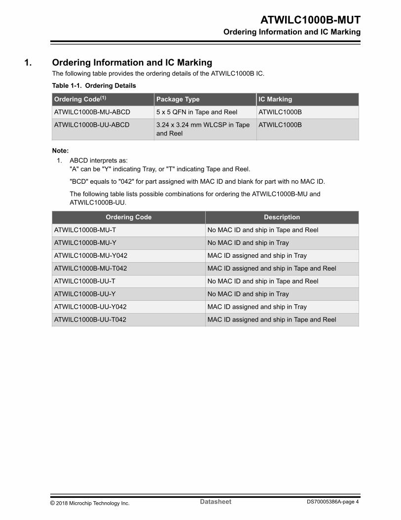
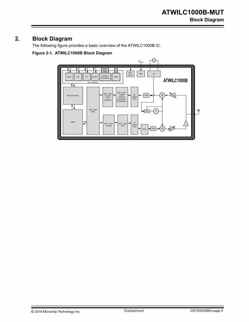
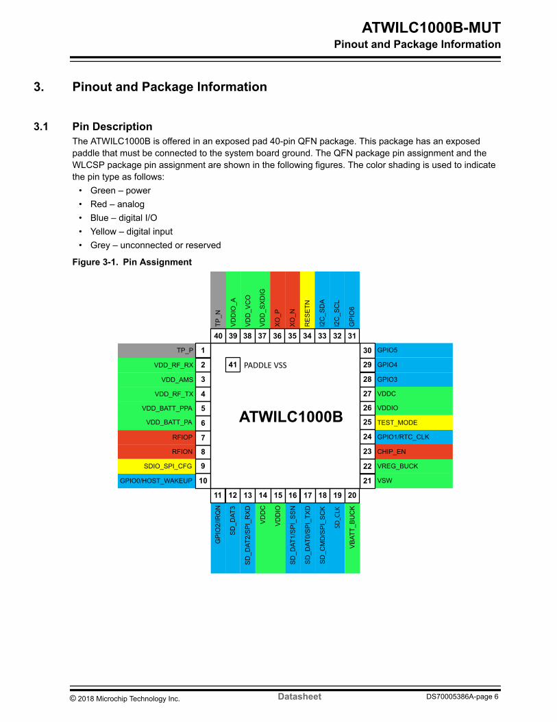
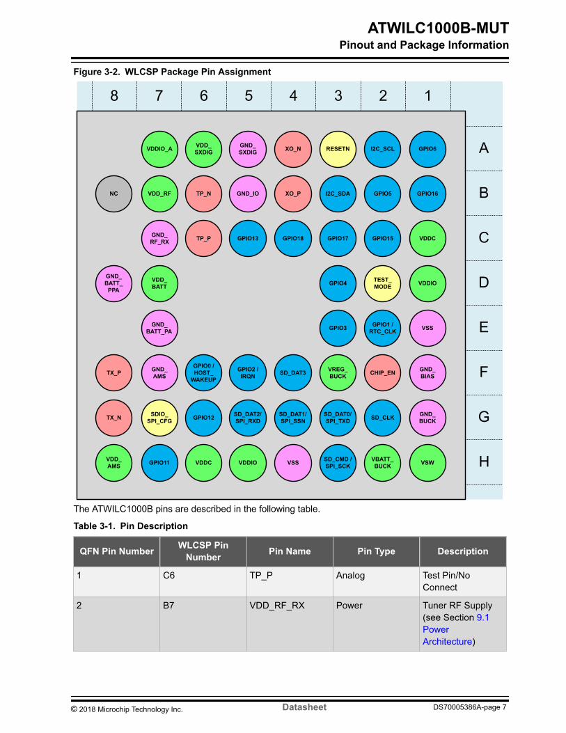
continued
QFN Pin Number WLCSP PinNumber Pin Name Pin Type Description
3 H8 VDD_AMS Power Tuner BB Supply(see Section 91 PowerArchitecture)
4 - VDD_RF_TX Power Tuner RF Supply(see Section 91 PowerArchitecture)
5 - VDD_BATT_PPA Power PA 1ST StageSupply (seeSection 91 PowerArchitecture)
6 D7 VDD_BATT_PA Power PA 2ND StageSupply (seeSection 91 PowerArchitecture)
7 - RFIOP Analog Positive RFDifferential IO (see Table 9-4)
8 - RFION Analog Negative RFDifferential IO (see Table 9-4)
9 G7 SDIO_SPI_CFG Digital Input Tie to 1 for SPI 0for SDIO
10 F6 GPIO0HOST_WAKE
Digital IOProgrammablePull-up
GPIO0SLEEPMode Control
11 F5 GPIO2IRQN Digital IOProgrammablePull-up
GPIO2DeviceInterrupt
12 F4 SD_DAT3 Digital IOProgrammablePull-up
SDIO Data3
13 G5 SD_DAT2SPI_RXD
Digital IOProgrammablePull-up
SDIO Data2SPIData RX
14 C1 VDDC Power Digital Core PowerSupply (seeSection 91 PowerArchitecture)
ATWILC1000B-MUTPinout and Package Information
copy 2018 Microchip Technology Inc Datasheet DS70005386A-page 8
continued
QFN Pin Number WLCSP PinNumber Pin Name Pin Type Description
15 D1 VDDIO Power Digital IO PowerSupply (seeSection 91 PowerArchitecture)
16 G4 SD_DAT1SPI_SSN
Digital IOProgrammablePull-up
SDIO Data1SPISlave Select
17 G3 SD_DAT0SPI_TXD
Digital IOProgrammablePull-up
SDIO Data0SPIData TX
18 H3 SD_CMDSPI_SCK
Digital IOProgrammablePull-up
SDIOCommandSPIClock
19 G2 SD_CLK Digital IOProgrammablePull-up
SDIO Clock
20 H2 VBATT_BUCK Power Battery Supply forDCDC Converter(see Section 91 PowerArchitecture)
21 H1 VSW Power Switching output ofDCDC Converter(see Section 91 PowerArchitecture)
22 F3 VREG_BUCK Power Core Power fromDCDC Converter(see Section 91 PowerArchitecture)
23 F2 CHIP_EN Analog PMU Enable
24 E2 GPIO1RTC_CLK Digital IOProgrammablePull-up
GPIO132kHzClock Input
25 D2 TEST_MODE Digital Input Test Mode ndash Usermust tie this pin toGND
ATWILC1000B-MUTPinout and Package Information
copy 2018 Microchip Technology Inc Datasheet DS70005386A-page 9
continued
QFN Pin Number WLCSP PinNumber Pin Name Pin Type Description
26 H5 VDDIO Power Digital IO PowerSupply (seeSection 91 PowerArchitecture)
27 H6 VDDC Power Digital Core PowerSupply (seeSection 91 PowerArchitecture)
28 E3 GPIO3 Digital IOProgrammablePull-up
GPIO3SPI_SCK_Flash
29 D3 GPIO4 Digital IOProgrammablePull-up
GPIO4SPI_SSN_Flash
30 B2 GPIO5 Digital IOProgrammablePull-up
GPIO5SPI_TXD_Flash
31 A1 GPIO6 Digital IOProgrammablePull-up
GPIO6SPI_RXD_Flash
32 A2 I2C_SCL Digital IOProgrammablePull-up
I2C Slave Clock(high-drive padsee Table 4-3)
33 B3 I2C_SDA Digital IOProgrammablePull-up
I2C Slave Data(high-drive padsee Table 4-3)
34 A3 RESETN Digital Input Active-Low HardReset
35 A4 XO_N Analog Crystal Oscillator N
36 B4 XO_P Analog Crystal Oscillator P
37 A6 VDD_SXDIG Power SX Power Supply(see Section 91 PowerArchitecture)
38 - VDD_VCO Power VCO Power Supply(see Section 91 PowerArchitecture)
ATWILC1000B-MUTPinout and Package Information
copy 2018 Microchip Technology Inc Datasheet DS70005386A-page 10
continued
QFN Pin Number WLCSP PinNumber Pin Name Pin Type Description
39 A7 VDDIO_A Power Tuner VDDIOPower Supply (seeSection 91 PowerArchitecture)
40 B6 TP_N Analog Test PinNoConnect
41(1) - PADDLE VSS Ground Connect to SystemBoard Ground
- A5 GND_SXDIG Ground SX GroundConnect to SystemBoard Ground
- B1 GPIO16 Digital IOProgrammablePull-up
GPIO16
- B5 GND_IO Ground IO GroundConnect to SystemBoard Ground
- B8 NC None ReservedNoConnect
- C2 GPIO15 Digital IOProgrammablePull-up
GPIO15
- C3 GPIO17 Digital IOProgrammablePull-up
GPIO17
- C4 GPIO18 Digital IOProgrammablePull-up
GPIO18
- C5 GPIO13 Digital IOProgrammablePull-up
GPIO13
- C7 GND_RF_RX Ground RF Rx GroundConnect to SystemBoard Ground
- D8 GND_BATT_PPA Ground PA 2nd StageGround Connectto System BoardGround
ATWILC1000B-MUTPinout and Package Information
copy 2018 Microchip Technology Inc Datasheet DS70005386A-page 11
continued
QFN Pin Number WLCSP PinNumber Pin Name Pin Type Description
- E1 VSS Ground Connect to SystemBoard Ground
- E7 GND_BATT_PA Ground PA 1st StageGround Connectto System BoardGround
- F1 GND_BIAS Ground Bias GroundConnect to SystemBoard Ground
- F7 GND_AMS Ground AMS GroundConnect to SystemBoard Ground
- F8 TX_P Analog Positive RFDifferential IO
- G1 GND_BUCK Ground DCDC ConverterGround Connectto System BoardGround
- G6 GPIO12 Digital IOProgrammablePull-up
GPIO12
- G8 TX_N Analog Negative RFDifferential IO
- H4 VSS Ground Connect to SystemBoard Ground
- H7 GPIO11 Digital IOProgrammablePull-up
GPIO11
Note 1 Applies to QFN package only Pin 41 PADDLE_VSS must be soldered to GND providing good RF
grounding and good heat dissipation
ATWILC1000B-MUTPinout and Package Information
copy 2018 Microchip Technology Inc Datasheet DS70005386A-page 12
Figure 3-3 WLCSP ATWILC1000B UU
32 Package DescriptionThe ATWILC1000B QFN package information is provided in the following table and the package view isshown in Figure 3-4
Table 3-2 QFN Package Information
Parameter Value Unit Tolerance
Package size 5 x 5 mm plusmn01 mm
QFN pad count 40 ndash ndash
Total thickness 085 mm +015-005mm
QFN pad pitch 040 ndash
Pad width 020 ndash
Exposed pad size 37 x 37 ndash
The ATWILC1000B WLCSP package information is provided in the following table and the package viewis shown in the Figure 3-5
Table 3-3 WLCSP Package Information
Parameter Value Unit Tolerance
Package size 324 x 324
mm
plusmn03 mm
Total thickness 056 plusmn03 mm
IO Pitch 035 ndash
Ball diameter 020 plusmn03 mm
ATWILC1000B-MUTPinout and Package Information
copy 2018 Microchip Technology Inc Datasheet DS70005386A-page 13
Figure 3-4 QFN Package
Figure 3-5 WLCSP Package
ATWILC1000B-MUTPinout and Package Information
copy 2018 Microchip Technology Inc Datasheet DS70005386A-page 14
4 Electrical Specifications
41 Absolute RatingsThe values listed in this section are the peaked excursions ratings that can be tolerated by the deviceand if sustained will cause irreparable damage to the device
Table 4-1 Absolute Maximum Ratings
Characteristics Symbol Min Max Unit
Core supply voltage VDDC -03 15
V
IO supply voltage VDDIO -03 50
Battery supply voltage VBATT -03 50
Digital input voltage VIN (1) -03 VDDIO
Analog input voltage VAIN (2) -03 15
ESD human body model VESDHBM (3) -1000 -2000 (3) +1000 +2000 (3)
Storage temperature TA -65 150ordmC
Junction temperature ndash ndash 125
RF input power max ndash ndash 23 dBm
Note 1 VIN corresponds to all the digital pins2 VAIN corresponds to the following analog pins VDD_RF_RX VDD_RF_TX VDD_AMS RFIOP
RFION XO_N XO_P VDD_SXDIG and VDD_VCO3 For VESDHBM each pin is classified as Class 1 or Class 2 or both
ndash The Class 1 pins include all the pins (both analog and digital)ndash The Class 2 pins are all digital pins onlyndash VESDHBM is plusmn1 kV for Class 1 pins VESDHBM is plusmn2 kV for Class 2 pins
42 Recommended Operating ConditionsThe recommended operating conditions for the ATWILC1000B are listed in the following table
Table 4-2 Recommended Operating Conditions
Characteristics Symbol Min Typ Max Unit
IO supply voltage VDDIO 27 33 36V
Battery supply voltage VBATT 300 330 420
Operating temperature ndash -40 ndash 85 ordmC
ATWILC1000B-MUTElectrical Specifications
copy 2018 Microchip Technology Inc Datasheet DS70005386A-page 15
Note 1 The ATWILC1000B is functional across this range of voltages however optimal RF performance is
ensured for VBATT in the range 30V lt VBATT lt 42V2 IO supply voltage is applied to the VDDIO_A and VDDIO pins3 Battery supply voltage is applied to the VDD_BATT_PPA VDD_BATT_PA and VBATT_BUCK pins4 See Table 9-4 for the details of power connections
43 DC Electrical CharacteristicsThe following table provides the DC characteristics for the ATWILC1000B digital pads
Table 4-3 DC Electrical Characteristics
Characteristic Min Typ Max Unit
Input Low Voltage(VIL)
-030 ndash 060
V
Input High Voltage(VIH)
VDDIO-060 ndash VDDIO+030
Output LowVoltage (VOL)
ndash ndash 045
Output HighVoltage (OVOH)
VDDIO-050 ndash ndash
Output Loading ndash ndash 20pF
Digital Input Load ndash ndash 6
Pad Drive Strength(regular pads (1))
106 135 ndash
mAPad Drive Strength(high-drive pads (1))
212 27 ndash
Note 1 The following are high-drive pads I2C_SCL I2C_SDA all other pads are regular
ATWILC1000B-MUTElectrical Specifications
copy 2018 Microchip Technology Inc Datasheet DS70005386A-page 16
5 Clocking
51 Crystal OscillatorThe following table provides the crystal oscillator parameters of the ATWILC1000B
Table 5-1 Crystal Oscillator Parameters
Parameter Min Typ Max Unit
Crystal resonant frequency ndash 26 ndash MHz
Crystal equivalent series resistance ndash 50 150 Ω
Stability ndash Initial offset(1) -100 ndash 100ppm
Stability - Temperature and aging -25 ndash 25
Note 1 To ensure plusmn25 ppm under operating conditions frequency offset calibration is required
The following block diagram in figure XO Connections - (a) shows how the internal Crystal Oscillator(XO) is connected to the external crystal The XO has 5 pF internal capacitance (denoted as c_onchip inthe following figure) on each terminal XO_P and XO_N To bypass the crystal oscillator with an externalreference an external signal capable of driving 5 pF can be applied to the XO_N terminal as shown infollowing figure XO Connections - (b) The XO has 5 pF internal capacitance on each terminal XO_Pand XO_N This internal capacitance must be accounted for when calculating the external loadingcapacitance c_onboard for the XTAL
Figure 5-1 XO Connections (a) The Crystal Oscillator is Used (b) The Crystal Oscillator isBypassed
XO_N XO_P XO_N XO_P
External Clock
ATWILC1000 ATWILC1000
(a) (b)
c_onboard c_onboard
c_onchip c_onchip
The following table specifies the electrical and performance requirements for the external clock
ATWILC1000B-MUTClocking
copy 2018 Microchip Technology Inc Datasheet DS70005386A-page 17
Table 5-2 Bypass Clock Specification
Parameter Min Typ Max Unit Comments
Oscillationfrequency ndash 26 ndash MHz
Must drive 5 pFload at desiredfrequency
Voltage swing 05 ndash 12 VPPMust be ACcoupled
Stability ndashTemperatureand aging
-25ndash
+25 ppmndash
Phase noise ndash ndash -130 dBcHz At 10 kHz offset
Jitter (RMS) ndash ndash
lt1
psec Based onintegratedphase noisespectrum from1 kHz to 1 MHz
52 Low-Power OscillatorThe ATWILC1000B has an internally-generated 32 kHz clock to provide timing information for varioussleep functions Alternatively the ATWILC1000B allows for an external 32kHz clock to be used for thispurpose which is provided through pin 24 (RTC_CLK) Software selects whether the internal clock orexternal clock is used
The internal low-power clock is ring oscillator-based and has accuracy within 10000 ppm When usingthe internal low-power clock the advance wake-up time in the Beacon Monitoring mode has to beincreased by about 1 of the sleep time to compensate for the oscillator inaccuracy For example for theDTIM interval value of 1 wake-up time has to be increased by 1 ms
For any application targeting very low-power consumption an external 32 kHz RTC clock must be used
ATWILC1000B-MUTClocking
copy 2018 Microchip Technology Inc Datasheet DS70005386A-page 18
6 CPU and Memory Subsystem
61 ProcessorThe ATWILC1000B has a Cortus APS3 32-bit processor This processor performs many of the MACfunctions including but not limited to association authentication power management security keymanagement and MSDU aggregationde-aggregation In addition the processor provides flexibility forvarious modes of operation such as STA and AP modes
62 Memory SubsystemThe APS3 core uses a 128 KB instructionboot ROM along with a 160 KB instruction RAM and a 64 KBdata RAM In addition the device uses a 128 KB shared RAM accessible by the processor and MACwhich allows the APS3 core to perform various data management tasks on the TX and RX data packets
63 Nonvolatile Memory (eFuse)The ATWILC1000B has 768 bits of nonvolatile eFuse memory that can be read by the CPU after devicereset This nonvolatile One-Time-Programmable (OTP) memory can be used to store customer-specificparameters such as MAC address various calibration information such as TX power crystal frequencyoffset other software-specific configuration parameters and so on The eFuse is partitioned into six 128-bit banks Each bank has the same bit map which is shown in the following figure The purpose of thefirst 80 bits in each bank is fixed and the remaining 48 bits are general-purpose software dependent bitsor reserved for future use Since each bank can be programmed independently this allows for severalupdates of the device parameters following the initial programming eg updating the MAC addressRefer to the ATWILC1000 Programming Guide for the eFuse programming instructions
ATWILC1000B-MUTCPU and Memory Subsystem
copy 2018 Microchip Technology Inc Datasheet DS70005386A-page 19
Figure 6-1 eFuse Bit Map
Bank 0
Bank 1
Bank 2
Bank 3
Bank 4
Bank 5
F MAC ADDR
Used
Inva
lid
Version
Reserved
MACAD
DR
Used
FO
Flags
G
21 1 3 1
Use
d
TX Gain
Correct-
tion
Used
Freq
Offse
t
1 7
488 8 16
1 15
128 Bits
ATWILC1000B-MUTCPU and Memory Subsystem
copy 2018 Microchip Technology Inc Datasheet DS70005386A-page 20
7 WLAN SubsystemThe WLAN subsystem is composed of the Media Access Controller (MAC) and the Physical Layer (PHY)The following two subsections describe the MAC and PHY in detail
71 MAC
711 FeaturesThe ATWILC1000B IEEE80211 MAC supports the following functions
bull IEEE 80211bgnbull IEEE 80211e WMM QoS EDCAPCF Multiple Access Categories Traffic Schedulingbull Advanced IEEE 80211n Features
ndash Transmission and reception of aggregated MPDUs (A-MPDU)ndash Transmission and reception of aggregated MSDUs (A-MSDU)ndash Immediate Block Acknowledgmentndash Reduced Interframe Spacing (RIFS)
bull Support for IEEE 80211i and WFA Security with Key Managementndash WEP 64128ndash WPA-TKIPndash 128-bit WPA2 CCMP (AES)
bull Support for WAPI Securitybull Advanced Power Management
ndash Standard 80211 Power Save modendash Wi-Fi Alliancereg WMM-PS (U-APSD)
bull RTS-CTS and CTS-Self Supportbull Supports Either STA or AP Mode in the Infrastructure Basic Service Set Modebull Supports Independent Basic Service Set (IBSS)
712 DescriptionThe ATWILC1000B MAC is designed to operate at low power while providing high data throughput TheIEEE 80211 MAC functions are implemented with a combination of dedicated datapath engineshardwired control logic and a low-power high-efficiency microprocessor The combination of dedicatedlogic with a programmable processor provides optimal power efficiency and real-time response whileproviding the flexibility to accommodate evolving standards and future feature enhancements
Dedicated datapath engines with heavy computational are used to implement datapath functions Forexample an FCS engine checks the CRC of the transmitting and receiving packets and a cipher engineperforms all the required encryption and decryption operations for the WEP WPA-TKIP WPA2 CCMP-AES and WAPI security requirements
Control functions which have real-time requirements are implemented using hardwired control logicmodules These logic modules offer real-time response while maintaining configurability via theprocessor Examples of hardwired control logic modules are the channel access control module(implements EDCAHCCA Beacon TX control interframe spacing and so on) protocol timer module(responsible for the Network Access Vector back-off timing timing synchronization function and slotmanagement) MPDU handling module aggregationdeaggregation module block ACK controller
ATWILC1000B-MUTWLAN Subsystem
copy 2018 Microchip Technology Inc Datasheet DS70005386A-page 21
(implements the protocol requirements for burst block communication) and TXRX control FSMs(coordinate data movement between PHY-MAC interface cipher engine and the DMA interface to theTXRX FIFOs)
The MAC functions that are implemented in software on the microprocessor have the followingcharacteristics
bull Functions with high memory requirements or complex data structures Examples are associationtable management and power save queuing
bull Functions with low computational load or without critical real-time requirements Examples areauthentication and association
bull Functions which need flexibility and upgradeability Examples are beacon frame processing and QoSscheduling
72 PHY
721 FeaturesThe ATWILC1000B IEEE 80211 PHY supports the following functions
bull Single Antenna 1x1 Stream in 20 MHz Channelsbull Supports IEEE 80211b DSSS-CCK Modulation 1 2 55 and 11 Mbpsbull Supports IEEE 80211g OFDM Modulation 6 9 1218 24 36 48 and 54 Mbpsbull Supports IEEE 80211n HT Modulations MCS0-7 20 MHz 800 and 400 ns guard interval 65 72
130 144 195 217 260 289 390 433 520 578 585 650 and 722 Mbpsbull IEEE 80211n Mixed Mode Operationbull Per Packet TX Power Controlbull Advanced Channel EstimationEqualization Automatic Gain Control CCA CarrierSymbol Recovery
and Frame Detection
722 DescriptionThe ATWILC1000B WLAN PHY is designed to achieve reliable and power-efficient physical layercommunication specified by IEEE 80211 bgn in Single Stream mode with 20 MHz bandwidth Advancedalgorithms are used to achieve maximum throughput in a real-world communication environment withimpairments and interference The PHY implements all the required functions such as FFT filtering FEC(Viterbi decoder) frequency and timing acquisition and tracking channel estimation and equalizationcarrier sensing and clear channel assessment as well as the automatic gain control
73 RadioThis section describes the properties and characteristics of the ATWILC1000B and Wi-Fi radio transmitand receive performance capabilities of the device The performance measurements are taken at the RFpin assuming 50Ω impedance the RF performance is assured for room temperature of 25degC with aderating of 2-3dB at boundary conditions
Measurements were taken under typical conditions VBATT at 33V VDDIO at 33V and temperature at+25ordmC
ATWILC1000B-MUTWLAN Subsystem
copy 2018 Microchip Technology Inc Datasheet DS70005386A-page 22
Table 7-1 Features and Properties
Feature Description
Part Number ATWILC1000B
WLAN Standard IEEE 80211bgn Wi-Fi compliant
Host Interface SPI SDIO
Dimension L x W x H 217 x 147 x 21 (typical) mm
Frequency range 2412 GHz ~ 2472 GHz (24 GHz ISM band)
Number of channels 11 for North America 13 for Europe
Modulation 80211b DQPSK DBPSK CCK
80211gn OFDM64-QAM16-QAM QPSK BPSK
Data rate 80211b 1 2 55 11 Mbps80211g 6 9 12 18 24 36 48 54 Mbps
Data rate
(20 MHz short GI400ns)
80211n 72 144 217 289 433 578 65722Mbps
Operating temperature(1) -40degC to 85degC
Storage temperature -40degC to 125degC
Humidity Operating humidity 10 to 95 non-condensing
Storage humidity 5 to 95 non-condensing
Note 1 RF performance is ensured at room temperature of 25degC with a 2-3db change at boundary
conditions
731 Receiver PerformanceThe following are typical conditions for radio receiver performance
VBATT at 33V VDDIO at 33V temperature at 25degC and WLAN Channel 6 (2437 MHz)
The table below provides the receiver performance characteristics for the ATWILC1000B
Table 7-2 Receiver Performance
Parameter Description Min Typ Max Unit
Frequency - 2412 - 2472 MHz
Sensitivity 80211b 1 Mbps DSSS - -94 -
dBm2 Mbps DSSS - -91 -
55 Mbps DSSS - -89 -
11 Mbps DSSS - -86 -
ATWILC1000B-MUTWLAN Subsystem
copy 2018 Microchip Technology Inc Datasheet DS70005386A-page 23
continuedParameter Description Min Typ Max Unit
Sensitivity 80211g 6 Mbps OFDM - -88 -
dBm
9 Mbps OFDM - -87 -
12 Mbps OFDM - -86 -
18 Mbps OFDM - -84 -
24 Mbps OFDM - -82 -
36 Mbps OFDM - -78 -
48 Mbps OFDM - -74 -
54 Mbps OFDM - -73 -
Sensitivity 80211n (BW at 20 MHz) MCS 0 - -87 -
dBm
MCS 1 - -85 -
MCS 2 - -83 -
MCS 3 - -80 -
MCS 4 - -76 -
MCS 5 - -73 -
MCS 6 - -71 -
MCS 7 - -69 -
Maximum Receive Signal Level 1-11 Mbps DSSS - 0 -
dBm6-54 Mbps OFDM - -5 -
MCS 0 ndash 7 - -5 -
Adjacent Channel Rejection 1 Mbps DSSS (30 MHz offset) - 50 -
dB
11 Mbps DSSS (25 MHz offset) - 43 -
6 Mbps OFDM (25 MHz offset) - 40 -
54 Mbps OFDM (25 MHz offset) - 25 -
MCS 0 ndash 20 MHz BW (25 MHz offset) - 40 -
MCS 7 ndash 20 MHz BW (25 MHz offset) - 20 -
ATWILC1000B-MUTWLAN Subsystem
copy 2018 Microchip Technology Inc Datasheet DS70005386A-page 24
continuedParameter Description Min Typ Max Unit
Cellular Blocker Immunity 776-794 MHz CDMA - -14 -
dBm
824-849 MHz GSM - -10 -
880-915 MHz GSM - -10 -
1710-1785 MHz GSM - -15 -
1850-1910 MHz GSM - -15 -
1850-1910 MHz WCDMA - -24 -
1920-1980 MHz WCDMA - -24 -
732 Transmitter PerformanceThe following are typical conditions for radio transmitter performance
VBAT=33V VDDIO=33V temperature at 25degC and WLAN Channel 6 (2437 MHz)
The following table provides the transmitter performance characteristics for the ATWILC1000B
Table 7-3 Transmitter Performance
Parameter Description Min Typ Max Unit
Frequency - 2412 2472 MHz
Output power(1)-(2)ON_Transmit
80211b 1Mbps - 176 -
dBm
80211b 11Mbps - 182 -
80211g 6Mbps - 187 -
80211g 54Mbps - 167 -
80211n MCS 0 - 173 -
80211n MCS 7 - 138 -
TX power accuracy - - plusmn15 (2) dB
Carrier suppression 80211b mode - -194 -
dBc80211g mode - -275 -
80211n mode - -211 -
ATWILC1000B-MUTWLAN Subsystem
copy 2018 Microchip Technology Inc Datasheet DS70005386A-page 25
continuedParameter Description Min Typ Max Unit
Out of band Transmit Power 76-108 - -125 -
dBmHz
776-794 - -125 -
869-960 - -125 -
925-960 - -125 -
1570-1580 - -125 -
1805-1880 - -125 -
1930-1990 - -125 -
2110-2170 - -125 -
Harmonic output power(4) 2nd - -28 -
dBmMHz3rd - -33 -
4th - -40 -
5th - -28 -
Note 1 Measured at 80211 specification compliant EVMSpectral mask2 Measured after RF matching network3 Operating temperature range is -40ordmC to +85ordmC RF performance is ensured at a room temperature
range of 25ordmC with 2-3dB change at boundary conditions4 Measured at 11 Mbps DG (Digital Gain) = -7 WLAN Channel 6 (2437 MHz)5 With respect to TX power different (higherlower) RF output power settings may be used for
specific antennas andor enclosures in which case re-certification may be required6 The availability of some specific channels andor operational frequency bands are country
dependent and should be programmed at the host product factory to match the intendeddestination Regulatory bodies prohibit exposing the settings to the end user This requirementneeds to be taken care of via host implementation
ATWILC1000B-MUTWLAN Subsystem
copy 2018 Microchip Technology Inc Datasheet DS70005386A-page 26
8 External InterfacesThe ATWILC1000B external interfaces include
bull I2C slave for controlbull SPI slave and SDIO slave for control and data transferbull SPI master for external Flashbull I2C master for external EEPROMbull UART Debug Interfacebull General Purpose InputOutput (GPIO) pins
81 I2C Slave InterfaceThe I2C Slave interface used primarily for control by the host processor is a two-wire serial interfaceconsisting of a serial data line (SDA Pin 33) and a serial clock (SCL pin 32) It responds to the seven bitaddress value 0x60 The ATWILC1000B I2C supports I2C bus Version 21 - 2000 and can operate inStandard mode (with data rates up to 100 Kbs) and Fast mode (with data rates up to 400 Kbs) The I2CSlave is a synchronous serial interface The SDA line is a bidirectional signal and changes only while theSCL line is low except for STOP START and RESTART conditions The output drivers are open-drain toperform wire-AND functions on the bus The maximum number of devices on the bus is limited by onlythe maximum capacitance specification of 400 pF Data is transmitted in byte packages For specificinformation refer to the Philips Specification entitled ldquoThe I2C -Bus Specification Version 21rdquo The I2CSlave timing is provided in the following figure
Figure 8-1 I2C Slave Timing Diagram
tHL
SDA
SCL tHDSTA
tWL
tWH
tSUDAT tPR tHDDAT
tPR tPR
tLH tHL
tLH
tSUSTOtBUF
tSUSTAfSCL
The I2C Slave timing parameters are provided in the following table
Table 8-1 I2C Slave Timing Parameters
Parameter Symbol Min Max Unit Remarks
SCL clock frequency fSCL 0 400 kHz ndash
SCL low pulse width tWL 13 ndashmicros
ndash
SCL high pulse width tWH 06 ndash ndash
ATWILC1000B-MUTExternal Interfaces
copy 2018 Microchip Technology Inc Datasheet DS70005386A-page 27
continuedParameter Symbol Min Max Unit Remarks
SCL SDA fall time tHL ndash 300ns
ndash
SCL SDA rise time tLH ndash 300 This is dictated by externalcomponents
START setup time tSUSTA 06 ndashmicros
ndash
START hold time tHDSTA 06 ndash ndash
SDA setup time tSUDAT 100 ndash
ns
ndash
SDA hold time tHDDAT 0
40
ndash Slave and master default masterprogramming option
STOP setup time tSUSTO 06 ndashmicros
ndash
Bus free time between STOP and START tBUF 13 ndash ndash
Glitch pulse reject tPR 0 50 ns ndash
82 I2C Master InterfaceThe ATWILC1000B provides an I2C bus master which is intended primarily for accessing an externalEEPROM memory through a software-defined protocol The I2C Master is a two-wire serial interfaceconsisting of a serial data line (SDA) and a serial clock line (SCL) SDA can be configured on one of thefollowing pins SD_CLK (pin 19) GPIO1 (pin 24) GPIO6 (pin 31) or I2C_SDA (pin 33) SCL can beconfigured on one of the following pins GPIO0 (pin 10) SD_DAT3 (pin 12) GPIO4 (pin 29) or I2C_SCL(pin 32) For more specific instructions refer to the ATWILC1000 Programming Guide
The I2C master interface supports three speeds
bull Standard mode (100 kbs)bull Fast mode (400 kbs)bull High-Speed mode (34 Mbs)
The timing diagram of the I2C master interface is the same as that of the I2C slave interface (see Figure8-1) The timing parameters of I2C master are shown in the following table
Table 8-2 I2C Master Timing Parameters
Parameter Symbol Standard Mode Fast Mode High-Speed Mode Unit
Min Max Min Max Min Max
SCL clock frequency fSCL 0 100 0 400 0 3400 kHz
SCL high pulse width tWH 4 ndash 06 ndash 006 ndashmicros
SCL low pulse width tWL 47 ndash 13 ndash 016 ndash
ATWILC1000B-MUTExternal Interfaces
copy 2018 Microchip Technology Inc Datasheet DS70005386A-page 28
continuedParameter Symbol Standard Mode Fast Mode High-Speed Mode Unit
Min Max Min Max Min Max
SCL fall time tHLSCL ndash 300 ndash 300 10 40
nsSDA fall time tHLSDA ndash 300 300 10 80
SCL rise time tLHSCL ndash 1000 ndash 300 10 40
SDA rise time tLHSDA ndash 1000 ndash 300 10 80
START setup time tSUSTA 47 ndash 06 ndash 016 ndashmicros
START hold time tHDSTA 4 ndash 06 ndash 016 ndash
SDA setup time tSUDAT 250 ndash 100 ndash 10 ndashns
SDA hold time tHDDAT 5 ndash 40 ndash 0 70
STOP setup time tSUSTO 4 ndash 06 ndash 016 ndash
microsBus free time between STOP andSTART
tBUF 47 ndash 13 ndash ndash ndash
Glitch pulse reject tPR ndash ndash 0 50 ndash ndash
83 SPI Slave InterfaceThe ATWILC1000B provides a Serial Peripheral Interface (SPI) that operates as an SPI slave The SPISlave interface can be used for control and for serial IO of 80211 data The SPI Slave pins are mappedas shown in the the following table The RXD pin is same as Master Output Slave Input (MOSI) and theTXD pin is same as Master Input Slave Output (MISO) The SPI Slave is a full-duplex slave-synchronousserial interface that is available immediately following reset when pin 9 (SDIO_SPI_CFG) is tied toVDDIO
Table 8-3 SPI Slave Interface Pin Mapping
Pin Number SPI Function
9 CFG Must be tied to VDDIO
16 SSN Active Low Slave Select
18 SCK Serial Clock
13 RXD Serial Data Receive (MOSI)
17 TXD Serial Data Transmit (MISO)
When the SPI is not selected ie when SSN is high the SPI interface does not interfere with datatransfers between the serial-master and other serial-slave devices When the serial slave is not selectedits transmitted data output is buffered resulting in a high impedance drive onto the serial master receiveline
The SPI Slave interface responds to a protocol that allows an external host to read or write any register inthe chip as well as initiate DMA transfers For more details of the SPI protocol and more specificinstructions refer to the ATWILC1000 Programming Guide
ATWILC1000B-MUTExternal Interfaces
copy 2018 Microchip Technology Inc Datasheet DS70005386A-page 29
The SPI Slave interface supports four standard modes as determined by the Clock Polarity (CPOL) andClock Phase (CPHA) settings These modes are illustrated in table SPI Slave Modes and Figure 8-2 Thered lines in this figure correspond to Clock Phase = 0 and the blue lines correspond to Clock Phase = 1
Table 8-4 SPI Slave Modes
Mode CPOL CPHA
0 0 0
1 0 1
2 1 0
3 1 1
Figure 8-2 SPI Slave Clock Polarity and Clock Phase Timing
z
z z
z
SCKCPOL = 0
CPOL = 1
SSN
RXDTXD(MOSIMISO)
CPHA = 0
CPHA = 1
2 3 4 5 6 7 8
1 2 3 4 5 6 7
1
8
The SPI slave timing is provided in the following figure
ATWILC1000B-MUTExternal Interfaces
copy 2018 Microchip Technology Inc Datasheet DS70005386A-page 30
Figure 8-3 SPI Slave Timing Diagram
The SPI slave timing parameters are provided in the following table
Table 8-5 SPI Slave Timing Parameters
Parameter Symbol Min Max Unit
Clock input frequency fSCK ndash 48 MHz
Clock low pulse width tWL 15 ndash
ns
Clock high pulse width tWH 15 ndash
Clock rise time tLH ndash 10
Clock fall time tHL ndash 10
Input setup time tISU 5 ndash
Input hold time tIHD 5 ndash
Output delay tODLY 0 20
Slave select setup time tSUSSN 5 ndash
Slave select hold time tHDSSN 5 ndash
84 SPI Master InterfaceThe ATWILC1000B provides an SPI master interface for accessing external Flash memory The SPImaster pins are mapped as shown in the following table The TXD pin is same as Master Output SlaveInput (MOSI) and the RXD pin is same as Master Input Slave Output (MISO) The SPI master interfacesupports all four standard modes of clock polarity and clock phase shown in Table 8-4 External SPI Flash
ATWILC1000B-MUTExternal Interfaces
copy 2018 Microchip Technology Inc Datasheet DS70005386A-page 31
memory is accessed by a processor programming commands to the SPI master interface which in turninitiates a SPI master access to the Flash For more specific instructions refer to the ATWILC1000Programming Guide
Table 8-6 SPI Master Interface Pin Mapping
Pin Number Pin Name SPI Function
28 GPIO3 SCK Serial Clock Output
29 GPIO4 SCK Active-Low Slave Select Output
30 GPIO5 TXD Serial Data Transmit Output (MOSI)
31 GPIO6 RXD Serial Data Receive Input (MISO)
The SPI master timing is provided in the following figure
Figure 8-4 SPI Master Timing Diagram
fSCK
tWHtLH
tHL
tWL
tODLY tISU tIHD
SCK
SSNTXD
RXD
The SPI master timing parameters are provided in the following table
Table 8-7 SPI Master Timing Parameters
Parameter Symbol Min Max Unit
Clock output frequency fSCK ndash 48 MHz
Clock low pulse width tWL 5 ndash
ns
Clock high pulse width tWH 5 ndash
Clock rise time tLH ndash 5
Clock fall time tHL ndash 5
Input setup time tISU 5 ndash
Input hold time tIHD 5 ndash
Output delay tODLY 0 5
ATWILC1000B-MUTExternal Interfaces
copy 2018 Microchip Technology Inc Datasheet DS70005386A-page 32
85 SDIO Slave InterfaceThe ATWILC1000B SDIO Slave is a full speed interface The interface supports the 1-bit4-bit SDTransfer mode at the clock range of 0 to 50 MHz The host can use this interface to read and write fromany register within the chip as well as configure the ATWILC1000B for data DMA To use this interfacepin 9 (SDIO_SPI_CFG) must be grounded The SDIO slave pins are mapped as shown in the followingtable
Table 8-8 SDIO Interface Pin Mapping
Pin Number SPI Function
9 CFG Must be tied to ground
12 DAT3 Data 3
13 DAT2 Data 2
16 DAT1 Data 1
17 DAT0 Data 0
18 CMD Command
19 CLK Clock
When the SDIO card is inserted into an SDIO aware host the detection of the card will be via the meansdescribed in SDIO specification During the normal initialization and interrogation of the card by the hostthe card identifies itself as an SDIO device The host software obtains the card information in a tuple(linked list) format and determines if that cardrsquos IO function(s) are acceptable to activate If the card isacceptable it is allowed to power-up fully and start the IO function(s) built into it The SD memory cardcommunication is based on an advanced 9-pin interface (clock command four data and three powerlines) designed to operate at a maximum operating frequency of 50 MHz The SDIO slave interface hasthe following features
bull Meets SDIO card specification version 20bull Host clock rate variable between 0 to 50 MHzbull 1 bit4-bit SD bus modes supportedbull Allows card to interrupt hostbull Responds to direct readwrite (IO52) and extended readwrite (IO53) transactionsbull Supports SuspendResume operation
The SDIO slave interface timing is provided in the following figure
ATWILC1000B-MUTExternal Interfaces
copy 2018 Microchip Technology Inc Datasheet DS70005386A-page 33
Figure 8-5 SDIO Slave Timing Diagram
The SDIO slave timing parameters are provided in the following table
Table 8-9 SDIO Slave Timing Parameters
Parameter Symbol Min Max Unit
Clock input frequency fPP 0 50 MHz
Clock low pulse width tWL 10 ndash
ns
Clock high pulse width tWH 10 ndash
Clock rise time tLH ndash 10
Clock fall time tHL ndash 10
Input setup time tISU 5 ndash
Input hold time tIH 5 ndash
Output delay tODLY 0 14
86 UART Debug InterfaceATWILC1000B has a Universal Asynchronous ReceiverTransmitter (UART) interface on pin 13 SD-DATA2SPI-RxD and pin 17 SD-DATA0SPI-TXD This interface should be used only for debuggingpurposes The UART is compatible with the RS-232 standard where ATWILC1000B-MUT operates asData Terminal Equipment (DTE) It has a two-pin RXDTXD interface
The default configuration for accessing the UART interface of ATWILC1000B-MUT is as followsbull Baud rate 115200bull Data 8 bitbull Parity None
ATWILC1000B-MUTExternal Interfaces
copy 2018 Microchip Technology Inc Datasheet DS70005386A-page 34
bull Stop bit 1 bitbull Flow control None
It also has Rx and Tx FIFOs which ensures reliable high speed reception and low software overheadtransmission FIFO size is 4x8 for both Rx and Tx direction The UART has status registers that show thenumber of received characters available in the FIFO and various error conditions in addition it has theability to generate interrupts based on these status bits
An example of UART receiving or transmitting a single packet is shown in the following figure Thisexample shows 7-bit data (0x45) odd parity and two stop bits
Figure 8-6 Example of UART RX or TX Packet
87 GPIOsNine General Purpose InputOutput (GPIO) pins labeled GPIO 0-8 are available to allow for applicationspecific functions Each GPIO pin can be programmed as an input (the value of the pin can be read bythe host or internal processor) or as an output (the output values can be programmed by the host orinternal processor) where the default mode after power-up is input GPIOs 7 and 8 are only availablewhen the host does not use the SDIO interface which shares two of its pins with these GPIOs Thereforefor SDIO-based applications seven GPIOs (0-6) are available For more specific usage instructions referto the ATWILC1000 Programming Guide
ATWILC1000B-MUTExternal Interfaces
copy 2018 Microchip Technology Inc Datasheet DS70005386A-page 35
9 Power Management
91 Power ArchitectureThe ATWILC1000B uses an innovative power architecture to eliminate the need for external regulatorsand reduce the number of off-chip components This architecture is shown in the following figure ThePower Management Unit (PMU) has a DCDC Converter that converts VBATT to the core supply used bythe digital and RFAMS blocks The PA and eFuse are supplied by dedicated LDOs and the VCO issupplied by a separate LDO structure The power connections in the following figure provide a conceptualframework for understanding the ATWILC1000B power architecture
Figure 9-1 Power Architecture
VBATT _BUCKOff-Chip
LC
RFAMS Core
Sleep Osc RF
AM
S C
ore
Volta
ge
VSW
VREG_BUCK
VDD_AMS VDD_RF VDD_SXDIG
LDO1VDDIO_A VDD_VCO
LDO2
~VDD_BATT
12V
10V
CHIP_EN
EFuse LDO
SX
Digital Core
DCDC Converter
EFuse
PA
PMU
RFAMS
DigitalVDDC
Dig CoreLDO
25V
PadsVDDIO
SleepLDO
Digital Core Voltage
dcdc_ena
enaena
Vin Vout
enaena
The following table provides the typical values for the digital and RFAMS core voltages
ATWILC1000B-MUTPower Management
copy 2018 Microchip Technology Inc Datasheet DS70005386A-page 36
Table 9-1 PMU Output Voltages
Parameter Typical
RFAMS core voltage (VREG_BUCK) 135V
Digital core voltage (VDDC) 110V
Refer to the reference design for an example of power supply connections including proper isolation ofthe supplies used by the digital and RFAMS blocks
92 Power ConsumptionThe ATWILC1000B has several device states
bull ON_Transmit ndash Device is actively transmitting an 80211 signalbull ON_Receive ndash Device is actively receiving an 80211 signalbull ON_Doze ndash Device is on but is neither transmitting nor receivingbull Power_Down ndash Device core supply off (leakage)
The following pins are used to switch between the ON and Power_Down statesbull CHIP_EN ndash Device pin (pin 23) used to enable DCDC Converterbull VDDIO ndash IO supply voltage from external supply
In the ON states VDDIO is on and CHIP_EN is high (at VDDIO voltage level) To switch between the ONstates and Power_Down state CHIP_EN has to change between high and low (GND) voltage WhenVDDIO is off and CHIP_EN is low the chip is powered off with no leakage (also see 93 Power-UpDownSequence)
921 Current Consumption in Various Device StatesThe following table provides the ATWILC1000B current consumption in various device states
Table 9-2 Current Consumption
Device State Code Rate Output Power(dBm)
Current Consumption(1)
IVBATT IVDDIO
ON_Transmit 80211b 1 Mbps 176 266 mA 22 mA
80211b 11 Mbps 185 239 mA 22 mA
80211g 6 Mbps 186 249 mA 22 mA
80211g 54 Mbps 169 173 mA 22 mA
80211n MCS 0 177 253 mA 22 mA
80211n MCS 7 140 164 mA 22 mA
ATWILC1000B-MUTPower Management
copy 2018 Microchip Technology Inc Datasheet DS70005386A-page 37
continuedDevice State Code Rate Output Power
(dBm)Current Consumption(1)
IVBATT IVDDIO
ON_Receive 80211b 1 Mbps NA 63 mA 22 mA
80211b 11 Mbps NA 63 mA 22 mA
80211g 6 Mbps NA 63 mA 22 mA
80211g 54 Mbps NA 63 mA 22 mA
80211n MCS 0 NA 63 mA 22 mA
80211n MCS 7 NA 63 mA 22 mA
ON_Doze NA NA 380 microA lt10 microA
Power_Down NA NA 125 μA (2)
Note 1 The power consumption values are measured when VBAT is 36V and VDDIO is 28V at 25degC
922 Controlling the Device StatesTable Device States shows how to switch between the device states using the following
bull CHIP_EN ndash Device pin (pin 23) used to enable DCDC Converterbull VDDIO ndash IO supply voltage from external supply
Table 9-3 Device States
Device State CHIP_EN VDDIO Power Consumption (1) (2)
IVBATT IVDDIO
ON_Transmit VDDIO On 172mA 18dBm (le18Mbps)
230mA 18dBm (gt18Mbps)
2mA
ON_Receive VDDIO On 60mA 2mA
ON_Doze VDDIO ON 280μA lt10μA
Power_Down GND On lt05μA lt02μA
Note 1 Conditions VBAT 36v IO18V2 Power consumption numbers are preliminary
923 Restrictions for Power StatesWhen no power is supplied to the device ie the DCDC converter output and VDDIO are both off (atground potential) In this case a voltage cannot be applied to the device pins because each pin containsan ESD diode from the pin to supply This diode turns on when voltage higher than one diode-drop issupplied to the pin
If a voltage must be applied to the signal pads while the chip is in a low power state the VDDIO supplymust be on so the SLEEP or Power_Down state must be used
ATWILC1000B-MUTPower Management
copy 2018 Microchip Technology Inc Datasheet DS70005386A-page 38
Similarly to prevent the pin-to-ground diode from turning on do not apply a voltage that is more than onediode-drop below ground to any pin
93 Power-UpDown SequenceThe power-updown sequence for the ATWILC1000B is shown in the following figure
Figure 9-2 Power-UpDown Sequence
VBATT
VDDIO
CHIP_EN
RESETN
tBIO
t IOCE
tCER
XO Clock
The timing parameters are provided in the following table
Table 9-4 Power-UpDown Sequence Timing
Parameter Min Max Unit Description Notes
tA 0 ndash
ms
VBATT rise to VDDIOrise
VBATT and VDDIO can rise simultaneously orcan be tied together VDDIO must not risebefore VBATT
tB 0 ndash VDDIO rise toCHIP_EN rise
CHIP_EN must not rise before VDDIOCHIP_EN must be driven high or low not leftfloating
tC 5 ndash CHIP_EN rise toRESETN rise
This delay is needed because XO clock muststabilize before RESETN removal RESETNmust be driven high or low not left floating
tA 0 ndash VDDIO fall to VBATTfall
VBATT and VDDIO can fall simultaneously orcan be tied together VBATT must not fall beforeVDDIO
tB 0 ndash CHIP_EN fall to VDDIOfall
VDDIO must not fall before CHIP_ENCHIP_EN and RESETN can fall simultaneously
tC 0 ndash RESETN fall to VDDIOfall
VDDIO must not fall before RESETN RESETNand CHIP_EN can fall simultaneously
ATWILC1000B-MUTPower Management
copy 2018 Microchip Technology Inc Datasheet DS70005386A-page 39
94 Digital IO Pin Behavior During Power-up SequencesThe following table represents digital IO pin states corresponding to device power modes
Table 9-5 Digital IO Pin Behavior in Different Device States
Device State VDDIO CHIP_EN RESETN Output Driver InputDriver
Pull-UpDownResistor (96kΩ)
Power_Down
core supply off
High Low Low Disabled (Hi-Z) Disabled Disabled
Power-On Reset
core supply on hardreset on
High High Low Disabled (Hi-Z) Disabled Enabled
Power-On Default
core supply on deviceout of reset but notprogrammed yet
High High High Disabled (Hi-Z) Enabled Enabled
On_DozeOn_TransmitOn_Receive
core supply on deviceprogrammed byfirmware
High High High Programmed byfirmware for eachpin
Enabled orDisabled
Oppositeof outputdriver state
Programmed byfirmware foreach pin
Enabled orDisabled
ATWILC1000B-MUTPower Management
copy 2018 Microchip Technology Inc Datasheet DS70005386A-page 40
10 Reference DesignThe ATWILC1000B reference design schematic is shown in the following figure
Figure 10-1 ATWILC1000B Reference Schematic
47u
F
22u
H
Not
e1
Add
Tes
t poi
nts
for I
2C_S
CL
and
I2C
_SD
A pi
ns2
Add
Tes
t poi
nts
for U
ART
TxD
and
RxD
pin
s
22u
H
ATWILC1000B-MUTReference Design
copy 2018 Microchip Technology Inc Datasheet DS70005386A-page 41
11 Reflow Profile InformationThis section provides the guidelines for the reflow process to get ATWILC1000B soldered to thecustomers design
111 Storage Condition
1111 Moisture Barrier Bag Before OpeningA moisture barrier bag must be stored in a temperature of less than 30degC with humidity under 85 RHThe calculated shelf life for the dry-packed product shall be 12 months from the date the bag is sealed
1112 Moisture Barrier Bag OpenHumidity indicator cards must be blue indicating that the humidity is lt30
112 Solder PasteSnAgCu eutectic solder with melting temperature of 217degC is most commonly used for lead-free solderreflow application This alloy is widely accepted in the semiconductor industry due to its low costrelatively low melting temperature and good thermal fatigue resistance Some recommended pastesinclude NC-SMQreg 230 flux and Indalloyreg 241 solder paste made up of 955 Sn38 Ag07 Cu or SENJUN705-GRN3360-K2-V Type 3 no clean paste
113 Stencil DesignThe recommended stencil is laser-cut stainless-steel type with thickness of 100 microm to 130 microm andapproximately a 11 ratio of stencil opening to pad dimension To improve paste release a positive taperwith bottom opening 25 microm larger than the top is utilized Local manufacturing experience may find othercombinations of stencil thickness and aperture size to get good results
114 Printing ProcessThe printing process requires no significant changes compared to SnPb solder Any guidelinesrecommended by the paste manufacturers to accommodate paste specific characteristics should befollowed Post-print inspection and paste volume measurement is very critical to ensure good print qualityand uniform paste
115 Baking ConditionsATWILC1000B is rated at MSL level 3 After the sealed bag is opened no baking is required within 168hours as long as the devices are held at le 30degC60 RH or stored at lt 10 RH
ATWILC1000B requires baking before mounting ifbull The sealed bag has been open for more than 168 hoursbull The humidity indicator card reads more than 10bull SIPs need to be baked for eight hours at 125degC
ATWILC1000B-MUTReflow Profile Information
copy 2018 Microchip Technology Inc Datasheet DS70005386A-page 42
116 Soldering and Reflow ConditionOptimization of the reflow process is the most critical factor considered for lead-free soldering Thedevelopment of an optimal profile must account the paste characteristics the size of the board thedensity of the components the mix of the larger and smaller components and the peak temperaturerequirements of the components An optimized reflow process is the key to ensuring a successful lead-free assembly and achieves high yield and long-term solder joint reliability
Temperature ProfilingTemperature profiling must be performed for all new board designs by attaching thermocouples at thesolder joints on the top surface of the larger components and at multiple locations of the boards This isto ensure that all components are heated to a temperature above the minimum reflow temperatures andthe smaller components do not exceed the maximum temperature limit The SnAgCu solder alloy melts at~217degC so the reflow temperature peak at joint level must be 15 to 20degC higher than meltingtemperature The targeted solder joint temperature for the SnAgCu solder must be ~235degC For larger orsophisticated boards with a large mix of components it is also important to ensure that the temperaturedifference across the board is less than 10 degrees to minimize board warpage The maximumtemperature at the component body must not exceed the MSL3 qualification specification
1161 Reflow OvenIt is strongly recommended that a reflow oven equipped with more heating zones and Nitrogenatmosphere be used for lead-free assembly Nitrogen atmosphere has shown to improve the wet-abilityand reduce temperature gradient across the board It can also enhance the appearance of the solderjoints by reducing the effects of oxidation
The following items should also be observed in the reflow process1 Some recommended pastes include
ndash NC-SMQreg 230 flux and Indalloyreg 241 solder paste made up of 955 Sn38 Ag07 Cundash SENJU N705-GRN3360-K2-V Type 3 no clean paste
2 Allowable reflow soldering iterationsndash Three times based on the following reflow soldering profile (refer following Figure)
3 Temperature profilendash Reflow soldering shall be done according to the following temperature profile (refer to the
following figure)ndash Peak temperature 250degC
ATWILC1000B-MUTReflow Profile Information
copy 2018 Microchip Technology Inc Datasheet DS70005386A-page 43
Figure 11-1 Solder Reflow Profile
Cleaning
The exposed ground paddle helps to self-align ATWILC1000B avoiding pad misalignment The use ofno-clean solder pastes is recommended Full drying of no-clean paste fluxes must be ensured as a resultof the reflow process This may require longer reflow profiles andor peak temperatures toward the highend of the process window as recommended by the solder paste vendor It is believed that uncured fluxresidues could lead to corrosion andor shorting in accelerated testing and possibly the field
Rework
Rework is to remove the mounted SIP package and replace with a new unit It is recommended that onceATWILC1000B has been removed it should never be reused During the rework process the mountedATWILC1000B and PCB are heated partially and ATWILC1000B is removed It is recommended to heat-proof the proximity of the mounted parts and junctions and use the best nozzle for rework that is suited tothe module size
ATWILC1000B-MUTReflow Profile Information
copy 2018 Microchip Technology Inc Datasheet DS70005386A-page 44
12 Reference Documentation and SupportThe following table provides the set of collateral documents to ease integration and device ramp
Table 12-1 Reference Documents
Title Content
Design FilesPackage
User Guide Schematic PCB layout Gerber BOM and System notes on RFRadio Full Test Report radiation pattern design guidelines temperatureperformance ESD
Platform Gettingstarted Guide
How-to-use package Out of the Box starting guide HW limitations and notes SWQuick start guidelines
HW Design Guide Best practices and recommendations to design a board with the product includingAntenna Design for Wi-Fi (layout recommendations types of antennas impedancematching using a power amplifier etc) SPIUART protocol between Wi-Fi SoCand the Host MCU
SW Design Guide Integration guide with clear description of High level Arch overview on how towrite a networking application list all API parameters and structures
Features of the device SPIhandshake protocol between device and host MCUflowsequence state diagram and timing
SW ProgrammerGuide
Explains in detail the flow chart and how to use each API to implement all genericuse cases (eg start AP start STA provisioning UDP TCP http TLS p2p errorsmanagement connectiontransfer recovery mechanismstate diagram) ndash usageand sample application note
For a complete listing of development-support tools and documentation visit the ATWILC1000 webpageor refer to the customer support section on options to contact the nearest Microchip field representative
ATWILC1000B-MUTReference Documentation and Support
copy 2018 Microchip Technology Inc Datasheet DS70005386A-page 45
13 Document Revision HistoryRevision Date Section Description
A 122018 Document bull Updated from Atmelto Microchiptemplate
bull Assigned a newMicrochip documentnumber Previousversion is Atmel42351 revision D
bull ISBN numberadded
Document Revision History-Atmel
Doc Rev Date Comments
42351D 052015 DS update to Rev B offering
Changes from ATWILC1000A to ATWILC1000B
1 Added second UART increased UART data rates2 Increased instruction RAM size from 128KB to 160KB3 Updated pin MUX table added new options for various interfaces4 Improved description of Coexistence interface5 Added VDD_VCO switch and connection in the power architecture6 Updated power consumption numbers7 Updated reference schematic8 Changed RTC_CLK pad definition from pull-down to pull-up
42351C 022015 DS update new Atmel format
42351B 112014 Major document update new sections added replaced text in most sections newand updated drawings
42351A 072014 Initial document release
ATWILC1000B-MUTDocument Revision History
copy 2018 Microchip Technology Inc Datasheet DS70005386A-page 46
The Microchip Web Site
Microchip provides online support via our web site at httpwwwmicrochipcom This web site is used asa means to make files and information easily available to customers Accessible by using your favoriteInternet browser the web site contains the following information
bull Product Support ndash Data sheets and errata application notes and sample programs designresources userrsquos guides and hardware support documents latest software releases and archivedsoftware
bull General Technical Support ndash Frequently Asked Questions (FAQ) technical support requests onlinediscussion groups Microchip consultant program member listing
bull Business of Microchip ndash Product selector and ordering guides latest Microchip press releaseslisting of seminars and events listings of Microchip sales offices distributors and factoryrepresentatives
Customer Change Notification Service
Microchiprsquos customer notification service helps keep customers current on Microchip productsSubscribers will receive e-mail notification whenever there are changes updates revisions or erratarelated to a specified product family or development tool of interest
To register access the Microchip web site at httpwwwmicrochipcom Under ldquoSupportrdquo click onldquoCustomer Change Notificationrdquo and follow the registration instructions
Customer Support
Users of Microchip products can receive assistance through several channels
bull Distributor or Representativebull Local Sales Officebull Field Application Engineer (FAE)bull Technical Support
Customers should contact their distributor representative or Field Application Engineer (FAE) for supportLocal sales offices are also available to help customers A listing of sales offices and locations is includedin the back of this document
Technical support is available through the web site at httpwwwmicrochipcomsupport
Microchip Devices Code Protection Feature
Note the following details of the code protection feature on Microchip devices
bull Microchip products meet the specification contained in their particular Microchip Data Sheetbull Microchip believes that its family of products is one of the most secure families of its kind on the
market today when used in the intended manner and under normal conditionsbull There are dishonest and possibly illegal methods used to breach the code protection feature All of
these methods to our knowledge require using the Microchip products in a manner outside theoperating specifications contained in Microchiprsquos Data Sheets Most likely the person doing so isengaged in theft of intellectual property
bull Microchip is willing to work with the customer who is concerned about the integrity of their code
ATWILC1000B-MUT
copy 2018 Microchip Technology Inc Datasheet DS70005386A-page 47
bull Neither Microchip nor any other semiconductor manufacturer can guarantee the security of theircode Code protection does not mean that we are guaranteeing the product as ldquounbreakablerdquo
Code protection is constantly evolving We at Microchip are committed to continuously improving thecode protection features of our products Attempts to break Microchiprsquos code protection feature may be aviolation of the Digital Millennium Copyright Act If such acts allow unauthorized access to your softwareor other copyrighted work you may have a right to sue for relief under that Act
Legal Notice
Information contained in this publication regarding device applications and the like is provided only foryour convenience and may be superseded by updates It is your responsibility to ensure that yourapplication meets with your specifications MICROCHIP MAKES NO REPRESENTATIONS ORWARRANTIES OF ANY KIND WHETHER EXPRESS OR IMPLIED WRITTEN OR ORAL STATUTORYOR OTHERWISE RELATED TO THE INFORMATION INCLUDING BUT NOT LIMITED TO ITSCONDITION QUALITY PERFORMANCE MERCHANTABILITY OR FITNESS FOR PURPOSEMicrochip disclaims all liability arising from this information and its use Use of Microchip devices in lifesupport andor safety applications is entirely at the buyerrsquos risk and the buyer agrees to defendindemnify and hold harmless Microchip from any and all damages claims suits or expenses resultingfrom such use No licenses are conveyed implicitly or otherwise under any Microchip intellectualproperty rights unless otherwise stated
Trademarks
The Microchip name and logo the Microchip logo AnyRate AVR AVR logo AVR Freaks BitCloudchipKIT chipKIT logo CryptoMemory CryptoRF dsPIC FlashFlex flexPWR Heldo JukeBlox KeeLoqKleer LANCheck LINK MD maXStylus maXTouch MediaLB megaAVR MOST MOST logo MPLABOptoLyzer PIC picoPower PICSTART PIC32 logo Prochip Designer QTouch SAM-BA SpyNIC SSTSST Logo SuperFlash tinyAVR UNIO and XMEGA are registered trademarks of Microchip TechnologyIncorporated in the USA and other countries
ClockWorks The Embedded Control Solutions Company EtherSynch Hyper Speed Control HyperLightLoad IntelliMOS mTouch Precision Edge and Quiet-Wire are registered trademarks of MicrochipTechnology Incorporated in the USA
Adjacent Key Suppression AKS Analog-for-the-Digital Age Any Capacitor AnyIn AnyOut BodyComCodeGuard CryptoAuthentication CryptoAutomotive CryptoCompanion CryptoController dsPICDEMdsPICDEMnet Dynamic Average Matching DAM ECAN EtherGREEN In-Circuit Serial ProgrammingICSP INICnet Inter-Chip Connectivity JitterBlocker KleerNet KleerNet logo memBrain Mindi MiWimotorBench MPASM MPF MPLAB Certified logo MPLIB MPLINK MultiTRAK NetDetach OmniscientCode Generation PICDEM PICDEMnet PICkit PICtail PowerSmart PureSilicon QMatrix REAL ICERipple Blocker SAM-ICE Serial Quad IO SMART-IS SQI SuperSwitcher SuperSwitcher II TotalEndurance TSHARC USBCheck VariSense ViewSpan WiperLock Wireless DNA and ZENA aretrademarks of Microchip Technology Incorporated in the USA and other countries
SQTP is a service mark of Microchip Technology Incorporated in the USA
Silicon Storage Technology is a registered trademark of Microchip Technology Inc in other countries
GestIC is a registered trademark of Microchip Technology Germany II GmbH amp Co KG a subsidiary ofMicrochip Technology Inc in other countries
All other trademarks mentioned herein are property of their respective companies
ATWILC1000B-MUT
copy 2018 Microchip Technology Inc Datasheet DS70005386A-page 48
copy 2018 Microchip Technology Incorporated Printed in the USA All Rights Reserved
ISBN 978-1-5224-3998-1
Quality Management System Certified by DNV
ISOTS 16949Microchip received ISOTS-169492009 certification for its worldwide headquarters design and waferfabrication facilities in Chandler and Tempe Arizona Gresham Oregon and design centers in Californiaand India The Companyrsquos quality system processes and procedures are for its PICreg MCUs and dsPICreg
DSCs KEELOQreg code hopping devices Serial EEPROMs microperipherals nonvolatile memory andanalog products In addition Microchiprsquos quality system for the design and manufacture of developmentsystems is ISO 90012000 certified
ATWILC1000B-MUT
copy 2018 Microchip Technology Inc Datasheet DS70005386A-page 49
AMERICAS ASIAPACIFIC ASIAPACIFIC EUROPECorporate Office2355 West Chandler BlvdChandler AZ 85224-6199Tel 480-792-7200Fax 480-792-7277Technical SupporthttpwwwmicrochipcomsupportWeb AddresswwwmicrochipcomAtlantaDuluth GATel 678-957-9614Fax 678-957-1455Austin TXTel 512-257-3370BostonWestborough MATel 774-760-0087Fax 774-760-0088ChicagoItasca ILTel 630-285-0071Fax 630-285-0075DallasAddison TXTel 972-818-7423Fax 972-818-2924DetroitNovi MITel 248-848-4000Houston TXTel 281-894-5983IndianapolisNoblesville INTel 317-773-8323Fax 317-773-5453Tel 317-536-2380Los AngelesMission Viejo CATel 949-462-9523Fax 949-462-9608Tel 951-273-7800Raleigh NCTel 919-844-7510New York NYTel 631-435-6000San Jose CATel 408-735-9110Tel 408-436-4270Canada - TorontoTel 905-695-1980Fax 905-695-2078
Australia - SydneyTel 61-2-9868-6733China - BeijingTel 86-10-8569-7000China - ChengduTel 86-28-8665-5511China - ChongqingTel 86-23-8980-9588China - DongguanTel 86-769-8702-9880China - GuangzhouTel 86-20-8755-8029China - HangzhouTel 86-571-8792-8115China - Hong Kong SARTel 852-2943-5100China - NanjingTel 86-25-8473-2460China - QingdaoTel 86-532-8502-7355China - ShanghaiTel 86-21-3326-8000China - ShenyangTel 86-24-2334-2829China - ShenzhenTel 86-755-8864-2200China - SuzhouTel 86-186-6233-1526China - WuhanTel 86-27-5980-5300China - XianTel 86-29-8833-7252China - XiamenTel 86-592-2388138China - ZhuhaiTel 86-756-3210040
India - BangaloreTel 91-80-3090-4444India - New DelhiTel 91-11-4160-8631India - PuneTel 91-20-4121-0141Japan - OsakaTel 81-6-6152-7160Japan - TokyoTel 81-3-6880- 3770Korea - DaeguTel 82-53-744-4301Korea - SeoulTel 82-2-554-7200Malaysia - Kuala LumpurTel 60-3-7651-7906Malaysia - PenangTel 60-4-227-8870Philippines - ManilaTel 63-2-634-9065SingaporeTel 65-6334-8870Taiwan - Hsin ChuTel 886-3-577-8366Taiwan - KaohsiungTel 886-7-213-7830Taiwan - TaipeiTel 886-2-2508-8600Thailand - BangkokTel 66-2-694-1351Vietnam - Ho Chi MinhTel 84-28-5448-2100
Austria - WelsTel 43-7242-2244-39Fax 43-7242-2244-393Denmark - CopenhagenTel 45-4450-2828Fax 45-4485-2829Finland - EspooTel 358-9-4520-820France - ParisTel 33-1-69-53-63-20Fax 33-1-69-30-90-79Germany - GarchingTel 49-8931-9700Germany - HaanTel 49-2129-3766400Germany - HeilbronnTel 49-7131-67-3636Germany - KarlsruheTel 49-721-625370Germany - MunichTel 49-89-627-144-0Fax 49-89-627-144-44Germany - RosenheimTel 49-8031-354-560Israel - RarsquoananaTel 972-9-744-7705Italy - MilanTel 39-0331-742611Fax 39-0331-466781Italy - PadovaTel 39-049-7625286Netherlands - DrunenTel 31-416-690399Fax 31-416-690340Norway - TrondheimTel 47-72884388Poland - WarsawTel 48-22-3325737Romania - BucharestTel 40-21-407-87-50Spain - MadridTel 34-91-708-08-90Fax 34-91-708-08-91Sweden - GothenbergTel 46-31-704-60-40Sweden - StockholmTel 46-8-5090-4654UK - WokinghamTel 44-118-921-5800Fax 44-118-921-5820
Worldwide Sales and Service
copy 2018 Microchip Technology Inc Datasheet DS70005386A-page 50
- Introduction
- Features
- Table of Contents
- 1 Ordering Information and IC Marking
- 2 Block Diagram
- 3 Pinout and Package Information
-
- 31 Pin Description
- 32 Package Description
-
- 4 Electrical Specifications
-
- 41 Absolute Ratings
- 42 Recommended Operating Conditions
- 43 DC Electrical Characteristics
-
- 5 Clocking
-
- 51 Crystal Oscillator
- 52 Low-Power Oscillator
-
- 6 CPU and Memory Subsystem
-
- 61 Processor
- 62 Memory Subsystem
- 63 Nonvolatile Memory (eFuse)
-
- 7 WLAN Subsystem
-
- 71 MAC
-
- 711 Features
- 712 Description
-
- 72 PHY
-
- 721 Features
- 722 Description
-
- 73 Radio
-
- 731 Receiver Performance
- 732 Transmitter Performance
-
- 8 External Interfaces
-
- 81 I2C Slave Interface
- 82 I2C Master Interface
- 83 SPI Slave Interface
- 84 SPI Master Interface
- 85 SDIO Slave Interface
- 86 UART Debug Interface
- 87 GPIOs
-
- 9 Power Management
-
- 91 Power Architecture
- 92 Power Consumption
-
- 921 Current Consumption in Various Device States
- 922 Controlling the Device States
- 923 Restrictions for Power States
-
- 93 Power-UpDown Sequence
- 94 Digital IO Pin Behavior During Power-up Sequences
-
- 10 Reference Design
- 11 Reflow Profile Information
-
- 111 Storage Condition
-
- 1111 Moisture Barrier Bag Before Opening
- 1112 Moisture Barrier Bag Open
-
- 112 Solder Paste
- 113 Stencil Design
- 114 Printing Process
- 115 Baking Conditions
- 116 Soldering and Reflow Condition
-
- 1161 Reflow Oven
-
- 12 Reference Documentation and Support
- 13 Document Revision History
- The Microchip Web Site
- Customer Change Notification Service
- Customer Support
- Microchip Devices Code Protection Feature
- Legal Notice
- Trademarks
- Quality Management System Certified by DNV
- Worldwide Sales and Service
-
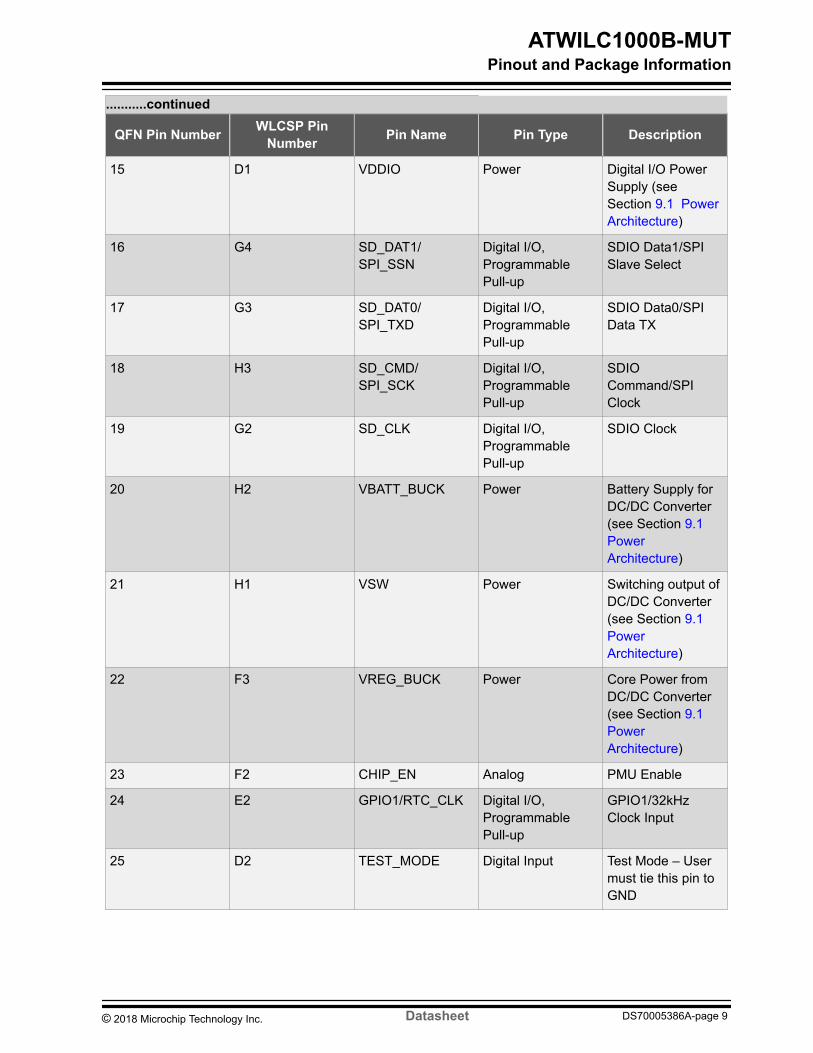
continued
QFN Pin Number WLCSP PinNumber Pin Name Pin Type Description
15 D1 VDDIO Power Digital IO PowerSupply (seeSection 91 PowerArchitecture)
16 G4 SD_DAT1SPI_SSN
Digital IOProgrammablePull-up
SDIO Data1SPISlave Select
17 G3 SD_DAT0SPI_TXD
Digital IOProgrammablePull-up
SDIO Data0SPIData TX
18 H3 SD_CMDSPI_SCK
Digital IOProgrammablePull-up
SDIOCommandSPIClock
19 G2 SD_CLK Digital IOProgrammablePull-up
SDIO Clock
20 H2 VBATT_BUCK Power Battery Supply forDCDC Converter(see Section 91 PowerArchitecture)
21 H1 VSW Power Switching output ofDCDC Converter(see Section 91 PowerArchitecture)
22 F3 VREG_BUCK Power Core Power fromDCDC Converter(see Section 91 PowerArchitecture)
23 F2 CHIP_EN Analog PMU Enable
24 E2 GPIO1RTC_CLK Digital IOProgrammablePull-up
GPIO132kHzClock Input
25 D2 TEST_MODE Digital Input Test Mode ndash Usermust tie this pin toGND
ATWILC1000B-MUTPinout and Package Information
copy 2018 Microchip Technology Inc Datasheet DS70005386A-page 9
continued
QFN Pin Number WLCSP PinNumber Pin Name Pin Type Description
26 H5 VDDIO Power Digital IO PowerSupply (seeSection 91 PowerArchitecture)
27 H6 VDDC Power Digital Core PowerSupply (seeSection 91 PowerArchitecture)
28 E3 GPIO3 Digital IOProgrammablePull-up
GPIO3SPI_SCK_Flash
29 D3 GPIO4 Digital IOProgrammablePull-up
GPIO4SPI_SSN_Flash
30 B2 GPIO5 Digital IOProgrammablePull-up
GPIO5SPI_TXD_Flash
31 A1 GPIO6 Digital IOProgrammablePull-up
GPIO6SPI_RXD_Flash
32 A2 I2C_SCL Digital IOProgrammablePull-up
I2C Slave Clock(high-drive padsee Table 4-3)
33 B3 I2C_SDA Digital IOProgrammablePull-up
I2C Slave Data(high-drive padsee Table 4-3)
34 A3 RESETN Digital Input Active-Low HardReset
35 A4 XO_N Analog Crystal Oscillator N
36 B4 XO_P Analog Crystal Oscillator P
37 A6 VDD_SXDIG Power SX Power Supply(see Section 91 PowerArchitecture)
38 - VDD_VCO Power VCO Power Supply(see Section 91 PowerArchitecture)
ATWILC1000B-MUTPinout and Package Information
copy 2018 Microchip Technology Inc Datasheet DS70005386A-page 10
continued
QFN Pin Number WLCSP PinNumber Pin Name Pin Type Description
39 A7 VDDIO_A Power Tuner VDDIOPower Supply (seeSection 91 PowerArchitecture)
40 B6 TP_N Analog Test PinNoConnect
41(1) - PADDLE VSS Ground Connect to SystemBoard Ground
- A5 GND_SXDIG Ground SX GroundConnect to SystemBoard Ground
- B1 GPIO16 Digital IOProgrammablePull-up
GPIO16
- B5 GND_IO Ground IO GroundConnect to SystemBoard Ground
- B8 NC None ReservedNoConnect
- C2 GPIO15 Digital IOProgrammablePull-up
GPIO15
- C3 GPIO17 Digital IOProgrammablePull-up
GPIO17
- C4 GPIO18 Digital IOProgrammablePull-up
GPIO18
- C5 GPIO13 Digital IOProgrammablePull-up
GPIO13
- C7 GND_RF_RX Ground RF Rx GroundConnect to SystemBoard Ground
- D8 GND_BATT_PPA Ground PA 2nd StageGround Connectto System BoardGround
ATWILC1000B-MUTPinout and Package Information
copy 2018 Microchip Technology Inc Datasheet DS70005386A-page 11
continued
QFN Pin Number WLCSP PinNumber Pin Name Pin Type Description
- E1 VSS Ground Connect to SystemBoard Ground
- E7 GND_BATT_PA Ground PA 1st StageGround Connectto System BoardGround
- F1 GND_BIAS Ground Bias GroundConnect to SystemBoard Ground
- F7 GND_AMS Ground AMS GroundConnect to SystemBoard Ground
- F8 TX_P Analog Positive RFDifferential IO
- G1 GND_BUCK Ground DCDC ConverterGround Connectto System BoardGround
- G6 GPIO12 Digital IOProgrammablePull-up
GPIO12
- G8 TX_N Analog Negative RFDifferential IO
- H4 VSS Ground Connect to SystemBoard Ground
- H7 GPIO11 Digital IOProgrammablePull-up
GPIO11
Note 1 Applies to QFN package only Pin 41 PADDLE_VSS must be soldered to GND providing good RF
grounding and good heat dissipation
ATWILC1000B-MUTPinout and Package Information
copy 2018 Microchip Technology Inc Datasheet DS70005386A-page 12
Figure 3-3 WLCSP ATWILC1000B UU
32 Package DescriptionThe ATWILC1000B QFN package information is provided in the following table and the package view isshown in Figure 3-4
Table 3-2 QFN Package Information
Parameter Value Unit Tolerance
Package size 5 x 5 mm plusmn01 mm
QFN pad count 40 ndash ndash
Total thickness 085 mm +015-005mm
QFN pad pitch 040 ndash
Pad width 020 ndash
Exposed pad size 37 x 37 ndash
The ATWILC1000B WLCSP package information is provided in the following table and the package viewis shown in the Figure 3-5
Table 3-3 WLCSP Package Information
Parameter Value Unit Tolerance
Package size 324 x 324
mm
plusmn03 mm
Total thickness 056 plusmn03 mm
IO Pitch 035 ndash
Ball diameter 020 plusmn03 mm
ATWILC1000B-MUTPinout and Package Information
copy 2018 Microchip Technology Inc Datasheet DS70005386A-page 13
Figure 3-4 QFN Package
Figure 3-5 WLCSP Package
ATWILC1000B-MUTPinout and Package Information
copy 2018 Microchip Technology Inc Datasheet DS70005386A-page 14
4 Electrical Specifications
41 Absolute RatingsThe values listed in this section are the peaked excursions ratings that can be tolerated by the deviceand if sustained will cause irreparable damage to the device
Table 4-1 Absolute Maximum Ratings
Characteristics Symbol Min Max Unit
Core supply voltage VDDC -03 15
V
IO supply voltage VDDIO -03 50
Battery supply voltage VBATT -03 50
Digital input voltage VIN (1) -03 VDDIO
Analog input voltage VAIN (2) -03 15
ESD human body model VESDHBM (3) -1000 -2000 (3) +1000 +2000 (3)
Storage temperature TA -65 150ordmC
Junction temperature ndash ndash 125
RF input power max ndash ndash 23 dBm
Note 1 VIN corresponds to all the digital pins2 VAIN corresponds to the following analog pins VDD_RF_RX VDD_RF_TX VDD_AMS RFIOP
RFION XO_N XO_P VDD_SXDIG and VDD_VCO3 For VESDHBM each pin is classified as Class 1 or Class 2 or both
ndash The Class 1 pins include all the pins (both analog and digital)ndash The Class 2 pins are all digital pins onlyndash VESDHBM is plusmn1 kV for Class 1 pins VESDHBM is plusmn2 kV for Class 2 pins
42 Recommended Operating ConditionsThe recommended operating conditions for the ATWILC1000B are listed in the following table
Table 4-2 Recommended Operating Conditions
Characteristics Symbol Min Typ Max Unit
IO supply voltage VDDIO 27 33 36V
Battery supply voltage VBATT 300 330 420
Operating temperature ndash -40 ndash 85 ordmC
ATWILC1000B-MUTElectrical Specifications
copy 2018 Microchip Technology Inc Datasheet DS70005386A-page 15
Note 1 The ATWILC1000B is functional across this range of voltages however optimal RF performance is
ensured for VBATT in the range 30V lt VBATT lt 42V2 IO supply voltage is applied to the VDDIO_A and VDDIO pins3 Battery supply voltage is applied to the VDD_BATT_PPA VDD_BATT_PA and VBATT_BUCK pins4 See Table 9-4 for the details of power connections
43 DC Electrical CharacteristicsThe following table provides the DC characteristics for the ATWILC1000B digital pads
Table 4-3 DC Electrical Characteristics
Characteristic Min Typ Max Unit
Input Low Voltage(VIL)
-030 ndash 060
V
Input High Voltage(VIH)
VDDIO-060 ndash VDDIO+030
Output LowVoltage (VOL)
ndash ndash 045
Output HighVoltage (OVOH)
VDDIO-050 ndash ndash
Output Loading ndash ndash 20pF
Digital Input Load ndash ndash 6
Pad Drive Strength(regular pads (1))
106 135 ndash
mAPad Drive Strength(high-drive pads (1))
212 27 ndash
Note 1 The following are high-drive pads I2C_SCL I2C_SDA all other pads are regular
ATWILC1000B-MUTElectrical Specifications
copy 2018 Microchip Technology Inc Datasheet DS70005386A-page 16
5 Clocking
51 Crystal OscillatorThe following table provides the crystal oscillator parameters of the ATWILC1000B
Table 5-1 Crystal Oscillator Parameters
Parameter Min Typ Max Unit
Crystal resonant frequency ndash 26 ndash MHz
Crystal equivalent series resistance ndash 50 150 Ω
Stability ndash Initial offset(1) -100 ndash 100ppm
Stability - Temperature and aging -25 ndash 25
Note 1 To ensure plusmn25 ppm under operating conditions frequency offset calibration is required
The following block diagram in figure XO Connections - (a) shows how the internal Crystal Oscillator(XO) is connected to the external crystal The XO has 5 pF internal capacitance (denoted as c_onchip inthe following figure) on each terminal XO_P and XO_N To bypass the crystal oscillator with an externalreference an external signal capable of driving 5 pF can be applied to the XO_N terminal as shown infollowing figure XO Connections - (b) The XO has 5 pF internal capacitance on each terminal XO_Pand XO_N This internal capacitance must be accounted for when calculating the external loadingcapacitance c_onboard for the XTAL
Figure 5-1 XO Connections (a) The Crystal Oscillator is Used (b) The Crystal Oscillator isBypassed
XO_N XO_P XO_N XO_P
External Clock
ATWILC1000 ATWILC1000
(a) (b)
c_onboard c_onboard
c_onchip c_onchip
The following table specifies the electrical and performance requirements for the external clock
ATWILC1000B-MUTClocking
copy 2018 Microchip Technology Inc Datasheet DS70005386A-page 17
Table 5-2 Bypass Clock Specification
Parameter Min Typ Max Unit Comments
Oscillationfrequency ndash 26 ndash MHz
Must drive 5 pFload at desiredfrequency
Voltage swing 05 ndash 12 VPPMust be ACcoupled
Stability ndashTemperatureand aging
-25ndash
+25 ppmndash
Phase noise ndash ndash -130 dBcHz At 10 kHz offset
Jitter (RMS) ndash ndash
lt1
psec Based onintegratedphase noisespectrum from1 kHz to 1 MHz
52 Low-Power OscillatorThe ATWILC1000B has an internally-generated 32 kHz clock to provide timing information for varioussleep functions Alternatively the ATWILC1000B allows for an external 32kHz clock to be used for thispurpose which is provided through pin 24 (RTC_CLK) Software selects whether the internal clock orexternal clock is used
The internal low-power clock is ring oscillator-based and has accuracy within 10000 ppm When usingthe internal low-power clock the advance wake-up time in the Beacon Monitoring mode has to beincreased by about 1 of the sleep time to compensate for the oscillator inaccuracy For example for theDTIM interval value of 1 wake-up time has to be increased by 1 ms
For any application targeting very low-power consumption an external 32 kHz RTC clock must be used
ATWILC1000B-MUTClocking
copy 2018 Microchip Technology Inc Datasheet DS70005386A-page 18
6 CPU and Memory Subsystem
61 ProcessorThe ATWILC1000B has a Cortus APS3 32-bit processor This processor performs many of the MACfunctions including but not limited to association authentication power management security keymanagement and MSDU aggregationde-aggregation In addition the processor provides flexibility forvarious modes of operation such as STA and AP modes
62 Memory SubsystemThe APS3 core uses a 128 KB instructionboot ROM along with a 160 KB instruction RAM and a 64 KBdata RAM In addition the device uses a 128 KB shared RAM accessible by the processor and MACwhich allows the APS3 core to perform various data management tasks on the TX and RX data packets
63 Nonvolatile Memory (eFuse)The ATWILC1000B has 768 bits of nonvolatile eFuse memory that can be read by the CPU after devicereset This nonvolatile One-Time-Programmable (OTP) memory can be used to store customer-specificparameters such as MAC address various calibration information such as TX power crystal frequencyoffset other software-specific configuration parameters and so on The eFuse is partitioned into six 128-bit banks Each bank has the same bit map which is shown in the following figure The purpose of thefirst 80 bits in each bank is fixed and the remaining 48 bits are general-purpose software dependent bitsor reserved for future use Since each bank can be programmed independently this allows for severalupdates of the device parameters following the initial programming eg updating the MAC addressRefer to the ATWILC1000 Programming Guide for the eFuse programming instructions
ATWILC1000B-MUTCPU and Memory Subsystem
copy 2018 Microchip Technology Inc Datasheet DS70005386A-page 19
Figure 6-1 eFuse Bit Map
Bank 0
Bank 1
Bank 2
Bank 3
Bank 4
Bank 5
F MAC ADDR
Used
Inva
lid
Version
Reserved
MACAD
DR
Used
FO
Flags
G
21 1 3 1
Use
d
TX Gain
Correct-
tion
Used
Freq
Offse
t
1 7
488 8 16
1 15
128 Bits
ATWILC1000B-MUTCPU and Memory Subsystem
copy 2018 Microchip Technology Inc Datasheet DS70005386A-page 20
7 WLAN SubsystemThe WLAN subsystem is composed of the Media Access Controller (MAC) and the Physical Layer (PHY)The following two subsections describe the MAC and PHY in detail
71 MAC
711 FeaturesThe ATWILC1000B IEEE80211 MAC supports the following functions
bull IEEE 80211bgnbull IEEE 80211e WMM QoS EDCAPCF Multiple Access Categories Traffic Schedulingbull Advanced IEEE 80211n Features
ndash Transmission and reception of aggregated MPDUs (A-MPDU)ndash Transmission and reception of aggregated MSDUs (A-MSDU)ndash Immediate Block Acknowledgmentndash Reduced Interframe Spacing (RIFS)
bull Support for IEEE 80211i and WFA Security with Key Managementndash WEP 64128ndash WPA-TKIPndash 128-bit WPA2 CCMP (AES)
bull Support for WAPI Securitybull Advanced Power Management
ndash Standard 80211 Power Save modendash Wi-Fi Alliancereg WMM-PS (U-APSD)
bull RTS-CTS and CTS-Self Supportbull Supports Either STA or AP Mode in the Infrastructure Basic Service Set Modebull Supports Independent Basic Service Set (IBSS)
712 DescriptionThe ATWILC1000B MAC is designed to operate at low power while providing high data throughput TheIEEE 80211 MAC functions are implemented with a combination of dedicated datapath engineshardwired control logic and a low-power high-efficiency microprocessor The combination of dedicatedlogic with a programmable processor provides optimal power efficiency and real-time response whileproviding the flexibility to accommodate evolving standards and future feature enhancements
Dedicated datapath engines with heavy computational are used to implement datapath functions Forexample an FCS engine checks the CRC of the transmitting and receiving packets and a cipher engineperforms all the required encryption and decryption operations for the WEP WPA-TKIP WPA2 CCMP-AES and WAPI security requirements
Control functions which have real-time requirements are implemented using hardwired control logicmodules These logic modules offer real-time response while maintaining configurability via theprocessor Examples of hardwired control logic modules are the channel access control module(implements EDCAHCCA Beacon TX control interframe spacing and so on) protocol timer module(responsible for the Network Access Vector back-off timing timing synchronization function and slotmanagement) MPDU handling module aggregationdeaggregation module block ACK controller
ATWILC1000B-MUTWLAN Subsystem
copy 2018 Microchip Technology Inc Datasheet DS70005386A-page 21
(implements the protocol requirements for burst block communication) and TXRX control FSMs(coordinate data movement between PHY-MAC interface cipher engine and the DMA interface to theTXRX FIFOs)
The MAC functions that are implemented in software on the microprocessor have the followingcharacteristics
bull Functions with high memory requirements or complex data structures Examples are associationtable management and power save queuing
bull Functions with low computational load or without critical real-time requirements Examples areauthentication and association
bull Functions which need flexibility and upgradeability Examples are beacon frame processing and QoSscheduling
72 PHY
721 FeaturesThe ATWILC1000B IEEE 80211 PHY supports the following functions
bull Single Antenna 1x1 Stream in 20 MHz Channelsbull Supports IEEE 80211b DSSS-CCK Modulation 1 2 55 and 11 Mbpsbull Supports IEEE 80211g OFDM Modulation 6 9 1218 24 36 48 and 54 Mbpsbull Supports IEEE 80211n HT Modulations MCS0-7 20 MHz 800 and 400 ns guard interval 65 72
130 144 195 217 260 289 390 433 520 578 585 650 and 722 Mbpsbull IEEE 80211n Mixed Mode Operationbull Per Packet TX Power Controlbull Advanced Channel EstimationEqualization Automatic Gain Control CCA CarrierSymbol Recovery
and Frame Detection
722 DescriptionThe ATWILC1000B WLAN PHY is designed to achieve reliable and power-efficient physical layercommunication specified by IEEE 80211 bgn in Single Stream mode with 20 MHz bandwidth Advancedalgorithms are used to achieve maximum throughput in a real-world communication environment withimpairments and interference The PHY implements all the required functions such as FFT filtering FEC(Viterbi decoder) frequency and timing acquisition and tracking channel estimation and equalizationcarrier sensing and clear channel assessment as well as the automatic gain control
73 RadioThis section describes the properties and characteristics of the ATWILC1000B and Wi-Fi radio transmitand receive performance capabilities of the device The performance measurements are taken at the RFpin assuming 50Ω impedance the RF performance is assured for room temperature of 25degC with aderating of 2-3dB at boundary conditions
Measurements were taken under typical conditions VBATT at 33V VDDIO at 33V and temperature at+25ordmC
ATWILC1000B-MUTWLAN Subsystem
copy 2018 Microchip Technology Inc Datasheet DS70005386A-page 22
Table 7-1 Features and Properties
Feature Description
Part Number ATWILC1000B
WLAN Standard IEEE 80211bgn Wi-Fi compliant
Host Interface SPI SDIO
Dimension L x W x H 217 x 147 x 21 (typical) mm
Frequency range 2412 GHz ~ 2472 GHz (24 GHz ISM band)
Number of channels 11 for North America 13 for Europe
Modulation 80211b DQPSK DBPSK CCK
80211gn OFDM64-QAM16-QAM QPSK BPSK
Data rate 80211b 1 2 55 11 Mbps80211g 6 9 12 18 24 36 48 54 Mbps
Data rate
(20 MHz short GI400ns)
80211n 72 144 217 289 433 578 65722Mbps
Operating temperature(1) -40degC to 85degC
Storage temperature -40degC to 125degC
Humidity Operating humidity 10 to 95 non-condensing
Storage humidity 5 to 95 non-condensing
Note 1 RF performance is ensured at room temperature of 25degC with a 2-3db change at boundary
conditions
731 Receiver PerformanceThe following are typical conditions for radio receiver performance
VBATT at 33V VDDIO at 33V temperature at 25degC and WLAN Channel 6 (2437 MHz)
The table below provides the receiver performance characteristics for the ATWILC1000B
Table 7-2 Receiver Performance
Parameter Description Min Typ Max Unit
Frequency - 2412 - 2472 MHz
Sensitivity 80211b 1 Mbps DSSS - -94 -
dBm2 Mbps DSSS - -91 -
55 Mbps DSSS - -89 -
11 Mbps DSSS - -86 -
ATWILC1000B-MUTWLAN Subsystem
copy 2018 Microchip Technology Inc Datasheet DS70005386A-page 23
continuedParameter Description Min Typ Max Unit
Sensitivity 80211g 6 Mbps OFDM - -88 -
dBm
9 Mbps OFDM - -87 -
12 Mbps OFDM - -86 -
18 Mbps OFDM - -84 -
24 Mbps OFDM - -82 -
36 Mbps OFDM - -78 -
48 Mbps OFDM - -74 -
54 Mbps OFDM - -73 -
Sensitivity 80211n (BW at 20 MHz) MCS 0 - -87 -
dBm
MCS 1 - -85 -
MCS 2 - -83 -
MCS 3 - -80 -
MCS 4 - -76 -
MCS 5 - -73 -
MCS 6 - -71 -
MCS 7 - -69 -
Maximum Receive Signal Level 1-11 Mbps DSSS - 0 -
dBm6-54 Mbps OFDM - -5 -
MCS 0 ndash 7 - -5 -
Adjacent Channel Rejection 1 Mbps DSSS (30 MHz offset) - 50 -
dB
11 Mbps DSSS (25 MHz offset) - 43 -
6 Mbps OFDM (25 MHz offset) - 40 -
54 Mbps OFDM (25 MHz offset) - 25 -
MCS 0 ndash 20 MHz BW (25 MHz offset) - 40 -
MCS 7 ndash 20 MHz BW (25 MHz offset) - 20 -
ATWILC1000B-MUTWLAN Subsystem
copy 2018 Microchip Technology Inc Datasheet DS70005386A-page 24
continuedParameter Description Min Typ Max Unit
Cellular Blocker Immunity 776-794 MHz CDMA - -14 -
dBm
824-849 MHz GSM - -10 -
880-915 MHz GSM - -10 -
1710-1785 MHz GSM - -15 -
1850-1910 MHz GSM - -15 -
1850-1910 MHz WCDMA - -24 -
1920-1980 MHz WCDMA - -24 -
732 Transmitter PerformanceThe following are typical conditions for radio transmitter performance
VBAT=33V VDDIO=33V temperature at 25degC and WLAN Channel 6 (2437 MHz)
The following table provides the transmitter performance characteristics for the ATWILC1000B
Table 7-3 Transmitter Performance
Parameter Description Min Typ Max Unit
Frequency - 2412 2472 MHz
Output power(1)-(2)ON_Transmit
80211b 1Mbps - 176 -
dBm
80211b 11Mbps - 182 -
80211g 6Mbps - 187 -
80211g 54Mbps - 167 -
80211n MCS 0 - 173 -
80211n MCS 7 - 138 -
TX power accuracy - - plusmn15 (2) dB
Carrier suppression 80211b mode - -194 -
dBc80211g mode - -275 -
80211n mode - -211 -
ATWILC1000B-MUTWLAN Subsystem
copy 2018 Microchip Technology Inc Datasheet DS70005386A-page 25
continuedParameter Description Min Typ Max Unit
Out of band Transmit Power 76-108 - -125 -
dBmHz
776-794 - -125 -
869-960 - -125 -
925-960 - -125 -
1570-1580 - -125 -
1805-1880 - -125 -
1930-1990 - -125 -
2110-2170 - -125 -
Harmonic output power(4) 2nd - -28 -
dBmMHz3rd - -33 -
4th - -40 -
5th - -28 -
Note 1 Measured at 80211 specification compliant EVMSpectral mask2 Measured after RF matching network3 Operating temperature range is -40ordmC to +85ordmC RF performance is ensured at a room temperature
range of 25ordmC with 2-3dB change at boundary conditions4 Measured at 11 Mbps DG (Digital Gain) = -7 WLAN Channel 6 (2437 MHz)5 With respect to TX power different (higherlower) RF output power settings may be used for
specific antennas andor enclosures in which case re-certification may be required6 The availability of some specific channels andor operational frequency bands are country
dependent and should be programmed at the host product factory to match the intendeddestination Regulatory bodies prohibit exposing the settings to the end user This requirementneeds to be taken care of via host implementation
ATWILC1000B-MUTWLAN Subsystem
copy 2018 Microchip Technology Inc Datasheet DS70005386A-page 26
8 External InterfacesThe ATWILC1000B external interfaces include
bull I2C slave for controlbull SPI slave and SDIO slave for control and data transferbull SPI master for external Flashbull I2C master for external EEPROMbull UART Debug Interfacebull General Purpose InputOutput (GPIO) pins
81 I2C Slave InterfaceThe I2C Slave interface used primarily for control by the host processor is a two-wire serial interfaceconsisting of a serial data line (SDA Pin 33) and a serial clock (SCL pin 32) It responds to the seven bitaddress value 0x60 The ATWILC1000B I2C supports I2C bus Version 21 - 2000 and can operate inStandard mode (with data rates up to 100 Kbs) and Fast mode (with data rates up to 400 Kbs) The I2CSlave is a synchronous serial interface The SDA line is a bidirectional signal and changes only while theSCL line is low except for STOP START and RESTART conditions The output drivers are open-drain toperform wire-AND functions on the bus The maximum number of devices on the bus is limited by onlythe maximum capacitance specification of 400 pF Data is transmitted in byte packages For specificinformation refer to the Philips Specification entitled ldquoThe I2C -Bus Specification Version 21rdquo The I2CSlave timing is provided in the following figure
Figure 8-1 I2C Slave Timing Diagram
tHL
SDA
SCL tHDSTA
tWL
tWH
tSUDAT tPR tHDDAT
tPR tPR
tLH tHL
tLH
tSUSTOtBUF
tSUSTAfSCL
The I2C Slave timing parameters are provided in the following table
Table 8-1 I2C Slave Timing Parameters
Parameter Symbol Min Max Unit Remarks
SCL clock frequency fSCL 0 400 kHz ndash
SCL low pulse width tWL 13 ndashmicros
ndash
SCL high pulse width tWH 06 ndash ndash
ATWILC1000B-MUTExternal Interfaces
copy 2018 Microchip Technology Inc Datasheet DS70005386A-page 27
continuedParameter Symbol Min Max Unit Remarks
SCL SDA fall time tHL ndash 300ns
ndash
SCL SDA rise time tLH ndash 300 This is dictated by externalcomponents
START setup time tSUSTA 06 ndashmicros
ndash
START hold time tHDSTA 06 ndash ndash
SDA setup time tSUDAT 100 ndash
ns
ndash
SDA hold time tHDDAT 0
40
ndash Slave and master default masterprogramming option
STOP setup time tSUSTO 06 ndashmicros
ndash
Bus free time between STOP and START tBUF 13 ndash ndash
Glitch pulse reject tPR 0 50 ns ndash
82 I2C Master InterfaceThe ATWILC1000B provides an I2C bus master which is intended primarily for accessing an externalEEPROM memory through a software-defined protocol The I2C Master is a two-wire serial interfaceconsisting of a serial data line (SDA) and a serial clock line (SCL) SDA can be configured on one of thefollowing pins SD_CLK (pin 19) GPIO1 (pin 24) GPIO6 (pin 31) or I2C_SDA (pin 33) SCL can beconfigured on one of the following pins GPIO0 (pin 10) SD_DAT3 (pin 12) GPIO4 (pin 29) or I2C_SCL(pin 32) For more specific instructions refer to the ATWILC1000 Programming Guide
The I2C master interface supports three speeds
bull Standard mode (100 kbs)bull Fast mode (400 kbs)bull High-Speed mode (34 Mbs)
The timing diagram of the I2C master interface is the same as that of the I2C slave interface (see Figure8-1) The timing parameters of I2C master are shown in the following table
Table 8-2 I2C Master Timing Parameters
Parameter Symbol Standard Mode Fast Mode High-Speed Mode Unit
Min Max Min Max Min Max
SCL clock frequency fSCL 0 100 0 400 0 3400 kHz
SCL high pulse width tWH 4 ndash 06 ndash 006 ndashmicros
SCL low pulse width tWL 47 ndash 13 ndash 016 ndash
ATWILC1000B-MUTExternal Interfaces
copy 2018 Microchip Technology Inc Datasheet DS70005386A-page 28
continuedParameter Symbol Standard Mode Fast Mode High-Speed Mode Unit
Min Max Min Max Min Max
SCL fall time tHLSCL ndash 300 ndash 300 10 40
nsSDA fall time tHLSDA ndash 300 300 10 80
SCL rise time tLHSCL ndash 1000 ndash 300 10 40
SDA rise time tLHSDA ndash 1000 ndash 300 10 80
START setup time tSUSTA 47 ndash 06 ndash 016 ndashmicros
START hold time tHDSTA 4 ndash 06 ndash 016 ndash
SDA setup time tSUDAT 250 ndash 100 ndash 10 ndashns
SDA hold time tHDDAT 5 ndash 40 ndash 0 70
STOP setup time tSUSTO 4 ndash 06 ndash 016 ndash
microsBus free time between STOP andSTART
tBUF 47 ndash 13 ndash ndash ndash
Glitch pulse reject tPR ndash ndash 0 50 ndash ndash
83 SPI Slave InterfaceThe ATWILC1000B provides a Serial Peripheral Interface (SPI) that operates as an SPI slave The SPISlave interface can be used for control and for serial IO of 80211 data The SPI Slave pins are mappedas shown in the the following table The RXD pin is same as Master Output Slave Input (MOSI) and theTXD pin is same as Master Input Slave Output (MISO) The SPI Slave is a full-duplex slave-synchronousserial interface that is available immediately following reset when pin 9 (SDIO_SPI_CFG) is tied toVDDIO
Table 8-3 SPI Slave Interface Pin Mapping
Pin Number SPI Function
9 CFG Must be tied to VDDIO
16 SSN Active Low Slave Select
18 SCK Serial Clock
13 RXD Serial Data Receive (MOSI)
17 TXD Serial Data Transmit (MISO)
When the SPI is not selected ie when SSN is high the SPI interface does not interfere with datatransfers between the serial-master and other serial-slave devices When the serial slave is not selectedits transmitted data output is buffered resulting in a high impedance drive onto the serial master receiveline
The SPI Slave interface responds to a protocol that allows an external host to read or write any register inthe chip as well as initiate DMA transfers For more details of the SPI protocol and more specificinstructions refer to the ATWILC1000 Programming Guide
ATWILC1000B-MUTExternal Interfaces
copy 2018 Microchip Technology Inc Datasheet DS70005386A-page 29
The SPI Slave interface supports four standard modes as determined by the Clock Polarity (CPOL) andClock Phase (CPHA) settings These modes are illustrated in table SPI Slave Modes and Figure 8-2 Thered lines in this figure correspond to Clock Phase = 0 and the blue lines correspond to Clock Phase = 1
Table 8-4 SPI Slave Modes
Mode CPOL CPHA
0 0 0
1 0 1
2 1 0
3 1 1
Figure 8-2 SPI Slave Clock Polarity and Clock Phase Timing
z
z z
z
SCKCPOL = 0
CPOL = 1
SSN
RXDTXD(MOSIMISO)
CPHA = 0
CPHA = 1
2 3 4 5 6 7 8
1 2 3 4 5 6 7
1
8
The SPI slave timing is provided in the following figure
ATWILC1000B-MUTExternal Interfaces
copy 2018 Microchip Technology Inc Datasheet DS70005386A-page 30
Figure 8-3 SPI Slave Timing Diagram
The SPI slave timing parameters are provided in the following table
Table 8-5 SPI Slave Timing Parameters
Parameter Symbol Min Max Unit
Clock input frequency fSCK ndash 48 MHz
Clock low pulse width tWL 15 ndash
ns
Clock high pulse width tWH 15 ndash
Clock rise time tLH ndash 10
Clock fall time tHL ndash 10
Input setup time tISU 5 ndash
Input hold time tIHD 5 ndash
Output delay tODLY 0 20
Slave select setup time tSUSSN 5 ndash
Slave select hold time tHDSSN 5 ndash
84 SPI Master InterfaceThe ATWILC1000B provides an SPI master interface for accessing external Flash memory The SPImaster pins are mapped as shown in the following table The TXD pin is same as Master Output SlaveInput (MOSI) and the RXD pin is same as Master Input Slave Output (MISO) The SPI master interfacesupports all four standard modes of clock polarity and clock phase shown in Table 8-4 External SPI Flash
ATWILC1000B-MUTExternal Interfaces
copy 2018 Microchip Technology Inc Datasheet DS70005386A-page 31
memory is accessed by a processor programming commands to the SPI master interface which in turninitiates a SPI master access to the Flash For more specific instructions refer to the ATWILC1000Programming Guide
Table 8-6 SPI Master Interface Pin Mapping
Pin Number Pin Name SPI Function
28 GPIO3 SCK Serial Clock Output
29 GPIO4 SCK Active-Low Slave Select Output
30 GPIO5 TXD Serial Data Transmit Output (MOSI)
31 GPIO6 RXD Serial Data Receive Input (MISO)
The SPI master timing is provided in the following figure
Figure 8-4 SPI Master Timing Diagram
fSCK
tWHtLH
tHL
tWL
tODLY tISU tIHD
SCK
SSNTXD
RXD
The SPI master timing parameters are provided in the following table
Table 8-7 SPI Master Timing Parameters
Parameter Symbol Min Max Unit
Clock output frequency fSCK ndash 48 MHz
Clock low pulse width tWL 5 ndash
ns
Clock high pulse width tWH 5 ndash
Clock rise time tLH ndash 5
Clock fall time tHL ndash 5
Input setup time tISU 5 ndash
Input hold time tIHD 5 ndash
Output delay tODLY 0 5
ATWILC1000B-MUTExternal Interfaces
copy 2018 Microchip Technology Inc Datasheet DS70005386A-page 32
85 SDIO Slave InterfaceThe ATWILC1000B SDIO Slave is a full speed interface The interface supports the 1-bit4-bit SDTransfer mode at the clock range of 0 to 50 MHz The host can use this interface to read and write fromany register within the chip as well as configure the ATWILC1000B for data DMA To use this interfacepin 9 (SDIO_SPI_CFG) must be grounded The SDIO slave pins are mapped as shown in the followingtable
Table 8-8 SDIO Interface Pin Mapping
Pin Number SPI Function
9 CFG Must be tied to ground
12 DAT3 Data 3
13 DAT2 Data 2
16 DAT1 Data 1
17 DAT0 Data 0
18 CMD Command
19 CLK Clock
When the SDIO card is inserted into an SDIO aware host the detection of the card will be via the meansdescribed in SDIO specification During the normal initialization and interrogation of the card by the hostthe card identifies itself as an SDIO device The host software obtains the card information in a tuple(linked list) format and determines if that cardrsquos IO function(s) are acceptable to activate If the card isacceptable it is allowed to power-up fully and start the IO function(s) built into it The SD memory cardcommunication is based on an advanced 9-pin interface (clock command four data and three powerlines) designed to operate at a maximum operating frequency of 50 MHz The SDIO slave interface hasthe following features
bull Meets SDIO card specification version 20bull Host clock rate variable between 0 to 50 MHzbull 1 bit4-bit SD bus modes supportedbull Allows card to interrupt hostbull Responds to direct readwrite (IO52) and extended readwrite (IO53) transactionsbull Supports SuspendResume operation
The SDIO slave interface timing is provided in the following figure
ATWILC1000B-MUTExternal Interfaces
copy 2018 Microchip Technology Inc Datasheet DS70005386A-page 33
Figure 8-5 SDIO Slave Timing Diagram
The SDIO slave timing parameters are provided in the following table
Table 8-9 SDIO Slave Timing Parameters
Parameter Symbol Min Max Unit
Clock input frequency fPP 0 50 MHz
Clock low pulse width tWL 10 ndash
ns
Clock high pulse width tWH 10 ndash
Clock rise time tLH ndash 10
Clock fall time tHL ndash 10
Input setup time tISU 5 ndash
Input hold time tIH 5 ndash
Output delay tODLY 0 14
86 UART Debug InterfaceATWILC1000B has a Universal Asynchronous ReceiverTransmitter (UART) interface on pin 13 SD-DATA2SPI-RxD and pin 17 SD-DATA0SPI-TXD This interface should be used only for debuggingpurposes The UART is compatible with the RS-232 standard where ATWILC1000B-MUT operates asData Terminal Equipment (DTE) It has a two-pin RXDTXD interface
The default configuration for accessing the UART interface of ATWILC1000B-MUT is as followsbull Baud rate 115200bull Data 8 bitbull Parity None
ATWILC1000B-MUTExternal Interfaces
copy 2018 Microchip Technology Inc Datasheet DS70005386A-page 34
bull Stop bit 1 bitbull Flow control None
It also has Rx and Tx FIFOs which ensures reliable high speed reception and low software overheadtransmission FIFO size is 4x8 for both Rx and Tx direction The UART has status registers that show thenumber of received characters available in the FIFO and various error conditions in addition it has theability to generate interrupts based on these status bits
An example of UART receiving or transmitting a single packet is shown in the following figure Thisexample shows 7-bit data (0x45) odd parity and two stop bits
Figure 8-6 Example of UART RX or TX Packet
87 GPIOsNine General Purpose InputOutput (GPIO) pins labeled GPIO 0-8 are available to allow for applicationspecific functions Each GPIO pin can be programmed as an input (the value of the pin can be read bythe host or internal processor) or as an output (the output values can be programmed by the host orinternal processor) where the default mode after power-up is input GPIOs 7 and 8 are only availablewhen the host does not use the SDIO interface which shares two of its pins with these GPIOs Thereforefor SDIO-based applications seven GPIOs (0-6) are available For more specific usage instructions referto the ATWILC1000 Programming Guide
ATWILC1000B-MUTExternal Interfaces
copy 2018 Microchip Technology Inc Datasheet DS70005386A-page 35
9 Power Management
91 Power ArchitectureThe ATWILC1000B uses an innovative power architecture to eliminate the need for external regulatorsand reduce the number of off-chip components This architecture is shown in the following figure ThePower Management Unit (PMU) has a DCDC Converter that converts VBATT to the core supply used bythe digital and RFAMS blocks The PA and eFuse are supplied by dedicated LDOs and the VCO issupplied by a separate LDO structure The power connections in the following figure provide a conceptualframework for understanding the ATWILC1000B power architecture
Figure 9-1 Power Architecture
VBATT _BUCKOff-Chip
LC
RFAMS Core
Sleep Osc RF
AM
S C
ore
Volta
ge
VSW
VREG_BUCK
VDD_AMS VDD_RF VDD_SXDIG
LDO1VDDIO_A VDD_VCO
LDO2
~VDD_BATT
12V
10V
CHIP_EN
EFuse LDO
SX
Digital Core
DCDC Converter
EFuse
PA
PMU
RFAMS
DigitalVDDC
Dig CoreLDO
25V
PadsVDDIO
SleepLDO
Digital Core Voltage
dcdc_ena
enaena
Vin Vout
enaena
The following table provides the typical values for the digital and RFAMS core voltages
ATWILC1000B-MUTPower Management
copy 2018 Microchip Technology Inc Datasheet DS70005386A-page 36
Table 9-1 PMU Output Voltages
Parameter Typical
RFAMS core voltage (VREG_BUCK) 135V
Digital core voltage (VDDC) 110V
Refer to the reference design for an example of power supply connections including proper isolation ofthe supplies used by the digital and RFAMS blocks
92 Power ConsumptionThe ATWILC1000B has several device states
bull ON_Transmit ndash Device is actively transmitting an 80211 signalbull ON_Receive ndash Device is actively receiving an 80211 signalbull ON_Doze ndash Device is on but is neither transmitting nor receivingbull Power_Down ndash Device core supply off (leakage)
The following pins are used to switch between the ON and Power_Down statesbull CHIP_EN ndash Device pin (pin 23) used to enable DCDC Converterbull VDDIO ndash IO supply voltage from external supply
In the ON states VDDIO is on and CHIP_EN is high (at VDDIO voltage level) To switch between the ONstates and Power_Down state CHIP_EN has to change between high and low (GND) voltage WhenVDDIO is off and CHIP_EN is low the chip is powered off with no leakage (also see 93 Power-UpDownSequence)
921 Current Consumption in Various Device StatesThe following table provides the ATWILC1000B current consumption in various device states
Table 9-2 Current Consumption
Device State Code Rate Output Power(dBm)
Current Consumption(1)
IVBATT IVDDIO
ON_Transmit 80211b 1 Mbps 176 266 mA 22 mA
80211b 11 Mbps 185 239 mA 22 mA
80211g 6 Mbps 186 249 mA 22 mA
80211g 54 Mbps 169 173 mA 22 mA
80211n MCS 0 177 253 mA 22 mA
80211n MCS 7 140 164 mA 22 mA
ATWILC1000B-MUTPower Management
copy 2018 Microchip Technology Inc Datasheet DS70005386A-page 37
continuedDevice State Code Rate Output Power
(dBm)Current Consumption(1)
IVBATT IVDDIO
ON_Receive 80211b 1 Mbps NA 63 mA 22 mA
80211b 11 Mbps NA 63 mA 22 mA
80211g 6 Mbps NA 63 mA 22 mA
80211g 54 Mbps NA 63 mA 22 mA
80211n MCS 0 NA 63 mA 22 mA
80211n MCS 7 NA 63 mA 22 mA
ON_Doze NA NA 380 microA lt10 microA
Power_Down NA NA 125 μA (2)
Note 1 The power consumption values are measured when VBAT is 36V and VDDIO is 28V at 25degC
922 Controlling the Device StatesTable Device States shows how to switch between the device states using the following
bull CHIP_EN ndash Device pin (pin 23) used to enable DCDC Converterbull VDDIO ndash IO supply voltage from external supply
Table 9-3 Device States
Device State CHIP_EN VDDIO Power Consumption (1) (2)
IVBATT IVDDIO
ON_Transmit VDDIO On 172mA 18dBm (le18Mbps)
230mA 18dBm (gt18Mbps)
2mA
ON_Receive VDDIO On 60mA 2mA
ON_Doze VDDIO ON 280μA lt10μA
Power_Down GND On lt05μA lt02μA
Note 1 Conditions VBAT 36v IO18V2 Power consumption numbers are preliminary
923 Restrictions for Power StatesWhen no power is supplied to the device ie the DCDC converter output and VDDIO are both off (atground potential) In this case a voltage cannot be applied to the device pins because each pin containsan ESD diode from the pin to supply This diode turns on when voltage higher than one diode-drop issupplied to the pin
If a voltage must be applied to the signal pads while the chip is in a low power state the VDDIO supplymust be on so the SLEEP or Power_Down state must be used
ATWILC1000B-MUTPower Management
copy 2018 Microchip Technology Inc Datasheet DS70005386A-page 38
Similarly to prevent the pin-to-ground diode from turning on do not apply a voltage that is more than onediode-drop below ground to any pin
93 Power-UpDown SequenceThe power-updown sequence for the ATWILC1000B is shown in the following figure
Figure 9-2 Power-UpDown Sequence
VBATT
VDDIO
CHIP_EN
RESETN
tBIO
t IOCE
tCER
XO Clock
The timing parameters are provided in the following table
Table 9-4 Power-UpDown Sequence Timing
Parameter Min Max Unit Description Notes
tA 0 ndash
ms
VBATT rise to VDDIOrise
VBATT and VDDIO can rise simultaneously orcan be tied together VDDIO must not risebefore VBATT
tB 0 ndash VDDIO rise toCHIP_EN rise
CHIP_EN must not rise before VDDIOCHIP_EN must be driven high or low not leftfloating
tC 5 ndash CHIP_EN rise toRESETN rise
This delay is needed because XO clock muststabilize before RESETN removal RESETNmust be driven high or low not left floating
tA 0 ndash VDDIO fall to VBATTfall
VBATT and VDDIO can fall simultaneously orcan be tied together VBATT must not fall beforeVDDIO
tB 0 ndash CHIP_EN fall to VDDIOfall
VDDIO must not fall before CHIP_ENCHIP_EN and RESETN can fall simultaneously
tC 0 ndash RESETN fall to VDDIOfall
VDDIO must not fall before RESETN RESETNand CHIP_EN can fall simultaneously
ATWILC1000B-MUTPower Management
copy 2018 Microchip Technology Inc Datasheet DS70005386A-page 39
94 Digital IO Pin Behavior During Power-up SequencesThe following table represents digital IO pin states corresponding to device power modes
Table 9-5 Digital IO Pin Behavior in Different Device States
Device State VDDIO CHIP_EN RESETN Output Driver InputDriver
Pull-UpDownResistor (96kΩ)
Power_Down
core supply off
High Low Low Disabled (Hi-Z) Disabled Disabled
Power-On Reset
core supply on hardreset on
High High Low Disabled (Hi-Z) Disabled Enabled
Power-On Default
core supply on deviceout of reset but notprogrammed yet
High High High Disabled (Hi-Z) Enabled Enabled
On_DozeOn_TransmitOn_Receive
core supply on deviceprogrammed byfirmware
High High High Programmed byfirmware for eachpin
Enabled orDisabled
Oppositeof outputdriver state
Programmed byfirmware foreach pin
Enabled orDisabled
ATWILC1000B-MUTPower Management
copy 2018 Microchip Technology Inc Datasheet DS70005386A-page 40
10 Reference DesignThe ATWILC1000B reference design schematic is shown in the following figure
Figure 10-1 ATWILC1000B Reference Schematic
47u
F
22u
H
Not
e1
Add
Tes
t poi
nts
for I
2C_S
CL
and
I2C
_SD
A pi
ns2
Add
Tes
t poi
nts
for U
ART
TxD
and
RxD
pin
s
22u
H
ATWILC1000B-MUTReference Design
copy 2018 Microchip Technology Inc Datasheet DS70005386A-page 41
11 Reflow Profile InformationThis section provides the guidelines for the reflow process to get ATWILC1000B soldered to thecustomers design
111 Storage Condition
1111 Moisture Barrier Bag Before OpeningA moisture barrier bag must be stored in a temperature of less than 30degC with humidity under 85 RHThe calculated shelf life for the dry-packed product shall be 12 months from the date the bag is sealed
1112 Moisture Barrier Bag OpenHumidity indicator cards must be blue indicating that the humidity is lt30
112 Solder PasteSnAgCu eutectic solder with melting temperature of 217degC is most commonly used for lead-free solderreflow application This alloy is widely accepted in the semiconductor industry due to its low costrelatively low melting temperature and good thermal fatigue resistance Some recommended pastesinclude NC-SMQreg 230 flux and Indalloyreg 241 solder paste made up of 955 Sn38 Ag07 Cu or SENJUN705-GRN3360-K2-V Type 3 no clean paste
113 Stencil DesignThe recommended stencil is laser-cut stainless-steel type with thickness of 100 microm to 130 microm andapproximately a 11 ratio of stencil opening to pad dimension To improve paste release a positive taperwith bottom opening 25 microm larger than the top is utilized Local manufacturing experience may find othercombinations of stencil thickness and aperture size to get good results
114 Printing ProcessThe printing process requires no significant changes compared to SnPb solder Any guidelinesrecommended by the paste manufacturers to accommodate paste specific characteristics should befollowed Post-print inspection and paste volume measurement is very critical to ensure good print qualityand uniform paste
115 Baking ConditionsATWILC1000B is rated at MSL level 3 After the sealed bag is opened no baking is required within 168hours as long as the devices are held at le 30degC60 RH or stored at lt 10 RH
ATWILC1000B requires baking before mounting ifbull The sealed bag has been open for more than 168 hoursbull The humidity indicator card reads more than 10bull SIPs need to be baked for eight hours at 125degC
ATWILC1000B-MUTReflow Profile Information
copy 2018 Microchip Technology Inc Datasheet DS70005386A-page 42
116 Soldering and Reflow ConditionOptimization of the reflow process is the most critical factor considered for lead-free soldering Thedevelopment of an optimal profile must account the paste characteristics the size of the board thedensity of the components the mix of the larger and smaller components and the peak temperaturerequirements of the components An optimized reflow process is the key to ensuring a successful lead-free assembly and achieves high yield and long-term solder joint reliability
Temperature ProfilingTemperature profiling must be performed for all new board designs by attaching thermocouples at thesolder joints on the top surface of the larger components and at multiple locations of the boards This isto ensure that all components are heated to a temperature above the minimum reflow temperatures andthe smaller components do not exceed the maximum temperature limit The SnAgCu solder alloy melts at~217degC so the reflow temperature peak at joint level must be 15 to 20degC higher than meltingtemperature The targeted solder joint temperature for the SnAgCu solder must be ~235degC For larger orsophisticated boards with a large mix of components it is also important to ensure that the temperaturedifference across the board is less than 10 degrees to minimize board warpage The maximumtemperature at the component body must not exceed the MSL3 qualification specification
1161 Reflow OvenIt is strongly recommended that a reflow oven equipped with more heating zones and Nitrogenatmosphere be used for lead-free assembly Nitrogen atmosphere has shown to improve the wet-abilityand reduce temperature gradient across the board It can also enhance the appearance of the solderjoints by reducing the effects of oxidation
The following items should also be observed in the reflow process1 Some recommended pastes include
ndash NC-SMQreg 230 flux and Indalloyreg 241 solder paste made up of 955 Sn38 Ag07 Cundash SENJU N705-GRN3360-K2-V Type 3 no clean paste
2 Allowable reflow soldering iterationsndash Three times based on the following reflow soldering profile (refer following Figure)
3 Temperature profilendash Reflow soldering shall be done according to the following temperature profile (refer to the
following figure)ndash Peak temperature 250degC
ATWILC1000B-MUTReflow Profile Information
copy 2018 Microchip Technology Inc Datasheet DS70005386A-page 43
Figure 11-1 Solder Reflow Profile
Cleaning
The exposed ground paddle helps to self-align ATWILC1000B avoiding pad misalignment The use ofno-clean solder pastes is recommended Full drying of no-clean paste fluxes must be ensured as a resultof the reflow process This may require longer reflow profiles andor peak temperatures toward the highend of the process window as recommended by the solder paste vendor It is believed that uncured fluxresidues could lead to corrosion andor shorting in accelerated testing and possibly the field
Rework
Rework is to remove the mounted SIP package and replace with a new unit It is recommended that onceATWILC1000B has been removed it should never be reused During the rework process the mountedATWILC1000B and PCB are heated partially and ATWILC1000B is removed It is recommended to heat-proof the proximity of the mounted parts and junctions and use the best nozzle for rework that is suited tothe module size
ATWILC1000B-MUTReflow Profile Information
copy 2018 Microchip Technology Inc Datasheet DS70005386A-page 44
12 Reference Documentation and SupportThe following table provides the set of collateral documents to ease integration and device ramp
Table 12-1 Reference Documents
Title Content
Design FilesPackage
User Guide Schematic PCB layout Gerber BOM and System notes on RFRadio Full Test Report radiation pattern design guidelines temperatureperformance ESD
Platform Gettingstarted Guide
How-to-use package Out of the Box starting guide HW limitations and notes SWQuick start guidelines
HW Design Guide Best practices and recommendations to design a board with the product includingAntenna Design for Wi-Fi (layout recommendations types of antennas impedancematching using a power amplifier etc) SPIUART protocol between Wi-Fi SoCand the Host MCU
SW Design Guide Integration guide with clear description of High level Arch overview on how towrite a networking application list all API parameters and structures
Features of the device SPIhandshake protocol between device and host MCUflowsequence state diagram and timing
SW ProgrammerGuide
Explains in detail the flow chart and how to use each API to implement all genericuse cases (eg start AP start STA provisioning UDP TCP http TLS p2p errorsmanagement connectiontransfer recovery mechanismstate diagram) ndash usageand sample application note
For a complete listing of development-support tools and documentation visit the ATWILC1000 webpageor refer to the customer support section on options to contact the nearest Microchip field representative
ATWILC1000B-MUTReference Documentation and Support
copy 2018 Microchip Technology Inc Datasheet DS70005386A-page 45
13 Document Revision HistoryRevision Date Section Description
A 122018 Document bull Updated from Atmelto Microchiptemplate
bull Assigned a newMicrochip documentnumber Previousversion is Atmel42351 revision D
bull ISBN numberadded
Document Revision History-Atmel
Doc Rev Date Comments
42351D 052015 DS update to Rev B offering
Changes from ATWILC1000A to ATWILC1000B
1 Added second UART increased UART data rates2 Increased instruction RAM size from 128KB to 160KB3 Updated pin MUX table added new options for various interfaces4 Improved description of Coexistence interface5 Added VDD_VCO switch and connection in the power architecture6 Updated power consumption numbers7 Updated reference schematic8 Changed RTC_CLK pad definition from pull-down to pull-up
42351C 022015 DS update new Atmel format
42351B 112014 Major document update new sections added replaced text in most sections newand updated drawings
42351A 072014 Initial document release
ATWILC1000B-MUTDocument Revision History
copy 2018 Microchip Technology Inc Datasheet DS70005386A-page 46
The Microchip Web Site
Microchip provides online support via our web site at httpwwwmicrochipcom This web site is used asa means to make files and information easily available to customers Accessible by using your favoriteInternet browser the web site contains the following information
bull Product Support ndash Data sheets and errata application notes and sample programs designresources userrsquos guides and hardware support documents latest software releases and archivedsoftware
bull General Technical Support ndash Frequently Asked Questions (FAQ) technical support requests onlinediscussion groups Microchip consultant program member listing
bull Business of Microchip ndash Product selector and ordering guides latest Microchip press releaseslisting of seminars and events listings of Microchip sales offices distributors and factoryrepresentatives
Customer Change Notification Service
Microchiprsquos customer notification service helps keep customers current on Microchip productsSubscribers will receive e-mail notification whenever there are changes updates revisions or erratarelated to a specified product family or development tool of interest
To register access the Microchip web site at httpwwwmicrochipcom Under ldquoSupportrdquo click onldquoCustomer Change Notificationrdquo and follow the registration instructions
Customer Support
Users of Microchip products can receive assistance through several channels
bull Distributor or Representativebull Local Sales Officebull Field Application Engineer (FAE)bull Technical Support
Customers should contact their distributor representative or Field Application Engineer (FAE) for supportLocal sales offices are also available to help customers A listing of sales offices and locations is includedin the back of this document
Technical support is available through the web site at httpwwwmicrochipcomsupport
Microchip Devices Code Protection Feature
Note the following details of the code protection feature on Microchip devices
bull Microchip products meet the specification contained in their particular Microchip Data Sheetbull Microchip believes that its family of products is one of the most secure families of its kind on the
market today when used in the intended manner and under normal conditionsbull There are dishonest and possibly illegal methods used to breach the code protection feature All of
these methods to our knowledge require using the Microchip products in a manner outside theoperating specifications contained in Microchiprsquos Data Sheets Most likely the person doing so isengaged in theft of intellectual property
bull Microchip is willing to work with the customer who is concerned about the integrity of their code
ATWILC1000B-MUT
copy 2018 Microchip Technology Inc Datasheet DS70005386A-page 47
bull Neither Microchip nor any other semiconductor manufacturer can guarantee the security of theircode Code protection does not mean that we are guaranteeing the product as ldquounbreakablerdquo
Code protection is constantly evolving We at Microchip are committed to continuously improving thecode protection features of our products Attempts to break Microchiprsquos code protection feature may be aviolation of the Digital Millennium Copyright Act If such acts allow unauthorized access to your softwareor other copyrighted work you may have a right to sue for relief under that Act
Legal Notice
Information contained in this publication regarding device applications and the like is provided only foryour convenience and may be superseded by updates It is your responsibility to ensure that yourapplication meets with your specifications MICROCHIP MAKES NO REPRESENTATIONS ORWARRANTIES OF ANY KIND WHETHER EXPRESS OR IMPLIED WRITTEN OR ORAL STATUTORYOR OTHERWISE RELATED TO THE INFORMATION INCLUDING BUT NOT LIMITED TO ITSCONDITION QUALITY PERFORMANCE MERCHANTABILITY OR FITNESS FOR PURPOSEMicrochip disclaims all liability arising from this information and its use Use of Microchip devices in lifesupport andor safety applications is entirely at the buyerrsquos risk and the buyer agrees to defendindemnify and hold harmless Microchip from any and all damages claims suits or expenses resultingfrom such use No licenses are conveyed implicitly or otherwise under any Microchip intellectualproperty rights unless otherwise stated
Trademarks
The Microchip name and logo the Microchip logo AnyRate AVR AVR logo AVR Freaks BitCloudchipKIT chipKIT logo CryptoMemory CryptoRF dsPIC FlashFlex flexPWR Heldo JukeBlox KeeLoqKleer LANCheck LINK MD maXStylus maXTouch MediaLB megaAVR MOST MOST logo MPLABOptoLyzer PIC picoPower PICSTART PIC32 logo Prochip Designer QTouch SAM-BA SpyNIC SSTSST Logo SuperFlash tinyAVR UNIO and XMEGA are registered trademarks of Microchip TechnologyIncorporated in the USA and other countries
ClockWorks The Embedded Control Solutions Company EtherSynch Hyper Speed Control HyperLightLoad IntelliMOS mTouch Precision Edge and Quiet-Wire are registered trademarks of MicrochipTechnology Incorporated in the USA
Adjacent Key Suppression AKS Analog-for-the-Digital Age Any Capacitor AnyIn AnyOut BodyComCodeGuard CryptoAuthentication CryptoAutomotive CryptoCompanion CryptoController dsPICDEMdsPICDEMnet Dynamic Average Matching DAM ECAN EtherGREEN In-Circuit Serial ProgrammingICSP INICnet Inter-Chip Connectivity JitterBlocker KleerNet KleerNet logo memBrain Mindi MiWimotorBench MPASM MPF MPLAB Certified logo MPLIB MPLINK MultiTRAK NetDetach OmniscientCode Generation PICDEM PICDEMnet PICkit PICtail PowerSmart PureSilicon QMatrix REAL ICERipple Blocker SAM-ICE Serial Quad IO SMART-IS SQI SuperSwitcher SuperSwitcher II TotalEndurance TSHARC USBCheck VariSense ViewSpan WiperLock Wireless DNA and ZENA aretrademarks of Microchip Technology Incorporated in the USA and other countries
SQTP is a service mark of Microchip Technology Incorporated in the USA
Silicon Storage Technology is a registered trademark of Microchip Technology Inc in other countries
GestIC is a registered trademark of Microchip Technology Germany II GmbH amp Co KG a subsidiary ofMicrochip Technology Inc in other countries
All other trademarks mentioned herein are property of their respective companies
ATWILC1000B-MUT
copy 2018 Microchip Technology Inc Datasheet DS70005386A-page 48
copy 2018 Microchip Technology Incorporated Printed in the USA All Rights Reserved
ISBN 978-1-5224-3998-1
Quality Management System Certified by DNV
ISOTS 16949Microchip received ISOTS-169492009 certification for its worldwide headquarters design and waferfabrication facilities in Chandler and Tempe Arizona Gresham Oregon and design centers in Californiaand India The Companyrsquos quality system processes and procedures are for its PICreg MCUs and dsPICreg
DSCs KEELOQreg code hopping devices Serial EEPROMs microperipherals nonvolatile memory andanalog products In addition Microchiprsquos quality system for the design and manufacture of developmentsystems is ISO 90012000 certified
ATWILC1000B-MUT
copy 2018 Microchip Technology Inc Datasheet DS70005386A-page 49
AMERICAS ASIAPACIFIC ASIAPACIFIC EUROPECorporate Office2355 West Chandler BlvdChandler AZ 85224-6199Tel 480-792-7200Fax 480-792-7277Technical SupporthttpwwwmicrochipcomsupportWeb AddresswwwmicrochipcomAtlantaDuluth GATel 678-957-9614Fax 678-957-1455Austin TXTel 512-257-3370BostonWestborough MATel 774-760-0087Fax 774-760-0088ChicagoItasca ILTel 630-285-0071Fax 630-285-0075DallasAddison TXTel 972-818-7423Fax 972-818-2924DetroitNovi MITel 248-848-4000Houston TXTel 281-894-5983IndianapolisNoblesville INTel 317-773-8323Fax 317-773-5453Tel 317-536-2380Los AngelesMission Viejo CATel 949-462-9523Fax 949-462-9608Tel 951-273-7800Raleigh NCTel 919-844-7510New York NYTel 631-435-6000San Jose CATel 408-735-9110Tel 408-436-4270Canada - TorontoTel 905-695-1980Fax 905-695-2078
Australia - SydneyTel 61-2-9868-6733China - BeijingTel 86-10-8569-7000China - ChengduTel 86-28-8665-5511China - ChongqingTel 86-23-8980-9588China - DongguanTel 86-769-8702-9880China - GuangzhouTel 86-20-8755-8029China - HangzhouTel 86-571-8792-8115China - Hong Kong SARTel 852-2943-5100China - NanjingTel 86-25-8473-2460China - QingdaoTel 86-532-8502-7355China - ShanghaiTel 86-21-3326-8000China - ShenyangTel 86-24-2334-2829China - ShenzhenTel 86-755-8864-2200China - SuzhouTel 86-186-6233-1526China - WuhanTel 86-27-5980-5300China - XianTel 86-29-8833-7252China - XiamenTel 86-592-2388138China - ZhuhaiTel 86-756-3210040
India - BangaloreTel 91-80-3090-4444India - New DelhiTel 91-11-4160-8631India - PuneTel 91-20-4121-0141Japan - OsakaTel 81-6-6152-7160Japan - TokyoTel 81-3-6880- 3770Korea - DaeguTel 82-53-744-4301Korea - SeoulTel 82-2-554-7200Malaysia - Kuala LumpurTel 60-3-7651-7906Malaysia - PenangTel 60-4-227-8870Philippines - ManilaTel 63-2-634-9065SingaporeTel 65-6334-8870Taiwan - Hsin ChuTel 886-3-577-8366Taiwan - KaohsiungTel 886-7-213-7830Taiwan - TaipeiTel 886-2-2508-8600Thailand - BangkokTel 66-2-694-1351Vietnam - Ho Chi MinhTel 84-28-5448-2100
Austria - WelsTel 43-7242-2244-39Fax 43-7242-2244-393Denmark - CopenhagenTel 45-4450-2828Fax 45-4485-2829Finland - EspooTel 358-9-4520-820France - ParisTel 33-1-69-53-63-20Fax 33-1-69-30-90-79Germany - GarchingTel 49-8931-9700Germany - HaanTel 49-2129-3766400Germany - HeilbronnTel 49-7131-67-3636Germany - KarlsruheTel 49-721-625370Germany - MunichTel 49-89-627-144-0Fax 49-89-627-144-44Germany - RosenheimTel 49-8031-354-560Israel - RarsquoananaTel 972-9-744-7705Italy - MilanTel 39-0331-742611Fax 39-0331-466781Italy - PadovaTel 39-049-7625286Netherlands - DrunenTel 31-416-690399Fax 31-416-690340Norway - TrondheimTel 47-72884388Poland - WarsawTel 48-22-3325737Romania - BucharestTel 40-21-407-87-50Spain - MadridTel 34-91-708-08-90Fax 34-91-708-08-91Sweden - GothenbergTel 46-31-704-60-40Sweden - StockholmTel 46-8-5090-4654UK - WokinghamTel 44-118-921-5800Fax 44-118-921-5820
Worldwide Sales and Service
copy 2018 Microchip Technology Inc Datasheet DS70005386A-page 50
- Introduction
- Features
- Table of Contents
- 1 Ordering Information and IC Marking
- 2 Block Diagram
- 3 Pinout and Package Information
-
- 31 Pin Description
- 32 Package Description
-
- 4 Electrical Specifications
-
- 41 Absolute Ratings
- 42 Recommended Operating Conditions
- 43 DC Electrical Characteristics
-
- 5 Clocking
-
- 51 Crystal Oscillator
- 52 Low-Power Oscillator
-
- 6 CPU and Memory Subsystem
-
- 61 Processor
- 62 Memory Subsystem
- 63 Nonvolatile Memory (eFuse)
-
- 7 WLAN Subsystem
-
- 71 MAC
-
- 711 Features
- 712 Description
-
- 72 PHY
-
- 721 Features
- 722 Description
-
- 73 Radio
-
- 731 Receiver Performance
- 732 Transmitter Performance
-
- 8 External Interfaces
-
- 81 I2C Slave Interface
- 82 I2C Master Interface
- 83 SPI Slave Interface
- 84 SPI Master Interface
- 85 SDIO Slave Interface
- 86 UART Debug Interface
- 87 GPIOs
-
- 9 Power Management
-
- 91 Power Architecture
- 92 Power Consumption
-
- 921 Current Consumption in Various Device States
- 922 Controlling the Device States
- 923 Restrictions for Power States
-
- 93 Power-UpDown Sequence
- 94 Digital IO Pin Behavior During Power-up Sequences
-
- 10 Reference Design
- 11 Reflow Profile Information
-
- 111 Storage Condition
-
- 1111 Moisture Barrier Bag Before Opening
- 1112 Moisture Barrier Bag Open
-
- 112 Solder Paste
- 113 Stencil Design
- 114 Printing Process
- 115 Baking Conditions
- 116 Soldering and Reflow Condition
-
- 1161 Reflow Oven
-
- 12 Reference Documentation and Support
- 13 Document Revision History
- The Microchip Web Site
- Customer Change Notification Service
- Customer Support
- Microchip Devices Code Protection Feature
- Legal Notice
- Trademarks
- Quality Management System Certified by DNV
- Worldwide Sales and Service
-
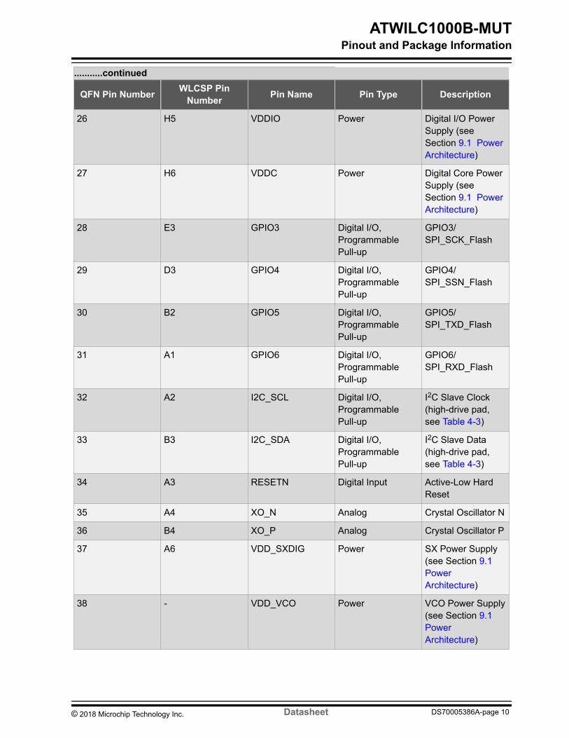
continued
QFN Pin Number WLCSP PinNumber Pin Name Pin Type Description
26 H5 VDDIO Power Digital IO PowerSupply (seeSection 91 PowerArchitecture)
27 H6 VDDC Power Digital Core PowerSupply (seeSection 91 PowerArchitecture)
28 E3 GPIO3 Digital IOProgrammablePull-up
GPIO3SPI_SCK_Flash
29 D3 GPIO4 Digital IOProgrammablePull-up
GPIO4SPI_SSN_Flash
30 B2 GPIO5 Digital IOProgrammablePull-up
GPIO5SPI_TXD_Flash
31 A1 GPIO6 Digital IOProgrammablePull-up
GPIO6SPI_RXD_Flash
32 A2 I2C_SCL Digital IOProgrammablePull-up
I2C Slave Clock(high-drive padsee Table 4-3)
33 B3 I2C_SDA Digital IOProgrammablePull-up
I2C Slave Data(high-drive padsee Table 4-3)
34 A3 RESETN Digital Input Active-Low HardReset
35 A4 XO_N Analog Crystal Oscillator N
36 B4 XO_P Analog Crystal Oscillator P
37 A6 VDD_SXDIG Power SX Power Supply(see Section 91 PowerArchitecture)
38 - VDD_VCO Power VCO Power Supply(see Section 91 PowerArchitecture)
ATWILC1000B-MUTPinout and Package Information
copy 2018 Microchip Technology Inc Datasheet DS70005386A-page 10
continued
QFN Pin Number WLCSP PinNumber Pin Name Pin Type Description
39 A7 VDDIO_A Power Tuner VDDIOPower Supply (seeSection 91 PowerArchitecture)
40 B6 TP_N Analog Test PinNoConnect
41(1) - PADDLE VSS Ground Connect to SystemBoard Ground
- A5 GND_SXDIG Ground SX GroundConnect to SystemBoard Ground
- B1 GPIO16 Digital IOProgrammablePull-up
GPIO16
- B5 GND_IO Ground IO GroundConnect to SystemBoard Ground
- B8 NC None ReservedNoConnect
- C2 GPIO15 Digital IOProgrammablePull-up
GPIO15
- C3 GPIO17 Digital IOProgrammablePull-up
GPIO17
- C4 GPIO18 Digital IOProgrammablePull-up
GPIO18
- C5 GPIO13 Digital IOProgrammablePull-up
GPIO13
- C7 GND_RF_RX Ground RF Rx GroundConnect to SystemBoard Ground
- D8 GND_BATT_PPA Ground PA 2nd StageGround Connectto System BoardGround
ATWILC1000B-MUTPinout and Package Information
copy 2018 Microchip Technology Inc Datasheet DS70005386A-page 11
continued
QFN Pin Number WLCSP PinNumber Pin Name Pin Type Description
- E1 VSS Ground Connect to SystemBoard Ground
- E7 GND_BATT_PA Ground PA 1st StageGround Connectto System BoardGround
- F1 GND_BIAS Ground Bias GroundConnect to SystemBoard Ground
- F7 GND_AMS Ground AMS GroundConnect to SystemBoard Ground
- F8 TX_P Analog Positive RFDifferential IO
- G1 GND_BUCK Ground DCDC ConverterGround Connectto System BoardGround
- G6 GPIO12 Digital IOProgrammablePull-up
GPIO12
- G8 TX_N Analog Negative RFDifferential IO
- H4 VSS Ground Connect to SystemBoard Ground
- H7 GPIO11 Digital IOProgrammablePull-up
GPIO11
Note 1 Applies to QFN package only Pin 41 PADDLE_VSS must be soldered to GND providing good RF
grounding and good heat dissipation
ATWILC1000B-MUTPinout and Package Information
copy 2018 Microchip Technology Inc Datasheet DS70005386A-page 12
Figure 3-3 WLCSP ATWILC1000B UU
32 Package DescriptionThe ATWILC1000B QFN package information is provided in the following table and the package view isshown in Figure 3-4
Table 3-2 QFN Package Information
Parameter Value Unit Tolerance
Package size 5 x 5 mm plusmn01 mm
QFN pad count 40 ndash ndash
Total thickness 085 mm +015-005mm
QFN pad pitch 040 ndash
Pad width 020 ndash
Exposed pad size 37 x 37 ndash
The ATWILC1000B WLCSP package information is provided in the following table and the package viewis shown in the Figure 3-5
Table 3-3 WLCSP Package Information
Parameter Value Unit Tolerance
Package size 324 x 324
mm
plusmn03 mm
Total thickness 056 plusmn03 mm
IO Pitch 035 ndash
Ball diameter 020 plusmn03 mm
ATWILC1000B-MUTPinout and Package Information
copy 2018 Microchip Technology Inc Datasheet DS70005386A-page 13
Figure 3-4 QFN Package
Figure 3-5 WLCSP Package
ATWILC1000B-MUTPinout and Package Information
copy 2018 Microchip Technology Inc Datasheet DS70005386A-page 14
4 Electrical Specifications
41 Absolute RatingsThe values listed in this section are the peaked excursions ratings that can be tolerated by the deviceand if sustained will cause irreparable damage to the device
Table 4-1 Absolute Maximum Ratings
Characteristics Symbol Min Max Unit
Core supply voltage VDDC -03 15
V
IO supply voltage VDDIO -03 50
Battery supply voltage VBATT -03 50
Digital input voltage VIN (1) -03 VDDIO
Analog input voltage VAIN (2) -03 15
ESD human body model VESDHBM (3) -1000 -2000 (3) +1000 +2000 (3)
Storage temperature TA -65 150ordmC
Junction temperature ndash ndash 125
RF input power max ndash ndash 23 dBm
Note 1 VIN corresponds to all the digital pins2 VAIN corresponds to the following analog pins VDD_RF_RX VDD_RF_TX VDD_AMS RFIOP
RFION XO_N XO_P VDD_SXDIG and VDD_VCO3 For VESDHBM each pin is classified as Class 1 or Class 2 or both
ndash The Class 1 pins include all the pins (both analog and digital)ndash The Class 2 pins are all digital pins onlyndash VESDHBM is plusmn1 kV for Class 1 pins VESDHBM is plusmn2 kV for Class 2 pins
42 Recommended Operating ConditionsThe recommended operating conditions for the ATWILC1000B are listed in the following table
Table 4-2 Recommended Operating Conditions
Characteristics Symbol Min Typ Max Unit
IO supply voltage VDDIO 27 33 36V
Battery supply voltage VBATT 300 330 420
Operating temperature ndash -40 ndash 85 ordmC
ATWILC1000B-MUTElectrical Specifications
copy 2018 Microchip Technology Inc Datasheet DS70005386A-page 15
Note 1 The ATWILC1000B is functional across this range of voltages however optimal RF performance is
ensured for VBATT in the range 30V lt VBATT lt 42V2 IO supply voltage is applied to the VDDIO_A and VDDIO pins3 Battery supply voltage is applied to the VDD_BATT_PPA VDD_BATT_PA and VBATT_BUCK pins4 See Table 9-4 for the details of power connections
43 DC Electrical CharacteristicsThe following table provides the DC characteristics for the ATWILC1000B digital pads
Table 4-3 DC Electrical Characteristics
Characteristic Min Typ Max Unit
Input Low Voltage(VIL)
-030 ndash 060
V
Input High Voltage(VIH)
VDDIO-060 ndash VDDIO+030
Output LowVoltage (VOL)
ndash ndash 045
Output HighVoltage (OVOH)
VDDIO-050 ndash ndash
Output Loading ndash ndash 20pF
Digital Input Load ndash ndash 6
Pad Drive Strength(regular pads (1))
106 135 ndash
mAPad Drive Strength(high-drive pads (1))
212 27 ndash
Note 1 The following are high-drive pads I2C_SCL I2C_SDA all other pads are regular
ATWILC1000B-MUTElectrical Specifications
copy 2018 Microchip Technology Inc Datasheet DS70005386A-page 16
5 Clocking
51 Crystal OscillatorThe following table provides the crystal oscillator parameters of the ATWILC1000B
Table 5-1 Crystal Oscillator Parameters
Parameter Min Typ Max Unit
Crystal resonant frequency ndash 26 ndash MHz
Crystal equivalent series resistance ndash 50 150 Ω
Stability ndash Initial offset(1) -100 ndash 100ppm
Stability - Temperature and aging -25 ndash 25
Note 1 To ensure plusmn25 ppm under operating conditions frequency offset calibration is required
The following block diagram in figure XO Connections - (a) shows how the internal Crystal Oscillator(XO) is connected to the external crystal The XO has 5 pF internal capacitance (denoted as c_onchip inthe following figure) on each terminal XO_P and XO_N To bypass the crystal oscillator with an externalreference an external signal capable of driving 5 pF can be applied to the XO_N terminal as shown infollowing figure XO Connections - (b) The XO has 5 pF internal capacitance on each terminal XO_Pand XO_N This internal capacitance must be accounted for when calculating the external loadingcapacitance c_onboard for the XTAL
Figure 5-1 XO Connections (a) The Crystal Oscillator is Used (b) The Crystal Oscillator isBypassed
XO_N XO_P XO_N XO_P
External Clock
ATWILC1000 ATWILC1000
(a) (b)
c_onboard c_onboard
c_onchip c_onchip
The following table specifies the electrical and performance requirements for the external clock
ATWILC1000B-MUTClocking
copy 2018 Microchip Technology Inc Datasheet DS70005386A-page 17
Table 5-2 Bypass Clock Specification
Parameter Min Typ Max Unit Comments
Oscillationfrequency ndash 26 ndash MHz
Must drive 5 pFload at desiredfrequency
Voltage swing 05 ndash 12 VPPMust be ACcoupled
Stability ndashTemperatureand aging
-25ndash
+25 ppmndash
Phase noise ndash ndash -130 dBcHz At 10 kHz offset
Jitter (RMS) ndash ndash
lt1
psec Based onintegratedphase noisespectrum from1 kHz to 1 MHz
52 Low-Power OscillatorThe ATWILC1000B has an internally-generated 32 kHz clock to provide timing information for varioussleep functions Alternatively the ATWILC1000B allows for an external 32kHz clock to be used for thispurpose which is provided through pin 24 (RTC_CLK) Software selects whether the internal clock orexternal clock is used
The internal low-power clock is ring oscillator-based and has accuracy within 10000 ppm When usingthe internal low-power clock the advance wake-up time in the Beacon Monitoring mode has to beincreased by about 1 of the sleep time to compensate for the oscillator inaccuracy For example for theDTIM interval value of 1 wake-up time has to be increased by 1 ms
For any application targeting very low-power consumption an external 32 kHz RTC clock must be used
ATWILC1000B-MUTClocking
copy 2018 Microchip Technology Inc Datasheet DS70005386A-page 18
6 CPU and Memory Subsystem
61 ProcessorThe ATWILC1000B has a Cortus APS3 32-bit processor This processor performs many of the MACfunctions including but not limited to association authentication power management security keymanagement and MSDU aggregationde-aggregation In addition the processor provides flexibility forvarious modes of operation such as STA and AP modes
62 Memory SubsystemThe APS3 core uses a 128 KB instructionboot ROM along with a 160 KB instruction RAM and a 64 KBdata RAM In addition the device uses a 128 KB shared RAM accessible by the processor and MACwhich allows the APS3 core to perform various data management tasks on the TX and RX data packets
63 Nonvolatile Memory (eFuse)The ATWILC1000B has 768 bits of nonvolatile eFuse memory that can be read by the CPU after devicereset This nonvolatile One-Time-Programmable (OTP) memory can be used to store customer-specificparameters such as MAC address various calibration information such as TX power crystal frequencyoffset other software-specific configuration parameters and so on The eFuse is partitioned into six 128-bit banks Each bank has the same bit map which is shown in the following figure The purpose of thefirst 80 bits in each bank is fixed and the remaining 48 bits are general-purpose software dependent bitsor reserved for future use Since each bank can be programmed independently this allows for severalupdates of the device parameters following the initial programming eg updating the MAC addressRefer to the ATWILC1000 Programming Guide for the eFuse programming instructions
ATWILC1000B-MUTCPU and Memory Subsystem
copy 2018 Microchip Technology Inc Datasheet DS70005386A-page 19
Figure 6-1 eFuse Bit Map
Bank 0
Bank 1
Bank 2
Bank 3
Bank 4
Bank 5
F MAC ADDR
Used
Inva
lid
Version
Reserved
MACAD
DR
Used
FO
Flags
G
21 1 3 1
Use
d
TX Gain
Correct-
tion
Used
Freq
Offse
t
1 7
488 8 16
1 15
128 Bits
ATWILC1000B-MUTCPU and Memory Subsystem
copy 2018 Microchip Technology Inc Datasheet DS70005386A-page 20
7 WLAN SubsystemThe WLAN subsystem is composed of the Media Access Controller (MAC) and the Physical Layer (PHY)The following two subsections describe the MAC and PHY in detail
71 MAC
711 FeaturesThe ATWILC1000B IEEE80211 MAC supports the following functions
bull IEEE 80211bgnbull IEEE 80211e WMM QoS EDCAPCF Multiple Access Categories Traffic Schedulingbull Advanced IEEE 80211n Features
ndash Transmission and reception of aggregated MPDUs (A-MPDU)ndash Transmission and reception of aggregated MSDUs (A-MSDU)ndash Immediate Block Acknowledgmentndash Reduced Interframe Spacing (RIFS)
bull Support for IEEE 80211i and WFA Security with Key Managementndash WEP 64128ndash WPA-TKIPndash 128-bit WPA2 CCMP (AES)
bull Support for WAPI Securitybull Advanced Power Management
ndash Standard 80211 Power Save modendash Wi-Fi Alliancereg WMM-PS (U-APSD)
bull RTS-CTS and CTS-Self Supportbull Supports Either STA or AP Mode in the Infrastructure Basic Service Set Modebull Supports Independent Basic Service Set (IBSS)
712 DescriptionThe ATWILC1000B MAC is designed to operate at low power while providing high data throughput TheIEEE 80211 MAC functions are implemented with a combination of dedicated datapath engineshardwired control logic and a low-power high-efficiency microprocessor The combination of dedicatedlogic with a programmable processor provides optimal power efficiency and real-time response whileproviding the flexibility to accommodate evolving standards and future feature enhancements
Dedicated datapath engines with heavy computational are used to implement datapath functions Forexample an FCS engine checks the CRC of the transmitting and receiving packets and a cipher engineperforms all the required encryption and decryption operations for the WEP WPA-TKIP WPA2 CCMP-AES and WAPI security requirements
Control functions which have real-time requirements are implemented using hardwired control logicmodules These logic modules offer real-time response while maintaining configurability via theprocessor Examples of hardwired control logic modules are the channel access control module(implements EDCAHCCA Beacon TX control interframe spacing and so on) protocol timer module(responsible for the Network Access Vector back-off timing timing synchronization function and slotmanagement) MPDU handling module aggregationdeaggregation module block ACK controller
ATWILC1000B-MUTWLAN Subsystem
copy 2018 Microchip Technology Inc Datasheet DS70005386A-page 21
(implements the protocol requirements for burst block communication) and TXRX control FSMs(coordinate data movement between PHY-MAC interface cipher engine and the DMA interface to theTXRX FIFOs)
The MAC functions that are implemented in software on the microprocessor have the followingcharacteristics
bull Functions with high memory requirements or complex data structures Examples are associationtable management and power save queuing
bull Functions with low computational load or without critical real-time requirements Examples areauthentication and association
bull Functions which need flexibility and upgradeability Examples are beacon frame processing and QoSscheduling
72 PHY
721 FeaturesThe ATWILC1000B IEEE 80211 PHY supports the following functions
bull Single Antenna 1x1 Stream in 20 MHz Channelsbull Supports IEEE 80211b DSSS-CCK Modulation 1 2 55 and 11 Mbpsbull Supports IEEE 80211g OFDM Modulation 6 9 1218 24 36 48 and 54 Mbpsbull Supports IEEE 80211n HT Modulations MCS0-7 20 MHz 800 and 400 ns guard interval 65 72
130 144 195 217 260 289 390 433 520 578 585 650 and 722 Mbpsbull IEEE 80211n Mixed Mode Operationbull Per Packet TX Power Controlbull Advanced Channel EstimationEqualization Automatic Gain Control CCA CarrierSymbol Recovery
and Frame Detection
722 DescriptionThe ATWILC1000B WLAN PHY is designed to achieve reliable and power-efficient physical layercommunication specified by IEEE 80211 bgn in Single Stream mode with 20 MHz bandwidth Advancedalgorithms are used to achieve maximum throughput in a real-world communication environment withimpairments and interference The PHY implements all the required functions such as FFT filtering FEC(Viterbi decoder) frequency and timing acquisition and tracking channel estimation and equalizationcarrier sensing and clear channel assessment as well as the automatic gain control
73 RadioThis section describes the properties and characteristics of the ATWILC1000B and Wi-Fi radio transmitand receive performance capabilities of the device The performance measurements are taken at the RFpin assuming 50Ω impedance the RF performance is assured for room temperature of 25degC with aderating of 2-3dB at boundary conditions
Measurements were taken under typical conditions VBATT at 33V VDDIO at 33V and temperature at+25ordmC
ATWILC1000B-MUTWLAN Subsystem
copy 2018 Microchip Technology Inc Datasheet DS70005386A-page 22
Table 7-1 Features and Properties
Feature Description
Part Number ATWILC1000B
WLAN Standard IEEE 80211bgn Wi-Fi compliant
Host Interface SPI SDIO
Dimension L x W x H 217 x 147 x 21 (typical) mm
Frequency range 2412 GHz ~ 2472 GHz (24 GHz ISM band)
Number of channels 11 for North America 13 for Europe
Modulation 80211b DQPSK DBPSK CCK
80211gn OFDM64-QAM16-QAM QPSK BPSK
Data rate 80211b 1 2 55 11 Mbps80211g 6 9 12 18 24 36 48 54 Mbps
Data rate
(20 MHz short GI400ns)
80211n 72 144 217 289 433 578 65722Mbps
Operating temperature(1) -40degC to 85degC
Storage temperature -40degC to 125degC
Humidity Operating humidity 10 to 95 non-condensing
Storage humidity 5 to 95 non-condensing
Note 1 RF performance is ensured at room temperature of 25degC with a 2-3db change at boundary
conditions
731 Receiver PerformanceThe following are typical conditions for radio receiver performance
VBATT at 33V VDDIO at 33V temperature at 25degC and WLAN Channel 6 (2437 MHz)
The table below provides the receiver performance characteristics for the ATWILC1000B
Table 7-2 Receiver Performance
Parameter Description Min Typ Max Unit
Frequency - 2412 - 2472 MHz
Sensitivity 80211b 1 Mbps DSSS - -94 -
dBm2 Mbps DSSS - -91 -
55 Mbps DSSS - -89 -
11 Mbps DSSS - -86 -
ATWILC1000B-MUTWLAN Subsystem
copy 2018 Microchip Technology Inc Datasheet DS70005386A-page 23
continuedParameter Description Min Typ Max Unit
Sensitivity 80211g 6 Mbps OFDM - -88 -
dBm
9 Mbps OFDM - -87 -
12 Mbps OFDM - -86 -
18 Mbps OFDM - -84 -
24 Mbps OFDM - -82 -
36 Mbps OFDM - -78 -
48 Mbps OFDM - -74 -
54 Mbps OFDM - -73 -
Sensitivity 80211n (BW at 20 MHz) MCS 0 - -87 -
dBm
MCS 1 - -85 -
MCS 2 - -83 -
MCS 3 - -80 -
MCS 4 - -76 -
MCS 5 - -73 -
MCS 6 - -71 -
MCS 7 - -69 -
Maximum Receive Signal Level 1-11 Mbps DSSS - 0 -
dBm6-54 Mbps OFDM - -5 -
MCS 0 ndash 7 - -5 -
Adjacent Channel Rejection 1 Mbps DSSS (30 MHz offset) - 50 -
dB
11 Mbps DSSS (25 MHz offset) - 43 -
6 Mbps OFDM (25 MHz offset) - 40 -
54 Mbps OFDM (25 MHz offset) - 25 -
MCS 0 ndash 20 MHz BW (25 MHz offset) - 40 -
MCS 7 ndash 20 MHz BW (25 MHz offset) - 20 -
ATWILC1000B-MUTWLAN Subsystem
copy 2018 Microchip Technology Inc Datasheet DS70005386A-page 24
continuedParameter Description Min Typ Max Unit
Cellular Blocker Immunity 776-794 MHz CDMA - -14 -
dBm
824-849 MHz GSM - -10 -
880-915 MHz GSM - -10 -
1710-1785 MHz GSM - -15 -
1850-1910 MHz GSM - -15 -
1850-1910 MHz WCDMA - -24 -
1920-1980 MHz WCDMA - -24 -
732 Transmitter PerformanceThe following are typical conditions for radio transmitter performance
VBAT=33V VDDIO=33V temperature at 25degC and WLAN Channel 6 (2437 MHz)
The following table provides the transmitter performance characteristics for the ATWILC1000B
Table 7-3 Transmitter Performance
Parameter Description Min Typ Max Unit
Frequency - 2412 2472 MHz
Output power(1)-(2)ON_Transmit
80211b 1Mbps - 176 -
dBm
80211b 11Mbps - 182 -
80211g 6Mbps - 187 -
80211g 54Mbps - 167 -
80211n MCS 0 - 173 -
80211n MCS 7 - 138 -
TX power accuracy - - plusmn15 (2) dB
Carrier suppression 80211b mode - -194 -
dBc80211g mode - -275 -
80211n mode - -211 -
ATWILC1000B-MUTWLAN Subsystem
copy 2018 Microchip Technology Inc Datasheet DS70005386A-page 25
continuedParameter Description Min Typ Max Unit
Out of band Transmit Power 76-108 - -125 -
dBmHz
776-794 - -125 -
869-960 - -125 -
925-960 - -125 -
1570-1580 - -125 -
1805-1880 - -125 -
1930-1990 - -125 -
2110-2170 - -125 -
Harmonic output power(4) 2nd - -28 -
dBmMHz3rd - -33 -
4th - -40 -
5th - -28 -
Note 1 Measured at 80211 specification compliant EVMSpectral mask2 Measured after RF matching network3 Operating temperature range is -40ordmC to +85ordmC RF performance is ensured at a room temperature
range of 25ordmC with 2-3dB change at boundary conditions4 Measured at 11 Mbps DG (Digital Gain) = -7 WLAN Channel 6 (2437 MHz)5 With respect to TX power different (higherlower) RF output power settings may be used for
specific antennas andor enclosures in which case re-certification may be required6 The availability of some specific channels andor operational frequency bands are country
dependent and should be programmed at the host product factory to match the intendeddestination Regulatory bodies prohibit exposing the settings to the end user This requirementneeds to be taken care of via host implementation
ATWILC1000B-MUTWLAN Subsystem
copy 2018 Microchip Technology Inc Datasheet DS70005386A-page 26
8 External InterfacesThe ATWILC1000B external interfaces include
bull I2C slave for controlbull SPI slave and SDIO slave for control and data transferbull SPI master for external Flashbull I2C master for external EEPROMbull UART Debug Interfacebull General Purpose InputOutput (GPIO) pins
81 I2C Slave InterfaceThe I2C Slave interface used primarily for control by the host processor is a two-wire serial interfaceconsisting of a serial data line (SDA Pin 33) and a serial clock (SCL pin 32) It responds to the seven bitaddress value 0x60 The ATWILC1000B I2C supports I2C bus Version 21 - 2000 and can operate inStandard mode (with data rates up to 100 Kbs) and Fast mode (with data rates up to 400 Kbs) The I2CSlave is a synchronous serial interface The SDA line is a bidirectional signal and changes only while theSCL line is low except for STOP START and RESTART conditions The output drivers are open-drain toperform wire-AND functions on the bus The maximum number of devices on the bus is limited by onlythe maximum capacitance specification of 400 pF Data is transmitted in byte packages For specificinformation refer to the Philips Specification entitled ldquoThe I2C -Bus Specification Version 21rdquo The I2CSlave timing is provided in the following figure
Figure 8-1 I2C Slave Timing Diagram
tHL
SDA
SCL tHDSTA
tWL
tWH
tSUDAT tPR tHDDAT
tPR tPR
tLH tHL
tLH
tSUSTOtBUF
tSUSTAfSCL
The I2C Slave timing parameters are provided in the following table
Table 8-1 I2C Slave Timing Parameters
Parameter Symbol Min Max Unit Remarks
SCL clock frequency fSCL 0 400 kHz ndash
SCL low pulse width tWL 13 ndashmicros
ndash
SCL high pulse width tWH 06 ndash ndash
ATWILC1000B-MUTExternal Interfaces
copy 2018 Microchip Technology Inc Datasheet DS70005386A-page 27
continuedParameter Symbol Min Max Unit Remarks
SCL SDA fall time tHL ndash 300ns
ndash
SCL SDA rise time tLH ndash 300 This is dictated by externalcomponents
START setup time tSUSTA 06 ndashmicros
ndash
START hold time tHDSTA 06 ndash ndash
SDA setup time tSUDAT 100 ndash
ns
ndash
SDA hold time tHDDAT 0
40
ndash Slave and master default masterprogramming option
STOP setup time tSUSTO 06 ndashmicros
ndash
Bus free time between STOP and START tBUF 13 ndash ndash
Glitch pulse reject tPR 0 50 ns ndash
82 I2C Master InterfaceThe ATWILC1000B provides an I2C bus master which is intended primarily for accessing an externalEEPROM memory through a software-defined protocol The I2C Master is a two-wire serial interfaceconsisting of a serial data line (SDA) and a serial clock line (SCL) SDA can be configured on one of thefollowing pins SD_CLK (pin 19) GPIO1 (pin 24) GPIO6 (pin 31) or I2C_SDA (pin 33) SCL can beconfigured on one of the following pins GPIO0 (pin 10) SD_DAT3 (pin 12) GPIO4 (pin 29) or I2C_SCL(pin 32) For more specific instructions refer to the ATWILC1000 Programming Guide
The I2C master interface supports three speeds
bull Standard mode (100 kbs)bull Fast mode (400 kbs)bull High-Speed mode (34 Mbs)
The timing diagram of the I2C master interface is the same as that of the I2C slave interface (see Figure8-1) The timing parameters of I2C master are shown in the following table
Table 8-2 I2C Master Timing Parameters
Parameter Symbol Standard Mode Fast Mode High-Speed Mode Unit
Min Max Min Max Min Max
SCL clock frequency fSCL 0 100 0 400 0 3400 kHz
SCL high pulse width tWH 4 ndash 06 ndash 006 ndashmicros
SCL low pulse width tWL 47 ndash 13 ndash 016 ndash
ATWILC1000B-MUTExternal Interfaces
copy 2018 Microchip Technology Inc Datasheet DS70005386A-page 28
continuedParameter Symbol Standard Mode Fast Mode High-Speed Mode Unit
Min Max Min Max Min Max
SCL fall time tHLSCL ndash 300 ndash 300 10 40
nsSDA fall time tHLSDA ndash 300 300 10 80
SCL rise time tLHSCL ndash 1000 ndash 300 10 40
SDA rise time tLHSDA ndash 1000 ndash 300 10 80
START setup time tSUSTA 47 ndash 06 ndash 016 ndashmicros
START hold time tHDSTA 4 ndash 06 ndash 016 ndash
SDA setup time tSUDAT 250 ndash 100 ndash 10 ndashns
SDA hold time tHDDAT 5 ndash 40 ndash 0 70
STOP setup time tSUSTO 4 ndash 06 ndash 016 ndash
microsBus free time between STOP andSTART
tBUF 47 ndash 13 ndash ndash ndash
Glitch pulse reject tPR ndash ndash 0 50 ndash ndash
83 SPI Slave InterfaceThe ATWILC1000B provides a Serial Peripheral Interface (SPI) that operates as an SPI slave The SPISlave interface can be used for control and for serial IO of 80211 data The SPI Slave pins are mappedas shown in the the following table The RXD pin is same as Master Output Slave Input (MOSI) and theTXD pin is same as Master Input Slave Output (MISO) The SPI Slave is a full-duplex slave-synchronousserial interface that is available immediately following reset when pin 9 (SDIO_SPI_CFG) is tied toVDDIO
Table 8-3 SPI Slave Interface Pin Mapping
Pin Number SPI Function
9 CFG Must be tied to VDDIO
16 SSN Active Low Slave Select
18 SCK Serial Clock
13 RXD Serial Data Receive (MOSI)
17 TXD Serial Data Transmit (MISO)
When the SPI is not selected ie when SSN is high the SPI interface does not interfere with datatransfers between the serial-master and other serial-slave devices When the serial slave is not selectedits transmitted data output is buffered resulting in a high impedance drive onto the serial master receiveline
The SPI Slave interface responds to a protocol that allows an external host to read or write any register inthe chip as well as initiate DMA transfers For more details of the SPI protocol and more specificinstructions refer to the ATWILC1000 Programming Guide
ATWILC1000B-MUTExternal Interfaces
copy 2018 Microchip Technology Inc Datasheet DS70005386A-page 29
The SPI Slave interface supports four standard modes as determined by the Clock Polarity (CPOL) andClock Phase (CPHA) settings These modes are illustrated in table SPI Slave Modes and Figure 8-2 Thered lines in this figure correspond to Clock Phase = 0 and the blue lines correspond to Clock Phase = 1
Table 8-4 SPI Slave Modes
Mode CPOL CPHA
0 0 0
1 0 1
2 1 0
3 1 1
Figure 8-2 SPI Slave Clock Polarity and Clock Phase Timing
z
z z
z
SCKCPOL = 0
CPOL = 1
SSN
RXDTXD(MOSIMISO)
CPHA = 0
CPHA = 1
2 3 4 5 6 7 8
1 2 3 4 5 6 7
1
8
The SPI slave timing is provided in the following figure
ATWILC1000B-MUTExternal Interfaces
copy 2018 Microchip Technology Inc Datasheet DS70005386A-page 30
Figure 8-3 SPI Slave Timing Diagram
The SPI slave timing parameters are provided in the following table
Table 8-5 SPI Slave Timing Parameters
Parameter Symbol Min Max Unit
Clock input frequency fSCK ndash 48 MHz
Clock low pulse width tWL 15 ndash
ns
Clock high pulse width tWH 15 ndash
Clock rise time tLH ndash 10
Clock fall time tHL ndash 10
Input setup time tISU 5 ndash
Input hold time tIHD 5 ndash
Output delay tODLY 0 20
Slave select setup time tSUSSN 5 ndash
Slave select hold time tHDSSN 5 ndash
84 SPI Master InterfaceThe ATWILC1000B provides an SPI master interface for accessing external Flash memory The SPImaster pins are mapped as shown in the following table The TXD pin is same as Master Output SlaveInput (MOSI) and the RXD pin is same as Master Input Slave Output (MISO) The SPI master interfacesupports all four standard modes of clock polarity and clock phase shown in Table 8-4 External SPI Flash
ATWILC1000B-MUTExternal Interfaces
copy 2018 Microchip Technology Inc Datasheet DS70005386A-page 31
memory is accessed by a processor programming commands to the SPI master interface which in turninitiates a SPI master access to the Flash For more specific instructions refer to the ATWILC1000Programming Guide
Table 8-6 SPI Master Interface Pin Mapping
Pin Number Pin Name SPI Function
28 GPIO3 SCK Serial Clock Output
29 GPIO4 SCK Active-Low Slave Select Output
30 GPIO5 TXD Serial Data Transmit Output (MOSI)
31 GPIO6 RXD Serial Data Receive Input (MISO)
The SPI master timing is provided in the following figure
Figure 8-4 SPI Master Timing Diagram
fSCK
tWHtLH
tHL
tWL
tODLY tISU tIHD
SCK
SSNTXD
RXD
The SPI master timing parameters are provided in the following table
Table 8-7 SPI Master Timing Parameters
Parameter Symbol Min Max Unit
Clock output frequency fSCK ndash 48 MHz
Clock low pulse width tWL 5 ndash
ns
Clock high pulse width tWH 5 ndash
Clock rise time tLH ndash 5
Clock fall time tHL ndash 5
Input setup time tISU 5 ndash
Input hold time tIHD 5 ndash
Output delay tODLY 0 5
ATWILC1000B-MUTExternal Interfaces
copy 2018 Microchip Technology Inc Datasheet DS70005386A-page 32
85 SDIO Slave InterfaceThe ATWILC1000B SDIO Slave is a full speed interface The interface supports the 1-bit4-bit SDTransfer mode at the clock range of 0 to 50 MHz The host can use this interface to read and write fromany register within the chip as well as configure the ATWILC1000B for data DMA To use this interfacepin 9 (SDIO_SPI_CFG) must be grounded The SDIO slave pins are mapped as shown in the followingtable
Table 8-8 SDIO Interface Pin Mapping
Pin Number SPI Function
9 CFG Must be tied to ground
12 DAT3 Data 3
13 DAT2 Data 2
16 DAT1 Data 1
17 DAT0 Data 0
18 CMD Command
19 CLK Clock
When the SDIO card is inserted into an SDIO aware host the detection of the card will be via the meansdescribed in SDIO specification During the normal initialization and interrogation of the card by the hostthe card identifies itself as an SDIO device The host software obtains the card information in a tuple(linked list) format and determines if that cardrsquos IO function(s) are acceptable to activate If the card isacceptable it is allowed to power-up fully and start the IO function(s) built into it The SD memory cardcommunication is based on an advanced 9-pin interface (clock command four data and three powerlines) designed to operate at a maximum operating frequency of 50 MHz The SDIO slave interface hasthe following features
bull Meets SDIO card specification version 20bull Host clock rate variable between 0 to 50 MHzbull 1 bit4-bit SD bus modes supportedbull Allows card to interrupt hostbull Responds to direct readwrite (IO52) and extended readwrite (IO53) transactionsbull Supports SuspendResume operation
The SDIO slave interface timing is provided in the following figure
ATWILC1000B-MUTExternal Interfaces
copy 2018 Microchip Technology Inc Datasheet DS70005386A-page 33
Figure 8-5 SDIO Slave Timing Diagram
The SDIO slave timing parameters are provided in the following table
Table 8-9 SDIO Slave Timing Parameters
Parameter Symbol Min Max Unit
Clock input frequency fPP 0 50 MHz
Clock low pulse width tWL 10 ndash
ns
Clock high pulse width tWH 10 ndash
Clock rise time tLH ndash 10
Clock fall time tHL ndash 10
Input setup time tISU 5 ndash
Input hold time tIH 5 ndash
Output delay tODLY 0 14
86 UART Debug InterfaceATWILC1000B has a Universal Asynchronous ReceiverTransmitter (UART) interface on pin 13 SD-DATA2SPI-RxD and pin 17 SD-DATA0SPI-TXD This interface should be used only for debuggingpurposes The UART is compatible with the RS-232 standard where ATWILC1000B-MUT operates asData Terminal Equipment (DTE) It has a two-pin RXDTXD interface
The default configuration for accessing the UART interface of ATWILC1000B-MUT is as followsbull Baud rate 115200bull Data 8 bitbull Parity None
ATWILC1000B-MUTExternal Interfaces
copy 2018 Microchip Technology Inc Datasheet DS70005386A-page 34
bull Stop bit 1 bitbull Flow control None
It also has Rx and Tx FIFOs which ensures reliable high speed reception and low software overheadtransmission FIFO size is 4x8 for both Rx and Tx direction The UART has status registers that show thenumber of received characters available in the FIFO and various error conditions in addition it has theability to generate interrupts based on these status bits
An example of UART receiving or transmitting a single packet is shown in the following figure Thisexample shows 7-bit data (0x45) odd parity and two stop bits
Figure 8-6 Example of UART RX or TX Packet
87 GPIOsNine General Purpose InputOutput (GPIO) pins labeled GPIO 0-8 are available to allow for applicationspecific functions Each GPIO pin can be programmed as an input (the value of the pin can be read bythe host or internal processor) or as an output (the output values can be programmed by the host orinternal processor) where the default mode after power-up is input GPIOs 7 and 8 are only availablewhen the host does not use the SDIO interface which shares two of its pins with these GPIOs Thereforefor SDIO-based applications seven GPIOs (0-6) are available For more specific usage instructions referto the ATWILC1000 Programming Guide
ATWILC1000B-MUTExternal Interfaces
copy 2018 Microchip Technology Inc Datasheet DS70005386A-page 35
9 Power Management
91 Power ArchitectureThe ATWILC1000B uses an innovative power architecture to eliminate the need for external regulatorsand reduce the number of off-chip components This architecture is shown in the following figure ThePower Management Unit (PMU) has a DCDC Converter that converts VBATT to the core supply used bythe digital and RFAMS blocks The PA and eFuse are supplied by dedicated LDOs and the VCO issupplied by a separate LDO structure The power connections in the following figure provide a conceptualframework for understanding the ATWILC1000B power architecture
Figure 9-1 Power Architecture
VBATT _BUCKOff-Chip
LC
RFAMS Core
Sleep Osc RF
AM
S C
ore
Volta
ge
VSW
VREG_BUCK
VDD_AMS VDD_RF VDD_SXDIG
LDO1VDDIO_A VDD_VCO
LDO2
~VDD_BATT
12V
10V
CHIP_EN
EFuse LDO
SX
Digital Core
DCDC Converter
EFuse
PA
PMU
RFAMS
DigitalVDDC
Dig CoreLDO
25V
PadsVDDIO
SleepLDO
Digital Core Voltage
dcdc_ena
enaena
Vin Vout
enaena
The following table provides the typical values for the digital and RFAMS core voltages
ATWILC1000B-MUTPower Management
copy 2018 Microchip Technology Inc Datasheet DS70005386A-page 36
Table 9-1 PMU Output Voltages
Parameter Typical
RFAMS core voltage (VREG_BUCK) 135V
Digital core voltage (VDDC) 110V
Refer to the reference design for an example of power supply connections including proper isolation ofthe supplies used by the digital and RFAMS blocks
92 Power ConsumptionThe ATWILC1000B has several device states
bull ON_Transmit ndash Device is actively transmitting an 80211 signalbull ON_Receive ndash Device is actively receiving an 80211 signalbull ON_Doze ndash Device is on but is neither transmitting nor receivingbull Power_Down ndash Device core supply off (leakage)
The following pins are used to switch between the ON and Power_Down statesbull CHIP_EN ndash Device pin (pin 23) used to enable DCDC Converterbull VDDIO ndash IO supply voltage from external supply
In the ON states VDDIO is on and CHIP_EN is high (at VDDIO voltage level) To switch between the ONstates and Power_Down state CHIP_EN has to change between high and low (GND) voltage WhenVDDIO is off and CHIP_EN is low the chip is powered off with no leakage (also see 93 Power-UpDownSequence)
921 Current Consumption in Various Device StatesThe following table provides the ATWILC1000B current consumption in various device states
Table 9-2 Current Consumption
Device State Code Rate Output Power(dBm)
Current Consumption(1)
IVBATT IVDDIO
ON_Transmit 80211b 1 Mbps 176 266 mA 22 mA
80211b 11 Mbps 185 239 mA 22 mA
80211g 6 Mbps 186 249 mA 22 mA
80211g 54 Mbps 169 173 mA 22 mA
80211n MCS 0 177 253 mA 22 mA
80211n MCS 7 140 164 mA 22 mA
ATWILC1000B-MUTPower Management
copy 2018 Microchip Technology Inc Datasheet DS70005386A-page 37
continuedDevice State Code Rate Output Power
(dBm)Current Consumption(1)
IVBATT IVDDIO
ON_Receive 80211b 1 Mbps NA 63 mA 22 mA
80211b 11 Mbps NA 63 mA 22 mA
80211g 6 Mbps NA 63 mA 22 mA
80211g 54 Mbps NA 63 mA 22 mA
80211n MCS 0 NA 63 mA 22 mA
80211n MCS 7 NA 63 mA 22 mA
ON_Doze NA NA 380 microA lt10 microA
Power_Down NA NA 125 μA (2)
Note 1 The power consumption values are measured when VBAT is 36V and VDDIO is 28V at 25degC
922 Controlling the Device StatesTable Device States shows how to switch between the device states using the following
bull CHIP_EN ndash Device pin (pin 23) used to enable DCDC Converterbull VDDIO ndash IO supply voltage from external supply
Table 9-3 Device States
Device State CHIP_EN VDDIO Power Consumption (1) (2)
IVBATT IVDDIO
ON_Transmit VDDIO On 172mA 18dBm (le18Mbps)
230mA 18dBm (gt18Mbps)
2mA
ON_Receive VDDIO On 60mA 2mA
ON_Doze VDDIO ON 280μA lt10μA
Power_Down GND On lt05μA lt02μA
Note 1 Conditions VBAT 36v IO18V2 Power consumption numbers are preliminary
923 Restrictions for Power StatesWhen no power is supplied to the device ie the DCDC converter output and VDDIO are both off (atground potential) In this case a voltage cannot be applied to the device pins because each pin containsan ESD diode from the pin to supply This diode turns on when voltage higher than one diode-drop issupplied to the pin
If a voltage must be applied to the signal pads while the chip is in a low power state the VDDIO supplymust be on so the SLEEP or Power_Down state must be used
ATWILC1000B-MUTPower Management
copy 2018 Microchip Technology Inc Datasheet DS70005386A-page 38
Similarly to prevent the pin-to-ground diode from turning on do not apply a voltage that is more than onediode-drop below ground to any pin
93 Power-UpDown SequenceThe power-updown sequence for the ATWILC1000B is shown in the following figure
Figure 9-2 Power-UpDown Sequence
VBATT
VDDIO
CHIP_EN
RESETN
tBIO
t IOCE
tCER
XO Clock
The timing parameters are provided in the following table
Table 9-4 Power-UpDown Sequence Timing
Parameter Min Max Unit Description Notes
tA 0 ndash
ms
VBATT rise to VDDIOrise
VBATT and VDDIO can rise simultaneously orcan be tied together VDDIO must not risebefore VBATT
tB 0 ndash VDDIO rise toCHIP_EN rise
CHIP_EN must not rise before VDDIOCHIP_EN must be driven high or low not leftfloating
tC 5 ndash CHIP_EN rise toRESETN rise
This delay is needed because XO clock muststabilize before RESETN removal RESETNmust be driven high or low not left floating
tA 0 ndash VDDIO fall to VBATTfall
VBATT and VDDIO can fall simultaneously orcan be tied together VBATT must not fall beforeVDDIO
tB 0 ndash CHIP_EN fall to VDDIOfall
VDDIO must not fall before CHIP_ENCHIP_EN and RESETN can fall simultaneously
tC 0 ndash RESETN fall to VDDIOfall
VDDIO must not fall before RESETN RESETNand CHIP_EN can fall simultaneously
ATWILC1000B-MUTPower Management
copy 2018 Microchip Technology Inc Datasheet DS70005386A-page 39
94 Digital IO Pin Behavior During Power-up SequencesThe following table represents digital IO pin states corresponding to device power modes
Table 9-5 Digital IO Pin Behavior in Different Device States
Device State VDDIO CHIP_EN RESETN Output Driver InputDriver
Pull-UpDownResistor (96kΩ)
Power_Down
core supply off
High Low Low Disabled (Hi-Z) Disabled Disabled
Power-On Reset
core supply on hardreset on
High High Low Disabled (Hi-Z) Disabled Enabled
Power-On Default
core supply on deviceout of reset but notprogrammed yet
High High High Disabled (Hi-Z) Enabled Enabled
On_DozeOn_TransmitOn_Receive
core supply on deviceprogrammed byfirmware
High High High Programmed byfirmware for eachpin
Enabled orDisabled
Oppositeof outputdriver state
Programmed byfirmware foreach pin
Enabled orDisabled
ATWILC1000B-MUTPower Management
copy 2018 Microchip Technology Inc Datasheet DS70005386A-page 40
10 Reference DesignThe ATWILC1000B reference design schematic is shown in the following figure
Figure 10-1 ATWILC1000B Reference Schematic
47u
F
22u
H
Not
e1
Add
Tes
t poi
nts
for I
2C_S
CL
and
I2C
_SD
A pi
ns2
Add
Tes
t poi
nts
for U
ART
TxD
and
RxD
pin
s
22u
H
ATWILC1000B-MUTReference Design
copy 2018 Microchip Technology Inc Datasheet DS70005386A-page 41
11 Reflow Profile InformationThis section provides the guidelines for the reflow process to get ATWILC1000B soldered to thecustomers design
111 Storage Condition
1111 Moisture Barrier Bag Before OpeningA moisture barrier bag must be stored in a temperature of less than 30degC with humidity under 85 RHThe calculated shelf life for the dry-packed product shall be 12 months from the date the bag is sealed
1112 Moisture Barrier Bag OpenHumidity indicator cards must be blue indicating that the humidity is lt30
112 Solder PasteSnAgCu eutectic solder with melting temperature of 217degC is most commonly used for lead-free solderreflow application This alloy is widely accepted in the semiconductor industry due to its low costrelatively low melting temperature and good thermal fatigue resistance Some recommended pastesinclude NC-SMQreg 230 flux and Indalloyreg 241 solder paste made up of 955 Sn38 Ag07 Cu or SENJUN705-GRN3360-K2-V Type 3 no clean paste
113 Stencil DesignThe recommended stencil is laser-cut stainless-steel type with thickness of 100 microm to 130 microm andapproximately a 11 ratio of stencil opening to pad dimension To improve paste release a positive taperwith bottom opening 25 microm larger than the top is utilized Local manufacturing experience may find othercombinations of stencil thickness and aperture size to get good results
114 Printing ProcessThe printing process requires no significant changes compared to SnPb solder Any guidelinesrecommended by the paste manufacturers to accommodate paste specific characteristics should befollowed Post-print inspection and paste volume measurement is very critical to ensure good print qualityand uniform paste
115 Baking ConditionsATWILC1000B is rated at MSL level 3 After the sealed bag is opened no baking is required within 168hours as long as the devices are held at le 30degC60 RH or stored at lt 10 RH
ATWILC1000B requires baking before mounting ifbull The sealed bag has been open for more than 168 hoursbull The humidity indicator card reads more than 10bull SIPs need to be baked for eight hours at 125degC
ATWILC1000B-MUTReflow Profile Information
copy 2018 Microchip Technology Inc Datasheet DS70005386A-page 42
116 Soldering and Reflow ConditionOptimization of the reflow process is the most critical factor considered for lead-free soldering Thedevelopment of an optimal profile must account the paste characteristics the size of the board thedensity of the components the mix of the larger and smaller components and the peak temperaturerequirements of the components An optimized reflow process is the key to ensuring a successful lead-free assembly and achieves high yield and long-term solder joint reliability
Temperature ProfilingTemperature profiling must be performed for all new board designs by attaching thermocouples at thesolder joints on the top surface of the larger components and at multiple locations of the boards This isto ensure that all components are heated to a temperature above the minimum reflow temperatures andthe smaller components do not exceed the maximum temperature limit The SnAgCu solder alloy melts at~217degC so the reflow temperature peak at joint level must be 15 to 20degC higher than meltingtemperature The targeted solder joint temperature for the SnAgCu solder must be ~235degC For larger orsophisticated boards with a large mix of components it is also important to ensure that the temperaturedifference across the board is less than 10 degrees to minimize board warpage The maximumtemperature at the component body must not exceed the MSL3 qualification specification
1161 Reflow OvenIt is strongly recommended that a reflow oven equipped with more heating zones and Nitrogenatmosphere be used for lead-free assembly Nitrogen atmosphere has shown to improve the wet-abilityand reduce temperature gradient across the board It can also enhance the appearance of the solderjoints by reducing the effects of oxidation
The following items should also be observed in the reflow process1 Some recommended pastes include
ndash NC-SMQreg 230 flux and Indalloyreg 241 solder paste made up of 955 Sn38 Ag07 Cundash SENJU N705-GRN3360-K2-V Type 3 no clean paste
2 Allowable reflow soldering iterationsndash Three times based on the following reflow soldering profile (refer following Figure)
3 Temperature profilendash Reflow soldering shall be done according to the following temperature profile (refer to the
following figure)ndash Peak temperature 250degC
ATWILC1000B-MUTReflow Profile Information
copy 2018 Microchip Technology Inc Datasheet DS70005386A-page 43
Figure 11-1 Solder Reflow Profile
Cleaning
The exposed ground paddle helps to self-align ATWILC1000B avoiding pad misalignment The use ofno-clean solder pastes is recommended Full drying of no-clean paste fluxes must be ensured as a resultof the reflow process This may require longer reflow profiles andor peak temperatures toward the highend of the process window as recommended by the solder paste vendor It is believed that uncured fluxresidues could lead to corrosion andor shorting in accelerated testing and possibly the field
Rework
Rework is to remove the mounted SIP package and replace with a new unit It is recommended that onceATWILC1000B has been removed it should never be reused During the rework process the mountedATWILC1000B and PCB are heated partially and ATWILC1000B is removed It is recommended to heat-proof the proximity of the mounted parts and junctions and use the best nozzle for rework that is suited tothe module size
ATWILC1000B-MUTReflow Profile Information
copy 2018 Microchip Technology Inc Datasheet DS70005386A-page 44
12 Reference Documentation and SupportThe following table provides the set of collateral documents to ease integration and device ramp
Table 12-1 Reference Documents
Title Content
Design FilesPackage
User Guide Schematic PCB layout Gerber BOM and System notes on RFRadio Full Test Report radiation pattern design guidelines temperatureperformance ESD
Platform Gettingstarted Guide
How-to-use package Out of the Box starting guide HW limitations and notes SWQuick start guidelines
HW Design Guide Best practices and recommendations to design a board with the product includingAntenna Design for Wi-Fi (layout recommendations types of antennas impedancematching using a power amplifier etc) SPIUART protocol between Wi-Fi SoCand the Host MCU
SW Design Guide Integration guide with clear description of High level Arch overview on how towrite a networking application list all API parameters and structures
Features of the device SPIhandshake protocol between device and host MCUflowsequence state diagram and timing
SW ProgrammerGuide
Explains in detail the flow chart and how to use each API to implement all genericuse cases (eg start AP start STA provisioning UDP TCP http TLS p2p errorsmanagement connectiontransfer recovery mechanismstate diagram) ndash usageand sample application note
For a complete listing of development-support tools and documentation visit the ATWILC1000 webpageor refer to the customer support section on options to contact the nearest Microchip field representative
ATWILC1000B-MUTReference Documentation and Support
copy 2018 Microchip Technology Inc Datasheet DS70005386A-page 45
13 Document Revision HistoryRevision Date Section Description
A 122018 Document bull Updated from Atmelto Microchiptemplate
bull Assigned a newMicrochip documentnumber Previousversion is Atmel42351 revision D
bull ISBN numberadded
Document Revision History-Atmel
Doc Rev Date Comments
42351D 052015 DS update to Rev B offering
Changes from ATWILC1000A to ATWILC1000B
1 Added second UART increased UART data rates2 Increased instruction RAM size from 128KB to 160KB3 Updated pin MUX table added new options for various interfaces4 Improved description of Coexistence interface5 Added VDD_VCO switch and connection in the power architecture6 Updated power consumption numbers7 Updated reference schematic8 Changed RTC_CLK pad definition from pull-down to pull-up
42351C 022015 DS update new Atmel format
42351B 112014 Major document update new sections added replaced text in most sections newand updated drawings
42351A 072014 Initial document release
ATWILC1000B-MUTDocument Revision History
copy 2018 Microchip Technology Inc Datasheet DS70005386A-page 46
The Microchip Web Site
Microchip provides online support via our web site at httpwwwmicrochipcom This web site is used asa means to make files and information easily available to customers Accessible by using your favoriteInternet browser the web site contains the following information
bull Product Support ndash Data sheets and errata application notes and sample programs designresources userrsquos guides and hardware support documents latest software releases and archivedsoftware
bull General Technical Support ndash Frequently Asked Questions (FAQ) technical support requests onlinediscussion groups Microchip consultant program member listing
bull Business of Microchip ndash Product selector and ordering guides latest Microchip press releaseslisting of seminars and events listings of Microchip sales offices distributors and factoryrepresentatives
Customer Change Notification Service
Microchiprsquos customer notification service helps keep customers current on Microchip productsSubscribers will receive e-mail notification whenever there are changes updates revisions or erratarelated to a specified product family or development tool of interest
To register access the Microchip web site at httpwwwmicrochipcom Under ldquoSupportrdquo click onldquoCustomer Change Notificationrdquo and follow the registration instructions
Customer Support
Users of Microchip products can receive assistance through several channels
bull Distributor or Representativebull Local Sales Officebull Field Application Engineer (FAE)bull Technical Support
Customers should contact their distributor representative or Field Application Engineer (FAE) for supportLocal sales offices are also available to help customers A listing of sales offices and locations is includedin the back of this document
Technical support is available through the web site at httpwwwmicrochipcomsupport
Microchip Devices Code Protection Feature
Note the following details of the code protection feature on Microchip devices
bull Microchip products meet the specification contained in their particular Microchip Data Sheetbull Microchip believes that its family of products is one of the most secure families of its kind on the
market today when used in the intended manner and under normal conditionsbull There are dishonest and possibly illegal methods used to breach the code protection feature All of
these methods to our knowledge require using the Microchip products in a manner outside theoperating specifications contained in Microchiprsquos Data Sheets Most likely the person doing so isengaged in theft of intellectual property
bull Microchip is willing to work with the customer who is concerned about the integrity of their code
ATWILC1000B-MUT
copy 2018 Microchip Technology Inc Datasheet DS70005386A-page 47
bull Neither Microchip nor any other semiconductor manufacturer can guarantee the security of theircode Code protection does not mean that we are guaranteeing the product as ldquounbreakablerdquo
Code protection is constantly evolving We at Microchip are committed to continuously improving thecode protection features of our products Attempts to break Microchiprsquos code protection feature may be aviolation of the Digital Millennium Copyright Act If such acts allow unauthorized access to your softwareor other copyrighted work you may have a right to sue for relief under that Act
Legal Notice
Information contained in this publication regarding device applications and the like is provided only foryour convenience and may be superseded by updates It is your responsibility to ensure that yourapplication meets with your specifications MICROCHIP MAKES NO REPRESENTATIONS ORWARRANTIES OF ANY KIND WHETHER EXPRESS OR IMPLIED WRITTEN OR ORAL STATUTORYOR OTHERWISE RELATED TO THE INFORMATION INCLUDING BUT NOT LIMITED TO ITSCONDITION QUALITY PERFORMANCE MERCHANTABILITY OR FITNESS FOR PURPOSEMicrochip disclaims all liability arising from this information and its use Use of Microchip devices in lifesupport andor safety applications is entirely at the buyerrsquos risk and the buyer agrees to defendindemnify and hold harmless Microchip from any and all damages claims suits or expenses resultingfrom such use No licenses are conveyed implicitly or otherwise under any Microchip intellectualproperty rights unless otherwise stated
Trademarks
The Microchip name and logo the Microchip logo AnyRate AVR AVR logo AVR Freaks BitCloudchipKIT chipKIT logo CryptoMemory CryptoRF dsPIC FlashFlex flexPWR Heldo JukeBlox KeeLoqKleer LANCheck LINK MD maXStylus maXTouch MediaLB megaAVR MOST MOST logo MPLABOptoLyzer PIC picoPower PICSTART PIC32 logo Prochip Designer QTouch SAM-BA SpyNIC SSTSST Logo SuperFlash tinyAVR UNIO and XMEGA are registered trademarks of Microchip TechnologyIncorporated in the USA and other countries
ClockWorks The Embedded Control Solutions Company EtherSynch Hyper Speed Control HyperLightLoad IntelliMOS mTouch Precision Edge and Quiet-Wire are registered trademarks of MicrochipTechnology Incorporated in the USA
Adjacent Key Suppression AKS Analog-for-the-Digital Age Any Capacitor AnyIn AnyOut BodyComCodeGuard CryptoAuthentication CryptoAutomotive CryptoCompanion CryptoController dsPICDEMdsPICDEMnet Dynamic Average Matching DAM ECAN EtherGREEN In-Circuit Serial ProgrammingICSP INICnet Inter-Chip Connectivity JitterBlocker KleerNet KleerNet logo memBrain Mindi MiWimotorBench MPASM MPF MPLAB Certified logo MPLIB MPLINK MultiTRAK NetDetach OmniscientCode Generation PICDEM PICDEMnet PICkit PICtail PowerSmart PureSilicon QMatrix REAL ICERipple Blocker SAM-ICE Serial Quad IO SMART-IS SQI SuperSwitcher SuperSwitcher II TotalEndurance TSHARC USBCheck VariSense ViewSpan WiperLock Wireless DNA and ZENA aretrademarks of Microchip Technology Incorporated in the USA and other countries
SQTP is a service mark of Microchip Technology Incorporated in the USA
Silicon Storage Technology is a registered trademark of Microchip Technology Inc in other countries
GestIC is a registered trademark of Microchip Technology Germany II GmbH amp Co KG a subsidiary ofMicrochip Technology Inc in other countries
All other trademarks mentioned herein are property of their respective companies
ATWILC1000B-MUT
copy 2018 Microchip Technology Inc Datasheet DS70005386A-page 48
copy 2018 Microchip Technology Incorporated Printed in the USA All Rights Reserved
ISBN 978-1-5224-3998-1
Quality Management System Certified by DNV
ISOTS 16949Microchip received ISOTS-169492009 certification for its worldwide headquarters design and waferfabrication facilities in Chandler and Tempe Arizona Gresham Oregon and design centers in Californiaand India The Companyrsquos quality system processes and procedures are for its PICreg MCUs and dsPICreg
DSCs KEELOQreg code hopping devices Serial EEPROMs microperipherals nonvolatile memory andanalog products In addition Microchiprsquos quality system for the design and manufacture of developmentsystems is ISO 90012000 certified
ATWILC1000B-MUT
copy 2018 Microchip Technology Inc Datasheet DS70005386A-page 49
AMERICAS ASIAPACIFIC ASIAPACIFIC EUROPECorporate Office2355 West Chandler BlvdChandler AZ 85224-6199Tel 480-792-7200Fax 480-792-7277Technical SupporthttpwwwmicrochipcomsupportWeb AddresswwwmicrochipcomAtlantaDuluth GATel 678-957-9614Fax 678-957-1455Austin TXTel 512-257-3370BostonWestborough MATel 774-760-0087Fax 774-760-0088ChicagoItasca ILTel 630-285-0071Fax 630-285-0075DallasAddison TXTel 972-818-7423Fax 972-818-2924DetroitNovi MITel 248-848-4000Houston TXTel 281-894-5983IndianapolisNoblesville INTel 317-773-8323Fax 317-773-5453Tel 317-536-2380Los AngelesMission Viejo CATel 949-462-9523Fax 949-462-9608Tel 951-273-7800Raleigh NCTel 919-844-7510New York NYTel 631-435-6000San Jose CATel 408-735-9110Tel 408-436-4270Canada - TorontoTel 905-695-1980Fax 905-695-2078
Australia - SydneyTel 61-2-9868-6733China - BeijingTel 86-10-8569-7000China - ChengduTel 86-28-8665-5511China - ChongqingTel 86-23-8980-9588China - DongguanTel 86-769-8702-9880China - GuangzhouTel 86-20-8755-8029China - HangzhouTel 86-571-8792-8115China - Hong Kong SARTel 852-2943-5100China - NanjingTel 86-25-8473-2460China - QingdaoTel 86-532-8502-7355China - ShanghaiTel 86-21-3326-8000China - ShenyangTel 86-24-2334-2829China - ShenzhenTel 86-755-8864-2200China - SuzhouTel 86-186-6233-1526China - WuhanTel 86-27-5980-5300China - XianTel 86-29-8833-7252China - XiamenTel 86-592-2388138China - ZhuhaiTel 86-756-3210040
India - BangaloreTel 91-80-3090-4444India - New DelhiTel 91-11-4160-8631India - PuneTel 91-20-4121-0141Japan - OsakaTel 81-6-6152-7160Japan - TokyoTel 81-3-6880- 3770Korea - DaeguTel 82-53-744-4301Korea - SeoulTel 82-2-554-7200Malaysia - Kuala LumpurTel 60-3-7651-7906Malaysia - PenangTel 60-4-227-8870Philippines - ManilaTel 63-2-634-9065SingaporeTel 65-6334-8870Taiwan - Hsin ChuTel 886-3-577-8366Taiwan - KaohsiungTel 886-7-213-7830Taiwan - TaipeiTel 886-2-2508-8600Thailand - BangkokTel 66-2-694-1351Vietnam - Ho Chi MinhTel 84-28-5448-2100
Austria - WelsTel 43-7242-2244-39Fax 43-7242-2244-393Denmark - CopenhagenTel 45-4450-2828Fax 45-4485-2829Finland - EspooTel 358-9-4520-820France - ParisTel 33-1-69-53-63-20Fax 33-1-69-30-90-79Germany - GarchingTel 49-8931-9700Germany - HaanTel 49-2129-3766400Germany - HeilbronnTel 49-7131-67-3636Germany - KarlsruheTel 49-721-625370Germany - MunichTel 49-89-627-144-0Fax 49-89-627-144-44Germany - RosenheimTel 49-8031-354-560Israel - RarsquoananaTel 972-9-744-7705Italy - MilanTel 39-0331-742611Fax 39-0331-466781Italy - PadovaTel 39-049-7625286Netherlands - DrunenTel 31-416-690399Fax 31-416-690340Norway - TrondheimTel 47-72884388Poland - WarsawTel 48-22-3325737Romania - BucharestTel 40-21-407-87-50Spain - MadridTel 34-91-708-08-90Fax 34-91-708-08-91Sweden - GothenbergTel 46-31-704-60-40Sweden - StockholmTel 46-8-5090-4654UK - WokinghamTel 44-118-921-5800Fax 44-118-921-5820
Worldwide Sales and Service
copy 2018 Microchip Technology Inc Datasheet DS70005386A-page 50
- Introduction
- Features
- Table of Contents
- 1 Ordering Information and IC Marking
- 2 Block Diagram
- 3 Pinout and Package Information
-
- 31 Pin Description
- 32 Package Description
-
- 4 Electrical Specifications
-
- 41 Absolute Ratings
- 42 Recommended Operating Conditions
- 43 DC Electrical Characteristics
-
- 5 Clocking
-
- 51 Crystal Oscillator
- 52 Low-Power Oscillator
-
- 6 CPU and Memory Subsystem
-
- 61 Processor
- 62 Memory Subsystem
- 63 Nonvolatile Memory (eFuse)
-
- 7 WLAN Subsystem
-
- 71 MAC
-
- 711 Features
- 712 Description
-
- 72 PHY
-
- 721 Features
- 722 Description
-
- 73 Radio
-
- 731 Receiver Performance
- 732 Transmitter Performance
-
- 8 External Interfaces
-
- 81 I2C Slave Interface
- 82 I2C Master Interface
- 83 SPI Slave Interface
- 84 SPI Master Interface
- 85 SDIO Slave Interface
- 86 UART Debug Interface
- 87 GPIOs
-
- 9 Power Management
-
- 91 Power Architecture
- 92 Power Consumption
-
- 921 Current Consumption in Various Device States
- 922 Controlling the Device States
- 923 Restrictions for Power States
-
- 93 Power-UpDown Sequence
- 94 Digital IO Pin Behavior During Power-up Sequences
-
- 10 Reference Design
- 11 Reflow Profile Information
-
- 111 Storage Condition
-
- 1111 Moisture Barrier Bag Before Opening
- 1112 Moisture Barrier Bag Open
-
- 112 Solder Paste
- 113 Stencil Design
- 114 Printing Process
- 115 Baking Conditions
- 116 Soldering and Reflow Condition
-
- 1161 Reflow Oven
-
- 12 Reference Documentation and Support
- 13 Document Revision History
- The Microchip Web Site
- Customer Change Notification Service
- Customer Support
- Microchip Devices Code Protection Feature
- Legal Notice
- Trademarks
- Quality Management System Certified by DNV
- Worldwide Sales and Service
-
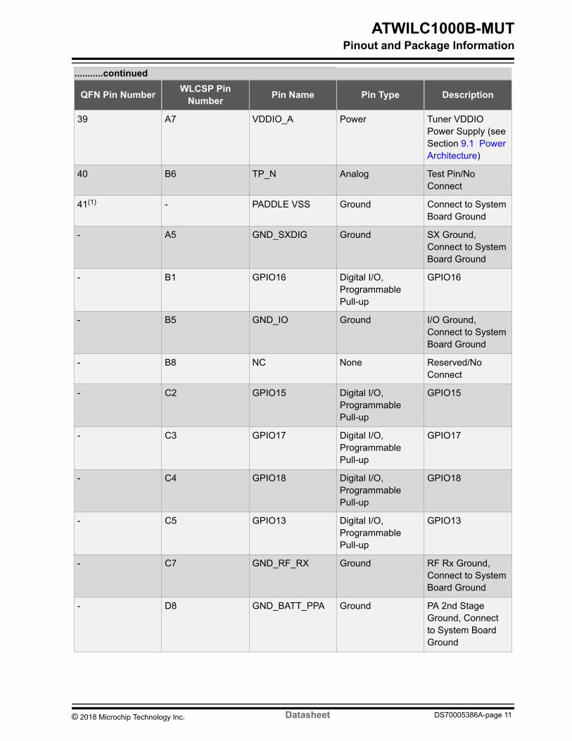
continued
QFN Pin Number WLCSP PinNumber Pin Name Pin Type Description
39 A7 VDDIO_A Power Tuner VDDIOPower Supply (seeSection 91 PowerArchitecture)
40 B6 TP_N Analog Test PinNoConnect
41(1) - PADDLE VSS Ground Connect to SystemBoard Ground
- A5 GND_SXDIG Ground SX GroundConnect to SystemBoard Ground
- B1 GPIO16 Digital IOProgrammablePull-up
GPIO16
- B5 GND_IO Ground IO GroundConnect to SystemBoard Ground
- B8 NC None ReservedNoConnect
- C2 GPIO15 Digital IOProgrammablePull-up
GPIO15
- C3 GPIO17 Digital IOProgrammablePull-up
GPIO17
- C4 GPIO18 Digital IOProgrammablePull-up
GPIO18
- C5 GPIO13 Digital IOProgrammablePull-up
GPIO13
- C7 GND_RF_RX Ground RF Rx GroundConnect to SystemBoard Ground
- D8 GND_BATT_PPA Ground PA 2nd StageGround Connectto System BoardGround
ATWILC1000B-MUTPinout and Package Information
copy 2018 Microchip Technology Inc Datasheet DS70005386A-page 11
continued
QFN Pin Number WLCSP PinNumber Pin Name Pin Type Description
- E1 VSS Ground Connect to SystemBoard Ground
- E7 GND_BATT_PA Ground PA 1st StageGround Connectto System BoardGround
- F1 GND_BIAS Ground Bias GroundConnect to SystemBoard Ground
- F7 GND_AMS Ground AMS GroundConnect to SystemBoard Ground
- F8 TX_P Analog Positive RFDifferential IO
- G1 GND_BUCK Ground DCDC ConverterGround Connectto System BoardGround
- G6 GPIO12 Digital IOProgrammablePull-up
GPIO12
- G8 TX_N Analog Negative RFDifferential IO
- H4 VSS Ground Connect to SystemBoard Ground
- H7 GPIO11 Digital IOProgrammablePull-up
GPIO11
Note 1 Applies to QFN package only Pin 41 PADDLE_VSS must be soldered to GND providing good RF
grounding and good heat dissipation
ATWILC1000B-MUTPinout and Package Information
copy 2018 Microchip Technology Inc Datasheet DS70005386A-page 12
Figure 3-3 WLCSP ATWILC1000B UU
32 Package DescriptionThe ATWILC1000B QFN package information is provided in the following table and the package view isshown in Figure 3-4
Table 3-2 QFN Package Information
Parameter Value Unit Tolerance
Package size 5 x 5 mm plusmn01 mm
QFN pad count 40 ndash ndash
Total thickness 085 mm +015-005mm
QFN pad pitch 040 ndash
Pad width 020 ndash
Exposed pad size 37 x 37 ndash
The ATWILC1000B WLCSP package information is provided in the following table and the package viewis shown in the Figure 3-5
Table 3-3 WLCSP Package Information
Parameter Value Unit Tolerance
Package size 324 x 324
mm
plusmn03 mm
Total thickness 056 plusmn03 mm
IO Pitch 035 ndash
Ball diameter 020 plusmn03 mm
ATWILC1000B-MUTPinout and Package Information
copy 2018 Microchip Technology Inc Datasheet DS70005386A-page 13
Figure 3-4 QFN Package
Figure 3-5 WLCSP Package
ATWILC1000B-MUTPinout and Package Information
copy 2018 Microchip Technology Inc Datasheet DS70005386A-page 14
4 Electrical Specifications
41 Absolute RatingsThe values listed in this section are the peaked excursions ratings that can be tolerated by the deviceand if sustained will cause irreparable damage to the device
Table 4-1 Absolute Maximum Ratings
Characteristics Symbol Min Max Unit
Core supply voltage VDDC -03 15
V
IO supply voltage VDDIO -03 50
Battery supply voltage VBATT -03 50
Digital input voltage VIN (1) -03 VDDIO
Analog input voltage VAIN (2) -03 15
ESD human body model VESDHBM (3) -1000 -2000 (3) +1000 +2000 (3)
Storage temperature TA -65 150ordmC
Junction temperature ndash ndash 125
RF input power max ndash ndash 23 dBm
Note 1 VIN corresponds to all the digital pins2 VAIN corresponds to the following analog pins VDD_RF_RX VDD_RF_TX VDD_AMS RFIOP
RFION XO_N XO_P VDD_SXDIG and VDD_VCO3 For VESDHBM each pin is classified as Class 1 or Class 2 or both
ndash The Class 1 pins include all the pins (both analog and digital)ndash The Class 2 pins are all digital pins onlyndash VESDHBM is plusmn1 kV for Class 1 pins VESDHBM is plusmn2 kV for Class 2 pins
42 Recommended Operating ConditionsThe recommended operating conditions for the ATWILC1000B are listed in the following table
Table 4-2 Recommended Operating Conditions
Characteristics Symbol Min Typ Max Unit
IO supply voltage VDDIO 27 33 36V
Battery supply voltage VBATT 300 330 420
Operating temperature ndash -40 ndash 85 ordmC
ATWILC1000B-MUTElectrical Specifications
copy 2018 Microchip Technology Inc Datasheet DS70005386A-page 15
Note 1 The ATWILC1000B is functional across this range of voltages however optimal RF performance is
ensured for VBATT in the range 30V lt VBATT lt 42V2 IO supply voltage is applied to the VDDIO_A and VDDIO pins3 Battery supply voltage is applied to the VDD_BATT_PPA VDD_BATT_PA and VBATT_BUCK pins4 See Table 9-4 for the details of power connections
43 DC Electrical CharacteristicsThe following table provides the DC characteristics for the ATWILC1000B digital pads
Table 4-3 DC Electrical Characteristics
Characteristic Min Typ Max Unit
Input Low Voltage(VIL)
-030 ndash 060
V
Input High Voltage(VIH)
VDDIO-060 ndash VDDIO+030
Output LowVoltage (VOL)
ndash ndash 045
Output HighVoltage (OVOH)
VDDIO-050 ndash ndash
Output Loading ndash ndash 20pF
Digital Input Load ndash ndash 6
Pad Drive Strength(regular pads (1))
106 135 ndash
mAPad Drive Strength(high-drive pads (1))
212 27 ndash
Note 1 The following are high-drive pads I2C_SCL I2C_SDA all other pads are regular
ATWILC1000B-MUTElectrical Specifications
copy 2018 Microchip Technology Inc Datasheet DS70005386A-page 16
5 Clocking
51 Crystal OscillatorThe following table provides the crystal oscillator parameters of the ATWILC1000B
Table 5-1 Crystal Oscillator Parameters
Parameter Min Typ Max Unit
Crystal resonant frequency ndash 26 ndash MHz
Crystal equivalent series resistance ndash 50 150 Ω
Stability ndash Initial offset(1) -100 ndash 100ppm
Stability - Temperature and aging -25 ndash 25
Note 1 To ensure plusmn25 ppm under operating conditions frequency offset calibration is required
The following block diagram in figure XO Connections - (a) shows how the internal Crystal Oscillator(XO) is connected to the external crystal The XO has 5 pF internal capacitance (denoted as c_onchip inthe following figure) on each terminal XO_P and XO_N To bypass the crystal oscillator with an externalreference an external signal capable of driving 5 pF can be applied to the XO_N terminal as shown infollowing figure XO Connections - (b) The XO has 5 pF internal capacitance on each terminal XO_Pand XO_N This internal capacitance must be accounted for when calculating the external loadingcapacitance c_onboard for the XTAL
Figure 5-1 XO Connections (a) The Crystal Oscillator is Used (b) The Crystal Oscillator isBypassed
XO_N XO_P XO_N XO_P
External Clock
ATWILC1000 ATWILC1000
(a) (b)
c_onboard c_onboard
c_onchip c_onchip
The following table specifies the electrical and performance requirements for the external clock
ATWILC1000B-MUTClocking
copy 2018 Microchip Technology Inc Datasheet DS70005386A-page 17
Table 5-2 Bypass Clock Specification
Parameter Min Typ Max Unit Comments
Oscillationfrequency ndash 26 ndash MHz
Must drive 5 pFload at desiredfrequency
Voltage swing 05 ndash 12 VPPMust be ACcoupled
Stability ndashTemperatureand aging
-25ndash
+25 ppmndash
Phase noise ndash ndash -130 dBcHz At 10 kHz offset
Jitter (RMS) ndash ndash
lt1
psec Based onintegratedphase noisespectrum from1 kHz to 1 MHz
52 Low-Power OscillatorThe ATWILC1000B has an internally-generated 32 kHz clock to provide timing information for varioussleep functions Alternatively the ATWILC1000B allows for an external 32kHz clock to be used for thispurpose which is provided through pin 24 (RTC_CLK) Software selects whether the internal clock orexternal clock is used
The internal low-power clock is ring oscillator-based and has accuracy within 10000 ppm When usingthe internal low-power clock the advance wake-up time in the Beacon Monitoring mode has to beincreased by about 1 of the sleep time to compensate for the oscillator inaccuracy For example for theDTIM interval value of 1 wake-up time has to be increased by 1 ms
For any application targeting very low-power consumption an external 32 kHz RTC clock must be used
ATWILC1000B-MUTClocking
copy 2018 Microchip Technology Inc Datasheet DS70005386A-page 18
6 CPU and Memory Subsystem
61 ProcessorThe ATWILC1000B has a Cortus APS3 32-bit processor This processor performs many of the MACfunctions including but not limited to association authentication power management security keymanagement and MSDU aggregationde-aggregation In addition the processor provides flexibility forvarious modes of operation such as STA and AP modes
62 Memory SubsystemThe APS3 core uses a 128 KB instructionboot ROM along with a 160 KB instruction RAM and a 64 KBdata RAM In addition the device uses a 128 KB shared RAM accessible by the processor and MACwhich allows the APS3 core to perform various data management tasks on the TX and RX data packets
63 Nonvolatile Memory (eFuse)The ATWILC1000B has 768 bits of nonvolatile eFuse memory that can be read by the CPU after devicereset This nonvolatile One-Time-Programmable (OTP) memory can be used to store customer-specificparameters such as MAC address various calibration information such as TX power crystal frequencyoffset other software-specific configuration parameters and so on The eFuse is partitioned into six 128-bit banks Each bank has the same bit map which is shown in the following figure The purpose of thefirst 80 bits in each bank is fixed and the remaining 48 bits are general-purpose software dependent bitsor reserved for future use Since each bank can be programmed independently this allows for severalupdates of the device parameters following the initial programming eg updating the MAC addressRefer to the ATWILC1000 Programming Guide for the eFuse programming instructions
ATWILC1000B-MUTCPU and Memory Subsystem
copy 2018 Microchip Technology Inc Datasheet DS70005386A-page 19
Figure 6-1 eFuse Bit Map
Bank 0
Bank 1
Bank 2
Bank 3
Bank 4
Bank 5
F MAC ADDR
Used
Inva
lid
Version
Reserved
MACAD
DR
Used
FO
Flags
G
21 1 3 1
Use
d
TX Gain
Correct-
tion
Used
Freq
Offse
t
1 7
488 8 16
1 15
128 Bits
ATWILC1000B-MUTCPU and Memory Subsystem
copy 2018 Microchip Technology Inc Datasheet DS70005386A-page 20
7 WLAN SubsystemThe WLAN subsystem is composed of the Media Access Controller (MAC) and the Physical Layer (PHY)The following two subsections describe the MAC and PHY in detail
71 MAC
711 FeaturesThe ATWILC1000B IEEE80211 MAC supports the following functions
bull IEEE 80211bgnbull IEEE 80211e WMM QoS EDCAPCF Multiple Access Categories Traffic Schedulingbull Advanced IEEE 80211n Features
ndash Transmission and reception of aggregated MPDUs (A-MPDU)ndash Transmission and reception of aggregated MSDUs (A-MSDU)ndash Immediate Block Acknowledgmentndash Reduced Interframe Spacing (RIFS)
bull Support for IEEE 80211i and WFA Security with Key Managementndash WEP 64128ndash WPA-TKIPndash 128-bit WPA2 CCMP (AES)
bull Support for WAPI Securitybull Advanced Power Management
ndash Standard 80211 Power Save modendash Wi-Fi Alliancereg WMM-PS (U-APSD)
bull RTS-CTS and CTS-Self Supportbull Supports Either STA or AP Mode in the Infrastructure Basic Service Set Modebull Supports Independent Basic Service Set (IBSS)
712 DescriptionThe ATWILC1000B MAC is designed to operate at low power while providing high data throughput TheIEEE 80211 MAC functions are implemented with a combination of dedicated datapath engineshardwired control logic and a low-power high-efficiency microprocessor The combination of dedicatedlogic with a programmable processor provides optimal power efficiency and real-time response whileproviding the flexibility to accommodate evolving standards and future feature enhancements
Dedicated datapath engines with heavy computational are used to implement datapath functions Forexample an FCS engine checks the CRC of the transmitting and receiving packets and a cipher engineperforms all the required encryption and decryption operations for the WEP WPA-TKIP WPA2 CCMP-AES and WAPI security requirements
Control functions which have real-time requirements are implemented using hardwired control logicmodules These logic modules offer real-time response while maintaining configurability via theprocessor Examples of hardwired control logic modules are the channel access control module(implements EDCAHCCA Beacon TX control interframe spacing and so on) protocol timer module(responsible for the Network Access Vector back-off timing timing synchronization function and slotmanagement) MPDU handling module aggregationdeaggregation module block ACK controller
ATWILC1000B-MUTWLAN Subsystem
copy 2018 Microchip Technology Inc Datasheet DS70005386A-page 21
(implements the protocol requirements for burst block communication) and TXRX control FSMs(coordinate data movement between PHY-MAC interface cipher engine and the DMA interface to theTXRX FIFOs)
The MAC functions that are implemented in software on the microprocessor have the followingcharacteristics
bull Functions with high memory requirements or complex data structures Examples are associationtable management and power save queuing
bull Functions with low computational load or without critical real-time requirements Examples areauthentication and association
bull Functions which need flexibility and upgradeability Examples are beacon frame processing and QoSscheduling
72 PHY
721 FeaturesThe ATWILC1000B IEEE 80211 PHY supports the following functions
bull Single Antenna 1x1 Stream in 20 MHz Channelsbull Supports IEEE 80211b DSSS-CCK Modulation 1 2 55 and 11 Mbpsbull Supports IEEE 80211g OFDM Modulation 6 9 1218 24 36 48 and 54 Mbpsbull Supports IEEE 80211n HT Modulations MCS0-7 20 MHz 800 and 400 ns guard interval 65 72
130 144 195 217 260 289 390 433 520 578 585 650 and 722 Mbpsbull IEEE 80211n Mixed Mode Operationbull Per Packet TX Power Controlbull Advanced Channel EstimationEqualization Automatic Gain Control CCA CarrierSymbol Recovery
and Frame Detection
722 DescriptionThe ATWILC1000B WLAN PHY is designed to achieve reliable and power-efficient physical layercommunication specified by IEEE 80211 bgn in Single Stream mode with 20 MHz bandwidth Advancedalgorithms are used to achieve maximum throughput in a real-world communication environment withimpairments and interference The PHY implements all the required functions such as FFT filtering FEC(Viterbi decoder) frequency and timing acquisition and tracking channel estimation and equalizationcarrier sensing and clear channel assessment as well as the automatic gain control
73 RadioThis section describes the properties and characteristics of the ATWILC1000B and Wi-Fi radio transmitand receive performance capabilities of the device The performance measurements are taken at the RFpin assuming 50Ω impedance the RF performance is assured for room temperature of 25degC with aderating of 2-3dB at boundary conditions
Measurements were taken under typical conditions VBATT at 33V VDDIO at 33V and temperature at+25ordmC
ATWILC1000B-MUTWLAN Subsystem
copy 2018 Microchip Technology Inc Datasheet DS70005386A-page 22
Table 7-1 Features and Properties
Feature Description
Part Number ATWILC1000B
WLAN Standard IEEE 80211bgn Wi-Fi compliant
Host Interface SPI SDIO
Dimension L x W x H 217 x 147 x 21 (typical) mm
Frequency range 2412 GHz ~ 2472 GHz (24 GHz ISM band)
Number of channels 11 for North America 13 for Europe
Modulation 80211b DQPSK DBPSK CCK
80211gn OFDM64-QAM16-QAM QPSK BPSK
Data rate 80211b 1 2 55 11 Mbps80211g 6 9 12 18 24 36 48 54 Mbps
Data rate
(20 MHz short GI400ns)
80211n 72 144 217 289 433 578 65722Mbps
Operating temperature(1) -40degC to 85degC
Storage temperature -40degC to 125degC
Humidity Operating humidity 10 to 95 non-condensing
Storage humidity 5 to 95 non-condensing
Note 1 RF performance is ensured at room temperature of 25degC with a 2-3db change at boundary
conditions
731 Receiver PerformanceThe following are typical conditions for radio receiver performance
VBATT at 33V VDDIO at 33V temperature at 25degC and WLAN Channel 6 (2437 MHz)
The table below provides the receiver performance characteristics for the ATWILC1000B
Table 7-2 Receiver Performance
Parameter Description Min Typ Max Unit
Frequency - 2412 - 2472 MHz
Sensitivity 80211b 1 Mbps DSSS - -94 -
dBm2 Mbps DSSS - -91 -
55 Mbps DSSS - -89 -
11 Mbps DSSS - -86 -
ATWILC1000B-MUTWLAN Subsystem
copy 2018 Microchip Technology Inc Datasheet DS70005386A-page 23
continuedParameter Description Min Typ Max Unit
Sensitivity 80211g 6 Mbps OFDM - -88 -
dBm
9 Mbps OFDM - -87 -
12 Mbps OFDM - -86 -
18 Mbps OFDM - -84 -
24 Mbps OFDM - -82 -
36 Mbps OFDM - -78 -
48 Mbps OFDM - -74 -
54 Mbps OFDM - -73 -
Sensitivity 80211n (BW at 20 MHz) MCS 0 - -87 -
dBm
MCS 1 - -85 -
MCS 2 - -83 -
MCS 3 - -80 -
MCS 4 - -76 -
MCS 5 - -73 -
MCS 6 - -71 -
MCS 7 - -69 -
Maximum Receive Signal Level 1-11 Mbps DSSS - 0 -
dBm6-54 Mbps OFDM - -5 -
MCS 0 ndash 7 - -5 -
Adjacent Channel Rejection 1 Mbps DSSS (30 MHz offset) - 50 -
dB
11 Mbps DSSS (25 MHz offset) - 43 -
6 Mbps OFDM (25 MHz offset) - 40 -
54 Mbps OFDM (25 MHz offset) - 25 -
MCS 0 ndash 20 MHz BW (25 MHz offset) - 40 -
MCS 7 ndash 20 MHz BW (25 MHz offset) - 20 -
ATWILC1000B-MUTWLAN Subsystem
copy 2018 Microchip Technology Inc Datasheet DS70005386A-page 24
continuedParameter Description Min Typ Max Unit
Cellular Blocker Immunity 776-794 MHz CDMA - -14 -
dBm
824-849 MHz GSM - -10 -
880-915 MHz GSM - -10 -
1710-1785 MHz GSM - -15 -
1850-1910 MHz GSM - -15 -
1850-1910 MHz WCDMA - -24 -
1920-1980 MHz WCDMA - -24 -
732 Transmitter PerformanceThe following are typical conditions for radio transmitter performance
VBAT=33V VDDIO=33V temperature at 25degC and WLAN Channel 6 (2437 MHz)
The following table provides the transmitter performance characteristics for the ATWILC1000B
Table 7-3 Transmitter Performance
Parameter Description Min Typ Max Unit
Frequency - 2412 2472 MHz
Output power(1)-(2)ON_Transmit
80211b 1Mbps - 176 -
dBm
80211b 11Mbps - 182 -
80211g 6Mbps - 187 -
80211g 54Mbps - 167 -
80211n MCS 0 - 173 -
80211n MCS 7 - 138 -
TX power accuracy - - plusmn15 (2) dB
Carrier suppression 80211b mode - -194 -
dBc80211g mode - -275 -
80211n mode - -211 -
ATWILC1000B-MUTWLAN Subsystem
copy 2018 Microchip Technology Inc Datasheet DS70005386A-page 25
continuedParameter Description Min Typ Max Unit
Out of band Transmit Power 76-108 - -125 -
dBmHz
776-794 - -125 -
869-960 - -125 -
925-960 - -125 -
1570-1580 - -125 -
1805-1880 - -125 -
1930-1990 - -125 -
2110-2170 - -125 -
Harmonic output power(4) 2nd - -28 -
dBmMHz3rd - -33 -
4th - -40 -
5th - -28 -
Note 1 Measured at 80211 specification compliant EVMSpectral mask2 Measured after RF matching network3 Operating temperature range is -40ordmC to +85ordmC RF performance is ensured at a room temperature
range of 25ordmC with 2-3dB change at boundary conditions4 Measured at 11 Mbps DG (Digital Gain) = -7 WLAN Channel 6 (2437 MHz)5 With respect to TX power different (higherlower) RF output power settings may be used for
specific antennas andor enclosures in which case re-certification may be required6 The availability of some specific channels andor operational frequency bands are country
dependent and should be programmed at the host product factory to match the intendeddestination Regulatory bodies prohibit exposing the settings to the end user This requirementneeds to be taken care of via host implementation
ATWILC1000B-MUTWLAN Subsystem
copy 2018 Microchip Technology Inc Datasheet DS70005386A-page 26
8 External InterfacesThe ATWILC1000B external interfaces include
bull I2C slave for controlbull SPI slave and SDIO slave for control and data transferbull SPI master for external Flashbull I2C master for external EEPROMbull UART Debug Interfacebull General Purpose InputOutput (GPIO) pins
81 I2C Slave InterfaceThe I2C Slave interface used primarily for control by the host processor is a two-wire serial interfaceconsisting of a serial data line (SDA Pin 33) and a serial clock (SCL pin 32) It responds to the seven bitaddress value 0x60 The ATWILC1000B I2C supports I2C bus Version 21 - 2000 and can operate inStandard mode (with data rates up to 100 Kbs) and Fast mode (with data rates up to 400 Kbs) The I2CSlave is a synchronous serial interface The SDA line is a bidirectional signal and changes only while theSCL line is low except for STOP START and RESTART conditions The output drivers are open-drain toperform wire-AND functions on the bus The maximum number of devices on the bus is limited by onlythe maximum capacitance specification of 400 pF Data is transmitted in byte packages For specificinformation refer to the Philips Specification entitled ldquoThe I2C -Bus Specification Version 21rdquo The I2CSlave timing is provided in the following figure
Figure 8-1 I2C Slave Timing Diagram
tHL
SDA
SCL tHDSTA
tWL
tWH
tSUDAT tPR tHDDAT
tPR tPR
tLH tHL
tLH
tSUSTOtBUF
tSUSTAfSCL
The I2C Slave timing parameters are provided in the following table
Table 8-1 I2C Slave Timing Parameters
Parameter Symbol Min Max Unit Remarks
SCL clock frequency fSCL 0 400 kHz ndash
SCL low pulse width tWL 13 ndashmicros
ndash
SCL high pulse width tWH 06 ndash ndash
ATWILC1000B-MUTExternal Interfaces
copy 2018 Microchip Technology Inc Datasheet DS70005386A-page 27
continuedParameter Symbol Min Max Unit Remarks
SCL SDA fall time tHL ndash 300ns
ndash
SCL SDA rise time tLH ndash 300 This is dictated by externalcomponents
START setup time tSUSTA 06 ndashmicros
ndash
START hold time tHDSTA 06 ndash ndash
SDA setup time tSUDAT 100 ndash
ns
ndash
SDA hold time tHDDAT 0
40
ndash Slave and master default masterprogramming option
STOP setup time tSUSTO 06 ndashmicros
ndash
Bus free time between STOP and START tBUF 13 ndash ndash
Glitch pulse reject tPR 0 50 ns ndash
82 I2C Master InterfaceThe ATWILC1000B provides an I2C bus master which is intended primarily for accessing an externalEEPROM memory through a software-defined protocol The I2C Master is a two-wire serial interfaceconsisting of a serial data line (SDA) and a serial clock line (SCL) SDA can be configured on one of thefollowing pins SD_CLK (pin 19) GPIO1 (pin 24) GPIO6 (pin 31) or I2C_SDA (pin 33) SCL can beconfigured on one of the following pins GPIO0 (pin 10) SD_DAT3 (pin 12) GPIO4 (pin 29) or I2C_SCL(pin 32) For more specific instructions refer to the ATWILC1000 Programming Guide
The I2C master interface supports three speeds
bull Standard mode (100 kbs)bull Fast mode (400 kbs)bull High-Speed mode (34 Mbs)
The timing diagram of the I2C master interface is the same as that of the I2C slave interface (see Figure8-1) The timing parameters of I2C master are shown in the following table
Table 8-2 I2C Master Timing Parameters
Parameter Symbol Standard Mode Fast Mode High-Speed Mode Unit
Min Max Min Max Min Max
SCL clock frequency fSCL 0 100 0 400 0 3400 kHz
SCL high pulse width tWH 4 ndash 06 ndash 006 ndashmicros
SCL low pulse width tWL 47 ndash 13 ndash 016 ndash
ATWILC1000B-MUTExternal Interfaces
copy 2018 Microchip Technology Inc Datasheet DS70005386A-page 28
continuedParameter Symbol Standard Mode Fast Mode High-Speed Mode Unit
Min Max Min Max Min Max
SCL fall time tHLSCL ndash 300 ndash 300 10 40
nsSDA fall time tHLSDA ndash 300 300 10 80
SCL rise time tLHSCL ndash 1000 ndash 300 10 40
SDA rise time tLHSDA ndash 1000 ndash 300 10 80
START setup time tSUSTA 47 ndash 06 ndash 016 ndashmicros
START hold time tHDSTA 4 ndash 06 ndash 016 ndash
SDA setup time tSUDAT 250 ndash 100 ndash 10 ndashns
SDA hold time tHDDAT 5 ndash 40 ndash 0 70
STOP setup time tSUSTO 4 ndash 06 ndash 016 ndash
microsBus free time between STOP andSTART
tBUF 47 ndash 13 ndash ndash ndash
Glitch pulse reject tPR ndash ndash 0 50 ndash ndash
83 SPI Slave InterfaceThe ATWILC1000B provides a Serial Peripheral Interface (SPI) that operates as an SPI slave The SPISlave interface can be used for control and for serial IO of 80211 data The SPI Slave pins are mappedas shown in the the following table The RXD pin is same as Master Output Slave Input (MOSI) and theTXD pin is same as Master Input Slave Output (MISO) The SPI Slave is a full-duplex slave-synchronousserial interface that is available immediately following reset when pin 9 (SDIO_SPI_CFG) is tied toVDDIO
Table 8-3 SPI Slave Interface Pin Mapping
Pin Number SPI Function
9 CFG Must be tied to VDDIO
16 SSN Active Low Slave Select
18 SCK Serial Clock
13 RXD Serial Data Receive (MOSI)
17 TXD Serial Data Transmit (MISO)
When the SPI is not selected ie when SSN is high the SPI interface does not interfere with datatransfers between the serial-master and other serial-slave devices When the serial slave is not selectedits transmitted data output is buffered resulting in a high impedance drive onto the serial master receiveline
The SPI Slave interface responds to a protocol that allows an external host to read or write any register inthe chip as well as initiate DMA transfers For more details of the SPI protocol and more specificinstructions refer to the ATWILC1000 Programming Guide
ATWILC1000B-MUTExternal Interfaces
copy 2018 Microchip Technology Inc Datasheet DS70005386A-page 29
The SPI Slave interface supports four standard modes as determined by the Clock Polarity (CPOL) andClock Phase (CPHA) settings These modes are illustrated in table SPI Slave Modes and Figure 8-2 Thered lines in this figure correspond to Clock Phase = 0 and the blue lines correspond to Clock Phase = 1
Table 8-4 SPI Slave Modes
Mode CPOL CPHA
0 0 0
1 0 1
2 1 0
3 1 1
Figure 8-2 SPI Slave Clock Polarity and Clock Phase Timing
z
z z
z
SCKCPOL = 0
CPOL = 1
SSN
RXDTXD(MOSIMISO)
CPHA = 0
CPHA = 1
2 3 4 5 6 7 8
1 2 3 4 5 6 7
1
8
The SPI slave timing is provided in the following figure
ATWILC1000B-MUTExternal Interfaces
copy 2018 Microchip Technology Inc Datasheet DS70005386A-page 30
Figure 8-3 SPI Slave Timing Diagram
The SPI slave timing parameters are provided in the following table
Table 8-5 SPI Slave Timing Parameters
Parameter Symbol Min Max Unit
Clock input frequency fSCK ndash 48 MHz
Clock low pulse width tWL 15 ndash
ns
Clock high pulse width tWH 15 ndash
Clock rise time tLH ndash 10
Clock fall time tHL ndash 10
Input setup time tISU 5 ndash
Input hold time tIHD 5 ndash
Output delay tODLY 0 20
Slave select setup time tSUSSN 5 ndash
Slave select hold time tHDSSN 5 ndash
84 SPI Master InterfaceThe ATWILC1000B provides an SPI master interface for accessing external Flash memory The SPImaster pins are mapped as shown in the following table The TXD pin is same as Master Output SlaveInput (MOSI) and the RXD pin is same as Master Input Slave Output (MISO) The SPI master interfacesupports all four standard modes of clock polarity and clock phase shown in Table 8-4 External SPI Flash
ATWILC1000B-MUTExternal Interfaces
copy 2018 Microchip Technology Inc Datasheet DS70005386A-page 31
memory is accessed by a processor programming commands to the SPI master interface which in turninitiates a SPI master access to the Flash For more specific instructions refer to the ATWILC1000Programming Guide
Table 8-6 SPI Master Interface Pin Mapping
Pin Number Pin Name SPI Function
28 GPIO3 SCK Serial Clock Output
29 GPIO4 SCK Active-Low Slave Select Output
30 GPIO5 TXD Serial Data Transmit Output (MOSI)
31 GPIO6 RXD Serial Data Receive Input (MISO)
The SPI master timing is provided in the following figure
Figure 8-4 SPI Master Timing Diagram
fSCK
tWHtLH
tHL
tWL
tODLY tISU tIHD
SCK
SSNTXD
RXD
The SPI master timing parameters are provided in the following table
Table 8-7 SPI Master Timing Parameters
Parameter Symbol Min Max Unit
Clock output frequency fSCK ndash 48 MHz
Clock low pulse width tWL 5 ndash
ns
Clock high pulse width tWH 5 ndash
Clock rise time tLH ndash 5
Clock fall time tHL ndash 5
Input setup time tISU 5 ndash
Input hold time tIHD 5 ndash
Output delay tODLY 0 5
ATWILC1000B-MUTExternal Interfaces
copy 2018 Microchip Technology Inc Datasheet DS70005386A-page 32
85 SDIO Slave InterfaceThe ATWILC1000B SDIO Slave is a full speed interface The interface supports the 1-bit4-bit SDTransfer mode at the clock range of 0 to 50 MHz The host can use this interface to read and write fromany register within the chip as well as configure the ATWILC1000B for data DMA To use this interfacepin 9 (SDIO_SPI_CFG) must be grounded The SDIO slave pins are mapped as shown in the followingtable
Table 8-8 SDIO Interface Pin Mapping
Pin Number SPI Function
9 CFG Must be tied to ground
12 DAT3 Data 3
13 DAT2 Data 2
16 DAT1 Data 1
17 DAT0 Data 0
18 CMD Command
19 CLK Clock
When the SDIO card is inserted into an SDIO aware host the detection of the card will be via the meansdescribed in SDIO specification During the normal initialization and interrogation of the card by the hostthe card identifies itself as an SDIO device The host software obtains the card information in a tuple(linked list) format and determines if that cardrsquos IO function(s) are acceptable to activate If the card isacceptable it is allowed to power-up fully and start the IO function(s) built into it The SD memory cardcommunication is based on an advanced 9-pin interface (clock command four data and three powerlines) designed to operate at a maximum operating frequency of 50 MHz The SDIO slave interface hasthe following features
bull Meets SDIO card specification version 20bull Host clock rate variable between 0 to 50 MHzbull 1 bit4-bit SD bus modes supportedbull Allows card to interrupt hostbull Responds to direct readwrite (IO52) and extended readwrite (IO53) transactionsbull Supports SuspendResume operation
The SDIO slave interface timing is provided in the following figure
ATWILC1000B-MUTExternal Interfaces
copy 2018 Microchip Technology Inc Datasheet DS70005386A-page 33
Figure 8-5 SDIO Slave Timing Diagram
The SDIO slave timing parameters are provided in the following table
Table 8-9 SDIO Slave Timing Parameters
Parameter Symbol Min Max Unit
Clock input frequency fPP 0 50 MHz
Clock low pulse width tWL 10 ndash
ns
Clock high pulse width tWH 10 ndash
Clock rise time tLH ndash 10
Clock fall time tHL ndash 10
Input setup time tISU 5 ndash
Input hold time tIH 5 ndash
Output delay tODLY 0 14
86 UART Debug InterfaceATWILC1000B has a Universal Asynchronous ReceiverTransmitter (UART) interface on pin 13 SD-DATA2SPI-RxD and pin 17 SD-DATA0SPI-TXD This interface should be used only for debuggingpurposes The UART is compatible with the RS-232 standard where ATWILC1000B-MUT operates asData Terminal Equipment (DTE) It has a two-pin RXDTXD interface
The default configuration for accessing the UART interface of ATWILC1000B-MUT is as followsbull Baud rate 115200bull Data 8 bitbull Parity None
ATWILC1000B-MUTExternal Interfaces
copy 2018 Microchip Technology Inc Datasheet DS70005386A-page 34
bull Stop bit 1 bitbull Flow control None
It also has Rx and Tx FIFOs which ensures reliable high speed reception and low software overheadtransmission FIFO size is 4x8 for both Rx and Tx direction The UART has status registers that show thenumber of received characters available in the FIFO and various error conditions in addition it has theability to generate interrupts based on these status bits
An example of UART receiving or transmitting a single packet is shown in the following figure Thisexample shows 7-bit data (0x45) odd parity and two stop bits
Figure 8-6 Example of UART RX or TX Packet
87 GPIOsNine General Purpose InputOutput (GPIO) pins labeled GPIO 0-8 are available to allow for applicationspecific functions Each GPIO pin can be programmed as an input (the value of the pin can be read bythe host or internal processor) or as an output (the output values can be programmed by the host orinternal processor) where the default mode after power-up is input GPIOs 7 and 8 are only availablewhen the host does not use the SDIO interface which shares two of its pins with these GPIOs Thereforefor SDIO-based applications seven GPIOs (0-6) are available For more specific usage instructions referto the ATWILC1000 Programming Guide
ATWILC1000B-MUTExternal Interfaces
copy 2018 Microchip Technology Inc Datasheet DS70005386A-page 35
9 Power Management
91 Power ArchitectureThe ATWILC1000B uses an innovative power architecture to eliminate the need for external regulatorsand reduce the number of off-chip components This architecture is shown in the following figure ThePower Management Unit (PMU) has a DCDC Converter that converts VBATT to the core supply used bythe digital and RFAMS blocks The PA and eFuse are supplied by dedicated LDOs and the VCO issupplied by a separate LDO structure The power connections in the following figure provide a conceptualframework for understanding the ATWILC1000B power architecture
Figure 9-1 Power Architecture
VBATT _BUCKOff-Chip
LC
RFAMS Core
Sleep Osc RF
AM
S C
ore
Volta
ge
VSW
VREG_BUCK
VDD_AMS VDD_RF VDD_SXDIG
LDO1VDDIO_A VDD_VCO
LDO2
~VDD_BATT
12V
10V
CHIP_EN
EFuse LDO
SX
Digital Core
DCDC Converter
EFuse
PA
PMU
RFAMS
DigitalVDDC
Dig CoreLDO
25V
PadsVDDIO
SleepLDO
Digital Core Voltage
dcdc_ena
enaena
Vin Vout
enaena
The following table provides the typical values for the digital and RFAMS core voltages
ATWILC1000B-MUTPower Management
copy 2018 Microchip Technology Inc Datasheet DS70005386A-page 36
Table 9-1 PMU Output Voltages
Parameter Typical
RFAMS core voltage (VREG_BUCK) 135V
Digital core voltage (VDDC) 110V
Refer to the reference design for an example of power supply connections including proper isolation ofthe supplies used by the digital and RFAMS blocks
92 Power ConsumptionThe ATWILC1000B has several device states
bull ON_Transmit ndash Device is actively transmitting an 80211 signalbull ON_Receive ndash Device is actively receiving an 80211 signalbull ON_Doze ndash Device is on but is neither transmitting nor receivingbull Power_Down ndash Device core supply off (leakage)
The following pins are used to switch between the ON and Power_Down statesbull CHIP_EN ndash Device pin (pin 23) used to enable DCDC Converterbull VDDIO ndash IO supply voltage from external supply
In the ON states VDDIO is on and CHIP_EN is high (at VDDIO voltage level) To switch between the ONstates and Power_Down state CHIP_EN has to change between high and low (GND) voltage WhenVDDIO is off and CHIP_EN is low the chip is powered off with no leakage (also see 93 Power-UpDownSequence)
921 Current Consumption in Various Device StatesThe following table provides the ATWILC1000B current consumption in various device states
Table 9-2 Current Consumption
Device State Code Rate Output Power(dBm)
Current Consumption(1)
IVBATT IVDDIO
ON_Transmit 80211b 1 Mbps 176 266 mA 22 mA
80211b 11 Mbps 185 239 mA 22 mA
80211g 6 Mbps 186 249 mA 22 mA
80211g 54 Mbps 169 173 mA 22 mA
80211n MCS 0 177 253 mA 22 mA
80211n MCS 7 140 164 mA 22 mA
ATWILC1000B-MUTPower Management
copy 2018 Microchip Technology Inc Datasheet DS70005386A-page 37
continuedDevice State Code Rate Output Power
(dBm)Current Consumption(1)
IVBATT IVDDIO
ON_Receive 80211b 1 Mbps NA 63 mA 22 mA
80211b 11 Mbps NA 63 mA 22 mA
80211g 6 Mbps NA 63 mA 22 mA
80211g 54 Mbps NA 63 mA 22 mA
80211n MCS 0 NA 63 mA 22 mA
80211n MCS 7 NA 63 mA 22 mA
ON_Doze NA NA 380 microA lt10 microA
Power_Down NA NA 125 μA (2)
Note 1 The power consumption values are measured when VBAT is 36V and VDDIO is 28V at 25degC
922 Controlling the Device StatesTable Device States shows how to switch between the device states using the following
bull CHIP_EN ndash Device pin (pin 23) used to enable DCDC Converterbull VDDIO ndash IO supply voltage from external supply
Table 9-3 Device States
Device State CHIP_EN VDDIO Power Consumption (1) (2)
IVBATT IVDDIO
ON_Transmit VDDIO On 172mA 18dBm (le18Mbps)
230mA 18dBm (gt18Mbps)
2mA
ON_Receive VDDIO On 60mA 2mA
ON_Doze VDDIO ON 280μA lt10μA
Power_Down GND On lt05μA lt02μA
Note 1 Conditions VBAT 36v IO18V2 Power consumption numbers are preliminary
923 Restrictions for Power StatesWhen no power is supplied to the device ie the DCDC converter output and VDDIO are both off (atground potential) In this case a voltage cannot be applied to the device pins because each pin containsan ESD diode from the pin to supply This diode turns on when voltage higher than one diode-drop issupplied to the pin
If a voltage must be applied to the signal pads while the chip is in a low power state the VDDIO supplymust be on so the SLEEP or Power_Down state must be used
ATWILC1000B-MUTPower Management
copy 2018 Microchip Technology Inc Datasheet DS70005386A-page 38
Similarly to prevent the pin-to-ground diode from turning on do not apply a voltage that is more than onediode-drop below ground to any pin
93 Power-UpDown SequenceThe power-updown sequence for the ATWILC1000B is shown in the following figure
Figure 9-2 Power-UpDown Sequence
VBATT
VDDIO
CHIP_EN
RESETN
tBIO
t IOCE
tCER
XO Clock
The timing parameters are provided in the following table
Table 9-4 Power-UpDown Sequence Timing
Parameter Min Max Unit Description Notes
tA 0 ndash
ms
VBATT rise to VDDIOrise
VBATT and VDDIO can rise simultaneously orcan be tied together VDDIO must not risebefore VBATT
tB 0 ndash VDDIO rise toCHIP_EN rise
CHIP_EN must not rise before VDDIOCHIP_EN must be driven high or low not leftfloating
tC 5 ndash CHIP_EN rise toRESETN rise
This delay is needed because XO clock muststabilize before RESETN removal RESETNmust be driven high or low not left floating
tA 0 ndash VDDIO fall to VBATTfall
VBATT and VDDIO can fall simultaneously orcan be tied together VBATT must not fall beforeVDDIO
tB 0 ndash CHIP_EN fall to VDDIOfall
VDDIO must not fall before CHIP_ENCHIP_EN and RESETN can fall simultaneously
tC 0 ndash RESETN fall to VDDIOfall
VDDIO must not fall before RESETN RESETNand CHIP_EN can fall simultaneously
ATWILC1000B-MUTPower Management
copy 2018 Microchip Technology Inc Datasheet DS70005386A-page 39
94 Digital IO Pin Behavior During Power-up SequencesThe following table represents digital IO pin states corresponding to device power modes
Table 9-5 Digital IO Pin Behavior in Different Device States
Device State VDDIO CHIP_EN RESETN Output Driver InputDriver
Pull-UpDownResistor (96kΩ)
Power_Down
core supply off
High Low Low Disabled (Hi-Z) Disabled Disabled
Power-On Reset
core supply on hardreset on
High High Low Disabled (Hi-Z) Disabled Enabled
Power-On Default
core supply on deviceout of reset but notprogrammed yet
High High High Disabled (Hi-Z) Enabled Enabled
On_DozeOn_TransmitOn_Receive
core supply on deviceprogrammed byfirmware
High High High Programmed byfirmware for eachpin
Enabled orDisabled
Oppositeof outputdriver state
Programmed byfirmware foreach pin
Enabled orDisabled
ATWILC1000B-MUTPower Management
copy 2018 Microchip Technology Inc Datasheet DS70005386A-page 40
10 Reference DesignThe ATWILC1000B reference design schematic is shown in the following figure
Figure 10-1 ATWILC1000B Reference Schematic
47u
F
22u
H
Not
e1
Add
Tes
t poi
nts
for I
2C_S
CL
and
I2C
_SD
A pi
ns2
Add
Tes
t poi
nts
for U
ART
TxD
and
RxD
pin
s
22u
H
ATWILC1000B-MUTReference Design
copy 2018 Microchip Technology Inc Datasheet DS70005386A-page 41
11 Reflow Profile InformationThis section provides the guidelines for the reflow process to get ATWILC1000B soldered to thecustomers design
111 Storage Condition
1111 Moisture Barrier Bag Before OpeningA moisture barrier bag must be stored in a temperature of less than 30degC with humidity under 85 RHThe calculated shelf life for the dry-packed product shall be 12 months from the date the bag is sealed
1112 Moisture Barrier Bag OpenHumidity indicator cards must be blue indicating that the humidity is lt30
112 Solder PasteSnAgCu eutectic solder with melting temperature of 217degC is most commonly used for lead-free solderreflow application This alloy is widely accepted in the semiconductor industry due to its low costrelatively low melting temperature and good thermal fatigue resistance Some recommended pastesinclude NC-SMQreg 230 flux and Indalloyreg 241 solder paste made up of 955 Sn38 Ag07 Cu or SENJUN705-GRN3360-K2-V Type 3 no clean paste
113 Stencil DesignThe recommended stencil is laser-cut stainless-steel type with thickness of 100 microm to 130 microm andapproximately a 11 ratio of stencil opening to pad dimension To improve paste release a positive taperwith bottom opening 25 microm larger than the top is utilized Local manufacturing experience may find othercombinations of stencil thickness and aperture size to get good results
114 Printing ProcessThe printing process requires no significant changes compared to SnPb solder Any guidelinesrecommended by the paste manufacturers to accommodate paste specific characteristics should befollowed Post-print inspection and paste volume measurement is very critical to ensure good print qualityand uniform paste
115 Baking ConditionsATWILC1000B is rated at MSL level 3 After the sealed bag is opened no baking is required within 168hours as long as the devices are held at le 30degC60 RH or stored at lt 10 RH
ATWILC1000B requires baking before mounting ifbull The sealed bag has been open for more than 168 hoursbull The humidity indicator card reads more than 10bull SIPs need to be baked for eight hours at 125degC
ATWILC1000B-MUTReflow Profile Information
copy 2018 Microchip Technology Inc Datasheet DS70005386A-page 42
116 Soldering and Reflow ConditionOptimization of the reflow process is the most critical factor considered for lead-free soldering Thedevelopment of an optimal profile must account the paste characteristics the size of the board thedensity of the components the mix of the larger and smaller components and the peak temperaturerequirements of the components An optimized reflow process is the key to ensuring a successful lead-free assembly and achieves high yield and long-term solder joint reliability
Temperature ProfilingTemperature profiling must be performed for all new board designs by attaching thermocouples at thesolder joints on the top surface of the larger components and at multiple locations of the boards This isto ensure that all components are heated to a temperature above the minimum reflow temperatures andthe smaller components do not exceed the maximum temperature limit The SnAgCu solder alloy melts at~217degC so the reflow temperature peak at joint level must be 15 to 20degC higher than meltingtemperature The targeted solder joint temperature for the SnAgCu solder must be ~235degC For larger orsophisticated boards with a large mix of components it is also important to ensure that the temperaturedifference across the board is less than 10 degrees to minimize board warpage The maximumtemperature at the component body must not exceed the MSL3 qualification specification
1161 Reflow OvenIt is strongly recommended that a reflow oven equipped with more heating zones and Nitrogenatmosphere be used for lead-free assembly Nitrogen atmosphere has shown to improve the wet-abilityand reduce temperature gradient across the board It can also enhance the appearance of the solderjoints by reducing the effects of oxidation
The following items should also be observed in the reflow process1 Some recommended pastes include
ndash NC-SMQreg 230 flux and Indalloyreg 241 solder paste made up of 955 Sn38 Ag07 Cundash SENJU N705-GRN3360-K2-V Type 3 no clean paste
2 Allowable reflow soldering iterationsndash Three times based on the following reflow soldering profile (refer following Figure)
3 Temperature profilendash Reflow soldering shall be done according to the following temperature profile (refer to the
following figure)ndash Peak temperature 250degC
ATWILC1000B-MUTReflow Profile Information
copy 2018 Microchip Technology Inc Datasheet DS70005386A-page 43
Figure 11-1 Solder Reflow Profile
Cleaning
The exposed ground paddle helps to self-align ATWILC1000B avoiding pad misalignment The use ofno-clean solder pastes is recommended Full drying of no-clean paste fluxes must be ensured as a resultof the reflow process This may require longer reflow profiles andor peak temperatures toward the highend of the process window as recommended by the solder paste vendor It is believed that uncured fluxresidues could lead to corrosion andor shorting in accelerated testing and possibly the field
Rework
Rework is to remove the mounted SIP package and replace with a new unit It is recommended that onceATWILC1000B has been removed it should never be reused During the rework process the mountedATWILC1000B and PCB are heated partially and ATWILC1000B is removed It is recommended to heat-proof the proximity of the mounted parts and junctions and use the best nozzle for rework that is suited tothe module size
ATWILC1000B-MUTReflow Profile Information
copy 2018 Microchip Technology Inc Datasheet DS70005386A-page 44
12 Reference Documentation and SupportThe following table provides the set of collateral documents to ease integration and device ramp
Table 12-1 Reference Documents
Title Content
Design FilesPackage
User Guide Schematic PCB layout Gerber BOM and System notes on RFRadio Full Test Report radiation pattern design guidelines temperatureperformance ESD
Platform Gettingstarted Guide
How-to-use package Out of the Box starting guide HW limitations and notes SWQuick start guidelines
HW Design Guide Best practices and recommendations to design a board with the product includingAntenna Design for Wi-Fi (layout recommendations types of antennas impedancematching using a power amplifier etc) SPIUART protocol between Wi-Fi SoCand the Host MCU
SW Design Guide Integration guide with clear description of High level Arch overview on how towrite a networking application list all API parameters and structures
Features of the device SPIhandshake protocol between device and host MCUflowsequence state diagram and timing
SW ProgrammerGuide
Explains in detail the flow chart and how to use each API to implement all genericuse cases (eg start AP start STA provisioning UDP TCP http TLS p2p errorsmanagement connectiontransfer recovery mechanismstate diagram) ndash usageand sample application note
For a complete listing of development-support tools and documentation visit the ATWILC1000 webpageor refer to the customer support section on options to contact the nearest Microchip field representative
ATWILC1000B-MUTReference Documentation and Support
copy 2018 Microchip Technology Inc Datasheet DS70005386A-page 45
13 Document Revision HistoryRevision Date Section Description
A 122018 Document bull Updated from Atmelto Microchiptemplate
bull Assigned a newMicrochip documentnumber Previousversion is Atmel42351 revision D
bull ISBN numberadded
Document Revision History-Atmel
Doc Rev Date Comments
42351D 052015 DS update to Rev B offering
Changes from ATWILC1000A to ATWILC1000B
1 Added second UART increased UART data rates2 Increased instruction RAM size from 128KB to 160KB3 Updated pin MUX table added new options for various interfaces4 Improved description of Coexistence interface5 Added VDD_VCO switch and connection in the power architecture6 Updated power consumption numbers7 Updated reference schematic8 Changed RTC_CLK pad definition from pull-down to pull-up
42351C 022015 DS update new Atmel format
42351B 112014 Major document update new sections added replaced text in most sections newand updated drawings
42351A 072014 Initial document release
ATWILC1000B-MUTDocument Revision History
copy 2018 Microchip Technology Inc Datasheet DS70005386A-page 46
The Microchip Web Site
Microchip provides online support via our web site at httpwwwmicrochipcom This web site is used asa means to make files and information easily available to customers Accessible by using your favoriteInternet browser the web site contains the following information
bull Product Support ndash Data sheets and errata application notes and sample programs designresources userrsquos guides and hardware support documents latest software releases and archivedsoftware
bull General Technical Support ndash Frequently Asked Questions (FAQ) technical support requests onlinediscussion groups Microchip consultant program member listing
bull Business of Microchip ndash Product selector and ordering guides latest Microchip press releaseslisting of seminars and events listings of Microchip sales offices distributors and factoryrepresentatives
Customer Change Notification Service
Microchiprsquos customer notification service helps keep customers current on Microchip productsSubscribers will receive e-mail notification whenever there are changes updates revisions or erratarelated to a specified product family or development tool of interest
To register access the Microchip web site at httpwwwmicrochipcom Under ldquoSupportrdquo click onldquoCustomer Change Notificationrdquo and follow the registration instructions
Customer Support
Users of Microchip products can receive assistance through several channels
bull Distributor or Representativebull Local Sales Officebull Field Application Engineer (FAE)bull Technical Support
Customers should contact their distributor representative or Field Application Engineer (FAE) for supportLocal sales offices are also available to help customers A listing of sales offices and locations is includedin the back of this document
Technical support is available through the web site at httpwwwmicrochipcomsupport
Microchip Devices Code Protection Feature
Note the following details of the code protection feature on Microchip devices
bull Microchip products meet the specification contained in their particular Microchip Data Sheetbull Microchip believes that its family of products is one of the most secure families of its kind on the
market today when used in the intended manner and under normal conditionsbull There are dishonest and possibly illegal methods used to breach the code protection feature All of
these methods to our knowledge require using the Microchip products in a manner outside theoperating specifications contained in Microchiprsquos Data Sheets Most likely the person doing so isengaged in theft of intellectual property
bull Microchip is willing to work with the customer who is concerned about the integrity of their code
ATWILC1000B-MUT
copy 2018 Microchip Technology Inc Datasheet DS70005386A-page 47
bull Neither Microchip nor any other semiconductor manufacturer can guarantee the security of theircode Code protection does not mean that we are guaranteeing the product as ldquounbreakablerdquo
Code protection is constantly evolving We at Microchip are committed to continuously improving thecode protection features of our products Attempts to break Microchiprsquos code protection feature may be aviolation of the Digital Millennium Copyright Act If such acts allow unauthorized access to your softwareor other copyrighted work you may have a right to sue for relief under that Act
Legal Notice
Information contained in this publication regarding device applications and the like is provided only foryour convenience and may be superseded by updates It is your responsibility to ensure that yourapplication meets with your specifications MICROCHIP MAKES NO REPRESENTATIONS ORWARRANTIES OF ANY KIND WHETHER EXPRESS OR IMPLIED WRITTEN OR ORAL STATUTORYOR OTHERWISE RELATED TO THE INFORMATION INCLUDING BUT NOT LIMITED TO ITSCONDITION QUALITY PERFORMANCE MERCHANTABILITY OR FITNESS FOR PURPOSEMicrochip disclaims all liability arising from this information and its use Use of Microchip devices in lifesupport andor safety applications is entirely at the buyerrsquos risk and the buyer agrees to defendindemnify and hold harmless Microchip from any and all damages claims suits or expenses resultingfrom such use No licenses are conveyed implicitly or otherwise under any Microchip intellectualproperty rights unless otherwise stated
Trademarks
The Microchip name and logo the Microchip logo AnyRate AVR AVR logo AVR Freaks BitCloudchipKIT chipKIT logo CryptoMemory CryptoRF dsPIC FlashFlex flexPWR Heldo JukeBlox KeeLoqKleer LANCheck LINK MD maXStylus maXTouch MediaLB megaAVR MOST MOST logo MPLABOptoLyzer PIC picoPower PICSTART PIC32 logo Prochip Designer QTouch SAM-BA SpyNIC SSTSST Logo SuperFlash tinyAVR UNIO and XMEGA are registered trademarks of Microchip TechnologyIncorporated in the USA and other countries
ClockWorks The Embedded Control Solutions Company EtherSynch Hyper Speed Control HyperLightLoad IntelliMOS mTouch Precision Edge and Quiet-Wire are registered trademarks of MicrochipTechnology Incorporated in the USA
Adjacent Key Suppression AKS Analog-for-the-Digital Age Any Capacitor AnyIn AnyOut BodyComCodeGuard CryptoAuthentication CryptoAutomotive CryptoCompanion CryptoController dsPICDEMdsPICDEMnet Dynamic Average Matching DAM ECAN EtherGREEN In-Circuit Serial ProgrammingICSP INICnet Inter-Chip Connectivity JitterBlocker KleerNet KleerNet logo memBrain Mindi MiWimotorBench MPASM MPF MPLAB Certified logo MPLIB MPLINK MultiTRAK NetDetach OmniscientCode Generation PICDEM PICDEMnet PICkit PICtail PowerSmart PureSilicon QMatrix REAL ICERipple Blocker SAM-ICE Serial Quad IO SMART-IS SQI SuperSwitcher SuperSwitcher II TotalEndurance TSHARC USBCheck VariSense ViewSpan WiperLock Wireless DNA and ZENA aretrademarks of Microchip Technology Incorporated in the USA and other countries
SQTP is a service mark of Microchip Technology Incorporated in the USA
Silicon Storage Technology is a registered trademark of Microchip Technology Inc in other countries
GestIC is a registered trademark of Microchip Technology Germany II GmbH amp Co KG a subsidiary ofMicrochip Technology Inc in other countries
All other trademarks mentioned herein are property of their respective companies
ATWILC1000B-MUT
copy 2018 Microchip Technology Inc Datasheet DS70005386A-page 48
copy 2018 Microchip Technology Incorporated Printed in the USA All Rights Reserved
ISBN 978-1-5224-3998-1
Quality Management System Certified by DNV
ISOTS 16949Microchip received ISOTS-169492009 certification for its worldwide headquarters design and waferfabrication facilities in Chandler and Tempe Arizona Gresham Oregon and design centers in Californiaand India The Companyrsquos quality system processes and procedures are for its PICreg MCUs and dsPICreg
DSCs KEELOQreg code hopping devices Serial EEPROMs microperipherals nonvolatile memory andanalog products In addition Microchiprsquos quality system for the design and manufacture of developmentsystems is ISO 90012000 certified
ATWILC1000B-MUT
copy 2018 Microchip Technology Inc Datasheet DS70005386A-page 49
AMERICAS ASIAPACIFIC ASIAPACIFIC EUROPECorporate Office2355 West Chandler BlvdChandler AZ 85224-6199Tel 480-792-7200Fax 480-792-7277Technical SupporthttpwwwmicrochipcomsupportWeb AddresswwwmicrochipcomAtlantaDuluth GATel 678-957-9614Fax 678-957-1455Austin TXTel 512-257-3370BostonWestborough MATel 774-760-0087Fax 774-760-0088ChicagoItasca ILTel 630-285-0071Fax 630-285-0075DallasAddison TXTel 972-818-7423Fax 972-818-2924DetroitNovi MITel 248-848-4000Houston TXTel 281-894-5983IndianapolisNoblesville INTel 317-773-8323Fax 317-773-5453Tel 317-536-2380Los AngelesMission Viejo CATel 949-462-9523Fax 949-462-9608Tel 951-273-7800Raleigh NCTel 919-844-7510New York NYTel 631-435-6000San Jose CATel 408-735-9110Tel 408-436-4270Canada - TorontoTel 905-695-1980Fax 905-695-2078
Australia - SydneyTel 61-2-9868-6733China - BeijingTel 86-10-8569-7000China - ChengduTel 86-28-8665-5511China - ChongqingTel 86-23-8980-9588China - DongguanTel 86-769-8702-9880China - GuangzhouTel 86-20-8755-8029China - HangzhouTel 86-571-8792-8115China - Hong Kong SARTel 852-2943-5100China - NanjingTel 86-25-8473-2460China - QingdaoTel 86-532-8502-7355China - ShanghaiTel 86-21-3326-8000China - ShenyangTel 86-24-2334-2829China - ShenzhenTel 86-755-8864-2200China - SuzhouTel 86-186-6233-1526China - WuhanTel 86-27-5980-5300China - XianTel 86-29-8833-7252China - XiamenTel 86-592-2388138China - ZhuhaiTel 86-756-3210040
India - BangaloreTel 91-80-3090-4444India - New DelhiTel 91-11-4160-8631India - PuneTel 91-20-4121-0141Japan - OsakaTel 81-6-6152-7160Japan - TokyoTel 81-3-6880- 3770Korea - DaeguTel 82-53-744-4301Korea - SeoulTel 82-2-554-7200Malaysia - Kuala LumpurTel 60-3-7651-7906Malaysia - PenangTel 60-4-227-8870Philippines - ManilaTel 63-2-634-9065SingaporeTel 65-6334-8870Taiwan - Hsin ChuTel 886-3-577-8366Taiwan - KaohsiungTel 886-7-213-7830Taiwan - TaipeiTel 886-2-2508-8600Thailand - BangkokTel 66-2-694-1351Vietnam - Ho Chi MinhTel 84-28-5448-2100
Austria - WelsTel 43-7242-2244-39Fax 43-7242-2244-393Denmark - CopenhagenTel 45-4450-2828Fax 45-4485-2829Finland - EspooTel 358-9-4520-820France - ParisTel 33-1-69-53-63-20Fax 33-1-69-30-90-79Germany - GarchingTel 49-8931-9700Germany - HaanTel 49-2129-3766400Germany - HeilbronnTel 49-7131-67-3636Germany - KarlsruheTel 49-721-625370Germany - MunichTel 49-89-627-144-0Fax 49-89-627-144-44Germany - RosenheimTel 49-8031-354-560Israel - RarsquoananaTel 972-9-744-7705Italy - MilanTel 39-0331-742611Fax 39-0331-466781Italy - PadovaTel 39-049-7625286Netherlands - DrunenTel 31-416-690399Fax 31-416-690340Norway - TrondheimTel 47-72884388Poland - WarsawTel 48-22-3325737Romania - BucharestTel 40-21-407-87-50Spain - MadridTel 34-91-708-08-90Fax 34-91-708-08-91Sweden - GothenbergTel 46-31-704-60-40Sweden - StockholmTel 46-8-5090-4654UK - WokinghamTel 44-118-921-5800Fax 44-118-921-5820
Worldwide Sales and Service
copy 2018 Microchip Technology Inc Datasheet DS70005386A-page 50
- Introduction
- Features
- Table of Contents
- 1 Ordering Information and IC Marking
- 2 Block Diagram
- 3 Pinout and Package Information
-
- 31 Pin Description
- 32 Package Description
-
- 4 Electrical Specifications
-
- 41 Absolute Ratings
- 42 Recommended Operating Conditions
- 43 DC Electrical Characteristics
-
- 5 Clocking
-
- 51 Crystal Oscillator
- 52 Low-Power Oscillator
-
- 6 CPU and Memory Subsystem
-
- 61 Processor
- 62 Memory Subsystem
- 63 Nonvolatile Memory (eFuse)
-
- 7 WLAN Subsystem
-
- 71 MAC
-
- 711 Features
- 712 Description
-
- 72 PHY
-
- 721 Features
- 722 Description
-
- 73 Radio
-
- 731 Receiver Performance
- 732 Transmitter Performance
-
- 8 External Interfaces
-
- 81 I2C Slave Interface
- 82 I2C Master Interface
- 83 SPI Slave Interface
- 84 SPI Master Interface
- 85 SDIO Slave Interface
- 86 UART Debug Interface
- 87 GPIOs
-
- 9 Power Management
-
- 91 Power Architecture
- 92 Power Consumption
-
- 921 Current Consumption in Various Device States
- 922 Controlling the Device States
- 923 Restrictions for Power States
-
- 93 Power-UpDown Sequence
- 94 Digital IO Pin Behavior During Power-up Sequences
-
- 10 Reference Design
- 11 Reflow Profile Information
-
- 111 Storage Condition
-
- 1111 Moisture Barrier Bag Before Opening
- 1112 Moisture Barrier Bag Open
-
- 112 Solder Paste
- 113 Stencil Design
- 114 Printing Process
- 115 Baking Conditions
- 116 Soldering and Reflow Condition
-
- 1161 Reflow Oven
-
- 12 Reference Documentation and Support
- 13 Document Revision History
- The Microchip Web Site
- Customer Change Notification Service
- Customer Support
- Microchip Devices Code Protection Feature
- Legal Notice
- Trademarks
- Quality Management System Certified by DNV
- Worldwide Sales and Service
-
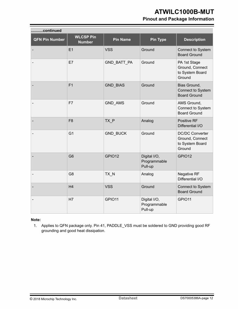
continued
QFN Pin Number WLCSP PinNumber Pin Name Pin Type Description
- E1 VSS Ground Connect to SystemBoard Ground
- E7 GND_BATT_PA Ground PA 1st StageGround Connectto System BoardGround
- F1 GND_BIAS Ground Bias GroundConnect to SystemBoard Ground
- F7 GND_AMS Ground AMS GroundConnect to SystemBoard Ground
- F8 TX_P Analog Positive RFDifferential IO
- G1 GND_BUCK Ground DCDC ConverterGround Connectto System BoardGround
- G6 GPIO12 Digital IOProgrammablePull-up
GPIO12
- G8 TX_N Analog Negative RFDifferential IO
- H4 VSS Ground Connect to SystemBoard Ground
- H7 GPIO11 Digital IOProgrammablePull-up
GPIO11
Note 1 Applies to QFN package only Pin 41 PADDLE_VSS must be soldered to GND providing good RF
grounding and good heat dissipation
ATWILC1000B-MUTPinout and Package Information
copy 2018 Microchip Technology Inc Datasheet DS70005386A-page 12
Figure 3-3 WLCSP ATWILC1000B UU
32 Package DescriptionThe ATWILC1000B QFN package information is provided in the following table and the package view isshown in Figure 3-4
Table 3-2 QFN Package Information
Parameter Value Unit Tolerance
Package size 5 x 5 mm plusmn01 mm
QFN pad count 40 ndash ndash
Total thickness 085 mm +015-005mm
QFN pad pitch 040 ndash
Pad width 020 ndash
Exposed pad size 37 x 37 ndash
The ATWILC1000B WLCSP package information is provided in the following table and the package viewis shown in the Figure 3-5
Table 3-3 WLCSP Package Information
Parameter Value Unit Tolerance
Package size 324 x 324
mm
plusmn03 mm
Total thickness 056 plusmn03 mm
IO Pitch 035 ndash
Ball diameter 020 plusmn03 mm
ATWILC1000B-MUTPinout and Package Information
copy 2018 Microchip Technology Inc Datasheet DS70005386A-page 13
Figure 3-4 QFN Package
Figure 3-5 WLCSP Package
ATWILC1000B-MUTPinout and Package Information
copy 2018 Microchip Technology Inc Datasheet DS70005386A-page 14
4 Electrical Specifications
41 Absolute RatingsThe values listed in this section are the peaked excursions ratings that can be tolerated by the deviceand if sustained will cause irreparable damage to the device
Table 4-1 Absolute Maximum Ratings
Characteristics Symbol Min Max Unit
Core supply voltage VDDC -03 15
V
IO supply voltage VDDIO -03 50
Battery supply voltage VBATT -03 50
Digital input voltage VIN (1) -03 VDDIO
Analog input voltage VAIN (2) -03 15
ESD human body model VESDHBM (3) -1000 -2000 (3) +1000 +2000 (3)
Storage temperature TA -65 150ordmC
Junction temperature ndash ndash 125
RF input power max ndash ndash 23 dBm
Note 1 VIN corresponds to all the digital pins2 VAIN corresponds to the following analog pins VDD_RF_RX VDD_RF_TX VDD_AMS RFIOP
RFION XO_N XO_P VDD_SXDIG and VDD_VCO3 For VESDHBM each pin is classified as Class 1 or Class 2 or both
ndash The Class 1 pins include all the pins (both analog and digital)ndash The Class 2 pins are all digital pins onlyndash VESDHBM is plusmn1 kV for Class 1 pins VESDHBM is plusmn2 kV for Class 2 pins
42 Recommended Operating ConditionsThe recommended operating conditions for the ATWILC1000B are listed in the following table
Table 4-2 Recommended Operating Conditions
Characteristics Symbol Min Typ Max Unit
IO supply voltage VDDIO 27 33 36V
Battery supply voltage VBATT 300 330 420
Operating temperature ndash -40 ndash 85 ordmC
ATWILC1000B-MUTElectrical Specifications
copy 2018 Microchip Technology Inc Datasheet DS70005386A-page 15
Note 1 The ATWILC1000B is functional across this range of voltages however optimal RF performance is
ensured for VBATT in the range 30V lt VBATT lt 42V2 IO supply voltage is applied to the VDDIO_A and VDDIO pins3 Battery supply voltage is applied to the VDD_BATT_PPA VDD_BATT_PA and VBATT_BUCK pins4 See Table 9-4 for the details of power connections
43 DC Electrical CharacteristicsThe following table provides the DC characteristics for the ATWILC1000B digital pads
Table 4-3 DC Electrical Characteristics
Characteristic Min Typ Max Unit
Input Low Voltage(VIL)
-030 ndash 060
V
Input High Voltage(VIH)
VDDIO-060 ndash VDDIO+030
Output LowVoltage (VOL)
ndash ndash 045
Output HighVoltage (OVOH)
VDDIO-050 ndash ndash
Output Loading ndash ndash 20pF
Digital Input Load ndash ndash 6
Pad Drive Strength(regular pads (1))
106 135 ndash
mAPad Drive Strength(high-drive pads (1))
212 27 ndash
Note 1 The following are high-drive pads I2C_SCL I2C_SDA all other pads are regular
ATWILC1000B-MUTElectrical Specifications
copy 2018 Microchip Technology Inc Datasheet DS70005386A-page 16
5 Clocking
51 Crystal OscillatorThe following table provides the crystal oscillator parameters of the ATWILC1000B
Table 5-1 Crystal Oscillator Parameters
Parameter Min Typ Max Unit
Crystal resonant frequency ndash 26 ndash MHz
Crystal equivalent series resistance ndash 50 150 Ω
Stability ndash Initial offset(1) -100 ndash 100ppm
Stability - Temperature and aging -25 ndash 25
Note 1 To ensure plusmn25 ppm under operating conditions frequency offset calibration is required
The following block diagram in figure XO Connections - (a) shows how the internal Crystal Oscillator(XO) is connected to the external crystal The XO has 5 pF internal capacitance (denoted as c_onchip inthe following figure) on each terminal XO_P and XO_N To bypass the crystal oscillator with an externalreference an external signal capable of driving 5 pF can be applied to the XO_N terminal as shown infollowing figure XO Connections - (b) The XO has 5 pF internal capacitance on each terminal XO_Pand XO_N This internal capacitance must be accounted for when calculating the external loadingcapacitance c_onboard for the XTAL
Figure 5-1 XO Connections (a) The Crystal Oscillator is Used (b) The Crystal Oscillator isBypassed
XO_N XO_P XO_N XO_P
External Clock
ATWILC1000 ATWILC1000
(a) (b)
c_onboard c_onboard
c_onchip c_onchip
The following table specifies the electrical and performance requirements for the external clock
ATWILC1000B-MUTClocking
copy 2018 Microchip Technology Inc Datasheet DS70005386A-page 17
Table 5-2 Bypass Clock Specification
Parameter Min Typ Max Unit Comments
Oscillationfrequency ndash 26 ndash MHz
Must drive 5 pFload at desiredfrequency
Voltage swing 05 ndash 12 VPPMust be ACcoupled
Stability ndashTemperatureand aging
-25ndash
+25 ppmndash
Phase noise ndash ndash -130 dBcHz At 10 kHz offset
Jitter (RMS) ndash ndash
lt1
psec Based onintegratedphase noisespectrum from1 kHz to 1 MHz
52 Low-Power OscillatorThe ATWILC1000B has an internally-generated 32 kHz clock to provide timing information for varioussleep functions Alternatively the ATWILC1000B allows for an external 32kHz clock to be used for thispurpose which is provided through pin 24 (RTC_CLK) Software selects whether the internal clock orexternal clock is used
The internal low-power clock is ring oscillator-based and has accuracy within 10000 ppm When usingthe internal low-power clock the advance wake-up time in the Beacon Monitoring mode has to beincreased by about 1 of the sleep time to compensate for the oscillator inaccuracy For example for theDTIM interval value of 1 wake-up time has to be increased by 1 ms
For any application targeting very low-power consumption an external 32 kHz RTC clock must be used
ATWILC1000B-MUTClocking
copy 2018 Microchip Technology Inc Datasheet DS70005386A-page 18
6 CPU and Memory Subsystem
61 ProcessorThe ATWILC1000B has a Cortus APS3 32-bit processor This processor performs many of the MACfunctions including but not limited to association authentication power management security keymanagement and MSDU aggregationde-aggregation In addition the processor provides flexibility forvarious modes of operation such as STA and AP modes
62 Memory SubsystemThe APS3 core uses a 128 KB instructionboot ROM along with a 160 KB instruction RAM and a 64 KBdata RAM In addition the device uses a 128 KB shared RAM accessible by the processor and MACwhich allows the APS3 core to perform various data management tasks on the TX and RX data packets
63 Nonvolatile Memory (eFuse)The ATWILC1000B has 768 bits of nonvolatile eFuse memory that can be read by the CPU after devicereset This nonvolatile One-Time-Programmable (OTP) memory can be used to store customer-specificparameters such as MAC address various calibration information such as TX power crystal frequencyoffset other software-specific configuration parameters and so on The eFuse is partitioned into six 128-bit banks Each bank has the same bit map which is shown in the following figure The purpose of thefirst 80 bits in each bank is fixed and the remaining 48 bits are general-purpose software dependent bitsor reserved for future use Since each bank can be programmed independently this allows for severalupdates of the device parameters following the initial programming eg updating the MAC addressRefer to the ATWILC1000 Programming Guide for the eFuse programming instructions
ATWILC1000B-MUTCPU and Memory Subsystem
copy 2018 Microchip Technology Inc Datasheet DS70005386A-page 19
Figure 6-1 eFuse Bit Map
Bank 0
Bank 1
Bank 2
Bank 3
Bank 4
Bank 5
F MAC ADDR
Used
Inva
lid
Version
Reserved
MACAD
DR
Used
FO
Flags
G
21 1 3 1
Use
d
TX Gain
Correct-
tion
Used
Freq
Offse
t
1 7
488 8 16
1 15
128 Bits
ATWILC1000B-MUTCPU and Memory Subsystem
copy 2018 Microchip Technology Inc Datasheet DS70005386A-page 20
7 WLAN SubsystemThe WLAN subsystem is composed of the Media Access Controller (MAC) and the Physical Layer (PHY)The following two subsections describe the MAC and PHY in detail
71 MAC
711 FeaturesThe ATWILC1000B IEEE80211 MAC supports the following functions
bull IEEE 80211bgnbull IEEE 80211e WMM QoS EDCAPCF Multiple Access Categories Traffic Schedulingbull Advanced IEEE 80211n Features
ndash Transmission and reception of aggregated MPDUs (A-MPDU)ndash Transmission and reception of aggregated MSDUs (A-MSDU)ndash Immediate Block Acknowledgmentndash Reduced Interframe Spacing (RIFS)
bull Support for IEEE 80211i and WFA Security with Key Managementndash WEP 64128ndash WPA-TKIPndash 128-bit WPA2 CCMP (AES)
bull Support for WAPI Securitybull Advanced Power Management
ndash Standard 80211 Power Save modendash Wi-Fi Alliancereg WMM-PS (U-APSD)
bull RTS-CTS and CTS-Self Supportbull Supports Either STA or AP Mode in the Infrastructure Basic Service Set Modebull Supports Independent Basic Service Set (IBSS)
712 DescriptionThe ATWILC1000B MAC is designed to operate at low power while providing high data throughput TheIEEE 80211 MAC functions are implemented with a combination of dedicated datapath engineshardwired control logic and a low-power high-efficiency microprocessor The combination of dedicatedlogic with a programmable processor provides optimal power efficiency and real-time response whileproviding the flexibility to accommodate evolving standards and future feature enhancements
Dedicated datapath engines with heavy computational are used to implement datapath functions Forexample an FCS engine checks the CRC of the transmitting and receiving packets and a cipher engineperforms all the required encryption and decryption operations for the WEP WPA-TKIP WPA2 CCMP-AES and WAPI security requirements
Control functions which have real-time requirements are implemented using hardwired control logicmodules These logic modules offer real-time response while maintaining configurability via theprocessor Examples of hardwired control logic modules are the channel access control module(implements EDCAHCCA Beacon TX control interframe spacing and so on) protocol timer module(responsible for the Network Access Vector back-off timing timing synchronization function and slotmanagement) MPDU handling module aggregationdeaggregation module block ACK controller
ATWILC1000B-MUTWLAN Subsystem
copy 2018 Microchip Technology Inc Datasheet DS70005386A-page 21
(implements the protocol requirements for burst block communication) and TXRX control FSMs(coordinate data movement between PHY-MAC interface cipher engine and the DMA interface to theTXRX FIFOs)
The MAC functions that are implemented in software on the microprocessor have the followingcharacteristics
bull Functions with high memory requirements or complex data structures Examples are associationtable management and power save queuing
bull Functions with low computational load or without critical real-time requirements Examples areauthentication and association
bull Functions which need flexibility and upgradeability Examples are beacon frame processing and QoSscheduling
72 PHY
721 FeaturesThe ATWILC1000B IEEE 80211 PHY supports the following functions
bull Single Antenna 1x1 Stream in 20 MHz Channelsbull Supports IEEE 80211b DSSS-CCK Modulation 1 2 55 and 11 Mbpsbull Supports IEEE 80211g OFDM Modulation 6 9 1218 24 36 48 and 54 Mbpsbull Supports IEEE 80211n HT Modulations MCS0-7 20 MHz 800 and 400 ns guard interval 65 72
130 144 195 217 260 289 390 433 520 578 585 650 and 722 Mbpsbull IEEE 80211n Mixed Mode Operationbull Per Packet TX Power Controlbull Advanced Channel EstimationEqualization Automatic Gain Control CCA CarrierSymbol Recovery
and Frame Detection
722 DescriptionThe ATWILC1000B WLAN PHY is designed to achieve reliable and power-efficient physical layercommunication specified by IEEE 80211 bgn in Single Stream mode with 20 MHz bandwidth Advancedalgorithms are used to achieve maximum throughput in a real-world communication environment withimpairments and interference The PHY implements all the required functions such as FFT filtering FEC(Viterbi decoder) frequency and timing acquisition and tracking channel estimation and equalizationcarrier sensing and clear channel assessment as well as the automatic gain control
73 RadioThis section describes the properties and characteristics of the ATWILC1000B and Wi-Fi radio transmitand receive performance capabilities of the device The performance measurements are taken at the RFpin assuming 50Ω impedance the RF performance is assured for room temperature of 25degC with aderating of 2-3dB at boundary conditions
Measurements were taken under typical conditions VBATT at 33V VDDIO at 33V and temperature at+25ordmC
ATWILC1000B-MUTWLAN Subsystem
copy 2018 Microchip Technology Inc Datasheet DS70005386A-page 22
Table 7-1 Features and Properties
Feature Description
Part Number ATWILC1000B
WLAN Standard IEEE 80211bgn Wi-Fi compliant
Host Interface SPI SDIO
Dimension L x W x H 217 x 147 x 21 (typical) mm
Frequency range 2412 GHz ~ 2472 GHz (24 GHz ISM band)
Number of channels 11 for North America 13 for Europe
Modulation 80211b DQPSK DBPSK CCK
80211gn OFDM64-QAM16-QAM QPSK BPSK
Data rate 80211b 1 2 55 11 Mbps80211g 6 9 12 18 24 36 48 54 Mbps
Data rate
(20 MHz short GI400ns)
80211n 72 144 217 289 433 578 65722Mbps
Operating temperature(1) -40degC to 85degC
Storage temperature -40degC to 125degC
Humidity Operating humidity 10 to 95 non-condensing
Storage humidity 5 to 95 non-condensing
Note 1 RF performance is ensured at room temperature of 25degC with a 2-3db change at boundary
conditions
731 Receiver PerformanceThe following are typical conditions for radio receiver performance
VBATT at 33V VDDIO at 33V temperature at 25degC and WLAN Channel 6 (2437 MHz)
The table below provides the receiver performance characteristics for the ATWILC1000B
Table 7-2 Receiver Performance
Parameter Description Min Typ Max Unit
Frequency - 2412 - 2472 MHz
Sensitivity 80211b 1 Mbps DSSS - -94 -
dBm2 Mbps DSSS - -91 -
55 Mbps DSSS - -89 -
11 Mbps DSSS - -86 -
ATWILC1000B-MUTWLAN Subsystem
copy 2018 Microchip Technology Inc Datasheet DS70005386A-page 23
continuedParameter Description Min Typ Max Unit
Sensitivity 80211g 6 Mbps OFDM - -88 -
dBm
9 Mbps OFDM - -87 -
12 Mbps OFDM - -86 -
18 Mbps OFDM - -84 -
24 Mbps OFDM - -82 -
36 Mbps OFDM - -78 -
48 Mbps OFDM - -74 -
54 Mbps OFDM - -73 -
Sensitivity 80211n (BW at 20 MHz) MCS 0 - -87 -
dBm
MCS 1 - -85 -
MCS 2 - -83 -
MCS 3 - -80 -
MCS 4 - -76 -
MCS 5 - -73 -
MCS 6 - -71 -
MCS 7 - -69 -
Maximum Receive Signal Level 1-11 Mbps DSSS - 0 -
dBm6-54 Mbps OFDM - -5 -
MCS 0 ndash 7 - -5 -
Adjacent Channel Rejection 1 Mbps DSSS (30 MHz offset) - 50 -
dB
11 Mbps DSSS (25 MHz offset) - 43 -
6 Mbps OFDM (25 MHz offset) - 40 -
54 Mbps OFDM (25 MHz offset) - 25 -
MCS 0 ndash 20 MHz BW (25 MHz offset) - 40 -
MCS 7 ndash 20 MHz BW (25 MHz offset) - 20 -
ATWILC1000B-MUTWLAN Subsystem
copy 2018 Microchip Technology Inc Datasheet DS70005386A-page 24
continuedParameter Description Min Typ Max Unit
Cellular Blocker Immunity 776-794 MHz CDMA - -14 -
dBm
824-849 MHz GSM - -10 -
880-915 MHz GSM - -10 -
1710-1785 MHz GSM - -15 -
1850-1910 MHz GSM - -15 -
1850-1910 MHz WCDMA - -24 -
1920-1980 MHz WCDMA - -24 -
732 Transmitter PerformanceThe following are typical conditions for radio transmitter performance
VBAT=33V VDDIO=33V temperature at 25degC and WLAN Channel 6 (2437 MHz)
The following table provides the transmitter performance characteristics for the ATWILC1000B
Table 7-3 Transmitter Performance
Parameter Description Min Typ Max Unit
Frequency - 2412 2472 MHz
Output power(1)-(2)ON_Transmit
80211b 1Mbps - 176 -
dBm
80211b 11Mbps - 182 -
80211g 6Mbps - 187 -
80211g 54Mbps - 167 -
80211n MCS 0 - 173 -
80211n MCS 7 - 138 -
TX power accuracy - - plusmn15 (2) dB
Carrier suppression 80211b mode - -194 -
dBc80211g mode - -275 -
80211n mode - -211 -
ATWILC1000B-MUTWLAN Subsystem
copy 2018 Microchip Technology Inc Datasheet DS70005386A-page 25
continuedParameter Description Min Typ Max Unit
Out of band Transmit Power 76-108 - -125 -
dBmHz
776-794 - -125 -
869-960 - -125 -
925-960 - -125 -
1570-1580 - -125 -
1805-1880 - -125 -
1930-1990 - -125 -
2110-2170 - -125 -
Harmonic output power(4) 2nd - -28 -
dBmMHz3rd - -33 -
4th - -40 -
5th - -28 -
Note 1 Measured at 80211 specification compliant EVMSpectral mask2 Measured after RF matching network3 Operating temperature range is -40ordmC to +85ordmC RF performance is ensured at a room temperature
range of 25ordmC with 2-3dB change at boundary conditions4 Measured at 11 Mbps DG (Digital Gain) = -7 WLAN Channel 6 (2437 MHz)5 With respect to TX power different (higherlower) RF output power settings may be used for
specific antennas andor enclosures in which case re-certification may be required6 The availability of some specific channels andor operational frequency bands are country
dependent and should be programmed at the host product factory to match the intendeddestination Regulatory bodies prohibit exposing the settings to the end user This requirementneeds to be taken care of via host implementation
ATWILC1000B-MUTWLAN Subsystem
copy 2018 Microchip Technology Inc Datasheet DS70005386A-page 26
8 External InterfacesThe ATWILC1000B external interfaces include
bull I2C slave for controlbull SPI slave and SDIO slave for control and data transferbull SPI master for external Flashbull I2C master for external EEPROMbull UART Debug Interfacebull General Purpose InputOutput (GPIO) pins
81 I2C Slave InterfaceThe I2C Slave interface used primarily for control by the host processor is a two-wire serial interfaceconsisting of a serial data line (SDA Pin 33) and a serial clock (SCL pin 32) It responds to the seven bitaddress value 0x60 The ATWILC1000B I2C supports I2C bus Version 21 - 2000 and can operate inStandard mode (with data rates up to 100 Kbs) and Fast mode (with data rates up to 400 Kbs) The I2CSlave is a synchronous serial interface The SDA line is a bidirectional signal and changes only while theSCL line is low except for STOP START and RESTART conditions The output drivers are open-drain toperform wire-AND functions on the bus The maximum number of devices on the bus is limited by onlythe maximum capacitance specification of 400 pF Data is transmitted in byte packages For specificinformation refer to the Philips Specification entitled ldquoThe I2C -Bus Specification Version 21rdquo The I2CSlave timing is provided in the following figure
Figure 8-1 I2C Slave Timing Diagram
tHL
SDA
SCL tHDSTA
tWL
tWH
tSUDAT tPR tHDDAT
tPR tPR
tLH tHL
tLH
tSUSTOtBUF
tSUSTAfSCL
The I2C Slave timing parameters are provided in the following table
Table 8-1 I2C Slave Timing Parameters
Parameter Symbol Min Max Unit Remarks
SCL clock frequency fSCL 0 400 kHz ndash
SCL low pulse width tWL 13 ndashmicros
ndash
SCL high pulse width tWH 06 ndash ndash
ATWILC1000B-MUTExternal Interfaces
copy 2018 Microchip Technology Inc Datasheet DS70005386A-page 27
continuedParameter Symbol Min Max Unit Remarks
SCL SDA fall time tHL ndash 300ns
ndash
SCL SDA rise time tLH ndash 300 This is dictated by externalcomponents
START setup time tSUSTA 06 ndashmicros
ndash
START hold time tHDSTA 06 ndash ndash
SDA setup time tSUDAT 100 ndash
ns
ndash
SDA hold time tHDDAT 0
40
ndash Slave and master default masterprogramming option
STOP setup time tSUSTO 06 ndashmicros
ndash
Bus free time between STOP and START tBUF 13 ndash ndash
Glitch pulse reject tPR 0 50 ns ndash
82 I2C Master InterfaceThe ATWILC1000B provides an I2C bus master which is intended primarily for accessing an externalEEPROM memory through a software-defined protocol The I2C Master is a two-wire serial interfaceconsisting of a serial data line (SDA) and a serial clock line (SCL) SDA can be configured on one of thefollowing pins SD_CLK (pin 19) GPIO1 (pin 24) GPIO6 (pin 31) or I2C_SDA (pin 33) SCL can beconfigured on one of the following pins GPIO0 (pin 10) SD_DAT3 (pin 12) GPIO4 (pin 29) or I2C_SCL(pin 32) For more specific instructions refer to the ATWILC1000 Programming Guide
The I2C master interface supports three speeds
bull Standard mode (100 kbs)bull Fast mode (400 kbs)bull High-Speed mode (34 Mbs)
The timing diagram of the I2C master interface is the same as that of the I2C slave interface (see Figure8-1) The timing parameters of I2C master are shown in the following table
Table 8-2 I2C Master Timing Parameters
Parameter Symbol Standard Mode Fast Mode High-Speed Mode Unit
Min Max Min Max Min Max
SCL clock frequency fSCL 0 100 0 400 0 3400 kHz
SCL high pulse width tWH 4 ndash 06 ndash 006 ndashmicros
SCL low pulse width tWL 47 ndash 13 ndash 016 ndash
ATWILC1000B-MUTExternal Interfaces
copy 2018 Microchip Technology Inc Datasheet DS70005386A-page 28
continuedParameter Symbol Standard Mode Fast Mode High-Speed Mode Unit
Min Max Min Max Min Max
SCL fall time tHLSCL ndash 300 ndash 300 10 40
nsSDA fall time tHLSDA ndash 300 300 10 80
SCL rise time tLHSCL ndash 1000 ndash 300 10 40
SDA rise time tLHSDA ndash 1000 ndash 300 10 80
START setup time tSUSTA 47 ndash 06 ndash 016 ndashmicros
START hold time tHDSTA 4 ndash 06 ndash 016 ndash
SDA setup time tSUDAT 250 ndash 100 ndash 10 ndashns
SDA hold time tHDDAT 5 ndash 40 ndash 0 70
STOP setup time tSUSTO 4 ndash 06 ndash 016 ndash
microsBus free time between STOP andSTART
tBUF 47 ndash 13 ndash ndash ndash
Glitch pulse reject tPR ndash ndash 0 50 ndash ndash
83 SPI Slave InterfaceThe ATWILC1000B provides a Serial Peripheral Interface (SPI) that operates as an SPI slave The SPISlave interface can be used for control and for serial IO of 80211 data The SPI Slave pins are mappedas shown in the the following table The RXD pin is same as Master Output Slave Input (MOSI) and theTXD pin is same as Master Input Slave Output (MISO) The SPI Slave is a full-duplex slave-synchronousserial interface that is available immediately following reset when pin 9 (SDIO_SPI_CFG) is tied toVDDIO
Table 8-3 SPI Slave Interface Pin Mapping
Pin Number SPI Function
9 CFG Must be tied to VDDIO
16 SSN Active Low Slave Select
18 SCK Serial Clock
13 RXD Serial Data Receive (MOSI)
17 TXD Serial Data Transmit (MISO)
When the SPI is not selected ie when SSN is high the SPI interface does not interfere with datatransfers between the serial-master and other serial-slave devices When the serial slave is not selectedits transmitted data output is buffered resulting in a high impedance drive onto the serial master receiveline
The SPI Slave interface responds to a protocol that allows an external host to read or write any register inthe chip as well as initiate DMA transfers For more details of the SPI protocol and more specificinstructions refer to the ATWILC1000 Programming Guide
ATWILC1000B-MUTExternal Interfaces
copy 2018 Microchip Technology Inc Datasheet DS70005386A-page 29
The SPI Slave interface supports four standard modes as determined by the Clock Polarity (CPOL) andClock Phase (CPHA) settings These modes are illustrated in table SPI Slave Modes and Figure 8-2 Thered lines in this figure correspond to Clock Phase = 0 and the blue lines correspond to Clock Phase = 1
Table 8-4 SPI Slave Modes
Mode CPOL CPHA
0 0 0
1 0 1
2 1 0
3 1 1
Figure 8-2 SPI Slave Clock Polarity and Clock Phase Timing
z
z z
z
SCKCPOL = 0
CPOL = 1
SSN
RXDTXD(MOSIMISO)
CPHA = 0
CPHA = 1
2 3 4 5 6 7 8
1 2 3 4 5 6 7
1
8
The SPI slave timing is provided in the following figure
ATWILC1000B-MUTExternal Interfaces
copy 2018 Microchip Technology Inc Datasheet DS70005386A-page 30
Figure 8-3 SPI Slave Timing Diagram
The SPI slave timing parameters are provided in the following table
Table 8-5 SPI Slave Timing Parameters
Parameter Symbol Min Max Unit
Clock input frequency fSCK ndash 48 MHz
Clock low pulse width tWL 15 ndash
ns
Clock high pulse width tWH 15 ndash
Clock rise time tLH ndash 10
Clock fall time tHL ndash 10
Input setup time tISU 5 ndash
Input hold time tIHD 5 ndash
Output delay tODLY 0 20
Slave select setup time tSUSSN 5 ndash
Slave select hold time tHDSSN 5 ndash
84 SPI Master InterfaceThe ATWILC1000B provides an SPI master interface for accessing external Flash memory The SPImaster pins are mapped as shown in the following table The TXD pin is same as Master Output SlaveInput (MOSI) and the RXD pin is same as Master Input Slave Output (MISO) The SPI master interfacesupports all four standard modes of clock polarity and clock phase shown in Table 8-4 External SPI Flash
ATWILC1000B-MUTExternal Interfaces
copy 2018 Microchip Technology Inc Datasheet DS70005386A-page 31
memory is accessed by a processor programming commands to the SPI master interface which in turninitiates a SPI master access to the Flash For more specific instructions refer to the ATWILC1000Programming Guide
Table 8-6 SPI Master Interface Pin Mapping
Pin Number Pin Name SPI Function
28 GPIO3 SCK Serial Clock Output
29 GPIO4 SCK Active-Low Slave Select Output
30 GPIO5 TXD Serial Data Transmit Output (MOSI)
31 GPIO6 RXD Serial Data Receive Input (MISO)
The SPI master timing is provided in the following figure
Figure 8-4 SPI Master Timing Diagram
fSCK
tWHtLH
tHL
tWL
tODLY tISU tIHD
SCK
SSNTXD
RXD
The SPI master timing parameters are provided in the following table
Table 8-7 SPI Master Timing Parameters
Parameter Symbol Min Max Unit
Clock output frequency fSCK ndash 48 MHz
Clock low pulse width tWL 5 ndash
ns
Clock high pulse width tWH 5 ndash
Clock rise time tLH ndash 5
Clock fall time tHL ndash 5
Input setup time tISU 5 ndash
Input hold time tIHD 5 ndash
Output delay tODLY 0 5
ATWILC1000B-MUTExternal Interfaces
copy 2018 Microchip Technology Inc Datasheet DS70005386A-page 32
85 SDIO Slave InterfaceThe ATWILC1000B SDIO Slave is a full speed interface The interface supports the 1-bit4-bit SDTransfer mode at the clock range of 0 to 50 MHz The host can use this interface to read and write fromany register within the chip as well as configure the ATWILC1000B for data DMA To use this interfacepin 9 (SDIO_SPI_CFG) must be grounded The SDIO slave pins are mapped as shown in the followingtable
Table 8-8 SDIO Interface Pin Mapping
Pin Number SPI Function
9 CFG Must be tied to ground
12 DAT3 Data 3
13 DAT2 Data 2
16 DAT1 Data 1
17 DAT0 Data 0
18 CMD Command
19 CLK Clock
When the SDIO card is inserted into an SDIO aware host the detection of the card will be via the meansdescribed in SDIO specification During the normal initialization and interrogation of the card by the hostthe card identifies itself as an SDIO device The host software obtains the card information in a tuple(linked list) format and determines if that cardrsquos IO function(s) are acceptable to activate If the card isacceptable it is allowed to power-up fully and start the IO function(s) built into it The SD memory cardcommunication is based on an advanced 9-pin interface (clock command four data and three powerlines) designed to operate at a maximum operating frequency of 50 MHz The SDIO slave interface hasthe following features
bull Meets SDIO card specification version 20bull Host clock rate variable between 0 to 50 MHzbull 1 bit4-bit SD bus modes supportedbull Allows card to interrupt hostbull Responds to direct readwrite (IO52) and extended readwrite (IO53) transactionsbull Supports SuspendResume operation
The SDIO slave interface timing is provided in the following figure
ATWILC1000B-MUTExternal Interfaces
copy 2018 Microchip Technology Inc Datasheet DS70005386A-page 33
Figure 8-5 SDIO Slave Timing Diagram
The SDIO slave timing parameters are provided in the following table
Table 8-9 SDIO Slave Timing Parameters
Parameter Symbol Min Max Unit
Clock input frequency fPP 0 50 MHz
Clock low pulse width tWL 10 ndash
ns
Clock high pulse width tWH 10 ndash
Clock rise time tLH ndash 10
Clock fall time tHL ndash 10
Input setup time tISU 5 ndash
Input hold time tIH 5 ndash
Output delay tODLY 0 14
86 UART Debug InterfaceATWILC1000B has a Universal Asynchronous ReceiverTransmitter (UART) interface on pin 13 SD-DATA2SPI-RxD and pin 17 SD-DATA0SPI-TXD This interface should be used only for debuggingpurposes The UART is compatible with the RS-232 standard where ATWILC1000B-MUT operates asData Terminal Equipment (DTE) It has a two-pin RXDTXD interface
The default configuration for accessing the UART interface of ATWILC1000B-MUT is as followsbull Baud rate 115200bull Data 8 bitbull Parity None
ATWILC1000B-MUTExternal Interfaces
copy 2018 Microchip Technology Inc Datasheet DS70005386A-page 34
bull Stop bit 1 bitbull Flow control None
It also has Rx and Tx FIFOs which ensures reliable high speed reception and low software overheadtransmission FIFO size is 4x8 for both Rx and Tx direction The UART has status registers that show thenumber of received characters available in the FIFO and various error conditions in addition it has theability to generate interrupts based on these status bits
An example of UART receiving or transmitting a single packet is shown in the following figure Thisexample shows 7-bit data (0x45) odd parity and two stop bits
Figure 8-6 Example of UART RX or TX Packet
87 GPIOsNine General Purpose InputOutput (GPIO) pins labeled GPIO 0-8 are available to allow for applicationspecific functions Each GPIO pin can be programmed as an input (the value of the pin can be read bythe host or internal processor) or as an output (the output values can be programmed by the host orinternal processor) where the default mode after power-up is input GPIOs 7 and 8 are only availablewhen the host does not use the SDIO interface which shares two of its pins with these GPIOs Thereforefor SDIO-based applications seven GPIOs (0-6) are available For more specific usage instructions referto the ATWILC1000 Programming Guide
ATWILC1000B-MUTExternal Interfaces
copy 2018 Microchip Technology Inc Datasheet DS70005386A-page 35
9 Power Management
91 Power ArchitectureThe ATWILC1000B uses an innovative power architecture to eliminate the need for external regulatorsand reduce the number of off-chip components This architecture is shown in the following figure ThePower Management Unit (PMU) has a DCDC Converter that converts VBATT to the core supply used bythe digital and RFAMS blocks The PA and eFuse are supplied by dedicated LDOs and the VCO issupplied by a separate LDO structure The power connections in the following figure provide a conceptualframework for understanding the ATWILC1000B power architecture
Figure 9-1 Power Architecture
VBATT _BUCKOff-Chip
LC
RFAMS Core
Sleep Osc RF
AM
S C
ore
Volta
ge
VSW
VREG_BUCK
VDD_AMS VDD_RF VDD_SXDIG
LDO1VDDIO_A VDD_VCO
LDO2
~VDD_BATT
12V
10V
CHIP_EN
EFuse LDO
SX
Digital Core
DCDC Converter
EFuse
PA
PMU
RFAMS
DigitalVDDC
Dig CoreLDO
25V
PadsVDDIO
SleepLDO
Digital Core Voltage
dcdc_ena
enaena
Vin Vout
enaena
The following table provides the typical values for the digital and RFAMS core voltages
ATWILC1000B-MUTPower Management
copy 2018 Microchip Technology Inc Datasheet DS70005386A-page 36
Table 9-1 PMU Output Voltages
Parameter Typical
RFAMS core voltage (VREG_BUCK) 135V
Digital core voltage (VDDC) 110V
Refer to the reference design for an example of power supply connections including proper isolation ofthe supplies used by the digital and RFAMS blocks
92 Power ConsumptionThe ATWILC1000B has several device states
bull ON_Transmit ndash Device is actively transmitting an 80211 signalbull ON_Receive ndash Device is actively receiving an 80211 signalbull ON_Doze ndash Device is on but is neither transmitting nor receivingbull Power_Down ndash Device core supply off (leakage)
The following pins are used to switch between the ON and Power_Down statesbull CHIP_EN ndash Device pin (pin 23) used to enable DCDC Converterbull VDDIO ndash IO supply voltage from external supply
In the ON states VDDIO is on and CHIP_EN is high (at VDDIO voltage level) To switch between the ONstates and Power_Down state CHIP_EN has to change between high and low (GND) voltage WhenVDDIO is off and CHIP_EN is low the chip is powered off with no leakage (also see 93 Power-UpDownSequence)
921 Current Consumption in Various Device StatesThe following table provides the ATWILC1000B current consumption in various device states
Table 9-2 Current Consumption
Device State Code Rate Output Power(dBm)
Current Consumption(1)
IVBATT IVDDIO
ON_Transmit 80211b 1 Mbps 176 266 mA 22 mA
80211b 11 Mbps 185 239 mA 22 mA
80211g 6 Mbps 186 249 mA 22 mA
80211g 54 Mbps 169 173 mA 22 mA
80211n MCS 0 177 253 mA 22 mA
80211n MCS 7 140 164 mA 22 mA
ATWILC1000B-MUTPower Management
copy 2018 Microchip Technology Inc Datasheet DS70005386A-page 37
continuedDevice State Code Rate Output Power
(dBm)Current Consumption(1)
IVBATT IVDDIO
ON_Receive 80211b 1 Mbps NA 63 mA 22 mA
80211b 11 Mbps NA 63 mA 22 mA
80211g 6 Mbps NA 63 mA 22 mA
80211g 54 Mbps NA 63 mA 22 mA
80211n MCS 0 NA 63 mA 22 mA
80211n MCS 7 NA 63 mA 22 mA
ON_Doze NA NA 380 microA lt10 microA
Power_Down NA NA 125 μA (2)
Note 1 The power consumption values are measured when VBAT is 36V and VDDIO is 28V at 25degC
922 Controlling the Device StatesTable Device States shows how to switch between the device states using the following
bull CHIP_EN ndash Device pin (pin 23) used to enable DCDC Converterbull VDDIO ndash IO supply voltage from external supply
Table 9-3 Device States
Device State CHIP_EN VDDIO Power Consumption (1) (2)
IVBATT IVDDIO
ON_Transmit VDDIO On 172mA 18dBm (le18Mbps)
230mA 18dBm (gt18Mbps)
2mA
ON_Receive VDDIO On 60mA 2mA
ON_Doze VDDIO ON 280μA lt10μA
Power_Down GND On lt05μA lt02μA
Note 1 Conditions VBAT 36v IO18V2 Power consumption numbers are preliminary
923 Restrictions for Power StatesWhen no power is supplied to the device ie the DCDC converter output and VDDIO are both off (atground potential) In this case a voltage cannot be applied to the device pins because each pin containsan ESD diode from the pin to supply This diode turns on when voltage higher than one diode-drop issupplied to the pin
If a voltage must be applied to the signal pads while the chip is in a low power state the VDDIO supplymust be on so the SLEEP or Power_Down state must be used
ATWILC1000B-MUTPower Management
copy 2018 Microchip Technology Inc Datasheet DS70005386A-page 38
Similarly to prevent the pin-to-ground diode from turning on do not apply a voltage that is more than onediode-drop below ground to any pin
93 Power-UpDown SequenceThe power-updown sequence for the ATWILC1000B is shown in the following figure
Figure 9-2 Power-UpDown Sequence
VBATT
VDDIO
CHIP_EN
RESETN
tBIO
t IOCE
tCER
XO Clock
The timing parameters are provided in the following table
Table 9-4 Power-UpDown Sequence Timing
Parameter Min Max Unit Description Notes
tA 0 ndash
ms
VBATT rise to VDDIOrise
VBATT and VDDIO can rise simultaneously orcan be tied together VDDIO must not risebefore VBATT
tB 0 ndash VDDIO rise toCHIP_EN rise
CHIP_EN must not rise before VDDIOCHIP_EN must be driven high or low not leftfloating
tC 5 ndash CHIP_EN rise toRESETN rise
This delay is needed because XO clock muststabilize before RESETN removal RESETNmust be driven high or low not left floating
tA 0 ndash VDDIO fall to VBATTfall
VBATT and VDDIO can fall simultaneously orcan be tied together VBATT must not fall beforeVDDIO
tB 0 ndash CHIP_EN fall to VDDIOfall
VDDIO must not fall before CHIP_ENCHIP_EN and RESETN can fall simultaneously
tC 0 ndash RESETN fall to VDDIOfall
VDDIO must not fall before RESETN RESETNand CHIP_EN can fall simultaneously
ATWILC1000B-MUTPower Management
copy 2018 Microchip Technology Inc Datasheet DS70005386A-page 39
94 Digital IO Pin Behavior During Power-up SequencesThe following table represents digital IO pin states corresponding to device power modes
Table 9-5 Digital IO Pin Behavior in Different Device States
Device State VDDIO CHIP_EN RESETN Output Driver InputDriver
Pull-UpDownResistor (96kΩ)
Power_Down
core supply off
High Low Low Disabled (Hi-Z) Disabled Disabled
Power-On Reset
core supply on hardreset on
High High Low Disabled (Hi-Z) Disabled Enabled
Power-On Default
core supply on deviceout of reset but notprogrammed yet
High High High Disabled (Hi-Z) Enabled Enabled
On_DozeOn_TransmitOn_Receive
core supply on deviceprogrammed byfirmware
High High High Programmed byfirmware for eachpin
Enabled orDisabled
Oppositeof outputdriver state
Programmed byfirmware foreach pin
Enabled orDisabled
ATWILC1000B-MUTPower Management
copy 2018 Microchip Technology Inc Datasheet DS70005386A-page 40
10 Reference DesignThe ATWILC1000B reference design schematic is shown in the following figure
Figure 10-1 ATWILC1000B Reference Schematic
47u
F
22u
H
Not
e1
Add
Tes
t poi
nts
for I
2C_S
CL
and
I2C
_SD
A pi
ns2
Add
Tes
t poi
nts
for U
ART
TxD
and
RxD
pin
s
22u
H
ATWILC1000B-MUTReference Design
copy 2018 Microchip Technology Inc Datasheet DS70005386A-page 41
11 Reflow Profile InformationThis section provides the guidelines for the reflow process to get ATWILC1000B soldered to thecustomers design
111 Storage Condition
1111 Moisture Barrier Bag Before OpeningA moisture barrier bag must be stored in a temperature of less than 30degC with humidity under 85 RHThe calculated shelf life for the dry-packed product shall be 12 months from the date the bag is sealed
1112 Moisture Barrier Bag OpenHumidity indicator cards must be blue indicating that the humidity is lt30
112 Solder PasteSnAgCu eutectic solder with melting temperature of 217degC is most commonly used for lead-free solderreflow application This alloy is widely accepted in the semiconductor industry due to its low costrelatively low melting temperature and good thermal fatigue resistance Some recommended pastesinclude NC-SMQreg 230 flux and Indalloyreg 241 solder paste made up of 955 Sn38 Ag07 Cu or SENJUN705-GRN3360-K2-V Type 3 no clean paste
113 Stencil DesignThe recommended stencil is laser-cut stainless-steel type with thickness of 100 microm to 130 microm andapproximately a 11 ratio of stencil opening to pad dimension To improve paste release a positive taperwith bottom opening 25 microm larger than the top is utilized Local manufacturing experience may find othercombinations of stencil thickness and aperture size to get good results
114 Printing ProcessThe printing process requires no significant changes compared to SnPb solder Any guidelinesrecommended by the paste manufacturers to accommodate paste specific characteristics should befollowed Post-print inspection and paste volume measurement is very critical to ensure good print qualityand uniform paste
115 Baking ConditionsATWILC1000B is rated at MSL level 3 After the sealed bag is opened no baking is required within 168hours as long as the devices are held at le 30degC60 RH or stored at lt 10 RH
ATWILC1000B requires baking before mounting ifbull The sealed bag has been open for more than 168 hoursbull The humidity indicator card reads more than 10bull SIPs need to be baked for eight hours at 125degC
ATWILC1000B-MUTReflow Profile Information
copy 2018 Microchip Technology Inc Datasheet DS70005386A-page 42
116 Soldering and Reflow ConditionOptimization of the reflow process is the most critical factor considered for lead-free soldering Thedevelopment of an optimal profile must account the paste characteristics the size of the board thedensity of the components the mix of the larger and smaller components and the peak temperaturerequirements of the components An optimized reflow process is the key to ensuring a successful lead-free assembly and achieves high yield and long-term solder joint reliability
Temperature ProfilingTemperature profiling must be performed for all new board designs by attaching thermocouples at thesolder joints on the top surface of the larger components and at multiple locations of the boards This isto ensure that all components are heated to a temperature above the minimum reflow temperatures andthe smaller components do not exceed the maximum temperature limit The SnAgCu solder alloy melts at~217degC so the reflow temperature peak at joint level must be 15 to 20degC higher than meltingtemperature The targeted solder joint temperature for the SnAgCu solder must be ~235degC For larger orsophisticated boards with a large mix of components it is also important to ensure that the temperaturedifference across the board is less than 10 degrees to minimize board warpage The maximumtemperature at the component body must not exceed the MSL3 qualification specification
1161 Reflow OvenIt is strongly recommended that a reflow oven equipped with more heating zones and Nitrogenatmosphere be used for lead-free assembly Nitrogen atmosphere has shown to improve the wet-abilityand reduce temperature gradient across the board It can also enhance the appearance of the solderjoints by reducing the effects of oxidation
The following items should also be observed in the reflow process1 Some recommended pastes include
ndash NC-SMQreg 230 flux and Indalloyreg 241 solder paste made up of 955 Sn38 Ag07 Cundash SENJU N705-GRN3360-K2-V Type 3 no clean paste
2 Allowable reflow soldering iterationsndash Three times based on the following reflow soldering profile (refer following Figure)
3 Temperature profilendash Reflow soldering shall be done according to the following temperature profile (refer to the
following figure)ndash Peak temperature 250degC
ATWILC1000B-MUTReflow Profile Information
copy 2018 Microchip Technology Inc Datasheet DS70005386A-page 43
Figure 11-1 Solder Reflow Profile
Cleaning
The exposed ground paddle helps to self-align ATWILC1000B avoiding pad misalignment The use ofno-clean solder pastes is recommended Full drying of no-clean paste fluxes must be ensured as a resultof the reflow process This may require longer reflow profiles andor peak temperatures toward the highend of the process window as recommended by the solder paste vendor It is believed that uncured fluxresidues could lead to corrosion andor shorting in accelerated testing and possibly the field
Rework
Rework is to remove the mounted SIP package and replace with a new unit It is recommended that onceATWILC1000B has been removed it should never be reused During the rework process the mountedATWILC1000B and PCB are heated partially and ATWILC1000B is removed It is recommended to heat-proof the proximity of the mounted parts and junctions and use the best nozzle for rework that is suited tothe module size
ATWILC1000B-MUTReflow Profile Information
copy 2018 Microchip Technology Inc Datasheet DS70005386A-page 44
12 Reference Documentation and SupportThe following table provides the set of collateral documents to ease integration and device ramp
Table 12-1 Reference Documents
Title Content
Design FilesPackage
User Guide Schematic PCB layout Gerber BOM and System notes on RFRadio Full Test Report radiation pattern design guidelines temperatureperformance ESD
Platform Gettingstarted Guide
How-to-use package Out of the Box starting guide HW limitations and notes SWQuick start guidelines
HW Design Guide Best practices and recommendations to design a board with the product includingAntenna Design for Wi-Fi (layout recommendations types of antennas impedancematching using a power amplifier etc) SPIUART protocol between Wi-Fi SoCand the Host MCU
SW Design Guide Integration guide with clear description of High level Arch overview on how towrite a networking application list all API parameters and structures
Features of the device SPIhandshake protocol between device and host MCUflowsequence state diagram and timing
SW ProgrammerGuide
Explains in detail the flow chart and how to use each API to implement all genericuse cases (eg start AP start STA provisioning UDP TCP http TLS p2p errorsmanagement connectiontransfer recovery mechanismstate diagram) ndash usageand sample application note
For a complete listing of development-support tools and documentation visit the ATWILC1000 webpageor refer to the customer support section on options to contact the nearest Microchip field representative
ATWILC1000B-MUTReference Documentation and Support
copy 2018 Microchip Technology Inc Datasheet DS70005386A-page 45
13 Document Revision HistoryRevision Date Section Description
A 122018 Document bull Updated from Atmelto Microchiptemplate
bull Assigned a newMicrochip documentnumber Previousversion is Atmel42351 revision D
bull ISBN numberadded
Document Revision History-Atmel
Doc Rev Date Comments
42351D 052015 DS update to Rev B offering
Changes from ATWILC1000A to ATWILC1000B
1 Added second UART increased UART data rates2 Increased instruction RAM size from 128KB to 160KB3 Updated pin MUX table added new options for various interfaces4 Improved description of Coexistence interface5 Added VDD_VCO switch and connection in the power architecture6 Updated power consumption numbers7 Updated reference schematic8 Changed RTC_CLK pad definition from pull-down to pull-up
42351C 022015 DS update new Atmel format
42351B 112014 Major document update new sections added replaced text in most sections newand updated drawings
42351A 072014 Initial document release
ATWILC1000B-MUTDocument Revision History
copy 2018 Microchip Technology Inc Datasheet DS70005386A-page 46
The Microchip Web Site
Microchip provides online support via our web site at httpwwwmicrochipcom This web site is used asa means to make files and information easily available to customers Accessible by using your favoriteInternet browser the web site contains the following information
bull Product Support ndash Data sheets and errata application notes and sample programs designresources userrsquos guides and hardware support documents latest software releases and archivedsoftware
bull General Technical Support ndash Frequently Asked Questions (FAQ) technical support requests onlinediscussion groups Microchip consultant program member listing
bull Business of Microchip ndash Product selector and ordering guides latest Microchip press releaseslisting of seminars and events listings of Microchip sales offices distributors and factoryrepresentatives
Customer Change Notification Service
Microchiprsquos customer notification service helps keep customers current on Microchip productsSubscribers will receive e-mail notification whenever there are changes updates revisions or erratarelated to a specified product family or development tool of interest
To register access the Microchip web site at httpwwwmicrochipcom Under ldquoSupportrdquo click onldquoCustomer Change Notificationrdquo and follow the registration instructions
Customer Support
Users of Microchip products can receive assistance through several channels
bull Distributor or Representativebull Local Sales Officebull Field Application Engineer (FAE)bull Technical Support
Customers should contact their distributor representative or Field Application Engineer (FAE) for supportLocal sales offices are also available to help customers A listing of sales offices and locations is includedin the back of this document
Technical support is available through the web site at httpwwwmicrochipcomsupport
Microchip Devices Code Protection Feature
Note the following details of the code protection feature on Microchip devices
bull Microchip products meet the specification contained in their particular Microchip Data Sheetbull Microchip believes that its family of products is one of the most secure families of its kind on the
market today when used in the intended manner and under normal conditionsbull There are dishonest and possibly illegal methods used to breach the code protection feature All of
these methods to our knowledge require using the Microchip products in a manner outside theoperating specifications contained in Microchiprsquos Data Sheets Most likely the person doing so isengaged in theft of intellectual property
bull Microchip is willing to work with the customer who is concerned about the integrity of their code
ATWILC1000B-MUT
copy 2018 Microchip Technology Inc Datasheet DS70005386A-page 47
bull Neither Microchip nor any other semiconductor manufacturer can guarantee the security of theircode Code protection does not mean that we are guaranteeing the product as ldquounbreakablerdquo
Code protection is constantly evolving We at Microchip are committed to continuously improving thecode protection features of our products Attempts to break Microchiprsquos code protection feature may be aviolation of the Digital Millennium Copyright Act If such acts allow unauthorized access to your softwareor other copyrighted work you may have a right to sue for relief under that Act
Legal Notice
Information contained in this publication regarding device applications and the like is provided only foryour convenience and may be superseded by updates It is your responsibility to ensure that yourapplication meets with your specifications MICROCHIP MAKES NO REPRESENTATIONS ORWARRANTIES OF ANY KIND WHETHER EXPRESS OR IMPLIED WRITTEN OR ORAL STATUTORYOR OTHERWISE RELATED TO THE INFORMATION INCLUDING BUT NOT LIMITED TO ITSCONDITION QUALITY PERFORMANCE MERCHANTABILITY OR FITNESS FOR PURPOSEMicrochip disclaims all liability arising from this information and its use Use of Microchip devices in lifesupport andor safety applications is entirely at the buyerrsquos risk and the buyer agrees to defendindemnify and hold harmless Microchip from any and all damages claims suits or expenses resultingfrom such use No licenses are conveyed implicitly or otherwise under any Microchip intellectualproperty rights unless otherwise stated
Trademarks
The Microchip name and logo the Microchip logo AnyRate AVR AVR logo AVR Freaks BitCloudchipKIT chipKIT logo CryptoMemory CryptoRF dsPIC FlashFlex flexPWR Heldo JukeBlox KeeLoqKleer LANCheck LINK MD maXStylus maXTouch MediaLB megaAVR MOST MOST logo MPLABOptoLyzer PIC picoPower PICSTART PIC32 logo Prochip Designer QTouch SAM-BA SpyNIC SSTSST Logo SuperFlash tinyAVR UNIO and XMEGA are registered trademarks of Microchip TechnologyIncorporated in the USA and other countries
ClockWorks The Embedded Control Solutions Company EtherSynch Hyper Speed Control HyperLightLoad IntelliMOS mTouch Precision Edge and Quiet-Wire are registered trademarks of MicrochipTechnology Incorporated in the USA
Adjacent Key Suppression AKS Analog-for-the-Digital Age Any Capacitor AnyIn AnyOut BodyComCodeGuard CryptoAuthentication CryptoAutomotive CryptoCompanion CryptoController dsPICDEMdsPICDEMnet Dynamic Average Matching DAM ECAN EtherGREEN In-Circuit Serial ProgrammingICSP INICnet Inter-Chip Connectivity JitterBlocker KleerNet KleerNet logo memBrain Mindi MiWimotorBench MPASM MPF MPLAB Certified logo MPLIB MPLINK MultiTRAK NetDetach OmniscientCode Generation PICDEM PICDEMnet PICkit PICtail PowerSmart PureSilicon QMatrix REAL ICERipple Blocker SAM-ICE Serial Quad IO SMART-IS SQI SuperSwitcher SuperSwitcher II TotalEndurance TSHARC USBCheck VariSense ViewSpan WiperLock Wireless DNA and ZENA aretrademarks of Microchip Technology Incorporated in the USA and other countries
SQTP is a service mark of Microchip Technology Incorporated in the USA
Silicon Storage Technology is a registered trademark of Microchip Technology Inc in other countries
GestIC is a registered trademark of Microchip Technology Germany II GmbH amp Co KG a subsidiary ofMicrochip Technology Inc in other countries
All other trademarks mentioned herein are property of their respective companies
ATWILC1000B-MUT
copy 2018 Microchip Technology Inc Datasheet DS70005386A-page 48
copy 2018 Microchip Technology Incorporated Printed in the USA All Rights Reserved
ISBN 978-1-5224-3998-1
Quality Management System Certified by DNV
ISOTS 16949Microchip received ISOTS-169492009 certification for its worldwide headquarters design and waferfabrication facilities in Chandler and Tempe Arizona Gresham Oregon and design centers in Californiaand India The Companyrsquos quality system processes and procedures are for its PICreg MCUs and dsPICreg
DSCs KEELOQreg code hopping devices Serial EEPROMs microperipherals nonvolatile memory andanalog products In addition Microchiprsquos quality system for the design and manufacture of developmentsystems is ISO 90012000 certified
ATWILC1000B-MUT
copy 2018 Microchip Technology Inc Datasheet DS70005386A-page 49
AMERICAS ASIAPACIFIC ASIAPACIFIC EUROPECorporate Office2355 West Chandler BlvdChandler AZ 85224-6199Tel 480-792-7200Fax 480-792-7277Technical SupporthttpwwwmicrochipcomsupportWeb AddresswwwmicrochipcomAtlantaDuluth GATel 678-957-9614Fax 678-957-1455Austin TXTel 512-257-3370BostonWestborough MATel 774-760-0087Fax 774-760-0088ChicagoItasca ILTel 630-285-0071Fax 630-285-0075DallasAddison TXTel 972-818-7423Fax 972-818-2924DetroitNovi MITel 248-848-4000Houston TXTel 281-894-5983IndianapolisNoblesville INTel 317-773-8323Fax 317-773-5453Tel 317-536-2380Los AngelesMission Viejo CATel 949-462-9523Fax 949-462-9608Tel 951-273-7800Raleigh NCTel 919-844-7510New York NYTel 631-435-6000San Jose CATel 408-735-9110Tel 408-436-4270Canada - TorontoTel 905-695-1980Fax 905-695-2078
Australia - SydneyTel 61-2-9868-6733China - BeijingTel 86-10-8569-7000China - ChengduTel 86-28-8665-5511China - ChongqingTel 86-23-8980-9588China - DongguanTel 86-769-8702-9880China - GuangzhouTel 86-20-8755-8029China - HangzhouTel 86-571-8792-8115China - Hong Kong SARTel 852-2943-5100China - NanjingTel 86-25-8473-2460China - QingdaoTel 86-532-8502-7355China - ShanghaiTel 86-21-3326-8000China - ShenyangTel 86-24-2334-2829China - ShenzhenTel 86-755-8864-2200China - SuzhouTel 86-186-6233-1526China - WuhanTel 86-27-5980-5300China - XianTel 86-29-8833-7252China - XiamenTel 86-592-2388138China - ZhuhaiTel 86-756-3210040
India - BangaloreTel 91-80-3090-4444India - New DelhiTel 91-11-4160-8631India - PuneTel 91-20-4121-0141Japan - OsakaTel 81-6-6152-7160Japan - TokyoTel 81-3-6880- 3770Korea - DaeguTel 82-53-744-4301Korea - SeoulTel 82-2-554-7200Malaysia - Kuala LumpurTel 60-3-7651-7906Malaysia - PenangTel 60-4-227-8870Philippines - ManilaTel 63-2-634-9065SingaporeTel 65-6334-8870Taiwan - Hsin ChuTel 886-3-577-8366Taiwan - KaohsiungTel 886-7-213-7830Taiwan - TaipeiTel 886-2-2508-8600Thailand - BangkokTel 66-2-694-1351Vietnam - Ho Chi MinhTel 84-28-5448-2100
Austria - WelsTel 43-7242-2244-39Fax 43-7242-2244-393Denmark - CopenhagenTel 45-4450-2828Fax 45-4485-2829Finland - EspooTel 358-9-4520-820France - ParisTel 33-1-69-53-63-20Fax 33-1-69-30-90-79Germany - GarchingTel 49-8931-9700Germany - HaanTel 49-2129-3766400Germany - HeilbronnTel 49-7131-67-3636Germany - KarlsruheTel 49-721-625370Germany - MunichTel 49-89-627-144-0Fax 49-89-627-144-44Germany - RosenheimTel 49-8031-354-560Israel - RarsquoananaTel 972-9-744-7705Italy - MilanTel 39-0331-742611Fax 39-0331-466781Italy - PadovaTel 39-049-7625286Netherlands - DrunenTel 31-416-690399Fax 31-416-690340Norway - TrondheimTel 47-72884388Poland - WarsawTel 48-22-3325737Romania - BucharestTel 40-21-407-87-50Spain - MadridTel 34-91-708-08-90Fax 34-91-708-08-91Sweden - GothenbergTel 46-31-704-60-40Sweden - StockholmTel 46-8-5090-4654UK - WokinghamTel 44-118-921-5800Fax 44-118-921-5820
Worldwide Sales and Service
copy 2018 Microchip Technology Inc Datasheet DS70005386A-page 50
- Introduction
- Features
- Table of Contents
- 1 Ordering Information and IC Marking
- 2 Block Diagram
- 3 Pinout and Package Information
-
- 31 Pin Description
- 32 Package Description
-
- 4 Electrical Specifications
-
- 41 Absolute Ratings
- 42 Recommended Operating Conditions
- 43 DC Electrical Characteristics
-
- 5 Clocking
-
- 51 Crystal Oscillator
- 52 Low-Power Oscillator
-
- 6 CPU and Memory Subsystem
-
- 61 Processor
- 62 Memory Subsystem
- 63 Nonvolatile Memory (eFuse)
-
- 7 WLAN Subsystem
-
- 71 MAC
-
- 711 Features
- 712 Description
-
- 72 PHY
-
- 721 Features
- 722 Description
-
- 73 Radio
-
- 731 Receiver Performance
- 732 Transmitter Performance
-
- 8 External Interfaces
-
- 81 I2C Slave Interface
- 82 I2C Master Interface
- 83 SPI Slave Interface
- 84 SPI Master Interface
- 85 SDIO Slave Interface
- 86 UART Debug Interface
- 87 GPIOs
-
- 9 Power Management
-
- 91 Power Architecture
- 92 Power Consumption
-
- 921 Current Consumption in Various Device States
- 922 Controlling the Device States
- 923 Restrictions for Power States
-
- 93 Power-UpDown Sequence
- 94 Digital IO Pin Behavior During Power-up Sequences
-
- 10 Reference Design
- 11 Reflow Profile Information
-
- 111 Storage Condition
-
- 1111 Moisture Barrier Bag Before Opening
- 1112 Moisture Barrier Bag Open
-
- 112 Solder Paste
- 113 Stencil Design
- 114 Printing Process
- 115 Baking Conditions
- 116 Soldering and Reflow Condition
-
- 1161 Reflow Oven
-
- 12 Reference Documentation and Support
- 13 Document Revision History
- The Microchip Web Site
- Customer Change Notification Service
- Customer Support
- Microchip Devices Code Protection Feature
- Legal Notice
- Trademarks
- Quality Management System Certified by DNV
- Worldwide Sales and Service
-
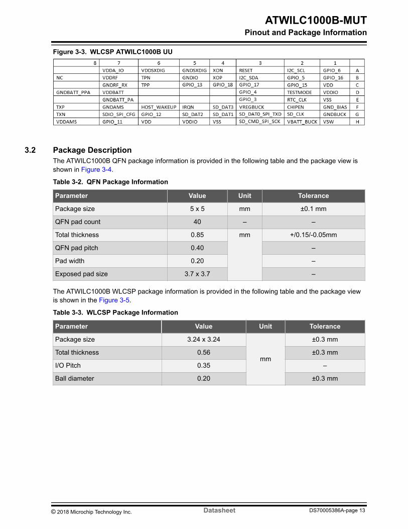
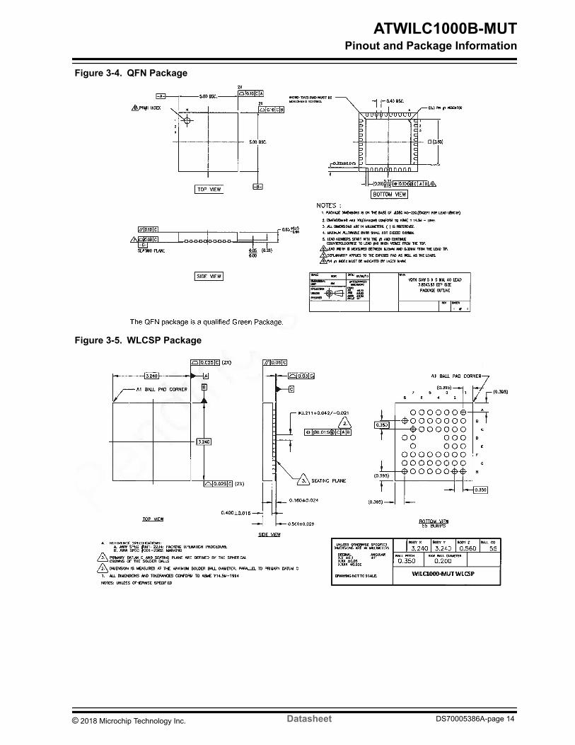
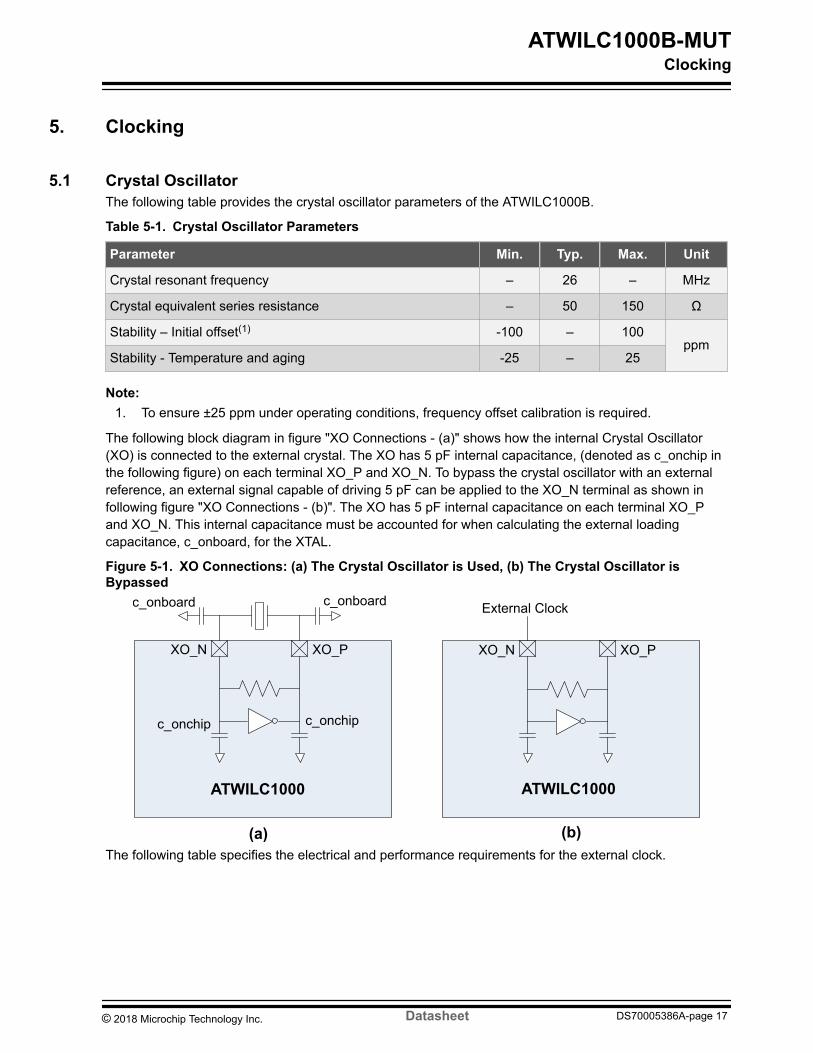
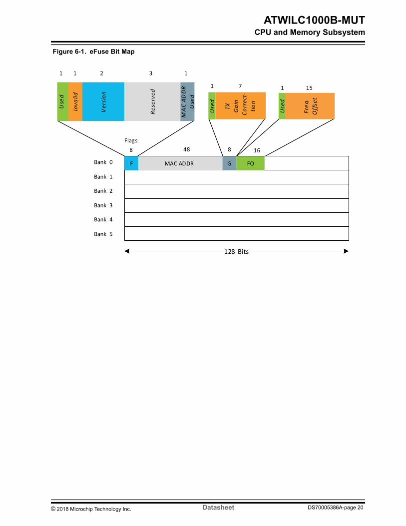
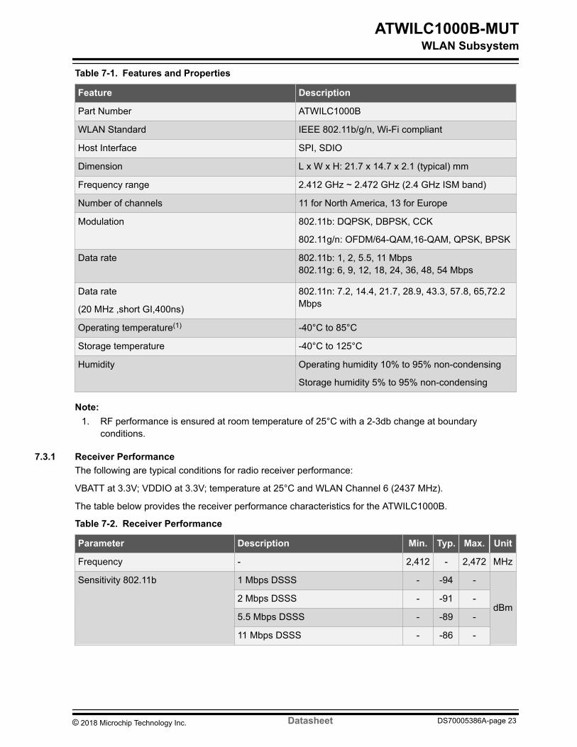
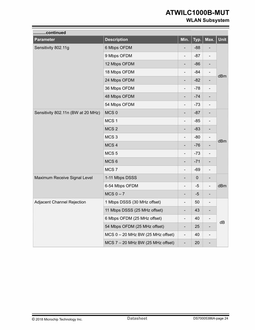
continuedParameter Description Min Typ Max Unit
Sensitivity 80211g 6 Mbps OFDM - -88 -
dBm
9 Mbps OFDM - -87 -
12 Mbps OFDM - -86 -
18 Mbps OFDM - -84 -
24 Mbps OFDM - -82 -
36 Mbps OFDM - -78 -
48 Mbps OFDM - -74 -
54 Mbps OFDM - -73 -
Sensitivity 80211n (BW at 20 MHz) MCS 0 - -87 -
dBm
MCS 1 - -85 -
MCS 2 - -83 -
MCS 3 - -80 -
MCS 4 - -76 -
MCS 5 - -73 -
MCS 6 - -71 -
MCS 7 - -69 -
Maximum Receive Signal Level 1-11 Mbps DSSS - 0 -
dBm6-54 Mbps OFDM - -5 -
MCS 0 ndash 7 - -5 -
Adjacent Channel Rejection 1 Mbps DSSS (30 MHz offset) - 50 -
dB
11 Mbps DSSS (25 MHz offset) - 43 -
6 Mbps OFDM (25 MHz offset) - 40 -
54 Mbps OFDM (25 MHz offset) - 25 -
MCS 0 ndash 20 MHz BW (25 MHz offset) - 40 -
MCS 7 ndash 20 MHz BW (25 MHz offset) - 20 -
ATWILC1000B-MUTWLAN Subsystem
copy 2018 Microchip Technology Inc Datasheet DS70005386A-page 24
continuedParameter Description Min Typ Max Unit
Cellular Blocker Immunity 776-794 MHz CDMA - -14 -
dBm
824-849 MHz GSM - -10 -
880-915 MHz GSM - -10 -
1710-1785 MHz GSM - -15 -
1850-1910 MHz GSM - -15 -
1850-1910 MHz WCDMA - -24 -
1920-1980 MHz WCDMA - -24 -
732 Transmitter PerformanceThe following are typical conditions for radio transmitter performance
VBAT=33V VDDIO=33V temperature at 25degC and WLAN Channel 6 (2437 MHz)
The following table provides the transmitter performance characteristics for the ATWILC1000B
Table 7-3 Transmitter Performance
Parameter Description Min Typ Max Unit
Frequency - 2412 2472 MHz
Output power(1)-(2)ON_Transmit
80211b 1Mbps - 176 -
dBm
80211b 11Mbps - 182 -
80211g 6Mbps - 187 -
80211g 54Mbps - 167 -
80211n MCS 0 - 173 -
80211n MCS 7 - 138 -
TX power accuracy - - plusmn15 (2) dB
Carrier suppression 80211b mode - -194 -
dBc80211g mode - -275 -
80211n mode - -211 -
ATWILC1000B-MUTWLAN Subsystem
copy 2018 Microchip Technology Inc Datasheet DS70005386A-page 25
continuedParameter Description Min Typ Max Unit
Out of band Transmit Power 76-108 - -125 -
dBmHz
776-794 - -125 -
869-960 - -125 -
925-960 - -125 -
1570-1580 - -125 -
1805-1880 - -125 -
1930-1990 - -125 -
2110-2170 - -125 -
Harmonic output power(4) 2nd - -28 -
dBmMHz3rd - -33 -
4th - -40 -
5th - -28 -
Note 1 Measured at 80211 specification compliant EVMSpectral mask2 Measured after RF matching network3 Operating temperature range is -40ordmC to +85ordmC RF performance is ensured at a room temperature
range of 25ordmC with 2-3dB change at boundary conditions4 Measured at 11 Mbps DG (Digital Gain) = -7 WLAN Channel 6 (2437 MHz)5 With respect to TX power different (higherlower) RF output power settings may be used for
specific antennas andor enclosures in which case re-certification may be required6 The availability of some specific channels andor operational frequency bands are country
dependent and should be programmed at the host product factory to match the intendeddestination Regulatory bodies prohibit exposing the settings to the end user This requirementneeds to be taken care of via host implementation
ATWILC1000B-MUTWLAN Subsystem
copy 2018 Microchip Technology Inc Datasheet DS70005386A-page 26
8 External InterfacesThe ATWILC1000B external interfaces include
bull I2C slave for controlbull SPI slave and SDIO slave for control and data transferbull SPI master for external Flashbull I2C master for external EEPROMbull UART Debug Interfacebull General Purpose InputOutput (GPIO) pins
81 I2C Slave InterfaceThe I2C Slave interface used primarily for control by the host processor is a two-wire serial interfaceconsisting of a serial data line (SDA Pin 33) and a serial clock (SCL pin 32) It responds to the seven bitaddress value 0x60 The ATWILC1000B I2C supports I2C bus Version 21 - 2000 and can operate inStandard mode (with data rates up to 100 Kbs) and Fast mode (with data rates up to 400 Kbs) The I2CSlave is a synchronous serial interface The SDA line is a bidirectional signal and changes only while theSCL line is low except for STOP START and RESTART conditions The output drivers are open-drain toperform wire-AND functions on the bus The maximum number of devices on the bus is limited by onlythe maximum capacitance specification of 400 pF Data is transmitted in byte packages For specificinformation refer to the Philips Specification entitled ldquoThe I2C -Bus Specification Version 21rdquo The I2CSlave timing is provided in the following figure
Figure 8-1 I2C Slave Timing Diagram
tHL
SDA
SCL tHDSTA
tWL
tWH
tSUDAT tPR tHDDAT
tPR tPR
tLH tHL
tLH
tSUSTOtBUF
tSUSTAfSCL
The I2C Slave timing parameters are provided in the following table
Table 8-1 I2C Slave Timing Parameters
Parameter Symbol Min Max Unit Remarks
SCL clock frequency fSCL 0 400 kHz ndash
SCL low pulse width tWL 13 ndashmicros
ndash
SCL high pulse width tWH 06 ndash ndash
ATWILC1000B-MUTExternal Interfaces
copy 2018 Microchip Technology Inc Datasheet DS70005386A-page 27
continuedParameter Symbol Min Max Unit Remarks
SCL SDA fall time tHL ndash 300ns
ndash
SCL SDA rise time tLH ndash 300 This is dictated by externalcomponents
START setup time tSUSTA 06 ndashmicros
ndash
START hold time tHDSTA 06 ndash ndash
SDA setup time tSUDAT 100 ndash
ns
ndash
SDA hold time tHDDAT 0
40
ndash Slave and master default masterprogramming option
STOP setup time tSUSTO 06 ndashmicros
ndash
Bus free time between STOP and START tBUF 13 ndash ndash
Glitch pulse reject tPR 0 50 ns ndash
82 I2C Master InterfaceThe ATWILC1000B provides an I2C bus master which is intended primarily for accessing an externalEEPROM memory through a software-defined protocol The I2C Master is a two-wire serial interfaceconsisting of a serial data line (SDA) and a serial clock line (SCL) SDA can be configured on one of thefollowing pins SD_CLK (pin 19) GPIO1 (pin 24) GPIO6 (pin 31) or I2C_SDA (pin 33) SCL can beconfigured on one of the following pins GPIO0 (pin 10) SD_DAT3 (pin 12) GPIO4 (pin 29) or I2C_SCL(pin 32) For more specific instructions refer to the ATWILC1000 Programming Guide
The I2C master interface supports three speeds
bull Standard mode (100 kbs)bull Fast mode (400 kbs)bull High-Speed mode (34 Mbs)
The timing diagram of the I2C master interface is the same as that of the I2C slave interface (see Figure8-1) The timing parameters of I2C master are shown in the following table
Table 8-2 I2C Master Timing Parameters
Parameter Symbol Standard Mode Fast Mode High-Speed Mode Unit
Min Max Min Max Min Max
SCL clock frequency fSCL 0 100 0 400 0 3400 kHz
SCL high pulse width tWH 4 ndash 06 ndash 006 ndashmicros
SCL low pulse width tWL 47 ndash 13 ndash 016 ndash
ATWILC1000B-MUTExternal Interfaces
copy 2018 Microchip Technology Inc Datasheet DS70005386A-page 28
continuedParameter Symbol Standard Mode Fast Mode High-Speed Mode Unit
Min Max Min Max Min Max
SCL fall time tHLSCL ndash 300 ndash 300 10 40
nsSDA fall time tHLSDA ndash 300 300 10 80
SCL rise time tLHSCL ndash 1000 ndash 300 10 40
SDA rise time tLHSDA ndash 1000 ndash 300 10 80
START setup time tSUSTA 47 ndash 06 ndash 016 ndashmicros
START hold time tHDSTA 4 ndash 06 ndash 016 ndash
SDA setup time tSUDAT 250 ndash 100 ndash 10 ndashns
SDA hold time tHDDAT 5 ndash 40 ndash 0 70
STOP setup time tSUSTO 4 ndash 06 ndash 016 ndash
microsBus free time between STOP andSTART
tBUF 47 ndash 13 ndash ndash ndash
Glitch pulse reject tPR ndash ndash 0 50 ndash ndash
83 SPI Slave InterfaceThe ATWILC1000B provides a Serial Peripheral Interface (SPI) that operates as an SPI slave The SPISlave interface can be used for control and for serial IO of 80211 data The SPI Slave pins are mappedas shown in the the following table The RXD pin is same as Master Output Slave Input (MOSI) and theTXD pin is same as Master Input Slave Output (MISO) The SPI Slave is a full-duplex slave-synchronousserial interface that is available immediately following reset when pin 9 (SDIO_SPI_CFG) is tied toVDDIO
Table 8-3 SPI Slave Interface Pin Mapping
Pin Number SPI Function
9 CFG Must be tied to VDDIO
16 SSN Active Low Slave Select
18 SCK Serial Clock
13 RXD Serial Data Receive (MOSI)
17 TXD Serial Data Transmit (MISO)
When the SPI is not selected ie when SSN is high the SPI interface does not interfere with datatransfers between the serial-master and other serial-slave devices When the serial slave is not selectedits transmitted data output is buffered resulting in a high impedance drive onto the serial master receiveline
The SPI Slave interface responds to a protocol that allows an external host to read or write any register inthe chip as well as initiate DMA transfers For more details of the SPI protocol and more specificinstructions refer to the ATWILC1000 Programming Guide
ATWILC1000B-MUTExternal Interfaces
copy 2018 Microchip Technology Inc Datasheet DS70005386A-page 29
The SPI Slave interface supports four standard modes as determined by the Clock Polarity (CPOL) andClock Phase (CPHA) settings These modes are illustrated in table SPI Slave Modes and Figure 8-2 Thered lines in this figure correspond to Clock Phase = 0 and the blue lines correspond to Clock Phase = 1
Table 8-4 SPI Slave Modes
Mode CPOL CPHA
0 0 0
1 0 1
2 1 0
3 1 1
Figure 8-2 SPI Slave Clock Polarity and Clock Phase Timing
z
z z
z
SCKCPOL = 0
CPOL = 1
SSN
RXDTXD(MOSIMISO)
CPHA = 0
CPHA = 1
2 3 4 5 6 7 8
1 2 3 4 5 6 7
1
8
The SPI slave timing is provided in the following figure
ATWILC1000B-MUTExternal Interfaces
copy 2018 Microchip Technology Inc Datasheet DS70005386A-page 30
Figure 8-3 SPI Slave Timing Diagram
The SPI slave timing parameters are provided in the following table
Table 8-5 SPI Slave Timing Parameters
Parameter Symbol Min Max Unit
Clock input frequency fSCK ndash 48 MHz
Clock low pulse width tWL 15 ndash
ns
Clock high pulse width tWH 15 ndash
Clock rise time tLH ndash 10
Clock fall time tHL ndash 10
Input setup time tISU 5 ndash
Input hold time tIHD 5 ndash
Output delay tODLY 0 20
Slave select setup time tSUSSN 5 ndash
Slave select hold time tHDSSN 5 ndash
84 SPI Master InterfaceThe ATWILC1000B provides an SPI master interface for accessing external Flash memory The SPImaster pins are mapped as shown in the following table The TXD pin is same as Master Output SlaveInput (MOSI) and the RXD pin is same as Master Input Slave Output (MISO) The SPI master interfacesupports all four standard modes of clock polarity and clock phase shown in Table 8-4 External SPI Flash
ATWILC1000B-MUTExternal Interfaces
copy 2018 Microchip Technology Inc Datasheet DS70005386A-page 31
memory is accessed by a processor programming commands to the SPI master interface which in turninitiates a SPI master access to the Flash For more specific instructions refer to the ATWILC1000Programming Guide
Table 8-6 SPI Master Interface Pin Mapping
Pin Number Pin Name SPI Function
28 GPIO3 SCK Serial Clock Output
29 GPIO4 SCK Active-Low Slave Select Output
30 GPIO5 TXD Serial Data Transmit Output (MOSI)
31 GPIO6 RXD Serial Data Receive Input (MISO)
The SPI master timing is provided in the following figure
Figure 8-4 SPI Master Timing Diagram
fSCK
tWHtLH
tHL
tWL
tODLY tISU tIHD
SCK
SSNTXD
RXD
The SPI master timing parameters are provided in the following table
Table 8-7 SPI Master Timing Parameters
Parameter Symbol Min Max Unit
Clock output frequency fSCK ndash 48 MHz
Clock low pulse width tWL 5 ndash
ns
Clock high pulse width tWH 5 ndash
Clock rise time tLH ndash 5
Clock fall time tHL ndash 5
Input setup time tISU 5 ndash
Input hold time tIHD 5 ndash
Output delay tODLY 0 5
ATWILC1000B-MUTExternal Interfaces
copy 2018 Microchip Technology Inc Datasheet DS70005386A-page 32
85 SDIO Slave InterfaceThe ATWILC1000B SDIO Slave is a full speed interface The interface supports the 1-bit4-bit SDTransfer mode at the clock range of 0 to 50 MHz The host can use this interface to read and write fromany register within the chip as well as configure the ATWILC1000B for data DMA To use this interfacepin 9 (SDIO_SPI_CFG) must be grounded The SDIO slave pins are mapped as shown in the followingtable
Table 8-8 SDIO Interface Pin Mapping
Pin Number SPI Function
9 CFG Must be tied to ground
12 DAT3 Data 3
13 DAT2 Data 2
16 DAT1 Data 1
17 DAT0 Data 0
18 CMD Command
19 CLK Clock
When the SDIO card is inserted into an SDIO aware host the detection of the card will be via the meansdescribed in SDIO specification During the normal initialization and interrogation of the card by the hostthe card identifies itself as an SDIO device The host software obtains the card information in a tuple(linked list) format and determines if that cardrsquos IO function(s) are acceptable to activate If the card isacceptable it is allowed to power-up fully and start the IO function(s) built into it The SD memory cardcommunication is based on an advanced 9-pin interface (clock command four data and three powerlines) designed to operate at a maximum operating frequency of 50 MHz The SDIO slave interface hasthe following features
bull Meets SDIO card specification version 20bull Host clock rate variable between 0 to 50 MHzbull 1 bit4-bit SD bus modes supportedbull Allows card to interrupt hostbull Responds to direct readwrite (IO52) and extended readwrite (IO53) transactionsbull Supports SuspendResume operation
The SDIO slave interface timing is provided in the following figure
ATWILC1000B-MUTExternal Interfaces
copy 2018 Microchip Technology Inc Datasheet DS70005386A-page 33
Figure 8-5 SDIO Slave Timing Diagram
The SDIO slave timing parameters are provided in the following table
Table 8-9 SDIO Slave Timing Parameters
Parameter Symbol Min Max Unit
Clock input frequency fPP 0 50 MHz
Clock low pulse width tWL 10 ndash
ns
Clock high pulse width tWH 10 ndash
Clock rise time tLH ndash 10
Clock fall time tHL ndash 10
Input setup time tISU 5 ndash
Input hold time tIH 5 ndash
Output delay tODLY 0 14
86 UART Debug InterfaceATWILC1000B has a Universal Asynchronous ReceiverTransmitter (UART) interface on pin 13 SD-DATA2SPI-RxD and pin 17 SD-DATA0SPI-TXD This interface should be used only for debuggingpurposes The UART is compatible with the RS-232 standard where ATWILC1000B-MUT operates asData Terminal Equipment (DTE) It has a two-pin RXDTXD interface
The default configuration for accessing the UART interface of ATWILC1000B-MUT is as followsbull Baud rate 115200bull Data 8 bitbull Parity None
ATWILC1000B-MUTExternal Interfaces
copy 2018 Microchip Technology Inc Datasheet DS70005386A-page 34
bull Stop bit 1 bitbull Flow control None
It also has Rx and Tx FIFOs which ensures reliable high speed reception and low software overheadtransmission FIFO size is 4x8 for both Rx and Tx direction The UART has status registers that show thenumber of received characters available in the FIFO and various error conditions in addition it has theability to generate interrupts based on these status bits
An example of UART receiving or transmitting a single packet is shown in the following figure Thisexample shows 7-bit data (0x45) odd parity and two stop bits
Figure 8-6 Example of UART RX or TX Packet
87 GPIOsNine General Purpose InputOutput (GPIO) pins labeled GPIO 0-8 are available to allow for applicationspecific functions Each GPIO pin can be programmed as an input (the value of the pin can be read bythe host or internal processor) or as an output (the output values can be programmed by the host orinternal processor) where the default mode after power-up is input GPIOs 7 and 8 are only availablewhen the host does not use the SDIO interface which shares two of its pins with these GPIOs Thereforefor SDIO-based applications seven GPIOs (0-6) are available For more specific usage instructions referto the ATWILC1000 Programming Guide
ATWILC1000B-MUTExternal Interfaces
copy 2018 Microchip Technology Inc Datasheet DS70005386A-page 35
9 Power Management
91 Power ArchitectureThe ATWILC1000B uses an innovative power architecture to eliminate the need for external regulatorsand reduce the number of off-chip components This architecture is shown in the following figure ThePower Management Unit (PMU) has a DCDC Converter that converts VBATT to the core supply used bythe digital and RFAMS blocks The PA and eFuse are supplied by dedicated LDOs and the VCO issupplied by a separate LDO structure The power connections in the following figure provide a conceptualframework for understanding the ATWILC1000B power architecture
Figure 9-1 Power Architecture
VBATT _BUCKOff-Chip
LC
RFAMS Core
Sleep Osc RF
AM
S C
ore
Volta
ge
VSW
VREG_BUCK
VDD_AMS VDD_RF VDD_SXDIG
LDO1VDDIO_A VDD_VCO
LDO2
~VDD_BATT
12V
10V
CHIP_EN
EFuse LDO
SX
Digital Core
DCDC Converter
EFuse
PA
PMU
RFAMS
DigitalVDDC
Dig CoreLDO
25V
PadsVDDIO
SleepLDO
Digital Core Voltage
dcdc_ena
enaena
Vin Vout
enaena
The following table provides the typical values for the digital and RFAMS core voltages
ATWILC1000B-MUTPower Management
copy 2018 Microchip Technology Inc Datasheet DS70005386A-page 36
Table 9-1 PMU Output Voltages
Parameter Typical
RFAMS core voltage (VREG_BUCK) 135V
Digital core voltage (VDDC) 110V
Refer to the reference design for an example of power supply connections including proper isolation ofthe supplies used by the digital and RFAMS blocks
92 Power ConsumptionThe ATWILC1000B has several device states
bull ON_Transmit ndash Device is actively transmitting an 80211 signalbull ON_Receive ndash Device is actively receiving an 80211 signalbull ON_Doze ndash Device is on but is neither transmitting nor receivingbull Power_Down ndash Device core supply off (leakage)
The following pins are used to switch between the ON and Power_Down statesbull CHIP_EN ndash Device pin (pin 23) used to enable DCDC Converterbull VDDIO ndash IO supply voltage from external supply
In the ON states VDDIO is on and CHIP_EN is high (at VDDIO voltage level) To switch between the ONstates and Power_Down state CHIP_EN has to change between high and low (GND) voltage WhenVDDIO is off and CHIP_EN is low the chip is powered off with no leakage (also see 93 Power-UpDownSequence)
921 Current Consumption in Various Device StatesThe following table provides the ATWILC1000B current consumption in various device states
Table 9-2 Current Consumption
Device State Code Rate Output Power(dBm)
Current Consumption(1)
IVBATT IVDDIO
ON_Transmit 80211b 1 Mbps 176 266 mA 22 mA
80211b 11 Mbps 185 239 mA 22 mA
80211g 6 Mbps 186 249 mA 22 mA
80211g 54 Mbps 169 173 mA 22 mA
80211n MCS 0 177 253 mA 22 mA
80211n MCS 7 140 164 mA 22 mA
ATWILC1000B-MUTPower Management
copy 2018 Microchip Technology Inc Datasheet DS70005386A-page 37
continuedDevice State Code Rate Output Power
(dBm)Current Consumption(1)
IVBATT IVDDIO
ON_Receive 80211b 1 Mbps NA 63 mA 22 mA
80211b 11 Mbps NA 63 mA 22 mA
80211g 6 Mbps NA 63 mA 22 mA
80211g 54 Mbps NA 63 mA 22 mA
80211n MCS 0 NA 63 mA 22 mA
80211n MCS 7 NA 63 mA 22 mA
ON_Doze NA NA 380 microA lt10 microA
Power_Down NA NA 125 μA (2)
Note 1 The power consumption values are measured when VBAT is 36V and VDDIO is 28V at 25degC
922 Controlling the Device StatesTable Device States shows how to switch between the device states using the following
bull CHIP_EN ndash Device pin (pin 23) used to enable DCDC Converterbull VDDIO ndash IO supply voltage from external supply
Table 9-3 Device States
Device State CHIP_EN VDDIO Power Consumption (1) (2)
IVBATT IVDDIO
ON_Transmit VDDIO On 172mA 18dBm (le18Mbps)
230mA 18dBm (gt18Mbps)
2mA
ON_Receive VDDIO On 60mA 2mA
ON_Doze VDDIO ON 280μA lt10μA
Power_Down GND On lt05μA lt02μA
Note 1 Conditions VBAT 36v IO18V2 Power consumption numbers are preliminary
923 Restrictions for Power StatesWhen no power is supplied to the device ie the DCDC converter output and VDDIO are both off (atground potential) In this case a voltage cannot be applied to the device pins because each pin containsan ESD diode from the pin to supply This diode turns on when voltage higher than one diode-drop issupplied to the pin
If a voltage must be applied to the signal pads while the chip is in a low power state the VDDIO supplymust be on so the SLEEP or Power_Down state must be used
ATWILC1000B-MUTPower Management
copy 2018 Microchip Technology Inc Datasheet DS70005386A-page 38
Similarly to prevent the pin-to-ground diode from turning on do not apply a voltage that is more than onediode-drop below ground to any pin
93 Power-UpDown SequenceThe power-updown sequence for the ATWILC1000B is shown in the following figure
Figure 9-2 Power-UpDown Sequence
VBATT
VDDIO
CHIP_EN
RESETN
tBIO
t IOCE
tCER
XO Clock
The timing parameters are provided in the following table
Table 9-4 Power-UpDown Sequence Timing
Parameter Min Max Unit Description Notes
tA 0 ndash
ms
VBATT rise to VDDIOrise
VBATT and VDDIO can rise simultaneously orcan be tied together VDDIO must not risebefore VBATT
tB 0 ndash VDDIO rise toCHIP_EN rise
CHIP_EN must not rise before VDDIOCHIP_EN must be driven high or low not leftfloating
tC 5 ndash CHIP_EN rise toRESETN rise
This delay is needed because XO clock muststabilize before RESETN removal RESETNmust be driven high or low not left floating
tA 0 ndash VDDIO fall to VBATTfall
VBATT and VDDIO can fall simultaneously orcan be tied together VBATT must not fall beforeVDDIO
tB 0 ndash CHIP_EN fall to VDDIOfall
VDDIO must not fall before CHIP_ENCHIP_EN and RESETN can fall simultaneously
tC 0 ndash RESETN fall to VDDIOfall
VDDIO must not fall before RESETN RESETNand CHIP_EN can fall simultaneously
ATWILC1000B-MUTPower Management
copy 2018 Microchip Technology Inc Datasheet DS70005386A-page 39
94 Digital IO Pin Behavior During Power-up SequencesThe following table represents digital IO pin states corresponding to device power modes
Table 9-5 Digital IO Pin Behavior in Different Device States
Device State VDDIO CHIP_EN RESETN Output Driver InputDriver
Pull-UpDownResistor (96kΩ)
Power_Down
core supply off
High Low Low Disabled (Hi-Z) Disabled Disabled
Power-On Reset
core supply on hardreset on
High High Low Disabled (Hi-Z) Disabled Enabled
Power-On Default
core supply on deviceout of reset but notprogrammed yet
High High High Disabled (Hi-Z) Enabled Enabled
On_DozeOn_TransmitOn_Receive
core supply on deviceprogrammed byfirmware
High High High Programmed byfirmware for eachpin
Enabled orDisabled
Oppositeof outputdriver state
Programmed byfirmware foreach pin
Enabled orDisabled
ATWILC1000B-MUTPower Management
copy 2018 Microchip Technology Inc Datasheet DS70005386A-page 40
10 Reference DesignThe ATWILC1000B reference design schematic is shown in the following figure
Figure 10-1 ATWILC1000B Reference Schematic
47u
F
22u
H
Not
e1
Add
Tes
t poi
nts
for I
2C_S
CL
and
I2C
_SD
A pi
ns2
Add
Tes
t poi
nts
for U
ART
TxD
and
RxD
pin
s
22u
H
ATWILC1000B-MUTReference Design
copy 2018 Microchip Technology Inc Datasheet DS70005386A-page 41
11 Reflow Profile InformationThis section provides the guidelines for the reflow process to get ATWILC1000B soldered to thecustomers design
111 Storage Condition
1111 Moisture Barrier Bag Before OpeningA moisture barrier bag must be stored in a temperature of less than 30degC with humidity under 85 RHThe calculated shelf life for the dry-packed product shall be 12 months from the date the bag is sealed
1112 Moisture Barrier Bag OpenHumidity indicator cards must be blue indicating that the humidity is lt30
112 Solder PasteSnAgCu eutectic solder with melting temperature of 217degC is most commonly used for lead-free solderreflow application This alloy is widely accepted in the semiconductor industry due to its low costrelatively low melting temperature and good thermal fatigue resistance Some recommended pastesinclude NC-SMQreg 230 flux and Indalloyreg 241 solder paste made up of 955 Sn38 Ag07 Cu or SENJUN705-GRN3360-K2-V Type 3 no clean paste
113 Stencil DesignThe recommended stencil is laser-cut stainless-steel type with thickness of 100 microm to 130 microm andapproximately a 11 ratio of stencil opening to pad dimension To improve paste release a positive taperwith bottom opening 25 microm larger than the top is utilized Local manufacturing experience may find othercombinations of stencil thickness and aperture size to get good results
114 Printing ProcessThe printing process requires no significant changes compared to SnPb solder Any guidelinesrecommended by the paste manufacturers to accommodate paste specific characteristics should befollowed Post-print inspection and paste volume measurement is very critical to ensure good print qualityand uniform paste
115 Baking ConditionsATWILC1000B is rated at MSL level 3 After the sealed bag is opened no baking is required within 168hours as long as the devices are held at le 30degC60 RH or stored at lt 10 RH
ATWILC1000B requires baking before mounting ifbull The sealed bag has been open for more than 168 hoursbull The humidity indicator card reads more than 10bull SIPs need to be baked for eight hours at 125degC
ATWILC1000B-MUTReflow Profile Information
copy 2018 Microchip Technology Inc Datasheet DS70005386A-page 42
116 Soldering and Reflow ConditionOptimization of the reflow process is the most critical factor considered for lead-free soldering Thedevelopment of an optimal profile must account the paste characteristics the size of the board thedensity of the components the mix of the larger and smaller components and the peak temperaturerequirements of the components An optimized reflow process is the key to ensuring a successful lead-free assembly and achieves high yield and long-term solder joint reliability
Temperature ProfilingTemperature profiling must be performed for all new board designs by attaching thermocouples at thesolder joints on the top surface of the larger components and at multiple locations of the boards This isto ensure that all components are heated to a temperature above the minimum reflow temperatures andthe smaller components do not exceed the maximum temperature limit The SnAgCu solder alloy melts at~217degC so the reflow temperature peak at joint level must be 15 to 20degC higher than meltingtemperature The targeted solder joint temperature for the SnAgCu solder must be ~235degC For larger orsophisticated boards with a large mix of components it is also important to ensure that the temperaturedifference across the board is less than 10 degrees to minimize board warpage The maximumtemperature at the component body must not exceed the MSL3 qualification specification
1161 Reflow OvenIt is strongly recommended that a reflow oven equipped with more heating zones and Nitrogenatmosphere be used for lead-free assembly Nitrogen atmosphere has shown to improve the wet-abilityand reduce temperature gradient across the board It can also enhance the appearance of the solderjoints by reducing the effects of oxidation
The following items should also be observed in the reflow process1 Some recommended pastes include
ndash NC-SMQreg 230 flux and Indalloyreg 241 solder paste made up of 955 Sn38 Ag07 Cundash SENJU N705-GRN3360-K2-V Type 3 no clean paste
2 Allowable reflow soldering iterationsndash Three times based on the following reflow soldering profile (refer following Figure)
3 Temperature profilendash Reflow soldering shall be done according to the following temperature profile (refer to the
following figure)ndash Peak temperature 250degC
ATWILC1000B-MUTReflow Profile Information
copy 2018 Microchip Technology Inc Datasheet DS70005386A-page 43
Figure 11-1 Solder Reflow Profile
Cleaning
The exposed ground paddle helps to self-align ATWILC1000B avoiding pad misalignment The use ofno-clean solder pastes is recommended Full drying of no-clean paste fluxes must be ensured as a resultof the reflow process This may require longer reflow profiles andor peak temperatures toward the highend of the process window as recommended by the solder paste vendor It is believed that uncured fluxresidues could lead to corrosion andor shorting in accelerated testing and possibly the field
Rework
Rework is to remove the mounted SIP package and replace with a new unit It is recommended that onceATWILC1000B has been removed it should never be reused During the rework process the mountedATWILC1000B and PCB are heated partially and ATWILC1000B is removed It is recommended to heat-proof the proximity of the mounted parts and junctions and use the best nozzle for rework that is suited tothe module size
ATWILC1000B-MUTReflow Profile Information
copy 2018 Microchip Technology Inc Datasheet DS70005386A-page 44
12 Reference Documentation and SupportThe following table provides the set of collateral documents to ease integration and device ramp
Table 12-1 Reference Documents
Title Content
Design FilesPackage
User Guide Schematic PCB layout Gerber BOM and System notes on RFRadio Full Test Report radiation pattern design guidelines temperatureperformance ESD
Platform Gettingstarted Guide
How-to-use package Out of the Box starting guide HW limitations and notes SWQuick start guidelines
HW Design Guide Best practices and recommendations to design a board with the product includingAntenna Design for Wi-Fi (layout recommendations types of antennas impedancematching using a power amplifier etc) SPIUART protocol between Wi-Fi SoCand the Host MCU
SW Design Guide Integration guide with clear description of High level Arch overview on how towrite a networking application list all API parameters and structures
Features of the device SPIhandshake protocol between device and host MCUflowsequence state diagram and timing
SW ProgrammerGuide
Explains in detail the flow chart and how to use each API to implement all genericuse cases (eg start AP start STA provisioning UDP TCP http TLS p2p errorsmanagement connectiontransfer recovery mechanismstate diagram) ndash usageand sample application note
For a complete listing of development-support tools and documentation visit the ATWILC1000 webpageor refer to the customer support section on options to contact the nearest Microchip field representative
ATWILC1000B-MUTReference Documentation and Support
copy 2018 Microchip Technology Inc Datasheet DS70005386A-page 45
13 Document Revision HistoryRevision Date Section Description
A 122018 Document bull Updated from Atmelto Microchiptemplate
bull Assigned a newMicrochip documentnumber Previousversion is Atmel42351 revision D
bull ISBN numberadded
Document Revision History-Atmel
Doc Rev Date Comments
42351D 052015 DS update to Rev B offering
Changes from ATWILC1000A to ATWILC1000B
1 Added second UART increased UART data rates2 Increased instruction RAM size from 128KB to 160KB3 Updated pin MUX table added new options for various interfaces4 Improved description of Coexistence interface5 Added VDD_VCO switch and connection in the power architecture6 Updated power consumption numbers7 Updated reference schematic8 Changed RTC_CLK pad definition from pull-down to pull-up
42351C 022015 DS update new Atmel format
42351B 112014 Major document update new sections added replaced text in most sections newand updated drawings
42351A 072014 Initial document release
ATWILC1000B-MUTDocument Revision History
copy 2018 Microchip Technology Inc Datasheet DS70005386A-page 46
The Microchip Web Site
Microchip provides online support via our web site at httpwwwmicrochipcom This web site is used asa means to make files and information easily available to customers Accessible by using your favoriteInternet browser the web site contains the following information
bull Product Support ndash Data sheets and errata application notes and sample programs designresources userrsquos guides and hardware support documents latest software releases and archivedsoftware
bull General Technical Support ndash Frequently Asked Questions (FAQ) technical support requests onlinediscussion groups Microchip consultant program member listing
bull Business of Microchip ndash Product selector and ordering guides latest Microchip press releaseslisting of seminars and events listings of Microchip sales offices distributors and factoryrepresentatives
Customer Change Notification Service
Microchiprsquos customer notification service helps keep customers current on Microchip productsSubscribers will receive e-mail notification whenever there are changes updates revisions or erratarelated to a specified product family or development tool of interest
To register access the Microchip web site at httpwwwmicrochipcom Under ldquoSupportrdquo click onldquoCustomer Change Notificationrdquo and follow the registration instructions
Customer Support
Users of Microchip products can receive assistance through several channels
bull Distributor or Representativebull Local Sales Officebull Field Application Engineer (FAE)bull Technical Support
Customers should contact their distributor representative or Field Application Engineer (FAE) for supportLocal sales offices are also available to help customers A listing of sales offices and locations is includedin the back of this document
Technical support is available through the web site at httpwwwmicrochipcomsupport
Microchip Devices Code Protection Feature
Note the following details of the code protection feature on Microchip devices
bull Microchip products meet the specification contained in their particular Microchip Data Sheetbull Microchip believes that its family of products is one of the most secure families of its kind on the
market today when used in the intended manner and under normal conditionsbull There are dishonest and possibly illegal methods used to breach the code protection feature All of
these methods to our knowledge require using the Microchip products in a manner outside theoperating specifications contained in Microchiprsquos Data Sheets Most likely the person doing so isengaged in theft of intellectual property
bull Microchip is willing to work with the customer who is concerned about the integrity of their code
ATWILC1000B-MUT
copy 2018 Microchip Technology Inc Datasheet DS70005386A-page 47
bull Neither Microchip nor any other semiconductor manufacturer can guarantee the security of theircode Code protection does not mean that we are guaranteeing the product as ldquounbreakablerdquo
Code protection is constantly evolving We at Microchip are committed to continuously improving thecode protection features of our products Attempts to break Microchiprsquos code protection feature may be aviolation of the Digital Millennium Copyright Act If such acts allow unauthorized access to your softwareor other copyrighted work you may have a right to sue for relief under that Act
Legal Notice
Information contained in this publication regarding device applications and the like is provided only foryour convenience and may be superseded by updates It is your responsibility to ensure that yourapplication meets with your specifications MICROCHIP MAKES NO REPRESENTATIONS ORWARRANTIES OF ANY KIND WHETHER EXPRESS OR IMPLIED WRITTEN OR ORAL STATUTORYOR OTHERWISE RELATED TO THE INFORMATION INCLUDING BUT NOT LIMITED TO ITSCONDITION QUALITY PERFORMANCE MERCHANTABILITY OR FITNESS FOR PURPOSEMicrochip disclaims all liability arising from this information and its use Use of Microchip devices in lifesupport andor safety applications is entirely at the buyerrsquos risk and the buyer agrees to defendindemnify and hold harmless Microchip from any and all damages claims suits or expenses resultingfrom such use No licenses are conveyed implicitly or otherwise under any Microchip intellectualproperty rights unless otherwise stated
Trademarks
The Microchip name and logo the Microchip logo AnyRate AVR AVR logo AVR Freaks BitCloudchipKIT chipKIT logo CryptoMemory CryptoRF dsPIC FlashFlex flexPWR Heldo JukeBlox KeeLoqKleer LANCheck LINK MD maXStylus maXTouch MediaLB megaAVR MOST MOST logo MPLABOptoLyzer PIC picoPower PICSTART PIC32 logo Prochip Designer QTouch SAM-BA SpyNIC SSTSST Logo SuperFlash tinyAVR UNIO and XMEGA are registered trademarks of Microchip TechnologyIncorporated in the USA and other countries
ClockWorks The Embedded Control Solutions Company EtherSynch Hyper Speed Control HyperLightLoad IntelliMOS mTouch Precision Edge and Quiet-Wire are registered trademarks of MicrochipTechnology Incorporated in the USA
Adjacent Key Suppression AKS Analog-for-the-Digital Age Any Capacitor AnyIn AnyOut BodyComCodeGuard CryptoAuthentication CryptoAutomotive CryptoCompanion CryptoController dsPICDEMdsPICDEMnet Dynamic Average Matching DAM ECAN EtherGREEN In-Circuit Serial ProgrammingICSP INICnet Inter-Chip Connectivity JitterBlocker KleerNet KleerNet logo memBrain Mindi MiWimotorBench MPASM MPF MPLAB Certified logo MPLIB MPLINK MultiTRAK NetDetach OmniscientCode Generation PICDEM PICDEMnet PICkit PICtail PowerSmart PureSilicon QMatrix REAL ICERipple Blocker SAM-ICE Serial Quad IO SMART-IS SQI SuperSwitcher SuperSwitcher II TotalEndurance TSHARC USBCheck VariSense ViewSpan WiperLock Wireless DNA and ZENA aretrademarks of Microchip Technology Incorporated in the USA and other countries
SQTP is a service mark of Microchip Technology Incorporated in the USA
Silicon Storage Technology is a registered trademark of Microchip Technology Inc in other countries
GestIC is a registered trademark of Microchip Technology Germany II GmbH amp Co KG a subsidiary ofMicrochip Technology Inc in other countries
All other trademarks mentioned herein are property of their respective companies
ATWILC1000B-MUT
copy 2018 Microchip Technology Inc Datasheet DS70005386A-page 48
copy 2018 Microchip Technology Incorporated Printed in the USA All Rights Reserved
ISBN 978-1-5224-3998-1
Quality Management System Certified by DNV
ISOTS 16949Microchip received ISOTS-169492009 certification for its worldwide headquarters design and waferfabrication facilities in Chandler and Tempe Arizona Gresham Oregon and design centers in Californiaand India The Companyrsquos quality system processes and procedures are for its PICreg MCUs and dsPICreg
DSCs KEELOQreg code hopping devices Serial EEPROMs microperipherals nonvolatile memory andanalog products In addition Microchiprsquos quality system for the design and manufacture of developmentsystems is ISO 90012000 certified
ATWILC1000B-MUT
copy 2018 Microchip Technology Inc Datasheet DS70005386A-page 49
AMERICAS ASIAPACIFIC ASIAPACIFIC EUROPECorporate Office2355 West Chandler BlvdChandler AZ 85224-6199Tel 480-792-7200Fax 480-792-7277Technical SupporthttpwwwmicrochipcomsupportWeb AddresswwwmicrochipcomAtlantaDuluth GATel 678-957-9614Fax 678-957-1455Austin TXTel 512-257-3370BostonWestborough MATel 774-760-0087Fax 774-760-0088ChicagoItasca ILTel 630-285-0071Fax 630-285-0075DallasAddison TXTel 972-818-7423Fax 972-818-2924DetroitNovi MITel 248-848-4000Houston TXTel 281-894-5983IndianapolisNoblesville INTel 317-773-8323Fax 317-773-5453Tel 317-536-2380Los AngelesMission Viejo CATel 949-462-9523Fax 949-462-9608Tel 951-273-7800Raleigh NCTel 919-844-7510New York NYTel 631-435-6000San Jose CATel 408-735-9110Tel 408-436-4270Canada - TorontoTel 905-695-1980Fax 905-695-2078
Australia - SydneyTel 61-2-9868-6733China - BeijingTel 86-10-8569-7000China - ChengduTel 86-28-8665-5511China - ChongqingTel 86-23-8980-9588China - DongguanTel 86-769-8702-9880China - GuangzhouTel 86-20-8755-8029China - HangzhouTel 86-571-8792-8115China - Hong Kong SARTel 852-2943-5100China - NanjingTel 86-25-8473-2460China - QingdaoTel 86-532-8502-7355China - ShanghaiTel 86-21-3326-8000China - ShenyangTel 86-24-2334-2829China - ShenzhenTel 86-755-8864-2200China - SuzhouTel 86-186-6233-1526China - WuhanTel 86-27-5980-5300China - XianTel 86-29-8833-7252China - XiamenTel 86-592-2388138China - ZhuhaiTel 86-756-3210040
India - BangaloreTel 91-80-3090-4444India - New DelhiTel 91-11-4160-8631India - PuneTel 91-20-4121-0141Japan - OsakaTel 81-6-6152-7160Japan - TokyoTel 81-3-6880- 3770Korea - DaeguTel 82-53-744-4301Korea - SeoulTel 82-2-554-7200Malaysia - Kuala LumpurTel 60-3-7651-7906Malaysia - PenangTel 60-4-227-8870Philippines - ManilaTel 63-2-634-9065SingaporeTel 65-6334-8870Taiwan - Hsin ChuTel 886-3-577-8366Taiwan - KaohsiungTel 886-7-213-7830Taiwan - TaipeiTel 886-2-2508-8600Thailand - BangkokTel 66-2-694-1351Vietnam - Ho Chi MinhTel 84-28-5448-2100
Austria - WelsTel 43-7242-2244-39Fax 43-7242-2244-393Denmark - CopenhagenTel 45-4450-2828Fax 45-4485-2829Finland - EspooTel 358-9-4520-820France - ParisTel 33-1-69-53-63-20Fax 33-1-69-30-90-79Germany - GarchingTel 49-8931-9700Germany - HaanTel 49-2129-3766400Germany - HeilbronnTel 49-7131-67-3636Germany - KarlsruheTel 49-721-625370Germany - MunichTel 49-89-627-144-0Fax 49-89-627-144-44Germany - RosenheimTel 49-8031-354-560Israel - RarsquoananaTel 972-9-744-7705Italy - MilanTel 39-0331-742611Fax 39-0331-466781Italy - PadovaTel 39-049-7625286Netherlands - DrunenTel 31-416-690399Fax 31-416-690340Norway - TrondheimTel 47-72884388Poland - WarsawTel 48-22-3325737Romania - BucharestTel 40-21-407-87-50Spain - MadridTel 34-91-708-08-90Fax 34-91-708-08-91Sweden - GothenbergTel 46-31-704-60-40Sweden - StockholmTel 46-8-5090-4654UK - WokinghamTel 44-118-921-5800Fax 44-118-921-5820
Worldwide Sales and Service
copy 2018 Microchip Technology Inc Datasheet DS70005386A-page 50
- Introduction
- Features
- Table of Contents
- 1 Ordering Information and IC Marking
- 2 Block Diagram
- 3 Pinout and Package Information
-
- 31 Pin Description
- 32 Package Description
-
- 4 Electrical Specifications
-
- 41 Absolute Ratings
- 42 Recommended Operating Conditions
- 43 DC Electrical Characteristics
-
- 5 Clocking
-
- 51 Crystal Oscillator
- 52 Low-Power Oscillator
-
- 6 CPU and Memory Subsystem
-
- 61 Processor
- 62 Memory Subsystem
- 63 Nonvolatile Memory (eFuse)
-
- 7 WLAN Subsystem
-
- 71 MAC
-
- 711 Features
- 712 Description
-
- 72 PHY
-
- 721 Features
- 722 Description
-
- 73 Radio
-
- 731 Receiver Performance
- 732 Transmitter Performance
-
- 8 External Interfaces
-
- 81 I2C Slave Interface
- 82 I2C Master Interface
- 83 SPI Slave Interface
- 84 SPI Master Interface
- 85 SDIO Slave Interface
- 86 UART Debug Interface
- 87 GPIOs
-
- 9 Power Management
-
- 91 Power Architecture
- 92 Power Consumption
-
- 921 Current Consumption in Various Device States
- 922 Controlling the Device States
- 923 Restrictions for Power States
-
- 93 Power-UpDown Sequence
- 94 Digital IO Pin Behavior During Power-up Sequences
-
- 10 Reference Design
- 11 Reflow Profile Information
-
- 111 Storage Condition
-
- 1111 Moisture Barrier Bag Before Opening
- 1112 Moisture Barrier Bag Open
-
- 112 Solder Paste
- 113 Stencil Design
- 114 Printing Process
- 115 Baking Conditions
- 116 Soldering and Reflow Condition
-
- 1161 Reflow Oven
-
- 12 Reference Documentation and Support
- 13 Document Revision History
- The Microchip Web Site
- Customer Change Notification Service
- Customer Support
- Microchip Devices Code Protection Feature
- Legal Notice
- Trademarks
- Quality Management System Certified by DNV
- Worldwide Sales and Service
-
continuedParameter Description Min Typ Max Unit
Out of band Transmit Power 76-108 - -125 -
dBmHz
776-794 - -125 -
869-960 - -125 -
925-960 - -125 -
1570-1580 - -125 -
1805-1880 - -125 -
1930-1990 - -125 -
2110-2170 - -125 -
Harmonic output power(4) 2nd - -28 -
dBmMHz3rd - -33 -
4th - -40 -
5th - -28 -
Note 1 Measured at 80211 specification compliant EVMSpectral mask2 Measured after RF matching network3 Operating temperature range is -40ordmC to +85ordmC RF performance is ensured at a room temperature
range of 25ordmC with 2-3dB change at boundary conditions4 Measured at 11 Mbps DG (Digital Gain) = -7 WLAN Channel 6 (2437 MHz)5 With respect to TX power different (higherlower) RF output power settings may be used for
specific antennas andor enclosures in which case re-certification may be required6 The availability of some specific channels andor operational frequency bands are country
dependent and should be programmed at the host product factory to match the intendeddestination Regulatory bodies prohibit exposing the settings to the end user This requirementneeds to be taken care of via host implementation
ATWILC1000B-MUTWLAN Subsystem
copy 2018 Microchip Technology Inc Datasheet DS70005386A-page 26
8 External InterfacesThe ATWILC1000B external interfaces include
bull I2C slave for controlbull SPI slave and SDIO slave for control and data transferbull SPI master for external Flashbull I2C master for external EEPROMbull UART Debug Interfacebull General Purpose InputOutput (GPIO) pins
81 I2C Slave InterfaceThe I2C Slave interface used primarily for control by the host processor is a two-wire serial interfaceconsisting of a serial data line (SDA Pin 33) and a serial clock (SCL pin 32) It responds to the seven bitaddress value 0x60 The ATWILC1000B I2C supports I2C bus Version 21 - 2000 and can operate inStandard mode (with data rates up to 100 Kbs) and Fast mode (with data rates up to 400 Kbs) The I2CSlave is a synchronous serial interface The SDA line is a bidirectional signal and changes only while theSCL line is low except for STOP START and RESTART conditions The output drivers are open-drain toperform wire-AND functions on the bus The maximum number of devices on the bus is limited by onlythe maximum capacitance specification of 400 pF Data is transmitted in byte packages For specificinformation refer to the Philips Specification entitled ldquoThe I2C -Bus Specification Version 21rdquo The I2CSlave timing is provided in the following figure
Figure 8-1 I2C Slave Timing Diagram
tHL
SDA
SCL tHDSTA
tWL
tWH
tSUDAT tPR tHDDAT
tPR tPR
tLH tHL
tLH
tSUSTOtBUF
tSUSTAfSCL
The I2C Slave timing parameters are provided in the following table
Table 8-1 I2C Slave Timing Parameters
Parameter Symbol Min Max Unit Remarks
SCL clock frequency fSCL 0 400 kHz ndash
SCL low pulse width tWL 13 ndashmicros
ndash
SCL high pulse width tWH 06 ndash ndash
ATWILC1000B-MUTExternal Interfaces
copy 2018 Microchip Technology Inc Datasheet DS70005386A-page 27
continuedParameter Symbol Min Max Unit Remarks
SCL SDA fall time tHL ndash 300ns
ndash
SCL SDA rise time tLH ndash 300 This is dictated by externalcomponents
START setup time tSUSTA 06 ndashmicros
ndash
START hold time tHDSTA 06 ndash ndash
SDA setup time tSUDAT 100 ndash
ns
ndash
SDA hold time tHDDAT 0
40
ndash Slave and master default masterprogramming option
STOP setup time tSUSTO 06 ndashmicros
ndash
Bus free time between STOP and START tBUF 13 ndash ndash
Glitch pulse reject tPR 0 50 ns ndash
82 I2C Master InterfaceThe ATWILC1000B provides an I2C bus master which is intended primarily for accessing an externalEEPROM memory through a software-defined protocol The I2C Master is a two-wire serial interfaceconsisting of a serial data line (SDA) and a serial clock line (SCL) SDA can be configured on one of thefollowing pins SD_CLK (pin 19) GPIO1 (pin 24) GPIO6 (pin 31) or I2C_SDA (pin 33) SCL can beconfigured on one of the following pins GPIO0 (pin 10) SD_DAT3 (pin 12) GPIO4 (pin 29) or I2C_SCL(pin 32) For more specific instructions refer to the ATWILC1000 Programming Guide
The I2C master interface supports three speeds
bull Standard mode (100 kbs)bull Fast mode (400 kbs)bull High-Speed mode (34 Mbs)
The timing diagram of the I2C master interface is the same as that of the I2C slave interface (see Figure8-1) The timing parameters of I2C master are shown in the following table
Table 8-2 I2C Master Timing Parameters
Parameter Symbol Standard Mode Fast Mode High-Speed Mode Unit
Min Max Min Max Min Max
SCL clock frequency fSCL 0 100 0 400 0 3400 kHz
SCL high pulse width tWH 4 ndash 06 ndash 006 ndashmicros
SCL low pulse width tWL 47 ndash 13 ndash 016 ndash
ATWILC1000B-MUTExternal Interfaces
copy 2018 Microchip Technology Inc Datasheet DS70005386A-page 28
continuedParameter Symbol Standard Mode Fast Mode High-Speed Mode Unit
Min Max Min Max Min Max
SCL fall time tHLSCL ndash 300 ndash 300 10 40
nsSDA fall time tHLSDA ndash 300 300 10 80
SCL rise time tLHSCL ndash 1000 ndash 300 10 40
SDA rise time tLHSDA ndash 1000 ndash 300 10 80
START setup time tSUSTA 47 ndash 06 ndash 016 ndashmicros
START hold time tHDSTA 4 ndash 06 ndash 016 ndash
SDA setup time tSUDAT 250 ndash 100 ndash 10 ndashns
SDA hold time tHDDAT 5 ndash 40 ndash 0 70
STOP setup time tSUSTO 4 ndash 06 ndash 016 ndash
microsBus free time between STOP andSTART
tBUF 47 ndash 13 ndash ndash ndash
Glitch pulse reject tPR ndash ndash 0 50 ndash ndash
83 SPI Slave InterfaceThe ATWILC1000B provides a Serial Peripheral Interface (SPI) that operates as an SPI slave The SPISlave interface can be used for control and for serial IO of 80211 data The SPI Slave pins are mappedas shown in the the following table The RXD pin is same as Master Output Slave Input (MOSI) and theTXD pin is same as Master Input Slave Output (MISO) The SPI Slave is a full-duplex slave-synchronousserial interface that is available immediately following reset when pin 9 (SDIO_SPI_CFG) is tied toVDDIO
Table 8-3 SPI Slave Interface Pin Mapping
Pin Number SPI Function
9 CFG Must be tied to VDDIO
16 SSN Active Low Slave Select
18 SCK Serial Clock
13 RXD Serial Data Receive (MOSI)
17 TXD Serial Data Transmit (MISO)
When the SPI is not selected ie when SSN is high the SPI interface does not interfere with datatransfers between the serial-master and other serial-slave devices When the serial slave is not selectedits transmitted data output is buffered resulting in a high impedance drive onto the serial master receiveline
The SPI Slave interface responds to a protocol that allows an external host to read or write any register inthe chip as well as initiate DMA transfers For more details of the SPI protocol and more specificinstructions refer to the ATWILC1000 Programming Guide
ATWILC1000B-MUTExternal Interfaces
copy 2018 Microchip Technology Inc Datasheet DS70005386A-page 29
The SPI Slave interface supports four standard modes as determined by the Clock Polarity (CPOL) andClock Phase (CPHA) settings These modes are illustrated in table SPI Slave Modes and Figure 8-2 Thered lines in this figure correspond to Clock Phase = 0 and the blue lines correspond to Clock Phase = 1
Table 8-4 SPI Slave Modes
Mode CPOL CPHA
0 0 0
1 0 1
2 1 0
3 1 1
Figure 8-2 SPI Slave Clock Polarity and Clock Phase Timing
z
z z
z
SCKCPOL = 0
CPOL = 1
SSN
RXDTXD(MOSIMISO)
CPHA = 0
CPHA = 1
2 3 4 5 6 7 8
1 2 3 4 5 6 7
1
8
The SPI slave timing is provided in the following figure
ATWILC1000B-MUTExternal Interfaces
copy 2018 Microchip Technology Inc Datasheet DS70005386A-page 30
Figure 8-3 SPI Slave Timing Diagram
The SPI slave timing parameters are provided in the following table
Table 8-5 SPI Slave Timing Parameters
Parameter Symbol Min Max Unit
Clock input frequency fSCK ndash 48 MHz
Clock low pulse width tWL 15 ndash
ns
Clock high pulse width tWH 15 ndash
Clock rise time tLH ndash 10
Clock fall time tHL ndash 10
Input setup time tISU 5 ndash
Input hold time tIHD 5 ndash
Output delay tODLY 0 20
Slave select setup time tSUSSN 5 ndash
Slave select hold time tHDSSN 5 ndash
84 SPI Master InterfaceThe ATWILC1000B provides an SPI master interface for accessing external Flash memory The SPImaster pins are mapped as shown in the following table The TXD pin is same as Master Output SlaveInput (MOSI) and the RXD pin is same as Master Input Slave Output (MISO) The SPI master interfacesupports all four standard modes of clock polarity and clock phase shown in Table 8-4 External SPI Flash
ATWILC1000B-MUTExternal Interfaces
copy 2018 Microchip Technology Inc Datasheet DS70005386A-page 31
memory is accessed by a processor programming commands to the SPI master interface which in turninitiates a SPI master access to the Flash For more specific instructions refer to the ATWILC1000Programming Guide
Table 8-6 SPI Master Interface Pin Mapping
Pin Number Pin Name SPI Function
28 GPIO3 SCK Serial Clock Output
29 GPIO4 SCK Active-Low Slave Select Output
30 GPIO5 TXD Serial Data Transmit Output (MOSI)
31 GPIO6 RXD Serial Data Receive Input (MISO)
The SPI master timing is provided in the following figure
Figure 8-4 SPI Master Timing Diagram
fSCK
tWHtLH
tHL
tWL
tODLY tISU tIHD
SCK
SSNTXD
RXD
The SPI master timing parameters are provided in the following table
Table 8-7 SPI Master Timing Parameters
Parameter Symbol Min Max Unit
Clock output frequency fSCK ndash 48 MHz
Clock low pulse width tWL 5 ndash
ns
Clock high pulse width tWH 5 ndash
Clock rise time tLH ndash 5
Clock fall time tHL ndash 5
Input setup time tISU 5 ndash
Input hold time tIHD 5 ndash
Output delay tODLY 0 5
ATWILC1000B-MUTExternal Interfaces
copy 2018 Microchip Technology Inc Datasheet DS70005386A-page 32
85 SDIO Slave InterfaceThe ATWILC1000B SDIO Slave is a full speed interface The interface supports the 1-bit4-bit SDTransfer mode at the clock range of 0 to 50 MHz The host can use this interface to read and write fromany register within the chip as well as configure the ATWILC1000B for data DMA To use this interfacepin 9 (SDIO_SPI_CFG) must be grounded The SDIO slave pins are mapped as shown in the followingtable
Table 8-8 SDIO Interface Pin Mapping
Pin Number SPI Function
9 CFG Must be tied to ground
12 DAT3 Data 3
13 DAT2 Data 2
16 DAT1 Data 1
17 DAT0 Data 0
18 CMD Command
19 CLK Clock
When the SDIO card is inserted into an SDIO aware host the detection of the card will be via the meansdescribed in SDIO specification During the normal initialization and interrogation of the card by the hostthe card identifies itself as an SDIO device The host software obtains the card information in a tuple(linked list) format and determines if that cardrsquos IO function(s) are acceptable to activate If the card isacceptable it is allowed to power-up fully and start the IO function(s) built into it The SD memory cardcommunication is based on an advanced 9-pin interface (clock command four data and three powerlines) designed to operate at a maximum operating frequency of 50 MHz The SDIO slave interface hasthe following features
bull Meets SDIO card specification version 20bull Host clock rate variable between 0 to 50 MHzbull 1 bit4-bit SD bus modes supportedbull Allows card to interrupt hostbull Responds to direct readwrite (IO52) and extended readwrite (IO53) transactionsbull Supports SuspendResume operation
The SDIO slave interface timing is provided in the following figure
ATWILC1000B-MUTExternal Interfaces
copy 2018 Microchip Technology Inc Datasheet DS70005386A-page 33
Figure 8-5 SDIO Slave Timing Diagram
The SDIO slave timing parameters are provided in the following table
Table 8-9 SDIO Slave Timing Parameters
Parameter Symbol Min Max Unit
Clock input frequency fPP 0 50 MHz
Clock low pulse width tWL 10 ndash
ns
Clock high pulse width tWH 10 ndash
Clock rise time tLH ndash 10
Clock fall time tHL ndash 10
Input setup time tISU 5 ndash
Input hold time tIH 5 ndash
Output delay tODLY 0 14
86 UART Debug InterfaceATWILC1000B has a Universal Asynchronous ReceiverTransmitter (UART) interface on pin 13 SD-DATA2SPI-RxD and pin 17 SD-DATA0SPI-TXD This interface should be used only for debuggingpurposes The UART is compatible with the RS-232 standard where ATWILC1000B-MUT operates asData Terminal Equipment (DTE) It has a two-pin RXDTXD interface
The default configuration for accessing the UART interface of ATWILC1000B-MUT is as followsbull Baud rate 115200bull Data 8 bitbull Parity None
ATWILC1000B-MUTExternal Interfaces
copy 2018 Microchip Technology Inc Datasheet DS70005386A-page 34
bull Stop bit 1 bitbull Flow control None
It also has Rx and Tx FIFOs which ensures reliable high speed reception and low software overheadtransmission FIFO size is 4x8 for both Rx and Tx direction The UART has status registers that show thenumber of received characters available in the FIFO and various error conditions in addition it has theability to generate interrupts based on these status bits
An example of UART receiving or transmitting a single packet is shown in the following figure Thisexample shows 7-bit data (0x45) odd parity and two stop bits
Figure 8-6 Example of UART RX or TX Packet
87 GPIOsNine General Purpose InputOutput (GPIO) pins labeled GPIO 0-8 are available to allow for applicationspecific functions Each GPIO pin can be programmed as an input (the value of the pin can be read bythe host or internal processor) or as an output (the output values can be programmed by the host orinternal processor) where the default mode after power-up is input GPIOs 7 and 8 are only availablewhen the host does not use the SDIO interface which shares two of its pins with these GPIOs Thereforefor SDIO-based applications seven GPIOs (0-6) are available For more specific usage instructions referto the ATWILC1000 Programming Guide
ATWILC1000B-MUTExternal Interfaces
copy 2018 Microchip Technology Inc Datasheet DS70005386A-page 35
9 Power Management
91 Power ArchitectureThe ATWILC1000B uses an innovative power architecture to eliminate the need for external regulatorsand reduce the number of off-chip components This architecture is shown in the following figure ThePower Management Unit (PMU) has a DCDC Converter that converts VBATT to the core supply used bythe digital and RFAMS blocks The PA and eFuse are supplied by dedicated LDOs and the VCO issupplied by a separate LDO structure The power connections in the following figure provide a conceptualframework for understanding the ATWILC1000B power architecture
Figure 9-1 Power Architecture
VBATT _BUCKOff-Chip
LC
RFAMS Core
Sleep Osc RF
AM
S C
ore
Volta
ge
VSW
VREG_BUCK
VDD_AMS VDD_RF VDD_SXDIG
LDO1VDDIO_A VDD_VCO
LDO2
~VDD_BATT
12V
10V
CHIP_EN
EFuse LDO
SX
Digital Core
DCDC Converter
EFuse
PA
PMU
RFAMS
DigitalVDDC
Dig CoreLDO
25V
PadsVDDIO
SleepLDO
Digital Core Voltage
dcdc_ena
enaena
Vin Vout
enaena
The following table provides the typical values for the digital and RFAMS core voltages
ATWILC1000B-MUTPower Management
copy 2018 Microchip Technology Inc Datasheet DS70005386A-page 36
Table 9-1 PMU Output Voltages
Parameter Typical
RFAMS core voltage (VREG_BUCK) 135V
Digital core voltage (VDDC) 110V
Refer to the reference design for an example of power supply connections including proper isolation ofthe supplies used by the digital and RFAMS blocks
92 Power ConsumptionThe ATWILC1000B has several device states
bull ON_Transmit ndash Device is actively transmitting an 80211 signalbull ON_Receive ndash Device is actively receiving an 80211 signalbull ON_Doze ndash Device is on but is neither transmitting nor receivingbull Power_Down ndash Device core supply off (leakage)
The following pins are used to switch between the ON and Power_Down statesbull CHIP_EN ndash Device pin (pin 23) used to enable DCDC Converterbull VDDIO ndash IO supply voltage from external supply
In the ON states VDDIO is on and CHIP_EN is high (at VDDIO voltage level) To switch between the ONstates and Power_Down state CHIP_EN has to change between high and low (GND) voltage WhenVDDIO is off and CHIP_EN is low the chip is powered off with no leakage (also see 93 Power-UpDownSequence)
921 Current Consumption in Various Device StatesThe following table provides the ATWILC1000B current consumption in various device states
Table 9-2 Current Consumption
Device State Code Rate Output Power(dBm)
Current Consumption(1)
IVBATT IVDDIO
ON_Transmit 80211b 1 Mbps 176 266 mA 22 mA
80211b 11 Mbps 185 239 mA 22 mA
80211g 6 Mbps 186 249 mA 22 mA
80211g 54 Mbps 169 173 mA 22 mA
80211n MCS 0 177 253 mA 22 mA
80211n MCS 7 140 164 mA 22 mA
ATWILC1000B-MUTPower Management
copy 2018 Microchip Technology Inc Datasheet DS70005386A-page 37
continuedDevice State Code Rate Output Power
(dBm)Current Consumption(1)
IVBATT IVDDIO
ON_Receive 80211b 1 Mbps NA 63 mA 22 mA
80211b 11 Mbps NA 63 mA 22 mA
80211g 6 Mbps NA 63 mA 22 mA
80211g 54 Mbps NA 63 mA 22 mA
80211n MCS 0 NA 63 mA 22 mA
80211n MCS 7 NA 63 mA 22 mA
ON_Doze NA NA 380 microA lt10 microA
Power_Down NA NA 125 μA (2)
Note 1 The power consumption values are measured when VBAT is 36V and VDDIO is 28V at 25degC
922 Controlling the Device StatesTable Device States shows how to switch between the device states using the following
bull CHIP_EN ndash Device pin (pin 23) used to enable DCDC Converterbull VDDIO ndash IO supply voltage from external supply
Table 9-3 Device States
Device State CHIP_EN VDDIO Power Consumption (1) (2)
IVBATT IVDDIO
ON_Transmit VDDIO On 172mA 18dBm (le18Mbps)
230mA 18dBm (gt18Mbps)
2mA
ON_Receive VDDIO On 60mA 2mA
ON_Doze VDDIO ON 280μA lt10μA
Power_Down GND On lt05μA lt02μA
Note 1 Conditions VBAT 36v IO18V2 Power consumption numbers are preliminary
923 Restrictions for Power StatesWhen no power is supplied to the device ie the DCDC converter output and VDDIO are both off (atground potential) In this case a voltage cannot be applied to the device pins because each pin containsan ESD diode from the pin to supply This diode turns on when voltage higher than one diode-drop issupplied to the pin
If a voltage must be applied to the signal pads while the chip is in a low power state the VDDIO supplymust be on so the SLEEP or Power_Down state must be used
ATWILC1000B-MUTPower Management
copy 2018 Microchip Technology Inc Datasheet DS70005386A-page 38
Similarly to prevent the pin-to-ground diode from turning on do not apply a voltage that is more than onediode-drop below ground to any pin
93 Power-UpDown SequenceThe power-updown sequence for the ATWILC1000B is shown in the following figure
Figure 9-2 Power-UpDown Sequence
VBATT
VDDIO
CHIP_EN
RESETN
tBIO
t IOCE
tCER
XO Clock
The timing parameters are provided in the following table
Table 9-4 Power-UpDown Sequence Timing
Parameter Min Max Unit Description Notes
tA 0 ndash
ms
VBATT rise to VDDIOrise
VBATT and VDDIO can rise simultaneously orcan be tied together VDDIO must not risebefore VBATT
tB 0 ndash VDDIO rise toCHIP_EN rise
CHIP_EN must not rise before VDDIOCHIP_EN must be driven high or low not leftfloating
tC 5 ndash CHIP_EN rise toRESETN rise
This delay is needed because XO clock muststabilize before RESETN removal RESETNmust be driven high or low not left floating
tA 0 ndash VDDIO fall to VBATTfall
VBATT and VDDIO can fall simultaneously orcan be tied together VBATT must not fall beforeVDDIO
tB 0 ndash CHIP_EN fall to VDDIOfall
VDDIO must not fall before CHIP_ENCHIP_EN and RESETN can fall simultaneously
tC 0 ndash RESETN fall to VDDIOfall
VDDIO must not fall before RESETN RESETNand CHIP_EN can fall simultaneously
ATWILC1000B-MUTPower Management
copy 2018 Microchip Technology Inc Datasheet DS70005386A-page 39
94 Digital IO Pin Behavior During Power-up SequencesThe following table represents digital IO pin states corresponding to device power modes
Table 9-5 Digital IO Pin Behavior in Different Device States
Device State VDDIO CHIP_EN RESETN Output Driver InputDriver
Pull-UpDownResistor (96kΩ)
Power_Down
core supply off
High Low Low Disabled (Hi-Z) Disabled Disabled
Power-On Reset
core supply on hardreset on
High High Low Disabled (Hi-Z) Disabled Enabled
Power-On Default
core supply on deviceout of reset but notprogrammed yet
High High High Disabled (Hi-Z) Enabled Enabled
On_DozeOn_TransmitOn_Receive
core supply on deviceprogrammed byfirmware
High High High Programmed byfirmware for eachpin
Enabled orDisabled
Oppositeof outputdriver state
Programmed byfirmware foreach pin
Enabled orDisabled
ATWILC1000B-MUTPower Management
copy 2018 Microchip Technology Inc Datasheet DS70005386A-page 40
10 Reference DesignThe ATWILC1000B reference design schematic is shown in the following figure
Figure 10-1 ATWILC1000B Reference Schematic
47u
F
22u
H
Not
e1
Add
Tes
t poi
nts
for I
2C_S
CL
and
I2C
_SD
A pi
ns2
Add
Tes
t poi
nts
for U
ART
TxD
and
RxD
pin
s
22u
H
ATWILC1000B-MUTReference Design
copy 2018 Microchip Technology Inc Datasheet DS70005386A-page 41
11 Reflow Profile InformationThis section provides the guidelines for the reflow process to get ATWILC1000B soldered to thecustomers design
111 Storage Condition
1111 Moisture Barrier Bag Before OpeningA moisture barrier bag must be stored in a temperature of less than 30degC with humidity under 85 RHThe calculated shelf life for the dry-packed product shall be 12 months from the date the bag is sealed
1112 Moisture Barrier Bag OpenHumidity indicator cards must be blue indicating that the humidity is lt30
112 Solder PasteSnAgCu eutectic solder with melting temperature of 217degC is most commonly used for lead-free solderreflow application This alloy is widely accepted in the semiconductor industry due to its low costrelatively low melting temperature and good thermal fatigue resistance Some recommended pastesinclude NC-SMQreg 230 flux and Indalloyreg 241 solder paste made up of 955 Sn38 Ag07 Cu or SENJUN705-GRN3360-K2-V Type 3 no clean paste
113 Stencil DesignThe recommended stencil is laser-cut stainless-steel type with thickness of 100 microm to 130 microm andapproximately a 11 ratio of stencil opening to pad dimension To improve paste release a positive taperwith bottom opening 25 microm larger than the top is utilized Local manufacturing experience may find othercombinations of stencil thickness and aperture size to get good results
114 Printing ProcessThe printing process requires no significant changes compared to SnPb solder Any guidelinesrecommended by the paste manufacturers to accommodate paste specific characteristics should befollowed Post-print inspection and paste volume measurement is very critical to ensure good print qualityand uniform paste
115 Baking ConditionsATWILC1000B is rated at MSL level 3 After the sealed bag is opened no baking is required within 168hours as long as the devices are held at le 30degC60 RH or stored at lt 10 RH
ATWILC1000B requires baking before mounting ifbull The sealed bag has been open for more than 168 hoursbull The humidity indicator card reads more than 10bull SIPs need to be baked for eight hours at 125degC
ATWILC1000B-MUTReflow Profile Information
copy 2018 Microchip Technology Inc Datasheet DS70005386A-page 42
116 Soldering and Reflow ConditionOptimization of the reflow process is the most critical factor considered for lead-free soldering Thedevelopment of an optimal profile must account the paste characteristics the size of the board thedensity of the components the mix of the larger and smaller components and the peak temperaturerequirements of the components An optimized reflow process is the key to ensuring a successful lead-free assembly and achieves high yield and long-term solder joint reliability
Temperature ProfilingTemperature profiling must be performed for all new board designs by attaching thermocouples at thesolder joints on the top surface of the larger components and at multiple locations of the boards This isto ensure that all components are heated to a temperature above the minimum reflow temperatures andthe smaller components do not exceed the maximum temperature limit The SnAgCu solder alloy melts at~217degC so the reflow temperature peak at joint level must be 15 to 20degC higher than meltingtemperature The targeted solder joint temperature for the SnAgCu solder must be ~235degC For larger orsophisticated boards with a large mix of components it is also important to ensure that the temperaturedifference across the board is less than 10 degrees to minimize board warpage The maximumtemperature at the component body must not exceed the MSL3 qualification specification
1161 Reflow OvenIt is strongly recommended that a reflow oven equipped with more heating zones and Nitrogenatmosphere be used for lead-free assembly Nitrogen atmosphere has shown to improve the wet-abilityand reduce temperature gradient across the board It can also enhance the appearance of the solderjoints by reducing the effects of oxidation
The following items should also be observed in the reflow process1 Some recommended pastes include
ndash NC-SMQreg 230 flux and Indalloyreg 241 solder paste made up of 955 Sn38 Ag07 Cundash SENJU N705-GRN3360-K2-V Type 3 no clean paste
2 Allowable reflow soldering iterationsndash Three times based on the following reflow soldering profile (refer following Figure)
3 Temperature profilendash Reflow soldering shall be done according to the following temperature profile (refer to the
following figure)ndash Peak temperature 250degC
ATWILC1000B-MUTReflow Profile Information
copy 2018 Microchip Technology Inc Datasheet DS70005386A-page 43
Figure 11-1 Solder Reflow Profile
Cleaning
The exposed ground paddle helps to self-align ATWILC1000B avoiding pad misalignment The use ofno-clean solder pastes is recommended Full drying of no-clean paste fluxes must be ensured as a resultof the reflow process This may require longer reflow profiles andor peak temperatures toward the highend of the process window as recommended by the solder paste vendor It is believed that uncured fluxresidues could lead to corrosion andor shorting in accelerated testing and possibly the field
Rework
Rework is to remove the mounted SIP package and replace with a new unit It is recommended that onceATWILC1000B has been removed it should never be reused During the rework process the mountedATWILC1000B and PCB are heated partially and ATWILC1000B is removed It is recommended to heat-proof the proximity of the mounted parts and junctions and use the best nozzle for rework that is suited tothe module size
ATWILC1000B-MUTReflow Profile Information
copy 2018 Microchip Technology Inc Datasheet DS70005386A-page 44
12 Reference Documentation and SupportThe following table provides the set of collateral documents to ease integration and device ramp
Table 12-1 Reference Documents
Title Content
Design FilesPackage
User Guide Schematic PCB layout Gerber BOM and System notes on RFRadio Full Test Report radiation pattern design guidelines temperatureperformance ESD
Platform Gettingstarted Guide
How-to-use package Out of the Box starting guide HW limitations and notes SWQuick start guidelines
HW Design Guide Best practices and recommendations to design a board with the product includingAntenna Design for Wi-Fi (layout recommendations types of antennas impedancematching using a power amplifier etc) SPIUART protocol between Wi-Fi SoCand the Host MCU
SW Design Guide Integration guide with clear description of High level Arch overview on how towrite a networking application list all API parameters and structures
Features of the device SPIhandshake protocol between device and host MCUflowsequence state diagram and timing
SW ProgrammerGuide
Explains in detail the flow chart and how to use each API to implement all genericuse cases (eg start AP start STA provisioning UDP TCP http TLS p2p errorsmanagement connectiontransfer recovery mechanismstate diagram) ndash usageand sample application note
For a complete listing of development-support tools and documentation visit the ATWILC1000 webpageor refer to the customer support section on options to contact the nearest Microchip field representative
ATWILC1000B-MUTReference Documentation and Support
copy 2018 Microchip Technology Inc Datasheet DS70005386A-page 45
13 Document Revision HistoryRevision Date Section Description
A 122018 Document bull Updated from Atmelto Microchiptemplate
bull Assigned a newMicrochip documentnumber Previousversion is Atmel42351 revision D
bull ISBN numberadded
Document Revision History-Atmel
Doc Rev Date Comments
42351D 052015 DS update to Rev B offering
Changes from ATWILC1000A to ATWILC1000B
1 Added second UART increased UART data rates2 Increased instruction RAM size from 128KB to 160KB3 Updated pin MUX table added new options for various interfaces4 Improved description of Coexistence interface5 Added VDD_VCO switch and connection in the power architecture6 Updated power consumption numbers7 Updated reference schematic8 Changed RTC_CLK pad definition from pull-down to pull-up
42351C 022015 DS update new Atmel format
42351B 112014 Major document update new sections added replaced text in most sections newand updated drawings
42351A 072014 Initial document release
ATWILC1000B-MUTDocument Revision History
copy 2018 Microchip Technology Inc Datasheet DS70005386A-page 46
The Microchip Web Site
Microchip provides online support via our web site at httpwwwmicrochipcom This web site is used asa means to make files and information easily available to customers Accessible by using your favoriteInternet browser the web site contains the following information
bull Product Support ndash Data sheets and errata application notes and sample programs designresources userrsquos guides and hardware support documents latest software releases and archivedsoftware
bull General Technical Support ndash Frequently Asked Questions (FAQ) technical support requests onlinediscussion groups Microchip consultant program member listing
bull Business of Microchip ndash Product selector and ordering guides latest Microchip press releaseslisting of seminars and events listings of Microchip sales offices distributors and factoryrepresentatives
Customer Change Notification Service
Microchiprsquos customer notification service helps keep customers current on Microchip productsSubscribers will receive e-mail notification whenever there are changes updates revisions or erratarelated to a specified product family or development tool of interest
To register access the Microchip web site at httpwwwmicrochipcom Under ldquoSupportrdquo click onldquoCustomer Change Notificationrdquo and follow the registration instructions
Customer Support
Users of Microchip products can receive assistance through several channels
bull Distributor or Representativebull Local Sales Officebull Field Application Engineer (FAE)bull Technical Support
Customers should contact their distributor representative or Field Application Engineer (FAE) for supportLocal sales offices are also available to help customers A listing of sales offices and locations is includedin the back of this document
Technical support is available through the web site at httpwwwmicrochipcomsupport
Microchip Devices Code Protection Feature
Note the following details of the code protection feature on Microchip devices
bull Microchip products meet the specification contained in their particular Microchip Data Sheetbull Microchip believes that its family of products is one of the most secure families of its kind on the
market today when used in the intended manner and under normal conditionsbull There are dishonest and possibly illegal methods used to breach the code protection feature All of
these methods to our knowledge require using the Microchip products in a manner outside theoperating specifications contained in Microchiprsquos Data Sheets Most likely the person doing so isengaged in theft of intellectual property
bull Microchip is willing to work with the customer who is concerned about the integrity of their code
ATWILC1000B-MUT
copy 2018 Microchip Technology Inc Datasheet DS70005386A-page 47
bull Neither Microchip nor any other semiconductor manufacturer can guarantee the security of theircode Code protection does not mean that we are guaranteeing the product as ldquounbreakablerdquo
Code protection is constantly evolving We at Microchip are committed to continuously improving thecode protection features of our products Attempts to break Microchiprsquos code protection feature may be aviolation of the Digital Millennium Copyright Act If such acts allow unauthorized access to your softwareor other copyrighted work you may have a right to sue for relief under that Act
Legal Notice
Information contained in this publication regarding device applications and the like is provided only foryour convenience and may be superseded by updates It is your responsibility to ensure that yourapplication meets with your specifications MICROCHIP MAKES NO REPRESENTATIONS ORWARRANTIES OF ANY KIND WHETHER EXPRESS OR IMPLIED WRITTEN OR ORAL STATUTORYOR OTHERWISE RELATED TO THE INFORMATION INCLUDING BUT NOT LIMITED TO ITSCONDITION QUALITY PERFORMANCE MERCHANTABILITY OR FITNESS FOR PURPOSEMicrochip disclaims all liability arising from this information and its use Use of Microchip devices in lifesupport andor safety applications is entirely at the buyerrsquos risk and the buyer agrees to defendindemnify and hold harmless Microchip from any and all damages claims suits or expenses resultingfrom such use No licenses are conveyed implicitly or otherwise under any Microchip intellectualproperty rights unless otherwise stated
Trademarks
The Microchip name and logo the Microchip logo AnyRate AVR AVR logo AVR Freaks BitCloudchipKIT chipKIT logo CryptoMemory CryptoRF dsPIC FlashFlex flexPWR Heldo JukeBlox KeeLoqKleer LANCheck LINK MD maXStylus maXTouch MediaLB megaAVR MOST MOST logo MPLABOptoLyzer PIC picoPower PICSTART PIC32 logo Prochip Designer QTouch SAM-BA SpyNIC SSTSST Logo SuperFlash tinyAVR UNIO and XMEGA are registered trademarks of Microchip TechnologyIncorporated in the USA and other countries
ClockWorks The Embedded Control Solutions Company EtherSynch Hyper Speed Control HyperLightLoad IntelliMOS mTouch Precision Edge and Quiet-Wire are registered trademarks of MicrochipTechnology Incorporated in the USA
Adjacent Key Suppression AKS Analog-for-the-Digital Age Any Capacitor AnyIn AnyOut BodyComCodeGuard CryptoAuthentication CryptoAutomotive CryptoCompanion CryptoController dsPICDEMdsPICDEMnet Dynamic Average Matching DAM ECAN EtherGREEN In-Circuit Serial ProgrammingICSP INICnet Inter-Chip Connectivity JitterBlocker KleerNet KleerNet logo memBrain Mindi MiWimotorBench MPASM MPF MPLAB Certified logo MPLIB MPLINK MultiTRAK NetDetach OmniscientCode Generation PICDEM PICDEMnet PICkit PICtail PowerSmart PureSilicon QMatrix REAL ICERipple Blocker SAM-ICE Serial Quad IO SMART-IS SQI SuperSwitcher SuperSwitcher II TotalEndurance TSHARC USBCheck VariSense ViewSpan WiperLock Wireless DNA and ZENA aretrademarks of Microchip Technology Incorporated in the USA and other countries
SQTP is a service mark of Microchip Technology Incorporated in the USA
Silicon Storage Technology is a registered trademark of Microchip Technology Inc in other countries
GestIC is a registered trademark of Microchip Technology Germany II GmbH amp Co KG a subsidiary ofMicrochip Technology Inc in other countries
All other trademarks mentioned herein are property of their respective companies
ATWILC1000B-MUT
copy 2018 Microchip Technology Inc Datasheet DS70005386A-page 48
copy 2018 Microchip Technology Incorporated Printed in the USA All Rights Reserved
ISBN 978-1-5224-3998-1
Quality Management System Certified by DNV
ISOTS 16949Microchip received ISOTS-169492009 certification for its worldwide headquarters design and waferfabrication facilities in Chandler and Tempe Arizona Gresham Oregon and design centers in Californiaand India The Companyrsquos quality system processes and procedures are for its PICreg MCUs and dsPICreg
DSCs KEELOQreg code hopping devices Serial EEPROMs microperipherals nonvolatile memory andanalog products In addition Microchiprsquos quality system for the design and manufacture of developmentsystems is ISO 90012000 certified
ATWILC1000B-MUT
copy 2018 Microchip Technology Inc Datasheet DS70005386A-page 49
AMERICAS ASIAPACIFIC ASIAPACIFIC EUROPECorporate Office2355 West Chandler BlvdChandler AZ 85224-6199Tel 480-792-7200Fax 480-792-7277Technical SupporthttpwwwmicrochipcomsupportWeb AddresswwwmicrochipcomAtlantaDuluth GATel 678-957-9614Fax 678-957-1455Austin TXTel 512-257-3370BostonWestborough MATel 774-760-0087Fax 774-760-0088ChicagoItasca ILTel 630-285-0071Fax 630-285-0075DallasAddison TXTel 972-818-7423Fax 972-818-2924DetroitNovi MITel 248-848-4000Houston TXTel 281-894-5983IndianapolisNoblesville INTel 317-773-8323Fax 317-773-5453Tel 317-536-2380Los AngelesMission Viejo CATel 949-462-9523Fax 949-462-9608Tel 951-273-7800Raleigh NCTel 919-844-7510New York NYTel 631-435-6000San Jose CATel 408-735-9110Tel 408-436-4270Canada - TorontoTel 905-695-1980Fax 905-695-2078
Australia - SydneyTel 61-2-9868-6733China - BeijingTel 86-10-8569-7000China - ChengduTel 86-28-8665-5511China - ChongqingTel 86-23-8980-9588China - DongguanTel 86-769-8702-9880China - GuangzhouTel 86-20-8755-8029China - HangzhouTel 86-571-8792-8115China - Hong Kong SARTel 852-2943-5100China - NanjingTel 86-25-8473-2460China - QingdaoTel 86-532-8502-7355China - ShanghaiTel 86-21-3326-8000China - ShenyangTel 86-24-2334-2829China - ShenzhenTel 86-755-8864-2200China - SuzhouTel 86-186-6233-1526China - WuhanTel 86-27-5980-5300China - XianTel 86-29-8833-7252China - XiamenTel 86-592-2388138China - ZhuhaiTel 86-756-3210040
India - BangaloreTel 91-80-3090-4444India - New DelhiTel 91-11-4160-8631India - PuneTel 91-20-4121-0141Japan - OsakaTel 81-6-6152-7160Japan - TokyoTel 81-3-6880- 3770Korea - DaeguTel 82-53-744-4301Korea - SeoulTel 82-2-554-7200Malaysia - Kuala LumpurTel 60-3-7651-7906Malaysia - PenangTel 60-4-227-8870Philippines - ManilaTel 63-2-634-9065SingaporeTel 65-6334-8870Taiwan - Hsin ChuTel 886-3-577-8366Taiwan - KaohsiungTel 886-7-213-7830Taiwan - TaipeiTel 886-2-2508-8600Thailand - BangkokTel 66-2-694-1351Vietnam - Ho Chi MinhTel 84-28-5448-2100
Austria - WelsTel 43-7242-2244-39Fax 43-7242-2244-393Denmark - CopenhagenTel 45-4450-2828Fax 45-4485-2829Finland - EspooTel 358-9-4520-820France - ParisTel 33-1-69-53-63-20Fax 33-1-69-30-90-79Germany - GarchingTel 49-8931-9700Germany - HaanTel 49-2129-3766400Germany - HeilbronnTel 49-7131-67-3636Germany - KarlsruheTel 49-721-625370Germany - MunichTel 49-89-627-144-0Fax 49-89-627-144-44Germany - RosenheimTel 49-8031-354-560Israel - RarsquoananaTel 972-9-744-7705Italy - MilanTel 39-0331-742611Fax 39-0331-466781Italy - PadovaTel 39-049-7625286Netherlands - DrunenTel 31-416-690399Fax 31-416-690340Norway - TrondheimTel 47-72884388Poland - WarsawTel 48-22-3325737Romania - BucharestTel 40-21-407-87-50Spain - MadridTel 34-91-708-08-90Fax 34-91-708-08-91Sweden - GothenbergTel 46-31-704-60-40Sweden - StockholmTel 46-8-5090-4654UK - WokinghamTel 44-118-921-5800Fax 44-118-921-5820
Worldwide Sales and Service
copy 2018 Microchip Technology Inc Datasheet DS70005386A-page 50
- Introduction
- Features
- Table of Contents
- 1 Ordering Information and IC Marking
- 2 Block Diagram
- 3 Pinout and Package Information
-
- 31 Pin Description
- 32 Package Description
-
- 4 Electrical Specifications
-
- 41 Absolute Ratings
- 42 Recommended Operating Conditions
- 43 DC Electrical Characteristics
-
- 5 Clocking
-
- 51 Crystal Oscillator
- 52 Low-Power Oscillator
-
- 6 CPU and Memory Subsystem
-
- 61 Processor
- 62 Memory Subsystem
- 63 Nonvolatile Memory (eFuse)
-
- 7 WLAN Subsystem
-
- 71 MAC
-
- 711 Features
- 712 Description
-
- 72 PHY
-
- 721 Features
- 722 Description
-
- 73 Radio
-
- 731 Receiver Performance
- 732 Transmitter Performance
-
- 8 External Interfaces
-
- 81 I2C Slave Interface
- 82 I2C Master Interface
- 83 SPI Slave Interface
- 84 SPI Master Interface
- 85 SDIO Slave Interface
- 86 UART Debug Interface
- 87 GPIOs
-
- 9 Power Management
-
- 91 Power Architecture
- 92 Power Consumption
-
- 921 Current Consumption in Various Device States
- 922 Controlling the Device States
- 923 Restrictions for Power States
-
- 93 Power-UpDown Sequence
- 94 Digital IO Pin Behavior During Power-up Sequences
-
- 10 Reference Design
- 11 Reflow Profile Information
-
- 111 Storage Condition
-
- 1111 Moisture Barrier Bag Before Opening
- 1112 Moisture Barrier Bag Open
-
- 112 Solder Paste
- 113 Stencil Design
- 114 Printing Process
- 115 Baking Conditions
- 116 Soldering and Reflow Condition
-
- 1161 Reflow Oven
-
- 12 Reference Documentation and Support
- 13 Document Revision History
- The Microchip Web Site
- Customer Change Notification Service
- Customer Support
- Microchip Devices Code Protection Feature
- Legal Notice
- Trademarks
- Quality Management System Certified by DNV
- Worldwide Sales and Service
-
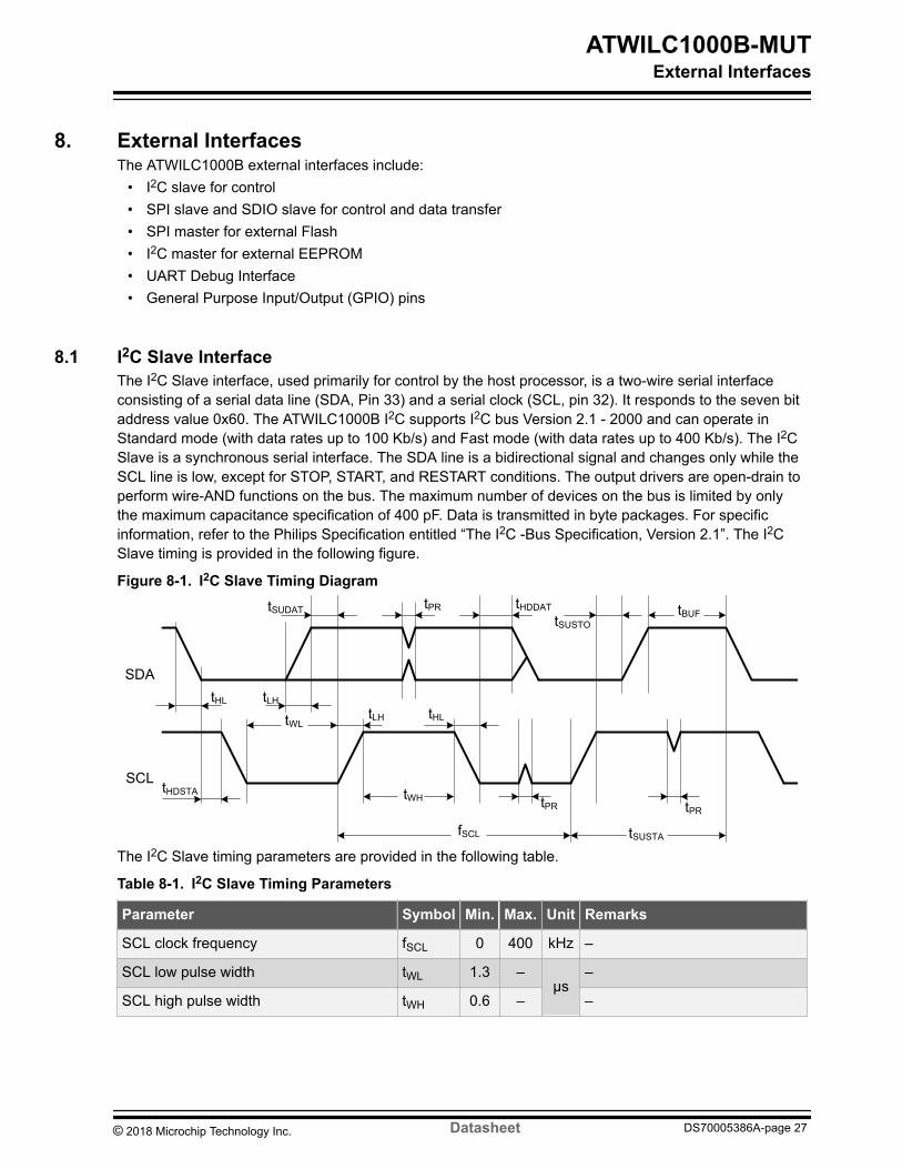
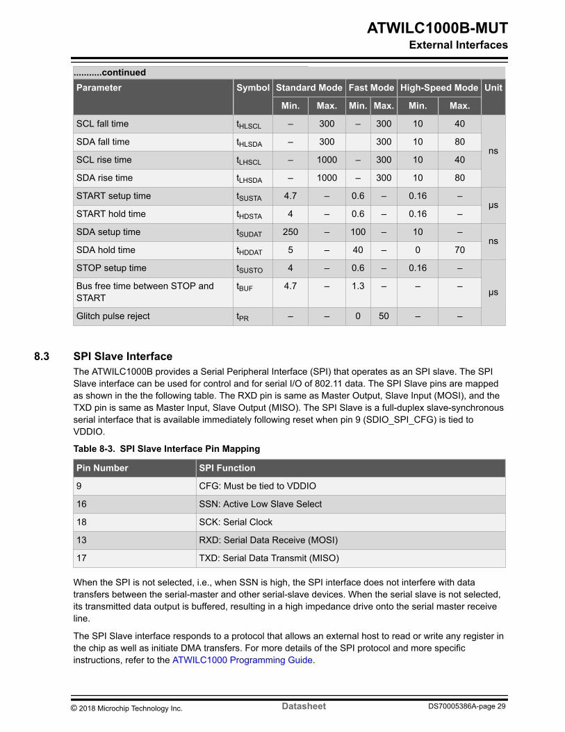
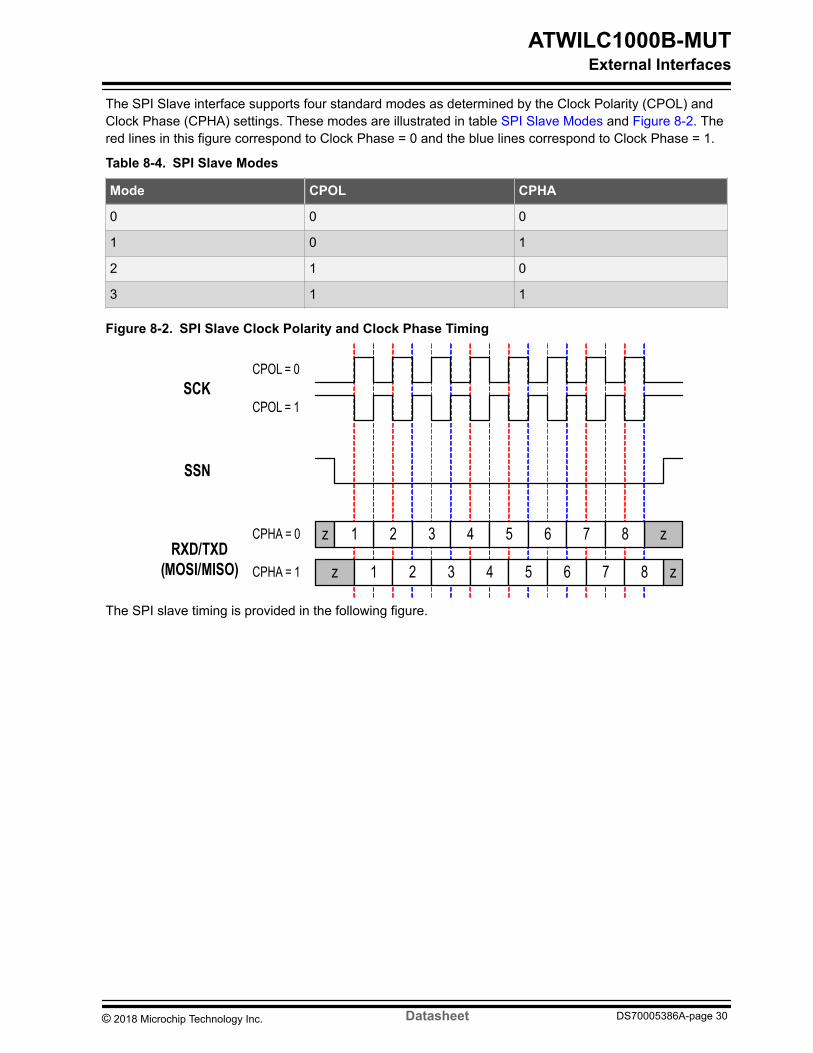
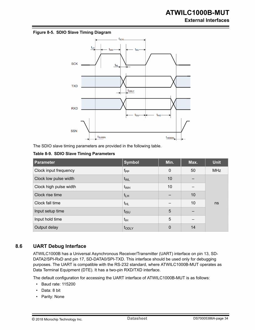
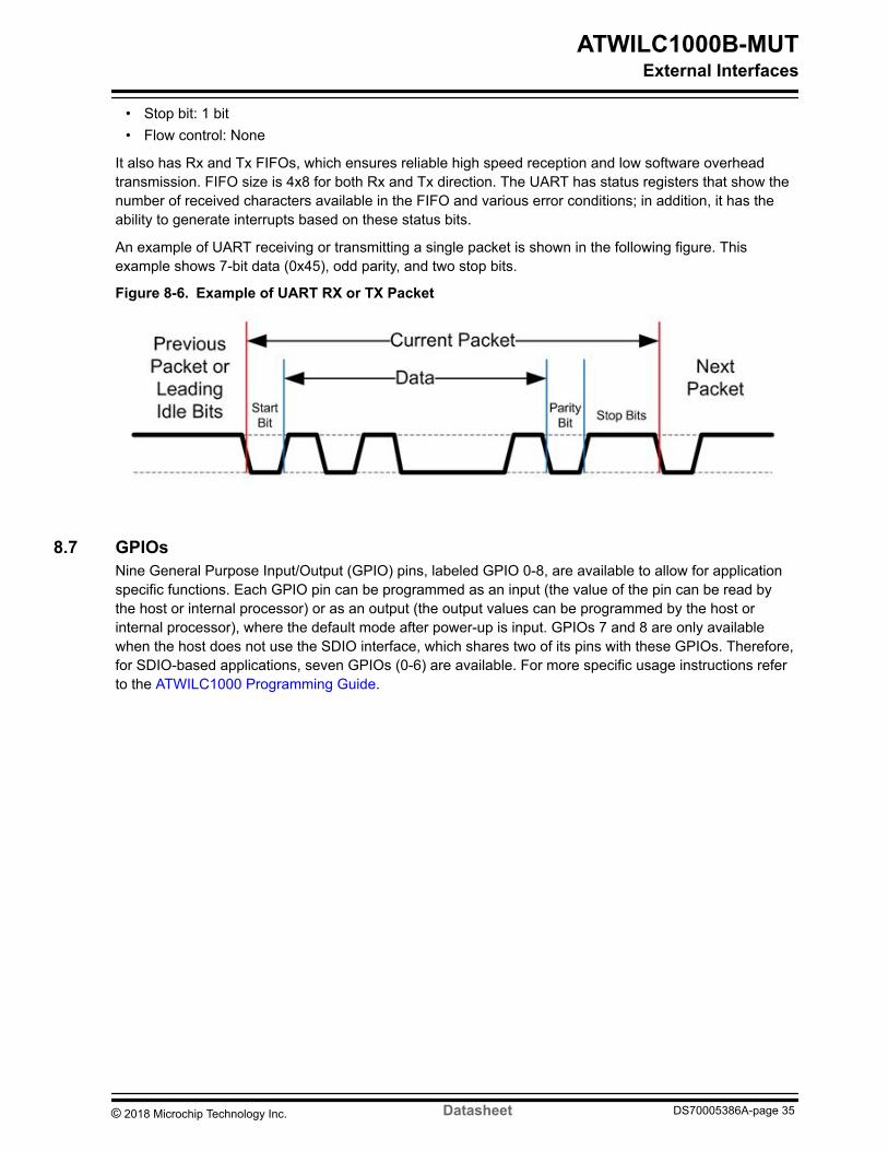
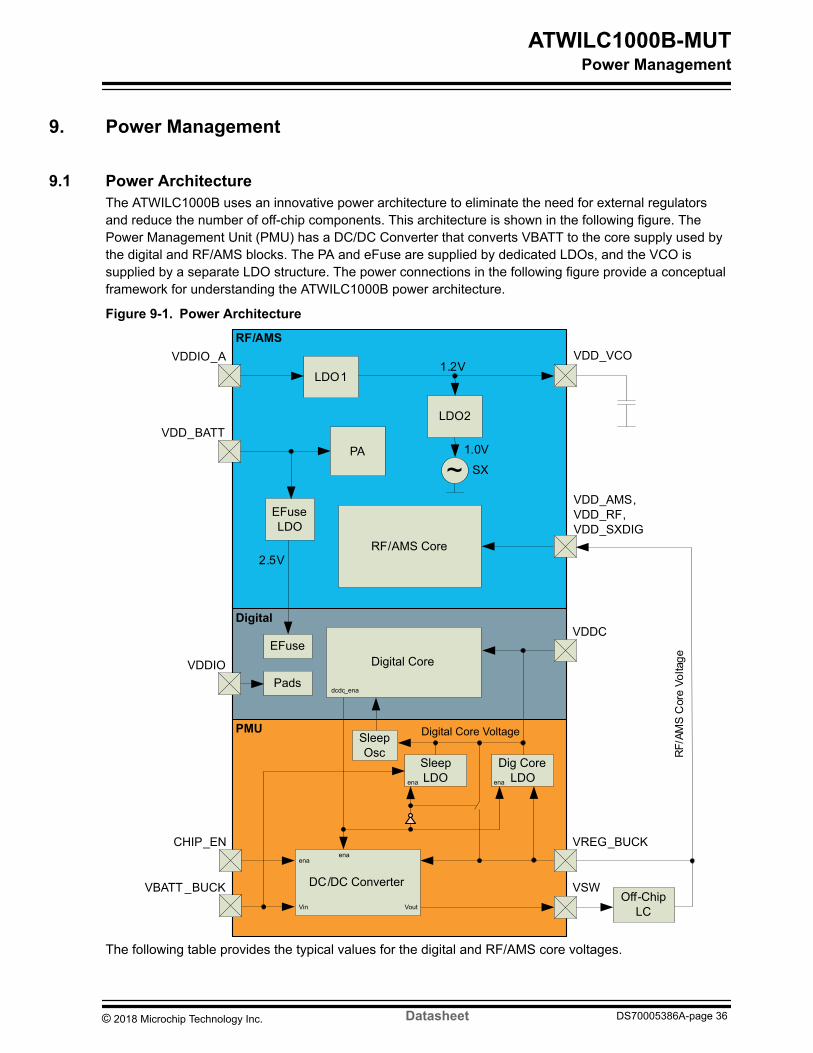
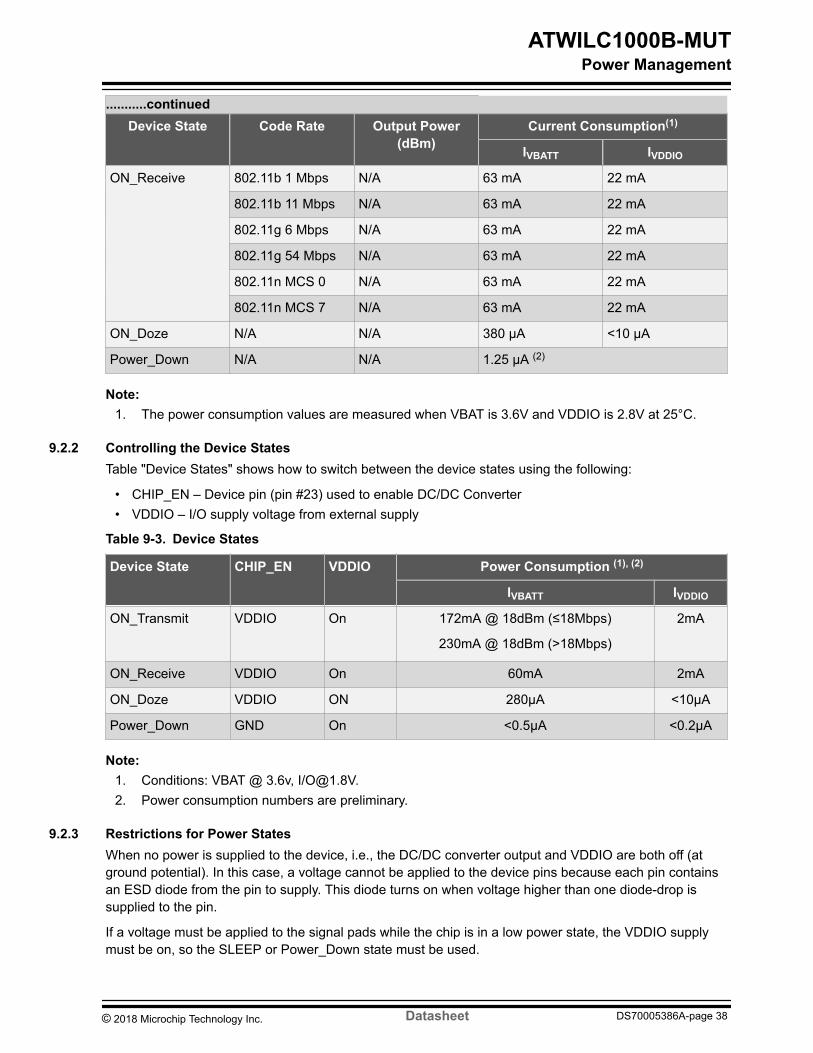
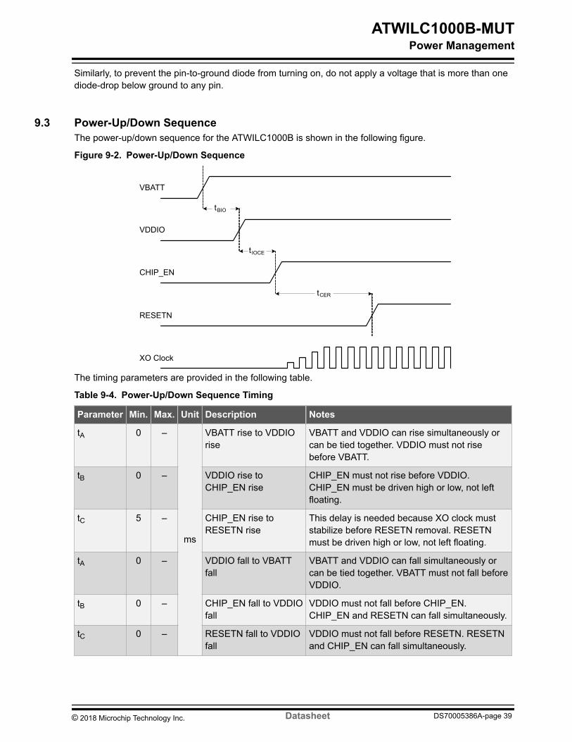
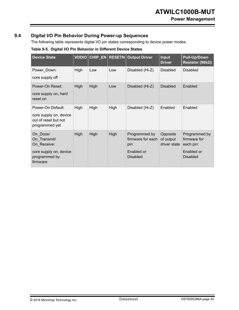
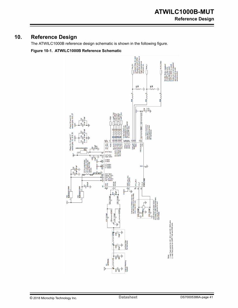
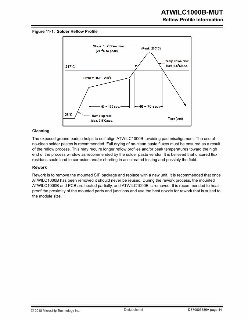