atom chips: a vision for neutral atom qip e.a. hinds imperial college, 11 july 2006 imperial college...
TRANSCRIPT


Atom chips:A vision for neutral atom QIP
E.A. Hinds
Imperial College, 11 July 2006
Imperial College London

• Videotape atom chip
• Atom guiding with microscopic wires
Outline
• Towards QIP
• MOT on a chip

Principle of the magnetic guide for atoms
Energy
B
1) Metallic atom chips
Energy
rr

Wire-guide apparatus at CCM

Loading the guide
Mirror MOT1 108 atoms 70 K
1.5 mm220 m
CompressedMagnetic trap
2 107 atoms 510 K
Magnetic trap2 107 atoms 80 K

1 mm 3 106 atoms
59 K
3 105 atoms
10 K
Evaporating to low temperature
2 104 atoms
0.3 KBEC
2 m 60 m
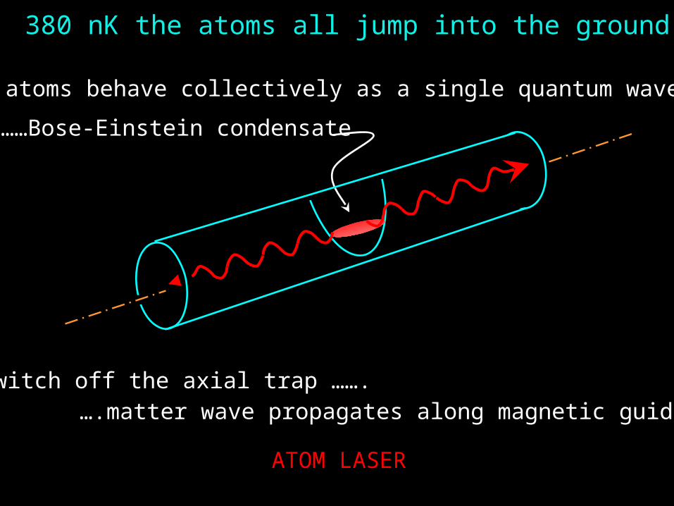
Below 380 nK the atoms all jump into the ground state
……Bose-Einstein condensate
The atoms behave collectively as a single quantum wave
ATOM LASER
Switch off the axial trap ……. ….matter wave propagates along magnetic guide

560 nK
380 nK350 nK
270 nK
Tc=380 nK
thermal cloud
BEC
Below 380nK the cloud Bose condenses
the atoms are now ready to be used….

23 mm
3.5 microns of gold
Au sputtered on a Si wafer, patterned by ion beam milling
67 m
atom interferometer on a chip
spectacular sensitivity too EM fieldso gravityo other feeble forces

metal slab
height
dissipation
resistivity of metal
fluctuating field outside
spin flips (and heating)
Johnson noiseHugely increases the spin flip rate
Henkel, Pötting and Wilkens Appl. Phys B 69,379 (1999)
11 s
Spin flip rate near a surface
skin depth
fast decay due topresence of surface modes

1
10
100
10 20 30 40 50 60 70 80 90 100
Height (um)
Lif
etim
e (s
)
1.8 MHz flip
560 kHz flip
TheoryPRA 70 013811 (2004)
S. Scheel
Spin flip lifetime above metal wire
Expt. PRL 91 080401 (2003)M. Jones

life
tim
e (s
)
skin depth (m)1
atom height = 50 m, say
10 100 10001
10
100
Atom/surface “impedance matching”
And what material has~ 50 m skin depth?
gold, aluminium, copper,…
skin depth ~ atom height
perfect conductor insulator
Ways to improve the traps near a surface:(i) Keep the metal thin
(ii) Use insulating surface
the subjectof part II

~200 G at surface
2) Videotape atom chip
Period ~100 m
Equivalent alternating currents
N S N S N
Alternating magnetization
N S N S N
Add a bias field to make an array of field zeros
where atoms are trapped

Loading a videotape microtrap NSNS
wire
videotape
still more bias-
+
collect atoms in mirror MOT
bias field
transfer to wire trap
more bias
off
keep bias
atoms now in microtrap
800nK320nK
<150nKmomentum distributions
Evaporate to make BEC
C. Sinclair et al. PRA (2005)

200 nK cloud, 45 m from surface
double image
SN
imaging light
6 kHz × 11 Hz
10 K cloud, 45 m from surface
~1000 atoms
Imaging the cloud
the BEC is ready for experiments…..and applications

e.g. oscillations viewed directly in the waveguide
Centre of mass oscillation at trap frequency f
Length oscillation at frequency √(12/5) f

pyramid MOT
Helicity flips on each reflection
3) Pyramid MOT on a chip

{100} Si wafer
SiO2 top layer
Si {111} pyramid
70.5o
This can prepare an integrated array
of many small clouds or single atoms(in progress)
integrated pyramid MOTs

What’s coming now?
2. entangling one atom with one photon
3. controlled entanglement of 2 atoms
1. making an atom qubit register
and QIP is in the works: e.g
integrated: atom interferometers clocks gyroscopes
.....etc.

1. making a quantum register
smooth trap
condensatephase coherent state
Take a condensate in a smooth trap
number state
Mott insulator
corrugated trap
Gradually corrugate the trap

laser lightoptical fibre
BECMott insulator
…………we are doing it on a videotape chip
The atom string can be a quantum information register

…………a quantum information register of atoms
each atom stores a bit of quantum information
…….the direction of the arrowspin-up represents 1
spin down represents 0 this atom represents0 and 1 both together
controlled collisions can do calculations
…….this leaves each atom entangled with its neighbour

90 m
concave mirrors etched in silicon
after coating with gold,we see focal spots under a microscope
2. entangling an atom with a photon

……… high finesse optical cavity
opti
cal fibre
0.9999 bragg stack
dielectric coated micro-mirror 0.9999
cavity length
reflection
finesse = 5 200
74 pm
390 nm
100 m
No atoms
One atom
• “strong coupling”g
g2/

this allows coherent atom-photon coupling
F = 2
F = 35S
5Pe.g. photon pistol
F = 2
F = 3
Coherent exchange of quantum information between atom and photon
optical interface to atom quantum memory
this idea leads to
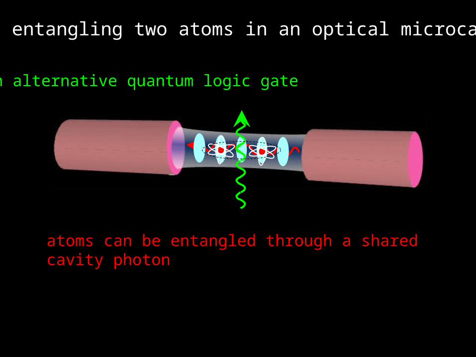
atoms can be entangled through a shared cavity photon
an alternative quantum logic gate
3. entangling two atoms in an optical microcavity
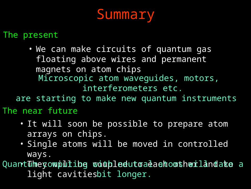
Summary
Microscopic atom waveguides, motors, interferometers etc.are starting to make new quantum instruments
• We can make circuits of quantum gas floating above wires and permanent magnets on atom chips
• It will soon be possible to prepare atom arrays on chips.
• Single atoms will be moved in controlled ways.• They will be coupled to each other and to light
cavities.Quantum computing with neutral atoms will take a bit longer.
The present
The near future

Many people work on these experiments
N S N S NQGATES
FASTNET
AtomChips
€ PPARC
Royal Society
EPSRC
£
Money
1D gas and Mott insulator Anne Curtis Isabel Llorente-Garcia Benoit Darquié
Wire chips & interferometry Stefan Eriksson Rob Sewell Daniel Sahagun-Sanchez Jos Dingian
Theory Stefan Scheel Duncan O’Dell
Michael Kraft Zak Moktadir Carsten GollaschFabrication
Single atom production and detectionGabriel Dutier Jonathan AshmoreMichael Trupke Jon Goldwin