arc fault protection - aktualności · 3.3.1. doc – device ... busbar bay, circuit-breaker bay...
TRANSCRIPT

Arc Fault Protection
User manual and technical documentation
Document version: 01i01 Update: 2016-04-01

Safety information
Dangerous voltages can occur on the connectors, even though the auxiliary voltage has been disconnected.
National and local electrical safety regulations must always be followed.
Exploration of damaged device can result in malfunction of protected object and result in threat to life and health.
Reliable and defect-free operation of the device needs appropriate transportation, handling, storage, installation and commissioning as well as correct operation and maintenance.
Uwagi
We reserve the right to modify the device.
Device is used for supervision and control in industrial facilities.
Remaining user documentation can be downloaded from energetyka.itr.org.pl.

IU_MAP_MANUAL_01i01_ENG 3 /20
1. Introduction................................................................................................................................. 4 1.1. Symbols ....................................................................................................................................... 4 2. General Information .................................................................................................................... 5 2.1. Designated use ............................................................................................................................ 5 2.2. Features ....................................................................................................................................... 6 2.3. Front panel .................................................................................................................................. 7 2.4. Signal diodes ................................................................................................................................ 7 3. Operation manual ....................................................................................................................... 8 3.1. Operation description ................................................................................................................. 8 3.2. Application examples .................................................................................................................. 9
3.2.1. Circuit-breaker bay ...................................................................................................................... 9 3.2.2. Arc protection with additional criteria ...................................................................................... 10 3.2.3. Cascade connection ................................................................................................................... 10
3.3. Diagnostic .................................................................................................................................. 11 3.3.1. DOC – Device Operation Check ................................................................................................. 11
4. Functional tests ......................................................................................................................... 12 4.1. EC directives and harmonized standards .................................................................................. 12 4.2. Electromagnetic compatibility .................................................................................................. 12
4.2.1. Immunity ................................................................................................................................... 12 4.3. Product safety requirements .................................................................................................... 14 4.4. Climatic environmental tests..................................................................................................... 14 4.5. Mechanical tests........................................................................................................................ 14 4.6. Degree of protection ................................................................................................................. 14 4.7. Installation requirements .......................................................................................................... 14 5. Technical parameters ................................................................................................................ 15 5.1. Input circuits .............................................................................................................................. 15
5.1.1. Arc detection optic inputs ......................................................................................................... 15 5.1.2. Binary inputs ............................................................................................................................. 15
5.2. Output circuits ........................................................................................................................... 15 5.2.1. Fiber outputs ............................................................................................................................. 15 5.2.2. Binary outputs ........................................................................................................................... 16
5.3. Power supply ............................................................................................................................. 16 5.4. Connectors ................................................................................................................................ 16 5.5. Mass and dimensions ................................................................................................................ 16 5.6. Time parameters ....................................................................................................................... 16 6. Description of connection sockets ............................................................................................ 17 7. Connection diagram .................................................................................................................. 17 8. Case sizes ................................................................................................................................... 18 9. Remarks of manufacturer ......................................................................................................... 19 9.1. Maintenance, inspections, repairs ............................................................................................ 19 9.2. Storage and transport ............................................................................................................... 19 9.3. Place of installation ................................................................................................................... 19 9.4. Disposal ..................................................................................................................................... 19 9.5. Guarantee.................................................................................................................................. 19 10. Order specification .................................................................................................................... 20 11. Contact ...................................................................................................................................... 20
4/20 IU_MAP_MANUAL_01i01_ENG
1. Introduction
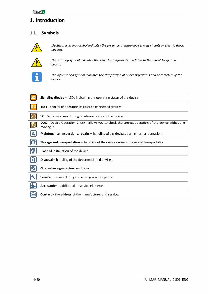
1.1. Symbols
Electrical warning symbol indicates the presence of hazardous energy circuits or electric shock hazards.
The warning symbol indicates the important information related to the threat to life and health.
The information symbol indicates the clarification of relevant features and parameters of the device.
Signaling diodes -4 LEDs indicating the operating status of the device.
TEST - control of operation of cascade connected devices
SC – Self check, monitoring of internal states of the device.
DOC – Device Operation Check - allows you to check the correct operation of the device without re-moving it.
Maintenance, inspections, repairs – handling of the devices during normal operation.
Storage and transportation – handling of the device during storage and transportation.
Place of installation of the device.
Disposal – handling of the decommisioned devices.
Guarantee – guarantee conditions.
Service – service during and after guarantee period.
Accessories – additional or service elements
Contact – the address of the manufacturer and service.

IU_MAP_MANUAL_01i01_ENG 5 /20
2. General Information
2.1. Designated use
MAP 6 is designed for use in switchgear as modular arc protection device. It is equipped with 6 inputs and 1 optical output. Accumulated input signal is transmitted to the optical output, this allows to build a selective security system. MAP 6, using binary inputs and outputs, can operate with the a bay control device, it also can operate autonomously. Device can directly open break-ers circuits in the bays, by the relay – semiconductor outputs (high rated power). States of opera-tion are indicated by diodes on the front panel.
Fig. 2.1 The view of MAP 6
MAP 6 device is equipped with a mechanism to facilitate the control of the device operation (DOC - Device Operation Check) and correctness of fiber optic connections between devices.
The multifunctional button starts testing of the device.
Regular 36-month guarantee period.

6/20 IU_MAP_MANUAL_01i01_ENG
2.2. Features
Operation in
all types of bays of low, medium and high voltage
Connector types
any breaker controlled by relay or relay – semiconductor outputs
Options of protections
unconditional
including the blocking from digital inputs
Diagnostic
SC - Selfcheck
memory: program and data
User interface
4 signal diodes
multifunction key
Other functions
Relay – semiconductor outputs (high rated power)
6 arc sensors support
installation on DIN TH 35 mm rail
other versions of supply voltages and nominal voltages of digital inputs
short time of signal propagation
cascade connection

IU_MAP_MANUAL_01i01_ENG 7 /20
2.3. Front panel
Fig. 2.3 Front panel
The front panel hosts:
1) number of input sockets of optical signals 1-6 2) power supply signaling diode 3) signaling diode TRIP of fiber output state 4) LOCK interlock signaling diode 5) signaling diode TEST of the device control of operation 6) key for active circuit breaker lock cancelling and power on / off Device Operation Check mechanism
(DOC)
2.4. Signal diodes
The diodes on the front panel are supposed to signal the most important states of device operation that re-sult, inter alia, from setting interlock (LOCK), switching on the TRIP optical output.
Tab 3.1.2 Meanings of predefined diodes
Diode Color Meaning
green Signals the proper level of power supply. Continuous light.
TRIP red Signals switching on the TRIP optical output.
LOCK orange Signals that the device is locked.
TEST blue Signals that the Device Operation Check (DOC) is activated.

8/20 IU_MAP_MANUAL_01i01_ENG
3. Operation manual
3.1. Operation description
Fig. 3.1.1 The simplified logic diagram of MAP 6
The main functional elements are mapped at a simplified logic diagram: 6 optical inputs and one optical out-put, 2 binary inputs and 2 binary outputs, TRIP and LOCK diodes. Optical sensors or outputs of another MAP6 devices can be connected to 6 optical inputs of device and all this signals will be summed. Logical summ is given to a fiber output and through memory area (it is not showed on pic. 3.1.1) to high rated power relay output (DO_1) and TRIP diode. Further signals from OI_1, OI_2 i OI_3 are summed using three-input system of auxiliary logical sum, and this sum is given to binary output DO_2. Signals of binary input block optical signals, and this state is signalling by LOCK diode. Protection tripping is signalling by continous light of TRIP diode and activating DO_1 relay output in 5s. This signal is repead every 1s, until the optical inputs are disactivated. If protection is activated by optical signal from IO_1, IO_2 or IO_3 input, also output DO_2 will be activated until multifunctional button will be pressed.
Reduction of supply voltage causes the reset of the device state and deactivation of the out-put relays. If the reduction of supply voltage occurred when TRIP signaling and relay output DO_2 were activated, then TRIP signaling and relay output will be restored after the reload of power supply.

IU_MAP_MANUAL_01i01_ENG 9 /20
3.2. Application examples
3.2.1. Circuit-breaker bay
Connection diagram of MAP 6 in switchgear bay equipped with circuit-breaker. 6 optical sensors are used, 2 in each bay: busbar bay, circuit-breaker bay and terminals bay. One of relay output can be connected directly to the breaker. Optional, second output can be connected to control bay device, for redundant protection and proper information about tripping by the bay control device. For example this configuration can be used in feeder bay, where opening of the circuit breaker cuts off an arc current. One of the optical inputs can be also used to connect the MAP 6 device placed in another bay, where opening of the circuit breaker does not cut off an arc current.
Fig. 3.2.1.1 Connection of MAP 6 in circuit-breaker bay
If you connect device as shown in Fig.3.2.1.2, you can adapt additional criteria of interlock for arc protection. In that case you should not connect MAP 6 device with bay control unit directly. Instead of this optical output of MAP 6 should be connected with optical input of bay control device and arc protection algorithm should be activated with additional criteria. This solution allows use much more optical sensors than using only of con-trol device.
Fig. 3.2.1.2 The insertion of additional criteria for arc protection

10/20 IU_MAP_MANUAL_01i01_ENG
3.2.2. Arc protection with additional criteria
If you use external relays measuring voltage U < connected to the digital inputs, you can improve the selectiv-ity of security and adapt additional criteria for arc protection. Connection diagram for this configuration is shown in Fig. 3.2.2.1. An alternative way of implement an additional criteria using the bay control device with arc protection algorithm is described in section 3.2.1.
Fig. 3.2.2.1 The insertion of additional criteria for arc protection
3.2.3. Cascade connection
MAP 6 can be used to combine signals from many optical sensors. This is useful when many signals from opti-cal sensors need be passed for superior circuit-breaker bay. By using the MAP 6 signals from one bay may be added together and pass for the next bay by a single fiber optic cable, where they are summed with the sig-nals from sensors installed in this bay and via MAP 6 are forwarded in the direction of the circuit breaker bay. This configuration is named the cascade connection. This is possible thanks to a very small time of propaga-tion of the optical signal from the optical input to the optical output, which does not exceed 12 µs. Addition even of a few propagation times can give a totally negligible time delay of the transmission of information about activation even a distant optical sensor. This is a competitive solution compared to systems based on connections using communication buses. MAP 6 may be pre-installed with optical sensors in the modular and prefabricated switchgears, which mini-mizes the time required to make connections during launch of switchgear. This solution reduces arc protec-tion wiring tracks to individual optical connections between adjacent bays. Example of application of the MAP 6 devices for arc protection the switchgear with four bays is shown in fig. 6. Four cascade connected devices collect signals from 20 optical sensors. The sum of this signals is putted to the bay control unit in the supply bay. Locally in each bay, if arc fault is detected by sensors connected to one of six inputs, signal from DO_1 output is brought to own breaker, which can be open immediately. In this case, the opening of the local circuit breaker effectively cuts off the arc supply current without opening the circuit breaker in the supply bay. Therefore, minimum delay of operation of the arc protection algorithm is necessary. This delay is entered naturally with the use of additional criteria U < , because voltage measure-ments is needed to done. The illustrated configuration of devices allows to realize progressive arc protection and causes a selectivity of this protection.

IU_MAP_MANUAL_01i01_ENG 11 /20
Fig. 3.2.3 MAP 6 usage in the four-pole switchgear
3.3. Diagnostic
3.3.1. DOC – Device Operation Check
MAP 6 device is equipped with a mechanism to facilitate the control of the device operation (DOC - Device Operation Check) and correctness of fiber optic connections.
Holding the button for 5 seconds starts the DOC mechanism. Switching to operation check mode is confirmed by a LED TEST. Square wave a 1 Hz frequency is generated at the outputs DO_1, DO_2 and OO_1 in control mode. The beat of this signal turns on and off the TRIP diode. The testing signal allows also to check fiber cascading connec-tions. Ending check mode occurs automatically after 15 seconds.

12/20 IU_MAP_MANUAL_01i01_ENG
4. Functional tests
4.1. EC directives and harmonized standards
EC Directive applies to: • Electromagnetic compatibility (EMC) 2004/108 / EC • Low-voltage electrical equipment (LVD) 2006/95 / EC
Tab. 4.1.1 Harmonized standards:
No. standards Title of the standard
PN-EN 60255-26:2014 Measuring relays and protection equipment –Part 26: Electromagnetic compatibility require-ments
PN-EN 60255-27:2014 Measuring relays and protection equipment –Part 27: Product safety requirements
PN-EN 60529:2003 Degrees of protection provided by enclosures (IP Code)
4.2. Electromagnetic compatibility
Tab. 4.2.1 Emission tests
Port Frequency range Limits Basic standard
Enclosure port 30 MHz – 230 MHz 40 dB(µV/m) quasi peak at 10 m
CISPR 11 230 MHz – 1000 MHz 47 dB(µV/m) quasi peak at 10 m
Auxiliary power supply port
0,15 MHz – 0,5 MHz 79 dB(µV) quasi peak
CISPR 22 66 dB(µV) average
0,5 MHz – 30 MHz 73 dB(µV) quasi peak
60 dB(µV) average
4.2.1. Immunity
Tab. 4.2.1.1 Input and output ports (including measuring ports)
Environmental phenom-ena
Test specification Description Basic standard Acceptance
criteria
Conducted disturbance induced by radio-frequency fields
Frequency sweep
PN-EN 61000-4-6 A
0,15-80 MHz Frequency range
10 V r.m.s.
80 %AM (1kHz) Amplitude Modulated
150 Ω Source impedance
Spot frequencies
27 MHz, 68 MHz Frequencies
10 V r.m.s.
80 %AM (1kHz) Amplitude Modulated
150 Ω Source impedance
100 % Duty cycle
Fast transient – Zone A
5/50 ns Tr/Th
PN-EN 61000-4-4 B 5 kHz Repetition frequency
4 kV Peak voltage
Slow damped oscillatory wave
1 MHz Voltage oscillation frequency
PN-EN 61000-4-12
B
75 ns Tr - Voltage rise time
400 Hz Repetition frequency
200 Ω Output impedance
1 kV Differential mode - peak voltage
2,5 kV Common mode - peak voltage
Surge - Zone B
1,2/50 (8/ 20) µs Voltage (current) rise time / time to half
value Tr /Th
PN-EN 61000-4-5 B 1 kV Line-to-line
2 kV Line-to-earth
2 Ω Source impedance
Power frequency - Zone B (concerns only binary
inputs)
Differential mode 100 V
Test voltage (r.m.s.) - Line-to-line PN-EN 61000-4-
16 A
Common mode 300 V
Test voltage (r.m.s.) - Line-to-earth

IU_MAP_MANUAL_01i01_ENG 13 /20
Tab. 4.2.1.2 Communication ports
Environmental phenom-ena
Test specification Description Basic standard Acceptance
criteria
Conducted disturbance induced by radio-frequency fields
Frequency sweep
PN-EN 61000-4-6 A
0,15-80 MHz Frequency range
10 V r.m.s.
80 %AM (1kHz) Amplitude Modulated
150 Ω Source impedance
Spot frequencies
27 MHz, 68 MHz Frequencies
10 V r.m.s.
80 %AM (1kHz) Amplitude Modulated
150 Ω Source impedance
100 % Duty cycle
Fast transient – Zone A
5/50 ns Tr/Th
PN-EN 61000-4-4 B 5 kHz Repetition frequency
2 kV Peak voltage
Slow damped oscillatory wave
1 MHz Voltage oscillation frequency
PN-EN 61000-4-12
B
75 ns Tr - Voltage rise time
400 Hz Repetition frequency
200 Ω Output impedance
0 kV Differential mode - peak voltage
1 kV Common mode - peak voltage
Surge - Zone A
1,2/50 (8/ 20) µs
Voltage (current) rise time / time to half value Tr /Th
PN-EN 61000-4-5 B 4 kV Line-to-earth
2 Ω Source impedance
Tab. 4.2.1.3 Auxiliary power supply port
Environmental pheno-mena
Test specification Description Basic standard Acceptance
criteria
Conducted disturbance induced by radio-frequency fields
Frequency sweep
PN-EN 61000-4-6 A
0,15-80 MHz Frequency range
10 V r.m.s.
80 %AM (1kHz) Amplitude Modulated
150 Ω Source impedance
Spot frequencies
27 MHz, 68 MHz Frequencies
10 V r.m.s.
80 %AM (1kHz) Amplitude Modulated
150 Ω Source impedance
100 % Duty cycle
Fast transient – Zone A
5/50 ns Tr/Th
PN-EN 61000-4-4 B 5 kHz Repetition frequency
4 kV Peak voltage
Slow damped oscillatory wave
1 MHz Voltage oscillation frequency
PN-EN 61000-4-12
B
75 ns Tr - Voltage rise time
400 Hz Repetition frequency
200 Ω Output impedance
1 kV Differential mode - peak voltage
2,5 kV Common mode - peak voltage
Surge - Zone A
1,2/50 (8/ 20) µs Voltage (current) rise time / time to half
value Tr /Th
PN-EN 61000-4-5 B 2 kV Line-to-line
4 kV Line-to-earth
2 Ω Source impedance
A.C. and D.C. voltage dips and voltage inter-
ruption 0% corresponds to the complete reduction of
supply voltage
0 % during ≤ 0,5 i 1 periods A.C. or ≤ 50 ms
D.C. PN-EN 61000-4-11
PN-EN 61000-4-29
A
C (for time
longer than specified)
40 % during ≤ 10 periods A. C. or ≤ 200 ms D.C.
70 % during ≤ 25 periods A. C. or ≤ 500 ms D.C.

14/20 IU_MAP_MANUAL_01i01_ENG
Tab. 4.2.1.4 Enclosure port
Environmental phenomena Test specification Basic standard Acceptance
criteria
Radiated radiofrequency electro-magnetic field
80-1000 MHz
IEC 61000-4-3 A 10 V / m (r.m.s.)
80% AM (1 kHz)
Electrostatic discharge
contact discharge 6 kV (charge voltage)
IEC 61000-4-2 B air discharge
8 kV (charge voltage)
Power frequency magnetic field
50 Hz or 60 Hz frequency
IEC 61000-4-8 A B
30 A (r.m.s.) / m - continuous
300 A (r.m.s.) / m - 1 to 3 s
4.3. Product safety requirements
Voltage test of solid insulation and insulation resistance measurements for auxiliary power supply, inputs, outputs, communication and measuring circuits:
Tab. 4.3.1 Product safety
Type of insulation test Value Basic standard
Dielectric voltage test 50 Hz or 60 Hz 2,2 kV/AC 1 minute or 3,1 kV/DC 1 minute
PN-EN 60255-27 Peak impulse voltage test 5 kV pulse 1,2/50 µs; 0,5 J
Insulation resistance >100 MOhm 500 VDC
4.4. Climatic environmental tests
Tab. 4.4.1 Climatic environmental test
Test Standard Description
Cold tests PN-EN 60068-2-1:2009 Minimum operational temperature -20˚C/16 hours Minimum storage temperature -55˚C/16 hours
Dry - heat tests PN-EN 60068-2-2:2009 Maximum operational temperature +55˚C/16 hours Maximum storage temperature +70˚C/16 hours
Damp - heat tests PN-EN 60068-2-78:2013-11 +40˚C; 95% rh /10 days
4.5. Mechanical tests
Tab. 4.5.1 Mechanical tests
Test Standard Class
Sinusoidal vibration PN-EN 60255-21-1:1999 Klasa 1 Single and multiple shocks and bumps PN-EN 60255-21-2:2000 Klasa 1
Seismic PN-EN 60255-21-3:1999/Ap1:2002P Klasa 0
4.6. Degree of protection
Tab. 4.6.1 Degree of protection
Test Description Standard Degree of protection
Degrees of protection provided by enclosures (IP Code)
Front panel side without plugged fiber slots
PN-EN 60529:2003
IP 20
Front panel side with plugged fiber slots or connected fibers
IP30
Connector side without connectors IP 20
Connector side with connectors plugged IP 30
4.7. Installation requirements
Tab. 4.7.1 Installation requirements
Definition Reguirements
Class equipment 2
Overvoltage category III
Pollution degree 2
Electrical environment B

IU_MAP_MANUAL_01i01_ENG 15 /20
5. Technical parameters
5.1. Input circuits
5.1.1. Arc detection optic inputs
Number of inputs 6
Connector type Avago
Maximum length of single sensor fiber connection 15 m
5.1.2. Binary inputs
Number of inputs 2
Input type voltage Maximum length of single cable connection < 3 m
Nominal voltage (4 versions) 24 V DC 110 V DC 220 V DC 230 V AC
Nominal voltage DC 24 V
Minimum excitation voltage DC 22 V Maximu de-excitation voltage DC 19 V
Current consumption before excitation < 11 mA
Current consumption after excitation ≤ 5 mA
Nominal voltage DC 110V
Minimum excitation voltage DC 90 V
Maximu de-excitation voltage DC 50 V
Current consumption before excitation < 4 mA
Current consumption after excitation ≤ 2 mA
Nominal voltage DC 220 V
Minimum excitation voltage DC 160 V
Maximu de-excitation voltage DC 150 V
Current consumption before excitation < 2 mA
Current consumption after excitation ≤ 1 mA
Nominal voltage AC 230 V
Minimum excitation voltage AC 125 V
Maximu de-excitation voltage AC 119 V
Current consumption before excitation < 2 mA Current consumption after excitation ≤ 1 mA
5.2. Output circuits
5.2.1. Fiber outputs
Number of outputs 1
Connector type Avago Maximum length of single sensor fiber connection 15 m

16/20 IU_MAP_MANUAL_01i01_ENG
5.2.2. Binary outputs
Number of outputs 2
including relay – semiconductor outputs (high rated power) 1
Relay – semiconductor outputs (high rated power)
Switching capability at resistance load DC 24 V, 8 A DC 250 V; 8 A; 2 kW, 1 s
AC 380 V; 8 A; 2 kVA
Switching rate at maximum contact load maks. 10/min
Contacts material AgCdO; AgCu/Au; 0,2mm
Relay outputs
Switching capability AT resistance load DC 24 V, 8 A DC 250 V; 0,1 A; 25 W
AC 380 V; 8 A; 2000 VA
Switching rate at maximum contact load maks. 10/min Contacts material AgCdO
5.3. Power supply
Nominal voltage 18-36 V DC
Power consumption <1,5 W
5.4. Connectors
Type screw connection
Connection wires 0,08..2,50mm2
5.5. Mass and dimensions
Mass < 0,2 kg
Dimensions (width, height, depth) 45/82/91 mm
5.6. Time parameters
The maximum delay from fiber input to fiber output 40 µs
The delay from digital input to digital output 20 ms
The delay from the fiber input to the digital output 10 ms The delay from the digital input to the fiber output 10 ms

IU_MAP_MANUAL_01i01_ENG 17 /20
6. Description of connection sockets
Tab.6.1 Connector X10
Terminal No. Description / Purpose
1 Fiber input OI_1
2 Fiber input OI_2
3 Fiber input OI_3
4 Fiber input OI_4
5 Fiber input OI_5
6 Fiber input OI_6
Tab.6.2 Connector X20
Terminal No. Description / Purpose
1 Optical output OO_1
Tab. 6.3 Connector X30
Terminal No. Description / Purpose
1 Digital input DI_1
2 Digital input DI_1
3 Digital input DI_2
4 Digital input DI_2
5 Relay output DO_2
6 Relay output DO_2
7 Relay – semiconductor output DO_1 (high rated power)
8 Relay – semiconductor output DO_1 (high rated power)
9 Power source
10 Power source
11 Protective grounding
12 Protective grounding
7. Connection diagram
X10 – Fiber inputs X20 – optical output X30 – Digital inputs, digital outputs and power source
X30
X10
X20
DO_
2
1
DO_
2DI_
_1DI
OO_1
_
3
OI
OI 1
_
4
_
_
6
_
OI
OI
5_
2
OI
OI
2
7
9
4
3
1
10
6
5
8
ARC
ARC
ARC
ARC
ARC
ARC
ARC
11
SUPPLY
12PE

18/20 IU_MAP_MANUAL_01i01_ENG
8. Case sizes
Fig. 8.1 Case sizes
IU_MAP_MANUAL_01i01_ENG 19 /20
9. Remarks of manufacturer
9.1. Maintenance, inspections, repairs
The manufacturer recommends that correctness of device operation is verified: a) each time - during commissioning, b) at least once a year - in mine face installations, c) at least once every 5 years in installations other than front face.
9.2. Storage and transport
Devices are packed in transport packages and secured against damage during transport and storage. De-vices should be stored in transport packages, indoors, in places free from vibrations and direct effects of weather conditions, dry, well ventilated, free from harmful vapors and gases. Ambient air temperature should be between –30°C and +70°C, and relative humidity should not exceed 80%.
9.3. Place of installation
MAP 6 device is designed for installation in power distribution stations on DIN TH 35 mm rail.
9.4. Disposal
Products are made mostly from recyclable materials, or materials that can be processed again or disposed of in environmentally sound manner. Decommissioned devices can be collected for recycling, provided that their condition is that of normal wear and tear. All components that are not recyclable shall be disposed of in environmentally sound manner.
9.5. Guarantee
Regular guarantee period is 36-month. Had the sale been preceded by execution of an Agreement be-tween the Buyer and the Seller, provisions of such Agreement shall apply. Guarantee covers remedying of defects, free of charge, provided that instructions specified in the Warranty Card are adhered to. Detailed guarantee conditions may be found at energetyka.itr.org.pl in the w „Sale Regulations”.
The guarantee period is counted from the date of sale.
The warranty is extended by a period of residence of the product in the repair.
Unauthorized tampering with the product will void the warranty.
Warranty does not cover damage resulting from improper use of the product.

20/20 IU_MAP_MANUAL_01i01_ENG
10. Order specification
A B Power source 24 V DC 1
Two-state input voltages 24 V DC 1
110 V DC 2
220 V DC 3
230 V AC 4
Order example:
MAP 6: A2.B4 – 24 V DC power source and 230 V AC two-state input voltages.
11. Contact
Tele- and Radio Research Institute ICT and Electronics Centre
03-450 Warsaw, ul. Ratuszowa 11
tel.: + 48 22 590 73 91 e-mail: [email protected] www: energetyka.itr.org.pl