applied physics reviews a critical literature review of
TRANSCRIPT
APPLIED PHYSICS REVIEWS
A critical literature review of focused electron beam induced depositionW. F. van Dorpa� and C. W. HagenFaculty of Applied Sciences, Delft University of Technology, Lorentzweg 1, 2628 CJ Delft, The Netherlands
�Received 6 March 2008; accepted 11 August 2008; published online 17 October 2008�
An extensive review is given of the results from literature on electron beam induced deposition.Electron beam induced deposition is a complex process, where many and often mutually dependentfactors are involved. The process has been studied by many over many years in many differentexperimental setups, so it is not surprising that there is a great variety of experimental results. Tocome to a better understanding of the process, it is important to see to which extent the experimentalresults are consistent with each other and with the existing model. All results from literature werecategorized by sorting the data according to the specific parameter that was varied �current density,acceleration voltage, scan patterns, etc.�. Each of these parameters can have an effect on the finaldeposit properties, such as the physical dimensions, the composition, the morphology, or theconductivity. For each parameter-property combination, the available data are discussed and �as faras possible� interpreted. By combining models for electron scattering in a solid, two different growthregimes, and electron beam induced heating, the majority of the experimental results were explainedqualitatively. This indicates that the physical processes are well understood, although quantitativelyspeaking the models can still be improved. The review makes clear that several major issues remain.One issue encountered when interpreting results from literature is the lack of data. Often, importantparameters �such as the local precursor pressure� are not reported, which can complicateinterpretation of the results. Another issue is the fact that the cross section for electron induceddissociation is unknown. In a number of cases, a correlation between the vertical growth rate and thesecondary electron yield was found, which suggests that the secondary electrons dominate thedissociation rather than the primary electrons. Conclusive evidence for this hypothesis has not beenfound. Finally, there is a limited understanding of the mechanism of electron induced precursordissociation. In many cases, the deposit composition is not directly dependent on the stoichiometriccomposition of the precursor and the electron induced decomposition paths can be very differentfrom those expected from calculations or thermal decomposition. The dissociation mechanism isone of the key factors determining the purity of the deposits and a better understanding of thisprocess will help develop electron beam induced deposition into a viable nanofabricationtechnique. © 2008 American Institute of Physics. �DOI: 10.1063/1.2977587�
TABLE OF CONTENTS
I. INTRODUCTION. . . . . . . . . . . . . . . . . . . . . . . . . . . . 2II. FOCUSED ELECTRON BEAM INDUCED
PROCESSES IN GENERAL. . . . . . . . . . . . . . . . . . . 3A. Substrate–precursor molecule interaction. . . . 3B. Electron-substrate interaction. . . . . . . . . . . . . . 4C. Electron–precursor molecule interaction. . . . . 4D. Interplay between factors. . . . . . . . . . . . . . . . . 5
III. THEORETICAL MODEL. . . . . . . . . . . . . . . . . . . . 6A. Basic model. . . . . . . . . . . . . . . . . . . . . . . . . . . 6B. Electron- and precursor-limited regimes. . . . . 6C. Temperature. . . . . . . . . . . . . . . . . . . . . . . . . . . 7
IV. BEAM PARAMETERS. . . . . . . . . . . . . . . . . . . . . . 8A. Current density. . . . . . . . . . . . . . . . . . . . . . . . . 8
1. Height. . . . . . . . . . . . . . . . . . . . . . . . . . . . . . 8
2. Width. . . . . . . . . . . . . . . . . . . . . . . . . . . . . . 103. Composition and morphology. . . . . . . . . . . 124. Density. . . . . . . . . . . . . . . . . . . . . . . . . . . . . 135. Conductivity. . . . . . . . . . . . . . . . . . . . . . . . . 14
B. Electron energy. . . . . . . . . . . . . . . . . . . . . . . . . 151. Height and width. . . . . . . . . . . . . . . . . . . . . 152. Composition and morphology. . . . . . . . . . . 173. Conductivity. . . . . . . . . . . . . . . . . . . . . . . . . 17
C. Conclusions. . . . . . . . . . . . . . . . . . . . . . . . . . . . 17V. SCAN PATTERN AND SCAN STRATEGY. . . . . . 18
A. Scan pattern. . . . . . . . . . . . . . . . . . . . . . . . . . . 181. Height and width. . . . . . . . . . . . . . . . . . . . . 182. Composition and morphology. . . . . . . . . . . 19
B. Scan strategy. . . . . . . . . . . . . . . . . . . . . . . . . . . 201. Height and width. . . . . . . . . . . . . . . . . . . . . 202. Conductivity. . . . . . . . . . . . . . . . . . . . . . . . . 21
C. Scan speed. . . . . . . . . . . . . . . . . . . . . . . . . . . . 21D. Writing direction. . . . . . . . . . . . . . . . . . . . . . . . 22
a�Electronic mail: [email protected].
JOURNAL OF APPLIED PHYSICS 104, 081301 �2008�
0021-8979/2008/104�8�/081301/42/$23.00 © 2008 American Institute of Physics104, 081301-1
Downloaded 15 Sep 2010 to 131.180.130.114. Redistribution subject to AIP license or copyright; see http://jap.aip.org/about/rights_and_permissions

1. Height. . . . . . . . . . . . . . . . . . . . . . . . . . . . . . 222. Composition and morphology. . . . . . . . . . . 23
E. Proximity effects. . . . . . . . . . . . . . . . . . . . . . . . 231. Deposit location. . . . . . . . . . . . . . . . . . . . . . 232. Composition and resistivity. . . . . . . . . . . . . 26
F. Conclusions. . . . . . . . . . . . . . . . . . . . . . . . . . . . 27VI. ADDITIONAL CIRCUMSTANCES. . . . . . . . . . . . 27
A. During experiments. . . . . . . . . . . . . . . . . . . . . 271. Substrate heating. . . . . . . . . . . . . . . . . . . . . 27
a. Height and width.. . . . . . . . . . . . . . . . . . 27b. Composition and morphology.. . . . . . . . 28c. Conductivity.. . . . . . . . . . . . . . . . . . . . . . 29
2. Tilting during deposition. . . . . . . . . . . . . . . 293. Biasing sample during deposition. . . . . . . . 29
B. Postdeposition treatment. . . . . . . . . . . . . . . . . . 291. Extra irradiation. . . . . . . . . . . . . . . . . . . . . . 292. Annealing. . . . . . . . . . . . . . . . . . . . . . . . . . . 30
a. Composition.. . . . . . . . . . . . . . . . . . . . . . 30b. Conductivity.. . . . . . . . . . . . . . . . . . . . . . 30
C. Conclusions. . . . . . . . . . . . . . . . . . . . . . . . . . . . 31VII. SUBSTRATE. . . . . . . . . . . . . . . . . . . . . . . . . . . . . . 31VIII. PRECURSOR. . . . . . . . . . . . . . . . . . . . . . . . . . . . . 33
A. Introduction. . . . . . . . . . . . . . . . . . . . . . . . . . . . 33B. Precursor gas only. . . . . . . . . . . . . . . . . . . . . . 33C. Reactive gases. . . . . . . . . . . . . . . . . . . . . . . . . . 35D. Precursor pressure. . . . . . . . . . . . . . . . . . . . . . . 36E. Conclusions. . . . . . . . . . . . . . . . . . . . . . . . . . . . 36
IX. CONCLUSIONS. . . . . . . . . . . . . . . . . . . . . . . . . . . . 37APPENDIX. . . . . . . . . . . . . . . . . . . . . . . . . . . . . . . . . . . 38
I. INTRODUCTION
Focused electron beam induced deposition �EBID� is alithography technique that allows the definition of patternson a substrate using electron beams �e-beams�. By scanning afocused e-beam over the sample in the presence of a precur-sor gas, the pattern is defined directly and �in principle� nopre- or postprocessing is required. It is mostly performed inelectron microscopes, so direct in situ inspection of the fab-ricated structure is very easy. Since e-beams can be focusedinto spots with diameters varying from micrometers down tothe subangstrom level, this direct-write process is suitable for
the micro- and nanometer regimes. Apart from deposition,the e-beam can also be used to induce other effects such aslocal etching or heating. Together, these processes are mem-bers of a family known as focused e-beam induced process-ing �FEBIP�.
FEBIP is a lithography technique that has been aroundfor many decades now, the first reports on the topic comingfrom Steward1 in 1934. He found contamination growth inhis electron optical system. While he considered the depositsas a “very insidious and prevalent source of errors,” some-thing that clearly needed to be avoided, Christy2 and Bakerand Morris3 were among the first to see a potentially usefulside of the technique and deposited conducting films. In re-cent years, FEBIP is a field of growing interest �see Fig. 1�.
Precursors used in FEBIP are contamination �carbonspecies from the residual gas in the electron optical system�,metal-organic precursors �for instance, W�CO�6 or trimethyl-platinum-cyclopentadienyl �Me3PtCp��, or inorganic precur-sors �for instance, WF6 or XeF2�. Typical examples of depos-its are shown in Fig. 2. One of the major advantages of beaminduced processing is that the pattern can be defined on flat�Fig. 2�a�� as well as topographical surfaces �Fig. 2�b��.4 Aslong as it is possible to focus the e-beam properly on thesample, deposition or etching can be performed. Another ad-vantage is that the fabrication of three-dimensional �3D�structures is possible. Regarding EBID, disadvantages are
FIG. 1. Number of publications as a function of the year of publication.Since the first mention of contamination growth in 1934, FEBIP gainedincreasing interest since the end of the 1980s.
FIG. 2. �Color online� Typical examples of beam induced deposits. �a� A topographical map of the world on a flat substrate. Note the presence of theHimalayas, the Rocky Mountains, and the Andes. �b� A tip grown on a scanning tunneling microscopy probe. From Ref. 4. Copyright © 1992 by Elsevier.Reprinted by permission of Elsevier. �c� High-resolution TEM image of a typical deposit showing a nanocomposite material �nanometer-sized metal crystalsin an a-C matrix�. From Ref. 5.
081301-2 W. F. van Dorp and C. W. Hagen J. Appl. Phys. 104, 081301 �2008�
Downloaded 15 Sep 2010 to 131.180.130.114. Redistribution subject to AIP license or copyright; see http://jap.aip.org/about/rights_and_permissions

the low growth rates compared to other lithography tech-niques such as e-beam lithography and the deposit composi-tion. The typical deposit created from metal-organic precur-sors consists of a nanocomposite material: metal crystals of afew nanometers in size embedded in a matrix of amorphouscarbon �a-C�. See also Fig. 2�c�.5 Such deposits containaround 10% metal and the other 90% is carbon and otherelements originally contained in the precursor molecule. In-organic precursors, especially the fluorine-based precursors,tend to yield deposits with higher metal concentrations.
In the course of time, many applications have been de-veloped. Examples are probes �functionalized tips for scan-ning probe microscopy or for local conductivitymeasurements�,6–14 conducting or nonconducting joiningtechnique,15–20 conducting wires,21–24 mask repair,25–27 elec-tron sources,28–30 micro-Hall and micro superconductingquantum interference devices,31,32 nanotweezers and grip-ping devices,33,34 nano-optic patterns or photoniccrystals,35,36 entire miniature electron optical systems,37
diodes,38 and seeds for nanotube growth.39
Despite its long history, detailed knowledge of the pro-cess is still very much dispersed. Not only “a plethora ofmaterials” has been studied, as Randolph et al.40 put it, butthe entire collection of publications on FEBIP can be de-scribed as a plethora of results. The fact that the depositionmember of the FEBIP family is known under many namesperfectly illustrates this unhelpful situation: EBID, e-beaminduced resist, e-beam induced metal formation, e-beam as-sisted deposition, e-beam induced selective etching anddeposition, e-beam induced chemical vapor deposition�CVD�, e-beam stimulated deposition, e-beam induced sur-face reaction, e-beam writing, environmental e-beam deposi-tion, e-beam assisted direct-write nanolithography, contami-nation lithography, additive lithography, or 3D depositionlithography.
Since FEBIP is a very complex phenomenon, it is im-portant to have an overview of all available useful resultsthat is as complete as possible. This is not the first review onFEBIP: reviews by Silvis-Cividjian and Hagen41 and Ran-dolph et al.42 appeared earlier and summarized publishedresults and achievements. It is felt that there is a need for amore critical review, in which it is determined to which ex-tent the available models for FEBIP are valid and complete.To do this, it is important to compare as many results aspossible and try to recognize the major trends. This overviewis an attempt at such a study. Out of the approximately 400articles that have appeared on FEBIP, we have selectednearly 200 articles. The results from these articles have beensorted and interpreted as far as possible using a model that ispresented. We do not claim to be fully complete, but we havetried to make this overview extensive. Since deposition is themost studied member of the FEBIP family, we restrict our-selves to EBID. For a good review on e-beam induced etch-ing, we refer the reader to Ref. 42.
This review serves three purposes: �1� To collect andsummarize relevant information from available literature, �2�to interpret this information and, where possible, compare toavailable �qualitative� models, and �3� to suggest strategiesfor further research into EBID.
The review is organized as follows. After giving a shortintroduction in Sec. II on the various parameters that areimportant for the process, we discuss the effect of each of theparameters that can be varied in the deposition process: thee-beam �Sec. III�, the scan pattern and the scan strategy �Sec.IV�, additional circumstances, such as heating of the sub-strate during or after deposition �Sec. V�, the substrate �Sec.VI�, and finally the precursor �Sec. VII�. We discuss the re-ported influence of these parameters on relevant properties ofthe deposition process and, if possible, we suggest a qualita-tive model. An explanation of the precursor names, the sym-bols, and the abbreviations that are used in this article arepresented in the Appendix. Conclusions from all describedresults and an outlook for further work are presented in Sec.IX.
II. FOCUSED ELECTRON BEAM INDUCEDPROCESSES IN GENERAL
The basic principle of FEBIP is quite simple. Gas mol-ecules �most commonly metal-organic molecules� are ad-sorbed on a substrate. Under the influence of the e-beam, theprecursor molecules are dissociated into volatile and non-volatile components. Depending on the type of precursor, thenonvolatile components adhere to the substrate and form adeposit �in the case of deposition� or react with the substrateand form volatile species �in the case of etching�. Hence, astructure is grown �Fig. 3�a�� or the substrate is etched �Fig.3�b��. This beam induced reaction occurs only locally at oraround the irradiated area. We now will go into more detailby describing the most important interactions playing a rolein FEBIP.
A. Substrate–precursor molecule interaction
The many different interactions complicate matters quiteseverely. To begin with, there are the interactions betweenthe substrate and precursor molecules, such as diffusion, ad-sorption, and desorption. Adsorption of the precursor mol-ecule may occur as chemisorption or physisorption depend-ing on the combination of precursor, substrate, andtemperature. The residence time � of the precursor moleculeon the substrate also can affect beam induced processes. Alonger � gives a higher probability of dissociation by theincoming or emitted electrons. Taking into account that themajority of the FEBIP experiments are done under non-UHVconditions, the precise condition of the vacuum and the sub-strate surface is generally unknown. Furthermore, as soon asthe deposition process starts in the case of deposition, the
FIG. 3. A schematic drawing of �a� beam induced deposition and �b� etch-ing. From Utke.
081301-3 W. F. van Dorp and C. W. Hagen J. Appl. Phys. 104, 081301 �2008�
Downloaded 15 Sep 2010 to 131.180.130.114. Redistribution subject to AIP license or copyright; see http://jap.aip.org/about/rights_and_permissions

interface of interest changes from the substrate surface to thedeposit surface. This transition stage is specifically importantfor the fabrication of high-resolution structures, where thegrowth is stopped in or soon after the nucleation stage of thedeposit.
B. Electron-substrate interaction
Then there are the interactions between the e-beam andsubstrate. At the start of the FEBIP experiment, a beam ofelectrons �primary electrons �PEs�� is focused onto a cleansubstrate. In a simplified picture, the PEs collide with thesolid and are deflected from their original trajectory. If aninelastic collision occurs, part of the initial energy can betransferred from the PE to other electrons in the solid. Theseelectrons will in turn interact with the solid and scatter. Thenewly generated electrons are called secondary electrons�SEs� if their energy upon leaving the substrate is smallerthan 50 eV and backscattered electrons �BSEs� if their en-ergy is larger than 50 eV.
The average length these electrons travel between twocollisions �the mean free path� is dependent on their energy.As a result of all these collisions, there is a �sort of onionshaped� volume of scattering events in the solid below theirradiated spot �Fig. 4�a��.43 The shape and the size of thisvolume depend on the PE energy and the substrate. From thisvolume, SEs and BSEs can escape from the substrate andenter into the vacuum. So on the substrate surface, aroundthe irradiated spot, there is an energy spectrum �Fig. 4�b��and a spatial distribution �Fig. 4�c��44 of emitted electrons.Monte Carlo simulations have been developed to model thisprocess.45–48 Precursor molecule dissociation can occur ev-ery time an electron crosses the interface between the sub-strate and vacuum.
Matters become more complicated by the fact that theshape and often the composition of the target change duringthe FEBIP experiment. In the case of beam induced deposi-tion, for instance, a pillar can grow and the electron scatter-ing volume will become more confined to the pillar as itbecomes longer. Electrons �for instance, forward scatteredelectrons �FSEs�� can also cross the target-vacuum interfaceseveral times �Fig. 4�d��. As a result of the electron scatter-ing, there is a constant energy transfer from the PEs to thesubstrate and/or the growing structure, which may lead toe-beam induced heating. Furthermore, if the target is electri-cally nonconducting, a difference between the fluxes of in-bound PEs and outbound SEs and BSEs can lead to chargingof the sample. Finally, when the PE energy is around 50 keVor larger, physical sputtering of the target material by thehigh-energy PEs can occur.49 This is especially relevant forFEBIP experiments in �scanning� transmission electron mi-croscopes ��S�TEMs�, where the acceleration voltage is usu-ally 200–300 keV.
C. Electron–precursor molecule interaction
Finally, there is the interaction between the electrons andthe precursor molecules. Dissociation is the most importantone for this review, but e-beam stimulated desorption alsocan occur. The probability that an electron induces the scis-sion of a bond in a precursor molecule depends on the elec-tron energy and is generally expressed as a cross section ��E��cm2�. The larger the cross section, the larger the probabilitythat a bond in the molecule is broken. The cross section fordissociation of adsorbed molecules is a difficult issue since itdepends on many parameters. It depends, for instance, on theenergy of the bonds within the molecule and is strongly in-fluenced by the environment, the available reaction paths for
FIG. 4. �Color online� �a� A schematicof the electron scattering volume in aflat substrate �from Ref. 43�. �b� Atypical energy spectrum of electronsemitted from the substrate �from Ref.43�. The PE energy is equal to eU. �c�Top view of �simulated� SE emissionsites on a flat substrate, showing thespatial distribution. From Ref. 44. �d�In the case of a growing 3D deposit,electrons can cross the target-vacuuminterface in many different ways. Fortips longer than the BSE range, theelectron scattering volume will bemore confined to the tip. Copyright© 1998 by Springer-Verlag. Reprintedwith permission by Springer-Verlag.
081301-4 W. F. van Dorp and C. W. Hagen J. Appl. Phys. 104, 081301 �2008�
Downloaded 15 Sep 2010 to 131.180.130.114. Redistribution subject to AIP license or copyright; see http://jap.aip.org/about/rights_and_permissions

the dissociation event, or even the specific geometry inwhich the molecule is adsorbed. Studies on the interactionbetween adsorbed molecules and low-energy electrons showthat dissociative electron attachment �DEA� and dipolar dis-sociation �DD� are important processes.50 Energies as low asa few eV can be sufficient to induce the scission of bonds inprecursor molecules, such as for hydrocarbons present on acontaminated sample51 and hexafluoro-acetylacetonate cop-per vinyl-trimethyl-silane �hfac-Cu-VTMS�.52 George andBeauchamp53 used broad area UV irradiation to induce pre-cursor decomposition and found that the yield was primarilydependent on the photoelectron yield of the substrate. Therewas no deposition when the photon energy was below thephotoelectron emission threshold. In Fig. 5�a�, three crosssections for low-energy electron induced dissociation areplotted for Fe�CO�5. Rowntree reported �AB and �BC, crosssections for a two-step dissociation, from the originalFe�CO�5 molecule �A� into an intermediate species �B� andfrom B into the final material that remains after prolongedirradiation �C�.54 Henderson et al.55 measured �total, the totalcross section for the dissociation of a monolayer of adsorbedFe�CO�5.
These studies clearly indicate that low-energy electrons�i.e., SEs� are relevant for the deposition process. However,they do not exclude the possibility that electrons with ahigher energy can also contribute to the growth. This can be,for instance, by dissociative ionization �DI�, which typicallyhas a cross section �measured for molecules in the gas phase�with a peak at around 100 eV and decreases with increasingelectron energy.59
The mentioned dissociation mechanisms �DEA, DD, andDI� have cross sections that have their maximum well below1 keV. One may be tempted to conclude from this that thedeposit growth is determined by electrons with energies�1 keV, but that could be premature. In the typical FEBIPexperiment, the current density of �1 keV electrons in thearea directly under the PE beam is very high compared to thecurrent density of low-energy electrons. That means that, al-
though the absolute cross sections for high-energy electronsmay be small, the absolute number may be high enough tomake their contribution to deposit growth significant �seeFig. 5�b��. Definite conclusions cannot be drawn since thereis little information on the balance between the contributionsof low- and high-energy electrons to the dissociation of ad-sorbed molecules.
As a result, there is no consensus yet on this particulartopic in the field of FEBIP research. The lack of informationbecomes most evident in the different Monte Carlo simula-tions that have been developed to model the deposit growth.In these simulations, a dissociation cross section has to beassumed. Silvis-Cividjian et al.56 concentrated on the effectof electrons with energies �1 keV, while Fowlkes et al.57
took a more even balance between low- and high-energyelectrons. Mitsuishi et al.58 on the other hand used a crosssection where the low-energy cutoff was set at 35.5 eV. Thethree cross sections are plotted in Fig. 5�a�.
Apart from influencing the growth rates, it is also con-ceivable that the different dissociation processes �DEA, DD,and DI� influence the composition of the deposit. It is pos-sible that the dissociation mechanism determines which frag-ment of the molecule desorbs after electron impact. Ideally,all carrier groups desorb and only the target material �forinstance, Fe in the case of Fe�CO�5� remains in the deposit.In any case, to advance the understanding and modeling ofFEBIP, the progress of the study of dissociation processessuch as DEA, DD, and DI is very important.
D. Interplay between factors
Looking at the three types of interactions discussed inSecs. II A and II C, it appears that there are many factorsinvolved in the deposition process. One can think of the elec-tron flux, the energy spectrum of the electrons that cross thesubstrate-vacuum interface, the spatial distribution of elec-tron scattering in the irradiated target, the cross section of theprecursor as a function of electron energy, the precursor ad-sorption behavior �physisorption, chemisorption�, the precur-
FIG. 5. �a� Measured and estimated cross sections for the dissociation of precursors often used in EBID. Cross sections for Fe�CO�5 are reported by Rowntree��AB and �BC� �Ref. 54� and Henderson et al. ��total� �Ref. 55�. In Monte Carlo simulations, cross section for C2H5 �Silvis-Cividjian et al., Ref. 56�, WF6
�Fowlkes et al., Ref. 57�, and W�CO�6 �Mitsuishi et al., Ref. 58� were used. �b� The simulated energy distribution of SEs and BSEs emitted from a Gesubstrate and the estimated cross section for the dissociation of WF6 as a function of electron energy. All distributions are normalized. From Ref. 58.
081301-5 W. F. van Dorp and C. W. Hagen J. Appl. Phys. 104, 081301 �2008�
Downloaded 15 Sep 2010 to 131.180.130.114. Redistribution subject to AIP license or copyright; see http://jap.aip.org/about/rights_and_permissions
sor residence time on the substrate, the precursor diffusion�electron stimulated� desorption, the e-beam induced heating,the gas flux, the orientation of the precursor source withrespect to the deposition location, the deposit or surface ge-ometry, the chemical reaction paths that are available, thebackground gas pressure and composition, or the thermal andelectrical conductances of the substrate and deposit. All ofthese factors act simultaneously and many of them only lo-cally in or around the irradiated area. The factors are notindependent of each other and, since the shape of the irradi-ated target evolves during the process, the dependence is notconstant. Furthermore, as if matters were not complexenough, most of the FEBIP experiments are performed undernon-UHV conditions, so often quite a number of factors dur-ing the experiment are unknown and/or uncontrolled. Theinterplay between all these factors can lead to an immensevariety of possible phenomena, of which perhaps only asmall part has yet been observed and is reported in this over-view.
III. THEORETICAL MODEL
A. Basic model
Before discussing experimental results, it is helpful tosee what we can expect based on the description of the pro-cess given in Sec. II. Many parameters were mentioned andnot all of these parameters can be put into a theoreticalmodel straight away. So to study the effect of some of theparameters, we start with a rather simple model similar tothat suggested by Scheuer et al.60 Starting with the precursormolecule coverage N �cm−2�, it will depend on the number ofmolecules that adsorb from the gas phase, the number ofmolecules that are decomposed by the e-beam, and the num-ber of molecules that desorb to the gas phase. This gives
dN
dt= gF�1 −
N
N0� − ��E�NJ −
N
�, �1�
with g the sticking factor, F �cm−2 s−1� the gas flux arrivingat the substrate, N0 �cm−2� the available adsorption site den-sity in a monolayer, J �electrons s−1 cm−2� the current den-sity, and � �s� the residence time of precursor molecules onthe surface. Usually, two simplifications are made. As ex-plained in Sec. II C, the cross section for dissociation, ��E�, isdependent on the electron energy. Since ��E� is unknown, �
�the integral value of ��E�� is used. Furthermore, in realityJ=JPE+JBSE+JSE, where JPE, JBSE, and JSE are the PE, BSE,and SE current densities, respectively. Since JBSE and JSE areusually not measured during experiments, it is assumed thatJ=JPE. Steady-state situation for the coverage N is reachedwhen dN /dt=0, which means
N = N0�gF
N0
gF
N0+ �J +
1
�� . �2�
If the growth rate R �cm s−1� is defined as
R = VmoleculeN�J , �3�
with Vmolecule �cm3� the volume of a deposited molecule, thecombination of Eqs. �2� and �3� gives
R = VmoleculeN0
�gF
N0��J
�gF
N0+ �J +
1
�� . �4�
B. Electron- and precursor-limited regimes
We will now look at two simplified cases that give usinsight into the deposition process. For simplicity, desorptionis ignored. Two distinguishing regimes can be defined:gF /N0��J and gF /N0��J. This reduces Eq. �4� to
gF
N0� �J, R = VmoleculeN0�J , �5�
gF
N0� �J, R = VmoleculegF . �6�
In the first regime, the growth is limited by the current den-sity and has become independent of the gas flux. This isdefined as the electron-limited �e.l.� regime. In the secondregime, the growth is limited by the number of moleculesarriving at the irradiated area and has become independent ofthe current density. This is defined as the precursor-limited�p.l.� regime. The effect of the two different regimes can belarge. For a constant area, a change in J is a change in thetime scale at which a specific number of electrons is sup-plied. This not only affects R but it can also affect otherdeposit properties. The ratio of electrons per deposited mol-ecule can change dramatically, which can give different de-grees of fragmentation.
Practical reasons for measuring the growth rate are, forinstance, to determine the rate of contamination growth in anelectron optical system, to find suitable growth conditions forthe fabrication of applications, or to study fundamental as-pects of the deposition process. We will see in Sec. IV thatmeasurements of the growth rate are presented in differentways in literature. Different units are used: some authorsreported Vdeposit �nm3�, some reported R �nm s−1�, and somereported the deposit height h �nm�. This is measured as afunction of J, beam current I �electrons s−1�, or the accumu-lated charge Q �C�. The relations are
Vdeposit = RtdwellAdeposit, �7�
h = Rtdwell, �8�
I = JAbeam, �9�
Q = Itdwell, �10�
with tdwell �s� the dwell time, Adeposit �cm2� the area of thedeposit, and Abeam �cm2� the area of the e-beam.
The various ways results are presented complicate thecomparison of results from the different sources. Anothercomplicating matter is that in �nearly� every electron opticalsystem, the beam diameter �dbeam� changes when I is
081301-6 W. F. van Dorp and C. W. Hagen J. Appl. Phys. 104, 081301 �2008�
Downloaded 15 Sep 2010 to 131.180.130.114. Redistribution subject to AIP license or copyright; see http://jap.aip.org/about/rights_and_permissions

changed. A change in dbeam will affect R �if deposition isdone in spot mode� because ddeposit will change accordingly.If Vdeposit is kept constant and ddeposit decreases, R becomeshigher. In many cases, dbeam or ddeposit are not measured orreported, in which case it is not clear how R or h should beinterpreted precisely. To avoid this complication for caseswhere only I is reported, we restrict ourselves to measure-ments of Vdeposit as a function of I. This complication is ab-sent for measurements where h was reported as a function ofJ because both parameters are expressed per area, see Eqs.�7�–�9�.
It was mentioned in Sec. II that the growth regimes canbe of significant influence. It is interesting to see how thetwo regimes can be recognized in the various representationswe have just discussed. The e.l. and p.l. regimes are indi-cated in Fig. 6. At low current densities, gF /N0��J and h islinearly dependent on J �according to Eq. �5��. At high cur-rent densities, gF /N0��J and h becomes independent of J�according to Eq. �6��. The same behavior is observed whenVdeposit is used instead of h except for the scaling with ddeposit.
Alternatively, h can be plotted as a function of Q, Ac-cording to Eq. �9�, there are two ways to do this: either varyJ �or I� and keep tdwell constant or vary tdwell and keep Jconstant. Both cases are shown in Fig. 7. The first case,where J is varied �Fig. 7�a��, is the same situation as in Fig.6. In the second case, where tdwell is varied, the e.l. and p.l.regimes are characterized merely by a different slope �Fig.7�b��.
Yet another representation of the deposit growth behav-ior is a plot of h as a function of tdwell for a constant I �seeFig. 7�c��. These are basically the same data as shown in Fig.7�b�, and both plots can be made for the same experiment.The difference is that in Fig. 7�c� the time scale is madevisible. Similarly, the growth regime cannot be easily distin-guished in the plot of h versus Q since the regimes are againcharacterized merely by a different slope.
The measurements of the deposited amount of materialas a function of the growth conditions allow for a determi-nation of the growth efficiency. This can be defined as theincrease in h per PE �nm/electron�. From the definition of thetwo regimes, it becomes clear that the growth efficiency ishighest in the e.l. regime and lowest in the p.l. regime.
C. Temperature
The simplifications made in Sec. II are not allowed whenthe effect of desorption cannot be ignored. This is, for in-stance, the case when the temperature is varied to study theeffect on the growth rate, composition, or conductivity orwhen the temperature is not constant during the depositionprocess. In these cases, the temperature will influence theresidence time of molecules on the substrate. The relationbetween � and temperature can be expressed by
� =1
�exp�Edes
kT� , �11�
where � is the vibrational frequency of an adsorbed molecule�s−1�, Edes is the desorption energy �J�, k is the Boltzmannconstant �m2 kg s−2 K−1�, and T is the temperature �K�.Qualitatively speaking, Eq. �11� shows that as the tempera-ture increases, � will decrease. In Eq. �4�, a decrease in � willlead to a decrease in R. Therefore, as the temperature in-creases, the growth rate will decrease.
How the temperature affects the growth rate quantita-tively cannot be established that easily. A situation where thegrowth is either e.l. or p.l. limited can still be obtained, butthe conditions under which this occurs are less straightfor-ward to estimate.
FIG. 6. Schematic of the deposit height h as a function of J.
FIG. 7. Schematic of the deposit height h as a function of Q. The e.l. andp.l. regimes are indicated. �a� Behavior where J �or I� is varied and tdwell iskept constant. �b� Behavior where tdwell is varied and J �or I� is kept con-stant. �c� Same as �b� but now as a function of tdwell.
081301-7 W. F. van Dorp and C. W. Hagen J. Appl. Phys. 104, 081301 �2008�
Downloaded 15 Sep 2010 to 131.180.130.114. Redistribution subject to AIP license or copyright; see http://jap.aip.org/about/rights_and_permissions
IV. BEAM PARAMETERS
A. Current density
1. Height
Now that we have a �simple� growth model and knowhow to interpret it, we can discuss results from literature. InFigs. 8�a�–8�c� h as a function of J is plotted for five differ-ent experiments. The data are shown in three different graphsto present the different orders of magnitude and yet still uselinear scales. Linear behavior is found for deposition withPt�PF3�4 and Os3�CO�12, while for Ru3�CO�12, diffusionpump oil, and SiH2Cl2 the h saturates with increasing J.Based on the model discussed in Sec. III, this means that ane.l. regime was found for Pt�PF3�4 and Os3�CO�12, and a p.l.regime was found for Ru3�CO�12, diffusion pump oil, and
SiH2Cl2. The different results can be explained quantitativelyto a �relatively� large extent. For instance, based on the re-sults for Ru3�CO�12 where growth was p.l., one would expectthat growth was p.l. for Pt�PF3�4 too because J was largest inthe latter case. However, the opposite is true. This can beexplained by differences in ��E� and F. The amount of elec-trons needed for the dissociation of one Pt�PF3�4 molecule isestimated62 at 1.8�103, and for Ru3�CO�12 this was about280.60 The gas flux in the experiment with Pt�PF3�4 waslarger than in the experiment with Ru3�CO�12 �1�1016 ver-sus 3�1014 molecules cm−2 s−1�. These two differences ex-plain the two growth regimes. For the experiment with dif-fusion pump oil, the p.l. regime can be explained by thelimited F �about 5�1011 molecules cm−2 s−1�. In the experi-ment with SiH2Cl2 a significantly larger precursor flux wasused �in the order of 1016 molecules cm−2 s−1�,61 but becauseJ was a factor of 105 times larger than for the other experi-ments, growth was still p.l.. The only case for which a quan-titative explanation is difficult to give is Os3�CO�12. ForOs3�CO�12, h was higher �see Fig. 8�c�� and F was lowerthan for Ru3�CO�12,
60 but the growth was still in the e.l.regime. The higher h indicates that either ��E� or N waslarger. If F was lower, N can only be larger if the stickingcoefficient was higher. One would expect that both a higher��E� and a higher sticking coefficient would lead to a p.l.regime, but the linear dependency on current density indi-cates that the growth is e.l.. An explanation was not given bythe authors.
Measurements of Vdeposit as a function of I are shown inFigs. 9�a� and 9�b�. For all data points tdwell was 120 s. Forthe experiment with tetra-ethoxy-silane35 �TEOS� ��� twothings can be noticed for the change from 20 to 100 pA: �1�Vdeposit is larger at 100 pA than that at 20 pA and �2� Vdeposit
saturates. This indicates that the growth regime changes frombeing e.l. to being p.l. between 20 and 100 pA. The samebehavior, except now in extreme form, is observed for thedeposition with dimethyl acetylacetonate gold�Me2-Au-acac� ���.15 The increase in Vdeposit is roughly lin-ear for beam currents of about 2–200 pA, which indicates thee.l. regime. When a significantly larger amount of electrons�beam current of 6 nA instead of 200 pA� is supplied in thesame time span, Vdeposit saturates. This indicates the p.l. re-gime.
An entirely different behavior is observed for the experi-ment with contamination ���.9 For low beam currents �be-tween 3 and 30 pA� Vdeposit increases roughly linearly withincreasing I. However, when I is increased above 30 pA �upto 200 pA�, Vdeposit decreases. A similar behavior was foundfor contamination growth for beam currents �25 pA byMiura et al.38 �not shown because the dwell times used werenot reported�. A decrease in Vdeposit does not mean that ma-terial was removed from a deposit but that less material wasdeposited in the same dwell time. F was constant during theentire experiment, so the number of molecules arriving at theirradiated area was also constant. The decrease in Vdeposit
could be the result of a decrease in Vmolecule at higher beamcurrents. Extrapolating R from low I �i.e., from the e.l. re-gime� to 200 pA, this would be a decrease in Vmolecule in theorder of 103. Such a strong decrease is not very likely. There-
FIG. 8. Tip height as a function of the current density. Data are plotted inthree graphs to present the different orders of magnitude and yet still uselinear scales: ��� diffusion oil pump �Christy, Ref. 2�, ��� SiH2Cl2 �Ichiashiand Matsui, Ref. 61�, ��� Os3�CO�12 �Scheuer et al., Ref. 60�, ���Ru3�CO�12 �Scheuer et al., Ref. 60�, and �gray triangle� Pt�PF3�4 �Wang etal., Ref. 62�.
081301-8 W. F. van Dorp and C. W. Hagen J. Appl. Phys. 104, 081301 �2008�
Downloaded 15 Sep 2010 to 131.180.130.114. Redistribution subject to AIP license or copyright; see http://jap.aip.org/about/rights_and_permissions

fore, this decrease cannot be explained anymore with thesimplified model we used to describe the e.l. and p.l. regimesand we must turn to the more complicated model that in-cludes the residence time �. As mentioned in Sec. III C, adecrease in � will lead to a decrease in R and therefore inVdeposit
If all other conditions are kept constant during the ex-periment, a decrease in � can only be the result of an increasein temperature. This can be caused by e-beam induced heat-ing. Beam induced heating is the result of energy transferfrom the PEs to phonons in the substrate. The theoreticalpower P that is supplied by the e-beam to an irradiated targetis
P = VPEI , �12�
with VPE the acceleration voltage and I the beam current. Inpractice, the effect of this power input on the target tempera-ture will depend on the amount of energy that is actuallytransferred �for instance, BSEs or SEs emitted from the tar-get do not transfer their energy� and on the heat dissipationfrom the irradiated area to bulk. If the heat dissipation islarger than the power input, the temperature will not be af-fected. However, if the heat dissipation is less, the tempera-ture will rise. There is some disagreement on the questionwhether beam induced heating plays a significant role in FE-BIP. Based on calculations, Li and Joy63 assumed that beaminduced heating has a negligible effect. Folch and Servat64
came to the same conclusion based on experimental data.However, Bret et al.,65 Randolph et al.,40 and Utke et al.66
assumed that the increase in temperature can be as much as60–80 °C for tip depositions. The sharp decrease in growthefficiency for contamination in Fig. 9�a� ��� is certainly con-sistent with the behavior that is expected when there is sig-nificant beam induced heating.
Until now, we have discussed measurements of h as afunction of J �Fig. 8� and Vdeposit as a function of I �Fig. 9�.The growth of deposits is often characterized by measuring has a function of Q or tdwell. In practice, this is the samemeasurement. As mentioned in Sec. III B, the two plots givea different picture. Results from literature for the growth oftips are shown in Fig. 10 on a log-log scale �h versus Q inFig. 10�a�, h versus tdwell in Fig. 10�b��. There is not suffi-cient information available to explain the trends in Fig. 10completely. It is also difficult to compare results obtainedwith different precursors, such as for 70 CpPtMe3
70 ��� andWF6 ���.71 With information that is available, we will try toexplain two trends. First of all, Fig. 10�a� shows that tipsfabricated from Me2-Au-acac67 �gray triangle� and dimethyl-trifluoro-acetylacetonate gold25 �Me2-Au-tfac� ��� were
FIG. 10. �a� Deposit height as a function of accumulated charge. �b� Samedata but now as a function of dwell time: �gray triangle� Me2-Au-acac�Koops et al., Ref. 67�, ��� Me2-Au-tfac �Koops et al., Ref. 25�, ���W�CO�6 �Koops et al., Ref. 25�, �+� W�CO�6 �Kohlmann-von Platen et al.,Ref. 68�, ��� W�CO�6 �Liu et al., Ref. 69�, ��� CpPtMe3 �Hübner et al.,Ref. 70�, �x� Co2CO8 �Lau et al., Ref. 8�, ��� WF6 �Hiroshima and Komuro,Ref. 71�, and ��� contamination �Hiroshima and Komuro, Ref. 71�.
FIG. 9. Deposited volume as a function of beam current. The dwell timewas 120 s in all cases: ��� contamination �Schiffmann, Ref. 9�, ��� TEOS�Perentes et al., Ref. 35�, and �gray circle� Me2-Au-acac �Mølhave et al.,Ref. 15�.
081301-9 W. F. van Dorp and C. W. Hagen J. Appl. Phys. 104, 081301 �2008�
Downloaded 15 Sep 2010 to 131.180.130.114. Redistribution subject to AIP license or copyright; see http://jap.aip.org/about/rights_and_permissions
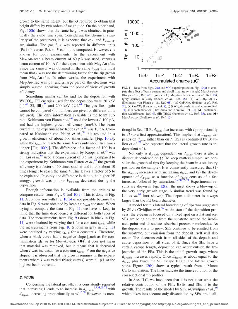
grown to the same height, but the Q required to obtain thatheight differs by two orders of magnitude. On the other hand,Fig. 10�b� shows that the same height was obtained in prac-tically the same time span. Considering the chemical simi-larity of the precursors, it is expected that ��E� and Vmolecule
are similar. The gas flux was reported in different units�Pa l s−1 versus Pa�, so F cannot be compared. However, I isknown for both experiments. In the experiment withMe2-Au-acac a beam current of 60 pA was used, versus abeam current of 10 nA for the experiment with Me2-Au-tfac.Since the same h was obtained in the same tdwell this mustmean that I was not the determining factor for the tip grownfrom Me2-Au-tfac. In other words, the experiment withMe2-Au-tfac was p.l. and a large part of the electrons wassimply wasted, speaking from the point of view of growthefficiency.
Something similar can be said for the deposition withW�CO�6. PE energies used for the deposition were 20 keV�+�,68 25, ���,25 and 200 keV ���.69 The gas flux againcannot be compared �no numbers are given or different unitsare used�. The only information available is the beam cur-rent. Kohlmann-von Platen et al.68 used the lowest I, 100 pA,and had the highest growth efficiency �nm/C�. The beamcurrent in the experiment by Koops et al.25 was 10 nA. Com-pared to Kohlmann-von Platen et al.,68 this resulted in agrowth efficiency of about 500 times smaller �Fig. 10�a��,while the tdwell to reach the same h was only about five timeslonger �Fig. 10�b��. The difference of a factor of 100 is astrong indication that the experiment by Koops et al.25 wasp.l. Liu et al.69 used a beam current of 0.5 nA. Compared tothe experiment by Kohlmann-von Platen et al.,68 the growthefficiency is a factor of 50 times smaller and it took about 10times longer to reach the same h. This leaves a factor of 5 tobe explained. Possibly, the difference is due to the higher PEenergy, growth was p.l., or Vmolecule decreased during thedeposition.
Enough information is available from the articles tocompare results from Figs. 9 and 10�a�. This is done in Fig.11. A comparison with Fig. 10�b� is not possible because thedata in Fig. 9 were obtained by keeping tdwell constant. Whentrying to compare the data in Fig. 11, we have to keep inmind that the time dependence is different for both types ofdata. The measurements from Fig. 9 �shown in black in Fig.11� were obtained by varying the I for a constant tdwell whilethe measurements from Fig. 10 �shown in gray in Fig. 11�were obtained by varying tdwell for a constant I. Therefore,when a black curve has a negative slope �such as for con-tamination ��� or for Me2-Au-acac ����, it does not meanthat material was removed, but it means that h decreasedwhen I was increased for a constant tdwell. From the negativeslopes, it is observed that the growth regimes in the experi-ments where I was varied �black curves� were all p.l. at thehighest beam currents.
2. Width
Concerning the lateral growth, it is consistently reportedthat increasing I leads to an increase in ddeposit,
15,38,68,72 withddeposit increasing proportionally to I.15,68 However, as men-
tioned in Sec. III B, dbeam also increases with I proportionallyto I �to a first approximation�. This implies that ddeposit de-pends on dbeam rather than on I. This is confirmed by Beau-lieu et al.,72 who reported that the lateral growth rate is in-dependent of I.
Not only is ddeposit dependent on dbeam; there is also adistinct dependence on Q. To keep matters simple, we con-sider the growth of tips �by keeping the beam in a stationaryposition on the sample�. It is consistently measured that �1�the ddeposit increases with increasing dbeam and �2� the devel-opment of ddeposit as a function of tdwell consists of a fastincrease, followed by saturation.6,9,68,72–74 Experimental re-sults are shown in Fig. 12�a�; the inset shows a blow-up ofthe very early growth stage. A similar trend was found byLiu et al.69 �not shown�. The deposit diameter is alwayslarger than the PE beam diameter.
A model for this lateral broadening of tips was suggestedby Silvis-Cividjian et al.56 At the start of the deposition pro-cess, the e-beam is focused on a fixed spot on a flat surface.SEs are being emitted from the substrate around the irradi-ated point and dissociate adsorbed precursor molecules. Asthe deposit starts to grow, SEs continue to be emitted fromthe substrate, but emission from the deposit itself will alsooccur. The electrons exit from all sides of the deposit andcause deposition on all sides of it. Since the SEs have acertain escape length, deposition can occur outside the tra-jectories of the PEs. This is the initial growth stage whereddeposit increases rapidly. Once ddeposit is about equal to thedbeam plus twice the SE escape length, the lateral growthstops. Figure 12�b� shows a typical result from a MonteCarlo simulation. The lines indicate the time evolution of thecross-sectional tip profiles.
In Sec. II C, we have seen that it is not clear what therelative contribution of the PEs, BSEs, and SEs is to thegrowth. The results of the model by Silvis-Cividjian et al.,56
which takes into account only dissociation by SEs, are quali-
FIG. 11. Data from Figs. 9�a� and 9�b� superimposed on Fig. 10�a� to com-pare the effect of beam current and dwell time: �gray triangle� Me2-Au-acac�Koops et al., Ref. 67�, �gray circle� Me2-Au-tfac �Koops et al., Ref. 25�,�gray square� W�CO�6 �Koops et al., Ref. 25�, �+� W�CO�6, 20 kV�Kohlmann-von Platen et al., Ref. 68�, ��� CpPtMe3 �Hübner et al., Ref.70�, �x� Co2CO8 �Lau et al., Ref. 8�, ��� WF6 �Hiroshima and Komuro, Ref.71�, ��� contamination �Hiroshima and Komuro, Ref. 71�, ��� contamina-tion �Schiffmann, Ref. 9�, ��� TEOS �Perentes et al., Ref. 35�, and ���Me2-Au-acac �Mølhave et al., Ref. 15�.
081301-10 W. F. van Dorp and C. W. Hagen J. Appl. Phys. 104, 081301 �2008�
Downloaded 15 Sep 2010 to 131.180.130.114. Redistribution subject to AIP license or copyright; see http://jap.aip.org/about/rights_and_permissions

tatively consistent with the experimentally observed lateralgrowth behavior. In the Monte Carlo simulation by Fowlkeset al.,57 a dissociation cross section was used that also takesinto account the contribution of PEs and BSEs. Analysis oftip growth behavior showed that the vertical growth is duemostly to direct dissociation by PEs and the lateral growth isdue mostly to SEs. As the tip grows longer, its sidewall sur-face area becomes larger and the amount of SEs that crossthe substrate-vacuum interface �and contribute to the lateralgrowth� increases. Therefore, although the real cross sectionfor dissociation is unknown, it seems reasonable to assumethat the lateral broadening is due mostly to dissociation bySEs.
Deposits with a small width can be fabricated by using asmall beam and stopping the deposition process before lat-eral widening occurs. In that case, a dot is deposited insteadof a high aspect ratio tip. Stopping the growth process in itsinitial stage influences also the height of the deposits, so inthis regime it is not possible to control the aspect ratio inde-pendently of the width of the deposit merely with the accu-mulated charge. Sub-10-nm structures have been fabricatedwith widths of 8,75,76 5,77 4,78 3.5,79 1.5,80 and even 1.0 nm.81
While for large deposits the deposited mass is identical every
time the experiment is repeated, a significant variation inmass is found for the very smallest deposits. Van Dorp etal.82 deposited arrays of sub-5-nm dots on an a-C substratewith a constant dwell time per array. A typical array is shownin Fig. 13�a� �an annular dark field image obtained in aSTEM�. It is observed that the intensity of the dots �which isproportional to the deposited mass� is not constant over thearray; some of the dots are very bright while other dots arebarely visible. When the average deposit mass is determinedfor each array, a linear dependency on the dwell time isfound �Fig. 13�b��. In Fig. 13�c�, the distribution of depositedmasses is shown for these arrays. The scaling of the arbitraryunits for the deposited mass is identical for Figs. 13�b� and13�c�. Negative values are the result of background subtrac-tions used to determine the deposited mass from the STEMimages. As the dwell time decreases, the width of the distri-bution of masses increases �relative to the average depositedmass� and the distributions become skewed. This behavior isconsistent with the Poisson statistics. The Poisson theory de-scribes the probability that an event occurs during a particu-lar interval given an expected number of discrete occur-rences. In other words, these experiments suggest that the
FIG. 12. The development of the width of an e-beam deposited structure. �a� Experimental results. Inset shows the width development for short times. �b�Result from a Monte Carlo simulation. The lines indicate the time evolution of the cross-sectional profiles. From Ref. 56, Copyright © �2002� by Elsevier.Reprinted with permission from Elsevier: ��� MeCpPtMe3 �Beaulieu et al., Ref. 72�, ��� TEOS �Perentes et al., Ref. 35�, ��� W�CO�6 �Kohlmann-von Platenet al., Ref. 68�, ��� Fe�CO�5 �Shimojo et al., Ref. 74�, ��� CpPtMe3 �Hübner et al., Ref. 70�, and ��� contamination �Schiffmann, Ref. 9�.
FIG. 13. �a� Annular dark field �ADF� image of an array of sub-5-nm dots. Although the dwell time was constant �0.125 s� for all the dots in the array, it isobserved that the dot intensity �equal proportionally to the deposited mass� is not constant. �b� The average mass per array as a function of dwell time. �c� Thedistribution of masses for the different dwell times. The scaling of the arbitrary units for the deposited mass is identical for �b� and �c�.
081301-11 W. F. van Dorp and C. W. Hagen J. Appl. Phys. 104, 081301 �2008�
Downloaded 15 Sep 2010 to 131.180.130.114. Redistribution subject to AIP license or copyright; see http://jap.aip.org/about/rights_and_permissions

deposition process consists of discrete dissociation eventsand this becomes visible during the nucleation stage of adeposit.
The difficulty with these high-resolution experiments isthat the precise experimental conditions are not well known,especially since deposition is done under non-UHV condi-tions �10−3 mbar�. For the micrometer-sized tips we dis-cussed earlier, this is less relevant since for nearly the entiregrowth process the deposit surface is the determining factor,not the substrate surface. For the high-resolution experi-ments, the growth is terminated in the nucleation stage andthe substrate surface and its chemical condition play a majorrole.
3. Composition and morphology
For nearly all experiments with metal-containing precur-sors, the metal content increases with increasing beam cur-rent. Results for Mo�CO�6, CpPtMe3, and Me2-Au-tfac�Refs. 29 and 83–85� and Co2CO8 �Ref. 7� are shown in Fig.14. The metal content for deposits of Me2-Au-acac anddimethyl-hexafluoro-acetylacetonate gold �Me2-Au-hfac�show a similar dependency on beam current as Me2-Au-tfac.An increase in the Co content with beam current was alsoreported in Ref. 8.
The increase in the metal content with beam current thatis observed in Fig. 14 can be due to two parallel processes.First, with an increase in beam current, the time frame inwhich the deposit is exposed to a specific amount of accu-mulated charge decreases. As we have seen earlier, this canlead to a shift from e.l. to p.l. regime. Related to this, theincrease in beam current can induce an increase in the de-sorption of fragments of �initially only partially dissociated�precursor molecules. This can lead to higher concentrationsof nonvolatile �among others metal� components in the finaldeposit. Another mechanism is e-beam induced heating. Aswe have seen in Sec. IV A 1, there are indications that beaminduced heating can lead to a significant rise in temperaturefor tip depositions. A raise in temperature may, for instance,facilitate the desorption of volatile species, as well as changethe dissociation mechanism. We will discuss this in moredetail below, where we present the dependence of the depositmorphology on the beam current.
The morphology of tips can clearly be affected by thebeam current. It is reported for tips deposited fromMe2-Au-acac, Me2-Au-tfac, Me2-Au-hfac, bis-hexafluoro-acetylacetonate copper �Cu�hfac�2�, Mo�CO�6, and CpPtMe3
that at low beam currents, the tips have a smooth shank andare completely amorphous. In contrast, tips deposited withhigh beam currents have an irregular shape and are polycrys-talline, the crystallites being between 2 and 8 nm in size.85
The transition between the two regimes was, for instance,around 60 pA for Me2-Au-tfac. An example of the roughen-ing of the Mo tip surface is shown in Fig. 15�a�. Similarsurface roughening was also observed for hfac-Cu-VMTS�Ref. 86� �Fig. 15�b�� and in a more extreme form forCo�CO3�NO �Fig. 15�c�� and Co2CO8 �Fig. 15�d��. Note thatall deposits in Fig. 15 were created with the beam in spotmode.
In an elaborate study, the development of the morphol-ogy during the growth of tips deposited from Co2�CO�8 wasdetermined and was found to be quite complex.87 At lowbeam currents �20 and 112 pA�, the surface of the tips issmooth and the material consists of nanocomposite material�1–2 nm Co crystals embedded in an a-C- and O-rich ma-trix�. The surface of the longer tips �dwell times of 300–600s� is still smooth, but on the inside a crust and a core form atthe bottom of the tips. This substructure of crust and corebecomes more apparent for deposits from higher beam cur-rents �1.1 and 10 nA�, where it extends along the entirelength of the tip �see Fig. 16�. The crust, consisting of Cocrystals, surrounds the nanocomposite core. When the beamcurrent is increased further to 82 nA, the core/crust structureis absent and only Co-rich crystalline material is found.When the beam current is finally increased to 3 A, thesurface becomes rough and the deposit consists of crystalswith micrometer length growing in a whiskerlike shape to-ward the precursor source �see Fig. 15�d��.
The authors explained these results to a significant extentby e-beam induced heating. Taking into account the limitedthermal conductivity of the deposit material, the heat dissi-pation from the tip to the substrate will be a determining
FIG. 14. The metal content as a function of the beam current. Lines aredrawn to guide the eye: ��� Co2�CO�8 �Utke et al., Ref. 7�, �gray triangle�Me2-Au-tcac �Weber et al., Ref. 29�, �gray circle� CpPtMe3 �Weber et al.,Ref. 85�, and �gray diamond� Mo�CO�6 �Weber et al., Ref. 85�.
FIG. 15. Surface morphologies for high current deposits created with thebeam in spot mode. �a� Deposits from Mo�CO�6. From Ref. 85. �b� Depositsfrom hfac-Cu-VMTS. From Ref. 86. �c� Deposits from �Co�CO3�NO�. Re-printed with permission from Ref. 8. �d� Deposits from Co2CO8. Reprintedfrom Ref. 7. Copyright © 2003 by Elsevier. Reprinted with permission byElsevier.
081301-12 W. F. van Dorp and C. W. Hagen J. Appl. Phys. 104, 081301 �2008�
Downloaded 15 Sep 2010 to 131.180.130.114. Redistribution subject to AIP license or copyright; see http://jap.aip.org/about/rights_and_permissions

factor for the temperature of the tip. At low beam currentsand when the tip is still short, the heat dissipation will besufficient to keep the tip at room temperature. However,when the tip length or the beam current increases, the tem-perature of the tip will be raised above room temperature. At82 nA, the estimated temperature rise is nearly 1 degree,which increases to more than 30 degrees at 3 A for thedescribed experimental conditions. The desorption of volatilespecies can be facilitated by the higher temperature, leadingto a higher metal content. Apart from this, the dissociationmechanism can change at higher temperatures. Co2�CO�8
normally has an endothermal decomposition reaction occur-ring around 100 °C, which is above the estimated tempera-ture reached in tips at the highest beam current. However,this thermal decomposition temperature can be significantlylowered if the activation energy for decomposition is low-ered by autocatalytic effects. In this example, deposited Cowould act as catalyst for the decomposition of Co2�CO�8. Asimilar behavior has been observed for Fe�CO�5 andCr�CO�6.88 These autocatalytic effects can bring the thermaldecomposition temperature to within the temperature rangereached during the described experiments. A similar combi-nation of temperature rise and autocatalytic effect is expectedto be the cause for the development of the deposit fromCo�CO3�NO.
The roughening that was observed at the highest beamcurrents for Me2-Au-acac, Me2-Au-tfac, Me2-Au-hfac,Cu�hfac�2, Mo�CO�6, CpPtMe3, and hfac-Cu-VMTS may bedue to crystallization. As a result of the increase in tempera-ture, volatile fragments desorb more easily and the �in-creased amount of� metal rearranges into small crystals. Thefact that the roughening was observed for quite different pre-cursors indicates again that e-beam induced heating can playa significant role during deposition.
There are also examples where the effect of the beamcurrent is not fundamentally different from the effect of theaccumulated charge. For instance, the deposition of Ni-
containing squares on a carbon substrate �kept at −85 °C�from Ni�C5H5�2.76 At a low accumulated charge, the squareswere open, porous structures and the deposited materialformed a network with �relatively� large openings �Fig.17�a��. Upon continued irradiation, the porous structuresclosed to form �nearly� solid films �Fig. 17�b��. Structurescreated with different beam currents but with a similar accu-mulated charge were in a similar state of transition from anopen structure to a closed film. The fact that accumulatedcharge and beam current were interchangeable indicates thatthe accumulated charge is the only parameter relevant for thedeposition behavior under these specific conditions. An ex-planation for the formation of the open structures was notgiven.
4. Density
Another property that can be measured as a function ofthe beam current is the deposit density. The density of tipsdeposited from tetramethyl ortho-silicate �TMOS�, hfac-Cu-VMTS, and Co2CO8 has been measured for beam currents of0.1, 1, and 100 nA.66 It was found that the density of thedeposit from TMOS is independent of the beam current used.For deposits from hfac-Cu-VMTS both the density and themetal content increased with increasing beam current. Tipscreated with a current of 1 nA had a rough surface. ForCo2CO8, a similar behavior was observed. See Table I for asummary of the results. The bulk density is 8.96 g cm−3 forCu and 8.90 g cm−3 for Co.
The independence of the density and composition of de-posits from TEOS led the authors to the conclusion that thedecomposition is fully due to dissociation by electrons andthat thermal effects are absent. The TEOS precursor mol-ecule dissociates thermally at about 580 °C, which is muchhigher than the calculated temperature rise for a beam cur-
TABLE I. The effect of increasing beam current on the density and metalcontent of deposits from hfac-Cu-VMTS and Co2�CO�8. From Ref. 66.Higher beam currents lead to a higher density and metal content for bothprecursors. Bulk density are 8.96 g /cm3 �Cu� and 8.90 g /cm3 �Co�.
Beam current �nA�Metal content �at. %� Total deposit density �g /cm3�
Cu Co Cu Co
0.1 14 31 2.05 4.21 30 ¯ 4.3 ¯
100 ¯ 73 ¯ 7.2
FIG. 16. Core-crust structure in a tip grown from Co2�CO�8. From Ref. 87.Copyright © 2005 by Wiley-VCH Verlag GmbH & Co. KgaA. Reprintedwith permission by Wiley-VCH Verlag GmbH & Co. KgaA.
FIG. 17. The effect of accumulated charge on the morphology of squaresdeposited from Ni�C5H5�2 at –85 °C. �a� At a low accumulated charge, aporous, open structure is formed. �b� At higher accumulated charges, aclosed, solid film is formed. From Ref. 76. Copyright © 2001 by WorldScientific Publishing Co. Reprinted with permission by World ScientificPublishing Co.
081301-13 W. F. van Dorp and C. W. Hagen J. Appl. Phys. 104, 081301 �2008�
Downloaded 15 Sep 2010 to 131.180.130.114. Redistribution subject to AIP license or copyright; see http://jap.aip.org/about/rights_and_permissions

rent of 1 nA �about 87 °C�. The rough surface in the case ofthe Cu deposits and the large increase in metal content forthe Co deposits indicate thermally assisted deposition �seealso Sec. IV A 3�.
5. Conductivity
Consistent with the increase in metal content, the resis-tivity of wires deposited with the e-beam decreases with in-creasing beam current. The relevant data are summarized inTable II and a typical example of the dependency is shown inFig. 18�a�.
Koops and co-workers29,83–85,89 only gave specific de-tails for experiments with Me2-Au-tfac but mentioned a simi-lar behavior for the other two gold precursors. A wide spreadin resistivities for constant beam currents was found forCo2�CO�8 deposits and this was attributed to the scan methodused to fabricate the Co-containing wires. More details onthis aspect can be found in Sec. V E 2.
For nearly all precursors the resistivity behavior as afunction of the beam current is related to the metal content.As shown in Fig. 14, the metal content consistently increaseswith increasing beam current. This is also consistent with theI-V characteristics, which were determined after depositionat different temperatures for the platinum and the gold wires.The gold wires deposited with the high beam current showOhmic behavior. At lower beam currents, the gold wires con-tain less metal and show nonlinear characteristics, probablyPoole–Frenkel conduction or activated tunneling. The plati-num wires have a lower metal content than the gold wires�see Fig. 14� and show only the nonlinear behavior. An ex-ception to this rule is the experiment with AuCl�PF3�3.92 Thisprecursor yielded pure gold crystals, even at the lowest beamcurrent. The resistivity of wires decreased with increasingbeam current, which is the result of better grain percolation�see Fig. 18�. So this is effectively not so much the result ofthe beam current but rather the result of more accumulatedcharge.
When the conductivity of deposits is measured as a func-tion of accumulated charge, the general trend is that the re-sistance decreases with increasing accumulated charge. Thisis, for instance, the case in measurements by Bruk et al.91
They found that the resistance of wires deposited fromFe3�CO�12 decreases with increasing accumulated charge.However, since the dimensions of the deposits were not re-ported, it is not possible to elucidate the mechanism bywhich the resistance decreased. This can be the result ofmerely a larger wire cross section �a thicker wire can carrymore current� or also of a change in resistivity. The lattercase would imply an accumulated charge-dependent changein material properties.
A more complete experiment was performed withW�CO�6.73 The electrical properties of the deposited wireswere measured in situ for electron doses varying from 0.1�105 to 5�105 C m−2. A fixed potential was applied overthe wire at regular intervals during the deposition. This givesthe development of the current passed through the wire as afunction of the total accumulated charge. For the variousbeam energies used, a constant trend was observed. Initially,the current increment per charge increment increased rapidly,after which the current increment stabilized to a constantvalue. In other words, the conductivity increases nonlinearlyin the initial stage and shows a linear increase later on. Theauthors explained the initial nonlinear stage by a change inthe structure of the wire. The wire starts as a discontinuousline of nuclei and evolves into a continuous wire. In the later
TABLE II. Results from measurements of the resistivity of deposited wires as a function of the beam current.
Material Author�s� Ref. Highest resistivity �beam current� Lowest resistivity �beam current�
CpPtMe3 Weber et al. 29 5.5 cm �200 pA� 1 cm �660 pA�Me2-Au-acac, Me2-Au-tfac, andMe2-Au-hfac
Koops and co-workers 83–85,89 400 cm �100 pA� 2�10−2 cm �900 pA�
Mo�CO�6 2�10−3 cm �¯�Co2�CO�8 Lau et al. 8 5 cm �183 pA� 1.6�10−4 cm �10.7 nA�W�CO�6 Kohlmann-von Platen et al. 90 2�10−2 cm �1000 pA�Fe3�CO�12 Bruk et al. 91 103 cm �11 pA� 4�10−2 cm �232 nA�
FIG. 18. �a� A typical example of the dependence of the resistivity of de-posited wires on the beam current. From Ref. 89. Copyright © 1996 byElsevier. Reprinted with permission by Elsevier. �b� Grains of gold depos-ited from Au�PF3�3. The grains were found for all beam currents, so changesin resistivity as a function of beam current are the result of grain percolation.From Ref. 92.
081301-14 W. F. van Dorp and C. W. Hagen J. Appl. Phys. 104, 081301 �2008�
Downloaded 15 Sep 2010 to 131.180.130.114. Redistribution subject to AIP license or copyright; see http://jap.aip.org/about/rights_and_permissions
stage, when the wire has become continuous, the increase inconductivity is merely the result of an increase in wire crosssection. This implies that the deposition mechanism remainsunchanged during the growth and that it is independent ofthe accumulated charge.
An anomalously high decrease in resistivity is reportedfor squares deposited from WF6.93 The accumulated chargewas varied by varying the pitch between the pixels. With avariation in accumulated charge of a factor of 16, the amountof deposited material increased by a factor of about 10 andthe resistivity decreased from 1.3�103 to 8.4�10−2 cm�a factor of 105�. An explanation for this behavior is notgiven.
B. Electron energy
As was discussed in Sec. II C, experiments have shownthat electrons with energies of about 5 to a few hundred eVcontribute significantly to the growth of deposits. The rela-tive contribution of high-energy electrons to the growth isless clear. It is tempting to think that ��E� can be determinedfor a specific precursor by measuring the deposition yield asa function of the PE energy. This is, however, not as straight-forward as it seems.
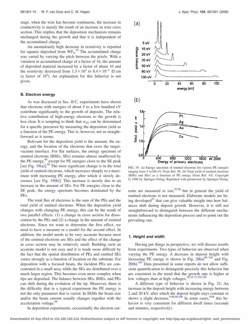
Relevant for the deposition yield is the amount, the en-ergy, and the location of the electrons that cross the target-vacuum interface. For flat surfaces, the energy spectrum ofemitted electrons �BSEs, SEs� remains almost unaffected bythe PE energy,94 except for PE energies close to the SE peak�see Fig. 19�a��.95 The most significant change is in the totalyield of emitted electrons, which increases sharply to a maxi-mum with increasing PE energy, after which it slowly de-creases �see Fig. 19�b��. This increase is mostly due to anincrease in the amount of SEs. For PE energies close to theSE peak, the energy spectrum becomes dominated by thePEs.
The total flux of electrons is the sum of the PEs and thetotal yield of emitted electrons. When the deposition yieldchanges with changing PE energy, this can be the result oftwo parallel effects: �1� a change in cross section for disso-ciation by the PEs and �2� a change in the amount of emittedelectrons. Since we want to determine the first effect, weneed to have a measure or a model for the second effect. Inaddition, the model needs to be very accurate because mostof the emitted electrons are SEs and the effect of the changein cross section may be relatively small. Building such anaccurate model is not easy and it is made more difficult bythe fact that the spatial distribution of PEs and emitted SEsvaries strongly as a function of location on the substrate. Fordeposition with a focused beam, the incident PEs are con-centrated in a small area, while the SEs are distributed over amuch larger region. This becomes even more complex whentips are deposited. The balance between SEs, BSEs, and PEscan shift during the evolution of the tip. Moreover, there isthe difficulty that in a typical experiment the PE energy isnot the only parameter that is varied. In SEMs the beam sizeand/or the beam current usually changes together with theacceleration voltage.96
In deposition experiments, occasionally the electron cur-
rents are measured in situ,97,98 but in general the yield ofemitted electrons is not measured. Elaborate models are be-ing developed57 that can give valuable insight into how bal-ances shift during deposit growth. However, it is still notstraightforward to distinguish between the different mecha-nisms influencing the deposition process and to point out theprevailing one.
1. Height and width
Having put things in perspective, we will discuss resultsfrom experiments. Two types of behavior are observed whenvarying the PE energy. A decrease in deposit height withincreasing PE energy is shown in Fig. 20�a�99–102 and Fig.20�b�.103 Data presented in some reports do not allow suffi-cient quantification to distinguish precisely this behavior butare consistent in the trend that the growth rate is higher atlow voltages than at high voltages.16,22,72,104,105
A different type of behavior is shown in Fig. 21: Anincrease in the deposit height with increasing energy between2 and 20 kV, after which the deposit height stays constant orshows a slight decrease.9,40,68,106 In some cases,9,68 this be-havior is very consistent for different dwell times �secondsand minutes, respectively�.
FIG. 19. �a� Energy spectrum of emitted electrons for various PE energiesranging from 5 to100 eV. From Ref. 95. �b� Total yield of emitted electrons�BSEs and SEs� as a function of PE energy �from Ref. 43�. Copyright© 1998 by Springer-Verlag. Reprinted with permission by Springer-Verlag.
081301-15 W. F. van Dorp and C. W. Hagen J. Appl. Phys. 104, 081301 �2008�
Downloaded 15 Sep 2010 to 131.180.130.114. Redistribution subject to AIP license or copyright; see http://jap.aip.org/about/rights_and_permissions

The dependency of deposit height on PE energy in Fig.20 seems to be consistent with the dependency of the yield ofemitted electrons �BSEs and SEs� on PE energy in Fig.19�b�. Starting at PE energies of a few hundred eV, the depo-sition yield decreases strongly and becomes nearly constantfor PE energies of 10–30 keV. This implies that in theseexperiments the deposit height was mainly dependent on thenumber of emitted SEs.
The results in Fig. 21 seem to be conflicting with thistrend. An increase in the deposit height for higher PE ener-
gies is found, not a decrease. This can possibly be explainedby the size of the interaction volume of scattered electrons inthe target. As Weber et al.29 pointed out, “the major differ-ence when dealing with tips instead of flat substrates is thereduced scattering volume.” At high energies, the probabilityfor a PE to exit the tip after a scattering event is significantbecause the tip is a high and narrow structure. At low ener-gies, scattering occurs mostly within the tip, which can havee-beam induced heating as a result. Depending on the PEenergy, the temperature rise can be as much as 50 °C, asbecomes clear from a model by Randolph et al.40 based onthe effect suggested by Weber et al.29 �see Fig. 22�. Due tothe temperature rise at lower PE energies, the residence time� of adsorbed precursor molecules decreases, which in turnleads to a lower vertical growth rate. This trend is consistentwith the trend found in the experiments by Randolph et al.40
��, Fig. 21�. The effect of beam induced heating would alsoexplain the other results in Fig. 21. Kohlmann-von Platen etal.68 �X, Fig. 21� deposited tips. For the experiments bySchiffmann9 ��� and by Miura et al.106 ���, we have alreadyseen that beam induced heating most likely played a signifi-cant role during variations in the beam current �see Sec.IV A 1�.
The trends in Fig. 21 may be explained with beam in-duced heating, but this explanation raises some questions forthe trends observed in Fig. 20. Bauerdick et al.101 ��, Fig.20� and Beaulieu et al.,72 Ding et al.,16 and Croitoru et al.22
�not shown� also deposited tips or dots and they measured adecrease in growth rate with increasing PE energy. This is incontradiction with the trend we would expect if the effect ofbeam induced heating was significant. For Bauerdick etal.,101 this inconsistency can be explained by a different scanstrategy. The tips were not grown by keeping the e-beam in astationary position on the sample but by giving a series ofshort exposures. Between the exposures, there is time for thethermal energy to dissipate to the underlying substrate, so theeffect of beam induced heating is expected to be much less.It is not possible to use this explanation for the results byBeaulieu et al.,72 Ding et al.,16 and Croitoru et al.22 becausethey grew tips with the beam in spot mode. Due to lack ofdetailed information �local precursor pressure, beam currentsused, etc.� this inconsistency remains unexplained. In con-
FIG. 20. �a� Deposit height as a function of the PE energy shows a similardependence as the generation behavior of SEs. Inset shows the experimentby Hoyle et al. �Ref. 99� between 0.06 and 2 kV: ��� Me3PtCp �Takai et al.,Ref. 100�, ��� W�CO�6 �Bauerdick et al., Ref. 101�, �gray triangle�Me3PtCp �Lipp et al., Ref. 102�, and �gray circle� W�CO�6 �Hoyle et al.,Ref. 99�. �b� The deposit yield in g cm−2 s−1 for diffusion pump oil as afunction of PE energy. From Ref. 103.
FIG. 21. Deposit heights as a function of PE energy: ��� contamination�Schiffmann, Ref. 9�, �X� W�CO�6 �Kohlmann-von Platen et al., Ref. 68�,��� TEOS �Randolph et al., Ref. 40�, and ��� contamination �Miura et al.,Ref. 106�.
FIG. 22. Calculated temperature in tips �60 and 100 nm lengths� comparedto a thin film. From Ref. 40.
081301-16 W. F. van Dorp and C. W. Hagen J. Appl. Phys. 104, 081301 �2008�
Downloaded 15 Sep 2010 to 131.180.130.114. Redistribution subject to AIP license or copyright; see http://jap.aip.org/about/rights_and_permissions
clusion, the combined model of �1� the correlation betweendeposition yield and SE yield and �2� beam induced heatingseems to be valid for most experiments. However, it leavessome experimental results unexplained and the measure-ments are not sufficiently accurate to exclude the contribu-tion from PEs to the growth.
As for the lateral dimensions, all measurements are in-fluenced by the fact that the diameter of the PE beamchanges with changing the electron energy. For the casewhere the beam diameter was measured, it was reported thatthere is little dependence of lateral dimension on e-beamenergy.68
2. Composition and morphology
The results from articles reporting on the influence of thePE energy on the composition of deposits vary quite signifi-cantly. Details about the experiments are often not given, sothe interpretation of the results is difficult. A clear influenceof the PE energy was reported by Weber et al.29 for a numberof precursors �Me2-Au-tfac, Me2-Au-hfac, Me2-Au-acac,Mo�CO�6�. The metal content of tips increased with decreas-ing the PE energy. Numbers �compositions or PE energies�are not given. When irradiating condensated WF6 layers inan Auger SEM, the dissociation rate was found to decreasewith increasing beam energy.107
The behavior observed for the Au and Mo precursorswas explained by the authors as resulting from “the crosssection for inelastic scattering, which is increasing with de-creasing electron energy.”29 Most likely, they refer to thecross section for scattering of PEs, which is larger at lowerPE energies. By this, they imply that the higher metal contentof the tips at lower PE energies is the result of the largerabundance of SEs. In this picture, a decrease in PE energy isequivalent to increasing the accumulated charge per unittime. This mechanism would be consistent with the behaviorobserved for WF6.
In several other studies, no influence of the PE energywas found. Folch and Servat64 reported that the compositionof deposits from Me2-Au-hfac was constant for PE energiesbetween 10 and 40 keV. For contamination deposits, the ratiobetween sp2- and sp3-bonded C was measured for PE ener-gies between 3 and 20 keV.16 Variations were below the un-certainty level of about 10% of the measurement technique�electron energy loss spectrometry �EELS��. The diffractionpatterns of 50 nm thick films deposited from W�CO�6 ob-tained in the TEM showed no visible difference when fabri-cated with different beam energies.73 Also the composition ofrectangles deposited from �RhCl�PF3�2�2 was found to beindependent of the PE energy.108
The independence of the composition from PE energyfor deposits Me2-Au-hfac found by Folch and Servat64 issurprising since Weber et al.29 did find a dependence for thesame precursor.29 According to Folch and Servat,64 the ob-served lack of dependence “rules out the possibility that sub-strate heating by the impinging electrons plays a significantrole in the deposition mechanism, as the heating effect in-creases with increasing energy.” It is not straightforward tosee why this is so because it is not mentioned whether tips orsquares are deposited. This would imply that in the results by
Weber et al.29 e-beam induced heating did play a significantrole. Keeping in mind the discussion in Sec. IV A 3 and thefact that Weber et al.29 deposited tips, this sounds plausible.However, lack of information prevents conclusions that aremore definite.
3. Conductivity
The inconsistency in the effect of the PE energy on thecomposition of deposits is also found for measurements ofthe conductivity. It was found for W�CO�6 by Hoyle et al.99
that the conductivity increases with decreasing energy �var-ied between 500 eV and 20 keV�. This trend was confirmedfor W�CO�6 lines deposited with energies between 20 and 30keV by Kohlmann-von Platen et al.90 In contradiction withthese results, the conductivity of lines deposited fromtrimethyl-platinum-methylcyclopentadienyl �MeCpPtMe3�decreased by a factor of 3 when the PE energy increasedfrom 5 to 20 keV.109
These inconsistent results are difficult to explain. In allthree cases, the deposits were created by scanning the pattern�lines or squares� a large number of times to obtain sufficientheight. This, and the fact that low aspect ratio structures wereused �instead of tips, for instance�, makes the occurrence ofe-beam induced heating in any of the experiments not verylikely. Hoyle et al.99 explained their results by assuming thatSEs play a major role in the deposition process. At lower PEenergies, precursor molecules undergo more collisions withelectrons, increasing the desorption of volatile species andincreasing the metal content. The same mechanism wouldhave occurred for the Pt precursor, so that does not explainthe difference. The contrasting results may be due to differ-ence in precursor chemistry, but again, a mechanism is noteasy to see.
C. Conclusions
Regarding the vertical growth of deposits, measurementsof the effect of the current density are mostly consistent witheach other and with the existing growth model. The plot thatgives most insight into the growth process is a measurementof h as a function of J �or Vdeposit as function of I�. The e.l.and p.l. regimes can be identified and explained quantita-tively �to some extent� for experimental results. An experi-ment with contamination indicates that a high J �or I� canlead to e-beam induced heating, which significantly affectsthe vertical growth rate. Often, the vertical growth is re-ported in terms of h as a function of Q or tdwell. For most ofthese cases, too much information is missing �such as thelocal precursor flux� to explain the observed behavior quan-titatively and sometimes even qualitatively. Contradictory re-sults were found for experiments where the influence of thePE energy on the vertical growth was studied. These contra-dictions could be explained largely with a combination of thegrowth model and beam induced heating, but this approachleaves some results unexplained. Unfortunately, there is notenough information available to find out why.
Concerning the lateral growth, this is consistently foundto be independent of J and the PE energy. Instead, ddeposit
depends on dbeam and on Q �for growth in the e.l. regime�
081301-17 W. F. van Dorp and C. W. Hagen J. Appl. Phys. 104, 081301 �2008�
Downloaded 15 Sep 2010 to 131.180.130.114. Redistribution subject to AIP license or copyright; see http://jap.aip.org/about/rights_and_permissions

and shows a fast initial increase followed by saturation. Thisbehavior can be explained by dissociation by SEs emittedfrom the growing deposit itself. Deposits with a ddeposit assmall as 1.0 nm have been created by stopping the growth inthe fast increase stage. At these dimensions, the number ofmolecules per deposit is so small that the effect of the count-ing statistics becomes visible.
For metal-organic precursors, an increasing J generallyleads to an increase in metal content, conductivity, and den-sity. Additionally, the deposit surface changes from smoothto rough. This is partially due to an increased degree of elec-tron induced dissociation and partially due to a change indissociation mechanism. At a high J beam induced heatingcan occur. If the precursor has a thermal decomposition tem-perature within the range of temperatures that can be reachedby beam induced heating, the dissociation mechanism maynot be merely electron induced but can also be thermallyinduced. For precursors with a thermal decomposition tem-perature well above temperatures reached with beam inducedheating �such as TEOS�, no effect of J is observed. Inconsis-tent results were found for the effect of the PE energy on thecomposition, morphology, and conductivity. It is suggestedthat beam induced heating or the amount of emitted SEsplayed a significant role during these experiments, but lackof information prevents definite conclusions.
V. SCAN PATTERN AND SCAN STRATEGY
One of the advantages of EBID is that two-dimensionalas well as 3D patterns can be defined. Apart from the prop-
erties of the beam �size, current, energy�, the scan pattern aswell as the scan strategy can have a significant influence onthe deposit. A number of parameters are defined in the scanstrategy. In the case of lines, for instance, the line length andthe scan speed are most apparent parameters. Related to thisis the period between subsequent visits of the same point onthe substrate. This is known under several names: “repeattimes,” “loop times,” “refresh times,” “line times,” or “delaytimes.” We will use the term loop time. Apart from thesevariables, the dose per scan can also be varied. For digitaldeflection systems, this is the number of pixels per line.These parameters can be interconnected �for instance, thescan speed and the loop time�, so it requires some care toperform and describe experiments in such a manner that con-clusions can be drawn from the results.
A. Scan pattern
1. Height and width
Until now, we have mainly discussed the deposition oftips by spot irradiation. Although this is perhaps conceptuallythe simplest deposition experiment, we have already seenthat this can lead to a quite complex behavior. The factwhether the process is e.l. or p.l. can significantly influencethe growth rate, the composition, and the morphology. Herewe will see that it can also affect the height distribution ofthe deposit. In the extreme case, growth is p.l. almost di-rectly from the start. An example is the use of residual gas asa �carbon� precursor. If a large beam is used, nonuniform
FIG. 23. �Color online� �a� Contamination ring as a result of broad beam illumination. From Ref. 111. Copyright © 1978 by Elsevier. Reprinted withpermission by Elsevier. �b� Height profile and �c� contamination ring. From Ref. 110. �d� The growth rate as a function of the normalized distance with thebeam in spot mode for different growth regimes, calculated from a continuum model. From Ref. 112. The p.l. regime is called diffusion limited. �e� Same asin �d� but now calculated from a Monte Carlo simulation. From Ref. 113. Copyright © 2007 by IOP Publishing Ltd. Reprinted with permission by IOPPublishing Ltd. The deposit profiles for the p.l. regime �——� and e.l. regime �— —� are shown, together with the e-beam profile �— · —�.
081301-18 W. F. van Dorp and C. W. Hagen J. Appl. Phys. 104, 081301 �2008�
Downloaded 15 Sep 2010 to 131.180.130.114. Redistribution subject to AIP license or copyright; see http://jap.aip.org/about/rights_and_permissions

height distributions are found, as, for instance, reported byFourie110 and Reimer and Wächter.111 They studied contami-nation growth in early electron optical systems. When irra-diating a substrate with a beam with a diameter of somemicrometers, deposition of carbon occurred only along theedge of the beam and not in the center. Typical deposit heightprofiles are shown in Figs. 23�a�–23�c�.
The explanation for this behavior is as follows.111 IfgF /N0��J the area under the beam will quickly becomedepleted of mobile precursor molecules. The supply of newmolecules will have to come from outside the irradiated area.If direct adsorption from the gas phase is the prevalent sup-ply mechanism, all locations under the e-beam have an equalprobability for adsorption �and dissociation�. If surface dif-fusion is the prevalent supply mechanism, molecules willdiffuse from the outside inwards and will be pinned downbefore they reach the center of the irradiated area. The factthat a ring structure is found indicates that �for these particu-lar experimental conditions� surface diffusion was the preva-lent supply mechanism.
The effect of the two growth regimes can be reproducedwell with theoretical models. Results from a continuummodel developed by Utke et al.112 and a Monte Carlo simu-lation developed by Smith et al.113 are shown in Figs. 23�d�and 23�e�, respectively. The p.l. regime is called diffusionlimited in Fig. 23�d�. That the ring shape is not visible in Fig.23�e� is probably because a very small beam diameter wasused.
Similar results were later found experimentally in simi-lar conditions for lines and squares. The middle sections oflines �deposited from contamination, several micrometerwide� showed a different height profile than the endsections.114
Figure 24�a� shows an atomic force microscopy �AFM�
image and Fig. 24�b� shows the height profiles. This indi-cates that the precursor supply is mainly by surface diffusion.The end sections have a larger area to draw hydrocarbonsfrom than the middle section and therefore the end sectionsbecome higher than the middle section. The theory of supplyby diffusion was tested with a dedicated experiment. Arounda spot on the substrate, four lines were scanned that con-nected to make a square. The spot and the surrounding lineswere irradiated in alternating sequence. While keeping thescan strategy �total accumulated charge, dwell times, looptimes� constant for the dot in the middle, the influence of thepresence and the length of the four lines was studied �seeFig. 24�c� for a schematic representation�. The height of anisolated dot was 209 nm, and this decreased to 139, 133, and111 nm for squares of 80�80, 60�60, and 40�40 m2,respectively. This result is consistent with the theory that theprimary supply mechanism is diffusion over the surface.
The same conclusion was drawn by Ding et al.16 afterdepositing squares using paraffin as a precursor. A smallamount of paraffin was placed on a cleaned Si substrate andabout 35 m away a square of several micrometer lengthand width was defined. The height profile of the resultingstructure is shown in Fig. 24�d�. The edges are thicker thanthe middle, and the four corners are again higher than theedges. This is consistent with the diffusion picture sketchedabove, where the supply of molecules is largest for the cor-ners and smallest for the middle of the square.
2. Composition and morphology
We have seen strong indications in Sec. IV A 1 thate-beam induced heating can play a significant role in thedeposition process. This happens when the energy input bythe e-beam is larger than the energy dissipation from the
FIG. 24. Height profiles of deposits indicating that surface diffusion is the prevalent precursor supply mechanism. �a� AFM image of a line several micrometerwide. The line end has a different height profile than the line middle. �b� The absolute height profiles. �c� Test pattern to study the effect of surface diffusion.�d� Scanned square, where paraffin was used as precursor. �a�–�c� are from from Ref. 114. �d� is from Ref. 16.
081301-19 W. F. van Dorp and C. W. Hagen J. Appl. Phys. 104, 081301 �2008�
Downloaded 15 Sep 2010 to 131.180.130.114. Redistribution subject to AIP license or copyright; see http://jap.aip.org/about/rights_and_permissions
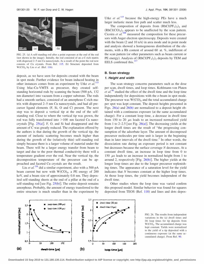
deposit, as we have seen for deposits created with the beamin spot mode. Further evidence for beam induced heating inother instances comes from an experiment by Utke et al.115
Using hfac-Cu-VMTS as precursor, they created self-standing horizontal rods by scanning the beam �500 pA, 132nm diameter� into vacuum from a copper substrate. The rodshad a smooth surface, consisted of an amorphous C-rich ma-trix with dispersed 2–5 nm Cu nanocrystals, and had all pre-cursor ligand elements �F, Si, O and C� present. The nextstep was to deposit a vertical tip at the end of the self-standing rod. Close to where the vertical tip was grown, therod was fully transformed into �100 nm faceted Cu nano-crystals �Fig. 25�a��. F, O, and Si had disappeared and theamount of C was greatly reduced. The explanation offered bythe authors is that during the growth of the vertical tip, theamount of inelastic scattering becomes much higher thanduring the growth of the �relatively thin� self-standing rodsimply because there is a larger volume of material under thebeam. There will be a larger energy transfer from beam totarget and due to the poor thermal conductivity there will atemperature gradient over the rod. Near the vertical tip, thedecomposition temperature of the precursor can be ap-proached and faceted Cu crystals are the result.
Liu et al.116 did a similar experiment, also with a 500 pAbeam current but now with W�CO�6, a PE energy of 200keV, and a beam size of approximately 0.8 nm. They depos-ited self-standing sheets at the end of a pillar at the end of aself-standing rod �see Fig. 25�b��. The entire deposit remainsamorphous. Probably, the amount of energy transferred to theentire structure is much smaller than in the experiment by
Utke et al.115 because the high-energy PEs have a muchlarger inelastic mean free path and scatter much less.
The composition of deposits from �RhCl�PF3�2�2 and�RhCl�CO�2�2 appears to be unaffected by the scan pattern.Cicoira et al.108 measured the composition for these precur-sors with Auger electron spectroscopy. Deposits were createdwith the beam �2 and 10 nA� in area mode and in point modeand analysis showed a homogeneous distribution of the ele-ments, with a Rh content of around 60 at. %, indifferent ofthe scan pattern �or other parameters such as beam current orPE energy�. Analysis of �RhCl�PF3�2�2 deposits by TEM andEELS confirmed this.117
B. Scan strategy
1. Height and width
The scan strategy concerns parameters such as the doseper scan, dwell times, and loop times. Kohlmann-von Platenet al.90 studied the effect of the dwell time and the loop timeindependently for depositions with the e-beam in spot mode.The precursor was W�CO�6 and the total accumulated chargeper spot was kept constant. The deposit heights presented inFigs. 26�a� and 26�b� are normalized to a deposit height ob-tained with a continuous exposure �at the same accumulatedcharge�. For a constant loop time, a decrease in dwell timefrom 150 to 20 s leads to an increased normalized yieldfrom 1 to 2–2.5 �see Fig. 26�a��. The decreasing yields at thelonger dwell times are the result of “the progressing con-sumption of the adsorbate layer. The amount of decomposedprecursor molecules per time unit is larger in the beginningthan in later intervals of the dwell time.” In other words, thedissociation rate during an exposure period is not constantbut decreases because the surface coverage N decreases. At aconstant dwell time, an increase in loop time from 0 to150 s leads to an increase in normalized height from 1 toaround 2, respectively �Fig. 26�b��. The higher yields at thelonger loop times are due to the longer precursor replenish-ing times. The appearance of a saturation level for the yieldindicates that N becomes constant at the higher loop times.At those loop times, the yield becomes independent of thedwell time.
Other studies where the loop time was varied confirmthis proposed model. Similar behavior was found for squaresdeposited from TEOS �Ref. 118� and lines and dots depos-
FIG. 25. �a� A self-standing rod after a point exposure at the end of the rod�not shown in the image�. Initially, the rod consisted of an a-C-rich matrixwith dispersed 2–5 nm Cu nanocrystals. As a result of the point the rod nowconsists of Cu crystals. From Ref. 115. �b� Structure deposited fromW�CO�6 by Liu et al. �Ref. 116�.
FIG. 26. The results from independentvariations in the �a� dwell times and�b� loop times for tip deposits fromW�CO�6. The accumulated charge waskept constant. Yields were normalizedto the yield of a tip deposited with acontinuous exposure �at the same ac-cumulated charge�. From Ref. 90.
081301-20 W. F. van Dorp and C. W. Hagen J. Appl. Phys. 104, 081301 �2008�
Downloaded 15 Sep 2010 to 131.180.130.114. Redistribution subject to AIP license or copyright; see http://jap.aip.org/about/rights_and_permissions

ited from contamination.114 Beaulieu et al.72 did not giveexact numbers but did report that an increase in loop time bya factor of 4 gives an increase in vertical growth rate of afactor of 4. It is interesting that, for the different experi-ments, saturation of the deposition yield for the longer looptimes occurs at different time scales. While saturation occursin the order of 100–200 s in the experiments byKohlmann-von Platen et al.,90 Lipp et al.118 found timescales of 10–20 ms and Amman et al.114 found time scales inthe order of 20 s. This must be due to differences in F.Amman et al.114 used contamination as a precursor and aretherefore dependent on surface diffusion as supply mecha-nism �see also Sec. IV A 1�. Kohlmann-von Platen et al.90
and Lipp et al.118 both reported an F of1017 molecules cm−2 s−1. The difference between the resultsby Kohlmann-von Platen et al.90 and Lipp et al.118 are pos-sibly due to the sticking coefficients of the precursors�W�CO�6 and TEOS, respectively�.
Results are less consistent when the dwell time is varied.Sanchez et al.119 mentioned �without giving absolute num-bers� that short dwell times are beneficial for a high growthrate when scanning squares, similar to what Kohlmann-vonPlaten et al.10 found. On the other hand, Lipp et al.118 foundthat the effect on the deposition yield was less pronouncedthan in the experiments by Kohlmann-von Platen et al.90
This may be because the dwell times may have been tooshort. The current density Lipp et al.118 used was smallerthan what Kohlmann-von Platen et al.90 used �10 instead of75 A cm−2�, which means that one would expect that deple-tion occurs at longer dwell times �i.e., the curve in Fig. 26�a�shifts to the right�. However, Lipp et al.118 used shorter dwelltimes �0.5–2 s�, where depletion may not have occurred atall. Beaulieu et al.72 reported that the dwell time did notappear to be significant at all. This can perhaps be explainedby the fact that Beaulieu et al.72 used dwell times in therange of 5–500 ms, much longer than in the experiments byKohlmann-von Platen et al.90 or Lipp et al.118 It is possiblethat the deposition area was depleted from precursor mol-ecules even at the smallest dwell times.
In some cases, the way the experiment is performed doesnot allow a full interpretation of the influence of dwell andloop times. For instance, when scanning a line with constantlength and with constant total accumulated charge, the doseper scan �in C m−2� was varied.120 Effectively, this results inthe simultaneous variation in both the dwell time per pointand the loop time. Another example is a variation in the “linedose” �in C cm−1� without keeping the total accumulatedcharge constant.71 The simultaneous variation in several pa-rameters prevents the determination of the influence of indi-vidual parameters such as dwell and loop times.
There are two reports of a dependency of the line widthon the dwell and loop times. For contamination lines, a de-crease in the loop time leads to a different height profile.114
Figure 27�a� shows profiles of lines written with loop timesof 100.2, 30.6, 20.2, and 5.2 s �constant dwell time�; a sche-matic is shown in Fig. 27�b�. At the shorter loop times, thesurface diffusion length is not sufficient to supply the centralpart of the line with contamination molecules and depositiononly occurs at the edge of the structure. Beaulieu et al.72
mentioned that a combined increase in dwell time and looptime gave a definite decrease in line width. However, sincefurther details are not mentioned, it remains unclear why thisis so.
2. Conductivity
Hoyle et al.120 have written 30 m lines with W�CO�6
with a total dose of 5�105 C m−2, while the scan speed andcorresponding number of scans were varied. Effectively, thisresults in a corresponding simultaneous variation in both thedwell time per point and the loop time. Measurements of theresistivity show two regimes. For fast scans �doses less thanabout 500 C m−2, relatively short dwell and loop times�, ahigh resistivity deposit is found, while for slow scans �doseslarger than about 5000 C m−2, relatively long dwell and looptimes� a low resistivity is found. The authors described thesetwo regimes as “electron-flux limited” and “gas-flux lim-ited.” In the gas-flux limited regime, “each deposited mol-ecule undergoes a larger number of electron collisions whileat the surface, and this may result in additional desorption ofCO” and therefore contribute to a lower resistivity.
This model is confirmed by experiments by Hiroshimaand Komuro71 for WF6 and Utke et al.121 for Me2-Au-tfac.Hiroshima and Komuro71 reported that a single slow scanyielded a line with lower resistivity than 200 fast scans.Similarly, Utke et al.121 kept the total line dose constant andtried a single slow pass �9 nm s−1� versus 6�105 fast passes�500 m s−1� per line. The resistivity is about 60 timeshigher for the fast scan �with relatively short dwell and looptimes� than for the single slow scan �with relatively longdwell and loop times�.
In conclusion, the trend seems to be that the effect of thescan strategy on the conductivity is dependent on the ratiobetween electrons and deposited molecules. If this ratio in-creases �more electrons per deposited molecule�, the disso-ciation of molecules will be more complete and the conduc-tivity will increase.
C. Scan speed
If a line is scanned by the e-beam in a single pass andthe scan speed is increased from 0 nm/s onwards, a transitionwill be observed from pillar growth to line deposition. Firststudied by Koops et al.67 and Mølhave et al.,122 the evolutionof the growth behavior is well presented in Figs. 28�a� and28�b�.123 As the scan speed is increased �increasing from a tol�, the structures become increasingly inclined. At the sametime, a second deposit starts to grow on the substrate, which
FIG. 27. �a� The height profiles of contamination lines deposited with dif-ferent loop times �at constant dwell time�. The loop times are indicated inthe figure. From Ref. 114. �b� Schematic of the setup.
081301-21 W. F. van Dorp and C. W. Hagen J. Appl. Phys. 104, 081301 �2008�
Downloaded 15 Sep 2010 to 131.180.130.114. Redistribution subject to AIP license or copyright; see http://jap.aip.org/about/rights_and_permissions

becomes visible from pillar d or e onwards in Fig. 28�a�. Asthe pillar becomes increasingly inclined, the second depositcan also “take off” from the substrate �illustrated by k and lin Fig. 28�a��. If the scan speeds are increased even further,periodic fencelike structures and finally solid lines �see Fig.28�c�� are deposited.124,125 Based on an extensive study, itwas found that the growth of these secondary structures andthe periodic growth is caused by the decreasing precursorsupply efficiency to the end of the inclined pillar. As a resultof the increased diffusion path, the flux of precursor mol-ecules reaching the end of the pillar decreases and the tipbecomes thinner and narrower. From a certain scan speedonwards, the e-beam can penetrate the inclined pillar andcreate a second deposit on the substrate. As the primary pillarbecomes thinner and thinner, more electrons penetrate andthe vertical growth rate of the secondary structure increases.Finally, the primary and the secondary structure meet. Theprocess then repeats itself. If the scan speed is increased, thethinning of the primary pillar and the growth of the second-ary structure start earlier and the periodicity becomessmaller. Finally, a flat line is scanned.
A few other cases are known of secondary structuresgrowing parallel to freestanding primary structures.122,126 Itis likely that this is caused by the PEs getting through to theunderlying substrate.
The influence of the scan speed has also been studied forvery high-resolution ��10 nm width� self-standing struc-tures. When the e-beam is scanned over a hole, a self-standing rod will grow. It is consistently reported that thewidth of the rods �dimension perpendicular to the e-beamand the scan direction� decreases with increasing speed ofthe e-beam.127,128 See also Fig. 29�a�. The width at scanspeeds above 10 nm s−1 saturates at 7–10 nm. The widthevolution of the rods is roughly similar to the evolution ofdots as proposed by Silvis-Cividjian et al.56 If the e-beamirradiates each position on the rod for a longer time, moreSEs are emitted at the side of the rod and it becomes wider.The 1/�scan speed� relationship seems to indicate that theamount of material that is deposited per unit time remainsconstant for scan speeds up to 10 nm s−1.
Apart from the width of the rods, the angle of inclinationof the rods also appears to be dependent on the scan speed.127
The angle between the substrate and rod decreases with in-creasing scan speed. For scan speeds of 0.8, 4, and24 nm s−1, the angles of inclination were +55°, 0°, and−15°, respectively. The authors explained this with the �digi-tized� step sizes of the e-beam, which are made smaller when
the scan speed is decreased. It is assumed that a Gaussianshaped e-beam �0.8 nm diameter� creates Gaussian shapeddeposits at each step of the e-beam. In Fig. 29�c�, a sche-matic is depicted for three scan speeds: 0.8, 4, and24 nm s−1. At every new step, the beam is positioned some-where on the slope of the already existing deposit. For a low,intermediate, or high scan speed, this position is above �po-sition A�, around �position B�, or below �position C� theinitial height of the substrate. Hence, the inclination of therods is dependent on the scan speed. Similar results werefound by Mølhave et al.122 for depositions in an environmen-tal SEM.
D. Writing direction
1. Height
It has been observed that the writing direction with re-spect to the precursor source can be of influence on the ver-tical growth rate. The effect of the position of the gas nozzlewas tested by depositing lines at a constant speed.129 At thestarting position of the line, a tip with constant height wasdeposited. The line was written from this tip toward thenozzle or from this tip away from the nozzle �see Fig. 30�.Considerably more material was deposited when the beamwas scanned toward the gas nozzle than when it was scannedaway from the gas nozzle, although the final line height re-mains constant. This dependency of the vertical growth rateon the orientation with respect to the nozzle was also foundfor other patterns. The proposed explanation is that the cov-erage of precursor molecules is not constant over the surfaceof the tip. The side of the tip facing the gas nozzle has ahigher coverage of precursor molecules than the side of thetip away from the gas nozzle. This shadowing effect causesthe lower growth rate for the line that was written away fromthe gas nozzle. Estimations of the precursor coverage N inthe shadowed areas based on the kinetic theory of gas quan-titatively agree with the experimental results.
A similar dependency was observed in an experimentwhere the precursor supply was mainly by diffusion over thesurface instead of through the gas phase.16 A small amount ofparaffin was placed on a Si wafer and used as a precursor forthe deposition of a square about 35 m away. A completeAFM image of this square is shown in Fig. 24�d� and theheight profile over line A in that figure is shown in Fig. 31. Itshows that the side closest to the paraffin source �O� ishigher than the side furthest away from the paraffin source�O��.
FIG. 28. ��a� and �b�� The inclination of tips as a function of the scan speed. From Ref. 123. At sufficiently large scan speeds, secondary deposits start to grow�starting from pillar e and f onwards�. �c� At increased scan speeds, fencelike structures and finally solid lines are deposited. From Ref. 124.
081301-22 W. F. van Dorp and C. W. Hagen J. Appl. Phys. 104, 081301 �2008�
Downloaded 15 Sep 2010 to 131.180.130.114. Redistribution subject to AIP license or copyright; see http://jap.aip.org/about/rights_and_permissions

2. Composition and morphology
The position of the gas nozzle with respect to the depositcan influence the deposit morphology, as can be seen in lat-eral cross sections taken from tips deposited fromCo2�CO�8.87 For the image in Fig. 32, the gas nozzle waspositioned on the right side. A cobalt-poor region is found inthe area toward the gas nozzle, consisting of Co nanocrystalsembedded in a matrix of a-C. This cobalt-poor region isasymmetrically surrounded by a crust with larger Co grains�see also Fig. 16�. In Sec. IIIB2, it was explained that thecore/crust effect was probably due to e-beam induced heat-ing. The authors suggested that the Co-poor region is di-rected toward the gas nozzle as a consequence of a coolingeffect of the arriving precursor molecules. The cooling effectis absent on the side of the tip that is shadowed from the gasnozzle and there beam induced heating leads to the larger Cograins in the surrounding crust. The shadowing effects canalso lead to void formation in tips deposited with a highbeam current �82 nA�.
E. Proximity effects
1. Deposit location
A proximity effect is strictly speaking not really a pa-rameter that can be varied, such as the beam current or thePE energy. However, a significant number of proximity ef-fects have been reported until now for EBID, arising fromdifferent causes. Since these effects can significantly influ-ence the final deposit shape or deposit distribution over thesurface, we feel that a dedicated section is justified. Proxim-ity effects are well known in resist based e-beam lithography.It is usually caused by BSEs and presents itself as an extraand unintentional exposure of the resist layer surrounding theirradiated areas. Several types of proximity effects have al-
FIG. 29. �a� Width dependence of self-standing rods as a function of thescan speed. �b� The dependence of the angle of inclination on the scanspeed. �c� Schematic of the effect of changing the scan speed. From Ref.127.
FIG. 30. The effect of the writing direction with respect to gas nozzle. A tip was deposited, followed by a line deposition. When the line was written awayfrom the nozzle, significantly less material was deposited than when the line was written toward the nozzle. From Ref. 129. Copyright © 2005 by Elsevier.Reprinted with permission by Elsevier.
FIG. 31. Height profile of a square, demonstrating the influence of thedirection of the precursor supply. The precursor source was located about35 m away, on the left side of O. From Ref. 16.
081301-23 W. F. van Dorp and C. W. Hagen J. Appl. Phys. 104, 081301 �2008�
Downloaded 15 Sep 2010 to 131.180.130.114. Redistribution subject to AIP license or copyright; see http://jap.aip.org/about/rights_and_permissions

ready been reported for EBID, where matters are more com-plicated because the irradiated targets are growing and there-fore change in shape.
An effect similar to that in e-beam lithography, herecalled the “BSE proximity effect,” was reported by, for in-stance, Lau et al.,8 Boero et al.,31 and Edinger et al.26 Extradeposition can be observed as a halo around the base of tips�Fig. 33�a�� or around lines �Fig. 33�b��. In Fig. 33�b�, thewidth of the halo was much larger on the SiO2 than on the�prefabricated� pure Au pads. This is consistent with thelarger backscatter range of the incident PEs for SiO2 than forAu. Since the backscatter range is �among others� dependenton the energy of the incident PEs, working at low accelera-tion voltages is beneficial in reducing this proximity effect.
There is a proximity effect that is similar to the BSEproximity effect except for the fact that it causes parasiticdeposition on larger length scales. It was observed when atall tip was grown on a substrate on which small Si particleswere scattered.65 Parasitic deposition was observed in theentire area surrounding the tip but not in locations directlybehind the Si particles �see Fig. 34�a��. This excludes theBSE proximity effect since that causes radially decreasingyet uniform parasitic deposition. Here, the parasitic deposi-tion is caused by the spraying of high-energy electrons thatare scattered in the growing tip. These electrons have a muchlarger range than BSEs and will be blocked by obstacles intheir path �such as Si particles�. Although strictly speakingany electron that has undergone a scattering event and has anenergy �50 eV is defined as a BSE, this effect is here calledthe “FSE proximity effect.” A few articles report parasiticdeposition that can probably be attributed to this proximityeffect. Zhang et al.130 observed parasitic deposition on verythin electron transparent membranes, where the substrate istoo thin for BSEs to play a significant role �see Fig. 34�b��.Secondary ion mass spectroscopy �SIMS� performed by Go-pal et al.109,131 showed that Pt was distributed around a talltip in an area many tens of micrometer wide �see Figs. 34�c�and 34�d��. They explained this by thermally assisted diffu-sion of dissociated species over the surface. Under influenceof beam induced heating of the grown tip, the lifetime ofdissociated precursor molecules would then be sufficient to
diffuse over large distances. We think, in the light of theabove-described experiments, that it is more likely that theparasitic deposition is the result of the FSE proximity effect.
Several authors reported a type of proximity effectwhere parasitic deposition occurred on already existingstructures when new deposits were created in the close vi-cinity. This was found for self-standing rods,132,133 dots,8 andtips.122 Aristov et al.133 observed that the upper rod in Fig.35�a� thickened as result of the fabrication of the lower rod,even though the deposition parameters were identical. Lau etal.8 deposited an array of dots with constant dwell time andobserved that the dots written earlier in the array were con-siderably thicker �Fig. 35�b�, array written from top to bot-tom, left to right�. Aristov et al.133 suggested that the extradeposition is caused by SE spraying from the structure that isbeing fabricated. This effect is here called the “SE proximityeffect.” In reality, the energy of the electrons is not measuredand in principle, this unintentional growth can also be causedby �50 eV electrons which are scattered or generated in thenewly grown structure. It is therefore possible that there is nofundamental difference between the FSE and the SE proxim-ity effects.
Hiroshima and Komuro71 and Van Dorp et al.134 reportedstudies on a proximity effect that is different from the prox-imity effects discussed until now in the sense that it affectsthe structures that are being written instead of the structuresthat are already present at the time of writing. The amount of
FIG. 32. Lateral cross section demonstrating the influence of the direction ofthe gas nozzle. A Co-poor region is found off center, on the side facing theprecursor supply. From Ref. 87. Copyright © 2005 by Wiley-VCH VerlagGmbH & Co. KgaA. Reprinted with permission by Wiley-VCH VerlagGmbH & Co. KgaA.
FIG. 33. Examples of a proximity effect as it is known in e-beam lithogra-phy. �a� A halo around a deposited tip. From Ref. 8. In the article, nocomment is given on the presence of the white line in the image. �b� A haloaround deposited lines. From Ref. 86. Reprinted with permission from au-thor. The width of the halo is larger on the Si than on the Au.
081301-24 W. F. van Dorp and C. W. Hagen J. Appl. Phys. 104, 081301 �2008�
Downloaded 15 Sep 2010 to 131.180.130.114. Redistribution subject to AIP license or copyright; see http://jap.aip.org/about/rights_and_permissions

material that is deposited under the e-beam �excluding para-sitic deposition as a result of the proximity effects describedabove� appears to be larger when the e-beam irradiates theside of an already existing structure than when it irradiates aflat area on the substrate. Hiroshima and Komuro71 observeda surprisingly high vertical growth rate when depositing linesin a single slow line scan �Fig. 36�a��, while Van Dorp etal.134 observed an increase in the amount of deposited mate-rial when writing parallel lines with constant dwell time at aspacing of roughly the same magnitude as the width of thelines �Fig. 36�b��. The amount of deposited material is foundto be proportional to 1 /sin �, where � is the angle betweenthe substrate and the e-beam. The effect is called here the“slope dependent proximity effect.” Van Dorp et al.134 founda good �qualitative� correlation between the SE emissionfrom the irradiated structure and the extra amount of growthdue to the proximity effect. However, this does not necessar-ily imply that the extra deposition is caused by enhanced SEemission from the sidewall of the irradiated structure. Whenone pictures the adsorbed precursor molecules as a uniformadsorbent layer, the probability for dissociation by PEs in-creases with decreasing � due to the enhanced path lengththrough that adsorbent layer.
In general, the deposition is assumed to be primarily theresult of dissociation by electrons. Experiments by Aristov etal.133,135 indicated that surface plasmons can also contribute
to the growth of deposits. When positioning a stationary1 nm beam about 35 nm away from the edge of an Fe film�circle in Fig. 37�a��, a protrusion grew away from the edgeinto the e-beam after an irradiation time of 160 s �Fig. 37�b��.EELS measurements suggested that the protrusion consistedof carbon �solid spectrum in Fig. 37�c��. When the EELSspectrum was recorded while the e-beam was positionedabout 10 nm away from the protrusion, a peak of energylosses around 18 eV was observed �dotted spectrum in Fig.37�c��. This value is clearly different from the plasmon loss
FIG. 34. �Color online� �a� The shadowing effect of PE scattering from a growing tip ��IrCl�PF3�2�2� can be observed behind the surrounding Si particles.From Ref. 65. Copyright © 2006 by Elsevier. Reprinted with permission by Elsevier. �b� Growth of Fe crystals around a growing tip, deposited from Fe�CO�5.From Ref. 130. Copyright © 2006 by Wiley-VCH Verlag GmbH & Co. KgaA. Reprinted with permission by Wiley-VCH Verlag GmbH & Co. KgaA. �c� SEMimage of a tip deposited from a Pt precursor. �d� The SIMS map shows a wide spread of Pt deposition in the area surrounding the dot. From Ref. 109.
FIG. 35. Examples of the SE proximity effect. �a� During the writing of thesecond �lower� rod, the first �upper� rod became thicker. From Ref. 133.Copyright © 1992 by EDP Sciences. Reprinted with permission by EDPSciences. �b� An array of dots, written from top to bottom, left to right. Withthe deposition of every new dot, previously written dots have becomethicker. From Ref. 8.
FIG. 36. �a� AFM image of a wire composed of stitched 80 nm long seg-ments. At each start of each new stitch, extra material was deposited eventhough the accumulated charge was constant over the entire segments. FromRef. 71. Copyright © 1998 by IOP Publishing Ltd. Reprinted with permis-sion by IOP Publishing Ltd. �b� Proximity effect as observed by Van Dorp etal.. Lines were written from left to right. From Ref. 134.
081301-25 W. F. van Dorp and C. W. Hagen J. Appl. Phys. 104, 081301 �2008�
Downloaded 15 Sep 2010 to 131.180.130.114. Redistribution subject to AIP license or copyright; see http://jap.aip.org/about/rights_and_permissions

energy for the carbon �25 eV� and indicates that surface plas-mons �whose maximum energy for a-C is 17.7 eV� are re-sponsible for the growth of the protrusion.
A proximity effect that is fundamentally different fromall other types of proximity effect discussed until now wasobserved by several authors.122,135,136 It was observed that�initially straight� tips can bend when a new deposit is fab-ricated in the direct vicinity. This deformation can also occurduring irradiation without precursor gas present and thebending of the pillar is generally in the direction toward theirradiated neighboring area. Figure 38�a� shows two pillarsthat are bent plastically as a result of postdeposition irradia-tion. Mitsuishi et al.136 concluded that the deformation wasthe result of charging. During the deposition of the second�lower� rod in Fig. 38�b�, electrons are emitted from the sec-ond rod itself. This leads to positive charging of the secondrod, while the first rod is negatively charged. The oppositecharges lead to deformation. Repeating the writing of thesame pattern on a conducting Au-coated carbon substrateshowed that this deformation proximity effect did not appear�Fig. 38�c��. This indicates that the bending and plastic de-formation are caused by charging. Another strategy of avoid-ing the charging proximity effect is to use an alternating scansequence, where the desired structures are grown simulta-neously by scanning alternately.
2. Composition and resistivity
It is interesting to note that the composition of the para-sitic deposits resulting from the different types of proximityeffects can be quite different from the intended primary de-posit. Lau et al.8 found a lower Co concentration in the para-sitic deposits that were the result of the BSE and/or the SEproximity effect. The parasitic deposits typically have about8 at. % Co, whereas the primary deposit contains35–45 at. % Co. The lower metal content in the parasiticdeposits drastically influenced the measured resistivity ofarches over two electrodes that were fabricated with EBID�Fig. 39�a��. The arches were written by irradiating the twolegs in alternating sequence with decreasing spacing. Whileirradiating one leg, parasitic material was deposited on theother. The measured resistivity decreased significantly whentips were deposited, from which the authors concluded thatthe parasitic deposit has caused the high resistivity of thearches. Consistent with these observations, Molhave et al.15
found a lower metal content in the parasitic deposits of theSE proximity effect. A layer with very low gold content
formed on already deposited tips at the side that faced theirradiated spot nearby. In contrast to these findings, Zhang etal.130,138 and Shimojo et al.74 found the parasitic growth ofbcc �-Fe crystals when irradiating a small area on a-C mem-branes for prolonged dwell times �40–60 min� in the pres-ence of Fe�CO�5 �Fig. 39�b��. The presence of deposits out-side the irradiated primary area can be explained with theFSE proximity effect.
It is surprising that the metal content is lower in theparasitic deposit �compared to the primary deposit� whenusing Co2�CO�8 or Me2-Au-acac and higher when usingFe�CO�5. For Fe�CO�5, Zhang et al.130 explained this by thetime dissociated molecules have to rearrange into a moreenergetically favorable position. Precursor molecules that aredissociated in the primary irradiation area �the growing tip�do not get enough time to rearrange because of the largenumber of PEs that impinge on a small area, and thereforethe tip becomes amorphous. In the surrounding area, the cur-rent density on the substrate as a result of the FSE proximityeffect is much less and dissociated precursor molecules getmore time to rearrange.
FIG. 37. An example of a proximity effect caused by surface plasmons. �a� Situation before and �b� after the e-beam was positioned in the circle. �c� TheEELS spectrum when the e-beam is positioned on the protrusion �solid line� and 10 nm away from the protrusion �dotted line�. The peak just below 20 eVis indicative of surface plasmons. From Ref. 133. Copyright © 1992 by EDP Sciences. Reprinted with permission by EDP Sciences.
FIG. 38. �a� Deformation by postdeposition imaging. From Ref. 122. Copy-right © 2004 by IOP Publishing Ltd. Reprinted with permission by IOPPublishing Ltd. �b� Deformation of the upper rod as a result of the fabrica-tion of the lower rod. �c� The deformation in �b� can be prevented by writingthe pillars in an alternating pattern or by using a conductive substrate. �b�and �c� are from Ref. 136. Copyright © 2006 by the Institute of Pure andApplied Physics. Reprinted with permission by the Institute of Pure andApplied Physics.
081301-26 W. F. van Dorp and C. W. Hagen J. Appl. Phys. 104, 081301 �2008�
Downloaded 15 Sep 2010 to 131.180.130.114. Redistribution subject to AIP license or copyright; see http://jap.aip.org/about/rights_and_permissions

There is some evidence to support this mechanism.Fe�CO�5 is known to thermally decompose at temperaturesas low as room temperature139 or autocatalytically in thepresence of Fe.140 In addition, an indication of the mobilityof dissociated precursor molecules comes from an experi-ment by Ketheranathan et al.137 with Me2-Au-acac in a TEM.While irradiating the sample with a broad beam, clustergrowth was observed in the bright field transmission images�Fig. 39�c��. The clusters nucleated, increased in size, andsintered during the deposition process. This behavior sug-gests that dissociated precursor molecules diffuse over thesurface to more energetically favorable positions. Similarmechanisms may have occurred during the parasitic deposi-tions with Fe�CO�5.
For the Co and Au precursors, the mechanism mighthave been different. The thermal decomposition temperaturesare well above room temperature and although autocatalyticdecomposition has been reported for Co2�CO�8 �see also Sec.IIIB2�, this still requires a temperature of about 60 °C.141
This temperature was not reached for the parasitic depositsnor for the primary deposits �judging from the absence ofanomalously high growth rates such as in Fig. 15�. There-fore, the Co or Au content of the parasitic deposits is perhapsa base value, which can become higher in the primary de-posit due to the higher current density �more electrons toinduce the desorption of fragments� or due to modest beaminduced heating.
F. Conclusions
In experiments where the main precursor supply mecha-nism is diffusion, the central part of a pattern can becomedepleted of molecules and fresh precursor molecules diffus-ing inwards are dissociated on the edge of the pattern. Theseeffects are well reproduced by a continuum model and aMonte Carlo simulation reported in literature. The depositcomposition and morphology will only be affected by thescan pattern if e-beam induced heating occurs. Beneficial fora high vertical growth rate is a scan strategy where dwelltimes are short and loop times are long. Beneficial for a highconductivity is a scan strategy where dwell times are longand loop times are short. The two competing processes areon the one hand a high probability for an electron to disso-ciate a precursor molecule and on the other hand a largenumber of electrons per precursor molecule to achieve a high
degree of fragmentation. The deposit height profile will beaffected if loop times are so short that the surface is notreplenished and growth is p.l. This will result in depositionon the edge of the pattern, not in the central part.
If a line is scanned in a single pass and the scan speed isincreased from 0 nm s−1 onwards, a transition will be ob-served from pillar growth to line deposition. This transitioninvolves the growth of periodic, fencelike structures. Thisbehavior is explained by variations in the balance betweenthe vertical growth rate and the length of the precursor dif-fusion path. For high-resolution self-standing deposits, thewidth and the inclination of the lines depend on the scanspeed.
The writing direction with respect to the precursorsource can affect the vertical growth rate for micrometer-sized deposits. The side of the structure facing the precursorsource has the highest vertical growth rate. During deposi-tion where beam induced heating occurs and the precursor issupplied by a gas nozzle, the arriving precursor moleculescan have a cooling effect. This is shown to have an effect onthe deposit morphology.
Six types of proximity effects are identified and ex-plained. These effects cause parasitic deposition �on rangesvarying from nanometers to tens of micrometers�, affect thedeposition rate of the primary deposit, or cause deformationof neighboring deposits. It is observed that the composition,morphology, and conductivity of parasitic deposits can bedramatically different from the primary deposit. There areindications that mechanisms such as beam induced heatingand autocatalytic decomposition were involved, but conclu-sive evidence is missing.
VI. ADDITIONAL CIRCUMSTANCES
A. During experiments
1. Substrate heatinga. Height and width. Substrate heating has been shown as
early as 1960 to have a large influence on the vertical depo-sition rate. The deposit heights as a function of the tempera-ture �at constant accumulated charge� are shown in Fig. 40.The overall trend is that the deposit height decreases with anincreasing substrate temperature.
As discussed in Sec. III C, a higher temperature will leadto a smaller residence time �, hence a smaller probability that
FIG. 39. �a� Measurement of the conductivity of deposits from Co2�CO�8. From Ref. 8. �b� Around three intentionally deposited tips, the parasitic depositionof Fe crystals was found. From Ref. 130. Copyright © by Wiley-VCH Verlag GmbH & Co. KgaA. Reprinted with permission by Wiley-VCH Verlag GmbH& Co. KgaA.The precursor was Fe�CO�5. �c� Cluster formation for broad beam deposition from Me2-Au-acac. From Ref. 137.
081301-27 W. F. van Dorp and C. W. Hagen J. Appl. Phys. 104, 081301 �2008�
Downloaded 15 Sep 2010 to 131.180.130.114. Redistribution subject to AIP license or copyright; see http://jap.aip.org/about/rights_and_permissions

a precursor molecule is dissociated. Hence, the depositheight decreases. This trend is consistent with nearly all re-ported results in Fig. 40 and qualitatively confirmed by someauthors.11,25,144 Li and Joy63 showed that this model is validonly for a specific regime: the e.l. regime. For low beamcurrents �51 pA in this experiment� the deposition yield wasonly a function of �. At high beam currents �403 pA andhigher� a p.l. regime was reached. The dissociation rate onthe top of the tip was now a function not only of � but also ofthe diffusion length of precursor molecules and the spatialdistribution of the electron emission sites on the tip sidewall.
Another factor that can complicate the deposition behav-ior at nonambient temperatures is the precursor chemistry.This is what Matsui and Mori142 ��, Fig. 40� observed whenthey deposited W from WF6 on SiO2 in the temperaturerange of −110 to 160 °C. For temperatures below 50 °C, therelatively simple relationship described above �a decrease ingrowth rate with an increase in temperature as a result ofshorter residence times� was valid. However, at temperaturesabove 50 °C etching of the substrate occurred instead ofdeposition. The authors explained their results by assumingthat the induced process involved both deposition and etch-ing at all temperatures, and that the etching became the mostinfluential process above 50 °C. The sensitivity of the pre-cursor chemistry to the combination of substrate and precur-sor becomes clear from the fact that Li and Joy63 did notobserve any etching of the Si substrate by WF6 at tempera-tures above 50 °C.
If the substrate temperature is high enough, thermal de-composition can occur parallel to electron induced decompo-sition. For instance, for Fe�CO�5 only electron induced de-composition is found at room temperature, while at 250 °Cpure thermal decomposition is found. At an intermediatetemperature �125 °C�, a combination of electron inducedand thermal decomposition was found140 and the depositionefficiency was anomalously high �40 molecules per PE�. Thisappeared to be due to catalytic effects since small depositscontinued to grow after the electron flux had stopped. Simi-lar combinations of electron and thermally induced decom-position can also lead to the oriented growth of small crys-tals. When irradiating a Si�111� substrate, kept attemperatures between 400 and 600 °C, in the presence ofFe�CO�5, small iron silicide rods �length of 10–80 nm, width
of 5–10 nm� developed along step edges.145,146 While thewidth of the rods stayed constant, the length of the rodsincreased with increasing dwell time.
Finally, at low temperatures condensation effects can oc-cur. Ochiai et al.147 observed that at a temperature of −12 °Cso much material �other than the intended film� was depos-ited that the pattern written with the e-beam could not beseen anymore. The authors mentioned that the condensationseems to be “enhanced by the e-beam irradiation” but gaveno further details.
A direct influence of the temperature on the width ofdeposited pillars is not observed. Kohlmann-von Platen etal.68 measured the dependence of the deposit width on sub-strate temperature but found no significant effect. Li andJoy63 did observe an effect, but that was indirectly the resultof the growth regime. At high beam currents, the top of thepillar becomes depleted of precursor molecules and diffusionover the sidewalls of the pillar becomes the main source ofprecursor supply to the top. At lower temperatures, many ofthe molecules diffuse onto the pillar but are dissociated be-fore they reach the top. At higher temperatures, the diffusionspeed increases and fewer molecules are dissociated on thesidewalls. As a result, the pillar width increases with decreas-ing temperature �see Fig. 41�.
b. Composition and morphology. Nearly all experimentswhere the metal content of the deposit was studied as a func-tion of the substrate temperature show a consistent trend: ahigher temperature leads to a higher metal content. Figure 42shows the results for WF6,142 Me2-Au-tfac,85,148 Pt�PF3�4,62
and trimethyl gallium �TMG� in combination with crackedAsH3.144
This trend will be caused partially by the fact that theamount of adsorbed contamination �from the residual gas�decreases with temperature. Nevertheless, there are also pre-cursor specific differences. The effect of substrate heating isvery strong for the Au and Pt precursors. Wang et al.62 sug-gested that the higher metal content at higher temperatures intheir experiments is the result of the increased desorption ofvolatile groups. While electrons usually only affect the P–Fbond �see also Sec. VIII B�, the raised temperature could
FIG. 40. Deposit height as a function of temperature: ��� WF6 �Matsui andMori, Ref. 142�, ��� WF6 �Randolph et al., Ref. 40�, �gray circle� TMA�Ishibashi et al., Ref. 143�, ��� alkylnaphthalene �Ishibashi et al., Ref. 143�,and ��� contamination �Christy, Ref. 2�.
FIG. 41. Relative width of a tip as a function of temperature for differentbeam currents. From Ref. 63.
081301-28 W. F. van Dorp and C. W. Hagen J. Appl. Phys. 104, 081301 �2008�
Downloaded 15 Sep 2010 to 131.180.130.114. Redistribution subject to AIP license or copyright; see http://jap.aip.org/about/rights_and_permissions

increase the probability that the complete PF3 ligand is re-moved after electron impact. Another �possibly parallel�mechanism is that atoms or fragments that are separated afterelectron impact desorb more easily at higher temperaturesand are not trapped in the deposit. A similar mechanismcould perhaps also explain the strong increase in metal con-tent as a function of temperature for the Au precursor and thesomewhat smaller increase in metal content in the depositsfrom TMG and cracked AsH3.
The effect of the temperature is rather weak for deposi-tions with WF6. F is hardly detected �2% or less� for thetemperature range used in the experiment.142 Apparently, F isvolatile enough to desorb completely even at low tempera-tures, in contrast to fragments of precursors described above.The other components in the deposit are C and O, mostlikely originating from the residual gas.
c. Conductivity. If the general trend is that the metal con-tent increases with increasing substrate temperature, then onewould expect that the conductivity of deposits also increases.There are not many articles reporting measurements of theresistivity of the deposit as a function of the temperatureduring deposition, but the available reports are consistentwith this hypothesis. A resistivity of 10−4 cm was mea-sured for deposits from Me2-Au-tfac at 80 °C,148 while thiswas 10−2 cm at room temperature.29 In another report, adecrease in resistivity of a factor of 2 was reported for thesame precursor when the substrate temperature was in-creased from room temperature to 60 °C.121
2. Tilting during deposition
In general, depositions are done with the sample surfaceperpendicular to the focused e-beam. There are two reportswhere the effect of tilting of the sample on the depositionrate has been measured. Using Fe�CO�5 as a precursor, thedeposition rate on a Au substrate was studied for two angles:90° and 30° �angle between the beam and substrate�. Thedeposition rate increased from 8.5�10−4 to 1.2�10−3 atoms /e−, respectively, a factor of around 1.4.140 Un-der the same conditions, the SE emission increased by afactor of 2. In another study, specific numbers were not men-
tioned, but the deposition yield and the SE yield showed asimilar dependence on the angle between the beam andspecimen.102
These results are an indication that there is a correlationbetween the SE yield and the deposition yield. We have seenmore indications of this in Secs. IV B 1 and V E 1, for in-stance. However, it needs to be remarked that, although thereis a correlation, these experiments do not give direct evi-dence that the deposition is caused merely by the SEs. Simi-lar to the argument used for the slope dependent proximityeffect �discussed in Sec. V D 1�, one can argue that the ad-sorbed precursor molecules form a layer covering the sub-strate. The length of the trajectory that the incident PEstravel through that layer increases with 1 /sin � which isroughly similar to the angular dependence of the SE yield.
3. Biasing sample during deposition
In an attempt to fabricate narrower structures, Yavas etal.149 positively biased the sample to suppress the emissionof SEs �no numbers given�. The authors reported that thepillar width was not affected by the bias.
That the expected result was not obtained by biasing thesample is not surprising. The experiment was performed as-suming that the SEs play a significant role in the depositionprocess. Supposing this assumption is correct, it is notstraightforward to see how the bias would exactly influencethe deposition process. In the first place, the emission of SEsmay not have been suppressed. There is no electric fieldinside a conductor, so SEs will only be influenced by theelectric field once they exit the sample. The bias affects theelectron trajectories �redirecting them toward the sample� butdoes not suppress the emission of SEs. In practice, the de-posit is not a perfect conductor, so the electric field willpenetrate the deposit. However, it is not clear to what extentthis will influence the emission of the SEs. In the secondplace, SEs may not even need to exit the substrate in order todissociate an adsorbed precursor molecule. It is conceivablethat DEA or DD is possible when SEs approach the adsorbedmolecule from the bulk of the substrate without actually ex-iting the material. Therefore, without a better understandingof the influence of a bias on the SE behavior, this experimentis not very useful.
B. Postdeposition treatment
1. Extra irradiation
Postdeposition treatments are usually applied to improvethe properties of the deposit and to remove unwanted frag-ments. One way to do this is to expose the deposit to a highcurrent beam after the precursor supply has been stopped.This extra exposure can have various effects, such as graphi-tization. When exposing a-C deposits from contamination inthe SEM to an 80 keV beam in a TEM for several minutes, asignificant part of the a-C was transformed into graphite.20
Other types of morphological change are also possible: thesurface of a tip �8 m high, deposited from hfac-Cu-VTMS� changed from smooth to rough when the apex of thetip was observed with a high current beam.86 Interestingly,this change occurred over the entire surface of the tip even
FIG. 42. The temperature dependence of the metal content: ��� TMG andAsH3 �Takahashi et al., Ref. 144�, �X� WF6 �Matsui and Mori, Ref. 142�,�gray circle� Me2-Au-tfac �Koops et al., Ref. 148�, �gray triangle�Me2-Au-tfac �Weber et al., Ref. 85�, and �gray square� Pt�PF3�4 �Wang etal., Ref. 62�.
081301-29 W. F. van Dorp and C. W. Hagen J. Appl. Phys. 104, 081301 �2008�
Downloaded 15 Sep 2010 to 131.180.130.114. Redistribution subject to AIP license or copyright; see http://jap.aip.org/about/rights_and_permissions

though only the top part was irradiated �the tip was viewedunder a tilt angle of 70°�. Apart from affecting the morphol-ogy, postdeposition irradiation can also affect the conductiv-ity. For deposits from Fe3�CO�12, it was reported that “addi-tional irradiation of high-resistance lines �preliminarilydeposited at low beam current values� at high I values leadsto a considerable increase in the conductivity of lines.”91
Similar results were found for deposits from W�CO�6, wherethe resistivity decreased with a factor of 20.73 Finally, post-deposition irradiation can be used to sculpt a deposit. A free-standing wire with about 10 nm width was grown in theSEM �from TEOS�, after which the wire was exposed to a200 keV high current e-beam in a TEM. The irradiationcaused a relative increase in the Si content and a decrease inthe width of the wire down to 1 nm before finallybreaking.150
The effect of the extra exposure can be the result ofseveral �parallel� mechanisms. It can be the completion ofthe �initially� partial decomposition of the precursors or theformation of volatile components with the help of residualbackground gases. The change in the morphology of the cop-per tip seems to indicate that the influence of e-beam inducedheating can be significant because the bottom of the tip wasaffected without having been exposed �after deposition� tothe e-beam. For the experiments in the TEM, knock-on dam-age by high-energy ��50 kV� electrons is a likely mecha-nism behind the changes in properties especially since itstrongly affects light elements in the target.
2. Annealinga. Composition. Apart from an extra postdeposition expo-
sure, the deposit properties can also be improved by anneal-ing. Freestanding, amorphous rods �deposited from Fe�CO�5
on Si� changed into single-crystal �-Fe when annealed underUHV conditions at a temperature of 600 °C.151–153 Carbonand oxygen were hardly detected in the annealed rods andthe shape remained almost unchanged. When repeating thisprocedure for deposits grown on a carbon grid, the depositscontained iron carbide or polycrystalline �-Fe. Apparently,
material from the substrate moves into the final deposit dur-ing annealing. The incorporation of elements from the sub-strate was also found for thin a-C films deposited on Si�100�from ethylene. At temperatures above 1170 K, the a-C filmturned into SiC.154
In other cases, crystals in an amorphous matrix areformed. After in situ annealing of self-standing deposits cre-ated from Cr�CO�6, W�CO�6, and Re2�CO�10 nanocrystals�20 nm in size� formed.155 Electron diffraction of the crys-tals showed that the rhenium deposits contained pure Recrystals. For the other two materials, various phases werepresent, among others carbides. The growth of crystals wasalso found after the annealing of a rod deposit fromhfac-Cu-VTMS.86 Initially, the tip was smooth and showeduniform contrast, with the diffraction pattern showing mainlyrandomly oriented small Cu crystallites. Above temperaturesof 140 °C, larger Cu crystals formed. The tip morphology isshown in Fig. 43.
Crystallization is found not only for metals but also forcarbon. When freestanding a-C rods are annealed in the pres-ence of iron nanoparticles, the a-C can be converted intographite.77,156,157 An example is shown in the TEM micro-graphs in Fig. 44. At a temperature of 650 °C, iron particlesmigrated into the nanorod and graphitized the carbon as theydid so.
Finally, when nanoscale deposits are annealed, annealingcan entirely destroy the structure. While this did not occurfor the Fe deposit described above, it clearly occurred for apattern consisting of Pt-containing dots. The dots were a fewnanometers in size and when heated to a temperature of800 °C, it was found that the pattern completelydeformed.158
b. Conductivity. For carbon structures that are graphitizedduring annealing, the conductivity clearly increases. Alreadyin 1934, Steward1 studied films deposited from contamina-tion. When testing the conductivity with a telephone re-ceiver, he found that the initially isolating film had becomeconducting after heating the platinum substrate “bright red invacuo.” The amorphous carbon had most likely turned into
FIG. 43. Annealing of a rod deposited from hfac-Cu-VTMS. From Ref. 86. Reprinted with permission from author.
081301-30 W. F. van Dorp and C. W. Hagen J. Appl. Phys. 104, 081301 �2008�
Downloaded 15 Sep 2010 to 131.180.130.114. Redistribution subject to AIP license or copyright; see http://jap.aip.org/about/rights_and_permissions
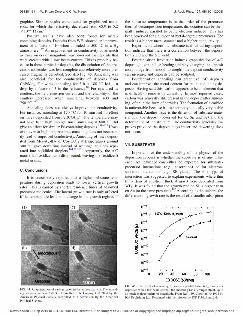
graphite. Similar results were found for graphitized nano-rods, for which the resistivity decreased from 68.9 to 5.2�10−4 cm.77
Positive results have also been found for metal-containing deposits. Deposits from WF6 showed an improve-ment of a factor of 10 when annealed at 500 °C in a H2
atmosphere.159 An improvement in conductivity of as muchas three orders of magnitude was observed for deposits thatwere created with a low beam current. This is probably be-cause in those particular deposits, the dissociation of the pre-cursor molecules was less complete and relatively more pre-cursor fragments desorbed. See also Fig. 45. Annealing wasalso beneficial for the conductivity of deposits fromCpPtMe3. For wires, annealing for 2 h at 180 °C led to adrop by a factor of 3 in the resistance.89 For tips used asemitters, the field emission current and the reliability of theemitters increased when annealing between 400 and750 °C.160
Annealing does not always improve the conductivity.For instance, annealing at 170 °C for 10 min had no effecton wires deposited from Fe3�CO�12.
91 The temperature maynot have been high enough since annealing at 600 °C didgive an effect for similar Fe-containing deposits.151–153 How-ever, even at high temperatures, annealing does not necessar-ily lead to improved conductivity. Annealing of lines depos-ited from Me2-Au-tfac or Co2�CO�8 at temperatures around300 °C gave dewetting instead of wetting: the lines sepa-rated into solidified droplets.104,121,161 Apparently, the a-Cmatrix had oxidized and disappeared, leaving the �oxidized�metal grains.
C. Conclusions
It is consistently reported that a higher substrate tem-perature during deposition leads to lower vertical growthrates. This is caused by shorter residence times of adsorbedprecursor molecules. The lateral growth rate is only affectedif the temperature leads to a change in the growth regime. If
the substrate temperature is in the order of the precursorthermal decomposition temperature, dissociation can be ther-mally induced parallel to being electron induced. This hasbeen observed for a number of metal-organic precursors. Theresult is a higher metal content and a higher conductivity.
Experiments where the substrate is tilted during deposi-tion indicate that there is a correlation between the deposi-tion yield and the SE yield.
Postdeposition irradiation induces graphitization of a-Cdeposits, it can induce heating �thereby changing the depositmorphology from smooth to rough�, the deposit conductivitycan increase, and deposits can be sculpted.
Postdeposition annealing can graphitize a-C depositsand can improve the metal content for metal-containing de-posits. Having said this, carbon appears to be an element thatis difficult to remove by annealing. In most reported cases,carbon was generally still present in the deposit after anneal-ing, often in the form of carbides. The formation of a carbideis unfavorable because it is a thermodynamically very stablecompound. Another issue is the diffusion of substrate mate-rial into the deposit �observed for C, Si, and Fe� and thedeformation of the structure. The conductivity generally im-proves provided the deposit stays intact and dewetting doesnot occur.
VII. SUBSTRATE
Important for the understanding of the physics of thedeposition process is whether the substrate is of any influ-ence. An influence can either be expected for substrate-precursor interactions �e.g., adsorption� or for electron-substrate interactions �e.g., SE yields�. The first type ofinteraction was suggested to explain experiments where thinfilms �tens of angstrom thick at most� were deposited fromWF6. It was found that the growth rate on Si is higher thanon Au �at the same pressure�.162 According to the authors, thedifference in growth rate is the result of a smaller adsorption
FIG. 44. Graphitization of carbon nanowire by an iron particle. The anneal-ing temperature was 650 °C. From Ref. 156. Copyright © 2004 by theAmerican Physical Society. Reprinted with permission by the AmericanPhysical Society.
FIG. 45. The effect of annealing of wires deposited from WF6. For wiresdeposited with a low beam current, the annealing has a stronger effect, up toas much as three orders of magnitude. From Ref. 159. Copyright © 1998 byIOP Publishing Ltd. Reprinted with permission by IOP Publishing Ltd.
081301-31 W. F. van Dorp and C. W. Hagen J. Appl. Phys. 104, 081301 �2008�
Downloaded 15 Sep 2010 to 131.180.130.114. Redistribution subject to AIP license or copyright; see http://jap.aip.org/about/rights_and_permissions

coefficient of WF6 on Au than on Si. This seems likely sincethe SE yield is in general larger for Au than for Si.163
However, in most other studies, deposits are thicker andthe relevant surface is the deposit surface, not the substratesurface. Therefore, in most cases, the electron-substrate in-teractions are dominant instead of the substrate-precursor in-teractions. The former become visible as differences in BSEand SE yields and in the spatial extent of the electron scat-tering in the substrate. Indications of the influence of BSEand SE yields come from experiments and simulations on,again, deposition on Au and Si. A Si sample was partiallycoated with a 500 nm layer of Au and deposition was per-formed over the edge of the Au layer with hfac-Cu-VTMS.The vertical growth rate was a factor of about 1.5 larger onthe Au than on the Si.86 This ratio compared well to calcu-lated BSE yields for the two situations. Unfortunately, thedeposition yields for a carbon precursor �acrylic acid� on thesame substrate agree less well with the simulated BSE andSE yields. The author tentatively suggested a slightly differ-ent dissociation process �radical or ion assisted� but still as-sumed that the model is correct.
As far as the vertical growth rate is concerned, onewould expect that the influence of the substrate is negligiblewhen depositing tips. For most of the time, the interactionstake place in the tip and not in the underlying substrate. Thistheory is confirmed by experiments where tips were depos-ited on Al, Ti, Cu, W, Mo, and Pb. There was no significanteffect of the substrate on the vertical growth rate, composi-tion, or morphology.86 Contradicting results were found forthe deposition of self-standing contamination rods. Differentgrowth rates were observed for various substrates �amongothers Al, Ti, Cu, and W�.164 However, since the residual gaswas used as precursor and cleaning procedures of the sub-strates were not described, the concentration of residual gasmolecules on the samples may not have been constant. Fur-thermore, one would expect substrate effects to be very smallbecause the majority of the relevant interactions occur on thegrowing self-standing rod, nearly completely away from thesubstrate.
Clearer examples of the influence of the substrate-electron interactions come from experiments where the de-posit width is studied. For instance, when depositing con-tamination lines on GaAs and Si, significant shoulders on thelines were observed.114 The width of the shoulders appears tobe dependent on the substrate. Region 1 in Fig. 46�a� is thearea where the PEs impinge on the GaAs substrate and re-gion 2 indicates the range over which BSEs and SEs “inter-act with the substrate surface.” They calculated the spatialextent of BSE scattering in the substrate for GaAs and Si andindicated this with the dashed lines in Figs. 46�a� and 46�b�,respectively. The calculated range is larger in Si than inGaAs, which is the result of the smaller density of Si. Thiscoincides “fairly well” with the extent of region 2 for bothsamples. Furthermore, the measured height in region 2 isalso less for Si than for GaAs, which is “consistent with theenergy of the e-beam being scattered over a larger volume inthe Si.” This is a similar effect to the BSE proximity effectdescribed in Sec. IVE1 �see also Fig. 33�b��. A similar de-pendency on the spatial distribution of electron scattering in
the substrate was found for the diameter of tips. The diam-eter of tips deposited from CpPtMe3 on Si, Cu, and SiOx
substrates were 199, 146, and 49 nm, respectively, at identi-cal accumulated charges.70 These diameters “correspondwith the main path length of those materials and the relatedproximity function.”
Regarding the influence of the thickness of the substrate,there seems to be no effect on the width of deposits. Dotswere deposited from W�CO�6 on areas that were transparent�thin� and nontransparent �thick� to 200 keV electrons of aSi�110� sample. The width of the dots was not significantlyinfluenced by substrate thickness.165 This was confirmed byMonte Carlo simulations.48,166
Apart from adsorption behavior or the spatial extent ofelectron scattering, the conductivity of the substrate is alsofound to be of influence on the deposition process. An ex-ample of this, the deformation proximity effect, was alreadydiscussed in Sec. V E 1. Depending on the conductivity ofthe substrate, already deposited structures were found to de-form when new structures were grown in the neighborhood�see Figs. 38�b� and 38�c��. Another example is the growth ofdendritic structures on insulating substrates such asAl2O3,167–170 BN,171 and tetragonal zirconia crystals.172 Thedimensions of the structures can vary by orders of magnitude�see Figs. 47�a� and 47�b�� and the formation was observedfor metal-organic precursors �e.g., W�CO�6� and contamina-tion. It is assumed that the dendritic growth is caused bycharging of the sample. As a result of the charging, a localelectric field is formed, which concentrates at convex areas.If the electric field is strong enough �estimated field strengthsin the order of 106–107 V m−1� precursor molecules in thegas phase are polarized and/or ionized and will follow deter-ministic instead of ballistic trajectories.171 Similar growthwas also observed for W�CO�6 on 10 nm thick Si3N4
membranes.173 Arrays of dots were deposited in the STEM
FIG. 46. Height profiles for line depositions on �a� GaAs and �b� Si. FromRef. 114.
081301-32 W. F. van Dorp and C. W. Hagen J. Appl. Phys. 104, 081301 �2008�
Downloaded 15 Sep 2010 to 131.180.130.114. Redistribution subject to AIP license or copyright; see http://jap.aip.org/about/rights_and_permissions

�Fig. 47�c��. When the sample was tilted, it became apparentthat some of the dots were considerably higher than the av-erage dots �Fig. 47�d��. These outliers also showed branchingin some cases. This, and the fact that the irregular growthwas not observed close to conducting areas on the substrate,is a strong indication that charging played a significant role.
In conclusion, the substrate can affect the vertical growthrate. This can be due to changes in the adsorption behavior�for deposits several angstrom thick� and/or changes in theBSE and SE yields. The width of the deposits is found to bedependent on the spatial extent of the electron scattering inthe substrate. The thickness of the substrate does not seem toaffect the width of deposits. On insulating substrates, den-dritic and irregular growth was observed, behavior that ismost likely due to charging effects.
VIII. PRECURSOR
A. Introduction
The precursor molecules contain the material to be de-posited and as such, it is a crucial factor in the depositionprocess. Many different precursors have been tried for EBID.Figure 48 shows that carbon precursors �residual gas, con-tamination in the electron optical system, or carbon precur-sors� are most widely studied. W�CO�6, Fe�CO�5, andMe3PtCp are the most popular metal-organic precursors andWF6 is the most frequently used inorganic precursor. Silvis-Cividjian and Hagen41 presented a fairly complete list of theprecursors used, together with references.
According to Hoffmann,174 a suitable and useful precur-sor has a number of requirements: it needs to be a volatilecompound at room temperature �either a gas, liquid, or
solid�, it needs to decompose to the desired “product” in afast, clean, and highly selective way �ideally without addi-tional reactant gas�, vacuum contamination �corrosion�should not occur, it needs to evaporate completely, fast, andwithout residue, it needs to be stable during storage and sup-ply, and it is preferably nontoxic and not expensive. On topof these requirements, we have to keep in mind that deposi-tion experiments usually take place in high vacuum condi-tions and not in ultrahigh vacuum conditions. This meansthat there is a background pressure of water or air in theorder of 10−6 mbar. Still we want to have pure deposits.
At the moment, none of the precursors used for EBIDreach the desired level of performance. Frequently usedstable compounds such as W�CO�6 or PtCpMe3 yield depos-its that contain typically about 10% metal. WF6, a stablecompound that yields a higher concentration of metal �80%–100%�, is an aggressive precursor that can damage electronoptical equipment.175 AuCl�PF�3 or D2GaN3, precursors thatare known to yield pure deposits and are not aggressive, arevery unstable and can be difficult or even dangerous to workwith.176 Moreover, a precursor such as AuCl3 does, in certainconditions, not yield any Au at all.177 It can be safely statedthat currently the main factor limiting the application ofbeam induced deposition in devices is the lack of controlover the composition of the deposits. Despite the importanceof a good understanding of the dissociation mechanism forthe progress in FEBIP research, the subject receives a rela-tively small amount attention compared to the other param-eters described in this review. Improvement is mainly triedthrough tweaking of the beam parameters �beam current, ac-celeration voltage� or postprocessing. The choice of precur-sor is mostly determined by the fact whether it is used oftenand whether it is readily available. Nearly all of the precur-sors used for deposition stem from the CVD world and therehas been hardly any search for precursors dedicated to FE-BIP.
B. Precursor gas only
In order to make a start with the understanding of thedissociation mechanisms of precursors, systematic studiesare required. There are a few such studies.
FIG. 47. Examples of the effect of an insulating substrate. �a� Dendriticgrowth from hydrocarbons on a BN crystal as result of broad beam illumi-nation. From Ref. 171. Copyright © 1995 by the American Physical Society.Reprinted with permission by the American Physical Society. �b� Dendriticgrowth from W�CO�6 on Al2O3 as a result of broad beam illumination. FromRef. 168. �c� An array of dots deposited from W�CO�6 on Si3N4. From Ref.173. Copyright © 2007 by IOP Publishing Ltd. Reprinted with permissionfrom IOP Publishing Ltd. �d� Same array as in �c� but now viewed under atilt angle of 20°. The outliers are clearly higher than the average deposit andalso show branching. From Ref. 173. Copyright © 2007 by IOP PublishingLtd. Reprinted with permission from IOP Publishing Ltd.
FIG. 48. Histogram of the number of articles that report on work on specificprecursors. The ten most popular precursors are shown.
081301-33 W. F. van Dorp and C. W. Hagen J. Appl. Phys. 104, 081301 �2008�
Downloaded 15 Sep 2010 to 131.180.130.114. Redistribution subject to AIP license or copyright; see http://jap.aip.org/about/rights_and_permissions

A study was made of the composition of deposits frompurely organic precursors �styrene, acrylic acid, propionicacid, acetic acid, and formic acid� and precursors containingfluorine, nitrogen, and chlorine �trifluoroacetic acid, acetoni-trile, and CCl4�. Analysis techniques used were energy dis-persive x-ray �EDX�, micro elastic recoil detection analysis�ERDA�, micro Fourier transform infrared spectroscopy�FTIR�, and micro-Raman. Surprisingly, the EDX,ERDA, and FTIR measurements show that the depositsfrom the purely organic precursors are all chemically verysimilar.86,178 The composition is C9H2O �regardless of thestoichiometric composition of the precursor� and 90%–95%of the carbon is sp2 bonded �C–C� and 5%–10% is sp3
bonded �C–H�. The micro-Raman measurements indicatethat the carbon deposits consist of nanocrystalline graphitewith cluster sizes around 2 nm. Similar results are found forthe precursors containing the components F, N, and Cl. Itwas found that 90% of these specific components are lostduring the deposition, either during precursor fixation or bycontinued irradiation of already deposited material during thedeposition process. Analysis of deposits from two paraffins�C22H46 and C24H50� with EELS and Raman confirm theseresults.16 Again, 80%–90% of the carbon atoms were sp2
bonded and Raman studies showed a similar amount of dis-order in the carbon.
Regarding the growth rate and the growth behavior, sig-nificant differences were found between acrylic acid and sty-rene. With a similar precursor flux reaching the irradiatedarea, acrylic acid has a five times higher growth rate thanstyrene.178 This is most likely due to the longer residencetimes of the acrylic acid molecules on the adsorption sites,which means that its sticking coefficient is higher. This iscaused by the fact that acrylic acid is a polar molecule andcan form H bonds, interactions that are much stronger thanthe van der Waals forces for styrene.
Another difference is the deposit smoothness. Whilemost of the precursors yield a smooth deposit, the depositsfrom formic acid are sometimes �and not reproducibly�rough and have a hollow structure178 �see Fig. 49�. Appar-ently, electron induced desorption of volatile elements occursinside the deposits after precursor fixation because thesevolatile elements are present in the precursor in a high ratiocompared to the carbon �C / �O+H�= 1
4�.
In another comparative study, the composition of depos-its from four Cu precursors was determined: Cu�hfac�2,hexafluoro-acetylacetonate copper dimethyl-1-hexen-3-yne�hfac-Cu-MHY�, hfac-Cu-VTMS, and hexafluoro-acetylacetonate copper dimethyl-butene �hfac-Cu-DMB�. ForCu�hfac�2 and hfac-Cu-MHY stable compositions of 13%–14% Cu and 75%–80% C were found during sputteringcycles.125 The Cu content for hfac-Cu-VTMS and hfac-Cu-DMB was estimated to be 15%–20% and 60%–70% C. Thefluorine signal was not above the noise level. The authorsconcluded that the Cu content is not determined by the stoi-chiometric composition of the precursors but more by thethermodynamic precursor stability and the electron/precursorflux ratio. These results are mostly consistent with experi-ments where the composition of physisorbed multilayers anddeposits from hfac-Cu-VTMS was studied. It was found thatthe electron bombardment mostly affects the fluorine- andoxygen-containing groups in the hfac ligands, while the CHx
groups from the VTMS and hfac ligands remain mostlyunaffected.52
Two Rh precursors, �RhCl�PF3�2�2 and �RhCl�CO2��2,appear to have decomposition paths very similar to eachother.108 The composition for both precursors was indepen-dent on the accumulated charge, which indicates that thedeposit is chemically quite stable. The Rh content was 60%and 56%, respectively, and the Cl content was 7% and 5%,respectively. The elements that are at the core of the precur-sor molecules are present in relatively high concentrations�19% P for the carbon-free precursor, 34% C for the carbon-containing precursor� and fluorine was not detected in eitherof the deposits. These experimental results are in contradic-tion with a theoretical model made for �RhCl�PF3�2�2. Cal-culations based on density functional theory on the lowestenergy pathways for decomposition indicate that the loss ofthe PF3 ligands is most favorable.179 However, the e-beaminduced deposits contain P and no F. Similar results wereobtained for Pt�PF3�4. It was found that electrons mainlyinduce scissions of the P–F bond and not the removal ofcomplete PF ligands as in the case for thermal decompositionin CVD. The discrepancy between results from EBID on theone hand and results from calculations and CVD on the othersuggests that the electron induced dissociation is more com-plex than just a simple single-step process.
FIG. 49. Hollow pear shaped deposits from formic acid. From Ref. 86. Reprinted with permission from author.
081301-34 W. F. van Dorp and C. W. Hagen J. Appl. Phys. 104, 081301 �2008�
Downloaded 15 Sep 2010 to 131.180.130.114. Redistribution subject to AIP license or copyright; see http://jap.aip.org/about/rights_and_permissions

Few differences were observed between deposits fromthree Au precursors: Me2-Au-acac, Me2-Au-tfac, andMe2-Au-hfac. For all precursors, the deposit composition is10% Au, 20% O, and 70% C for beam currents �900 pA.29
Again, fluorine is not detected. This indicates that the de-composition mechanism is similar.
For the cases described above, the dissociation was elec-tron induced. In some of the preceding sections, it has be-come clear that the contribution of thermal decomposition tothe growth can be significant. In general, this is beneficial forthe purity of the deposits, but in some cases the size and/orprecise location of the deposit is more difficult to control.This was, for instance, observed when creating deposits witha large accumulated charge �Co2CO8� �Ref. 87� with highbeam currents �Me2-Au-acac, Me2-Au-tfac, Me2-Au-hfac,Cu�hfac�2, Mo�CO�6, Me3PtCp, Co2CO8,87 Co�CO3�NO,8
hfac-Cu-VTMS �Ref. 86�� or in situations where the thermalconductivity of the deposit was low �hfac-Cu-VTMS�.115 In-dications of autocatalytic effects were found for Fe�CO�5.138
These thermal effects are clearly precursor dependent. As anexample, no thermal effects have been observed for�RhCl�PF3�2�2, even though different scan patterns and depo-sition conditions have been tried.179
Despite the indications that thermal effects are involved,it is not so easy to link the above-mentioned effects to thethermal decomposition temperature. The precursorsCo2�CO�8 and hfac-Cu-VTMS showed thermally enhanceddecomposition and have a low thermal decomposition tem-perature: 60 �Ref. 141� and 63 °C,125 respectively. Fe�CO�5
has demonstrated steady-state thermal decomposition even at−20 °C.139 For these precursors, thermally assisted decom-position has been observed during deposition. As mentioned,thermally assisted decomposition was not observed for�RhCl�PF3�2�2, which also has a much higher thermal de-composition temperature �160 °C�.180 So far the trend isconsistent, but this trend is contradicted by the thermal de-composition temperature of Co�CO3�NO and Me2-Au-hfac:162 �Ref. 181� and 160 °C,182 respectively.
Further evidence of the complexity of the dissociationprocess comes from studies on the proximity effects and thedeposition on insulators. From the discussion of the variousproximity effects in Sec. V E 2 it became apparent that thecomposition of parasitic deposits can be very different fromthe primary deposits. The composition of dendritic structurescreated on insulating substrates �discussed in Sec. VII� canalso be very different from the usual, nondendritic deposits.For instance, deposits created from W�CO�6 are usuallynanocomposites,128 with small W crystals in an a-C matrix.However, the dendritic structures obtained on insulating sur-faces were pure bcc tungsten crystals.167 In contrast, den-dritic structures created on insulators from the Pt precursorwere not pure Pt but nanocomposites.169
Such contradictions, together with the observations that�1� in some cases the stoichiometric composition of a precur-sor seems to be irrelevant for the deposit composition �forthe mentioned C, Cu, and Au precursors� and �2� that elec-tron induced dissociation does not necessarily follow eitherthe theoretically calculated lowest energy pathway or thethermal decomposition path, show that the dissociation
mechanism is not as simple as one may initially expect. Theresults also show that further detailed studies into the precur-sor chemistry and dissociation mechanisms are required tobe able to improve the deposit composition.
C. Reactive gases
Although the precursor chemistry is complex enoughwhen the precursor gas is the only gas, as became clear inSec. VIII B, it is possible to influence the decompositionmechanism by mixing in additional gases, so-called reactivegases. The idea is that the reactive gas forms volatile com-ponents with unwanted fragments that otherwise remain onthe sample after the dissociation of the precursor molecules.This prevents these fragments from polluting the deposit.Strictly speaking, nearly all experiments described in thisreview are done in the presence of a reactive gas. After all,the typical FEBIP system has a background vacuum of nobetter than 10−6 or 10−7 mbar, which is mostly due to thepresence of water and air. Depending on the cleanliness ofthe system, carbon contamination will also be present. There-fore, during a typical FEBIP experiment, precursor mol-ecules will be competing with, for instance, water moleculesfor surface adsorption sites and there will always be oxidiz-ing components available to react with dissociation frag-ments.
However, there are a number of reports where the pres-sure of reactive gases was raised significantly above thebackground level. In a relatively simple example of precur-sor chemistry, the effect of mixing H2 with WCl6 duringdeposition was tested.142 This made the W content increasefrom 95% to 100%, probably by the formation of HCl. Usinga more complicated combination, Folch et al.183 mixed 130mTorr of Me2-Au-hfac with 3 Torr of H2O and with a mix-ture of 2 Torr of O2 and 8 Torr of Ar. While the Au content ofsquares deposited without reactive gas was 2%–3% at most,this increased to 20% when H2O was added and increased toabout 50% when the Ar /O2 mixture was added. According tothe authors, H2O or O2 are ionized by the e-beam, react withthe C from the deposits, and form CO2 or CO. This wouldexplain that the Ar /O2 mixture has more effect than the H2Obecause there is more O present. Mølhave et al.15 performeda similar experiment. They used a similar precursor�Me2-Au-acac, partial pressure not reported�, mixed in 0.4–0.9 Torr H2O, and instead of depositing squares, they depos-ited tips and wires �see Fig. 50�. The results are quite differ-ent. The Au content increased but not homogeneouslydistributed over the deposits. The gold was concentratedmostly in the core of the tips and wires, surrounded by ashell of amorphous carbonaceous material. This particularcore-shell structure could only be fabricated in the presenceof water; mixtures of H2 and O2 with the same amount of Hand O as 0.8 Torr of H2O did not have such an effect. Thatthe effect of H2O on the deposit composition is far fromconsistent becomes evident from experiments by Tseng.184
Me3PtCp was mixed with H2O and no influence was foundon the deposit composition.
Wang et al.62 introduced O2 during deposition fromPt�PF3�4, but the Pt content increased only by a small
081301-35 W. F. van Dorp and C. W. Hagen J. Appl. Phys. 104, 081301 �2008�
Downloaded 15 Sep 2010 to 131.180.130.114. Redistribution subject to AIP license or copyright; see http://jap.aip.org/about/rights_and_permissions

amount, from around 17% to around 22%. Better resultswere obtained by Fischer et al.,105 who added oxygen duringthe deposition of SiO2 �precursor not mentioned� and wereable to create carbon-free deposits.
D. Precursor pressure
It is consistently reported that higher gas pressures leadto higher growth rates.25,60,143,185 In Fig. 51, the growth rateis plotted as a function of the current density for three dif-ferent Ru3�CO�12 fluxes: �1� 3 cm−2 s−1, �2� 1.5 cm−2 s−1,and �3� 0.9 cm−2 s−1. As the precursor flux increases, so doesthe growth rate. In the initial stages, the growth is e.l. In thefinal stages, the growth is p.l.
A simulation has been developed to determine the localdistribution of precursor molecules on the substrate for thesupply from a gas nozzle typically used in FEBIP experi-ments. In the Monte Carlo simulation, molecular flow con-ditions are assumed. The distribution from the model is com-pared to the height distribution of impinging precursormolecules that are thermally dissociated on a heated sub-strate. A good quantitative agreement is found �see Fig.51�b��.186
Some reports mention the existence of a minimum gaspressure required for deposition. A pressure threshold of8.6�10−4 Pa was found for deposition from CrO2Cl2.98Below this pressure, no Cr deposition was observed. It wasfound that etching of the �Cl-deficient� CrOxCly film oc-curred during postdeposition irradiation in the presence ofCl2. The authors suggested that there are two competing pro-cesses during growth from CrO2Cl2: dissociation of CrO2Cl2and recombination of CrOxCly with Cl. How the presence ofthese two competing processes would lead to the observedpressure threshold does not become quite clear. Pressurethresholds were also found for W�CO�6 �1�10−6 Pa� andMe2-Au-acac �5�10−7 Pa�.80 Growth was not observed be-low these thresholds regardless of the beam current. The au-thors suggested that a requirement for deposit growth is thepresence of stable nuclei on the substrate. Below the men-tioned precursor pressures, “the nuclei will not grow.” Thiswould indicate a nonlinearity of a type that has not yet beenreported elsewhere. Another explanation for the pressurethreshold could be again two competing processes: this time
dissociation of precursor molecules and knock-on damage bythe PEs. The PE energy was 200 keV and sputtering of thedeposit nuclei by the PEs is conceivable.49
Morphological changes were observed for deposits fromNi�C5H5�2 as a function of the gas pressure �in the range of10−6–10−8 mbar� and substrate temperature �in the range of−103 to –25 °C�. Depending on the precise conditions, uni-form �Figs. 52�a� and 52�b�� or open structures �Figs. 52�c�and 52�d�� were found.76 It appeared that the formation ofuniform or open structures was determined by the ratio be-tween the precursor partial pressure Ppartial and the precursorequilibrium pressure Pequilibrium at the corresponding sub-strate temperature. Uniform deposits were formed for ratiosPpartial / Pequilibrium�1 and open deposits were formed forPpartial / Pequilibrium�1. How these conditions lead to the ob-served morphologies was not explained.
E. Conclusions
From the few systematic studies that have been per-formed, it becomes clear that electron induced decomposi-tion is a complex process. It is consistently reported that thedeposit composition is not directly dependent on the stoichi-
FIG. 50. Core-shell structure for a tip deposited from Me2-Au-acac in thepresence of H2O. From Ref. 15. Copyright © 2003 by the American Chemi-cal Society. Reprinted with permission by the American Chemical Society.
FIG. 51. �a� Growth rate as a function of the current density for threedifferent Ru3�CO�12 fluxes. Precursor flux: �1� 3 cm−2 s−1, �2� 1.5 cm−2 s−1,and �3� 0.9 cm−2 s−1. From Ref. 60. Copyright © 1986 by Elsevier. Re-printed with permission by Elsevier. �b� Comparison of the impinging pre-cursor distribution between experiment �gray scale height map� and simula-tion �isodensity contours�. From Ref. 186. Copyright © 2006 by Elsevier.Reprinted with permission by Elsevier.
081301-36 W. F. van Dorp and C. W. Hagen J. Appl. Phys. 104, 081301 �2008�
Downloaded 15 Sep 2010 to 131.180.130.114. Redistribution subject to AIP license or copyright; see http://jap.aip.org/about/rights_and_permissions
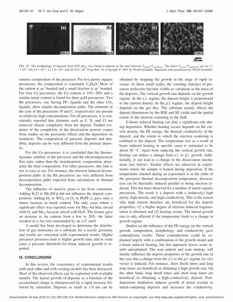
ometric composition of the precursor. For five purely organicprecursors, the composition is constantly C9H2O. Most ofthe carbon is sp2 bonded and a small fraction is sp3 bonded.For four Cu precursors, the Cu content is 10%–20% and asimilar metal content is found for three gold precursors. TwoRh precursors, one having PF3 ligands and the other CO2
ligands, show similar decomposition paths. The elements atthe core of the precursors �P and C, respectively� are presentin relatively high concentrations. For all precursors, it is con-sistently reported that elements such as F, N, and Cl areremoved almost completely from the deposit. Further evi-dence of the complexity of the dissociation process comesfrom studies on the proximity effects and the deposition oninsulators. The composition of parasitic deposits and den-dritic deposits can be very different from the primary depos-its.
For the Cu precursors, it is concluded that the thermo-dynamic stability of the precursor and the electron/precursorflux ratio, rather than the stoichiometric composition, deter-mine the final composition. For other precursors, this link isnot so easy to see. For instance, the electron induced decom-position paths of the Rh precursors are very different fromdecomposition paths expected from calculations or thermaldecomposition.
The influence of reactive gases is far from consistent.Adding H2O to Me3PtCp did not influence the deposit com-position. Adding H2 to WCl6 or O2 to Pt�PF3�4 gave only aminor increase in metal content. The only cases where asignificant effect was reported were for Me2-Au-hfac mixedwith O2 and Me2-Au-acac mixed with H2O. The former gavean increase in Au content from a few to 20%; the latterresulted in a Au core surrounded by an a-C shell.
A model has been developed to determine the distribu-tion of gas molecules on a substrate for a nozzle geometryand results are consistent with experimental results. Higherprecursor pressures lead to higher growth rates and in somecases a pressure threshold for beam induced growth is re-ported.
IX. CONCLUSIONS
In this review, the consistency of experimental resultswith each other and with existing models has been discussed.Most of the observed effects can be explained with availablemodels. The lateral growth of deposits as a function of theaccumulated charge is characterized by a rapid increase fol-lowed by saturation. Deposits as small as 1.0 nm can be
obtained by stopping the growth in the stage of rapid in-crease. At these small scales, the counting statistics of pre-cursor molecules become visible as variations in the mass ofthe deposits. The vertical growth rate depends on the growthregime. In the e.l. regime, the deposit height is proportionalto the current density. In the p.l. regime, the deposit heightdepends on the gas flux. The substrate mainly affects thedeposit dimensions by the BSE and SE yields and the spatialextent of the electron scattering in the bulk.
E-beam induced heating can play a significant role dur-ing deposition. Whether heating occurs depends on the cur-rent density, the PE energy, the thermal conductivity of thedeposit, and the extent to which the electron scattering isconfined to the deposit. The temperature rise as a result ofbeam induced heating in specific cases is estimated to beabout 50 °C. Apart from reducing the vertical growth rate,heating can induce a change from e.l. to p.l. growth. Addi-tionally, it can lead to a change in the dissociation mecha-nism �see below�. Similar effects are observed in experi-ments where the sample is heated during deposition. If thetemperature reached during an experiment is in the order ofthe precursor thermal decomposition temperature, dissocia-tion can be thermally induced parallel to being electron in-duced. This has been observed for a number of metal-organicprecursors. The result is a deposit with a �relatively� highpurity, high density, and high conductivity. This is the reasonwhy high current densities are beneficial for the depositproperties; �1� a higher degree of electron induced fragmen-tation is obtained and �2� heating occurs. The lateral growthrate is only affected if the temperature leads to a change ingrowth regime.
Studies on the influence of the PE energy on the verticalgrowth, composition, morphology, and conductivity gavecontradictory results. These contradictions could be ex-plained largely with a combination of the growth model ande-beam induced heating, but this approach leaves some re-sults unexplained. The scan pattern and scan strategy willmainly influence the deposit properties or the growth rate inthe case that a change from the e.l. to the p.l. regime �or viceversa� is induced. For instance, short dwell times and longloop times are beneficial in obtaining a high growth rate. Onthe other hand, long dwell times and short loop times arebeneficial in obtaining a high-conductivity deposit. Post-deposition irradiation induces growth of metal crystals inmetal-containing deposits and increases the conductivity.
FIG. 52. The morphology of deposits from Ni�C5H5�2 was found to depend on the ratio between Ppartial / Pequilibrium. The ratios Ppartial / Pequilibrium are �a� 1.7�10−4, �b� 6.5�10−4, �c� 1.8�101, and �d� 9.6�102. From Ref. 76. Copyright © 2001 by World Scientific. Reprinted with permission by World Scientific.
081301-37 W. F. van Dorp and C. W. Hagen J. Appl. Phys. 104, 081301 �2008�
Downloaded 15 Sep 2010 to 131.180.130.114. Redistribution subject to AIP license or copyright; see http://jap.aip.org/about/rights_and_permissions
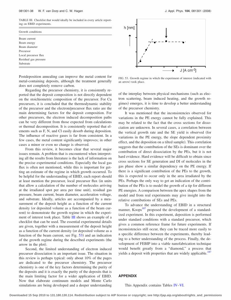
Postdeposition annealing can improve the metal content formetal-containing deposits, although the treatment generallydoes not completely remove carbon.
Regarding the precursor chemistry, it is consistently re-ported that the deposit composition is not directly dependenton the stoichiometric composition of the precursor. For Cuprecursors, it is concluded that the thermodynamic stabilityof the precursor and the electron/precursor flux ratio are themain determining factors for the deposit composition. Forother precursors, the electron induced decomposition pathscan be very different from those expected from calculationsor thermal decomposition. It is consistently reported that el-ements such as F, N, and Cl easily desorb during deposition.The influence of reactive gases is far from consistent. In afew cases, the metal content significantly improves; in othercases a minor or even no change is observed.
From this review, it becomes clear that several majorissues remain. A problem that is encountered when interpret-ing all the results from literature is the lack of information onthe precise experimental conditions. Especially the local gasflux is often not mentioned, while this is important for get-ting an estimate of the regime in which growth occurred. Tobe helpful for the understanding of EBID, each report shouldat least mention the precursor, local precursor flux �in unitsthat allow a calculation of the number of molecules arrivingat the irradiated spot per area per time unit�, residual gaspressure, beam current, beam diameter, acceleration voltage,and substrate. Ideally, articles are accompanied by a mea-surement of the deposit height as a function of the currentdensity �or deposited volume as a function of the beam cur-rent� to demonstrate the growth regime in which the experi-ment of interest took place. Table III shows an example of achecklist that can be used. The essential experimental detailsare given, together with a measurement of the deposit heightas a function of the current density �or deposited volume as afunction of the beam current, see Fig. 53� and an indicationof the growth regime during the described experiments �thearrow in the plot�.
Second, the limited understanding of electron inducedprecursor dissociation is an important issue. The situation inthis review is perhaps typical: only about 10% of the pagesare dedicated to the precursor chemistry. The precursorchemistry is one of the key factors determining the purity ofthe deposits and it is exactly the purity of the deposits that isthe main limiting factor for a wider application of EBID.Now that elaborate continuum models and Monte Carlosimulations are being developed and a deeper understanding
of the interplay between physical mechanisms �such as elec-tron scattering, beam induced heating, and the growth re-gimes� emerges, it is time to develop a better understandingof the precursor chemistry.
It was mentioned that the inconsistencies observed forvariations in the PE energy cannot be fully explained. Thismay be related to the fact that the cross sections for disso-ciation are unknown. In several cases, a correlation betweenthe vertical growth rate and the SE yield is observed �forvariations in the PE energy, the slope dependent proximityeffect, and the deposition on a tilted sample�. This correlationsuggests that the contribution of the SEs is dominant over thecontribution of direct dissociation by the PEs, but it is nothard evidence. Hard evidence will be difficult to obtain sincecross sections for SE generation and DI of molecules in thegas phase show a similar dependency on the PE energy. Ifthere is a significant contribution of the PEs to the growth,this is expected to occur only in the area irradiated by thePEs. Perhaps the only way to get an indication of the contri-bution of the PEs is to model the growth of a tip for differentPE energies. A comparison between the apex shapes from themodel and from real experiments may give insight into therelative contributions of SEs and PEs.
To advance the understanding of EBID in a structuralmanner, Koops187 proposed the development of a standard-ized experiment. In this experiment, deposition is performedunder standard conditions with a standard precursor, whichgives a common reference frame for future experiments. Ifinconsistencies still occur, they can be traced more easily toa specific difference between the experiments, thereby lead-ing to a better understanding of the process. Finally, the de-velopment of FEBIP into a viable nanofabrication techniquewould benefit greatly from a “diamond,” a process thatyields a deposit with properties that are widely applicable.187
APPENDIX
This Appendix contains Tables IV–VI.
TABLE III. Checklist that would ideally be included in every article report-ing on EBID experiments.
Growth conditions
Beam currentBeam energyBeam diameterPrecursorLocal precursor fluxResidual gas pressureSubstrate
FIG. 53. Growth regime in which the experiment of interest �indicated withan arrow� took place.
081301-38 W. F. van Dorp and C. W. Hagen J. Appl. Phys. 104, 081301 �2008�
Downloaded 15 Sep 2010 to 131.180.130.114. Redistribution subject to AIP license or copyright; see http://jap.aip.org/about/rights_and_permissions

TABLE V. Symbols used.
Symbol Unit Meaning
Abeam �cm2� Area of the e-beamAdeposit �cm2� Area of the depositdbeam �cm� Diameter of the e-beamddeposit �cm� Diameter of the depositEdes �J� Desorption energyF �cm−2 s−1� Precursor gas fluxg Sticking factorh �nm� Deposit heightI �electrons s−1� CurrentJ �electrons s−1 cm−2� Total current densityJBSE �electrons s−1 cm−2� BSE current densityJPE �electrons s−1 cm−2� PE current densityJSE �electrons s−1 cm−2� SE current densityk �m2 kg s−2 K−1� Boltzmann constant
� �s−1�Vibrational frequencyof an adsorbed molecule
N �cm−2� Precursor molecule coverage
N0 �cm−2�Available adsorption sitesin a monolayer
Ppartial Pa Precursor partial pressurePequilibrium Pa Precursor equilibrium pressureQ �C� Accumulated chargeR �cm/s� Vertical growth rate��E� �cm2� Cross section for dissociation� �cm2� Integral value of ��E�
t �s� Timetdwell �s� Dwell time� �s� Residence timeT �K� TemperatureVdeposit �cm3� Volume of a depositVmolecule �cm3� Volume of a deposited molecule
TABLE VI. Abbreviations.
Abbreviation Short for
a-C Amorphous carbonBSE Backscattered electronDEA Dissociative electron attachmentDD Dipolar dissociationDI Dissociative ionizationFEBIP E-beam induced processingEELS Electron energy loss spectrometrye.l. Electron limitedFSE Forward scattered electronPE Primary electronp.l. Precursor limitedSE Secondary electronSEM Scanning electron microscopeSTEM Scanning transmission electron microscopeTEM Transmission electron microscopeUHV Ultrahigh vacuumUV Ultraviolet
TABLE IV. Precursor names.
Material Precursor Full name
Al TMA Tri-methyl-aluminum
Au AuCl�PF�3
Chloro�trifluorophosphine�gold
Au AuCl3 Gold trichloride
Au Me2-Au-acac Dimethyl acetylacetonate gold
Au Me2-Au-tfacDimethyl-trifluoro-acetylacetonate gold
Au Me2-Au-hfacDimethyl-hexafluoro-acetylacetonate gold
C C6H5CHCH2 Styrene
C CH2CHCOOH Acrylic acid
C CH3CH2COOH Propionic acid
C HCOOH Formic acid
C CH3COOH Acetic acid
C CH3C10H8 Alkylnaphthalene
Co Co2CO8
Dicobaltoctacarbonyl
Co �Co�CO3�NO� Cobalt tricarbonyl nitrosyl
Cu Cu�hfac�2
Bis-hexafluoro-acetylacetonate copper
Cu hfac-Cu-VTMS
Hexafluoro-acetylacetonatecopper vinyl-trimethyl-silane
Cu hfac-Cu-DMBHexafluoro-acetylacetonatecopper dimethyl-butene
Cu hfac-Cu-MHY
Hexafluoro-acetylacetonatecopper dimethyl-1-hexen-3-yne
Cr CrO2Cl2 Chromyl chloride
Cr Cr�CO�6 Chromium hexacarbonyl
Fe Fe�CO�5 Iron pentacarbonyl
Fe Fe3�CO�12 Tri-iron dodecacarbonyl
GaAs TMG and AsH3
Tri-methyl-galliumand arsine
GaN D2GaN3
Perdeuteratedgallium azide
Ir �IrCl�PF3�2�2
Di--chloro-tetrakistrifluorophosphine di-iridium
Mo Mo�CO�6 Molybdenum hexacarbonyl
Ni Ni�C5H5�2 Nickelocene
Os Os3�CO�12 Tri-osmium dodecacarbonyl
Pt CpPtMe3
Trimethyl-platinum-cyclopentadienyl
Pt MeCpPtMe3
Trimethyl-platinum-methylcyclopentadienyl
Pt Pt�PF3�4
Tetrakis trifluorophosphineplatinum
Re Re2�CO�10 Dirhenium decacarbonyl
Rh �RhCl�PF3�2�2
Di--chloro-tetrakistrifluorophosphine dirhodium
Rh �RhCl�CO�2�2
Tetracarbonyl di-�-chloro dirhodium
Ru Ru3�CO�12 Triruthenium dodecacarbonyl
Si SiH2Cl2 Dichlorosilane
SiOx TEOS Tetra-ethoxy-silane
SiOx TMOS Tetramethyl ortho-silicate
W W�CO�6 Tungsten hexacarbonyl
W WF6 Tungsten hexafluoride
W WCl6 Tungsten hexachloride
081301-39 W. F. van Dorp and C. W. Hagen J. Appl. Phys. 104, 081301 �2008�
Downloaded 15 Sep 2010 to 131.180.130.114. Redistribution subject to AIP license or copyright; see http://jap.aip.org/about/rights_and_permissions

1R. L. Stewart, Phys. Rev. 45, 488 �1934�.2R. W. Christy, J. Appl. Phys. 31, 1680 �1960�.3A. G. Baker and W. C. Morris, Rev. Sci. Instrum. 32, 458 �1961�.4B. Hübner and H. W. P. Koops, Ultramicroscopy 42-44, 1519 �1992�.5C. Schoessler and H. W. P. Koops, J. Vac. Sci. Technol. B 16, 862 �1998�.6I. Utke, P. Hoffmann, R. Berger, and L. Scandella, Appl. Phys. Lett. 80,4792 �2002�.
7I. Utke, T. Bret, D. Laub, Ph. Buffat, L. Scandella, and P. Hoffmann,Microelectron. Eng. 73-74, 553 �2004�.
8Y. M. Lau, P. C. Chee, J. T. L. Thong, and V. Ng, J. Vac. Sci. Technol. A20, 1295 �2002�.
9K. I. Schiffmann, Nanotechnology 4, 163 �1993�.10M. Wendel, H. Lorenz, and J. P. Kotthaus, Appl. Phys. Lett. 67, 3732
�1995�.11C. Schössler, J. Urban, and H. W. P. Koops, J. Vac. Sci. Technol. B 15,
1535 �1997�.12K. Edinger, T. Gotszalk, and I. W. Rangelow, J. Vac. Sci. Technol. B 19,
2856 �2001�.13J. H. Kindt, G. E. Fantner, J. B. Thompson, and P. K. Hansma, Nanotech-
nology 15, 1131 �2004�.14P. Bøggild, T. M. Hansen, O. Kuhn, F. Grey, T. Junno, and L. Montelius,
Rev. Sci. Instrum. 71, 2781 �2000�.15K. Mølhave, D. Nørgaard Madsen, A. M. Rasmussen, A. Carlsson, C. C.
Appel, M. Brorson, C. J. H. Jacobsen, and P. Bøggild, Nano Lett. 3, 1499�2003�.
16W. Ding, D. A. Dikin, X. Chen, R. D. Piner, R. S. Ruoff, E. Zussman, X.Wang, and X. Li, J. Appl. Phys. 98, 014905 �2005�.
17M. F. Yu, O. Lourie, M. J. Dyer, K. Moloni, T. F. Kelly, and R. S. Ruoff,Science 287, 637 �2000�.
18T. Fukuda, F. Arai, L. Dong, and M. Nakajima, Fifth World Congress onIntelligent Control and Automation 701, 2698 �2004�.
19T. Brintlinger, M. S. Fuhrer, J. Melngailis, I. Utke, T. Bret, A. Perentes, P.Hoffmann, M. Aboudira, and P. Doppelt, J. Vac. Sci. Technol. B 23, 3174�2005�.
20F. Banhart, Nano Lett. 1, 329 �2001�.21P. G. Li, A. Z. Jin, and W. H. Tang, Phys. Status Solidi A 203, 282 �2006�.22M. D. Croitoru, G. Bertsche, D. R. Kern, C. Burkhardt, S. Bauerdick, S.
Şahakalkan, and S. Roth, J. Vac. Sci. Technol. B 23, 2789 �2005�.23Y. Tsukatani, N. Yamasaki, K. Murakami, F. Wakaya, and M. Takai, Jpn. J.
Appl. Phys., Part 1 44, 5683 �2005�.24L. Rotkina, J. F. Lin, and J. P. Bird, Appl. Phys. Lett. 83, 4426 �2003�.25H. W. P. Koops, R. Weiel, D. P. Kern, and T. H. Baum, J. Vac. Sci.
Technol. B 6, 477 �1988�.26K. Edinger, H. Becht, J. Bihr, V. Boegli, M. Budach, T. Hofmann, H. W.
P. Koops, P. Kuschnerus, J. Oster, P. Spies, and B. Weyrauch, J. Vac. Sci.Technol. B 22, 2902 �2004�.
27T. Liang, E. Frendberg, B. Lieberman, and A. Stivers, J. Vac. Sci. Technol.B 23, 3101 �2005�.
28K. Murakami and M. Takai, J. Vac. Sci. Technol. B 22, 1266 �2004�.29M. Weber, M. Rudolph, J. Kretz, and K. W. P. Koops, J. Vac. Sci. Technol.
B 13, 461 �1995�.30C. J. Edgcombe and U. Valdre, Philos. Mag. B 82, 987 �2002�.31G. Boero, I. Utke, T. Bret, N. Quack, M. Todorova, S. Mouaziz, P. Keijk,
J. Brugger, R. S. Popovic, and P. Hoffmann, Appl. Phys. Lett. 86, 042503�2005�.
32C. P. Umbach, S. Washburn, R. A. Webb, R. Koch, M. Bucci, A. N.Broers, and R. B. Laibowitz, J. Vac. Sci. Technol. B 4, 383 �1986�.
33P. Bøggild, T. M. Hansen, C. Tanasa, and F. Grey, Nanotechnology 12,331 �2001�.
34T. Ooi, K. Matsumoto, M. Nakao, M. Otsubo, S. Shirakata, S. Tanaka, andY. Hatamura, Proceedings of the IEEE Micro Electro Mechanical Systems�MEMS�, 2000 �unpublished�, p. 580.
35A. Perentes, A. Bachmann, M. Leutenegger, I. Utke, C. Sandu, and P.Hoffmann, Microelectron. Eng. 73–74, 412 �2004�.
36H. W. P. Koops, O. E. Hoinkis, M. E. W. Honsberg, R. Schmidt, B. Blum,G. Boettger, A. Kuligk, C. Liguda, and M. Eich, Microelectron. Eng.57–58, 995 �2001�.
37H. W. P. Koops, E. Munro, J. Rouse, J. Kretz, M. Rudolph, M. Weber, andG. Dahm, Nucl. Instrum. Methods Phys. Res. A 363, 1 �1995�.
38N. Miura, H. Ishii, J. Shirakashi, A. Yamada, and M. Konagai, Appl. Surf.Sci. 113-114, 269 �1997�.
39T. Mukawa, S. Okada, R. Kobayashi, J. Fujita, M. Ishida, T. Ichihashi, Y.Ochiai, T. Kaito, and S. Matsui, Jpn. J. Appl. Phys., Part 1 44, 5639�2005�.
40S. J. Randolph, J. D. Fowlkes, and P. D. Rack, J. Appl. Phys. 97, 124312�2005�.
41N. Silvis-Cividjian and C. W. Hagen, Adv. Imaging Electron Phys. 143, 1�2006�.
42S. J. Randolph, J. D. Fowlkes, and P. D. Rack, Crit. Rev. Solid StateMater. Sci. 31, 55 �2006�.
43L. Reimer, Scanning Electron Microscopy �Springer-Verlag, Berlin, 1998�.44N. Silvis-Cividjian, “Electron Beam Induced Nanometer Scale Deposi-
tion,” Ph.D. thesis, Delft University, 2002.45T. Koshikawa and R. Shimizu, J. Phys. D 7, 1303 �1974�.46M. Kotera, J. Appl. Phys. 65, 3991 �1989�.47D. C. Joy, Monte Carlo Modeling for Electron Microscopy and Mi-
croanalysis �Oxford University Press, New York, 1995�, and referencestherein.
48C. W. Hagen, N. Silvis-Cividjian, and P. Kruit, Scanning 27, 90 �2005�.49R. F. Egerton, F. Wang, and P. A. Crozier, Microsc. Microanal. 12, 65
�2006�.50P. Rowntree, L. Parenteau, and L. Sanche, J. Phys. Chem. 95, 4902 �1991�.51E. H. Hirsch, Br. J. Appl. Phys. 11, 547 �1960�.52S. Mezhenny, I. Lyubinetsky, W. J. Choyke, and J. T. Yates, J. Appl. Phys.
85, 3368 �1999�.53P. M. George and J. L. Beauchamp, Thin Solid Films 67, L25 �1980�.54P. Rowntree, Chemical Processes of Electron Beam Induced Deposition,
Presented at the First International EBID Workshop, Delft, 2006 �unpub-lished�.
55M. A. Henderson, R. D. Ramsier, and J. T. Yates, Surf. Sci. 259, 173�1991�.
56N. Silvis-Cividjian, C. W. Hagen, L. H. A. Leunissen, and P. Kruit, Mi-croelectron. Eng. 61–62, 693 �2002�.
57J. D. Fowlkes, S. J. Randolph, and P. D. Rack, J. Vac. Sci. Technol. B 23,2825 �2005�.
58K. Mitsuishi, Z. Q. Liu, M. Shimojo, M. Han, and K. Furuya, Ultrami-croscopy 103, 17 �2005�.
59C. Tian and C. R. Vidal, J. Phys. B 31, 895 �1998�.60V. Scheuer, H. W. P. Koops, and T. Tschudi, Microelectron. Eng. 5, 423
�1986�.61T. Ichihashi and S. Matsui, J. Vac. Sci. Technol. B 6, 1869 �1988�.62S. Wang, Y. M. Sun, Q. Wang, and J. M. White, J. Vac. Sci. Technol. B 22,
1803 �2004�.63W. Li and D. C. Joy, J. Vac. Sci. Technol. A 24, 431 �2006�.64A. Folch and J. Servat, J. Vac. Sci. Technol. B 14, 2609 �1996�.65T. Bret, I. Utke, P. Hoffmann, M. Aboudira, and P. Doppelt, Microelec-
tron. Eng. 83, 1482 �2006�.66I. Utke, V. Friedli, J. Michler, T. Bret, X. Multone, and P. Hoffmann, Appl.
Phys. Lett. 88, 031906 �2006�.67H. W. P. Koops, J. Kretz, and M. Rudolph, J. Vac. Sci. Technol. B 11, 2386
�1993�.68K. T. Kohlmann-von Platen, J. Chlebek, M. Weiss, and K. Reimer, J. Vac.
Sci. Technol. B 11, 2219 �1993�.69Z. Q. Liu, K. Mitsuishi, and K. Furuya, J. Appl. Phys. 96, 3983 �2004�.70U. Hübner, R. Plontke, M. Blume, A. Reinhardt, and H. W. P. Koops,
Microelectron. Eng. 57–58, 953 �2001�.71H. Hiroshima and M. Komuro, Nanotechnology 9, 108 �1998�.72D. Beaulieu, Y. Ding, Z. L. Wang, and W. J. Lakey, J. Vac. Sci. Technol.
B 23, 2151 �2005�.73P. Hoyle, J. Cleaver, and H. Ahmed, J. Vac. Sci. Technol. B 14, 662
�1996�.74M. Shimojo, W. Zhang, M. Takeguchi, M. Tanaka, K. Mitsuishi, and K.
Furuya, Jpn. J. Appl. Phys., Part 1 44, 5651 �2005�.75A. N. Broers, W. W. Molzen, J. J. Cuomo, and N. D. Wittels, Appl. Phys.
Lett. 29, 596 �1976�.76H. Jiang, C. N. Borca, B. Xu, and B. W. Robertson, Int. J. Mod. Phys. B
15, 3207 �2001�.77J. Fujita, M. Ishida, T. Ichihashi, Y. Ochiai, T. Kaito, and S. Matsui, J. Vac.
Sci. Technol. B 21, 2990 �2003�.78P. A. Crozier, J. Tolle, J. Kouvetakis, and C. Ritter, Appl. Phys. Lett. 84,
3441 �2004�.79O. Guise, J. Ahner, J. Yates, and J. Levy, Appl. Phys. Lett. 85, 2352
�2004�.80M. Tanaka, M. Shimojo, M. Han, K. Mitsuishi, and K. Furuya, Surf.
Interface Anal. 37, 261 �2005�.81W. F. Van Dorp, B. Van Someren, C. W. Hagen, P. Kruit, and P. A. Crozier,
Nano Lett. 5, 1303 �2005�.82W. F. Van Dorp, B. Van Someren, C. W. Hagen, P. A. Crozier, and P. Kruit,
081301-40 W. F. van Dorp and C. W. Hagen J. Appl. Phys. 104, 081301 �2008�
Downloaded 15 Sep 2010 to 131.180.130.114. Redistribution subject to AIP license or copyright; see http://jap.aip.org/about/rights_and_permissions
Microelectron. Eng. 83, 1468 �2006�.83H. W. P. Koops, J. Kretz, M. Rudolph, M. Weber, G. Dahm, and K. L. Lee,
Jpn. J. Appl. Phys., Part 1 33, 7099 �1994�.84H. W. P. Koops, A. Kaya, and M. Weber, J. Vac. Sci. Technol. B 13, 2400
�1995�.85M. Weber, H. W. P. Koops, M. R. Rudolph, J. Kretz, and G. Schmidt, J.
Vac. Sci. Technol. B 13, 1364 �1995�.86T. Bret, “Physico-chemical study of the focused electron beam induced
deposition process,” Ph.D. thesis, Ecole Polytechnique Fédérale de Lau-sanne, 2005.
87I. Utke, J. Michler, P. Gasser, C. Santschi, D. Laub, M. Cantoni, P. A.Buffat, C. Jiao, and P. Hoffmann, Adv. Eng. Mater. 7, 323 �2005�.
88R. R. Kunz and T. M. Mayer, J. Vac. Sci. Technol. B 6, 1557 �1988�.89C. Schößler, A. Kaya, J. Kretz, and H. W. P. Koops, Microelectron. Eng.
30, 471 �1996�.90K. T. Kohlmann-von Platen, L.-M. Buchman, H.-C. Petzold, and W. H.
Brünger, J. Vac. Sci. Technol. B 10, 2690 �1992�.91M. A. Bruk, E. N. Zhikharev, E. I. Grigor’ev, A. V. Spirin, V. A. Kal’nov,
and I. E. Kardash, High Energy Chem. 39, 65 �2005�.92I. Utke, P. Hoffmann, B. Dwir, K. Leifer, E. Kapon, and P. Doppelt, J. Vac.
Sci. Technol. B 18, 3168 �2000�.93M. Komuro and H. Hiroshima, Microelectron. Eng. 35, 273 �1997�.94H. Seiler, J. Appl. Phys. 54, R1 �1983�.95B. Völkel, A. Gölzhäuser, H. U. Müller, C. David, and M. Grunze, J. Vac.
Sci. Technol. B 15, 2877 �1997�.96S. Lipp et al., S. Bauerdick et al., D. Beaulieu et al., M. D. Croitoru et al.,
and K. T. Kohlmann-von Platen et al. report a change in beam currentwhen changing the PE energy; P.Hoyle et al., K. T. Kohlmann-von Platenet al., S. J. Randolph et al., K. I. Schiffmann et al., and N. Miura et al.have performed their experiments at a constant beam current, but reporteda change in the beam diameter when varying the PE energy.
97T. Bret, I. Utke, A. Bachmann, and P. Hoffmann, Appl. Phys. Lett. 83,4005 �2003�.
98S. Wang, Y. M. Sun, and J. M. White, Appl. Surf. Sci. 249, 110 �2005�.99P. Hoyle, J. Cleaver, and H. Ahmed, Appl. Phys. Lett. 64, 1448 �1994�.100M. Takai, W. Jarupoonphol, C. Ochiai, O. Yavas, and Y. K. Park, Appl.
Phys. A: Mater. Sci. Process. 76, 1007 �2003�.101S. Bauerdick, C. Burkhardt, R. Rudorf, W. Barth, V. Bucher, and W.
Nisch, Microelectron. Eng. 67–68, 963 �2003�.102S. Lipp, L. Frey, C. Lehrer, E. Demm, S. Pauthner, and H. Ryssel, Mi-
croelectron. Reliab. 36, 1779 �1996�.103D. Kunze, O. Peters, and G. Sauerbrey, Z. Angew. Phys. 22, 69 �1967�.104K. L. Lee and M. Hatzakis, J. Vac. Sci. Technol. B 7, 1941 �1989�.105M. Fischer, H. D. Wanzenboeck, J. Gottsbachner, S. Mueller, W. Brezna,
M. Schramboeck, and E. Bertagnolli, Microelectron. Eng. 83, 784 �2006�.106N. Miura, H. Ishii, A. Yamada, and M. Konagai, Jpn. J. Appl. Phys., Part
2 35, L1089 �1996�.107D. A. Bell, J. L. Falconer, Z. Lü, and C. M. McConica, J. Vac. Sci.
Technol. B 12, 2976 �1994�.108F. Cicoira, P. Hoffmann, C. O. A. Olsson, N. Xanthopoulos, H. J.
Mathieu, and P. Doppelt, Appl. Surf. Sci. 242, 107 �2005�.109V. Gopal, E. A. Stach, V. R. Radmilovic, and I. A. Mowat, Appl. Phys.
Lett. 85, 49 �2004�.110 J. Fourie, Optik �Jena� 44, 111 �1975�.111 L. Reimer and M. Wächter, Ultramicroscopy 3, 169 �1978�.112 I. Utke, V. Friedli, and J. Michler, “Resolution and Growth Regimes in
Focused Ion and Electron Beam Induced Processing,” J. Vac. Sci. Tech-nol. B �submitted�.
113 D. A. Smith, J. D. Fowlkes, and P. D. Rack, Nanotechnology 18, 265308�2007�.
114 M. Amman, J. Sleight, D. Lombardi, R. Welser, and M. Deshpande, J.Vac. Sci. Technol. B 14, 54 �1996�.
115 I. Utke, A. Luisier, P. Hoffmann, D. Laub, and P. A. Buffat, Appl. Phys.Lett. 81, 3245 �2002�.
116 Z. Q. Liu, K. Mitsuishi, and K. Furuya, Appl. Phys. A: Mater. Sci. Pro-cess. 80, 1437 �2005�.
117 F. Cicoira, K. Leifer, P. Hoffmann, I. Utke, B. Dwir, D. Laub, P. A.Buffat, E. Kapon, and P. Doppelt, J. Cryst. Growth 265, 619 �2004�.
118 S. Lipp, L. Frey, C. Lehrer, B. Frank, E. Demm, S. Pauthner, and H.Ryssel, J. Vac. Sci. Technol. B 14, 3920 �1996�.
119 E. J. Sanchez, J. T. Krug II, and X. S. Xie, Rev. Sci. Instrum. 73, 3901�2002�.
120P. Hoyle, M. Ogasawara, and J. Cleaver, Appl. Phys. Lett. 62, 3043�1993�.
121T. Utke, B. Dwir, K. Leifer, F. Cicoira, P. Doppelt, P. Hoffmann, and E.Kapon, Microelectron. Eng. 53, 261 �2000�.
122K. Mølhave, D. Nørgaard Madsen, S. Dohn, and P. Bøggild, Nanotech-nology 15, 1047 �2004�.
123S. Okada, T. Mukawa, R. Kobayashi, J. Fujita, M. Ishida, T. Ichihashi, Y.Ochiai, T. Kaito, and S. Matsui, Jpn. J. Appl. Phys., Part 1 44, 5646�2005�.
124T. Bret, I. Utke, C. Gaillard, and P. Hoffmann, J. Vac. Sci. Technol. B 22,2504 �2004�.
125A. Luisier, I. Utke, T. Bret, F. Cicoira, R. Hauert, S.-W. Rhee, P. Doppelt,and P. Hoffmann, J. Electrochem. Soc. 151, C535 �2004�.
126J. Y. Igaki, K. Kanda, Y. Haruyama, M. Ishida, Y. Ochiai, J. Fujita, T.Kaito, and S. Matsui, Microelectron. Eng. 83, 1225 �2006�.
127Z. Q. Liu, K. Mitsuishi, and K. Furuya, J. Appl. Phys. 96, 619 �2004�.128M. Han, K. Mitsuishi, M. Shimojo, and K. Furuya, Philos. Mag. 84, 1281
�2004�.129T. Bret, I. Utke, and P. Hoffmann, Microelectron. Eng. 78–79, 307
�2005�.130W. Zhang, M. Shimojo, M. Takeguchi, R. C. Che, and K. Furuya, Adv.
Eng. Mater. 8, 711 �2006�.131V. Gopal, V. R. Radmilovic, C. Daraio, S. Jin, P. Yang, and E. A. Stach,
Nano Lett. 4, 2059 �2004�.132J. P. Martin and R. Speidel, Optik �Jena� 1, 13 �1972�.133V. Aristov, N. Kislov, and I. Khodos, Microsc. Microanal. Microstruct. 3,
313 �1992�.134W. F. Van Dorp, S. Lazar, C. W. Hagen, and P. Kruit, J. Vac. Sci. Technol.
B 25, 1603 �2007�.135V. V. Aristov, A. Y. Kasumov, N. A. Kislov, O. V. Kononenko, and V. N.
Matveev, Nanotechnology 6, 35 �1995�.136K. Mitsuishi, M. Shimojo, M. Takeguchi, M. Tanaka, and K. Furuya, Jpn.
J. Appl. Phys., Part 1 45, 5517 �2006�.137S. Ketharanathan, R. Sharma, and J. Drucker, J. Vac. Sci. Technol. B 23,
2403 �2005�.138W. Zhang, M. Shimojo, M. Takeguchi, and K. Furuya, J. Mater. Sci. 41,
2577 �2006�.139F. Zaera, Langmuir 7, 1188 �1991�.140R. R. Kunz and T. M. Mayer, Appl. Phys. Lett. 50, 962 �1987�.141G. A. West and K. W. Beeson, Appl. Phys. Lett. 53, 740 �1988�.142S. Matsui and K. Mori, J. Vac. Sci. Technol. B 4, 299 �1986�.143A. Ishibashi, K. Funato, and Y. Mori, J. Vac. Sci. Technol. B 9, 169
�1991�.144T. Takahashi, Y. Arakawa, M. Nishioka, and T. Ikoma, J. Cryst. Growth
124, 213 �1992�.145M. Tanaka, F. Chu, M. Shimojo, M. Takeguchi, K. Mitsuishi, and K.
Furuya, J. Mater. Sci. 41, 2667 �2006�.146M. Tanaka, M. Han, M. Takeguchi, F. Chu, M. Shimojo, K. Mitsuishi,
and K. Furuya, Jpn. J. Appl. Phys., Part 1 44, 5635 �2005�.147Y. Ochiai, J. Fujita, and S. Matsui, J. Vac. Sci. Technol. B 14, 3887
�1996�.148H. W. P. Koops, C. Schössler, A. Kaya, and M. Weber, J. Vac. Sci.
Technol. B 14, 4105 �1996�.149O. Yavas, C. Ochiai, M. Takai, Y. K. Park, C. Lehrer, S. Lipp, L. Frey, H.
Ryssel, A. Hosono, and S. Okuda, J. Vac. Sci. Technol. B 18, 976 �2000�.150S. Frabboni, G. C. Gazzadi, and A. Spessot, Appl. Phys. Lett. 89, 113108
�2006�.151M. Takeguchi, M. Shimojo, and K. Furuya, Nanotechnology 16, 1321
�2005�.152M. Takeguchi, M. Shimojo, and K. Furuya, Jpn. J. Appl. Phys., Part 1 44,
5631 �2005�.153M. Shimojo, M. Takeguchi, M. Tanaka, K. Mitsuishi, and K. Furuya,
Appl. Phys. A: Mater. Sci. Process. 79, 1869 �2004�.154O. Guise, H. Marbach, J. Levy, J. Ahner, and J. T. Yates, Surf. Sci. 571,
128 �2004�.155N. A. Kislov, I. I. Khodos, E. D. Ivanov, and J. Barthel, Scanning 18, 114
�1996�.156T. Ichihashi, J. Fujita, M. Ishida, and Y. Ochiai, Phys. Rev. Lett. 92,
215702 �2004�.157C. H. Jin, J. Y. Wang, Q. Chen, and L.-M. Peng, J. Phys. Chem. B 110,
5423 �2006�.158P. A. Crozier, private communication �2007�.159M. Komuro, H. Hiroshima, and A. Takechi, Nanotechnology 9, 104
�1998�.160K. Murakami, N. Yamasaki, S. Abo, F. Wakaya, and M. Takai, J. Vac.
Sci. Technol. B 23, 759 �2005�.
081301-41 W. F. van Dorp and C. W. Hagen J. Appl. Phys. 104, 081301 �2008�
Downloaded 15 Sep 2010 to 131.180.130.114. Redistribution subject to AIP license or copyright; see http://jap.aip.org/about/rights_and_permissions
161I. Utke, F. Cicoira, G. Jaenchen, P. Hoffmann, L. Scandella, B. Dwir, E.Kapon, D. Laub, Ph. Buffat, N. Xanthopoulos, and H. J. Mathieu, MRSSymposia Proceedings No. 706 �Materials Research Society, Pittsburgh,2000�, p. 307.
162S. Matsui and I. Toshinari, J. Vac. Sci. Technol. B 7, 1182 �1989�.163D. C. Joy, A Database of Electron-Solid Interactions, http://web.utk.edu/
~srcutk/htm/ interact.htm164K. Ueda and M. Yoshimura, Thin Solid Films 464–465, 331 �2004�.165K. Mitsuishi, M. Shimojo, M. Han, and K. Furuya, Appl. Phys. Lett. 83,
2064 �2003�.166Z. Q. Liu, K. Mitsuishi, and K. Furuya, Nanotechnology 17, 3832 �2006�.167M. Song, K. Mitsuishi, M. Tanaka, M. Takeguchi, M. Shimojo, and K.
Furuya, Appl. Phys. A: Mater. Sci. Process. 80, 1431 �2005�.168M. H. Song, K. Mitsuishi, and K. Furuya, Mater. Sci. Forum 475–479,
4035 �2005�.169G. Q. Xie, M. H. Song, K. Mitsuishi, and K. Furuya, J. Mater. Sci. 41,
2567 �2006�.170G. Q. Xie, M. H. Song, and K. Furuya, J. Mater. Sci. 41, 4537 �2006�.171F. Banhart, Phys. Rev. E 52, 5156 �1995�.172H. Z. Wang, X. H. Liu, X. J. Yang, and X. Wang, Mater. Sci. Eng., A 311,
180 �2001�.173C. W. Hagen, W. F. Van Dorp, and P. A. Crozier, The Nucleation Stage in
Electron Beam Induced Deposition, Proceedings of EMAG ‘07, Instituteof Physics Conference Series �IOP, Bristol, 2007�.
174P. Hoffmann, Precursors for Focused Electron Beam Induced Deposition,Presentation at the First International EBID Workshop, Delft, 2006 �un-published�.
175D. A. Bell, C. M. McConica, J. L. Falconer, and Z. Lü, J. Electrochem.Soc. 141, 2884 �1994�.
176P. Hoffmann and P. A. Crozier, private communication �2005�.177M. Shimojo, S. Bysakh, K. Mitsuishi, M. Tanaka, M. Song, and K. Fu-
ruya, Appl. Surf. Sci. 241, 56 �2005�.178T. Bret, S. Mauron, I. Utke, and P. Hoffmann, Microelectron. Eng. 78–79,
300 �2005�.179P. Seuret, F. Cicoira, T. Ohta, P. Doppelt, J. Weber, and T. A. Wesolowski,
Phys. Chem. Chem. Phys. 5, 268 �2003�.180P. Doppelt, V. Weigel, and P. Guinot, Mater. Sci. Eng., B 17, 143 �1993�.181A. R. Ivanova, G. Nuesca, X. Chen, C. Goldberg, A. E. Kaloyeros, B.
Arkles, and J. J. Sullivan, J. Electrochem. Soc. 146, 2139 �1999�.182M. Hoshino, K. Kasai, and J. Komeno, Jpn. J. Appl. Phys., Part 1 31,
4403 �1992�.183A. Folch, J. Tejada, C. H. Peters, and M. S. Wrighton, Appl. Phys. Lett.
66, 2080 �1995�.184A. A. Tseng, Nanofabrication: Fundamentals and Applications �World
Scientific, Singapore, 2007�.185K. T. Kohlmann, L. M. Buchmann, and W. H. Brünger, Microelectron.
Eng. 17, 427 �1992�.186I. Utke, V. Friedli, S. Amorosi, J. Michler, and P. Hoffmann, Microelec-
tron. Eng. 83, 1499 �2006�.187H. W. P. Koops, A Story About the Past and the Present of Electron Beam
Induced Deposition, Presented at the First International EBID Workshop,Delft, 2006 �unpublished�.
081301-42 W. F. van Dorp and C. W. Hagen J. Appl. Phys. 104, 081301 �2008�
Downloaded 15 Sep 2010 to 131.180.130.114. Redistribution subject to AIP license or copyright; see http://jap.aip.org/about/rights_and_permissions