application of plasma parameter measurement by … amat emax chamber michael hartenberger...
TRANSCRIPT
11.03.2002Page 1
MichaelHartenbergerUniversity of CottbusPeter MollDRAM InnovationsAndreas SteinbachCenter forDevelopment andInnovationInfineonTechnologiesDresden
3rd AEC/APC Conference Europe, April 10th-12th 2002, Dresden
CDI
ProjectSENSOR
APCAPC
Application of plasma parameter measurementby SEERS on oxide etch process development
for new DRAM shrink generationsin AMAT eMax chamber
Michael Hartenberger [email protected] of Cottbus www.tu-cottbus.dePeter Moll [email protected] Steinbach [email protected] Technologies Dresden www.infineon.com
11.03.2002Page 2
MichaelHartenbergerUniversity of CottbusPeter MollDRAM InnovationsAndreas SteinbachCenter forDevelopment andInnovationInfineonTechnologiesDresden
3rd AEC/APC Conference Europe, April 10th-12th 2002, Dresden
CDI
ProjectSENSOR
APCAPC
Acknowledgementq The results presented in this paper were supported partially:
Ø by the EFRE fund of the European CommunityØ and by funding of the State Saxony
of the Federal Republic of Germany, project SENSOR.q The authors are responsible for the content of the paper.
Acknowledgement
11.03.2002Page 3
MichaelHartenbergerUniversity of CottbusPeter MollDRAM InnovationsAndreas SteinbachCenter forDevelopment andInnovationInfineonTechnologiesDresden
3rd AEC/APC Conference Europe, April 10th-12th 2002, Dresden
CDI
ProjectSENSOR
APCAPC
Outlineq Description of process and experimentq Process developmentØ Characterisation of plasma parameters by variation of B-Field,
pressure and RF-powerØ Verification of plasma parameter impact on product wafersØ Investigation of conditioning and warm up procedure
q Benefit of plasma parameter measurement during processdevelopment
q Summary
Outline
11.03.2002Page 4
MichaelHartenbergerUniversity of CottbusPeter MollDRAM InnovationsAndreas SteinbachCenter forDevelopment andInnovationInfineonTechnologiesDresden
3rd AEC/APC Conference Europe, April 10th-12th 2002, Dresden
CDI
ProjectSENSOR
APCAPC
SixNxSi
Poly Si
BSGStep 1BSG etch(endpoint)
Step 2nitride etch(by time)
Process description
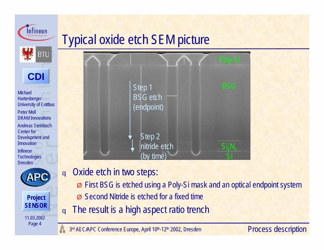
Typical oxide etch SEM picture
q Oxide etch in two steps:Ø First BSG is etched using a Poly-Si mask and an optical endpoint systemØ Second Nitride is etched for a fixed time
q The result is a high aspect ratio trench
11.03.2002Page 5
MichaelHartenbergerUniversity of CottbusPeter MollDRAM InnovationsAndreas SteinbachCenter forDevelopment andInnovationInfineonTechnologiesDresden
3rd AEC/APC Conference Europe, April 10th-12th 2002, Dresden
CDI
ProjectSENSOR
APCAPC
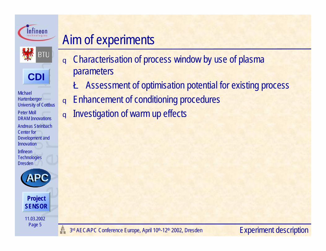
Aim of experimentsq Characterisation of process window by use of plasma
parametersè Assessment of optimisation potential for existing process
q Enhancement of conditioning proceduresq Investigation of warm up effects
Experiment description
11.03.2002Page 6
MichaelHartenbergerUniversity of CottbusPeter MollDRAM InnovationsAndreas SteinbachCenter forDevelopment andInnovationInfineonTechnologiesDresden
3rd AEC/APC Conference Europe, April 10th-12th 2002, Dresden
CDI
ProjectSENSOR
APCAPC
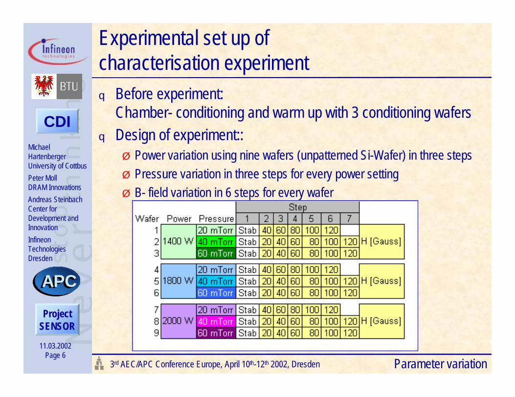
Experimental set up ofcharacterisation experimentq Before experiment:
Chamber- conditioning and warm up with 3 conditioning wafersq Design of experiment::
Ø Power variation using nine wafers (unpatterned Si-Wafer) in three stepsØ Pressure variation in three steps for every power settingØ B- field variation in 6 steps for every wafer
Parameter variation
11.03.2002Page 7
MichaelHartenbergerUniversity of CottbusPeter MollDRAM InnovationsAndreas SteinbachCenter forDevelopment andInnovationInfineonTechnologiesDresden
3rd AEC/APC Conference Europe, April 10th-12th 2002, Dresden
CDI
ProjectSENSOR
APCAPC
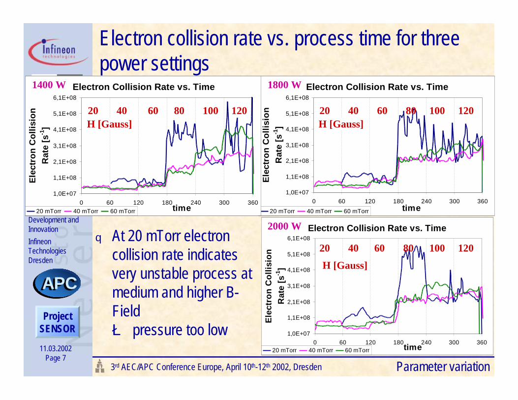
Electron collision rate vs. process time for threepower settings
q At 20 mTorr electroncollision rate indicatesvery unstable process atmedium and higher B-Fieldè pressure too low
Parameter variation
Electron Collision Rate vs. Time
1,0E+07
1,1E+08
2,1E+08
3,1E+08
4,1E+08
5,1E+08
6,1E+08
0 60 120 180 240 300 360time
Elec
tron
Col
lisio
n R
ate
[s-1
]
20 mTorr 40 mTorr 60 mTorr
Electron Collision Rate vs. Time
1,0E+07
1,1E+08
2,1E+08
3,1E+08
4,1E+08
5,1E+08
6,1E+08
0 60 120 180 240 300 360time
Elec
tron
Col
lisio
n R
ate
[s-1
]
20 mTorr 40 mTorr 60 mTorr
Electron Collision Rate vs. Time
1,0E+07
1,1E+08
2,1E+08
3,1E+08
4,1E+08
5,1E+08
6,1E+08
0 60 120 180 240 300 360time
Elec
tron
Col
lisio
n R
ate
[s-1
]
20 mTorr 40 mTorr 60 mTorr
20 40 60 80 100 120
20 40 60 80 100 12020 40 60 80 100 120H [Gauss]
1400 W
H [Gauss]
1800 W
H [Gauss]
2000 W
11.03.2002Page 8
MichaelHartenbergerUniversity of CottbusPeter MollDRAM InnovationsAndreas SteinbachCenter forDevelopment andInnovationInfineonTechnologiesDresden
3rd AEC/APC Conference Europe, April 10th-12th 2002, Dresden
CDI
ProjectSENSOR
APCAPC
Electron collision rate vs.B-Field and Pressure (1400W)
Pressure [mTorr]H [Gauss]
Electron collision rate [s-1]
20
40
60
040
80120
1e8
2e8
3e8
4e8
5e8
Electron collision rate vs.B-Field and Pressure (1800W)
Pressure [mTorr]H [Gauss]
Electron collision rate [s -1]
20
40
60
040
80120
1e8
2e8
3e8
4e8
5e8
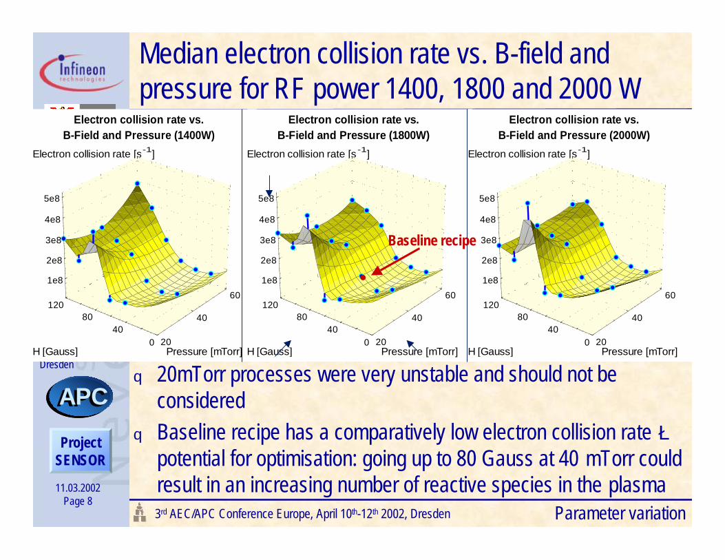
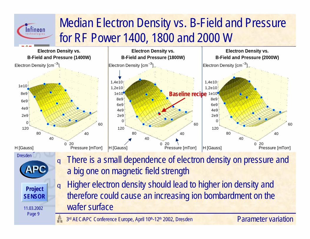
Median electron collision rate vs. B-field andpressure for RF power 1400, 1800 and 2000 W
Electron collision rate vs.B-Field and Pressure (2000W)
Pressure [mTorr]H [Gauss]
Electron collision rate [s-1]
20
40
60
040
80120
1e8
2e8
3e8
4e8
5e8
q 20mTorr processes were very unstable and should not beconsidered
q Baseline recipe has a comparatively low electron collision rate èpotential for optimisation: going up to 80 Gauss at 40 mTorr couldresult in an increasing number of reactive species in the plasma
•
Baseline recipe
Parameter variation
11.03.2002Page 9
MichaelHartenbergerUniversity of CottbusPeter MollDRAM InnovationsAndreas SteinbachCenter forDevelopment andInnovationInfineonTechnologiesDresden
3rd AEC/APC Conference Europe, April 10th-12th 2002, Dresden
CDI
ProjectSENSOR
APCAPC
Electron Density vs.B-Field and Pressure (2000W)
Pressure [mTorr]H [Gauss]
Electron Density [cm-3]
20
40
60
040
80120
02e94e96e98e9
1e101,2e101,4e10
Median Electron Density vs. B-Field and Pressurefor RF Power 1400, 1800 and 2000 W
q There is a small dependence of electron density on pressure anda big one on magnetic field strength
q Higher electron density should lead to higher ion density andtherefore could cause an increasing ion bombardment on thewafer surface
Electron Density vs.B-Field and Pressure (1800W)
Pressure [mTorr]H [Gauss]
Electron Density [cm-3]
20
40
60
040
80120
02e94e96e98e9
1e101,2e101,4e10
•
Baseline recipe
Electron Density vs.B-Field and Pressure (1400W)
Pressure [mTorr]H [Gauss]
Electron Density [cm-3]
20
40
60
040
80120
0
2e9
4e9
6e9
8e9
1e10
Parameter variation
11.03.2002Page 10
MichaelHartenbergerUniversity of CottbusPeter MollDRAM InnovationsAndreas SteinbachCenter forDevelopment andInnovationInfineonTechnologiesDresden
3rd AEC/APC Conference Europe, April 10th-12th 2002, Dresden
CDI
ProjectSENSOR
APCAPC
Parameter variation
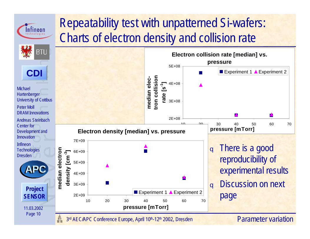
Electron collision rate [median] vs. pressure
2E+08
3E+08
4E+08
5E+08
10 20 30 40 50 60 70pressure [mTorr]
med
ian
elec
-tr
on c
ollis
ion
rate
[s-1
]
Experiment 1 Experiment 2
Electron density [median] vs. pressure
2E+09
3E+09
4E+09
5E+09
6E+09
7E+09
10 20 30 40 50 60 70
pressure [mTorr]
med
ian
elec
tron
de
nsity
[cm
-3]
Experiment 1 Experiment 2
Repeatability test with unpatterned Si-wafers:Charts of electron density and collision rate
q There is a goodreproducibility ofexperimental results
q Discussion on nextpage
11.03.2002Page 11
MichaelHartenbergerUniversity of CottbusPeter MollDRAM InnovationsAndreas SteinbachCenter forDevelopment andInnovationInfineonTechnologiesDresden
3rd AEC/APC Conference Europe, April 10th-12th 2002, Dresden
CDI
ProjectSENSOR
APCAPC
Repeatability test with unpatterned Si-wafers:explanationq Results of electron collision rate and electron density are
reproducible for 40 and 60 mTorrq Median electron density and electron collision rate for 20 mTorr
process different between experiments because of unstableprocess
è Plasma parameters allow a reliable prediction of chamberconditions
Parameter variation
11.03.2002Page 12
MichaelHartenbergerUniversity of CottbusPeter MollDRAM InnovationsAndreas SteinbachCenter forDevelopment andInnovationInfineonTechnologiesDresden
3rd AEC/APC Conference Europe, April 10th-12th 2002, Dresden
CDI
ProjectSENSOR
APCAPC
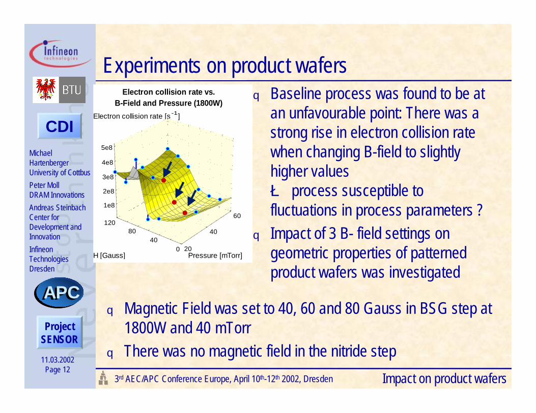
Experiments on product wafersq Baseline process was found to be at
an unfavourable point: There was astrong rise in electron collision ratewhen changing B-field to slightlyhigher valuesè process susceptible tofluctuations in process parameters ?
q Impact of 3 B- field settings ongeometric properties of patternedproduct wafers was investigated
q Magnetic Field was set to 40, 60 and 80 Gauss in BSG step at1800W and 40 mTorr
q There was no magnetic field in the nitride stepImpact on product wafers
Electron collision rate vs.B-Field and Pressure (1800W)
Pressure [mTorr]H [Gauss]
Electron collision rate [s -1]
20
40
60
040
80120
1e8
2e8
3e8
4e8
5e8
11.03.2002Page 13
MichaelHartenbergerUniversity of CottbusPeter MollDRAM InnovationsAndreas SteinbachCenter forDevelopment andInnovationInfineonTechnologiesDresden
3rd AEC/APC Conference Europe, April 10th-12th 2002, Dresden
CDI
ProjectSENSOR
APCAPC
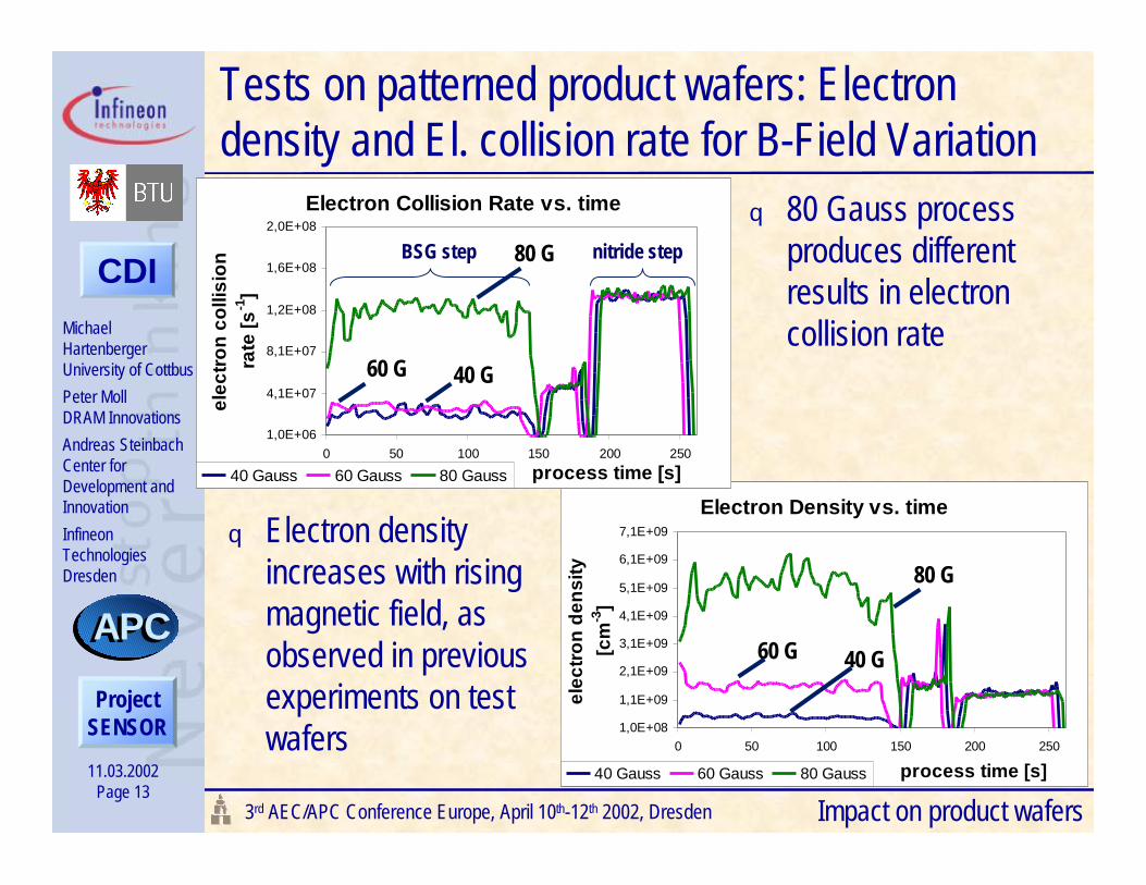
Impact on product wafers
Tests on patterned product wafers: Electrondensity and El. collision rate for B-Field Variation
q 80 Gauss processproduces differentresults in electroncollision rate
q Electron densityincreases with risingmagnetic field, asobserved in previousexperiments on testwafers
Electron Density vs. time
1,0E+08
1,1E+09
2,1E+09
3,1E+09
4,1E+09
5,1E+09
6,1E+09
7,1E+09
0 50 100 150 200 250
process time [s]
elec
tron
dens
ity[c
m-3
]
40 Gauss 60 Gauss 80 Gauss
Electron Collision Rate vs. time
1,0E+06
4,1E+07
8,1E+07
1,2E+08
1,6E+08
2,0E+08
0 50 100 150 200 250process time [s]
elec
tron
colli
sion
ra
te [s
-1]
40 Gauss 60 Gauss 80 Gauss
80 G
60 G 40 G
BSG step nitride step80 G
60 G 40 G
11.03.2002Page 14
MichaelHartenbergerUniversity of CottbusPeter MollDRAM InnovationsAndreas SteinbachCenter forDevelopment andInnovationInfineonTechnologiesDresden
3rd AEC/APC Conference Europe, April 10th-12th 2002, Dresden
CDI
ProjectSENSOR
APCAPC
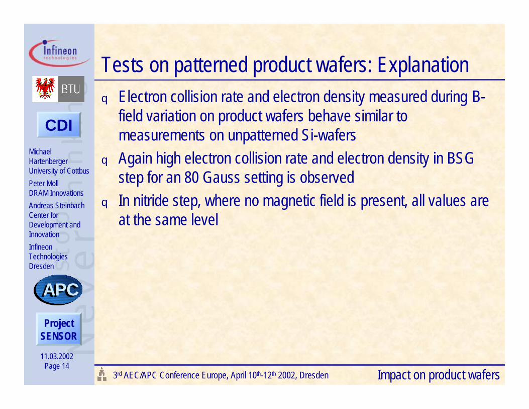
Tests on patterned product wafers: Explanationq Electron collision rate and electron density measured during B-
field variation on product wafers behave similar tomeasurements on unpatterned Si-wafers
q Again high electron collision rate and electron density in BSGstep for an 80 Gauss setting is observed
q In nitride step, where no magnetic field is present, all values areat the same level
Impact on product wafers
11.03.2002Page 15
MichaelHartenbergerUniversity of CottbusPeter MollDRAM InnovationsAndreas SteinbachCenter forDevelopment andInnovationInfineonTechnologiesDresden
3rd AEC/APC Conference Europe, April 10th-12th 2002, Dresden
CDI
ProjectSENSOR
APCAPC
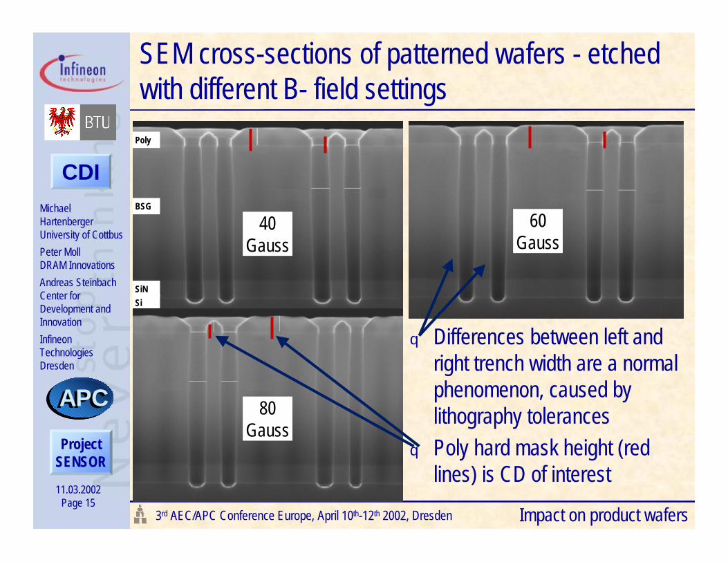
SEM cross-sections of patterned wafers - etchedwith different B- field settings
q Differences between left andright trench width are a normalphenomenon, caused bylithography tolerances
q Poly hard mask height (redlines) is CD of interest
40Gauss
Poly
BSG
SiNSi
60Gauss
80Gauss
Impact on product wafers
11.03.2002Page 16
MichaelHartenbergerUniversity of CottbusPeter MollDRAM InnovationsAndreas SteinbachCenter forDevelopment andInnovationInfineonTechnologiesDresden
3rd AEC/APC Conference Europe, April 10th-12th 2002, Dresden
CDI
ProjectSENSOR
APCAPC
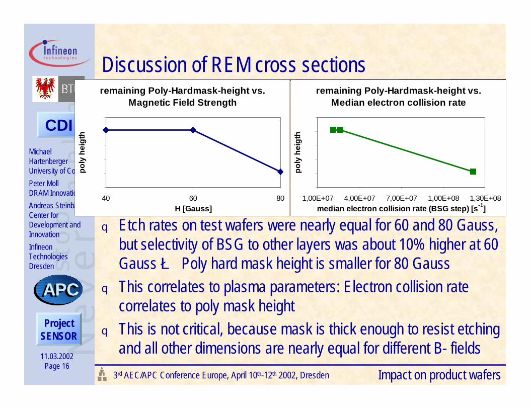
remaining Poly-Hardmask-height vs. Median electron collision rate
180
185
190
195
200
205
1,00E+07 4,00E+07 7,00E+07 1,00E+08 1,30E+08median electron collision rate (BSG step) [s-1]
poly
hei
gth
remaining Poly-Hardmask-height vs. Magnetic Field Strength
180
185
190
195
200
205
40 60 80H [Gauss]
poly
hei
gth
Discussion of REM cross sections
q Etch rates on test wafers were nearly equal for 60 and 80 Gauss,but selectivity of BSG to other layers was about 10% higher at 60Gauss è Poly hard mask height is smaller for 80 Gauss
q This correlates to plasma parameters: Electron collision ratecorrelates to poly mask height
q This is not critical, because mask is thick enough to resist etchingand all other dimensions are nearly equal for different B- fields
Impact on product wafers
11.03.2002Page 17
MichaelHartenbergerUniversity of CottbusPeter MollDRAM InnovationsAndreas SteinbachCenter forDevelopment andInnovationInfineonTechnologiesDresden
3rd AEC/APC Conference Europe, April 10th-12th 2002, Dresden
CDI
ProjectSENSOR
APCAPC
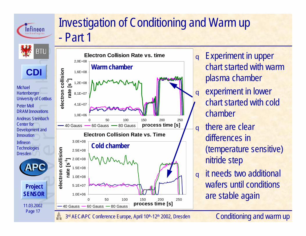
Investigation of Conditioning and Warm up- Part 1
q Experiment in upperchart started with warmplasma chamber
q experiment in lowerchart started with coldchamber
q there are cleardifferences in(temperature sensitive)nitride step
q it needs two additionalwafers until conditionsare stable again
Conditioning and warm up
Electron Collision Rate vs. Time
1.0E+06
5.1E+07
1.0E+08
1.5E+08
2.0E+08
2.5E+08
3.0E+08
0 50 100 150 200 250process time [s]
elec
tron
col
lisio
n ra
te [s
-1]
40 Gauss 60 Gauss 80 Gauss
Electron Collision Rate vs. time
1,0E+06
4,1E+07
8,1E+07
1,2E+08
1,6E+08
2,0E+08
0 50 100 150 200 250process time [s]
elec
tron
colli
sion
ra
te [s
-1]
40 Gauss 60 Gauss 80 Gauss
Warm chamber
Cold chamber
11.03.2002Page 18
MichaelHartenbergerUniversity of CottbusPeter MollDRAM InnovationsAndreas SteinbachCenter forDevelopment andInnovationInfineonTechnologiesDresden
3rd AEC/APC Conference Europe, April 10th-12th 2002, Dresden
CDI
ProjectSENSOR
APCAPC
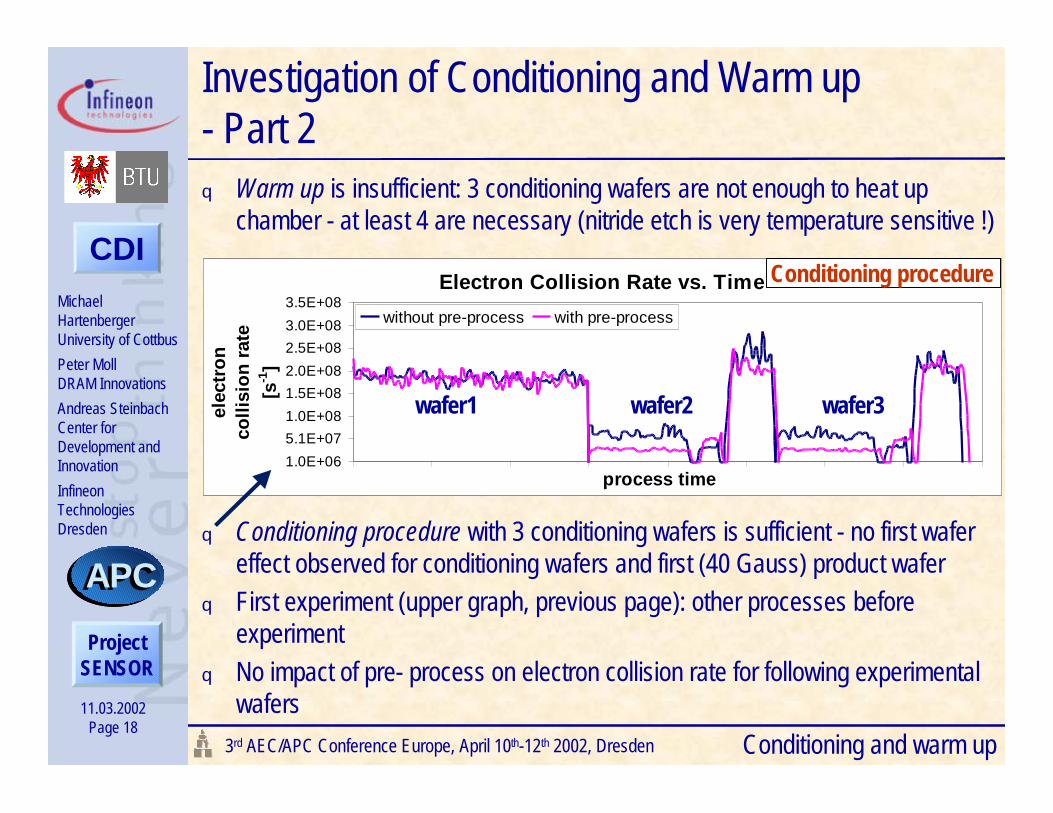
Investigation of Conditioning and Warm up- Part 2q Warm up is insufficient: 3 conditioning wafers are not enough to heat up
chamber - at least 4 are necessary (nitride etch is very temperature sensitive !)
Electron Collision Rate vs. Time
1.0E+065.1E+071.0E+081.5E+082.0E+082.5E+083.0E+083.5E+08
0 100 200 300 400 500 600 700 800process time
elec
tron
colli
sion
rate
[s
-1]
without pre-process with pre-process
Conditioning procedure
q Conditioning procedure with 3 conditioning wafers is sufficient - no first wafereffect observed for conditioning wafers and first (40 Gauss) product wafer
q First experiment (upper graph, previous page): other processes beforeexperiment
q No impact of pre- process on electron collision rate for following experimentalwafers
wafer1 wafer2 wafer3
Conditioning and warm up
11.03.2002Page 19
MichaelHartenbergerUniversity of CottbusPeter MollDRAM InnovationsAndreas SteinbachCenter forDevelopment andInnovationInfineonTechnologiesDresden
3rd AEC/APC Conference Europe, April 10th-12th 2002, Dresden
CDI
ProjectSENSOR
APCAPC
Benefit of plasma parameter measurementq Plasma parameters were used to characterise oxide etch process by
parameter variation and showed potential for process developmentand optimisation.
q They indicated temperature and conditioning effects è they are apowerful tool to verify conditioning and warm up procedures withminimal effort in real time.
q It was shown that plasma parameters give reproducible results andcan be used for stability control and failure detection.
q Additional measurement techniques are necessary for investigationof chemical reactions, e.g., optical emission spectroscopy.
q Correlation to selectivity was shown è plasma parameters can beused to optimise processes
Benefit
11.03.2002Page 20
MichaelHartenbergerUniversity of CottbusPeter MollDRAM InnovationsAndreas SteinbachCenter forDevelopment andInnovationInfineonTechnologiesDresden
3rd AEC/APC Conference Europe, April 10th-12th 2002, Dresden
CDI
ProjectSENSOR
APCAPC
Summaryq An oxide etch process has been characterised using plasma
parameters electron collision rate and electron density byvariation of pressure, power and B- field.
q Unstable processes have been found for a pressure of 20mTorr- this pressure should be avoided for wafer processing.
q Experiments on product wafers showed a correlation of plasmaparameters to remaining Poly-Si thickness and selectivity.
q 60 Gauss process is recommended, because its selectivity ishighest.
q Conditioning procedure with two conditioning wafers is sufficientto eliminate pre-process influence on products.
q Warm up procedure with two conditioning wafers is insufficient -strong temperature influence has been found.
Summary