application of ip-based analog platforms in the design of
TRANSCRIPT

HAL Id: hal-00765898https://hal.archives-ouvertes.fr/hal-00765898
Submitted on 17 Dec 2012
HAL is a multi-disciplinary open accessarchive for the deposit and dissemination of sci-entific research documents, whether they are pub-lished or not. The documents may come fromteaching and research institutions in France orabroad, or from public or private research centers.
L’archive ouverte pluridisciplinaire HAL, estdestinée au dépôt et à la diffusion de documentsscientifiques de niveau recherche, publiés ou non,émanant des établissements d’enseignement et derecherche français ou étrangers, des laboratoirespublics ou privés.
Application of IP-based Analog Platforms in the designof Neuromimetic Integrated Circuits
Timothée Levi, Noëlle Lewis, Jean Tomas, Sylvie Renaud
To cite this version:Timothée Levi, Noëlle Lewis, Jean Tomas, Sylvie Renaud. Application of IP-based Analog Platformsin the design of Neuromimetic Integrated Circuits. IEEE Transactions on Computer-Aided Design ofIntegrated Circuits and Systems, IEEE, 2012, 31 (11), pp.1629 - 1641. �10.1109/TCAD.2012.2204992�.�hal-00765898�

TCAD-2011-0412
1
Affiliation: T. Levi is with the IMS laboratory, UMR CNRS 5218,
University of Bordeaux, Talence, FR 33400, FRANCE. (phone: +33 54000 2773; fax: +33 5 5637 1545; e-mail: [email protected]). N. Lewis is with the IMS laboratory, UMR CNRS 5218,
University of Bordeaux, Talence, FR 33400, FRANCE (e-mail: [email protected]). J. Tomas is with IMS laboratory, UMR CNRS 5218,
University of Bordeaux, Talence, FR 33400, FRANCE (e-mail: [email protected]). S. Renaud is with the IMS laboratory, UMR CNRS 5218,
University of Bordeaux, Talence, FR 33400, FRANCE (e-mail: [email protected]). No preliminary versions have been published Final version of the paper (after 2 revisions)
Manuscript received July 28, 2011, first revision on October 30, 2011,
second revised and re-submitted March 12, 2012, final version June 1, 2012.
T. Lévi is with the IMS laboratory, UMR CNRS 5218, University of
Bordeaux, Talence, FR 33400, FRANCE. (phone: +33 5 4000 2773; fax: +33
5 5637 1545; e-mail: [email protected]).
N. Lewis is with the IMS laboratory, UMR CNRS 5218, University of
Bordeaux, Talence, FR 33400, FRANCE (e-mail: noelle.lewis@ims-
bordeaux.fr).
J. Tomas is with the IMS laboratory, UMR CNRS 5218, University of
Bordeaux, Talence, FR 33400, FRANCE (e-mail: jean.tomas@ims-
bordeaux.fr).
S. Renaud is with the IMS laboratory, UMR CNRS 5218, University of
Bordeaux, Talence, FR 33400, FRANCE (e-mail: sylvie.renaud@ims-
bordeaux.fr).
Application of IP-based Analog Platforms in the
design of Neuromimetic Integrated Circuits
Timothée Levi, Noëlle Lewis Member IEEE, Jean Tomas, and Sylvie Renaud Member IEEE

TCAD-2011-0412
2
Abstract— Re-use methodologies are now widely used to design
digital circuits. They are based on the concept of Intellectual
Property (IP), or virtual block of computing, characterized by a
behavioral model, synthesizable or not. The design re-use for
analog integrated systems is much less natural and less
standardized. This paper addresses the issue of an analog design
flow based on re-use, focusing on those three key questions: the
formal content of the IP block, the design of a re-usable analog IP
and finally the organization of a design flow centered on an IP
library. After a conceptual overview, this paper presents the
methodological principles and details examples with a tutorial
intention. The objective is to guide the designer involved in the
process of developing analog IPs and corresponding design flow.
The method is inspired from platform-based design and adapted
here on an original case study: the design of full-custom
neuromimetic integrated circuits, built from specific analog
computational blocks. The development of re-usable IPs
represents an additional effort, mainly for behavioral modeling
and characterization. Nevertheless, the steps illustrated in this
case study show that the extra time provides a definite advantage
for future design projects.
Index Terms—Analog_circuits, CAD, Design Re-use,
Neuromimetic Circuits and Systems, Behavioral and multi-
domain simulation.
I. RE-USE METHODOLOGY FOR CIRCUIT AND SYSTEM DESIGN
HANKS to the growing improvements in semi-conductor
manufacturing processes nowadays, VLSI circuits can
reach a high level of complexity. The design methodologies
have also considerably evolved to allow System-on-Chip
(SoC) integration. The SoC design flow is mainly based on re-
usable components, called Intellectual Property (IP) blocks or
cores, which are now well defined and widely used in the
digital domain [1]. They are classified from Soft to Hard IP;
Soft IP refers to synthesizable HDL (Hardware Description
Language) description and a Hard IP is a layout level design.
The Firm IP corresponds to an intermediate level, and refers to
a pre-synthesized block, using generic components, with a
remaining degree of optimization respecting the technology
specifications [2]. The advantages of Soft IPs are flexibility
and portability, but their real behavior depends on the physical
implementation; at the opposite, Hard IPs are optimized for a
specific application, on a target technology, consequently they
have a predictable behavior.
Moreover, digital design flow is much more automated than
the analog one. Digital design profits from standardized tools
and methods which allow automatic synthesis. While the trend
over the past years has been to integrate both digital and
analog circuits on the same chip, the analog part is always the
most costly in terms of design effort.
Fig. 1 was extracted from a report on Design topic of
International Technology Roadmap for Semiconductors
(ITRS) [3]. It illustrates the traditional V-cycle of system
design, from specification to layout, with intermediate
abstraction levels called behavioral and circuit levels. The top-
down way is known as synthesis flow and the bottom-up way
as verification flow. This compact picture summarizes the
maturity difference between digital and analog design flows
and emphasizes future requirements for Electronic Design
Automation (EDA). For digital circuits there is a lack of
methods and tools at the highest level of the hierarchy,
(executable specifications and whole system verification
procedures for example); for analog circuits, complete
solutions are rarely found at all level of abstractions.
Automation of the analog design process is still an open
challenge, and re-use methodology is a predominant
recommendation.
Important conceptual advances have been proposed in the
last twenty years, with precursor works of [12] and [15],
resulting in effective software solutions. Our work was guided
by these concepts and developments, and also took into
account the specificities of neuromimetics circuits and
systems. Our background material results from a 20 years
experience in our research group in this field of neuromorphic
engineering [4] [5]. It consists in particular in a library of
analog computation blocks used to design analog ASICs
(Application Specific Integrated Circuit) that mimic the
dynamics of biological neurons electrical activity [6]. Those
blocks were initially described by their electrical schematic
and physical layout; we name it the “initial Hard IP.” Starting
from this background material, we intended to build a
dedicated design platform, to automate the design of future
neuromimetic ASICs. As demonstrated later, this context is
very favorable to the development of a library of Firm IPs, and
finally the implementation of an IP-based design flow.
Application of IP-based Analog Platforms in the
design of Neuromimetic Integrated Circuits
Timothée Levi, Noëlle Lewis Member IEEE, Jean Tomas, and Sylvie Renaud Member IEEE
T

TCAD-2011-0412
3
The paper is organized as follows: in section II, a state-of-
the-art review describes the main concepts and solutions
regarding analog design synthesis, and points out issues related
to IP re-use in the analog domain. Preliminary tasks for the
implementation of the design flow are discussed in section III.
Then, we define our methodology in 3 points: the IP-package
content (section IV), the design of a re-usable IP block
(section V) and the integration of an IP in the system design
flow (section VI). Concrete application of the methodology is
given in section VII, through examples of design projects [4].
Specification
Architecture
Partitioning
Testbench
Behavioral
Description
Ciruit
Netlist
Layout
Software Software
Sensor/
Actuator
Sensor/
Actuator
ITRS Design 2009
available
partially available
missing
digital design
Specification
Architecture
Partitioning
Testbench
Behavioral
Description
Ciruit
Netlist
Layout
Software Software
Sensor/
Actuator
Sensor/
Actuator
ITRS Design 2009
available
partially available
missing
digital design
Specification
Architecture
Partitioning
Testbench
Behavioral
Description
Ciruit
Netlist
Layout
Software Software
Sensor/
Actuator
Sensor/
Actuator
available
partially available
missing
analog design
ITRS Design 2009
analog design
Specification
Architecture
Partitioning
Testbench
Behavioral
Description
Ciruit
Netlist
Layout
Software Software
Sensor/
Actuator
Sensor/
Actuator
available
partially available
missing
analog design
ITRS Design 2009
analog design
Figure 1. System-Level Design Potential Solutions for digital and analog
flow from ITRS Design 2009 [3]
II. STATE-OF-THE-ART REVIEW : BACKGROUND CONCEPTS AND
ISSUES FOR ANALOG IP RE-USE
A. Background concepts for analog design flow automation
Before addressing the specifications of an analog IP-based
design framework, let us overview the possible approaches to
improve the analog design flow for VLSI and reach the
automatic analog synthesis.
First, directly inspired from the success story of digital
design using FPGAs, we would like to mention the FPAA
(Field Programmable Analog Array) technology [7]. Its
principle is very efficient for the rapid prototyping of state-of-
the-art analog functions; it can’t be yet applied to our
application domain, which requires very specific functional
blocks.
Then, concerning analog ASIC design automation, the main
problem is the optimization of one architecture or topology for
a set of specifications. Two ways are then possible for this
optimization: simulation-based [8], [9] or knowledge-based.
The first one sizes a given schematic by a closed-loop process
with an optimizer, an analog simulator and standard transistor
models. The drawbacks are intensive simulations, CPU time
and the selection of the design parameters among a huge list.
Analog designers are generally more interested in knowledge-
based optimization, to keep control over the choice of
parameters. This was also our choice. A review of knowledge-
based synthesis tools can be found in [10]. In such an
approach, the designer must identify (i) a useful subset of
design parameters in relation to the targeted performances, (ii)
the circuit equations, and (iii) the sizing procedure.
The circuit equations are supposed to relate the performance
parameters to the design parameters. This point is a non-trivial
issue, which involves simplification algorithms and more or
less insights in the circuit operation [11], [12], [13]. As
explained in section IV, our approach leads to multi-level
modeling, starting from the ideal functional equation (given by
neuroscientists in our case), with gradual refinement to
behavioral equations. We use mainly the technique of user-
defined equations and sometimes a simulation-based
technique coupled with regression.
The circuit sizing process generally happens after topology
selection. It starts from an un-sized schematic and follows the
designer’s steps to set a sized schematic, responding to the
specifications. Layout generation, as the final design step, is
often a separate task and rarely included in the sizing
procedure [14].
For complex integrated circuit, up to the system level, a
hierarchy of abstraction levels must be defined and the top-
down/bottom-up design flows may be combined in different
ways. One can propagate the constraints down starting from
top-level to the schematic and layout [15], [16], [17]. Another
solution is to merge top-down and bottom-up flows in a meet-
in-the-middle approach, which is the principle of platform-
based design [18], [19]. This method relies on a library of
components, well characterized and abstracted in a set of
models, used for a bottom-up phase. Then the top-down phase
consists in selecting the optimal component, according to some
cost function, that satisfies all constraints.
Two main reasons justified our choice to build such a design
platform. The first one is related to our specific application
field of neuromimetic ASICs. Such devices require the use of
non-traditional analog functional blocks, different from OTAs
or OPAMPs. In addition, to ensure stability throughout long-
term projects in this field, we could start from functional
modules already identified and sized for previous projects [6].

TCAD-2011-0412
4
So we did not question the sizing procedure from the
beginning but rather decided to characterize the ability to re-
use these blocks; in other words, the question was how to
transform a library of Hard IPs (schematic and layout) in a
library of Firm IPs and how to implement an automated flow
for further design projects.
B. What kind of IP for an analog block?
The notion of analog IP for automation of analog design
flow was the subject of numerous debates [20], [21], [22], [23]
and [24].
Ideally, the analog design flow should be identical to the
digital one, but this is not the case yet. Of course, the initial
context is different and the rules based on analog design are
more difficult than Boole algebra. The designer has to
challenge non-linear functional relationships, technological
parameters and various second order sensitivities [25], [26]
(temperature, noise, mismatch, etc.). Analog signal processing
is more performing in terms of speed and power consumption
but its design is more difficult, closely linked to designer’s
knowledge. An analog block is designed for a specific
application. Consequently there is no consensus on the analog
design processes and the primitive functions could be very
different depending on cases: current or voltage design mode,
bipolar or CMOS design, strong or weak inversion mode for
CMOS transistors, etc.
A clear definition of what should contain an analog IP is
therefore the starting point for a productive, capable reuse-
based design framework for analog ICs. The 3 classes of
digital IPs have been exposed in the introduction. Let us see
hereafter, the pertinence of this classification for the analog
case.
1) Hard IP?
Among the typical operators in analog design, we can find
operational amplifiers, ADC and DAC convertors, PLLs,
filters, voltage references and RF modules. These blocks are
usually optimized in consumption and area for one specific
application: the natural trend in analog design is then Hard IP.
This type of IP had been chosen in the guide of design and
documentation steps by VSIA consortium in 2001 [27].
In this case, technology migrations are solved by re-design
instead of re-use.
2) Soft IP?
What could be a Soft-IP in analog design? We can describe
in HDL design language one analog block with the selected
functionality. The issue is that there is currently no universal
synthesis process which delivers a sized electrical schematic
for one application. Furthermore, we first have to select a
design mode (current mode, voltage mode), choose primitive
functional blocks and select one topology for each. One
helping tool capable of enabling the designer to choose one
topology among different possibilities would be a great step
for the analog synthesis. Promising work about analog circuit
sizing method using interval analysis could solve this issue
[28] and allow selecting or deleting some topologies.
Nevertheless, before creating this selection tool, a database
should be build, with adequate documentation for each
topology.
3) Firm IP?
Between the Soft and the Hard-IP, we find the Firm-IP
which seems to be the best choice for analog design. It is a
compromise between a fixed layout and a purely HDL
description. It proposes a design based on electrical schematic,
with enough tunable characteristics to be re-usable for several
applications.
C. State-of-the-art review
Questions arising from the development of an IP-based
analog design flow can be illustrated by Fig. 2. The IP Library
is the central point; it is filled by the Analog IP Design Flow
and it interacts with the System Design Flow. Then, the first
task is to define (1) what kind of information should be
embedded in the IP and in which format. After that, it is
important to emphasize (2) the design methodology of a re-
usable IP, because it differs from the design methodology of a
“one-shot” circuit. And the last point is (3) the re-use of an IP
in the system design flow.
System
Spécifications
Architectures
IPs selection IP-Based
Library
IP-Based
Library
Analog IP
Design flow
Analog IP
Design flow
Verification
Requests
Selection
Behavioural models
Block
specifications
Topology
selection
Sizing
Layout
System design flow
System
Spécifications
Architectures
IPs selection IP-Based
Library
IP-Based
Library
Analog IP
Design flow
Analog IP
Design flow
Verification
Requests
Selection
Behavioural models
Block
specifications
Topology
selection
Sizing
Layout
System
Spécifications
Architectures
IPs selection IP-Based
Library
IP-Based
Library
Analog IP
Design flow
Analog IP
Design flow
Verification
Requests
Selection
Behavioural models
Block
specifications
Topology
selection
Sizing
Layout
System design flow
Figure 2. First-preview of an analog IP-based design flow
First, we propose to review how these three points have
been addressed by the main contributions that could be found
in the literature.
1) IP-package content
This point deals with the IP general information, including
characteristic parameters, design knowledge, models,
description formats adapted to every step of the design flow
(architecture simulation, sizing, verification, and layout).
O’Connor et al. [29], [30], [31] have defined as analog IP
content:
- Set of descriptive views: input/output ports, functional
model, structural model
- Set of parameters: for electrical performances, electrical
and physical design
- Set of relationships and calculation methods between
these parameters.
Evaluation methodology allows the translation from

TCAD-2011-0412
5
physical to performance parameters. Extraction methodology
allows the translation from simulations to performance
parameters. Synthesis methodology allows the translation from
performance to design parameters. Constraint distribution
methodology formalizes the translation from IP to under-block
specifications.
These relationships are built from the designer knowledge
and the main challenge is to express it. This knowledge could
be written in an analytical form with an approach based on
experiences, or in a procedural form with an approach based
on extensive simulations and optimization. This analog IP
definition has been applied to amplifier circuits included in a
chain of CMOS photo-reception and used to demonstrate the
possibility of an automated hierarchical synthesis, in the field
of interconnection optical systems.
Secondly, Castro-Lopez et al. [17], [32] have defined an
analog IP that contains a behavioral model, a sized schematic
and a layout. As this IP is developed for a specific technology,
this definition is close to what we consider as Hard IP.
Third, Hamour et al. [33] have proposed an IP definition
including similar views: sized schematic, behavioral model,
test bench model, but no layout.
Pimentel et al. [34] describe the content of analog and
mixed signal IPs: one IP could be divided into three parts:
models (functional, behavioral and structural), documents
(basic information, user, creation and test guides, physical
implementation and models) and circuit schematics.
2) The design of one IP
This point is important for guiding the designer in the
different development steps of a re-usable block [35].
Analyzing the experience design to make it re-usable is a
complex task. In particular, formalizing the sizing process is a
critical step.
Louërat et al. have developed a tool named CAIRO+, which
is a platform of analog IP re-use [36], [37]. First, the designer
has to describe his circuit into an electrical schematic, a set of
sizing parameters and a floor plan layout. CAIRO+ tool can
make an automatic sizing and layout, depending on
technological parameters, if the procedural sizing steps have
been described beforehand. This task is assisted by a synthesis
methodology developed in the dissertation of R. Iskander [10].
3) Integration of an IP in the system design flow
What are the main issues related to this point? First, from
the architecture exploration to the verification step, it is
mandatory to manage different abstraction levels of the IP.
Another point is the storage of IPs into a data base which
could be queried according to an adequate exploration method.
Besides these questions, interesting approaches of Firm IP
hardening flow have been developed, by two previously cited
teams. With Louërat et al., the IP description in CAIRO+ is
parametric and described into equations then the Hard IP is
automated and needn’t optimization. Some examples are in the
Nguyen-Tuong dissertation [14]. With O’Connor et al., the
synthesis process is described with UML language and it is
included into the design platform (RUNE II) which contains
simulation and optimization tools [38].
Note that, despite the general trend is to design a library of
Firm IPs, a specific adjustable functional component, the
answers to the previous three main questions depend on the
initial IP point of view. The method used to reach the desired
Firm IP differs in two ways: in some cases the notion of Firm
IP is progressively derived from a Soft IP view, while in other
cases it is derived from an initial Hard-IPs library. Our
approach belongs to this second case. Indeed our background
material was a library of blocks listing 3 views: symbol,
schematic and layout. As explained in section I, the issue here
was to transform a library of Hard IPs in a library of Firm IPs.
The critical points in the proposed process are: multi-level
modeling, characterization of validity range to fit requested
performances. Finally we implemented a system design flow,
based on the automated exploration of an IP database. We are
now going to detail step by step the process methodology.
III. PRELIMINARY TASKS TO ESTABLISH THE DESIGN FLOW
Preparatory tasks are required to structure and finally
establish an IP-based design flow. The first one is to define the
system hierarchy and the primitive blocks, which are
associated to each level of this hierarchy. The second one is to
define a set of typical specifications that constrains the circuit
performances. This part will describe these preliminary issues,
with examples taken from our application context of
neuromorphic engineering.
A. The specific context of neuromorphic engineering
The originality of that work relies on this particular
application domain: the design of analog ASICs that are
involved in neuromorphic systems. The goal of neuromorphic
engineering is to develop integrated circuits and systems that
emulate the electrical activity of biological neural networks.
From the microelectronic point of view, one solution is to
design analog ASICs for real-time computation of neurons’
activity and to digitally control the connectivity between these
neurons. We focus here on a series of analog ASICs that
implement an electro-physiological neuron model, inspired
from the Hodgkin-Huxley (HH) formalism [39]. They are
typically used as hardware simulators in computational
neurosciences, in order to explore information coding and
adaptation principles in the brain [40].
This domain has appeared to be a favorable background to
the development of a design flow based on IP-reuse. The main
reason is that the bases of system hierarchy and design
primitives have been clearly established, along successive
design projects [5]. This point is finally similar to the reality of
digital design and it should be the first requirement of the
methodology: what is the system hierarchy and what are the

TCAD-2011-0412
6
primitives at each hierarchical level?
B. Design primitives and system hierarchy
The principle of the modular design of the neuromimetic
ASICs has been already exposed in [6]. The architecture of
one ASIC is based on the repetition of a small number of
computation primitives, namely sigmoid, kinetic, power,
output (see Fig.3). One can consider them as a first version of
the IP blocks, on the form of Hard IPs, that were realized on
AMS BiCMOS 0.35 m process. Each of these elementary
cells is an analog operator involved in the equations of the
Hodgkin-Huxley formalism. These analog operators are then
assembled to produce a so-called neuromimetic ASIC, capable
of emulating, in real-time, the dynamics of a small neuron’s
network.
Figure 3. Correspondence between mathematical function and electrical
implementation, for each type of Cell Level IP. All the voltages (Vmem, Voffset,
Vequi, Vslope) are in Volt in biological expression and are multiplied by 5 for
electronic correspondence. The time constant (τ) is the same in electronical
and biological fields. The conductance (gmax) is in Siemens in biological
expression and multiplied by 10 in its electronic counterpart. m is a
probability (unitless) in biological model and it is a current (Ampere) in
electronic. p and q are integers in both electronic and biological expressions.
Fig. 3 shows the correspondence between the mathematical
function of the HH model and the analog cells that are used for
its realization. Note the choice of a current mode design. Vmem
is the membrane potential of the neuron, while Voffset and Vslope
are input voltages used to tune the neuron model parameters. τ
is the kinetic of the activation/inactivation of ionic current.
gmax is the maximum conductance, and m and h represent the
activation and inactivation terms, respectively. Dynamic
functions describe the permeability of membrane channels to
its specific ion. Vequi is the ion-specific reverse potential and p
and q are integers. m relaxes back toward its associated steady-
state value m, which is a sigmoid function of Vmem.
Starting from the previous basic operators, it is possible to
construct the hierarchy of an integrated circuit that emulates a
biologically realistic neural network: this hierarchy is
described on Fig.4. The IP level corresponds to the recurrent
computation blocks of Fig. 3 and the higher hierarchical levels
of rank N+1 are simply structural descriptions using the
primitive blocks of level N.
Figure 4. ASIC hierarchy and related neuronal computation blocks
C. System specifications and IP-block performances
The specifications of such a system are slightly non-typical,
regarding the traditional analog design field. The
neuroscientists interested in those systems want to fix:
- the number of neurons defining the network: N
(defined at System Level)
- the number and type of ionic channels considered for
each neuron: Na conductance (Sodium channel), K
conductance (Potassium channel), Leak conductance
(Leak channel) and Slow conductance (additive channel
for calcium dependence)
(defined at Macro-block level)
- the number of synapses Ns for each neuron and their
electrophysiological parameters: τ, Vequi and gmax.
(defined at Macro-block level)
- the electrophysiological parameters of each ionic channel:
Voffset, Vslope, τ, Vequi and gmax.
(defined at Block Level and propagated to Cell Level).
Let us note that for the Na conductance and Slow
conductance, the parameters Voffset, Vslope and τ, are
duplicated because of two concurrent processes in the
neurophysiology, named activation and inactivation.
A typical specifications set is given on Table I. It
corresponds to a small circuit of two neurons: Neuron 1 has 3
ionic channels (Na, K, Leak) and Neuron 2 has one additive
channel for calcium dependence (Slow conductance).

TCAD-2011-0412
7
TABLE I
TYPICAL SPECIFICATIONS OF AN ASIC WITH A SMALL NETWORK OF 2 NEURONS
Voffset_act Vslope_act Voffset_inact Vslope_inact τ _act τ _inact Vequi gmax
Sodium -39 mV 8,55 mV -47 mV -7.3 mV 0.03 ms 0.25 ms 40 mV 0.7 µS
Potassium -27 mV 12,6 mV 3 ms -80 mV 1.4 µS
Leak 50 mV 0.5 µS
Synapse 4 ms 60 mV 0.3 µS
Synapse 5 ms 50 mV 0.2 µS
Voffset_act Vslope_act Voffset_inact Vslope_inact τ _act τ _inact Vequi gmax
Sodium -39 mV 8.55 mV -47 mV -6,6 mV 0.03 ms 0.25 ms 40 mV 0.7 µS
Potassium -27 mV 12.6 mV 3 ms -80 mV 1.4 µS
Slow conductance -55 mV 10.4 mV -38 mV -20 mV 6 ms 6 ms -100 mV 0.1 µS
Leak 50 mV 0.33 µS
Synapse 6 ms 10 mV 0.1 µS
Furthermore, the implemented neuron models must
emulate a variety of biological neuron behaviors, thus the
IP-blocks must be designed to guaranty a certain tuning
range for the electrophysiological parameters. This
constraint imposes that the IP-block functionality must be
preserved while varying the electrophysiological parameters
in the so-called validity ranges. Hence, the performances of
the IP-blocks are quite non typical and are given in terms of
these validity ranges. For example, typical performances for
sigmoid IP are given in Table II, for kinetic IP the time
constant range have to be [τ, 50 τ] and for output IP the
transconductance range [gmax, 50 gmax].
TABLE II
TYPICAL PERFORMANCES OF SIGMOÏD IP, IN THE FORM OF VALIDITY RANGE
FOR INPUT VOLTAGES WITH A SUPPLY VOLTAGE OF 5 V
Performances
parameters
Minimum Maximum
Vmem 0.5 V 4.5 V
Voffset 1.5 V 3.3 V
Kslope 1.7 V 4.7 V
After this introduction, required to efficiently prepare the
implementation of an IP-based design flow, we will now
consider in details the three main points of the methodology.
IV. ANALOG IP PACKAGE
As explained in part II, our approach is to build Firm IPs
starting from Hard IPs (only symbol, schematic and layout)
that have previously been designed and optimized for a given
project. So the question is: how can we transform a Hard IP to
a Firm IP? Based on our experience, combined with the
proposed studies in the literature, it appears that the main
properties required for a re-usable IP are:
- ease of simulation at each level of abstraction of the
system,
- description of the design process and
- ability to resize the IP to deal with a technology migration
or a change in specifications.
In our methodology, each Firm IP we created has 7
informative views that are described in Table III. The views
Symbol, Schematic and Layout were already present in the
Hard IPs library. The new Firm IP package contains additive
description views that correspond to hierarchical abstraction
models (Connectical, Functional and Behavioral). These
models are developed by the designer, in a standard design
language. In our case, we use the Verilog-A language [41]. In
order to have a fluent design flow, all these views have the
same terminals and the same symbol as the schematic. These
views are useful for multilevel simulations especially in the
verification phase of the design process. The Functional view
describes the ideal equations of the function to be
implemented. The Behavioral view is more detailed and
contains refined equations that fit the circuit non-ideal
behavior [42], [43]. The Connectical view is an empty model
used to verify that blocks are well connected, without any
functional equations. It is used for the ultimate verifications,
when the overall ASIC needs to be simulated. TABLE III
INFORMATIVE VIEWS EMBEDDED IN THE ANALOGUE IP PACKAGE
View name Description and role Format
Symbol visualizes the function graphical
Connectical verifies connection between
blocks
Verilog-A
Functional models ideal electrical behavior Verilog-A
Behavioral models non-ideal electrical
behavior, extracted from
schematic
Verilog-A
Schematic transistor-level schematic graphical /
netlist
Layout physical design in targeted
technology
graphical /
GDS-II
Documentation design knowledge formulation text
To emphasize the re-usability of one IP, we also add a last
file, namely the Documentation view. This file finally collects
the design expertise and contains data such as:
- the performance and design parameters
- the design procedure and sizing algorithm (or how to link
the performance parameters to the design parameters)
- the characterization of the block with the objective of re-
use (what are the performances, how to measure them,

TCAD-2011-0412
8
and how far the circuit functionality is stable regarding
operational changes)
- information that concerns the already designed layout
view (technology, supply voltage, area and cost).
V. DESIGN OF A RE-USABLE IP
Design for re-use is not limited to the design and sizing of a
“one-shot” circuit (Hard IP case). An additional effort is
required to obtain a Firm-IP; in our case it is to express the
design procedure, to develop hierarchical models, to
characterize the circuit and to write the documentation file.
This methodology is presented here using the example block
sigmoid.
A. Design procedure of one IP
The expression of design expertise is essential to make an IP
re-usable. The topology of the circuit being given, we must
begin by identifying the performance parameters of the block
(the parameters that are constrained by specifications) and the
design parameters (those that can be adjusted in the design
procedure); then explain how the design parameters are linked
to the performance parameters. Let develop this point on the
sigmoid block.
As mentioned in Fig. 3, the mathematical function of the
HH formalism to imitate is the following:
Vslope
VoffsetVmemmem
e
Vm)(
1
1)(
(1)
In practice, one chooses to represent the variable m∞ with a
normalized current 2I0. The electrical functional equation
becomes:
Vslope
VoffsetVmemm
e
II
)(
0
1
2
(2)
The topology chosen to emulate this function is based on a
differential pair which takes direct input voltages Vmem and
Voffset. The slope control parameter Vslope of the model is
generated through a current-voltage converter, controlled by
the Kslope voltage [5]. The Schematic view is given below by
Fig. 5:
Figure 5. Schematic view of sigmoid Cell level IP
The first and second sub-blocks are finally described by the
following functional equations:
slope
slope
slopeR
KVccI
(3)
slopeT IUR
VoffsetVmemIrsig
e
II
..
).(.
02,1
0
1
2
(4)
Thus the tuning of the Vslope parameter is made using the
following equation where UT is the thermal voltage (≈25 mV at
25 °C):
slope
slopeTslope
R
KVcc
Ir
URV
0
(5)
We can extract the parameters needed for this design
procedure. The performance parameters are Vmem, Voffset, Vslope
(or Kslope which is linearly related to Vslope). The design
parameters are: Rslope, R, r and I0. The previous equations are
used to connect those two sets of parameters using a method
based on knowledge.
B. Multi-level modeling of one IP
As explained previously, models are considered at 3 levels
of abstraction and are written in Verilog-AMS. Using the
example of the sigmoid block, the Functional model
reproduces the functional equations of the preceding paragraph
(3), (4), (5). For the Behavioral model, the input and output
impedances are included as well as non-ideal effects. For
instance, in this sigmoid block, we add the non-ideal gain of
the op-amp in the voltage-current converter, the unbalanced
differential pairs and the copy factor errors of current mirrors.
All that non-ideals characteristics are extracted from electrical
simulations of Schematic view.

TCAD-2011-0412
9
The Connectical view is at a higher abstraction level; it is a
virtually empty block, simply being responsible for detecting
defaults of connection between blocks. The principle consists
in verifying that the voltages and currents applied to the block
lie within a plausible range, and if so, the output is set to a
nominal value, if not it is set to zero.
Simulations with multiple levels of abstraction are then very
interesting to optimize the simulation time: some critical IPs
can then be represented by their Behavioral or even
Schematic view, while standard IPs may be represented by
their Functional or Connectical view.
Figure 6. Modelling views
C. Characterization procedure of an IP
The IP characterization is useful to define the performances
of the cell. In the context of re-use, the question is also: under
what conditions the unit may undergo a change in
specifications?
We have previously seen that the performance parameters of
the sigmoid block are Vmem, Voffset and Kslope input voltages. The
IP has been sized once to ensure proper operation for precise
values of these voltages. To what extend can the IP keeps its
functionality for a different set of values? To determine this, a
systematic analysis was performed to extract the validity
ranges of the performance parameters, i.e. the intervals of
Vmem, Voffset and Kslope where the sigmoidal function is
preserved. This study is conducted by performing a series of
simulations (AC, DC, transient and Monte Carlo) with the
initial Hard IP, already sized for a given set of specifications.
The validity ranges of input voltages of sigmoid block have
been previously given on Table II.
This simply means that the IP sigmoid can be re-used
without modification in its design, provided that the
specifications for Vmem, Voffset and Kslope are included in these
intervals.
The Documentation file includes the description of the
characterization procedure as well as the results of all
simulations. To illustrate this, Fig. 7 shows the responses of
the circuit (Isig) to a DC voltage sweep of Vmem for several
values of Voffset.
Figure 7. DC current response of Sigmoid cell parametered by Voffset
These responses are compared to the ideal response of the
sigmoidal function (simulation with Functional view) by
measuring the mean square error.
Figure 8. Mean square error of Sigmoid block (schematic view compared to
ideal fonctional view) output current, depending on Voffset; numbers 1 to 20
correspond to incremented values of Voffset from 1.5V to 3.5V.
TCAD-2011-0412
10
The validity range for Voffset is then determined so that this
error does not exceed 5x10⁻⁷
. Fig. 8 shows that bars 20 and 21
are outside the range (20, 21 corresponds respectively to
Voffset=3.4 V and Voffset=3.5 V); thus the validity range for Voffset
is [1.5 , 3.3] V, as mentioned in Table II.
To complete the IP characterization procedure, we evaluate
the robustness of this validity range versus the technological
fluctuations. We performed 3 Monte-Carlo simulations using
as input values, respectively the middle, the upper bound, the
lower bound of the parameters intervals (Table II). Fig.9 gives
an illustration of the Monte-Carlo simulation (100 samples) of
the response of Sigmoid IP (Isig), for Voffset = 1.5 V, lower
bound of the preliminary validity range. If the distribution of
Isig values results in more than 5% out of the interval
[0.95*Targeted value , 1.05*Targeted value], we reduce the
validity range of the used parameter (in this Fig. 9, Voffset).
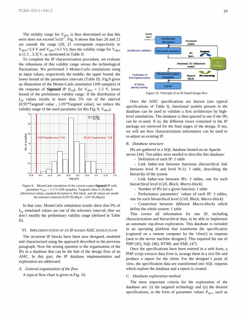
Figure 9. MonteCarlo simulation of the current output Sigmoid IP with
parameter Voffset = 1.5 V (100 samples). Targeted value is 20,40µA
(theoritical value), standard deviation is 304,34nA, and all values are inside
the tolerance interval [0,95*20,40µA ; 1,05*20,40µA].
In that case, MonteCarlo simulation results show that 0% of
Isig simulated values are out of the tolerance interval; thus we
don’t modify the preliminary validity range (defined in Table
II).
VI. IMPLEMENTATION OF AN IP-BASED ASIC DESIGN FLOW
The recurrent IP blocks have been now designed, modeled
and characterized using the approach described in the previous
paragraph. Now the arising question is the organization of the
IPs in a database that can be the hub of the design flow of an
ASIC. In this part, the IP database implementation and
exploration are addressed.
A. General organization of the flow
A typical flow chart is given in Fig. 10.
Architecture
description
IP
Database
IP
Database
System
specs
Mixed-level system
simulation
Functional simulation
Layout
IPs
Specs
Requests
Functional / IO / Behavioral
models
IPs recovering
Functional
models
Physical
blocks
Architecture validation
Verification of
final implementation
IP blocks
placing /routing
Architecture
description
IP
Database
IP
Database
System
specs
Mixed-level system
simulation
Functional simulation
Layout
IPs
Specs
RequestsIPs
Specs
RequestsRequestsRequests
Functional / IO / Behavioral
models
IPs recovering
Functional / IO / Behavioral
models
IPs recoveringIPs recoveringIPs recovering
Functional
models
Functional
models
Physical
blocks
Physical
blocks
Architecture validation
Verification of
final implementation
IP blocks
placing /routing
Figure 10. Principle of an IP-based design flow
Once the ASIC specifications are known (see typical
specifications of Table I), functional models present in the
database can be used to validate a first architecture by high-
level simulations. The database is then queried to see if the IPs
can be re-used. If so, the different views contained in the IP
package are retrieved for the final stages of the design. If not,
we will see how characterization information can be used to
re-adjust an existing IP.
B. Database structure
IPs are gathered in a SQL database hosted on an Apache
server [44]. Ten tables were needed to describe this database:
- Definition of each IP: 1 table
- Link father-son between functions (hierarchical link
between level N and level N-1): 1 table, describing the
hierarchy of the system
- Link father-son between IPs: 3 tables, one for each
hierarchical level (Cell, Block, Macro-block)
- Number of IPs for a given function: 1 table
- Performance parameters’ values of each IP: 3 tables,
one for each hierarchical level (Cell, Block, Macro-block)
- Connection between different Macro-blocks which
define the whole system: 1 table
This covers all information for one IP, including
characterization and hierarchical data, to be able to implement
an automatic top-down exploration. This database is included
in an operating platform that transforms the specification
(captured on a remote computer by the 'client') in requests
(sent to the server machine designer). This required the use of
PHP [45], SQL [46], HTML and XML [47].
Once the specifications have been entered in a web form, a
PHP script extracts data from it, arrange them in a text file and
produce a report for the client. For the designer’s point of
view, the specification data are transformed into SQL requests
which explore the database and a report is created.
C. Database exploration method
The most important criteria for the exploration of the
database are: (i) the targeted technology and (ii) the desired
specifications, in the form of parameter values Pspec, such as

TCAD-2011-0412
11
those of Table I: Voffset, Kslope, τ, Vequi, gmax. As explained
previously, re-usability of each of the IP is characterized by
validity domains [Pmin , Pmax] for the performance parameters
Voffset, Kslope, Vequi, gmax. For the kinetics parameter, τ, it
depends on an external capacitance value, connected to the
kinetic block.
The exploration method is a Top-Down one, from the
Macro-Block Level to the Cell Level; an IP is selected if its
performance validity domains can cover the targeted
specifications, i.e. if :
Pmin < Pspec < Pmax (6)
The database exploration algorithm is based on the principle
illustrated by the chart of Fig. 11. If we have different
corresponding IPs, we take the closest to the specifications: we
calculate, for each parameter, the distance between the
specification and the middle of the validity range, named d:
2
minmax PPPd spec
(7)
Then we accumulate the total distance by adding the
contribution of each parameter. It is logical to take the IP
corresponding to the minimum total distance.
Figure 11. Exploration algorithm used to look for an IP in the database
D. Results of the exploration
As illustrated on Fig. 11, when looking for one IP
corresponding to given specifications, the answer can be:
- a) one IP exists in the database
- b) no IP could be immediately found but there is one IP
whose performances are close to the specifications
- c) one IP corresponds to the specifications but it was
designed in another technology process.
In case a), the IP package is recovered by the designer. In
cases b) and c), an aid for re-design is given. Case b) will be
illustrated in an example in the next part. In the case (c)) the
issue results from the technology or the supply voltage, some
guidelines we developed for a resizing methodology can help
to fix the problem, [48] but that will not be detailed here.
At the final step, a diagnosis is returned and quantifies the
possibility of re-using IPs for a new ASIC project. This is
illustrated in Fig. 12. In practice, this step is performed thanks
to an XML file that summarizes the results of the exploration
and allows generating an HTML page (not shown) of the
diagnosis. In case of a successful exploration (previous case
a)), this page also indicates, the result of the automatic
calculation of external capacitances (needed to obtain the
desired values) and details the IP content with related links to
access more information.

TCAD-2011-0412
12
Figure 12. Screen snapshot of HTML diagnosis of re-use for a given ASIC design project ; a green boxt means “the IP has been found with the desired
specfications”, a red box means “no IP has been found” and a white box reports on a case not applicable. This diagnosis describes firstly the connection status to
the database, the number of requested neurons, the chosen technology and associated supply voltage. Secondly, it describes the result of the top-down database
exploration. We see in the example that the macro-block FS neuron didn’t match all the specifications. Tests to identify the problem source showed that the
Sodium current blocks didn’t match and more specifically the Sigmoid Cells. The problematic parameter is then Vslope_inactivation, as the exploration algorithm
cannot find a corresponding IP. A table summarizes the results: green marks when the IP is identified, red mark otherwise.
VII. EXAMPLES OF USE
The database automatic exploration process has been tested
on many plausible specifications’ sets. Here we propose two
examples of the implemented design flow, each one
corresponding to realistic design projects.
A. Design project 1
For this first application, the objective is to design one
neuromorphic ASIC, which is composed of five neurons: three
are regular spiking neurons (RS neuron), one is a fast spiking
neuron (FS neuron) and one is a slow conductance neuron (5c
neuron) [49]. The initial specifications, defined in agreement
with our biologist partners, are partially given on Table I of
part III. This Table summarizes the specifications of 2 of the 5
neurons.
As biological specifications are filled in, designer chooses
conversion factors (voltage and capacitance factors) as well as
the targeted technology to transform biological specifications
to electrical specifications.
In this favourable case of use, the diagnosis of re-use
indicates a total success, i.e. all needed IPs have been found in
the database. The exploration program takes less than one
minute to give the result, in the form of 5 diagnosis tables.
Then, the designer can quickly retrieve the system netlist, as
well as all IP-packages. At this step, the designer is able to
perform different verifications through multi-level simulations
of the entire ASIC.

TCAD-2011-0412
13
Figure 13. Multi-level abstraction simulation results of one ASIC setting with
5 neurons
To illustrate this, Fig. 13 shows a multi-level simulation of
the full ASIC. We test the RS neuron 3 and 5c neuron with
transistor level descriptions (Schematic view) while the other
blocks use Behavioral views. The validation criterion is the
presence of oscillations with neuromimetic spikes on the
membrane voltage of each neuron, what appears clearly on the
transient response. The Behavioral view realizes a
compromise between accuracy and computation time. The
simulation of one FS neuron at transistor level takes 14 min
56 s for a simulation stop time of 60 ms; this duration
decreases to 3 min 17 s using the Behavioral view.
Furthermore, this simulation time increases exponentially
versus the number of neurons (around 10 hours for a
simulation of 5 neurons at transistor level). This design
project 1 was complete and was sent to the foundry. This new
ASIC named Galway is currently working.
B. Design project 2
For this second application, the objective is to design one
ASIC composed of two neurons. The initial specifications are
slightly different from those of Table I; the specification for
Vslope_inact for Na conductance is now - 23 mV instead of -7.3
mV (both values are biologically realistic). Fig. 12 represents
the diagnosis of re-use for this new set of specifications. It
indicates that the specifications of the inactivation sigmoid IP
of Sodium current of a Neuron 1 could not be met during the
exploration (presence of the red rectangle in the table). At this
step, the designer has localized the issue and our tool includes
an aid for re-design. The idea is to create a new IP block by re-
sing an existing one.
First of all, the database is re-explored for finding the
sigmoid IP that is the closest to the required specifications.
This can be performed simply and automatically by
minimizing the distance defined by equation (6).
In the current example, the problem comes from the
specification of the Vslope parameter. The sizing relation
between Vslope and the design parameters, which has been
expressed previously in equation (5), can be found in the
Documentation file of the sigmoid IP.
To adequately re-size the IP, we just have to change the
value of one design parameter, R. In our case, we changed the
value from 30 kΩ to 35 kΩ, which had the consequence to
shift the Vslope validity domain to include the specification
value. The layout view has to be redesigned from the original
one. Usually it just consists in enlarging or reducing the size of
resistances or capacitors. Nevertheless, in some case, it could
be more complex and require the use of automatic layout
resizing techniques [25], [50]. This new IP can now be added
to the database. Its design time is almost negligible compared
to the first-time design of one IP. Thanks to the documentation
view, that expresses the relationships between the design
parameters and the performance parameters, re-sizing just
consists in modifying the design parameters.
VIII. CONCLUSION
Globally, automation of the analog design process is still an
open challenge, and re-use methodology is a predominant
recommendation of the ITRS. This paper has proposed a
synthesis of an experience in analog IC design, centered on the
notion of IP. Following the presentation of the issue and
review of contributions found in the literature, a methodology
is explained in details, with a tutorial intention.
In order to develop an analog design flow based on re-use,
some preliminary work is necessary: it includes a clear
definition of the system hierarchy, and the identification of the
the computation primitives, or IP blocks, at each level of the
hierarchy. IP blocks of the lowest level include several
transistors and each one is associated with a function. We
applied our methodology to the case of neuromimetic ASICs,
which design needs can be addressed by our design flow.
Furthermore, these devices offer a clear definition of design
primitives and system hierarchy.
The starting point of the methodology was an existing
library of Hard IP blocks and the first question addressed here
is: what information must be added to a Hard IP to transform it
into a Firm IP? The proposed answer is (i) to develop a set of
models, adapted to multiple abstraction levels, (ii) to formulate
the sizing relationships between performance parameters and
design parameters and (iii) to characterize to what extent the
IP can keep its functionality, when varying the values of
performances parameters.
The next point is the implementation of an ASIC design

TCAD-2011-0412
14
flow centered on a database gathering these IPs. A SQL
database, including IP packages and hierarchical links between
blocks, has been built that allows the implementation of an
automatic top-down exploration. We explained the algorithm
used to found an IP corresponding to the desired
specifications. Finally, the resulting automatic design flow has
been tested for two plausible ASIC design projects. These
examples show how our web-based platform can assist the
designer: it globally accelerates the system design cycle, the
designer can quickly see a diagnosis of re-use for his targeted
ASIC. In case of total success, the IP packages are
immediately retrieved and the designer can perform multi-level
simulations of the entire ASIC in a verification phase; in case
of partial success, our tool proposes an aid to re-design an IP
that matches the specifications.
REFERENCES
[1] R. Saleh, S. Wilton, S. Mirabbasi, A. Hu, M. Greenstreet, G. Lemieux, P. P. Pande, C. Grecu, and A. Ivanov, “System-on-Chip: Reuse and Integration”, Proceedings of the IEEE, vol. 94, n°. 6, pp. 1050 - 1069, June 2006
[2] M. Keating and P. Bricaud, Reuse methodology manual, 2nd edition ed., Kluwer Academic Publishers, 1999
[3] International Technology Roadmap for Semiconductors (ITRS), Design, Edition 2009
[4] J. Tomas, Y. Bornat, S. Saighi, T. Levi and S. Renaud, “Design of a modular and mixed neuromimetic ASIC”, Proceedings ICECS 2006, pp. 946-949, Nice, France, December 2006
[5] T. Levi, N. Lewis, S. Saighi, J. Tomas, Y. Bornat and S. Renaud, “Neuromimetic Integrated Circuits”, Chap. 12 in VLSI Circuits for Biomedical Applications, Artech House, Boston, pp. 241-264, 2008
[6] S. Saighi, Y. Bornat, J. Tomas, G. Le Masson and S. Renaud, “A Library of Analog Operators Based on the Hodgkin-Huxley Formalism for the Design of Tunable Real-Time Silicon Neurons”, IEEE Transactions on Biomedical Circuits and Systems, vol. 5, pp. 3-19, February 2011
[7] A. Basu, S. Brink, C. Schlottmann, S. Ramakrishnan, C. Petre, S. Koziol, F. Baskaya, C. Twigg and P. Hasler, “A Floating-Gate-Based Field-Programmable Analog Array”, IEEE Journal of Solid-State Circuits, vol. 45, n°. 9, pp. 1781-1794, September 2010
[8] H. Koh, C. Sequin and P. Gray, “OPASYN: a compiler for CMOS operational amplifiers”, IEEE Transactions on Computer-Aided Design of Integrated Circuits and Systems, vol. 9, pp. 113-125, February 1990
[9] R. Phelps, M. Krasnicki, R. Rutenbar, L. Carley and J. Hellums, “Anaconda: simulation-based synthesis of analog circuits via stochastic pattern search”, IEEE Transactions on Computer-Aided Design of Integrated Circuits and Systems, vol. 19, pp. 703-717, June 2000
[10] R. Iskander, Knowledge-aware synthesis for analog integrated circuit design and reuse, Dissertation, University Pierre et Marie Curie, Paris VI, July 2008
[11] E. Martens and G. Gielen, High-level modeling and synthesis of analog integrated systems, Springer, January 2008
[12] R. Harjani, R. Rutenbar, and L. R. Carley, “OASYS: A framework for analog circuit synthesis”, IEEE Transactions on Computer-Aided Design, vol. 8, no. 12, pp. 1247–1265, December 1989
[13] R. Rutenbar, G. Gielen and J. Roychowdhury, “Hierarchical Modeling, Optimization, and Synthesis for System-Level Analog and RF Designs”, Proceedings of the IEEE, vol. 95, n°. 3, March 2007
[14] P. Nguyen Tuong, Définition et implantation d’un langage de conception de composants analogiques réutilisables, Dissertation, University Pierre et Marie Curie, Paris VI, June 2006
[15] H. Chang, E. Charbon, U. Choudhury, A. Demir, E. Felt, E. Liu, E. Malavasi, A. Sangiovanni-Vincentelli, and I. Vassiliou, A Top-Down, constraint-Driven Design Methodology for Analog Integrated Circuits, Boston, MA: Kluwer, 1997
[16] G. Gielen, R. Rutenbar, “Computer-aided design of analog and mixed-signal integrated circuits”, in Proceedings of the IEEE, vol. 88, no. 12, pp. 1825-1852, December 2000
[17] R. Castro-Lopez, F.V. Fernandez, O. Guerra-Vinuesa and A. Rodriguez-Vasquez, Reuse-Based Methodologies and Tools in the Design of Analog and Mixed-Signal Integrated Circuits, Springer Publishers, 2006
[18] F. De Bernardinis, P. Nuzzo and A.S. Vincentelli, “Robust System Level Design with Analog Platforms”, Proceedings Computer-Aided Design ICCAD'06, pp. 334-341, San Jose, US, November 2006
[19] X. Sun, P. Nuzzo, C-C. Wu and A.S. Vincentelli, “Contract-Based System-Level Composition of Analog Circuits”, Proceedings ACM/IEEE Design Automation Conference, pp. 605-610, San Francisco, US, July 2009
[20] S. Ohr and L. Marchant, “PANEL : analog intellectual property : now ? or never ?”, Proceedings ACM/IEEE Design Automation Conference, pp. 181-182, New Orleans, US, June 2002
[21] R.J. Koch and F. Dielacher, “Analog IP – stairway to SoC heaven ?”, Proceedings IEEE Solid-State Circuits Conference, pp. 1-2, San Francisco, US, February 2003
[22] R. Singh, “Analog IP re-use: concerns for “digitally-oriented” SoC designers”, EETIMES 19/12/2005
[23] R. Goering, “True Circuits rolls out 65-nm analog IP”, EETIMES 12/06/2006
[24] Z. Li, L. Luo and J. Yuan, “A Study on Analog IP Blocks for Mixed-Signal SoC”, Proceedings ASIC, pp.564-567, Beijing, China, October 2003
[25] M. Dessouky, A. Kaiser, M-M. Louërat and A. Greiner, “Analog Design for Reuse – Case Study : Very Low-voltage ∆Σ Modulator”, Proceedings DATE 2000, pp. 353–360, Paris, France, March 2000
[26] B. Gilbert, Design for manufacture, Trade-offs in analog circuit design. The designer’s companion, Kluwer Academic Publishers, 2002
[27] VSIA, “Analog/Mixed-Signal VSI Extension Specification Version 2.2”, http://vsi.org/docs/AMS-122-26Feb01.pdf.
[28] J. Michel and F. Schwartz, “Analogue circuit sizing method using interval analysis”, Proceedings of the 2008 Joint International IEEE Northeast Workshop on Circuits and Systems and TAISA Conference, NEWCAS-TAISA, pp. 331-334, Montreal, Canada, 2008.
[29] I. O’Connor, F. Tissafi-Drissi, G. Révy and F. Gaffiot, “UML/XML-based approach to hierarchical AMS synthesis”, Proceedings FDL 2005, Lausanne, Switzerland, September 2005
[30] I. O'Connor and al., “CNTFET Modeling and Reconfigurable Logic-Circuit Design”, IEEE Transactions on Circuits and Systems I, vol. 54, pp. 2365-2379, November 2007
[31] I. Connor and A. Kaiser, “Automated synthesis of current-memory cells”, IEEE Transactions on Computer-aided Deign of. Integrated Circuits Systems, vol. 19, no. 4, pp. 413-424, April 2000
[32] R. Castro-Lopez, O. Guerra, E. Roca and F.V. Fernandez, “An Integrated Layout-Synthesis Approach for Analog ICs”, IEEE Transactions on Computer-aided Design of Integrated Circuits and Systems, vol. 27, pp. 1179-1189, July 2008
[33] Hamour, M.; Saleh, R.; Mirabbasi and S.; Ivanov, “Analog IP design flow for SoC applications”, Proceedings ISCAS 2003, vol. 4, pp. 676-679, Bangkok, Thailand, May 2003
[34] J.V.B. Pimentel and J.C. Da Costa, “A Methodology for Describing Analog/Mixed-Signal Blocks as IP”, Design&Reuse Articles, November 2010
[35] D. M. Binkley, C. E. Hopper, S. D. Tucker, B. C. Moss, J. M. Rochelle and D. P. Foty, “A CAD Methodology for Optimizing Transistor Current and Sizing in Analog CMOS Design”, IEEE Transactions on Computer-aided Design of Integrated Circuits and Systems, vol. 22, pp. 225-237, February 2003
TCAD-2011-0412
15
[36] R. Iskander, L. de Lamarre, A. Kaiser and M.-M. Rosset-Louërat, “Design Space Exploration for Analog IPs using CAIRO+”, ICEEC International Conference on Electrical Electronic and Computer Engineering , pp. 473-476, Cairo, Egypt, 2004
[37] R. Iskander, M.-M. Louërat and A. Kaiser, “Automatic DC Operating Point Computation and Design Plan Generation for Analog IPs”, Analog Integrated Circuit and Signal Processing Journal, vol. 56, 2008
[38] F. Tissafi-Drissi, I. O'Connor, and F. Gaffiot, “RUNE: Platform for automated design of integrated multi-domain systems. Application to high-speed CMOS photoreceiver front-ends”, Proceedings of the IEEE Conference on Design Automation and Test in Europe, DATE'04, pp. 16-21, Paris, 2004
[39] A.L. Hodgkin and A.F. Huxley, “A quantitative description of membrane current and its application to conduction and excitation in nerve”, Journal of Physiology, 1952
[40] S. Renaud, J. Tomas, N. Lewis, Y. Bornat, A. Daouzli, M. Rudolph , A. Destexhe and S. Saighi, “PAX: A mixed hardware/software simulation platform for spiking neural networks”, Journal of Neural Networks, vol. 23, pp. 905-916, April 2010
[41] Verilog-A, Language Reference Manual, Cadence, August 1996
[42] C. J. R. Shi and A. Vachoux, “VHDL-A design objectives and rationale”, in Current issues in electronic modeling. vol. 2, K. A. Publishers, pp. 1-30, 1995
[43] F. Pêcheux, C. Lallement and A. Vachoux, “VHDL-AMS and Verilog-AMS as Alternative Hardware Description Languages for Efficient Modeling of Multidiscipline Systems”, IEEE Transactions on Computer-Aided Design of Integrated Circuits and Systems, vol. 24, February 2005
[44] R. Bowen, K. Coar, Apache server, Campus Press, 2000
[45] P.Rigaux, Pratique de MySql et Php, O’Reilly, 2006
[46] P. Dubois, MySQL, Sams Developer's Library, 2005
[47] S. Abiteboul, P. Buneman, D. Suciu, Data on the web from relations to semistructured data and XML, Morgan Kaufmann Publishers, 2000
[48] T. Levi, J. Tomas, N. Lewis, P. Fouillat, “A CMOS Resizing Methodology for Analog Circuits: linear and non-linear applications”, IEEE Journal Design and Test of Computer, vol. 26, pp. 78-87, January-february 2009
[49] S. Renaud, J. Tomas, Y. Bornat, A. Daouzli, S. Saïghi, “Neuromimetic ICs with analog cores: an alternative for simulating spiking neural networks”, Proceedings ISCAS 2007, pp 3355-3358, New-Orleans, USA, May 2007
[50] S. Youssef, F. Javid, D. Dupuis, R. Iskander, M. Louerat, “A Python-based layout-aware analog design methodology for nanometric technologies”, IEEE Design and Test Workshop, pp. 62-67, Beirut, Lebanon, December 2011
Dr. Timothée Levi was born in Talence, France in 1981. He received the
Engineer degree in electronics from Electronic Engineering School of
Bordeaux (ENSEIRB-MATMECA) and the Master degree in electronics from
the University of Bordeaux 1, France in 2004. He received the Ph.D. degree
in Electrical, from the University of Bordeaux 1 in 2007. His dissertation was
about the reuse methodology applied on neuromorphic engineering.
In 2008, he was a post-doctoral researcher at CEA-LETI in Grenoble,
France, about real-time signal processing of spike sorting. In 2009, he was
post-doctoral researcher at University of Tokyo (LIMMS / IIS), Japan, about
silicon neural network for smart MEMS systems.
He is currently Associate Professor at Laboratory IMS (CNRS/ENSEIRB,
University Bordeaux 1) since 2010. His main research is focused on
architecture of silicon neural networks and reuse methodologies. He authored
and co-authored 2 chapters of book, 6 journal articles, one patent and about
20 conference articles.
Dr. Noëlle Lewis holds a Ph.D. in Electronics from Bordeaux University,
France, in 1997 and she is associate professor since 2000 at IMS laboratory,
at Bordeaux University. Her first topic of interest was behavioral modeling of
analogue integrated circuits. She joined the “Engineering of Neuromorphic
Systems” (ISN) research team of IMS lab in 2005, to contribute to solve some
critical points related to analogue IC integration with IP re-use techniques.
Since 2010, she is the head of a new research team focusing on Electronic
Systems Interacting with Biology, ELIBIO, a research team in which 3
faculties, 3 Ph. D. students and 2 engineers are involved. Currently, this team
participates to 3 projects funded by the french National Research Agency and
covering new fields of specializations like: biomedical instrumentation, low
power low frequency IC for bio-signal recording, real-time low power signal
processing and closed-loop neural stimulation.
Dr. Jean Tomas received the M.Sc. degree in Electrical Engineering from
Ecole Nationale Supérieure d'Electronique et de Radioélectricité de Bordeaux
(ENSERB) in 1985 and the Ph.D. degree in Electrical Engineering from
Université Bordeaux 1 in 1988.
His research interests include design of analog and mixed signal circuits
and systems dedicated to neuromorphic applications. He has also authored
and co-authored more than 50 peer-review publications.
Currently, he is Associate Professor at Université Bordeaux 1 in IMS
Laboratory (UMR 5218 CNRS / Université de Bordeaux).
Pr. Sylvie Renaud graduated in electronic engineering (MSc) in Supelec
(Paris-France) in 1986. She received her PhD in Physics at the University of
Bordeaux (France) in 1990, and her HDR (Research Habilitation) in 2001.
After a post-doctoral stay at Brandeis University (MA, USA) in 1991_1992,
she was appointed as an Assistant-Professor, then Professor in ENSEIRB
Bordeaux (National Engineering School) where she was recently appointed as
Research Board Director in the Institut Polytechnique de Bordeaux.
She created in 1994 the « Engineering of Neuromorphic Systems » group
in IMS-Labs (Univ. Bordeaux, CNRS, ENSEIRB), and now heads the
BioElectronics group with 12 permanent researchers. Her research interests
are: analog and mixed neuromorphic VLSI; real-time hardware simulation
platforms of spiking neural networks; hybrid systems interfacing living and
artificial neurons; analog ASICs for biological signal conditioning and events
detection; active VLSI implants for neurodegenerative diseases and diabetes;
closed-loop living-artificial systems. She authored and co-authored more than
50 reviewed international articles and communications.
Prof Renaud is an expert for the EU commission on FET and ICT calls,
and for NS-NIH on CRCNS calls. She is a reviewer for IEEE journals and
conferences since 1997 and organizes special Sessions, Tutorials and
workshops in IEEE conferences on a regular basis.