application noteapplication note
TRANSCRIPT

JB, 2009-06-23 Page 1 of 9
A p p l i c a t i o n N o t eA p p l i c a t i o n N o t eA p p l i c a t i o n N o t eA p p l i c a t i o n N o t e
The The The The Protection of USB Protection of USB Protection of USB Protection of USB 2.0 2.0 2.0 2.0 Applications Applications Applications Applications
USBUSBUSBUSB Port ProtectionPort ProtectionPort ProtectionPort Protection
The USB-Interface might be the most distributed PC interface in the world. The usage in industry-
applications is more and more common. Let’s have a closer look to the special environmental conditions of
industry applications.
That there are real concerns regarding the robustness against EMI and ESD is written in Intel’s “High Speed
USB Platform Design Guidelines”. Intel recommends the usage of a common mode choke for EMI
suppressions and another component for protection against ESD pulses.
Würth Elektronik offers all these types of products.
- The WE-CNSW common mode choke was developed for EMI suppression on high speed signal
lines
- For ESD suppression the TVS diode arrays WE-TVS with very low capacitances (<2pF) or the ESD
Suppressors WE-VE (capacitances down to 0.05pF) are your preferred choice.
But for outstanding EMI behaviour it is absolutely necessary to protect the power supply (Vbus) as well. A lot
of design engineers forget this important point and wonder themselves when their product don’t pass all
the tests in EMI lab.
Two typical schematics for optimized protection of one or two USB ports are shown below:
With one TVS diode array WE-TVS you can fully
protect two USB lines. All four signal lines as well
as the common power supply are well protected.
For further optimization, i.e. to filter incoming
common mode noise as well as differential mode
noise from USB line, a LC filter is built with the
common mode choke WE-CNSW and the
capacitors.
For power supply lines very good noise
suppressions can be reached with a chip bead
ferrite, like the Würth Elektronik WE-CBF series.
Single line protection components like ESD
suppressors series WE-VE also have to be
connected from signal line to GND. For power
line protection it is not necessary to use a low
cap ESD suppressor, you might prefer a
standard SMD varistor which can withstand
higher surges and higher transient energies.
JB, 2009-06-23 Page 2 of 9
A p p l i c a t i o n N o t eA p p l i c a t i o n N o t eA p p l i c a t i o n N o t eA p p l i c a t i o n N o t e
The The The The Protection of USB Protection of USB Protection of USB Protection of USB 2.0 2.0 2.0 2.0 Applications Applications Applications Applications
About TVS About TVS About TVS About TVS DDDDiodesiodesiodesiodes
Würth Elektronik launched the TVS diodes array series called WE-TVS. These TVS diodes arrays include
three main functions:
- protection against ESD pulses according to EN 61000-4-2
- protection against surge pulses according to EN 61000-4-5
- protection against EFT pulses according to EN 61000-4-4
WE-TVS series are high performance designed TVS diode arrays which include surge rated diodes. They
are the best choice to protect high speed data lines like USB 2.0, DVI or LAN from over-voltages. The WE-
TVS series exceeds the requirements outlined in EN 61000-4-2. Due to their ultra low capacitance (<2.0 pF)
they are nearly invisible on the signal lines.
AboAboAboAbout ESD Suppressorsut ESD Suppressorsut ESD Suppressorsut ESD Suppressors
The ESD suppressors are special raised varistors with a low and defined intrinsic capacitance. Würth
Elektronik has three different series:
- WE-VE standard series: Capacitances of 1pF to 120pF and voltages from 5V to 24V
- WE-VE “ULC” series: Capacitance of 0.2pF, suitable for signal lines up to 12V
- WE-VE femtoF series: Capacitance of 0.05pF and rated voltages of 6V, 14V and 26V
For the first two series are also four-fold array packages available.
Why ESDWhy ESDWhy ESDWhy ESD Protection?Protection?Protection?Protection?
Since the first electronic developments, all the parts are subjected to electrostatic discharge. ESD events
have peak voltages up to 30kV and therewith they are very dangerous for all kind of integrated circuits.
However, some state-of-the-art ICs are protected against ESD pulses but real world conditions show daily
that an additional protection device is indispensable. On the one hand to have the whole board ESD free
and on the other hand to develop more reliable products to satisfy the needs of your customers.
Why EMIWhy EMIWhy EMIWhy EMI Suppres Suppres Suppres Suppressionsionsionsion????
With the increase in electronic/electrical products and the need to have wireless connectivity in today’s
global markets, there is an increased requirement to ensure that your product is immune to the impacts
caused by both the intentional and un-intentional RF environment. Only if you consider now which EMI
phenomena impacts on the product, will you be able to design in the appropriate protection and reduce
time to market.
In addition, the product must not generate excessive levels of EMI and this is typically assessed by an EMC
Test Laboratory, and should the product fail then costs to implement remedial work will increase
aggressively.
JB, 2009-06-23 Page 3 of 9
A p p l i c a t i o n N o t eA p p l i c a t i o n N o t eA p p l i c a t i o n N o t eA p p l i c a t i o n N o t e
The The The The Protection of USB Protection of USB Protection of USB Protection of USB 2.0 2.0 2.0 2.0 Applications Applications Applications Applications
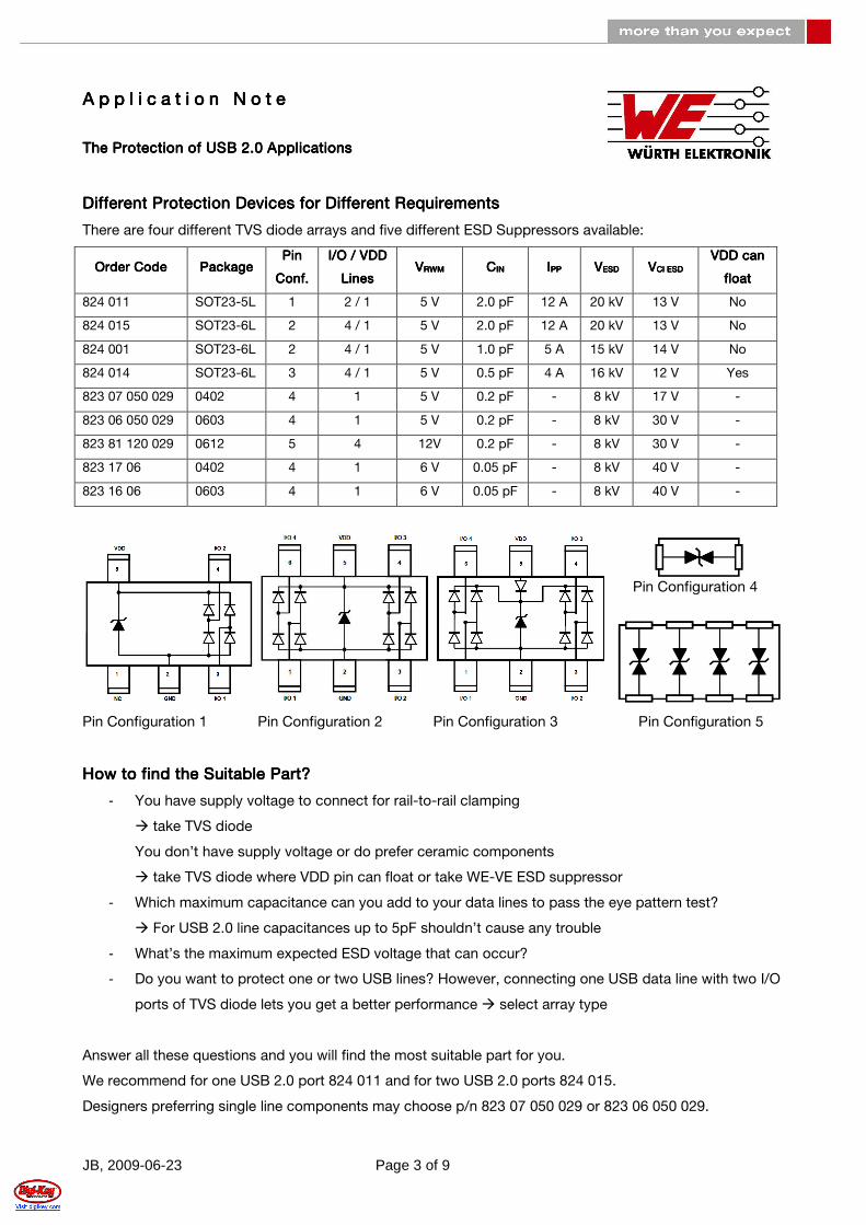
Different Different Different Different Protection DevicesProtection DevicesProtection DevicesProtection Devices forforforfor Different Requirements Different Requirements Different Requirements Different Requirements
There are four different TVS diode arrays and five different ESD Suppressors available:
Order CodeOrder CodeOrder CodeOrder Code PackagePackagePackagePackage Pin Pin Pin Pin
Conf.Conf.Conf.Conf.
IIII////OOOO //// VDDVDDVDDVDD
LinesLinesLinesLines VVVVRWMRWMRWMRWM CCCC ININININ IIIIPPPPPPPP VVVVESDESDESDESD VVVVCl Cl Cl Cl ESDESDESDESD
VDD VDD VDD VDD can can can can
floatfloatfloatfloat
824 011 SOT23-5L 1 2 / 1 5 V 2.0 pF 12 A 20 kV 13 V No
824 015 SOT23-6L 2 4 / 1 5 V 2.0 pF 12 A 20 kV 13 V No
824 001 SOT23-6L 2 4 / 1 5 V 1.0 pF 5 A 15 kV 14 V No
824 014 SOT23-6L 3 4 / 1 5 V 0.5 pF 4 A 16 kV 12 V Yes
823 07 050 029 0402 4 1 5 V 0.2 pF - 8 kV 17 V -
823 06 050 029 0603 4 1 5 V 0.2 pF - 8 kV 30 V -
823 81 120 029 0612 5 4 12V 0.2 pF - 8 kV 30 V -
823 17 06 0402 4 1 6 V 0.05 pF - 8 kV 40 V -
823 16 06 0603 4 1 6 V 0.05 pF - 8 kV 40 V -
Pin Configuration 1 Pin Configuration 2 Pin Configuration 3 Pin Configuration 5
How to How to How to How to ffffind the ind the ind the ind the SSSSuitable uitable uitable uitable PPPPart?art?art?art?
- You have supply voltage to connect for rail-to-rail clamping
take TVS diode
You don’t have supply voltage or do prefer ceramic components
take TVS diode where VDD pin can float or take WE-VE ESD suppressor
- Which maximum capacitance can you add to your data lines to pass the eye pattern test?
For USB 2.0 line capacitances up to 5pF shouldn’t cause any trouble
- What’s the maximum expected ESD voltage that can occur?
- Do you want to protect one or two USB lines? However, connecting one USB data line with two I/O
ports of TVS diode lets you get a better performance select array type
Answer all these questions and you will find the most suitable part for you.
We recommend for one USB 2.0 port 824 011 and for two USB 2.0 ports 824 015.
Designers preferring single line components may choose p/n 823 07 050 029 or 823 06 050 029.
Pin Configuration 4
JB, 2009-06-23 Page 4 of 9
A p p l i c a t i o n N o t eA p p l i c a t i o n N o t eA p p l i c a t i o n N o t eA p p l i c a t i o n N o t e
The The The The Protection of USB Protection of USB Protection of USB Protection of USB 2.0 2.0 2.0 2.0 Applications Applications Applications Applications
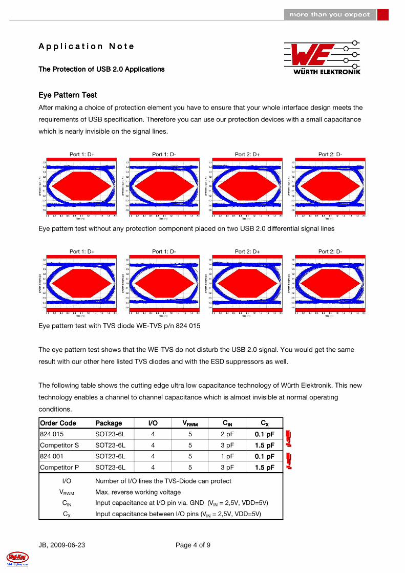
Eye PEye PEye PEye Pattern Tesattern Tesattern Tesattern Testttt
After making a choice of protection element you have to ensure that your whole interface design meets the
requirements of USB specification. Therefore you can use our protection devices with a small capacitance
which is nearly invisible on the signal lines.
Port 1: D+ Port 1: D- Port 2: D+ Port 2: D-
Eye pattern test without any protection component placed on two USB 2.0 differential signal lines
Port 1: D+ Port 1: D- Port 2: D+ Port 2: D-
Eye pattern test with TVS diode WE-TVS p/n 824 015
The eye pattern test shows that the WE-TVS do not disturb the USB 2.0 signal. You would get the same
result with our other here listed TVS diodes and with the ESD suppressors as well.
The following table shows the cutting edge ultra low capacitance technology of Würth Elektronik. This new
technology enables a channel to channel capacitance which is almost invisible at normal operating
conditions.
Order CodeOrder CodeOrder CodeOrder Code PackagePackagePackagePackage I/OI/OI/OI/O VVVVRWMRWMRWMRWM CCCCININININ CCCCXXXX
824 015 SOT23-6L 4 5 2 pF 0.1 pF0.1 pF0.1 pF0.1 pF
Competitor S SOT23-6L 4 5 3 pF 1.5 pF1.5 pF1.5 pF1.5 pF
824 001 SOT23-6L 4 5 1 pF 0.1 pF0.1 pF0.1 pF0.1 pF
Competitor P SOT23-6L 4 5 3 pF 1.5 pF1.5 pF1.5 pF1.5 pF
I/O Number of I/O lines the TVS-Diode can protect
VRWM Max. reverse working voltage
CIN Input capacitance at I/O pin via. GND (VIN = 2,5V, VDD=5V)
CX Input capacitance between I/O pins (VIN = 2,5V, VDD=5V)
JB, 2009-06-23 Page 5 of 9
A p p l i c a t i o n N o t eA p p l i c a t i o n N o t eA p p l i c a t i o n N o t eA p p l i c a t i o n N o t e
The The The The Protection of USB Protection of USB Protection of USB Protection of USB 2.0 2.0 2.0 2.0 Applications Applications Applications Applications
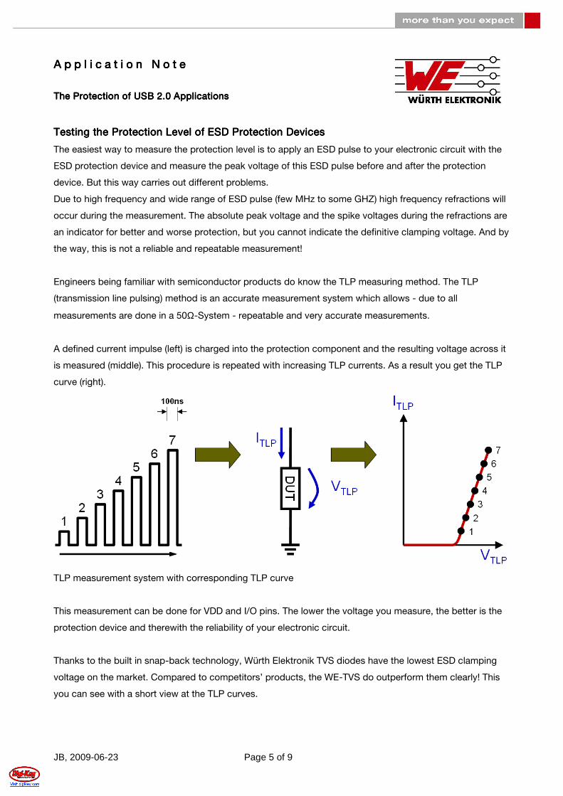
Testing the Protection Level of Testing the Protection Level of Testing the Protection Level of Testing the Protection Level of ESD Protection DevicesESD Protection DevicesESD Protection DevicesESD Protection Devices
The easiest way to measure the protection level is to apply an ESD pulse to your electronic circuit with the
ESD protection device and measure the peak voltage of this ESD pulse before and after the protection
device. But this way carries out different problems.
Due to high frequency and wide range of ESD pulse (few MHz to some GHZ) high frequency refractions will
occur during the measurement. The absolute peak voltage and the spike voltages during the refractions are
an indicator for better and worse protection, but you cannot indicate the definitive clamping voltage. And by
the way, this is not a reliable and repeatable measurement!
Engineers being familiar with semiconductor products do know the TLP measuring method. The TLP
(transmission line pulsing) method is an accurate measurement system which allows - due to all
measurements are done in a 50Ω-System - repeatable and very accurate measurements.
A defined current impulse (left) is charged into the protection component and the resulting voltage across it
is measured (middle). This procedure is repeated with increasing TLP currents. As a result you get the TLP
curve (right).
TLP measurement system with corresponding TLP curve
This measurement can be done for VDD and I/O pins. The lower the voltage you measure, the better is the
protection device and therewith the reliability of your electronic circuit.
Thanks to the built in snap-back technology, Würth Elektronik TVS diodes have the lowest ESD clamping
voltage on the market. Compared to competitors’ products, the WE-TVS do outperform them clearly! This
you can see with a short view at the TLP curves.

JB, 2009-06-23 Page 6 of 9
A p p l i c a t i o n N o t eA p p l i c a t i o n N o t eA p p l i c a t i o n N o t eA p p l i c a t i o n N o t e
The The The The Protection of USB Protection of USB Protection of USB Protection of USB 2.0 2.0 2.0 2.0 Applications Applications Applications Applications
Order CodeOrder CodeOrder CodeOrder Code PackagePackagePackagePackage I/OI/OI/OI/O VVVVRWMRWMRWMRWM VVVVCl,IOCl,IOCl,IOCl,IO VVVVCl,VDDCl,VDDCl,VDDCl,VDD VVVVESDESDESDESD CCCC ININININ IIIIPPPPPPPP
824 015 SOT23-6L 4 5 12121212 7,57,57,57,5 12 kV 2 pF 12 A
Competitor S SOT23-6L 4 5 22222222 15,515,515,515,5 15 kV 3 pF 12 A
824 001 SOT23-6L 4 5 14141414 9999 8 kV 1 pF 5 A
Competitor P SOT23-6L 4 5 28282828 19191919 8 kV 3 pF 6 A
I/O Number of I/O lines the TVS-Diode can protect
VRWM Max. reverse working voltage
VCl,IO ESD clamping voltage at I/O pin (IEC 61000-4-2, contact mode at 6kV)
VCl,VDD ESD clamping voltage at VDD pin (IEC 61000-4-2, contact mode at 6kV)
VESD Max. withstanding ESD pulse (IEC 61000-4-2, contact mode)
CIN Input capacitance at I/O pin via. GND (VIN = 2,5V, VDD=5V)
IPP Max. Withstanding surge current (8/20µs)
TLP Curve of different parts for VDD TLP Curve of different parts for I/O lines
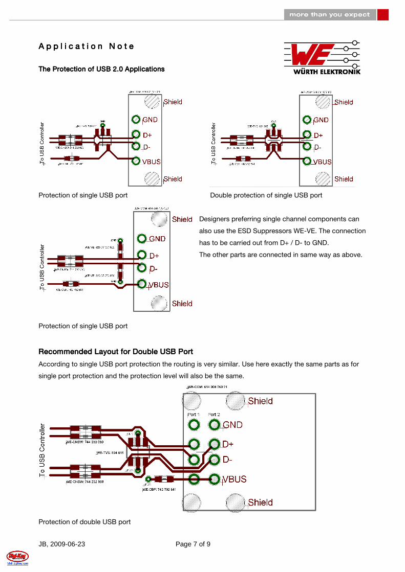
Recommended LayoutRecommended LayoutRecommended LayoutRecommended Layout for S for S for S for Single USB Portingle USB Portingle USB Portingle USB Port
The two differential signal lines (D+ and D-) are routed from connector to TVS-Diode (p/n 824 011) and via a
common mode choke (p/n 744 232 090) to the USB controller as shown on the left picture below. This
results in an awesome ESD protection and EMI suppression of both data lines.
VBUS is routed like the signal line, but instead of the common mode choke a chip bead ferrite
(p/n 742 792 641) is used. After the chip bead you may add a capacitor and a second chip bead as well to
get the highest possible EMI suppression effect.
For very sensible IC’s and / or high reliable applications you can get an optimized ESD suppression effect if
you double contact a four-fold TVS array (p/n 824 015) like shown on right picture.
JB, 2009-06-23 Page 7 of 9
A p p l i c a t i o n N o t eA p p l i c a t i o n N o t eA p p l i c a t i o n N o t eA p p l i c a t i o n N o t e
The The The The Protection of USB Protection of USB Protection of USB Protection of USB 2.0 2.0 2.0 2.0 Applications Applications Applications Applications
Protection of single USB port Double protection of single USB port
Designers preferring single channel components can
also use the ESD Suppressors WE-VE. The connection
has to be carried out from D+ / D- to GND.
The other parts are connected in same way as above.
Protection of single USB port
Recommended Layout Recommended Layout Recommended Layout Recommended Layout forforforfor DDDDouble USB Portouble USB Portouble USB Portouble USB Port
According to single USB port protection the routing is very similar. Use here exactly the same parts as for
single port protection and the protection level will also be the same.
Protection of double USB port
JB, 2009-06-23 Page 8 of 9
A p p l i c a t i o n N o t eA p p l i c a t i o n N o t eA p p l i c a t i o n N o t eA p p l i c a t i o n N o t e
The The The The Protection of USB Protection of USB Protection of USB Protection of USB 2.0 2.0 2.0 2.0 Applications Applications Applications Applications
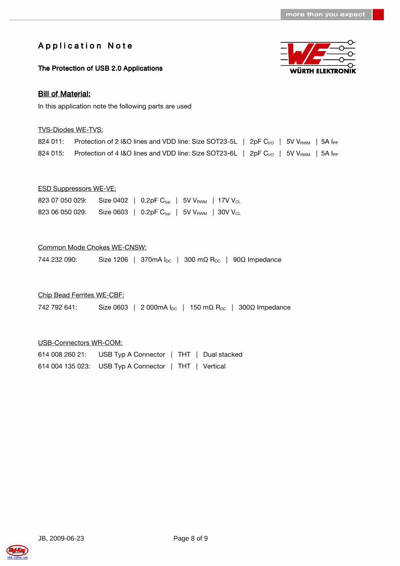
Bill of MaterialBill of MaterialBill of MaterialBill of Material::::
In this application note the following parts are used
TVS-Diodes WE-TVS:
824 011: Protection of 2 I&O lines and VDD line: Size SOT23-5L | 2pF CI/O | 5V VRWM | 5A IPP
824 015: Protection of 4 I&O lines and VDD line: Size SOT23-6L | 2pF CI/O | 5V VRWM | 5A IPP
ESD Suppressors WE-VE:
823 07 050 029: Size 0402 | 0.2pF Ctyp | 5V VRWM | 17V VCL
823 06 050 029: Size 0603 | 0.2pF Ctyp | 5V VRWM | 30V VCL
Common Mode Chokes WE-CNSW:
744 232 090: Size 1206 | 370mA IDC | 300 mΩ RDC | 90Ω Impedance
Chip Bead Ferrites WE-CBF:
742 792 641: Size 0603 | 2 000mA IDC | 150 mΩ RDC | 300Ω Impedance
USB-Connectors WR-COM:
614 008 260 21: USB Typ A Connector | THT | Dual stacked
614 004 135 023: USB Typ A Connector | THT | Vertical
JB, 2009-06-23 Page 9 of 9
A p p l i c a t i o n N o t eA p p l i c a t i o n N o t eA p p l i c a t i o n N o t eA p p l i c a t i o n N o t e
The The The The Protection of USB Protection of USB Protection of USB Protection of USB 2.0 2.0 2.0 2.0 Applications Applications Applications Applications
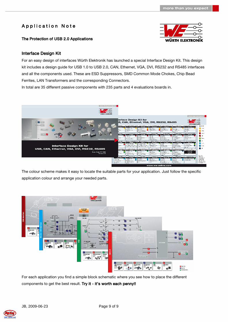
Interface Design KitInterface Design KitInterface Design KitInterface Design Kit
For an easy design of interfaces Würth Elektronik has launched a special Interface Design Kit. This design
kit includes a design guide for USB 1.0 to USB 2.0, CAN, Ethernet, VGA, DVI, RS232 and RS485 interfaces
and all the components used. These are ESD Suppressors, SMD Common Mode Chokes, Chip Bead
Ferrites, LAN Transformers and the corresponding Connectors.
In total are 35 different passive components with 235 parts and 4 evaluations boards in.
The colour scheme makes it easy to locate the suitable parts for your application. Just follow the specific
application colour and arrange your needed parts.
For each application you find a simple block schematic where you see how to place the different
components to get the best result. Try it Try it Try it Try it ---- it’s worth it’s worth it’s worth it’s worth each peneach peneach peneach pennynynyny!!!!!!!!