application note an-1170 audio power quad flat no-lead (pqfn
TRANSCRIPT

Audio PQFN Technology AN-1170 Board Mounting Application Note www.irf.com Version 5, June 2016 Page 1 of 14
Application Note AN-1170
Audio Power Quad Flat No-Lead (PQFN) Board Mounting Application Note
Table of Contents Page Device construction ................................................2 Design considerations ............................................3 Assembly considerations ........................................4 Mechanical test results ...........................................8 Appendix A Model-specific data .......................... 10 Appendix A.1 5x6 D devices ............................... 11 Appendix A.2 32-lead 7x7 devices ...................... 12 Appendix A.2 44-lead 7x7 devices ...................... 13
The PQFN package family comprises efficient devices with a wide range of input voltages, all of which are lead-free as indicated by the PbF suffix after the part number (for example, IRFH3800PbF). There are various sizes and outlines. The main text of this application note contains guidance applicable to the whole Audio range of PQFN devices, while Appendix A contains device outlines, substrate layouts and stencil designs for each device. For more detail about individual devices, refer to the relevant product data sheet and package outline drawing. To simplify board mounting and improve reliability, International Rectifier manufactures PQFN devices to exacting standards. These high standards have evolved through evaluating many different materials and designs. Although such evaluations have yielded good results, the recommendations in this application note may need to be adjusted to suit specific production environments.

Audio PQFN Technology AN-1170 Board Mounting Application Note www.irf.com Version 5, June 2016 Page 2 of 14
Introduction Power Quad Flat No-Lead (PQFN) is a surface mount semiconductor technology designed primarily for board-mounted power applications. It eliminates unnecessary elements of packaging that contribute to higher inductance and resistance, both thermal and electrical, so that its power capabilities exceed those of comparably sized packages.
The PQFN package family includes various sizes and device outlines, some containing one chip (discrete) and others being multi-chip modules (MCM). This application note describes Audio devices, with the main text containing guidance applicable to the whole range and Appendix A containing device outlines, substrate layouts and stencil designs for each device. All recommendations are based on PCB-mounted devices that have been X-rayed and subjected to detailed analysis of post-reflow alignment and design feasibility.
To simplify board mounting and improve reliability, International Rectifier manufactures Audio devices to exacting standards. These high standards have evolved through evaluating many different materials and designs. Although such evaluations have yielded good results, the recommendations in this application note may need to be adjusted to suit specific production environments.
For information about discrete PQFN devices, refer to AN-1136 and AN-1154. For information about MCM PQFN devices, refer to AN-1168. For information about PowIRstage PQFN devices, refer to AN-1169. For information about SupIRBuck™ PQFNs, refer to AN-1132 and AN-1133.
Device construction PQFN devices are surface mounted and use current plastic-molding techniques with wire bond interconnects, as shown in Figure 1.
Figure 1 Sectional view
Figure 2 shows a sample contact configuration for a PQFN device. Specific pad assignments are shown in the data sheet for each product.
Figure 2 Sample contact pad configuration
Figure 3 shows how PQFN devices are labeled. Part number, batch number and date code are provided to support product traceability.
Figure 3 Device markings

Audio PQFN Technology AN-1170 Board Mounting Application Note www.irf.com Version 5, June 2016 Page 3 of 14
The position of Pin 1 is indicated in two ways:
A dot on the top side (Figure 4).
A half-moon marking on the underside (Figure 5).
Figure 4 Pin 1 indicator on an IRFH5300PbF
Figure 5 Pin 1 indicator on an IRFH5300PbF
Design considerations Substrates
The PQFN was originally developed and evaluated for use with epoxy glass-woven substrates (FR-4). The test substrates were finished in Organic Solderability Preservative (OSP), but any of the numerous surface finishes available are suitable.
The substrate finish can affect the amount of energy required to make solder joints; this can in turn be a factor in solder quality issues such as solder balling, tombstoning (or tilt) and the formation of voids.
Substrate designs
To achieve low-loss track layouts, PQFN devices were designed for use with layouts that use solder-mask-defined (SMD) pad lands and non-solder-mask-defined (NSMD) lead lands. SMD pad lands allow the underlying copper traces to be as large as possible, which increases their ability to carry current and cool devices. NSMD (also known as copper-defined) lead lands maximize the tolerance of misaligned leads and the control of land pad dimensions.
However, PQFN devices have also been evaluated with entirely NSMD layouts. Using SMD pad lands is not essential and may be eliminated if doing so improves compatibility with existing processes.
When using SMD lands, the underlying copper traces should be at least 0.05mm larger on each edge than the openings in the solder mask. This allows for layers to be misaligned by up to 0.1mm on both axes.
When using NSMD lands, the openings in the solder mask should be at least 0.025mm larger on each edge than the copper pads. This allows for layers to be misaligned by up to 0.05mm on both axes.
The solder resist between lead lands, and between lead and pad lands, should be at least 0.15mm wide. Narrower strips may allow solder bridges to form.
PCB copperPCB solder resist
Figure 6 Sizing the areas of copper and solder resist

Audio PQFN Technology AN-1170 Board Mounting Application Note www.irf.com Version 5, June 2016 Page 4 of 14
PQFN devices can be placed in parallel using simple layouts (Figure 7). International Rectifier recommends a minimum separation of 0.500mm (0.020"). The separation can be adjusted to reflect local process capabilities but should allow for rework. Micro-screen design and desoldering tool type may affect how closely devices are placed to each other and to other components.
Figure 7 Placing PQFN devices in parallel
Refer to Appendix A for device outlines, substrate layouts and stencil designs for each package size and device outline in the PQFN range.
Assembly considerations International Rectifier designed PQFN devices to be as easy as possible to assemble using standard surface mounting techniques. However, procedures and conditions can have a profound influence on assembly quality. It is therefore necessary to develop an effective process based on the individual requirements for the application.
Packaging
PQFN devices are supplied in tape and reel format (Figure 8).
Dimensions (mm) 5x6 7x7
Code Min Max Min Max A 7.90 8.10 11.90 12.10 B 3.90 4.10 3.90 4.10 C 11.90 12.10 15.70 16.30 D 5.40 5.60 7.40 7.60 E 6.20 6.40 7.15 7.35 F 5.20 5.40 7.15 7.35 G 1.50 . – 1.50 . – H 1.50 1.60 1.50 1.60
Figure 8 Tape and reel packaging

Audio PQFN Technology AN-1170 Board Mounting Application Note www.irf.com Version 5, June 2016 Page 5 of 14
Storage requirements
PQFN devices are packed in sealed, nitrogen-purged, antistatic bags. The sealed bags provide adequate protection against normal light levels but it is prudent to avoid prolonged exposure to bright light sources. The bags also provide protection from the ambient atmosphere. Devices in sealed, unopened bags have a shelf life of one year.
The package labeling shows whether devices should be treated as Moisture Sensitivity Level (MSL) 1, 2 or 3 after a bag has been opened. Appropriate storage is important to guarantee good solderability.
International Rectifier recommends that, when not in use, reels of devices should be resealed into the protective bags in which they were supplied.
Solder pastes
International Rectifier evaluated different types of solder paste from various manufacturers. The properties of pastes vary from manufacturer to manufacturer, meaning that some perform better than others. In general, high slumping pastes tend to suffer more from solder balling than slump-resistant pastes; solder balling is discussed in the next section on stencil design. In addition, some pastes appear to be more prone to voiding than others.
Solder alloys, metal contents and flux constituents all influence the rheology of the solder paste. This in turn influences how the paste reacts during processing. The assembly and board-level reliability of the PQFN package have only been evaluated using lead-free pastes (Sn96.5 Ag3.0 Cu0.5).
International Rectifier qualifies devices using the reflow profile outlined in J STD 020C but the reflow profile that delivers the best results will depend on the solder paste used in board mounting. Different pastes from different suppliers behave in different ways. The technical datasheet for the solder paste in use may include advice on setting up the optimal reflow profile and should be consulted as a starting point.
Stencil design
The stencil design is instrumental in controlling the quality of the solder joint. Appendix A shows stencil designs that have given good results with the recommended substrate outlines. The reductions relative to the PCB pad size in these designs depend on the pad size itself. In general, larger pads require greater reduction. For example, the smaller single pads around the outer edges of a device typically have a reduction of 10-15%, while the larger central power pad has a reduction of up to 45%.
The designs are for a stencil thickness of 0.127mm (0.005") and should be revised for other thicknesses.
Stencils for PQFN can be used with thicknesses of 0.100-0.250mm (0.004-0.010"). Stencils thinner than 0.100mm are unsuitable because they deposit insufficient solder paste to make good solder joints with the ground pad; high reductions sometimes create similar problems. Stencils in the range of 0.125mm-0.200mm (0.005-0.008"), with suitable reductions, give the best results.
Post-reflow evaluations can help to assess how a stencil is performing within a given process. Two main problem areas can be addressed by improving stencil design:
Solder balling around the perimeter of the die. This can be caused by too much solder paste, in which case the stencil may need to be reduced further. The reduction can be symmetrical but biasing it unevenly may help to prevent solder balling; the stencil designs in Appendix A have apertures moved further from the die edge for this reason. Solder balling can result from other external factors, such as the moisture content of the board and incorrect ramp rates or insufficient soak times in the reflow profile. Leadless packages like PQFN can sometime accentuate existing deficiencies within a process.
Misshapen joints. If the joints are smaller or seem to be only partially made, this might suggest that there is insufficient solder to make the joint. If, however, the joints have what appear to be additional areas extending from their edges, they are usually the result of too much solder; this is almost certainly the case if solder balls are also present. Insufficient solder can also cause voiding but this is more likely to arise from other factors, including surface finish, solder paste and substrate condition.
Device placement
Inaccurate placement may result in poor solder joints or in devices being tilted and/or misaligned. Ideally, PQFN devices should be placed to an accuracy of 0.050mm on both X and Y axes but, during evaluations, devices centered themselves from placement inaccuracies of more than 0.300mm. Self-centering behavior is highly dependent on solders and processes, and experiments should be run to confirm the limits of self-centering on specific processes.
Audio PQFN Technology AN-1170 Board Mounting Application Note www.irf.com Version 5, June 2016 Page 6 of 14
Reflow equipment
PQFN devices are suitable for assembly using surface mount technology reflowing equipment and are recommended for use with convection, vapor phase and infrared equipment. PbF qualified devices have a good resistance to short-term exposure to high temperatures, making them suitable for reflow profiles of up to 260°C (measured by attaching a thermocouple to a PQFN device).
There are no special requirements for successful assembly, but all reflow processes used in evaluation and qualification complied with the recommendations of solder paste suppliers. Using incorrect reflow profiles can cause solder quality issues such as solder balling, tombstoning (or tilt) and the formation of voids; if such problems arise, the reflow profile should be checked.
The PQFN package is designed to have superior thermal resistance properties. For this reason, it is essential that the core of the substrate reaches thermal equilibrium during the pre-heating stage of the reflow profile to ensure that adequate thermal energy reaches the solder joint.
Inspection
For comprehensive information on inspecting board-mounted PQFN devices, refer to the SupIRBuck™ PQFN Inspection Application Note (AN-1133).
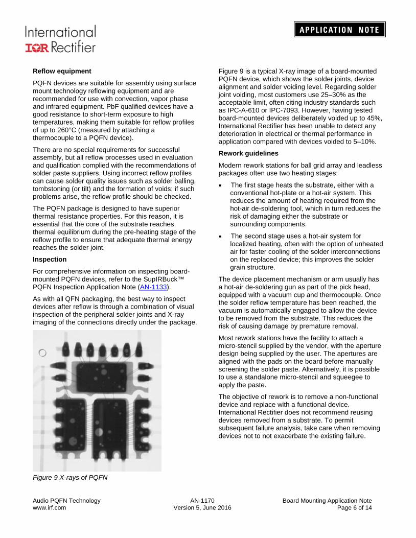
As with all QFN packaging, the best way to inspect devices after reflow is through a combination of visual inspection of the peripheral solder joints and X-ray imaging of the connections directly under the package.
Figure 9 X-rays of PQFN
Figure 9 is a typical X-ray image of a board-mounted PQFN device, which shows the solder joints, device alignment and solder voiding level. Regarding solder joint voiding, most customers use 25–30% as the acceptable limit, often citing industry standards such as IPC-A-610 or IPC-7093. However, having tested board-mounted devices deliberately voided up to 45%, International Rectifier has been unable to detect any deterioration in electrical or thermal performance in application compared with devices voided to 5–10%.
Rework guidelines
Modern rework stations for ball grid array and leadless packages often use two heating stages:
The first stage heats the substrate, either with a conventional hot-plate or a hot-air system. This reduces the amount of heating required from the hot-air de-soldering tool, which in turn reduces the risk of damaging either the substrate or surrounding components.
The second stage uses a hot-air system for localized heating, often with the option of unheated air for faster cooling of the solder interconnections on the replaced device; this improves the solder grain structure.
The device placement mechanism or arm usually has a hot-air de-soldering gun as part of the pick head, equipped with a vacuum cup and thermocouple. Once the solder reflow temperature has been reached, the vacuum is automatically engaged to allow the device to be removed from the substrate. This reduces the risk of causing damage by premature removal.
Most rework stations have the facility to attach a micro-stencil supplied by the vendor, with the aperture design being supplied by the user. The apertures are aligned with the pads on the board before manually screening the solder paste. Alternatively, it is possible to use a standalone micro-stencil and squeegee to apply the paste.
The objective of rework is to remove a non-functional device and replace with a functional device. International Rectifier does not recommend reusing devices removed from a substrate. To permit subsequent failure analysis, take care when removing devices not to not exacerbate the existing failure.
Audio PQFN Technology AN-1170 Board Mounting Application Note www.irf.com Version 5, June 2016 Page 7 of 14
To replace a PQFN device:
Note: If you usually bake to remove residual moisture before rework, insert your normal procedure here.
1. Heat the site to approximately 100°C (150°C for lead-free assembly) using the substrate heating stage.
Note: Pb devices are qualified for a maximum reflow peak temperature of 240°C (260°C for PbF devices). To avoid overheating the device or substrate, adjust the settings on your equipment to achieve a maximum air temperature of 300°C.
2. Lower the placement arm to bring the de-soldering tool into contact with the device. When the device and the solder interconnects reach reflow temperature, lift the placement arm to remove the device from the substrate. Discard the device.
3. Clear residual solder from the site using a blade-type de-soldering tool and de-soldering braid. Clear residual flux using a flux-reducing agent. Take care in cleaning the site: damage to the solder-resist may produce undesirable results.
4. When the site is ready, apply new solder paste with a micro-stencil and squeegee.
5. Position a new device on the vacuum tip of the placement head and lower the placement arm until the device is in contact with the solder paste.
6. Switch off the vacuum on the placement head and retract the placement arm, leaving the device in place.
7. Heat the site to approximately 100°C (150°C for lead-free assembly) using the substrate heating stage.
8. Use the de-soldering tool to heat both device and solder interconnects to reflow temperature, waiting until all the solder has reflowed.
9. Retract the arm, leaving the device in place. Cool as quickly as possible.
Audio PQFN Technology AN-1170 Board Mounting Application Note www.irf.com Version 5, June 2016 Page 8 of 14
Mechanical test results International Rectifier has subjected board-mounted PQFN devices to extensive mechanical tests, conducted in accordance with industry standards and practices. The devices tested were 5x6mm. Given that all Audio PQFN devices are made in the same way, other devices should perform to the same high standard.
This section contains summarized results for bend tests, drop tests and vibration tests.
Standards
JEDEC JESD22B113 Board Level Cyclic Bend Test
JEDEC JESD22B111 Board Level Drop Test
MIL-STD-810F Method 514 Proc. 1. Random Vibration
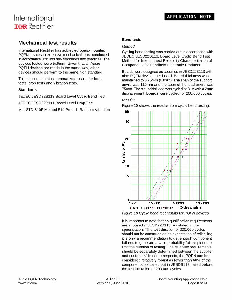
Bend tests
Method Cycling bend testing was carried out in accordance with JEDEC JESD22B113, Board Level Cyclic Bend Test Method for Interconnect Reliability Characterization of Components for Handheld Electronic Products.
Boards were designed as specified in JESD22B113 with nine PQFN devices per board. Board thickness was maintained to 0.75mm (0.030"). The span of the support anvils was 110mm and the span of the load anvils was 75mm. The sinusoidal load was cycled at 3Hz with a 2mm displacement. Boards were cycled for 200,000 cycles.
Results Figure 10 shows the results from cyclic bend testing.
Figure 10 Cyclic bend test results for PQFN devices
It is important to note that no qualification requirements are imposed in JESD22B113. As stated in the specification, “The test duration of 200,000 cycles should not be construed as an expectation of reliability; it is only a recommendation to get enough component failures to generate a valid probability failure plot or to limit the duration of testing. The reliability requirements should be separately determined between the supplier and customer.” In some respects, the PQFN can be considered relatively robust as fewer than 60% of the components, as called out in JESDB113, failed before the test limitation of 200,000 cycles.

Audio PQFN Technology AN-1170 Board Mounting Application Note www.irf.com Version 5, June 2016 Page 9 of 14
Drop tests
Method Drop testing was carried out in accordance with JEDEC JESD22B111, Board Level Drop Test Method of Components for Handheld Electronic Products.
Boards were designed as specified in JESD22B111 with fifteen PQFN devices per board. Board thickness was maintained to 0.75mm (0.030"). The populated assemblies weighed 22g. The calibrated acceleration was 1500G, 0.5 millisecond duration, half-sine pulse which resulted from a 15.5" drop onto a steel block. Figure 11 shows the shock pulse. Each drop was measured with an accelerometer. Each board was dropped 30 times.
Figure 11 Shock pulse for shock test
Results 60 devices were tested and there were no failures.
Vibration tests
Method Vibration testing was carried out as per MIL-STD-810F (Method 514, Proc. 1, Cat. 20 – composite wheeled vehicle). The board design used in vibration testing was equivalent to the design specified in JEDEC JESD22B111, with fifteen PQFN devices per board. A total of four boards were subjected to vibration testing.
The PQFN boards were subjected for four hours to random vibration from 5Hz to 500Hz, experiencing 1.9grms (18.6ms-2
rms) with an acceleration spectral density value of 0.005g2Hz-1 ([0.48ms-2]2Hz-1). Figure 12 shows the bandpass filter frequency chart.
Based on experience with the interconnect failure behavior of similar packages, the devices were only subjected to out-of-plane loading (Z-direction). The test is a pass-fail test and the PQFN devices were tested after the vibration was completed.
Figure 12 Bandpass filter frequency chart
Results 60 devices were tested and there were no failures.
Audio PQFN Technology AN-1170 Board Mounting Application Note www.irf.com Version 5, June 2016 Page 10 of 14
Appendix A Model-specific data This appendix contains the following information about various PQFN devices:
Device outline drawing
Recommended substrate/PCB layout
Suggested designs for stencils of 0.127mm (0.005") thickness
The footprint and stencil designs are recommendations only, and may need to be adjusted to specific requirements. During a study conducted on various package types, International Rectifier found the designs gave repeatable device alignment and proper solder connections.
For more details about individual devices, and to find out their size and outline, refer to the relevant product data sheet.
Interchangeability
Devices of different sizes are not interchangeable.
Acknowledgements
International Rectifier would like to thank DfR Solutions for providing the studies needed to develop the substrate/PCB layouts and stencil designs.
5x6mm outlines
5x6 D
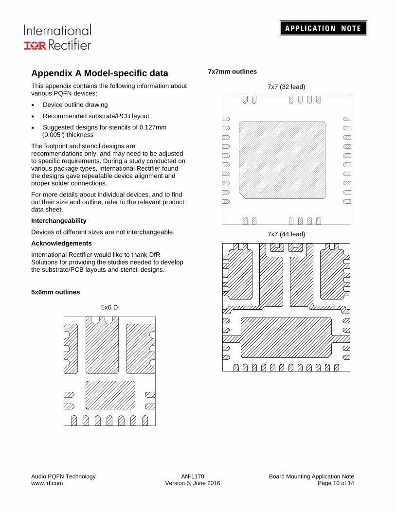
7x7mm outlines
7x7 (32 lead)
7x7 (44 lead)

Audio PQFN Technology AN-1170 Board Mounting Application Note www.irf.com Version 5, June 2016 Page 11 of 14
Appendix A.1 5x6 D devices Device outline
Figure A.1.1 shows the outline for these devices. The relative pad positions are controlled to an accuracy of ±0.050mm. For full dimensions and tolerances of each device, and to find out its size and outline, refer to the relevant product data sheet and package outline drawing.
(dimensions in mm)
Figure A.1.1 5x6 D device outline
Substrate/PCB layout
Evaluations have shown that the best overall performance is achieved using the substrate/PCB layout shown in Figure A.1.2 (a and b).
(dimensions in mm)
Figure A.1.2(a) 5x6 D substrate/PCB layout
(dimensions in mm)
Figure A.1.2(b) 5x6 D substrate/PCB layout
Stencil design
Evaluations have shown that the best overall performance is achieved using the stencil design shown in Figure A.1.3 (a and b).
Note: This design is for a stencil thickness of 0.127mm (0.005"). The reduction should be adjusted for stencils of other thicknesses.
(dimensions in mm)
Figure A.1.3(a) 5x6 D stencil design
(dimensions in mm)
Figure A.1.3(b) 5x6 D stencil design

Audio PQFN Technology AN-1170 Board Mounting Application Note www.irf.com Version 5, June 2016 Page 12 of 14
Appendix A.2 32-lead 7x7 devices Device outline
Figure A.2.1 shows the outline for these devices. The relative pad positions are controlled to an accuracy of ±0.050mm. For full dimensions and tolerances of each device, and to find out its size and outline, refer to the relevant product data sheet and package outline drawing.
37.4
33.6
1.763.2
(dimensions in mm)
Figure A.2.1 32-lead 7x7 device outline
Substrate/PCB layout
Evaluations have shown that the best overall performance is achieved using the substrate/PCB layout shown in Figure A.2.2 (a and b).
0.2400.700
4.675
4.200
0.35
0.35
0.700
0.240
(dimensions in mm)
Figure A.2.2(a) 32-lead 7x7 substrate/PCB layout
0.500 2.0001.690
1.189
0.500
1.190
1.988 2.013
2.250
2.250
1.190
1.690 1.190
1.190
1.189
(dimensions in mm)
Figure A.2.2(b) 32-lead 7x7 substrate/PCB layout
Stencil design
Evaluations have shown that the best overall performance is achieved using the stencil design shown in Figure A.2.3 (a and b).
Note: This design is for a stencil thickness of 0.127mm (0.005"). The reduction should be adjusted for stencils of other thicknesses.
0.2200.650
1.200
1.100 0.2200.650
(dimensions in mm)
Figure A.2.3(a) 7x7 stencil design 0.500
2.0001.558 1.558
1.40
01.
400
1.1741.675
1.175
1.174
0.500 0.500
1.175
1.675
1.175
0.429 0.454
0.850
0.850
1.175
(dimensions in mm)
Figure A.2.3(b) 7x7 stencil design
Audio PQFN Technology AN-1170 Board Mounting Application Note www.irf.com Version 5, June 2016 Page 13 of 14
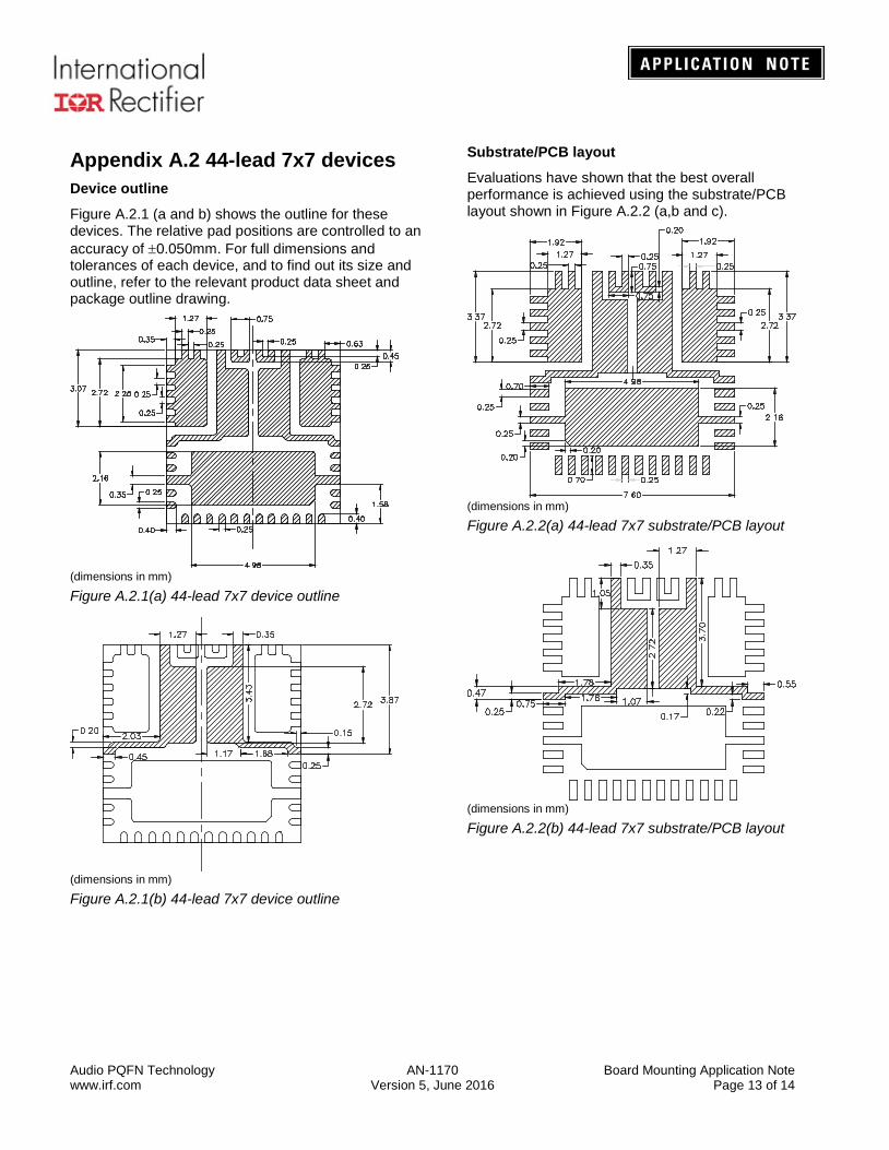
Appendix A.2 44-lead 7x7 devices Device outline
Figure A.2.1 (a and b) shows the outline for these devices. The relative pad positions are controlled to an accuracy of ±0.050mm. For full dimensions and tolerances of each device, and to find out its size and outline, refer to the relevant product data sheet and package outline drawing.
(dimensions in mm)
Figure A.2.1(a) 44-lead 7x7 device outline
(dimensions in mm)
Figure A.2.1(b) 44-lead 7x7 device outline
Substrate/PCB layout
Evaluations have shown that the best overall performance is achieved using the substrate/PCB layout shown in Figure A.2.2 (a,b and c).
(dimensions in mm)
Figure A.2.2(a) 44-lead 7x7 substrate/PCB layout
(dimensions in mm)
Figure A.2.2(b) 44-lead 7x7 substrate/PCB layout

Audio PQFN Technology AN-1170 Board Mounting Application Note www.irf.com Version 5, June 2016 Page 14 of 14
(dimensions in mm)
Figure A.2.2(c) 7x7 substrate/PCB layout
Stencil design
Evaluations have shown that the best overall performance is achieved using the stencil design shown in Figure A.2.3 (a, b and c).
Note: This design is for a stencil thickness of 0.127mm (0.005"). The reduction should be adjusted for stencils of other thicknesses.
(dimensions in mm)
Figure A.2.3(a) 7x7 stencil design
(dimensions in mm)
Figure A.2.3(b) 7x7 stencil design
(dimensions in mm)
Figure A.2.3(c) 7x7 stencil design