apodis ii product description - ip light ports support otu2, otu2e/1e, otu2f/1f, otu2i/1i and otu1...
TRANSCRIPT

Apodis II
Product Description
Version 1.01 April 2013 Copyright © 2013 by IP Light Ltd.

Copyright © 2013 by IP Light Ltd.
All rights reserved.
IP Light reserves the right to make changes to its products, its data sheets, or related documentation, without
notice and warrants its products solely pursuant to its terms and conditions of sale, only to substantially comply
with the latest available data sheet. Please consult IP Light’s Term and Conditions of Sale for its warranties and
other terms, conditions, and limitations. IP Light may discontinue any semiconductor product or service without
notice, and advises its customers to obtain the latest version of relevant information to verify, before placing
orders, that the information is current. IP Light does not assume any liability arising out of the application or use
of any product or circuit described herein, neither does it convey any license under its patent rights nor the rights
of others. IP Light reserves the right to ship devices of higher grade in place of those of lower grade.
IP LIGHT SEMICONDUCTOR PRODUCTS ARE NOT DESIGNED, INTENDED, AUTHORIZED, OR
WARRANTED TO BE SUITABLE FOR USE IN LIFE-SUPPORT APPLICATIONS, DEVICES OR
SYSTEMS, OR OTHER CRITICAL APPLICATIONS.
IP Light Ltd.
4 Hashiloach Street
PO Box 7209
Petach Tikva 49250
Israel
April 23, 2013

Creating an Intelligent Optical Layer Apodis II Product Description
iii Version History
IP Light Proprietary and Confidential
Version History
The following table chronicles the changes made to the Apodis II Product Description.
Table 1: Version History
Version Date Description
1.00 February 2013 Initial version release.
1.01 April 2013 Updates made to conform to the Apodis II Datasheet v1.00, including the following:
Getting Started section
Apodis II High Level System Description chapter
IPL4002M, IPL4102M and IPL4202M Client Signal Processor Detailed Block figure
Loopbacks section
Timestamp Timer section
Multiservice OTU4 Multiplexers section
Protected Multiservice Interface Card section
Next Generation Fronthaul section

Creating an Intelligent Optical Layer Apodis II Product Description
iv Contents
IP Light Proprietary and Confidential
Contents
VERSION HISTORY ........................................................................................................................ III
CONTENTS .................................................................................................................................. IV
FIGURES...................................................................................................................................... VI
TABLES ..................................................................................................................................... VIII
APODIS II FAMILY OTN PROCESSORS ............................................................................................ X Key Features ......................................................................................................................................................................... x
GETTING STARTED .......................................................................................................................XI
ABOUT THIS DOCUMENT ............................................................................................................. XII Related Documents ............................................................................................................................................................. xii
Document Conventions ........................................................................................................................................ xiii Terminology Conventions ................................................................................................................................................... xiii Design Conventions ............................................................................................................................................................ xiii Notes and Warnings ........................................................................................................................................................... xiii
1 APODIS II HIGH LEVEL SYSTEM DESCRIPTION ......................................................................... 1 1.1 Data Flow ....................................................................................................................................................... 3
1.2 Mapping Options............................................................................................................................................ 6
1.3 Cross Connections ........................................................................................................................................ 10
2 APODIS II DETAILED DESCRIPTION ....................................................................................... 12 2.1 Client Signal Processor ................................................................................................................................. 12
2.1.1 Client Signal Processor Block Details ................................................................................................................... 13 2.1.2 Client Signal Types ............................................................................................................................................... 15
2.2 Network Signal Processor ............................................................................................................................ 35 2.2.1 Network Signal Processor Block Details ............................................................................................................... 35 2.2.2 Network Signal Types .......................................................................................................................................... 38
2.3 IPLightSERDES™ ............................................................................................................................................ 43 2.3.1 IPLightSERDES™ Block Details .............................................................................................................................. 43 2.3.2 IPLightSERDES™ Maintenance ............................................................................................................................. 44 2.3.3 IPLightSERDES™ Standards Compliance............................................................................................................... 45 2.3.4 IPLightSERDES™ Physical Interfaces ..................................................................................................................... 46
2.4 Transparent Agnostic Fabric ........................................................................................................................ 48
2.5 Overhead Access .......................................................................................................................................... 48 2.5.1 External Overhead Interface ................................................................................................................................ 48 2.5.2 Overhead Operator .............................................................................................................................................. 49
2.6 Host Processor Interface .............................................................................................................................. 50
3 APODIS II PROCESSES .......................................................................................................... 51 3.1 OTN Performance Monitoring ..................................................................................................................... 51
3.1.1 Performance Monitoring Counters ...................................................................................................................... 51 3.1.2 Tandem Connection Monitoring .......................................................................................................................... 52 3.1.3 Delay Measurement ............................................................................................................................................ 52
3.2 OTN Alarms and Indications ......................................................................................................................... 53 3.2.1 Consequent Actions ............................................................................................................................................. 54 3.2.2 Defect Correlation ............................................................................................................................................... 54
3.3 Interrupts ..................................................................................................................................................... 54

Creating an Intelligent Optical Layer Apodis II Product Description
v Contents
IP Light Proprietary and Confidential
4 JTAG INTERFACE ................................................................................................................. 55
5 TIMESTAMP TIMER ............................................................................................................. 56
6 CLOCKS ............................................................................................................................... 57
7 POWER ............................................................................................................................... 59
8 RESET ................................................................................................................................. 60
9 APPLICATION EXAMPLES ..................................................................................................... 61 9.1 Muxponder................................................................................................................................................... 62
9.2 Multiservice OTU4 Multiplexers .................................................................................................................. 63
9.3 Protected Multiservice Interface Card ......................................................................................................... 64
9.4 OTN Line Cards for Centralized Switching Fabrics Systems ......................................................................... 65
9.5 OTN Network PT20/PT21 Gateway .............................................................................................................. 66
9.6 Next Generation Fronthaul .......................................................................................................................... 67
10 PACKAGE INFORMATION .................................................................................................... 68
11 ORDERING INFORMATION................................................................................................... 69
GLOSSARY .................................................................................................................................. 70
READER COMMENTS ................................................................................................................... 73

Creating an Intelligent Optical Layer Apodis II Product Description
vi Figures
IP Light Proprietary and Confidential
Figures
Figure 1: IPL4002M/IPL4302F Block Diagram .......................................................................................... 1
Figure 2: IPL4102M Block Diagram .......................................................................................................... 1
Figure 3: IPL4202M Block Diagram .......................................................................................................... 2
Figure 4: IPL4402F Block Diagram ............................................................................................................ 2
Figure 5: GbE to OTU2 Example ............................................................................................................... 3
Figure 6: OTU2 Add/Drop Example .......................................................................................................... 4
Figure 7: IPL4102M Client Side Multiplexing Example ............................................................................ 5
Figure 8: IPL4002M, IPL4102M and IPL4202M Network Side Multiplexing and Mapping ...................... 7
Figure 9: IPL4302F and IPL4402F Network Side Mapping ....................................................................... 8
Figure 10: IPL4002M, IPLM4102M and IPL4202M Client Side Multiplexing and Mapping ..................... 9
Figure 11: IPL4302F and IPL4402F Client Side Multiplexing and Mapping ............................................ 10
Figure 12: IPL4002M, IPL4102M and IPL4202M Client Signal Processor Detailed Block ...................... 13
Figure 13: IPL4302F and IPL4402F Client Signal Processor Detailed Block ............................................ 14
Figure 14: 10GE Processing .................................................................................................................... 16
Figure 15: FC-1200 Processing ............................................................................................................... 17
Figure 16: OTU2 Processing ................................................................................................................... 18
Figure 17: OTU1 Processing ................................................................................................................... 19
Figure 18: OTU0 Processing ................................................................................................................... 20
Figure 19: GbE Processing ...................................................................................................................... 20
Figure 20: OAM Functions ..................................................................................................................... 21
Figure 21: FE Processing......................................................................................................................... 22
Figure 22: FC-100 Processing ................................................................................................................. 22
Figure 23: ESCON Processing ................................................................................................................. 23
Figure 24: FC-200 Processing ................................................................................................................. 23
Figure 25: FC-400 and FC-800 Processing .............................................................................................. 24
Figure 26: OC-192/STM-64/CBR10G Processing .................................................................................... 24
Figure 27: OC-48/STM-16 Processing .................................................................................................... 25
Figure 28: OC-3/STM-1 and OC-12/STM-4 Processing .......................................................................... 26
Figure 29: CPRI Options 1 and 2 Processing .......................................................................................... 28
Figure 30: CPRI Option 3 Processing ...................................................................................................... 28
Figure 31: CPRI Options 4 and 5 Processing .......................................................................................... 29
Figure 32: CPRI Option 7 Processing ...................................................................................................... 29
Figure 33: DVB-ASI Processing ............................................................................................................... 29
Figure 34: 270M SDI Processing ............................................................................................................. 30
Figure 35: 1.5G SDI Processing ............................................................................................................... 30
Figure 36: 3G SDI Processing .................................................................................................................. 31
Figure 37: IB SDR and DDR Processing ................................................................................................... 31

Creating an Intelligent Optical Layer Apodis II Product Description
vii Figures
IP Light Proprietary and Confidential
Figure 38: IB QDR Processing ................................................................................................................. 32
Figure 39: CBR0 Processing .................................................................................................................... 32
Figure 40: CBR1 Processing .................................................................................................................... 33
Figure 41: CBR2 Processing .................................................................................................................... 33
Figure 42: CBRflex Processing ................................................................................................................ 34
Figure 43: IPL4002M, IPL4102M and IPL4202M Network Signal Processor for OTU2 Lines Detailed Block ....................................................................................................................................................... 35
Figure 44: IPL4102M Network Signal Processor for ODU2 Lines Detailed Block ................................... 36
Figure 45: IPL4202M Network Signal Processor for OTU1 Lines Detailed Block ................................... 36
Figure 46: IPL4102M Network Signal Processor for OTU1Aux Lines Detailed Block ............................. 37
Figure 47: IPL4302F and IPL4402F Network Signal Processor Detailed Block ....................................... 37
Figure 48: FEC Performance ................................................................................................................... 40
Figure 49: IPLightSERDES™ Block Diagram ............................................................................................ 43
Figure 50: End-to-End Loopback Path .................................................................................................... 44
Figure 51: TAF Functional Block Diagram .............................................................................................. 48
Figure 52: External Overhead Interface ................................................................................................. 49
Figure 53: Overhead Byte Transformer ................................................................................................. 49
Figure 54: TCM Handling ........................................................................................................................ 52
Figure 55: Delay Measurement .............................................................................................................. 53
Figure 56: Master IRQ Generation ......................................................................................................... 54
Figure 57: Timestamp Timer .................................................................................................................. 56
Figure 58: Clock Selection ...................................................................................................................... 57
Figure 59: Clock Outputs ........................................................................................................................ 57
Figure 60: OTN Network Topology ........................................................................................................ 61
Figure 61: Muxponder—Any Signal to OTU2 ......................................................................................... 62
Figure 62: Multiservice OTU4 Multiplexer ............................................................................................. 63
Figure 63: Protected Multiservice Interface Card .................................................................................. 64
Figure 64: Network Line Card ................................................................................................................ 65
Figure 65: OTN Network Gateway ......................................................................................................... 66
Figure 66: Mobile Fronthaul Optimization ............................................................................................ 67

Creating an Intelligent Optical Layer Apodis II Product Description
viii Tables
IP Light Proprietary and Confidential
Tables
Table 1: Version History .......................................................................................................................... iii
Table 2: Apodis II Family of OTN Processors ........................................................................................... xi
Table 3: Signal Mapping Options ............................................................................................................. 6
Table 4: Client to Client Cross Connections ........................................................................................... 10
Table 5: IPL4102M Client to Client Cross Connections Including OTN Multiplexing ............................. 11
Table 6: 10GE Client Interface Signal Rate ............................................................................................. 16
Table 7: FC-1200 Client Interface Signal Rates ...................................................................................... 17
Table 8: OTU2/ODU2 Client Interface Signal Rates ............................................................................... 18
Table 9: OTU1 Client Interface Signal Rate ............................................................................................ 19
Table 10: OTU0 Client Interface Signal Rate .......................................................................................... 20
Table 11: GbE Client Interface Signal Rate ............................................................................................. 21
Table 12: FE Client Interface Signal Rate ............................................................................................... 22
Table 13: FC-100 Client Interface Signal Rate ........................................................................................ 22
Table 14: ESCON Client Interface Signal Rate ........................................................................................ 23
Table 15: FC-200 Client Interface Signal Rate ........................................................................................ 23
Table 16: FC-400 and FC-800 Client Interface Signal Rates ................................................................... 24
Table 17: OC-192/STM-64/CBR10G Client Interface Signal Rates ......................................................... 25
Table 18: OC-48/STM-16/CBR2G5 Client Interface Signal Rate ............................................................. 26
Table 19: OC-3/STM-1 and OC-12/STM-4 Client Interface Signal Rates ................................................ 27
Table 20: CPRI Options 1 and 2 Client Interface Signal Rates ................................................................ 28
Table 21: CPRI Option 3 Client Interface Signal Rate ............................................................................. 28
Table 22: CPRI Options 4 and 5 Client Interface Signal Rates ................................................................ 29
Table 23: CPRI Option 7 Client Interface Signal Rate ............................................................................. 29
Table 24: DVB-ASI Client Interface Signal Rate ...................................................................................... 30
Table 25: 270M SDI Client Interface Signal Rate ................................................................................... 30
Table 26: 1.5G SDI Client Interface Signal Rates .................................................................................... 31
Table 27: 3G SDI Client Interface Signal Rates ....................................................................................... 31
Table 28: IB SDR and DDR Client Interface Signal Rates ........................................................................ 31
Table 29: IB QDR Client Interface Signal Rates ...................................................................................... 32
Table 30: CBR0 Client InterfaceSignal Rates .......................................................................................... 32
Table 31: CBR1 Client Interface Signal Rates ......................................................................................... 33
Table 32: CBR2 Client Interface Signal Rates ......................................................................................... 33
Table 33: CBRflex Client Interface Signal Rates ..................................................................................... 34
Table 34: OTU2 Network Interface Signal Rates .................................................................................... 39
Table 35: ODU2 Network Interface Signal Rates ................................................................................... 41
Table 36: OTU1 Network Interface Signal Rate ..................................................................................... 42
Table 37: OTU1Aux Network Interface Signal Rate ............................................................................... 43

Creating an Intelligent Optical Layer Apodis II Product Description
ix Tables
IP Light Proprietary and Confidential
Table 38: XAUI Clock Rates .................................................................................................................... 47
Table 39: SFI4.2 Clock Rates ................................................................................................................... 47
Table 40: Subset of Alarms and Indications ........................................................................................... 53
Table 41: Typical Power Dissipation ...................................................................................................... 59
Table 42: Part Number ........................................................................................................................... 69
Table 43: Glossary of Terms ................................................................................................................... 70

Creating an Intelligent Optical Layer Apodis II Product Description
x Apodis II Family OTN Processors
IP Light Proprietary and Confidential
Apodis II Family OTN Processors
The Apodis II family of ITU-T compliant Optical Transport Network (OTN) processors includes the IPL4002M, IPL4102M, IPL4202M, IPL4302F and IPL4402F members. The Apodis II processors offer termination, processing, framing, multiplexing, demultiplexing and switching of OTN signals, in addition to client side mapping of SONET/SDH, Ethernet, Storage Area Network (SAN), Video, InfiniBand and Common Public Radio Interface (CPRI) signals to OTN signals. The client side supports up to 16 ports of any-service any-port, and the network side supports up to four 10 Gbps ports of full OTN capability, resulting in full duplex bandwidth of up to 40 Gbps. The Apodis II processors incorporate a fully available, non-blocking OTN switching fabric, allowing switching between client/network, client/client, and network/network ports. The flexibility and high bandwidth that the Apodis II processors provide makes them ideal for 4G optical wireless backhaul/fronthaul, next-generation access and optical networking edge, metro, metro-core and long haul applications.
Key Features
Network ports support OTU2, OTU2e/1e, OTU2f/1f, OTU2i/1i and OTU1 signals
Configurable network ports support serial (XFI or SFI), SFI 4.2 and XBI2 (two or four lane) interfaces
Client ports support the following signals:
FE/GbE/10GE FC-100/FC-200/FC-400/FC-800/
FC-1200 SONET OC-3/OC-12/OC-48/OC-192 SDH STM-1/STM-4/STM-16/STM-64 CPRI Options 1-5, 7 DVB-ASI, 270M SDI, 1.5G SDI, 3G SDI IB SDR/DDR/QDR Arbitrary bit rate OTN OTU0/OTU1/OTU2/OTU1e/
OTU2e/OTU1f/OTU2f/OTU1i/OTU2i
Configurable client ports support serial (XFI or SFI), XAUI, SFI 4.2 and XBI2 (two or four lane) interfaces
Maps client signals to OTN ODU0/1/2/flex signals
Non-blocking, fully transparent switch fabric for OTN signals with the following capabilities:
ODU0/1/2/flex switching granularity Multicasting
Provides six levels of TCM (tandem connection monitoring) overhead processing for all ODU0/1/2/flex signals
Includes standard G.709 GFEC for all OTU0/1/2 signals, plus Enhanced (ITU-T G.975.1 I.4) and Ultra (ITU-T G.975.1 I.7) FEC for network side OTU2 signals
Roundtrip delay measurements on ODU and TCM paths
Supports OTN Performance Monitoring counters, alarms and indications
Full internal processing of all OTN overhead bits
Terminal and line loopback capabilities support network level fault isolation, as well as integrated test signal generators and detectors
Full access to all OTN overhead fields, including GCC0/1/2
Multiple Performance Monitoring (PM) options, PM counters, alarms, indications and optional regeneration of SONET/SDH section and line overheads
Access to SONET/SDH section and line overhead fields
RMON
GbE link layer OAM
Carrier Ethernet OA&M support
IEEE 1588v2 support (GbE)
Multi-gigabit IPLightSERDES™ supports any-service, any-port configurations from 125 MB to 11.4 G
Integrated jitter attenuators meet or exceed telecom and data communication standards with no need for external components
Integrated synthesizers generate all required internal timing from a single external reference clock
Intel/Freescale host interface bus
Power management
Package: 31 x 31 mm, 896 pin HFC-BGA
Supply voltages: 1V and 2.5V
RoHS compliant

Creating an Intelligent Optical Layer Apodis II Product Description
xi Getting Started
IP Light Proprietary and Confidential
Getting Started
The following table shows the Apodis II processors family, which leverages the same architecture to address various applications.
Table 2: Apodis II Family of OTN Processors
Product Name
Client Ports
Network Ports Capacity
Client Signals Network Signals
STM-1/4/16 OC-3/12/48
OTU0/1 FE/GbE ESCON
FC-100/200/400/800 270M/1.5G/3G SDI
DVB-ASI IB SDR/DDR
CPRI Options 1-5 Arbitrary Bit-rate
STM-64 OC-192 OTU2 10GE
FC-1200 IB QDR
CPRI Option 7 Arbitrary Bit-rate OTU1 OTU2
IPL4002M 16 4 40G
IPL4102M 16 2 20G
IPL4202M 8 4 or 1 10G
IPL4302F 4 4 40G
IPL4402F 2 2 20G

Creating an Intelligent Optical Layer Apodis II Product Description
xii About This Document
IP Light Proprietary and Confidential
About This Document
The Apodis II Product Description provides a general overview of the Apodis II processors family, the primary component of IP Light's comprehensive OTN solution. This Product Description is organized as follows:
Apodis II High Level System Description in Section 1 provides a high level overview of the
Apodis II
Apodis II Detailed Description in Section 2 provides detailed descriptions of the Apodis II high
level blocks
Apodis II Processes in Section 3 provides detailed descriptions of the mechanisms supporting the Apodis II high level blocks
JTAG Interface in Section 4 provides information about the JTAG interface supported by the Apodis II
Timestamp Timer in Section 5 describes the timestamp timer to record the exact arrival and
transmit time of GbE selected frames.
Clocks in Section 6 describes the transmit PLLs used by the Apodis II CSP and NSP
Power in Section 7 describes how the Apodis II provides flexible operational modes
Reset in Section 8 describes the Apodis II reset mechanisms
Application Examples in Section 9 provides examples of different applications that highlight some of the many ways in which the Apodis II can be used
Package Information in Section 10 provides Apodis II package details
Ordering Information in Section 11 provides Apodis II ordering details
Related Documents
This Apodis II Product Description is intended to be used together with the documents listed below; they contain information and instructions that supplement this document. This Product Description instructs you when to refer to these documents.
Apodis II Datasheet—provides functional information on using the Apodis II
Apodis II User Manual—provides in depth information pertaining to the configuration and operation of the Apodis II

Creating an Intelligent Optical Layer Apodis II Product Description
xiii About This Document
IP Light Proprietary and Confidential
Document Conventions
This document uses the following term and design conventions.
Terminology Conventions
Except where otherwise noted, these terminology conventions are used throughout the document:
Text refers to all Apodis II family members, unless otherwise specified
The signal type "OTU2" includes OTU2/1e/2e/1f/2f/1i/2i
The signal type "ODU2" includes ODU2/2e/1e/2f/1f/1i/2i
The signal type "OPU2" includes OPU2/2e/1e/2f/1f/1i/2i
"10 G" or "10 Gbps" is intended only as a descriptor, while the actual signal nominal rate may vary between 9.953 Gbps for OC-192 and 11.318 Gbps for OTU2f
"2.5 G" and "5 G" are intended as descriptors, while the actual signal rate may vary
Constant Bit Rate (CBR) signals refer to any arbitrary constant bit rate client signals that are mapped, according to their bit rate, to their relevant ODU container. The CBR signals are defined as follows:
"CBR0" arbitrary bit rate signals mapped to ODU0 "CBR1" arbitrary bit rate signals mapped to ODU1 "CBR2" arbitrary bit rate signals mapped to ODU2 "CBRflex" arbitrary bit rate signals mapped to ODUflex
Hexadecimal numbers are prefixed with "0x"
Binary numbers are suffixed with the letter "b"
The names "network" and "line" are interchangeable, both representing the side of the chip opposite of the client side
Design Conventions
This document uses the following conventions:
Commands and keywords are in boldface font
Arguments for which you supply values are in italic font
Terminal sessions and information the system displays are in screen font
Information you must enter is in boldface screen font
Elements in square brackets ([ ]) are optional
Notes and Warnings
Notes use the following conventions:
NOTE—Means reader take note. Notes contain helpful suggestions or references to material not
covered in the publication.
IMPORTANT—An important note provides information that is essential to the completion of a task. Although information may be disregarded in a note and still complete a task, but an important note should not be disregarded.
The information in a caution or a warning is provided for your protection. Please read each caution and warning carefully.
CAUTION—Indicates possibility of service interruption if precautions are not taken.
WARNING—Indicates possibility of damage to the device if precautions are not taken.

Creating an Intelligent Optical Layer Apodis II Product Description
1 Apodis II High Level System Description
IP Light Proprietary and Confidential
1 Apodis II High Level System Description The following figures show the high level block diagrams for each of the Apodis II family processors.
TAFClient Signal
Processor
CSP 0
Network Signal
Processor
NSP 0
Client Signal
Processor
CSP 1
Network Signal
Processor
NSP 1
Client Signal
Processor
CSP 2
Network Signal
Processor
NSP 2
Client Signal
Processor
CSP 3
Network Signal
Processor
NSP 3
Client 13
Client 14
Client 15
Lane 0
Lane 1
Lane 2
Lane 3
Client 1
Client 2
Client 3
Client 4
Client 5
Client 6
Client 7
Client 8
Client 9
Client 10
Client 11
Client 12
Lane 0
Lane 1
Lane 2
Lane 3
Lane 0
Lane 1
Lane 2
Lane 3
Lane 0
Lane 1
Lane 2
Lane 3
Co
ntr
ol
Ad
dr
Bu
s m
od
e
Host Processor Interface
HP
I clo
ck
EO
I clo
ck
Tim
eslo
t
Co
ntr
ol
External Overhead
Interface
Re
f clo
ck
Hig
h r
ate
clo
cks
Re
se
t
Lo
w r
ate
clo
cks
Clocks & Reset
Da
ta
Da
ta
SERDES
SERDES
SERDES
SERDES
SERDES
SERDES
SERDES
SERDES
SERDES
SERDES
SERDES
SERDES
SERDES
SERDES
SERDES
SERDES
SERDES
SERDES
SERDES
SERDES
SERDES
SERDES
SERDES
SERDES
SERDES
SERDES
SERDES
SERDES
SERDES
SERDES
SERDES
SERDES
Lane 0
Lane 1
Lane 2
Lane 3
Lane 0
Lane 1
Lane 2
Lane 3
Lane 0
Lane 1
Lane 2
Lane 3
Lane 0
Lane 1
Lane 2
Lane 3
Client 0
OTU2
OTU2
OTU2
OTU2
Figure 1: IPL4002M/IPL4302F Block Diagram
TAFClient Signal
Processor
CSP 0
Network Signal
Processor
NSP 0
Client Signal
Processor
CSP 1
Network Signal
Processor
NSP 1
Client Signal
Processor
CSP 2
Network Signal
Processor
NSP 2
Client Signal
Processor
CSP 3
Network Signal
Processor
NSP 3
OTU2
Client 13
Client 14
Client 15
Lane 0
Lane 1
Lane 2
Lane 3
Client 1
Client 2
Client 3
Client 4
Client 5
Client 6
Client 7
Client 8
Client 9
Client 10
Client 11
Client 12
Lane 0
Lane 1
Lane 2
Lane 3
Lane 0
Lane 1
Lane 2
Lane 3
Lane 0
Lane 1
Lane 2
Lane 3
Co
ntr
ol
Ad
dr
Bu
s m
od
e
Host Processor Interface
HP
I clo
ck
EO
I clo
ck
Tim
eslo
t
Co
ntr
ol
External Overhead
Interface
Re
f clo
ck
Hig
h r
ate
clo
cks
Re
se
t
Lo
w r
ate
clo
cks
Clocks & Reset
Da
ta
Da
ta
SERDES
SERDES
SERDES
SERDES
SERDES
SERDES
SERDES
SERDES
SERDES
SERDES
SERDES
SERDES
SERDES
SERDES
SERDES
SERDES
SERDES
SERDES
SERDES
SERDES
SERDES
SERDES
SERDES
SERDES
SERDES
SERDES
SERDES
SERDES
SERDES
SERDES
SERDES
SERDES
Lane 0
Lane 1
Lane 2
Lane 3
Lane 0
Lane 1
Lane 2
Lane 3
Client 0
OTU2
ODU2 or
4xOTU1Aux
Lane 0
Lane 1
Lane 2
Lane 3
ODU2 or
4xOTU1Aux
Lane 0
Lane 1
Lane 2
Lane 3
Figure 2: IPL4102M Block Diagram

Creating an Intelligent Optical Layer Apodis II Product Description
2 Apodis II High Level System Description
IP Light Proprietary and Confidential
TAFClient Signal
Processor
CSP 0
Network Signal
Processor
NSP 0
Client Signal
Processor
CSP 1
Network Signal
Processor
NSP 1
Network Signal
Processor
NSP 2
Network Signal
Processor
NSP 3
Client 1
Client 2
Client 3
Client 4
Client 5
Client 6
Client 7
Lane 0
Lane 1
Lane 2
Lane 3
Lane 0
Lane 1
Lane 2
Lane 3
Co
ntr
ol
Ad
dr
Bu
s m
od
e
Host Processor Interface
HP
I clo
ck
EO
I clo
ck
Tim
eslo
t
Co
ntr
ol
External Overhead
Interface
Re
f clo
ck
Hig
h r
ate
clo
cks
Re
se
t
Lo
w r
ate
clo
cks
Clocks & Reset
Da
ta
Da
ta
SERDES
SERDES
SERDES
SERDES
SERDES
SERDES
SERDES
SERDES
SERDES
SERDESLane 0
Lane 0
Client 0
OTU1
OTU1
SERDESLane 0
OTU1
SERDES
SERDES
SERDES
SERDES
OTU2 or Single OTU1
(Lane 0 only)
Lane 0
Lane 1
Lane 2
Lane 3
Figure 3: IPL4202M Block Diagram
TAFClient Signal
Processor
CSP 0
Network Signal
Processor
NSP 2
Client Signal
Processor
CSP 1
Network Signal
Processor
NSP 3
Client 1
Client 2
Client 3
Client 4
Client 5
Client 6
Client 7
Lane 0
Lane 1
Lane 2
Lane 3
Lane 0
Lane 1
Lane 2
Lane 3
Co
ntr
ol
Ad
dr
Bu
s m
od
e
Host Processor Interface
HP
I clo
ck
EO
I clo
ck
Tim
eslo
t
Co
ntr
ol
External Overhead
Interface
Re
f clo
ck
Hig
h r
ate
clo
cks
Re
se
t
Lo
w r
ate
clo
cks
Clocks & Reset
Da
ta
Da
ta
SERDES
SERDES
SERDES
SERDES
SERDES
SERDES
SERDES
SERDES
SERDES
SERDES
SERDES
SERDES
SERDES
SERDES
SERDES
SERDES
Lane 0
Lane 1
Lane 2
Lane 3
Lane 0
Lane 1
Lane 2
Lane 3
Client 0
OTU2
OTU2
Figure 4: IPL4402F Block Diagram
The high level blocks are described in the following sections, including:
Data Flow in Section 1.0
Mapping Options in Section 1.2
Cross Connections in Section 1.3

Creating an Intelligent Optical Layer Apodis II Product Description
3 Apodis II High Level System Description Data Flow
IP Light Proprietary and Confidential
1.1 Data Flow
The Apodis II contains Client Signal Processor (CSP) blocks, Network Signal Processor (NSP) blocks, IPLightSERDES™ blocks, and the Transparent Agnostic Fabric (TAF) switching block at its core. The Apodis II interfaces are compliant with the relevant standards. The NSP supports OTN signals, while the CSP supports a variety of signal types, which can be mapped into OTN bearer signals, in addition to supporting OTN signals. The Apodis II also contains a generic host interface for configuration and monitoring, and an External Overhead Interface (EOI) that enables access into the OTN and SONET/SDH overheads.
The basic data flows of the Apodis II are as follows:
Client port to network port data flow:
1. Traffic enters the device through one of the client ports. The data is then passed through and processed, as follows:
Monitored for alarms and degradations Mapped into an appropriate OTN payload
2. Data passes through the switch fabric (TAF) and if required, it is also multiplexed at this point in the flow.
3. Data is forwarded to the network ports for transmission to the OTN network.
Network port to client port data flow:
1. Traffic enters from one of the network ports and is monitored for alarms and degradations.
If required, the data is demapped or demultiplexed at this point in the flow.
2. Data passes through the TAF. 3. Data is converted into the desired output signal type. 4. Data is sent out from one of the client ports.
The TAF switching capability also enables connections between network to network and client to client ports.
NOTE—Some limitations apply to client to client cross-connections, see Apodis II User Manual for
specific information.
The following figure shows an example of Gigabit Ethernet (GbE) to OTU2 client to network capabilities for IPL4002M, IPL4102M and IPL4202M processors.
TAF
OP
U2
OD
U2
OT
U2
GbE
ClientOTU2
GbE
GbE
GbE
GbE
GbE
GbE
GbE
GbE
Figure 5: GbE to OTU2 Example

Creating an Intelligent Optical Layer Apodis II Product Description
4 Apodis II High Level System Description Data Flow
IP Light Proprietary and Confidential
GbE to OTU2 data flow:
1. The device receives eight GbE signals from the client side. 2. These signals are rate adapted using GFP-T and then GMP mapped into eight ODU0 signals. 3. ODU0 signals are GMP mapped into ODTU02, which are then multiplexed into the tributary slots
of an OPU2. 4. OTU2 is generated from the OPU2 and transmitted from the network side.
OTU2 to GbE data flow:
1. OTU2 signal is received from the network side and OPU2 is extracted. 2. ODU0 signals are GMP demapped from ODTU02 signals, which were demultiplexed from the
tributary slots of the OPU2. 3. The GFP-T signals are GMP demapped from the ODU0 signals. 4. GFP-T signals are terminated and the GbE signals are extracted. 5. The GbE signals are transmitted to the client side.
The following figure shows an example of an add/drop application involving four network side OTU2s and dropping a combination of different client signals for IPL4002M.
TAF
West East
ODU0
ODUflex
ODUflex
ODU0
OP
U2
OD
U2
OT
U2
OTU2
OP
U2
OD
U2
OT
U2
OTU2
ODU0
ODU1
ODUflex
ODU1
ODU0
ODUflex
ODU1
ODU1
OP
U2
OD
U2
OT
U2
OTU2
ODU0
ODU1
ODUflex
ODU1
OP
U2
OD
U2
OT
U2
OTU2
OP
U1
OD
U1
1.5
G S
DI
ODUfle
xO
PU
flex
CP
RI O
ptio
n 4
OD
U0
OP
U0
Gb
E
OD
U0
OP
U0
ST
M-1
/OC
-3
ODUfle
xO
PU
flex
IB S
DR
OP
U1
OD
U1
FC
-20
0
OP
U1
OD
U1
ST
M-1
6/O
C-4
8
OD
U0
OP
U0
FC
-10
0
ODUfle
xO
PU
flex
3G
SD
I
OP
U1
OD
U1
CP
RI O
ptio
n 3
Figure 6: OTU2 Add/Drop Example
The West side OTU2 signals enter the device and are demultiplexed into ODU1, ODUflex and ODU0 signals. One ODU1 signal, one ODUflex signal and one ODU0 signal are passed through the TAF to the EAST side OTU2 output. Two ODU0 signals and one ODUflex signal from the West side OTU2 and two ODU1 signals and one ODU0 signal from the East side OTU2 are used for add/drop.

Creating an Intelligent Optical Layer Apodis II Product Description
5 Apodis II High Level System Description Data Flow
IP Light Proprietary and Confidential
The following figure shows an example of client side OTN multiplexing for the IPL4102M.
ODU2 Tandem
CSP3
OTU1 Tandem
OTU1 Tandem
OTU1 Tandem
OTU1 Tandem
CSP0
TAFQ0_H1_ODU0
Q2_H0_ODU0
Q2_H1_ODU0
Q3_H0_ODU0
Q3_H1_ODU0
Q1_H0_ODU0
Q1_H1_ODU0OTU2
Q0_H0_ODU0
Q0_H1_ODU0OTU1 Aux
Q0_H0_ODU0
Q1_H1_ODU0OTU1 Aux
Q1_H0_ODU0
Q2_H1_ODU0OTU1 Aux
Q2_H0_ODU0
Q3_H1_ODU0OTU1 Aux
Q3_H0_ODU0
Q0_H1_ODU0
ODU2
Q0_H0_ODU0
OTU1
OTU1
OTU1
OTU1
OTU1 Tandem
OTU1 Tandem
OTU1 Tandem
OTU1 Tandem
CSP1
OTU2 OTU2 Tandem
CSP2
Q1_H0_ODU0
Q1_H1_ODU0
Q2_H0_ODU0
Q2_H1_ODU0
Q3_H0_ODU0
Q3_H1_ODU0
8
IPL4102M
OTU2
OTU2
NSP3
NSP2
NSP1
NSP0
Figure 7: IPL4102M Client Side Multiplexing Example
The CSP0 is externally connected to NSP1 and CSP3 is externally connected to NSP0. For more information about external connections see IPLightSERDES™ Interface.
The two ODU0 signals from each client OTU1 and the eight ODU0 signals from the client OTU2 are extracted. For each pair of ODU0 signals from each client side OTU1, one ODU0 signal is cross-connected to the network side OTU2 and the second ODU0 signal is connected back to the client side OTU2. Four of the ODU0 signals from the client side OTU2 are cross-connected to the network side OTU2 and each of the remaining four ODU0 signals are cross-connected back to each one of the client side OTU1s.
The Apodis II supports multicasting through the TAF, which enables configurations of protected topologies. For example, a 1+1 protection scheme can be achieved by multicasting the transmit signal to both East and West (network) sides, while presenting the receive side the highest quality signal out of those received from both network ports. For more information and examples of applications using
the Apodis II, see Apodis II Application Examples in Section 9.
The Apodis II provides multiple Performance Monitoring (PM) options, available on all of the network or client signals, including six-level Tandem Connection Monitoring (TCM), PM counters, alarms and indications. For more information about PM options, alarms and indications, see OTN Performance
Monitoring in Section 3.1 and OTN Alarms and Indications in Section 3.2.
The Apodis II contains functions that support network level maintenance. It offers loopbacks and pseudo-random binary test sequences, generators and detectors for every interface on the device, as well as several other maintenance functions for specific interfaces.
Creating an Intelligent Optical Layer Apodis II Product Description
6 Apodis II High Level System Description Mapping Options
IP Light Proprietary and Confidential
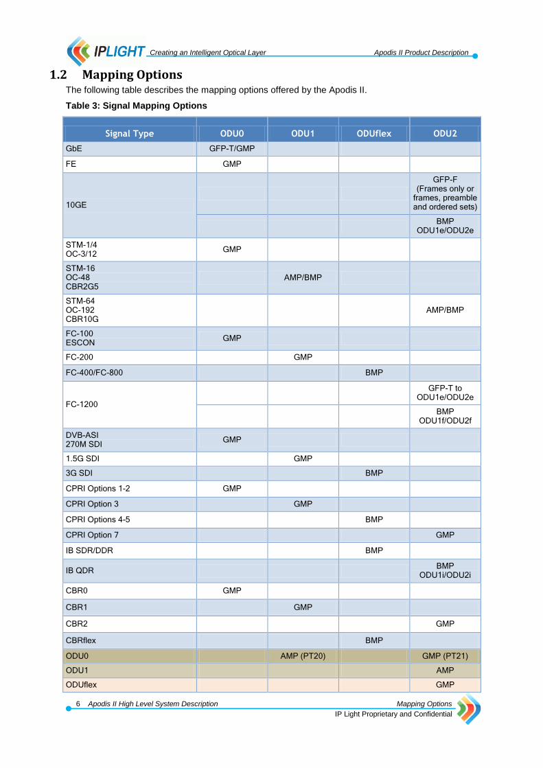
1.2 Mapping Options The following table describes the mapping options offered by the Apodis II.
Table 3: Signal Mapping Options
Signal Type ODU0 ODU1 ODUflex ODU2
GbE GFP-T/GMP
FE GMP
10GE
GFP-F (Frames only or
frames, preamble and ordered sets)
BMP
ODU1e/ODU2e
STM-1/4 OC-3/12
GMP
STM-16 OC-48 CBR2G5
AMP/BMP
STM-64 OC-192 CBR10G
AMP/BMP
FC-100 ESCON
GMP
FC-200 GMP
FC-400/FC-800 BMP
FC-1200
GFP-T to
ODU1e/ODU2e
BMP
ODU1f/ODU2f
DVB-ASI 270M SDI
GMP
1.5G SDI GMP
3G SDI BMP
CPRI Options 1-2 GMP
CPRI Option 3 GMP
CPRI Options 4-5 BMP
CPRI Option 7 GMP
IB SDR/DDR BMP
IB QDR BMP
ODU1i/ODU2i
CBR0 GMP
CBR1 GMP
CBR2 GMP
CBRflex BMP
ODU0 AMP (PT20) GMP (PT21)
ODU1 AMP
ODUflex GMP

Creating an Intelligent Optical Layer Apodis II Product Description
7 Apodis II High Level System Description Mapping Options
IP Light Proprietary and Confidential
These mappings enable non-OTN client signal types to be mapped into the payload of the corresponding ODU according to their relevant rates. In addition, these mappings enable the multiplexing of low order ODUk signals into high order ODUj signals.
The following figure shows the IPL4002M, IPL4102M and IPL4202M client signal to network side port OTN multiplexing and mapping structure.
CBR2G5
OC-48/STM-16
10GE
CBR10G
GFP-F (6.2/7.3)
x1
x8
x1
x1
x1
x1
x1
x1
OPU1 ODU1 OTU1
OPU2 ODU2 OTU2
OPU2e
OPU1e
ODU2e
ODU1e
OTU2e
OTU1e
OPU2f
OPU1f
ODU2f
ODU2f
OTU2f
OTU1f
x4
OPU0ODU0
x2
GFP-T
----------Client---------- --------Network--------
GFP-T
OTU1e/ODU1eOTU2e/ODU2e
OTU2/ODU2
x1
x1
OTU1
x1
FC-200/CPRI 3
OC-3/12; STM-1/4
FE
FC-100/ESCON/CPRI 1-2
3G SDI/CPRI 4-5
OPU2i
OPU1i
ODU2i
ODU2i
OTU2i
OTU1ix1
x1
OPUflex ODUflex
x1
x1
x1
IB QDR
OTU1i/ODU1iOTU2i/ODU2i
1.5G SDI
OTU0
DVB-ASI/270M SDI
GbE
FC-400/800
OC-192/STM-64
IB SDR/DDR
FC-1200
OTU1f/ODU1fOTU2f/ODU2f
x1
x1CPRI Option 7
CBR2x1
CBRflex
CBR0
x1CBR1
Figure 8: IPL4002M, IPL4102M and IPL4202M Network Side Multiplexing and Mapping

Creating an Intelligent Optical Layer Apodis II Product Description
8 Apodis II High Level System Description Mapping Options
IP Light Proprietary and Confidential
The following figure shows the IPL4302F and IPL4402F client signal to network side port OTN multiplexing and mapping structure.
10GE
CBR10G
GFP-F (6.2/7.3)
x1
x1
x1
x1
x1
x1
OPU2 ODU2 OTU2
OPU2e
OPU1e
ODU2e
ODU1e
OTU2e
OTU1e
OPU2f
OPU1f
ODU2f
ODU2f
OTU2f
OTU1f
GFP-T
----------Client---------- --------Network--------
OTU1e/ODU1eOTU2e/ODU2e
OTU2/ODU2
x1
x1
OPU2i
OPU1i
ODU2i
ODU2i
OTU2i
OTU1ix1
x1IB QDR
OTU1i/ODU1iOTU2i/ODU2i
OC-192/STM-64
FC-1200
OTU1f/ODU1fOTU2f/ODU2f
x1
CBR2x1
Figure 9: IPL4302F and IPL4402F Network Side Mapping
Support for GbE is provided by utilizing the GFP-T process, compliant with ITU-T G.7041. The GFP-T process performs transcoding to achieve a rate reduction of the entire Ethernet signal (including IPG, preamble and ordered sets), and reduces the resultant signal rate so that it can be mapped (using a GMP process) into the payload of an ODU0 signal. The clock rate for the GFP-T mapped frame is a derivative of the input Ethernet clock. For more information about ITU-T G.7041 specification, refer to ITU-T G.7041/Y.1303, Generic Framing Procedure (GFP).
Support for 10GE is provided by a GFP-F process to adapt the 10GE signal, with or without preamble and ordered sets, into the payload of an ODU2. The 10GE signal can also be transparently mapped on the payload of an ODU2e/ODU1e signal. For more information about GbE and 10GE signals, see
GbE in Section 2.1.2.6 and 10GE in Section 2.1.2.1.
Storage Area Network (SAN) support includes the following:
FC-100 and ESCON are mapped using GMP into the payload of an ODU0 signal.
FC-200 is mapped using GMP into the payload of an ODU1 signal.
FC-400 and FC-800 are mapped using BMP into the payload of an ODUflex signal.
FC-1200 is rate adapted by utilizing a GFP-T transcoding function and is then mapped into the payload of an ODU1e or ODU2e signal. In addition, the FC-1200 signal can be transparently mapped to the payload of an ODU2f/ODU1f signal.
Video signals support includes the following:
DVB-ASI and 270M SDI are mapped using GMP into the payload of an ODU0 signal
1.5G SDI is mapped using GMP into the payload of an ODU1 signal
3G SDI is mapped using BMP into the payload of an ODUflex signal
CPRI signals support includes the following:
CPRI options 1 and 2 are mapped using GMP into the payload of an ODU0 signal
CPRI option 3 is mapped using GMP into the payload of an ODU1 signal
CPRI options 4 and 5 are mapped using BMP into the payload of an ODUflex signal
CPRI option 7 is mapped using GMP into the payload of an ODU2 signal

Creating an Intelligent Optical Layer Apodis II Product Description
9 Apodis II High Level System Description Mapping Options
IP Light Proprietary and Confidential
Infiniband signals support includes the following:
IB SDR and IB DDR are mapped using BMP into the payload of and ODUflex signal
IB QDR is mapped using BMP into an ODU2i/ODU1i signal
NOTE—OTU2f/2i and OTU1f/1i are non-standard rates. The Apodis II supports all the standard (ITU-T G.709) rates plus several rates that are non-standard, but used in the industry.
The following figure shows the IPL4002M, IPLM4102M and IPL4202M client signal to client side port OTN mapping options.
----------Client---------- ----------Client----------
1.5G SDI
CBR1
10GE
FC-1200
OC-192/STM-64
CBR2
x1
x1
x1
x1
x1
x1
x1
OPU1 ODU1 OTU1
OPU2 ODU2 OTU2
OPU2e
OPU1e
ODU2e
ODU1e
OTU2e
OTU1e
OPU2f
OPU1f
ODU2f
ODU2f
OTU2f
OTU1f
GFP-T
OTU1f/ODU1fOTU2f/ODU2f
x1
OTU1e/ODU1eOTU2e/ODU2e
x1
OTU2/ODU2
x1
OTU1
x1
CBR0
OC-3/12; STM-1/4
x1
x1
ODU0OPU0 OTU0
OTU0
x1
OPU2i
OPU1iODU2i
ODU2i
OTU2i
OTU1ix1
x1IB QDR
OTU1i/ODU1iOTU2i/ODU2i
GbEx1
GFP-T
ESCON; CPRI Options 1/2
DVB-ASI/270M SDI
x1
x1
FEx1
CBR10Gx1
CPRI Option 3x1
CPRI Option 7x1
CBR2G5x1
OC-48/STM-16x1
Figure 10: IPL4002M, IPLM4102M and IPL4202M Client Side Multiplexing and Mapping

Creating an Intelligent Optical Layer Apodis II Product Description
10 Apodis II High Level System Description Cross Connections
IP Light Proprietary and Confidential
The following figure shows the IPL4302F and IPL4402F client signal to client side port OTN mapping options.
----------Client---------- ----------Client----------
10GE
FC-1200
OC-192/STM-64
CBR2x1
x1
x1
x1
x1
OPU2 ODU2 OTU2
OPU2e
OPU1e
ODU2e
ODU1e
OTU2e
OTU1e
OPU2f
OPU1f
ODU2f
ODU2f
OTU2f
OTU1f
GFP-T
OTU1f/ODU1fOTU2f/ODU2f
x1
OTU1e/ODU1eOTU2e/ODU2e
x1
OTU2/ODU2
x1
OPU2i
OPU1iODU2i
ODU2i
OTU2i
OTU1ix1
x1IB QDR
OTU1i/ODU1iOTU2i/ODU2i
CBR10Gx1
Figure 11: IPL4302F and IPL4402F Client Side Multiplexing and Mapping
1.3 Cross Connections
The following table shows the signals that Apodis II supports for client signal to client signal cross connections.
Table 4: Client to Client Cross Connections
GbE FE OC-3/ STM-1
OC-12/ STM-4
OC-48/ STM-16
OC-192/ STM-64
OTU0 OTU1 OTU2
GbE
FE
OC-3/STM-1
OC-12/STM-4
OC-48/STM-16
OC-192/STM-64
OTU0
OTU1
OTU2
The IPL4102M supports client side OTN multiplexing for up to two OTU2 client signals and for up to eight OTU1 client signals. For more information about OTN multiplexing of client signals, see Data
Flow in Section 1.1.

Creating an Intelligent Optical Layer Apodis II Product Description
11 Apodis II High Level System Description Cross Connections
IP Light Proprietary and Confidential
The IPL4102M supports the following client signal to client signal cross connections.
Table 5: IPL4102M Client to Client Cross Connections Including OTN Multiplexing
GbE FE OC-3/ STM-1
OC-12/ STM-4
OC-48/ STM-16
OC-192/ STM-64 OTU0 OTU1 OTU2
GbE
FE
OC-3/STM-1
OC-12/STM-4
OC-48/STM-16
OC-192/STM-64
OTU0
OTU1
OTU2

Creating an Intelligent Optical Layer Apodis II Product Description
12 Apodis II Detailed Description
IP Light Proprietary and Confidential
2 Apodis II Detailed Description Details of the high level blocks are described in the following sections, including:
Client Signal Processor in Section 2.1
Network Signal Processor in Section 2.2
IPLightSERDES™ in Section 2.3
Transparent Agnostic Fabric in Section 2.4
Overhead Access in Section 2.5
Host Processor Interface in Section 2.6
For more information about the Apodis II high level blocks, see Apodis II High Level System
Description in Section 1.
2.1 Client Signal Processor
The Apodis II Client Signal Processor (CSP) supports a variety of signal types, which can be mapped into OTN carrier signals. The CSP is described in the following sections:
Client Signal Processor Block Details in Section 2.1.1
Client Signal Types in Section 2.1.2

Creating an Intelligent Optical Layer Apodis II Product Description
13 Apodis II Detailed Description Client Signal Processor
IP Light Proprietary and Confidential
2.1.1 Client Signal Processor Block Details
There are four Client Signal Processor (CSP) blocks in the IPL4002M, IPL4102M and IPL4302F, and two CSP blocks in the IPL4402F and the IPL4202M.
The following figure shows the CSP for the IPL4002M, IPL4102M and IPL4202M in detail.
Client Signal Processor
High Rate
Se
ria
l/X
AU
I/X
BI2
/SF
I4.2
Se
lecto
r
Se
lecto
r
La
ne
3
Se
lecto
r
SERDES
La
ne
0
SERDES
SERDES
La
ne
2
SERDES
Se
lecto
r
Se
lecto
r
Se
lecto
r
Se
lecto
r
Se
lecto
r
Se
lecto
r
La
ne
1
Se
lecto
r
Se
lecto
r
TAF
OTU0/OTU1
OC-3/12/48; STM-1/4/16; CBR2G5
CBR0/1
FE/GbE
FC-100/200; ESCON
DVB-ASI; 270M/1.5G SDI
CPRI Options 1-3
OTU0/OTU1
OC-3/12/48; STM-1/4/16; CBR2G5
CBR0/1
FE/GbE
FC-100/200; ESCON
DVB-ASI; 270M/1.5G SDI
CPRI Options 1-3
OTU0/OTU1
OC-3/12/48; STM-1/4/16; CBR2G5
CBR0/1
FE/GbE
FC-100/200; ESCON
DVB-ASI; 270M/1.5G SDI
CPRI Options 1-3
OTU0/OTU1
OC-3/12/48; STM-1/4/16; CBR2G5
CBR0/1/flex
FE/GbE
FC-100/200/400/800; ESCON
DVB-ASI; 270M/1.5G/3G SDI
IB SDR/DDR
CPRI Options 1-3, 4-5
10GE (transparent)
FC-1200
FC-1200 (transparent)
10GE GFP-F 6.2/7.3
OC-192/STM-64/CBR10G
OTU2/2e/2f/2i/1e/1f/1i
ODU2/2e/2f/2i/1e/1f/1i
IB QDR
CBR2
CPRI Option 7
Figure 12: IPL4002M, IPL4102M and IPL4202M Client Signal Processor Detailed Block

Creating an Intelligent Optical Layer Apodis II Product Description
14 Apodis II Detailed Description Client Signal Processor
IP Light Proprietary and Confidential
The following figure shows the CSP for the IPL4302F and IPL4402F in detail.
Client Signal Processor
TAFLa
ne
0
SERDES
La
ne
1
SERDES
La
ne
2
SERDES
La
ne
3
SERDES
Se
ria
l/X
AU
I/X
BI2
/SF
I4.2
Se
lecto
r
Se
lecto
r
IB QDR
OTU2/2e/2f/2i/1e/1f/1i
ODU2/2e/2f/2i/1e/1f/1i
CBR2
OC-192/STM-64/CBR10G
10GE (transparent)
10GE GFP-F 6.2/7.3
FC-1200 (transparent)
FC-1200 (GFP-T)
CPRI Option 7
Figure 13: IPL4302F and IPL4402F Client Signal Processor Detailed Block
The CSP may be configured to handle either a single 10 Gbps class client signal or up to four lower rate independent client signals. 10G class may be one of the following signals:
OC-192
STM-64
CBR10G
OTU2
10GE
FC-1200
CPRI Option 7
CBR2
In the four lower rate independent signals mode, lanes 0, 1 and 3 support client signals in the 125 Mbps to 2.5 Gbps range, while lane 2 supports client signals in the 125 Mbps to 8.5 Gbps range.
When configured in the single 10 Gbps class client signal mode, the CSP block may be configured to operate across one of the following interfaces:
Single lane serial interface
XBI2 interface
XAUI interface
SFI4.2 interface
For more information about the XBI2 and SFI4.2 interfaces, see XBI2 Interface in Section 2.3.4.2 and
SFI4.2 Interface in Section 2.3.4.4.

Creating an Intelligent Optical Layer Apodis II Product Description
15 Apodis II Detailed Description Client Signal Processor
IP Light Proprietary and Confidential
2.1.2 Client Signal Types
The following sections describe the client to network cross-connection options supported by the Apodis II Client Signal Processor (CSP). Client to client cross-connections are handled in a similar way where applicable.
10GE in Section 2.1.2.1
FC-1200 in Section 2.1.2.2
OTU2/ODU2 in Section 2.1.2.3
OTU1 in Section 2.1.2.4
OTU0 in Section 2.1.2.5
GbE in Section 2.1.2.6
FE in Section 2.1.2.7
FC-100 in Section 2.1.2.8
ESCON in Section 2.1.2.9
FC-200 in Section 2.1.2.10
FC-400 and FC-800 in Section 2.1.2.11
OC-192/STM-64 and CBR10G in Section 2.1.2.12
OC-48/STM-16 and CBR2G5 in Section 2.1.2.13
OC-3/STM-1 and OC-12/STM-4 in Section 2.1.2.14
CPRI Options 1 and 2 in Section 2.1.2.15
CPRI Option 3 in Section 2.1.2.16
CPRI Options 4 and 5 in Section 2.1.2.17
CPRI Option 7 in Section 2.1.2.18
DVB-ASI in Section 2.1.2.19
270M SDI in Section 2.1.2.20
1.5G SDI in Section 2.1.2.21
3G SDI in Section 2.1.2.22
IB SDR and DDR in Section 2.1.2.23
IB QDR in Section 2.1.2.24
CBR0 in Section 2.1.2.25
CBR1 in Section 2.1.2.26
CBR2 in Section 2.1.2.27
CBRflex in Section 2.1.2.28

Creating an Intelligent Optical Layer Apodis II Product Description
16 Apodis II Detailed Description Client Signal Processor
IP Light Proprietary and Confidential
2.1.2.1 10GE
The following figure shows how 10GE signals are connected, either through a serial interface or through a XAUI interface.
GFP-F(supp. 43 - 6.2/7.3)
OPU2 ODU2 OTU2
OPU2eOPU1e
ODU2eODU1e
OTU2eOTU1e
PCS
MAC
RMON
Monitor
10GE
XAUI
Se
lect
Se
lect
Monitor
Network sideClient side
Figure 14: 10GE Processing
When using XAUI the signal is converted into XGMII, which is either further processed by GFP-F or further converted into 64B/66B blocks for transparent transport mode operation. When using a serial interface the signal is connected to the 10GE PCS.
10GE mapping into OTN through a GFP-F process is implemented according to the ITU-T standard. The option is provided to use GFP-F to encapsulate just the data or to encapsulate the data, preamble, and ordered sets. GFP-F idle frames are used to rate-adapt the signal to the OPU2 rate. The GFP-F frames can be mapped exclusively into the OPU2 payload or they may also use the reserved bytes in the OPU2 overhead (GFP Extended mode). For more information about the ITU-T standard, refer to ITU-T Series G Supplement 43, Transport of IEEE 10G base-R in optical transport networks (OTN), Sections 6.2 and 7.3.
Transparent transport mode is used to encapsulate the entire 10GE signal into an OTU2e/OTU1e signal. In this case, the OTU2e/1e signal timing is synchronized to the 10GE signal timing.
The 10GE signals are monitored for alarms and indications. Various mechanisms are also provided for performance monitoring of transmitted signals.
The Apodis II provides transmit and receive signal counters to support RMON Ethernet statistics as specified in IETF RFC 2819, Remote Network Monitoring MIB.
NOTE—In the Tx direction Apodis II provides a subset of the RMON statistics.
The following table describes the 10GE signal rates for both serial and XAUI interfaces.
Table 6: 10GE Client Interface Signal Rate
Interface Serial (Gbps) --Per Lane-- XAUI (Gbps)
10GE 10.313 (±100ppm) 3.125 (±100ppm)
For the 10GE serial interface, a special type of PCS test can be conducted, conforming to IEEE 802.3. Using two user-defined seeds, this test loads the line-code scrambler with a new seed every 128 blocks. The data is either 64 zeros or the 64 bit encoding for local fault ordered sets, which can be monitored on the receive interface.
Additional PCS tests include generation of a PRBS31 test signal or an optional square wave. For more information about generating test signals, see Pseudo-random Binary Sequences in Section
2.3.2.2.
Creating an Intelligent Optical Layer Apodis II Product Description
17 Apodis II Detailed Description Client Signal Processor
IP Light Proprietary and Confidential
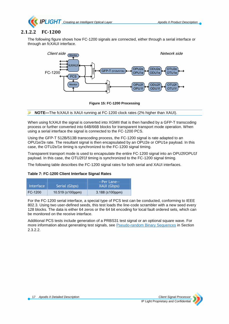
2.1.2.2 FC-1200
The following figure shows how FC-1200 signals are connected, either through a serial interface or through an fcXAUI interface.
GFP-T (512b/513b)OPU2e
OPU1e
ODU2e
ODU1e
OTU2e
OTU1e
OPU2f
OPU1f
ODU2f
ODU1f
OTU2f
OTU1f
PCS
Monitor
fcXAUI
Se
lect
Se
lect
Monitor
FC-1200
Network sideClient side
Figure 15: FC-1200 Processing
NOTE—The fcXAUI is XAUI running at FC-1200 clock rates (2% higher than XAUI).
When using fcXAUI the signal is converted into XGMII that is then handled by a GFP-T transcoding process or further converted into 64B/66B blocks for transparent transport mode operation. When using a serial interface the signal is connected to the FC-1200 PCS.
Using the GFP-T 512B/513B transcoding process, the FC-1200 signal is rate adapted to an OPU1e/2e rate. The resultant signal is then encapsulated by an OPU2e or OPU1e payload. In this case, the OTU2e/1e timing is synchronized to the FC-1200 signal timing.
Transparent transport mode is used to encapsulate the entire FC-1200 signal into an OPU2f/OPU1f payload. In this case, the OTU2f/1f timing is synchronized to the FC-1200 signal timing.
The following table describes the FC-1200 signal rates for both serial and XAUI interfaces.
Table 7: FC-1200 Client Interface Signal Rates
Interface Serial (Gbps) --Per Lane-- XAUI (Gbps)
FC-1200 10.519 (±100ppm) 3.188 (±100ppm)
For the FC-1200 serial interface, a special type of PCS test can be conducted, conforming to IEEE 802.3. Using two user-defined seeds, this test loads the line-code scrambler with a new seed every 128 blocks. The data is either 64 zeros or the 64 bit encoding for local fault ordered sets, which can be monitored on the receive interface.
Additional PCS tests include generation of a PRBS31 test signal or an optional square wave. For more information about generating test signals, see Pseudo-random Binary Sequences in Section
2.3.2.2.

Creating an Intelligent Optical Layer Apodis II Product Description
18 Apodis II Detailed Description Client Signal Processor
IP Light Proprietary and Confidential
2.1.2.3 OTU2/ODU2
The following figure shows how on the client side, the Apodis II can be configured for OTU2 or ODU2 signals.
ODU2 OTU2
OTU2
Network sideClient side
Se
lecto
r
SFI4.2
XBI2-4
XBI2-2
OTU2/ODU2
Figure 16: OTU2 Processing
The client port can be configured for serial (XFI), two-lane XBI2-2, four-lane XBI2-4 or SFI4.2 interface operation. For more information about the XBI2 and SFI4.2 interface operations, see XBI2
Interface in Section 2.3.4.2 and SFI4.2 Interface in Section 2.3.4.4.
The OTU2 signals are terminated and then processed in either path or tandem mode. In either mode, errors are detected and corrected according to the GFEC and support is also provided for up to six layers of TCM. In path mode, the OPU2 payload is extracted. For tandem mode, the ODU2 is passed through, while monitoring the ODU2 signal and the corresponding TCMs. For more information about
TCM, see Tandem Connection Monitoring in Section 3.1.2.
For the client side OTU2, the client signal carried by the OPU2 may be recovered and presented in its native format back to one of the client side ports. The CSP also supports OTN tandem connections in between client side OTU2 ports (meaning, transmitting their respective ODU2 signals through another client side OTU2 port).
The ODU2 signal overhead is monitored, and may be modified. For more information about overhead
access, see Overhead Access in Section 2.5.
The OTN signal is monitored for alarms and indications as specified by ITU-T G.798. For more information about alarms and indications, see OTN Alarms and Indications.
SF and SD indications are provided at all OTN levels (SM/PM/TCM).
Various mechanisms are also provided for performance monitoring and OTN network maintenance tests are also provided. For more information about performance monitoring and maintenance, see
OTN Performance Monitoring in Section 3.1 and OTN Maintenance in Section 2.2.2.1.2.
The following table describes the OTU2/ODU2 signal rates for both serial, XBI2 and SFI4.2 interfaces.
Table 8: OTU2/ODU2 Client Interface Signal Rates
Interface Serial (Gbps)
----------------------Per Lane----------------------
XBI2-4 (Gbps) XBI2-2 (Gbps) SFI4.2 (Gbps)
ODU2 10.037 (± 20ppm) 2.509 (± 20ppm) 5.019 (± 20ppm) 2.587 (± 20ppm)
ODU1e 10.356 (±100ppm) 2.589 (±100ppm) 5.178 (±100ppm) 2.670 (±100ppm)
ODU2e 10.400 (±100ppm) 2.600 (±100ppm) 5.200 (±100ppm) 2.681 (±100ppm)
ODU1f 10.563 (±100ppm) 2.641 (±100ppm) 5.282 (±100ppm) 2.723 (±100ppm)
ODU2f 10.608 (±100ppm) 2.652 (±100ppm) 5.304 (±100ppm) 2.735 (±100ppm)

Creating an Intelligent Optical Layer Apodis II Product Description
19 Apodis II Detailed Description Client Signal Processor
IP Light Proprietary and Confidential
Interface Serial (Gbps)
----------------------Per Lane----------------------
XBI2-4 (Gbps) XBI2-2 (Gbps) SFI4.2 (Gbps)
ODU1i 10.042 (±100ppm) 2.511 (±100ppm) 5.021 (±100ppm) 2.589 (±100ppm)
ODU2i 10.084 (±100ppm) 2.521 (±100ppm) 5.042 (±100ppm) 2.600 (±100ppm)
OTU2 10.709 (± 20ppm) 2.677 (± 20ppm) 5.355 (± 20ppm) 2.761 (± 20ppm)
OTU1e 11.049 (±100ppm) 2.762 (±100ppm) 5.525 (±100ppm) 2.849 (±100ppm)
OTU2e 11.096 (±100ppm) 2.774 (±100ppm) 5.548 (±100ppm) 2.861 (±100ppm)
OTU1f 11.270 (±100ppm) 2.818 (±100ppm) 5.635 (±100ppm) 2.906 (±100ppm)
OTU2f 11.318 (±100ppm) 2.829 (±100ppm) 5.660 (±100ppm) 2.918 (±100ppm)
OTU1i 10.714 (±100ppm) 2.679 (±100ppm) 5.357 (±100ppm) 2.762 (±100ppm)
OTU2i 10.760 (±100ppm) 2.690 (±100ppm) 5.380 (±100ppm) 2.774 (±100ppm)
2.1.2.4 OTU1
The following figure shows how OTU1 signals are cross-connected to the network side.
OTU1 ODU1
OPU2 ODU2 OTU2x4
OTU1
Network sideClient side
OTU1
Figure 17: OTU1 Processing
OTU1 signals received on the client side are terminated, and then errors can be detected and corrected according to the GFEC. The ODU1, including up to six levels of TCM, can be monitored, and then the ODU1 signal is cross-connected to a Client/Line Side OTU1 or multiplexed on the network side into an OPU2. For IPL4202M the ODU1 can be cross-connected to an OTU1 network interface (Tandem). For more information about TCM, see Tandem Connection Monitoring in Section
3.1.2.
In addition, an ODU1 extracted from a client side OTU1 can be further processed on the client side. Some client signals can be extracted from the OPU1 and presented in their native format back to one of the client side ports.
For information about overhead access, see Overhead Access in Section 2.5.
The OTU1 signals are monitored for alarms and indications. For more information about alarms and
indications, see OTN Alarms and Indications in Section 3.2.
In addition, SF and SD indications can be provided at all OTN levels (SM/PM/TCM).
Various mechanisms are also provided for performance monitoring and OTN network maintenance testing. For more information about performance monitoring and maintenance testing, see OTN
Maintenance in Section 2.2.2.1.2 and OTN Performance Monitoring in Section 3.1.
The following table describes the OTU1 signal rate.
Table 9: OTU1 Client Interface Signal Rate
Interface Serial (Gbps)
OTU1 2.677 (±20ppm)

Creating an Intelligent Optical Layer Apodis II Product Description
20 Apodis II Detailed Description Client Signal Processor
IP Light Proprietary and Confidential
2.1.2.5 OTU0
The following figure shows how OTU0 signals are multiplexed into the network side.
OTU0 ODU0x2
x8
OTU0
Network sideClient side
OPU1 ODU1
OPU2 ODU2 OTU2
x4
OTU1
Figure 18: OTU0 Processing
OTU0 signals received on the client side are terminated, and then errors can be detected and corrected according to the GFEC. The ODU0, including up to six TCM levels, can be monitored. The ODU0 is then either AMP mapped into an OPU1 or it can be GMP mapped into an ODTU02, which is used to fill one of the eight 1.25G tributary slots of an OPU2. For IPL4202M, the OPU1 can also be mapped into an OTU1 signal. For more information about TCM, see Tandem Connection Monitoring
in Section 3.1.2.
For information about overhead access, see Overhead Access in Section 2.5.
The OTU0 signals can be monitored for alarms and indications. For more information about alarms
and indications, see OTN Alarms and Indications in Section 3.2.
In addition, SF and SD indications can be provided at all OTN levels (SM/PM/TCM).
Various mechanisms are also provided for performance monitoring and OTN network maintenance testing. For more information about performance monitoring and maintenance testing, see OTN
Maintenance in Section 2.2.2.1.2 and OTN Performance Monitoring in Section 3.1.
The following table describes the OTU0 signal rate.
Table 10: OTU0 Client Interface Signal Rate
Interface Serial (Gbps)
OTU0 1.328 (±20ppm)
2.1.2.6 GbE
Gigabit Ethernet (GbE) uses an 8B/10B line code which is terminated in the PCS block. The following figure shows how GbE signals are processed.
MAC
RMON
OPU1 ODU1
OPU0 ODU0GFP-T (64b/66b)
GbE
x2
x8
x4
OPU2 ODU2 OTU2
PCS
Network sideClient side
Monitor
OTU1
Figure 19: GbE Processing

Creating an Intelligent Optical Layer Apodis II Product Description
21 Apodis II Detailed Description Client Signal Processor
IP Light Proprietary and Confidential
Using GFP-T, the whole GbE signal, including preamble and IPG symbols, is transcoded from 8B/10B to 64B/65B line-code and then GMP mapped into an OPU0 payload. The ODU0 is then either AMP mapped into an OPU1 or it can be GMP mapped into an ODTU02, which is used to fill one of the eight tributary slots of an OPU2. For IPL4202M, the OPU1 can also be mapped into an OTU1 signal.
The GbE signal clock is transparently transported, providing support for synchronous Ethernet applications.
Support of transmission and reception of OAM frames is provided to detect and generate OAM frames for any Layer 2 protocol. The following are examples of supported Layer 2 protocols:
Link layer OAM
Carrier Ethernet OAM
Packet Timing Protocol
In addition, detected OAM frames may include several VLAN and MPLS tags.
The following figure shows the OAM functionality.
OAM Rx D3BufferOAM Rx D2
BufferOAM Rx D1Buffer
OAM Rx U3BufferOAM Rx U2
BufferOAM Rx U1Buffer
OAM Tx DBuffer
OAM Tx UBuffer
GbE OTN
Figure 20: OAM Functions
On the receive sides (from the GbE port or from the OTN network), if the incoming frame matches the detection mask of one of the three OAM Rx buffers, then it is stored in that OAM Rx buffer. This buffer sets a flag once the entire frame has been received. The host processor detects this flag and reads out the OAMPDU. The user software can then take appropriate actions based on the information received, such as creating an internal loopback as shown by the dotted line in the figure above. The user software can also transmit information to the GbE port or to the OTN network, by writing an OAMPDU to the corresponding OAM Tx buffer. When a complete frame is written, the data is multiplexed with the information transmit data. Transmit and receive time of OAM frames is recorded to allow the user implementation of the IEEE 1588v2 PTP protocol.
Apodis II provides all the functions required to implement the data link layer remote loopback mode, as defined in IEEE 802.3 section 57, under user software control. This mode can be used for link monitoring and diagnostics.
The GbE signals are monitored in both directions (Rx—from the client signal, Tx—from an OTN bearer) for alarms and indications. Various mechanisms are also provided for performance monitoring of transmitted signals.
Apodis II provides counters to support RMON Ethernet statistics as specified in IETF RFC 2819, Remote Network Monitoring MIB. In addition, EPORT statistics are also supported.
NOTE—In the Tx direction Apodis II provides a subset of RMON statistics.
The following table describes the GbE signal rate for a serial interface.
Table 11: GbE Client Interface Signal Rate
Interface Serial (Gbps)
GbE 1.250 (±100ppm)

Creating an Intelligent Optical Layer Apodis II Product Description
22 Apodis II Detailed Description Client Signal Processor
IP Light Proprietary and Confidential
2.1.2.7 FE
The following figure shows how FE signals are processed.
ODU0x2
x8 OPU2 ODU2 OTU2
FE OPU1 ODU1
x4
Network sideClient side
OPU0 OTU1
Figure 21: FE Processing
In the receive direction the entire FE signal, including preamble and IPG symbols, is GMP mapped into an OPU0 payload. The ODU0 is then either AMP mapped into an OPU1 or it can be GMP mapped into an ODTU02, which is used to fill one of the eight tributary slots of an OPU2. The FE clock is transparently transported. For IPL4202M, the OPU1 can also be mapped into an OTU1 signal.
The following table describes the FE signal rate for a serial interface.
Table 12: FE Client Interface Signal Rate
Interface Serial (Gbps)
FE 0.125 (±100ppm)
2.1.2.8 FC-100
The following figure shows how One Gigabit Fibre Channel (FC-100) signals are handled.
OPU1 ODU1
OPU2 ODU2 OTU2
OPU0 ODU0
x2
x8x4FC-100 PCS
Monitor
Network sideClient side
OTU1
Figure 22: FC-100 Processing
The FC-100 signals are mapped using GMP into an OPU0 payload. The ODU0 is then either AMP mapped into an OPU1 (carrying up to two ODU0 signals) or it can be GMP mapped into an ODTU02, which is used to fill one of the eight tributary slots of an OPU2. For IPL4202M, the OPU1 can also be mapped into an OTU1 signal.
The FC-100 signals are monitored for alarms and indications. Various mechanisms are also provided for performance monitoring.
The following table describes the FC-100 signal rate for a serial interface.
Table 13: FC-100 Client Interface Signal Rate
Interface Serial (Gbps)
FC-100 1.063 (±100ppm)

Creating an Intelligent Optical Layer Apodis II Product Description
23 Apodis II Detailed Description Client Signal Processor
IP Light Proprietary and Confidential
2.1.2.9 ESCON
The following figure shows how Enterprise Systems CONnection (ESCON) signals are handled.
ODU0x2
x8 OPU2 ODU2 OTU2
ESCON OPU1 ODU1
x4
PCS
Network sideClient side
OPU0
Monitor
OTU1
Figure 23: ESCON Processing
The ESCON signals are mapped using GMP into an OPU0 payload. The ODU0 is then either AMP mapped into an OPU1 (carrying up to two ODU0 signals) or it can be GMP mapped into an ODTU02, which is used to fill one of the eight tributary slots of an OPU2. For IPL4202M, the OPU1 can also be mapped into an OTU1 signal.
The ESCON signals are monitored for alarms and indications. Various mechanisms are also provided for performance monitoring.
The following table describes the ESCON signal rate for a serial interface.
Table 14: ESCON Client Interface Signal Rate
Interface Serial (Gbps)
ESCON 0.270 (±200 ppm)
2.1.2.10 FC-200
The following figure shows how Two Gigabit Fibre Channel (FC-200) signals are handled.
Client side
OPU1 ODU1FC-200 PCS
Monitor
Network side
OPU2 ODU2 OTU2x4
OTU1
Figure 24: FC-200 Processing
The FC-200 signals are mapped using GMP into an OPU1 payload. The ODU1 is then AMP mapped into an OPU2. For IPL4202M, the OPU1 can also be mapped into an OTU1 signal.
The FC-200 signals are monitored for alarms and indications. Various mechanisms are also provided for performance monitoring.
The following table describes the FC-200 signal rate for a serial interface.
Table 15: FC-200 Client Interface Signal Rate
Interface Serial (Gbps)
FC-200 2.125 (±100 ppm)

Creating an Intelligent Optical Layer Apodis II Product Description
24 Apodis II Detailed Description Client Signal Processor
IP Light Proprietary and Confidential
2.1.2.11 FC-400 and FC-800
The following figure shows how Four and Eight Gigabit Fibre Channel (FC-400/800) signals are handled.
OPUflexFC-400FC-800 PCS
Network sideClient side
ODUflex OPU2 ODU2 OTU2
Figure 25: FC-400 and FC-800 Processing
The FC-400 and FC-800 signals are mapped using BMP into an OPUflex payload. The ODUflex is then GMP mapped into an OPU2. FC-400 occupies four OPU2 time slots, while FC-800 occupies seven.
The following table describes the FC-400 and FC-800 signal rates for a serial interface.
Table 16: FC-400 and FC-800 Client Interface Signal Rates
Interface Serial (Gbps)
FC-400 4.250 (±100 ppm)
FC-800 8.500 (±100 ppm)
2.1.2.12 OC-192/STM-64 and CBR10G
The following figure shows how an OC-192/STM-64/CBR10G signal is handled.
OPU2 ODU2 OTU2Section/RegeneratorLine/Multiplexor
Network sideClient side
Se
lecto
rSFI4.2Section/Regenerator
Line/Multiplexor
OC-192/STM-64
CBR10G
Figure 26: OC-192/STM-64/CBR10G Processing
For BMP the OTU2 clock is a derivative of the OC-192 clock. The signal may also be processed in transparent transport mode, which sends the received signal directly through without any modification. In transparent transport mode, the signal is monitored for the corresponding alarms and indications. The client port may be configured to serial or four lane SFI4.2.
In the receive direction, the Apodis II synchronizes to the OC 192/STM 64 signal. Once synchronization is achieved, the section overhead is monitored as follows:
B1 is monitored for BIP errors
J0 is monitored for the section trace message
The line overhead is also monitored as follows:
B2 is monitored for BIP errors and SF/SD
M0/M1 are monitored for remote errors
K2 byte is monitored for AIS and RDI
K1/K2 and the S1 bytes are captured and made available to the user
The Section and Line header fields can be regenerated and the RDI alarm can be generated before being mapped to the OPU2.

Creating an Intelligent Optical Layer Apodis II Product Description
25 Apodis II Detailed Description Client Signal Processor
IP Light Proprietary and Confidential
In the transmit direction, the Apodis II synchronizes to the OC 192/STM 64 signal recovered from the OPU2. Once synchronization is achieved, the section overhead is monitored as follows:
B1 is monitored for BIP errors
The line overhead is also monitored as follows:
B2 is monitored for BIP errors and SF/SD
M0/M1 are monitored for remote errors
K2 byte is monitored for AIS and RDI
K1/K2 and the S1 bytes are captured and made available to the user
AIS and RDI alarms can be generated if required, and the B1, J0, B2, M0/M1, S1 and K1/K2 bytes may be added to the signal, which is then transmitted out of the CSP.
The E1/E2, F1 and DCC overhead bytes from the signal received in the client interface or from the signal demapped from the OPU2 are available to the user through the external overhead interface.
For more information about the EOI, see External Overhead Interface in Section 2.5.1.
For CBR10G signals, the SONET/SDH specific blocks are bypassed.
The following table describes the OC-192/STM-64/CBR10G signal rates.
Table 17: OC-192/STM-64/CBR10G Client Interface Signal Rates
Interface Serial (Gbps)
SFI4.2 (Gbps) Per lane
OC-192/STM-64/CBR10G 9.953 (±20ppm) 2.566 (±20 ppm)
For the OC-192/STM-64 signal, the following SONET/SDH network maintenance tests are supported:
PRBS31 testing
PRBS31 testing is implemented as defined in ITU-T G.707. This test loads any SONET/SDH signal payload within the Apodis II with a PRBS31. On the receive side, monitoring of the PRBS31 signal is provided and when an error is detected in the received PRBS31 the errors are counted.
Signal Impair
Signal Impair is a proprietary test function, which operates on one byte of a SONET/SDH frame. The test signal insertion occurs before the scrambler. The byte selected is replaced with a user-defined byte or using an XOR gate with the user-defined byte. Additionally, the rate of the test signal insertion can be configured to be single, burst, continuous, or periodical.
2.1.2.13 OC-48/STM-16 and CBR2G5
The following figure shows how OC-48/STM-16 signals are handled.
OPU2 ODU2 OTU2
Network sideClient side
OPU1 ODU1
Section/Regenerator
Line/Multiplexor
Section/Regenerator
Line/Multiplexor
OC-48/STM-16
OTU1
Figure 27: OC-48/STM-16 Processing
OC48/STM16 signals may be transported transparently by ODU1 containers, without modification. In transparent mode, the OC48/STM16 signals can still be monitored for the corresponding alarms and section level indications.

Creating an Intelligent Optical Layer Apodis II Product Description
26 Apodis II Detailed Description Client Signal Processor
IP Light Proprietary and Confidential
In the client receive direction the Apodis II synchronizes to the incoming OC 48/STM 16 signal. Once synchronization is achieved, the section overhead can be monitored as follows:
B1 is monitored for BIP errors
J0 is monitored for the section trace message
The line overhead can also be monitored as follows:
B2 is monitored for BIP errors and SF/SD
M0/M1 are monitored for remote errors
K2 byte is monitored for AIS and RDI
K1/K2 and the S1 bytes are captured and made available to the user
The Section and Line header fields can be regenerated and the RDI alarm can be generated before being mapped to the OPU1 bearer.
In the client transmit direction the Apodis II synchronizes to the OC-48/STM-16 signal recovered from the OPU1. Once synchronization is achieved, the section overhead can be monitored as follows:
B1 is monitored for BIP errors
The line overhead can also be monitored as follows:
B2 is monitored for BIP errors and SF/SD
M0/M1 are monitored for remote errors
K2 byte is monitored for AIS and RDI
K1/K2 and the S1 bytes are captured and made available to the user
AIS and RDI alarms can be generated if required, and the B1, J0, B2, M0/M1, S1 and K1/K2 bytes may be added to the signal, which is then transmitted out of the CSP.
The E1/E2, F1 and DCC overhead bytes from the OC-48/STM-16 signal received in the client interface or from the OC-48/STM-16 signal demapped from the OPU1 bearer are available through the external overhead interface. For more information about EOI, see External Overhead Interface in
Section 2.5.1.
SONET/SDH network maintenance tests are also provided.
For CBR2G5 signals, the SONET/SDH specific blocks are bypassed.
The following table describes the OC-48/STM-16/CBR2G5 signal rate.
Table 18: OC-48/STM-16/CBR2G5 Client Interface Signal Rate
Interface Serial (Gbps)
OC-48/STM-16/CBR2G5 2.488 (±20 ppm)
2.1.2.14 OC-3/STM-1 and OC-12/STM-4
The following figure shows how the OC-3/STM-1 and OC-12/STM-4 signals are handled.
ODU0x2
x8 OPU2 ODU2 OTU2
OC-3/STM-1OC-12/STM-4 OPU1 ODU1
x4
Network sideClient side
OPU0Section/
RegeneratorLine/
Multiplexor
Section/Regenerator
Line/Multiplexor
OTU1
Figure 28: OC-3/STM-1 and OC-12/STM-4 Processing

Creating an Intelligent Optical Layer Apodis II Product Description
27 Apodis II Detailed Description Client Signal Processor
IP Light Proprietary and Confidential
In the client receive direction, the Apodis II synchronizes to the OC-3/STM-1 or OC-12/STM-4 signals. Once synchronization is achieved, the section overhead can be monitored for the following:
B1 is monitored for BIP errors
J0 is monitored for the section trace message
The line overhead can also be monitored for the following:
B2 is monitored for BIP errors and SF/SD
M0/M1 are monitored for remote errors
K2 byte is monitored for AIS and RDI
K1/K2 and the S1 bytes are captured and made available to the user
In the client transmit direction the Apodis II synchronizes to the OC-3/STM-1 or OC-12/STM-4 signals recovered from their respective OPU0 bearers. Once synchronization is achieved, the section overhead can be monitored for the following:
B1 is monitored for BIP errors
The line overhead can also be monitored for the following:
B2 is monitored for BIP errors and SF/SD
M0/M1 are monitored for remote errors
K2 byte is monitored for AIS and RDI
K1/K2 and the S1 bytes are captured and made available to the user
AIS and RDI alarms can be generated if required, and the B1, J0, B2, M0/M1, S1 and K1/K2 bytes may be added to the OC-3/STM-1 or OC-12/STM-4 signal, which is then transmitted out of the CSP.
The E1/E2, F1 and DCC overhead bytes from the OC-3/STM-1 or OC-12/STM-4 signal received in the client interface or from the OC-3/STM-1 or OC-12/STM-4 signal demapped from the OPU0 bearer are available through the external overhead interface. For more information about EOI, see External
Overhead Interface in Section 2.5.1.
The OC-3/STM-1 or OC-12/STM-4 signals are mapped using GMP into an OPU0 payload. The ODU0 is then either AMP mapped into an OPU1 (carrying up to two ODU0 signals) or it can be GMP mapped into an ODTU02, which is used to fill one of the eight tributary slots of an OPU2. For IPL4202M, the OPU1 can also be mapped into an OTU1 signal.
SONET/SDH network maintenance tests are also provided.
The following table describes the OC-3/STM-1 and OC-12/STM-4 signal rates.
Table 19: OC-3/STM-1 and OC-12/STM-4 Client Interface Signal Rates
Interface Serial (Gbps)
OC-3/STM-1 0.15552 (±20 ppm)
OC-12/STM-4 0.62208 (±20 ppm)

Creating an Intelligent Optical Layer Apodis II Product Description
28 Apodis II Detailed Description Client Signal Processor
IP Light Proprietary and Confidential
2.1.2.15 CPRI Options 1 and 2
The following figure shows how the CPRI Options 1 and 2 signals are handled.
ODU0x2
x8 OPU2 ODU2 OTU2
CPRIOptions 1 & 2
OPU1 ODU1
x4
PCS
Network sideClient side
OPU0
Monitor
OTU1
Figure 29: CPRI Options 1 and 2 Processing
The CPRI Options 1 and 2 signals are mapped using GMP into an OPU0 payload. The ODU0 is then either AMP mapped into an OPU1 (carrying up to two ODU0 signals) or it can be GMP mapped into an ODTU02, which is used to fill one of the eight tributary slots of an OPU2. For IPL4202M, the OPU1 can also be mapped into an OTU1 signal.
The CPRI Options 1 and 2 signals are monitored for alarms and indications. Various mechanisms are also provided for performance monitoring.
The following table describes the CPRI Options 1 and 2 signal rate.
Table 20: CPRI Options 1 and 2 Client Interface Signal Rates
Interface Serial (Gbps)
CPRI Option 1 0.6144 (±100 ppm)
CPRI Option 2 1.2288 (±100 ppm)
2.1.2.16 CPRI Option 3
The following figure shows how CPRI Option 3 signals are handled.
OPU2 ODU2 OTU2CPRI Option 3 OPU1 ODU1x4
PCS
Network sideClient side
Monitor
OTU1
Figure 30: CPRI Option 3 Processing
The CPRI Option 3 signal is mapped using GMP into an OPU1 payload. The ODU1 is then AMP mapped into an OPU2. For IPL4202M, the OPU1 can also be mapped into an OTU1 signal.
The CPRI Option 3 signal can be monitored for alarms and indications. Various mechanisms are also provided for performance monitoring.
The following table describes the CPRI Option 3 signal rate.
Table 21: CPRI Option 3 Client Interface Signal Rate
Interface Serial (Gbps)
CPRI Option 3 2.4576 (±100 ppm)

Creating an Intelligent Optical Layer Apodis II Product Description
29 Apodis II Detailed Description Client Signal Processor
IP Light Proprietary and Confidential
2.1.2.17 CPRI Options 4 and 5
The following figure shows how the CPRI Options 4 and 5 signals are handled.
OPU2 ODU2 OTU2CPRI Options 4&5 OPUflex ODUflexPCS
Network sideClient side
Figure 31: CPRI Options 4 and 5 Processing
The CPRI Options 4 and 5 signals are mapped using BMP into an OPUflex payload. The ODUflex is then GMP mapped into an OPU2. CPRI Option 4 occupies three OPU2 1.25G time slots, while CPRI Option 5 occupies four 1.25G time slots.
The following table describes the CPRI Options 4 and 5 signal rates.
Table 22: CPRI Options 4 and 5 Client Interface Signal Rates
Interface Serial (Gbps)
CPRI Option 4 3.072 (±100 ppm)
CPRI Option 5 4.9152 (±100 ppm)
2.1.2.18 CPRI Option 7
The following figure shows how CPRI Option 7 signals are handled.
OPU2 ODU2 OTU2CPRI Option 7 PCS
Network sideClient side
Figure 32: CPRI Option 7 Processing
The CPRI Option 7 signals are mapped using GMP into an OPU2 payload.
The following table describes the CPRI Option 7 signal rate for a serial interface.
Table 23: CPRI Option 7 Client Interface Signal Rate
Interface Serial (Gbps)
CPRI Option 7 9.8304 (±100 ppm)
2.1.2.19 DVB-ASI
The following figure shows how DVB-ASI signals are handled.
ODU0x2
x8 OPU2 ODU2 OTU2
DVB-ASI OPU1 ODU1
x4
PCS
Network sideClient side
OPU0
Monitor
OTU1
Figure 33: DVB-ASI Processing

Creating an Intelligent Optical Layer Apodis II Product Description
30 Apodis II Detailed Description Client Signal Processor
IP Light Proprietary and Confidential
In the receive direction the entire DVB-ASI signal is mapped using GMP into an OPU0 payload. The ODU0 is then either AMP mapped into an OPU1 or it can be GMP mapped into an ODTU02, which is used to fill one of the eight 1.25G tributary slots of an OPU2. For IPL4202M, the OPU1 can also be mapped into an OTU1 signal.
The DVB-ASI signals are monitored for alarms and indications. Various mechanisms are also provided for performance monitoring.
The following table describes the DVB-ASI signal rate.
Table 24: DVB-ASI Client Interface Signal Rate
Interface Serial (Gbps)
DVB-ASI 0.270 (±100 ppm)
2.1.2.20 270M SDI
The following figure shows how 270M SDI signals are handled.
ODU0x2
x8 OPU2 ODU2 OTU2
270M SDI OPU1 ODU1
x4
NRZI
Network sideClient side
OPU0 OTU1
Figure 34: 270M SDI Processing
In the receive direction the entire 270M SDI signal is mapped using GMP into an OPU0 payload. The ODU0 is then either AMP mapped into an OPU1 or it can be GMP mapped into an ODTU02, which is used to fill one of the eight 1.25G tributary slots of an OPU2. For IPL4202M, the OPU1 can also be mapped into an OTU1 signal.
The 270M SDI signals are monitored for alarms and indications.
The following table describes the 270M SDI signal rate for a serial interface.
Table 25: 270M SDI Client Interface Signal Rate
Interface Serial (Gbps)
270M SDI 0.270 (±2.8 ppm)
2.1.2.21 1.5G SDI
The following figure shows how 1.5G SDI signals are handled.
1.5G SDI OPU1 ODU1NRZI
Network sideClient side
OTU1
OPU2 ODU2 OTU2x4
Figure 35: 1.5G SDI Processing
The 1.5G SDI signals are mapped using GMP into an OPU1 payload. The ODU1 is then AMP mapped into an OPU2. For IPL4202M, the OPU1 can also be mapped into an OTU1 signal.
The 1.5G SDI signals are monitored for alarms and indications.

Creating an Intelligent Optical Layer Apodis II Product Description
31 Apodis II Detailed Description Client Signal Processor
IP Light Proprietary and Confidential
The following table describes the 1.5G SDI signal rate.
Table 26: 1.5G SDI Client Interface Signal Rates
Interface Serial (Gbps)
1.5G SDI 1.485 (±10 ppm)
1.5G/1.001 SDI 1.4835 (±10 ppm)
2.1.2.22 3G SDI
The following figure shows how 3G SDI signals are handled.
OPU2 ODU2 OTU23G SDI OPUflex ODUflexNRZI
Network sideClient side
Figure 36: 3G SDI Processing
The 3G SDI signals are mapped using BMP into an OPUflex payload. The ODUflex is then GMP mapped into an OPU2. The 3G SDI signal occupies three 1.25G time slots.
The 3G SDI signals are monitored for alarms and indications.
The following table describes the 3G SDI signal rate.
Table 27: 3G SDI Client Interface Signal Rates
Interface Serial (Gbps)
3G SDI 2.97 (±10 ppm)
3G/1.001 SDI 2.967 (±10 ppm)
2.1.2.23 IB SDR and DDR
The following figure shows how IB SDR and DDR signals are handled.
OPU2 ODU2 OTU2IB SDRIB DDR OPUflex ODUflexPCS
Network sideClient side
Figure 37: IB SDR and DDR Processing
The IB SDR and DDR signals are mapped using BMP into an OPUflex payload. The ODUflex is then GMP mapped into an OPU2. IB SDR occupies three 1.25G OPU2 time slots, while IB DDR occupies five 1.25G OPU2 time slots.
The following table describes the IB SDR and DDR signal rates.
Table 28: IB SDR and DDR Client Interface Signal Rates
Interface Serial (Gbps)
IB SDR 2.5 (±100 ppm)
IB DDR 5.0 (±100 ppm)

Creating an Intelligent Optical Layer Apodis II Product Description
32 Apodis II Detailed Description Client Signal Processor
IP Light Proprietary and Confidential
2.1.2.24 IB QDR
The following figure shows how IB QDR signals are handled.
PCS
Network sideClient side
Se
lecto
r
SFI4.2ODU2 OTU2OPU2IB QDR
Figure 38: IB QDR Processing
The client port may be configured to serial or four lane SFI4.2.
The entire IB QDR signal is mapped into an OPU2i/OPU1i payload, where the OTU2i/1i timing is synchronized with the IB QDR signal timing.
The following table describes the IB QDR signal rates for both serial and SFI4.2 interfaces.
Table 29: IB QDR Client Interface Signal Rates
Interface Serial (Gbps) --Per Lane--
SFI4.2 (Gbps)
IB QDR 10.0 (±100 ppm) 2.578 (±100 ppm)
2.1.2.25 CBR0
The following figure shows how CBR0 signals are handled.
ODU0x2
x8 OPU2 ODU2 OTU2
CBR0 OPU1 ODU1
x4
NRZ/NRZI
Network sideClient side
OPU0PCS
Monitor
OTU1
Figure 39: CBR0 Processing
The CBR0 signals are arbitrary bit rate signals, which can be mapped using GMP into an OPU0 payload. The ODU0 is then either AMP mapped into an OPU1 (carrying up to two ODU0 signals) or it can be GMP mapped into an ODTU02, which is used to fill one of the eight 1.25G tributary slots of an OPU2. For IPL4202M, the OPU1 can also be mapped into an OTU1 signal.
The CBR0 signals are monitored for alarms and indications. Various mechanisms are also provided for performance monitoring.
The following table describes the CBR0 signal rate.
Table 30: CBR0 Client InterfaceSignal Rates
Interface Serial (Gbps)
CBR0 0.125 to 1.239 (±100 ppm)

Creating an Intelligent Optical Layer Apodis II Product Description
33 Apodis II Detailed Description Client Signal Processor
IP Light Proprietary and Confidential
2.1.2.26 CBR1
The following figure shows how CBR1 signals are handled.
CBR1 OPU1 ODU1PCS
Network sideClient side
NRZ/NRZI
Monitor
x4OPU2 OTU2ODU2
OTU1
Figure 40: CBR1 Processing
The CBR1 signals are arbitrary bit rate signals, which can be mapped using GMP into an OPU1 payload. The ODU1 is then AMP mapped into an OPU2. For IPL4202M, the OPU1 can also be mapped into an OTU1 signal.
The CBR1 signals are monitored for alarms and indications. Various mechanisms are also provided for performance monitoring.
The following table describes the CBR1 signal rate.
Table 31: CBR1 Client Interface Signal Rates
Interface Serial (Gbps)
CBR1 1.239 to 2.488 (±100 ppm)
2.1.2.27 CBR2
The following figure shows how CBR2 signals are handled.
OPU2 ODU2 OTU2CBR2 PCS
Network sideClient side
NRZ/NRZI
Figure 41: CBR2 Processing
The CBR2 signals are arbitrary bit rate signals, which can be mapped using GMP into an OPU2 payload.
The following table describes the CBR2 signal.
Table 32: CBR2 Client Interface Signal Rates
Interface Serial (Gbps)
CBR2 2.488 to 9.995 (±100 ppm)

Creating an Intelligent Optical Layer Apodis II Product Description
34 Apodis II Detailed Description Client Signal Processor
IP Light Proprietary and Confidential
2.1.2.28 CBRflex
The following figure shows how CBRflex signals are handled.
OPU2 ODU2 OTU2CBRflex OPUflex ODUflexPCS
Network sideClient side
NRZ/NRZI
Figure 42: CBRflex Processing
The CBRflex signals are arbitrary bit rate signals, which can be mapped using BMP into an OPUflex payload. The ODUflex is then GMP mapped into an OPU2. CBRflex occupies between three and seven 1.25G OPU2 time slots.
The following table describes the CBRflex signal rate.
Table 33: CBRflex Client Interface Signal Rates
Interface Serial (Gbps) Number of Time Slots
CBRflex 2.488 to 3.733 (±10 ppm) 3
CBRflex 3.733 to 4.977 (±10 ppm) 4
CBRflex 4.977 to 5.200 (±10 ppm) 5
CBRflex 8.500 to 8.790 (±10 ppm) 7

Creating an Intelligent Optical Layer Apodis II Product Description
35 Apodis II Detailed Description Network Signal Processor
IP Light Proprietary and Confidential
2.2 Network Signal Processor
The Apodis II supports four Network Signal Processor (NSP) blocks in theIPL4002M, IPL4302F, IPL4102M, IPL4202M and two NSP blocks in the IPL4402F. The NSP is described in the following sections:
Network Signal Processor Block Details in Section 2.2.1
Network Signal Types in Section 2.2.2
2.2.1 Network Signal Processor Block Details
The following figure shows the Network Signal Processor (NSP) block details for the IPL4002M, IPL4102M and IPL4202M.
Network Signal Processor
Mux/d
em
ux
OD
TU
01
2 M
ultip
lexe
r
Mu
x/d
em
ux
OP
U2, O
DU
2 M
apper
ODU2 or payload
H0
H1
H0
H1
H0
H1
H0
H1
Mux/
Dem
ux
ODU0
ODU0
OP
U1/O
DU
1
OD
TU
01
ODU1 or payload
Mu
x/D
em
ux
ODU0
ODU0
OP
U1/O
DU
1
OD
TU
01
ODU1 or payload
Mux/
De
mux
ODU0
ODU0
OP
U1/O
DU
1
OD
TU
01
ODU1 or payload
Mu
x/D
em
ux
ODU0
ODU0
OP
U1
/OD
U1
OD
TU
01
ODU1 or payload
Se
ria
/XB
I2/S
FI4
.2
Lane 0SERDES
Lane 1SERDES
Lane 2SERDES
Lane 3SERDES
ODUflex
ODUflexCH1
CH0
TAF
OT
U2
GF
EC
/EF
EC
/UF
EC
Figure 43: IPL4002M, IPL4102M and IPL4202M Network Signal Processor for OTU2 Lines Detailed Block

Creating an Intelligent Optical Layer Apodis II Product Description
36 Apodis II Detailed Description Network Signal Processor
IP Light Proprietary and Confidential
The following figure shows the IPL4102M ODU2 Lines Network Signal Processor (NSP) block details.
Network Signal Processor
Mux/d
em
ux
OD
TU
01
2 M
ultip
lexe
r
Mu
x/d
em
ux
OP
U2, O
DU
2 M
apper
ODU2 or payload
H0
H1
H0
H1
H0
H1
H0
H1
Mux/
Dem
ux
ODU0
ODU0
OP
U1/O
DU
1
OD
TU
01
ODU1 or payload
Mu
x/D
em
ux
ODU0
ODU0
OP
U1/O
DU
1
OD
TU
01
ODU1 or payload
Mux/
De
mux
ODU0
ODU0
OP
U1/O
DU
1
OD
TU
01
ODU1 or payload
Mu
x/D
em
ux
ODU0
ODU0
OP
U1
/OD
U1
OD
TU
01
ODU1 or payload
XB
I2/S
FI4
.2
Lane 0SERDES
Lane 1SERDES
Lane 2SERDES
Lane 3SERDES
ODUflex
ODUflexCH1
CH0
TAF
Figure 44: IPL4102M Network Signal Processor for ODU2 Lines Detailed Block
The following figure shows the IPL4202M OTU1 Network Signal Processor (NSP) block details.
Network Signal Processor
Mu
x/D
em
ux
ODU0
ODU0
OP
U1/O
DU
1
OD
TU
01
ODU1 or payload
Lane 0SERDES
TAF
OT
U1
H0
H1
GF
EC
Figure 45: IPL4202M Network Signal Processor for OTU1 Lines Detailed Block

Creating an Intelligent Optical Layer Apodis II Product Description
37 Apodis II Detailed Description Network Signal Processor
IP Light Proprietary and Confidential
The following figure shows the IPL4102M OTU1Aux Network Signal Processor (NSP) block details.
Network Signal ProcessorTAF
Mu
x/D
em
ux
ODU0
ODU0
OP
U1/O
DU
1
OD
TU
01
ODU1 or payload
Lane 3SERDES
OT
U1
Aux
H0
H1
Mux/
Dem
ux
ODU0
ODU0
OP
U1
/OD
U1
OD
TU
01
ODU1 or payload
Lane 2SERDES
OT
U1A
ux
H0
H1
Mu
x/D
em
ux
ODU0
ODU0
OP
U1/O
DU
1
OD
TU
01
ODU1 or payload
Lane 0SERDES
OT
U1A
ux
H0
H1
H1 Mux/
De
mux
ODU0
ODU0
OP
U1/O
DU
1
OD
TU
01
ODU1 or payload
Lane 1SERDES
OT
U1
Aux
H0
Figure 46: IPL4102M Network Signal Processor for OTU1Aux Lines Detailed Block
The following figure shows the Network Signal Processor (NSP) block details for the IPL4302F and IPL4402F.
Network Signal Processor
Mu
x/d
em
ux
Mu
x/d
em
ux
ODU2 or payload
TAF
OP
U2, O
DU
2 M
apper
OT
U2
Se
ria
l/X
BI2
/SF
I4.2
Lane 0SERDES
Lane 1SERDES
Lane 2SERDES
Lane 3SERDES
GF
EC
/EF
EC
/UF
EC
Figure 47: IPL4302F and IPL4402F Network Signal Processor Detailed Block

Creating an Intelligent Optical Layer Apodis II Product Description
38 Apodis II Detailed Description Network Signal Processor
IP Light Proprietary and Confidential
The Apodis II NSP block has an external interface, which is compliant with ITU-T G.709 and ITU-T G.798. The NSP external interface has four lanes, each with a corresponding IPLightSERDES™, and can be configured for serial (XFI/SFI) single-lane, four-lane XBI2-4, two-lane XBI2-2 or 4-lane SFI4.2. Serial interfaces conform to the XFI and SFI specifications. For more information about the XBI2 and
SFI4.2 interfaces, see XBI2 Interface in Section 2.3.4.2 and SFI4.2 Interface in Section 2.3.4.4.
For more information about the ITU-T specifications, refer to the following recommendations: ITU-T G.709/Y.1331, Interfaces for the Optical Transport Network (OTN); ITU-T G.798, Characteristics of optical transport network hierarchy equipment functional blocks; INF-8077i, 10 Gigabit Small Form Factor Pluggable Module, Revision 4.5 August 31, 2005.
The network inputs are OTN (for example, OTU2 encapsulating four ODU1 signals, each with a payload of two ODU0 signals). For illustrations of how the NSP handles the processing options, see the following figures, IPL4002M, IPL4102M and IPL4202M Network Side Multiplexing and Mapping (above) and IPL4302F and IPL4402F Network Side Mapping (above).
2.2.2 Network Signal Types
Each Network Signal Processor (NSP) block operates independently and can be set to process a different signal type. Details of the signal types that are supported by the NSP and the possible modes of operation for processing them are described in the following sections:
OTU2 in Section 2.2.2.1
ODU2 in Section 2.2.2.2
OTU1 in Section 2.2.2.3
OTU1Aux in Section 2.2.2.4
2.2.2.1 OTU2
The modes of operation for handling the OTU2 signal by the Network Signal Processor are as follows:
Path
For path mode, the OPU2 payload is extracted. This mode is used for 10G payloads, such as OC-192, 10GE, and so on.
Tandem
Tandem mode is used to pass through an ODU2, while monitoring the ODU2 signal and TCMs.
Multiplexed
Multiplexed mode is supported by IPL4002M, IPL4102M and IPL4202M. For multiplexed mode, the recovered OPU2 is processed in either of the following modes:
PT20
In PT20 mode, up to four ODU1 payload signals are extracted. Each of these ODU1 signals is processed in path, tandem, or multiplexed modes. Path and tandem modes are the same as above, except that they operate on the ODU1 signal. Multiplexed mode extracts up to two ODU0 payload signals from each ODU1, which are then further processed in path or tandem mode.
PT21
In PT21 mode, up to four ODU1 payload signals or up to eight ODU0 payload signals or up to two ODUflex signals are extracted from the ODU2 payload. The ODU2 payload contains eight 1.25G tributary slots, which are flexibly filled by any combination of ODU1, ODU0 and ODUflex signals. The extracted ODU1 signals are processed in path, tandem or multiplexed modes. Path and tandem modes are the same as above, except they operate on the ODU1 signals. PT20 multiplexed mode extracts up to two ODU0 payload signals from each ODU1, which are then further processed in path or tandem mode. In PT21 multiplexed mode ODU0 signals are extracted directly from the OPU2, they are also processed in path or tandem mode. Path and tandem modes for the ODU0 signals are the same as above, except that

Creating an Intelligent Optical Layer Apodis II Product Description
39 Apodis II Detailed Description Network Signal Processor
IP Light Proprietary and Confidential
they operate on the ODU0 signal, and are therefore used for 1G payloads, such as GbE. If ODUflex signals are extracted from the OPU2, they are also processed in path or tandem mode. Path and tandem modes for the ODUflex signals are the same as above, except that they operate on the ODUflex signal, and are therefore used for payloads, such as FC-400.
NOTE—PT20 and PT21 are Payload Type 20 and Payload Type 21 modes. For more information about payload type modes, refer to ITU-T G.709 specification.
The ODU2 signal overhead, as well as the ODU1 and/or ODU0 and/or ODUflex overheads, in multiplexed mode, are monitored and may be modified. For more information about signal
overhead, see Overhead Access in Section 2.5.
NOTE—In the opposite direction, ODU1, ODU0 and ODUflex signals may be multiplexed directly
into the tributary slots of an ODU2 payload.
All modes terminate the OTU2 signal and provide support for up to six layers of TCM for the corresponding ODU2. Full TCM support is also provided for each ODU1, ODU0 and ODUflex contained in the OTU2 in multiplexed modes. GFEC/EFEC/UFEC errors are optionally corrected in the OTU2 signal and the FEC algorithm may be changed from GFEC to EFEC or to UFEC. For more
information about TCM, see Tandem Connection Monitoring in Section 3.1.2.
The OTN signals are monitored for alarms and indications as specified by ITU-T G.798. For more
information about alarms, see OTN Alarms and Indications in Section 3.2. Various mechanisms are
also provided for performance monitoring. For more information about performance monitoring, see
OTN Performance Monitoring in Section 3.1.
In addition, SF and SD indications are provided at all OTN levels (SM/PM/TCM).
The OTU2 Network interface may also be configured for overclocked rates of OTU2e, OTU1e, OTU2f, OTU1f, OTU2i and OTU1i. When configured for these rates, only path and tandem modes are supported. The following table describes the supported OTU2 signal rates.
Table 34: OTU2 Network Interface Signal Rates
Interface Serial (Gbps)
----------------------Per Lane----------------------
XBI2-4 (Gbps) XBI2-2 (Gbps) SFI4.2 (Gbps)
OTU2 10.709 (± 20 ppm) 2.677 (± 20 ppm) 5.355 (± 20 ppm) 2.761 (±20 ppm)
OTU1e 11.049 (±100 ppm) 2.762 (±100 ppm) 5.525 (±100 ppm) 2.849 (±100 ppm)
OTU2e 11.096 (±100 ppm) 2.774 (±100 ppm) 5.548 (±100 ppm) 2.861 (±100 ppm)
OTU1f 11.270 (±100 ppm) 2.818 (±100 ppm) 5.635 (±100 ppm) 2.906 (±100 ppm)
OTU2f 11.318 (±100 ppm) 2.829 (±100 ppm) 5.660 (±100 ppm) 2.918 (±100 ppm)
OTU1i 10.714 (±100 ppm) 2.679 (±100 ppm) 5.357 (±100 ppm) 2.906 (±100 ppm)
OTU2i 10.760 (±100 ppm) 2.69 (±100 ppm) 5.380 (±100 ppm) 2.774 (±100 ppm)
Error correction and maintenance testing supported by the Apodis II are described in the following sections:
FEC in Section 2.2.2.1.1
OTN Maintenance in Section 2.2.2.1.2

Creating an Intelligent Optical Layer Apodis II Product Description
40 Apodis II Detailed Description Network Signal Processor
IP Light Proprietary and Confidential
2.2.2.1.1 FEC
The Apodis II provides integrated Forward Error Correction (FEC), the standard FEC specified by ITU-T G.709, or the Super Forward Error Correction functions as specified in clauses I.4 and I.7 of ITU-T G.975.1.
The following figure shows the performance of standard FEC (GFEC) versus Enhanced FEC (I.4) (EFEC) and Ultra FEC (I.7) (UFEC).
10-15
10-14
10-13
10-12
10-11
10-10
10-9
10-8
10-7
10-6
10-5
10-4
10-3
10-2
10-1
10-1
10-2
10-3
10-4
De
co
de
d B
ER
Channel BER
EFEC Curve GFEC Curve
UFEC Curve
Figure 48: FEC Performance
EFEC and UFEC provide enhanced protection against bit error rates. Indications and counters are provided for corrected bits and uncorrected characters of the received signal. For GFEC a corrected characters counter is also provided.
Apodis II also provides the option to use an external FEC. This can be accomplished by using an ODU2 signal interface, or by using an OTU2 signal and disabling the internal FEC. Timing and alarm signals are provided to facilitate FEC insertion by an external device.

Creating an Intelligent Optical Layer Apodis II Product Description
41 Apodis II Detailed Description Network Signal Processor
IP Light Proprietary and Confidential
2.2.2.1.2 OTN Maintenance
The following OTN network maintenance tests are supported:
PRBS31 generation and detection
PRBS31 testing is implemented as defined in ITU-T G.709. This test loads any OPU0/1/2 payload signal within the Apodis II with a PRBS31. On the receive side, monitoring of the PRBS31 signal is provided and received errors are counted.
Signal Impair
Signal impair is a test function, which can modify one byte of an OTU signal for every OTU2 in the Apodis II. The test signal insertion occurs after FEC is calculated but before the scrambler. The byte selected is replaced with a user-defined byte or using an XOR gate with the user-defined byte. Additionally, the modification operation can be configured to be single, burst, continuous or periodical.
2.2.2.2 ODU2
The NSP can be configured to interface to an ODU2 signal, bypassing the OTU2 encapsulation. One application for interfacing with this type of signal is to enable ODU23 and ODU24 applications. In these applications the Apodis II interfaces to an external device to create a system that handles OTU3 or OTU4 signals. To support this type of application, the Apodis II provides a MultiFrame Alignment Signal (MFAS) output and also accepts an incoming alarm signal from the external device. For more
information about interfacing applications, see Multiservice OTU3 Multiplexers in Section 9.2.
As with the OTU2 signals, the options for handling the ODU2 signals are: path, tandem, or
multiplexed. For more information about OTU2 signals, see OTU2 in Section 2.2.2.1.
The ODU2 interface is also used by the IPL4102M for ODU2 client side multiplexing.
The ODU2 network interface can also be configured for overclocked rates of ODU2e, ODU1e, ODU2f, ODU1f, ODU2i and ODU1i. The following table shows the supported ODU2 signal rates.
Table 35: ODU2 Network Interface Signal Rates
Interface Serial (Gbps)
----------------------Per Lane----------------------
XBI2-4 (Gbps) XBI2-2 (Gbps) SFI4.2 (Gbps)
ODU2 10.037 (± 20ppm) 2.509 (± 20ppm) 5.019 (± 20ppm) 2.588 (± 20ppm)
ODU1e 10.356 (±100ppm) 2.589 (±100ppm) 5.178 (±100ppm) 2.670 (±100ppm)
ODU2e 10.400 (±100ppm) 2.600 (±100ppm) 5.200 (±100ppm) 2.681 (±100ppm)
ODU1f 10.563 (±100ppm) 2.641 (±100ppm) 5.282 (±100ppm) 2.723 (±100ppm)
ODU2f 10.608 (±100ppm) 2.652 (±100ppm) 5.304 (±100ppm) 2.735 (±100ppm)
ODU1i 10.042 (±100ppm) 2.511 (±100ppm) 5.021 (±100ppm) 2.589 (±100ppm)
ODU2i 10.084 (±100ppm) 2.521 (±100ppm) 5.042 (±100ppm) 2.600 (±100ppm)

Creating an Intelligent Optical Layer Apodis II Product Description
42 Apodis II Detailed Description Network Signal Processor
IP Light Proprietary and Confidential
2.2.2.3 OTU1
Network side OTU1 is only supported in the IPL4202M. The modes of operation for handling the OTU1 signal by the Network Signal Processor are as follows:
Path
For path mode, the OPU1 payload is extracted. This mode is used for 2.5G payloads, such as OC 48, GbE and so on.
Tandem
Tandem mode is used to pass through an ODU1, while monitoring the ODU1 signal and TCMs.
Multiplexed
For multiplexed mode, the recovered OPU1 is processed by extracting of up to two ODU0 payload signals. Each of these ODU0 signals is processed in path or tandem modes. Path and tandem modes are the same as above, except that they operate on the ODU0 signal.
The ODU1 signal overhead, as well as the ODU0 overheads, in multiplexed mode, are monitored and may be modified. For more information about signal overhead, see Overhead Access in
Section 2.5.
All modes terminate the OTU1 signal and provide support for up to six layers of TCM for the corresponding ODU1. Full TCM support is also provided for each ODU0 contained in the OTU1 in multiplexed modes. GFEC errors are optionally corrected in the OTU1 signal. For more information
about TCM, see Tandem Connection Monitoring in Section 3.1.2.
The OTN signals are monitored for alarms and indications as specified by ITU-T G.798. For more
information about alarms, see OTN Alarms and Indications in Section 3.2. Various mechanisms are also provided for performance monitoring. For more information about performance monitoring, see
OTN Performance Monitoring in Section 3.1.
In addition, SF and SD indications are provided at all OTN levels (SM/PM/TCM).
The following table describes the supported OTU1 signal rate.
Table 36: OTU1 Network Interface Signal Rate
Interface Serial (Gbps)
OTU1 2.677 (± 20 ppm)
2.2.2.4 OTU1Aux
Network side OTU1Aux is only supported in the IPL4102M processor. Multiplexed mode is the mode of operation for handling the OTU1Aux signal by the Network Signal Processor, described as follows:
Multiplexed
For multiplexed mode, the recovered OPU1 is processed by extracting of up to two ODU0 payload signals. Each of these ODU0 signals is processed in path or tandem modes. Path and
tandem modes are as described in OTU1 in Section 2.2.2.3, except that they operate on the
ODU0 signal.
The ODU1 signal overhead, as well as the ODU0 overheads, in multiplexed mode, are monitored and may be modified. For more information about signal overhead, see Overhead Access in
Section 2.5.
The OTN signals, except for the OTU1 level, are monitored for alarms and indications as specified by
ITU-T G.798. For more information about alarms, see OTN Alarms and Indications in Section 3.2.
Various mechanisms are also provided for performance monitoring. For more information about
performance monitoring, see OTN Performance Monitoring in Section 3.1.
The OTU1 level is monitored for synchronization and BIP errors only.

Creating an Intelligent Optical Layer Apodis II Product Description
43 Apodis II Detailed Description IPLightSERDES™
IP Light Proprietary and Confidential
The following table describes the supported OTU1 signal rate.
Table 37: OTU1Aux Network Interface Signal Rate
Interface Serial (Gbps)
OTU1 2.677 (± 20 ppm)
2.3 IPLightSERDES™
The Apodis II contains four IPLightSERDES™ for each NSP and four for each CSP. The IPLightSERDES™ is described in the following sections:
IPLightSERDES™ Block Details in Section 2.3.1
IPLightSERDES™ Maintenance in Section 2.3.2
IPLightSERDES™ Standards Compliance in Section 2.3.3
IPLightSERDES™ Physical Interfaces in Section 2.3.4
2.3.1 IPLightSERDES™ Block Details
The Apodis II includes 32 multi-rate SERDES organized into eight IPLightSERDES™ quads, meaning an IPLightSERDES™ quad for each CSP and NSP block. The following figure shows the block diagram of an individual IPLightSERDES™ within an IPLightSERDES™ quad.
Tx PLL
Se
lect
Clock/Data Recovery
Serializer
DeserializerRX
TXTx data
Rx data
External reference clk
Tx serial data
Pre-emphasis
control
Tx output
swing
control
Rx serial data
Rx threshold
adjust
Lin
e lo
op
ba
ck
Rx clk
Tx clk
Test Signal Generator PRBS
Square wave
Custom pattern
Test Signal Monitor PRBS
Custom pattern
Se
lect
Se
lect
Se
lect
Primary reference clk
Secondary reference clk
Tx Clock Selection State
Machine
Control
Primary ReferenceAlarms
Secondary ReferenceAlarms
Te
rmin
al lo
op
ba
ck
Figure 49: IPLightSERDES™ Block Diagram
The IPLightSERDES™ operates between 125 Mbps and 11.4 Gbps rates. The IPLightSERDES™ transmit clock generation PLL has jitter attenuation capability compliant with Telecom and Datacom standards. It complies with the standards for jitter generation, jitter acceptance, and jitter transfer as specified in the relevant IEEE, T11, Telcordia, OIF and ITU-T specifications.

Creating an Intelligent Optical Layer Apodis II Product Description
44 Apodis II Detailed Description IPLightSERDES™
IP Light Proprietary and Confidential
The IPLightSERDES™ includes an equalizer on the Rx side and on-chip termination. The transmitter provides a programmable differential output swing and programmable pre-emphasis. The electrical interfaces of the IPLightSERDES™ are AC-coupled differential LVCML/LVPECL signals.
The IPLightSERDES™ jitter attenuator has a configurable filter pole which can be set to either 100Hz or 300Hz. This option supports GbE signal based synchronous Ethernet applications, which require tighter jitter attenuation.
The reference clock assigned to each output is selected by the Tx Clock Selection state machine (or manually) from among the primary, secondary, and external reference clocks. The primary and secondary reference clocks can be chosen from any of the client or network recovered clocks, system-transmit clocks or the local reference oscillator. The external reference clock is selected when the primary and secondary clocks are not available. For more information about reference clocks, see
Clocks in Section 6.
For more information about the IPLightSERDES™, see High Level System Description in Section 1
and Client Signal Processor Block Details in Section 2.1.1.
2.3.2 IPLightSERDES™ Maintenance
Details of IPLightSERDES™ Maintenance are described in the following sections:
Loopbacks
Pseudo-random Binary Sequences in Section 2.3.2.2
Square Wave Generation in Section 2.3.2.3
Pattern Generation and Detection in Section 2.3.2.4
2.3.2.1 Loopbacks
The following figure shows the end-to-end loopback capabilities for a single IPLightSERDES™ lane.
TAFCSP/NSP NSP/CSPSERDES SERDESTxRx
RxTx
Terminal Terminal
LineLine
Figure 50: End-to-End Loopback Path
The terminal loopback connects the signal from the transmit path back to the receive path. The line loopback connects the signal from the receive path back to the transmit path. The loopback capability is available on each client port and each network port. When the loopback is activated, the client or network signal passes through the loopback path and also continues into or out of the device accordingly.
For various types of signals, the loopback can also be established through the TAF, which can be configured to route the receive signal back to its transmit path. For more information about client-to-client cross-connects, see the Client to Client Cross Connections (above) and IPL4102M Client to Client Cross Connections Including OTN Multiplexing (above) tables.
In addition to the loopback path, the TAF can also broadcast the Rx signal to other destinations. For more information see Apodis II User Manual.

Creating an Intelligent Optical Layer Apodis II Product Description
45 Apodis II Detailed Description IPLightSERDES™
IP Light Proprietary and Confidential
2.3.2.2 Pseudo-random Binary Sequences
The provides Pseudo-Random Binary Sequence (PRBS) test signal generation on the transmit path
of all of the client and network ports. Corresponding integrated PRBS monitoring is provided on the receive path of each port. The following test pseudo-random binary sequences are available:
PRBS7
PRBS7 is a proprietary sequence based on the polynomial x7+x6+1.
PRBS9
PRBS15
PRBS23
PRBS31
These test signals are defined in ITU-T O.150. For more information, refer to ITU-T Series O: Specifications of Measuring Equipment in the following recommendations:
PRBS9: O.150 Section 5.1 and O.153
PRBS15: O.150 Section 5.3 and O.151
PRBS23: O.150 Section 5.6 and O.151
PRBS31: O.150 Section 5.8.
2.3.2.3 Square Wave Generation
The can generate a square wave signal on its interfaces, which can be used to conduct
measurements on optical signals. The square wave is generated by a user-defined number of ones (1) followed by the same number of zeros (0). For more information about specific programming instructions for square wave generation, refer to the Apodis II User Manual. For more information about square wave signal generation, refer to IEEE 802 Part 3: Carrier Sense Multiple Access with Collision Detection (CSMA/CD) Access Method and Physical Layer Specifications, Chapter 49.
2.3.2.4 Pattern Generation and Detection
The can generate, on any of its ports, a user-defined 40 bit pattern. This pattern is transmitted
continuously and can be monitored on the Rx side of the by an integrated detector. For more
information about specific programming instructions for pattern generation and detection, refer to the Apodis II User Manual.
2.3.3 IPLightSERDES™ Standards Compliance
The IPLightSERDES™ is compliant with the following standards:
GbE/GFC IEEE 802.3: Carrier Sense Multiple Access with Collision Detection (CSMA/CD) access method and physical layer specifications:
Section 47.3 (XAUI, input/output jitter) Section 38.5 (GbE/FC-100 output jitter) Section 59.3.1 (GbE/FC-100 input jitter) Section 49.2.8 (PRBS) Section 52.8.1 (10GE/FC-1200 input jitter)
SONET Telcordia GR-253-CORE: Synchronous Optical Network (SONET) Transport Systems: Common Generic Criteria:
Section 5.6.2 (OC-48/OC-192 input/output jitter) Section 5.4.4.3.2 (OC-48/OC-192 output wander)
ITU-T G.783: Characteristics of Synchronous Digital Hierarchy (SDH) equipment functional blocks:
Section 15.1.3 (STM16/64 output jitter)

Creating an Intelligent Optical Layer Apodis II Product Description
46 Apodis II Detailed Description IPLightSERDES™
IP Light Proprietary and Confidential
SDH ITU-T G.825: The control of jitter and wander within digital networks which are based on the SDH:
Section 6.1.2.3/4 (STM16/64 input jitter)
SDH ITU-T G.813: Timing characteristics of SDH Equipment slave Clocks (SEC):
Section 7.3 (STM16/64 output jitter) Section 7.1 (wander)
OTN ITU-T G.8251: The control of jitter and wander within the Optical Transport Network (OTN):
Section A.7 (OTU0/OTU1/OTU2/ODU2 output jitter) Section A.5.1.1 (OTU0/OTU1/OTU2/ODU2 output jitter) Section 6.1.1 (OTU0/OTU1/OTU2/ODU2 input jitter)
2.3.4 IPLightSERDES™ Physical Interfaces
The Apodis II includes the physical parallel and serial interfaces used in the SERDES block for each NSP and CSP. These physical interfaces are described in the following sections:
Serial Interface in Section 2.3.4.1
XBI2 Interface in Section 2.3.4.2
XAUI Interface in Section 2.3.4.3
SFI4.2 Interface in Section 2.3.4.4
2.3.4.1 Serial Interface
Network and client side ports support serial (single lane) interfaces that can operate with signals from 125 Mbps up to 11.4 Gbps rates. The network and client side ports support XFI and SFI interfaces. The Apodis II serial XFI interface operating at 10Gbps can drive signals up to 12 inches through standard FR4 material. The interfaces conform to the XFI and SFI specifications.
NOTE—XFI specification: INF-8077i, 10 Gigabit Small Form Factor Pluggable Module, Revision 4.5 August 31, 2005.
NOTE—SFP Revision 1.0, Small Form-factor Pluggable (SFP) Transceiver MultiSource Agreement (MSA).
2.3.4.2 XBI2 Interface
The Apodis II offers a special OTU2/ODU2 interface on both its client and network ports called XBI2. While being similar to MLD, it is adapted for 10Gbps signal rates. XBI2 carries OTU2/ODU2 signals over a two-lane (XBI2-2) or four -lane (XBI2-4) parallel interface. XBI2-2 has two lanes, each running at half the respective OTU2/ODU2 rate, and XBI2-4 has four lanes, each running at quarter the OTU2/ODU2 rate. XBI2 interfaces can drive signals directly across backplanes or be used to interface with FPGAs. When OTU2 signals are carried over XBI2 interfaces, the OTU2 GFEC can optionally be activated to provide further enhanced signal integrity.
An XBI2 interface can compensate for up to an 80 bit skew. The skew is the difference in information arrival time between the fastest and slowest lanes of the interface. In addition, the XBI2 interface recognizes the correct logical sequencing of lanes irrespective of their physical location.
XBI2 interfaces provide improved drive capability. XBI2-2 can drive signals across 24 inches of standard FR4 material. XBI2-4 is capable of driving signals across 30 inches of standard FR4 material including two connector pairs, and can be used as a backplane interface.

Creating an Intelligent Optical Layer Apodis II Product Description
47 Apodis II Detailed Description IPLightSERDES™
IP Light Proprietary and Confidential
2.3.4.3 XAUI Interface
10GE signals can be transmitted/received via serial or XAUI interfaces. When using an XAUI interface, the incoming 10GE signal is converted into XGMII that is then processed by a GFP-F engine or converted into 64B/66B blocks for transparent transport mode operation.
FC-1200 signals can be transmitted/received via serial or fcXAUI interfaces. When using fcXAUI, the FC-1200 signal is converted into XGMII that is then handled by a GFP-T transcoding process or converted into 64B/66B blocks for transparent transport mode operation.
NOTE—fcXAUI is XAUI running at FC-1200 clock rates (two percent higher than standard XAUI).
The XAUI interface can compensate for data skews of up to 80 bits. The skew is the difference in arrival times between the fastest and slowest lanes of the interface.
The following table describes the XAUI and fcXAUI clock rates.
Table 38: XAUI Clock Rates
Type
Nominal Per Lane
Rate (GHz)
XAUI 3.125
fcXAUI 3.1875
2.3.4.4 SFI4.2 Interface
The 10G OTN (OTU2 or ODU2), OC-192/STM-64 and IB QDR signals can be transmitted/received via a four-lane SFI4.2 interface. When using an SFI4.2 interface, the incoming 10G class signal is converted into 64B/66B blocks and distributed between four lanes. For more details regarding the SFI-4.2 interface please refer to OIF-SFI4-02 SERDES Framer Interface Level 4 (SFI-4) Phase 2: Implementation Agreement for 10Gb/s Interface for Physical Layer Devices.
The SFI4.2 interface can compensate for data skews of up to 20 bits in standard mode, and up to 244 bits in extended mode.
The following table shows the SFI4.2 clock rates.
Table 39: SFI4.2 Clock Rates
Type
Nominal Per Lane
Rate (GHz)
OTU2 3.125
ODU2 3.1875
OC-192/STM-64 2.566
IB QDR 2.578

Creating an Intelligent Optical Layer Apodis II Product Description
48 Apodis II Detailed Description Transparent Agnostic Fabric
IP Light Proprietary and Confidential
2.4 Transparent Agnostic Fabric
The following figure shows the Transparent Agnostic Fabric (TAF) block.
CSP RxCSP RxCSP RxCSP Rx NSP RxNSP RxNSP RxNSP Rx
Clien
t 15 R
xC
lient 1
4 Rx
Clien
t 13 R
xC
lient 1
2 Rx
Clien
t 11 R
xC
lient 1
0 Rx
Clien
t 9 R
xC
lient 8
Rx
Clien
t 7 R
xC
lient 6
Rx
Clien
t 5 R
xC
lient 4
Rx
Clien
t 3 R
xC
lient 2
Rx
Clien
t 1 R
xC
lient 0
Rx
Netw
ork 3 Rx
Netw
ork 2 Rx
CSP Tx CSP Tx CSP Tx CSP TxNSP Tx NSP Tx NSP Tx NSP Tx
Clien
t 15 Tx
Clien
t 14 Tx
Clien
t 13 Tx
Clien
t 12 Tx
Clien
t 11 Tx
Clien
t 10 Tx
Clien
t 9 Tx
Clien
t 8 Tx
Clien
t 7 Tx
Clien
t 6 Tx
Clien
t 5 Tx
Clien
t 4 Tx
Clien
t 3 Tx
Clien
t 2 Tx
Clien
t 1 Tx
Clien
t 0 Tx
Netw
ork 0 Tx
TAF
Key:ODU0ODU1ODU2
Netw
ork 1 Rx
Netw
ork 0 Rx
Netw
ork 1 Tx
Netw
ork 2 Tx
Netw
ork 3 TxODUflex
Figure 51: TAF Functional Block Diagram
NOTE—The number of CSPs and NSPs varies between the different Apodis II family members as
described in Client Signal Processor in Section 2.1 and Network Signal Processor in Section 2.2.
The Transparent Agnostic Fabric (TAF) is a fully non-blocking switch fabric with negligible delay, where any client or network signal can be cross connected to any client or network signal within the supported mappings and multiplexing structures.
It also provides for the unrestricted simultaneous broadcast and multicast of any input signal to any number of outputs, allowing for a variety of applications such as protected topologies, drop-and-continue, and so on. The TAF is capable of switching ODU0, ODU1, ODU2 and ODUflex signals. For
more information about multiplexing, see Muxponder in Section 9.1.
2.5 Overhead Access
The following sections describe the distinct mechanisms for accessing the OverHead (OH) fields of OTN and SONET/SDH signals in Apodis II.
External Overhead Interface in Section 2.5.1
The External Overhead Interface (EOI) enables real-time access to the OH fields.
Overhead Operator in Section 2.5.2
The Overhead Operator (OHO) allows read/write operations to any four OH bytes of the OTN signal overhead.
2.5.1 External Overhead Interface
The External Overhead Interface (EOI) provides access to received overhead (OH) bytes through the RxOHD data bus and provides access to the transmitted OH bytes through the TxOHD data bus. Per byte selection of TxOHD data between internal and external data sources is set by configuring a bit in its corresponding register. Access is provided to all active OTN (OTU0/1/2, ODU0/1/2/flex and OPU0/1/2/flex) OH bytes, SONET/SDH section and line DCC (client side and those extracted from OTN bearers), order wires (E1/E2) and the user defined F1 channel.

Creating an Intelligent Optical Layer Apodis II Product Description
49 Apodis II Detailed Description Overhead Access
IP Light Proprietary and Confidential
Each possible individual OTN and SONET/SDH signal, within the Apodis II processor, has been assigned an associated OH block. For OTN signals, this block consists of 64 bytes of OH information and for SONET/SDH signals it consists of the F1, E1/E2 and DCC bytes. The following figure shows how the EOI operates continuously and sequentially cycling through the OH blocks in Apodis II.
EOI CSP3CSP2
CSP1CSP0
NSP3NSP2
NSP1
Data Out
(RxOHD[15:0])
Data Valid
(RxOHVLD)
Round robin
NSP0
OD
U0 O
H O
DU
0 OH
OD
U0 O
H O
DU
0 OH
OD
U0 O
H O
DU
0 OH
OD
U0 O
H O
DU
0 OH
OD
U1 O
H O
DU
1 OH
OD
U1 O
H O
DU
1 OH
OD
U2 O
H
Data In
(TxOHD[15:0])
OD
U1 O
H O
DU
1 OH
OD
U1 O
H O
DU
1 OH
OD
U2 O
H
OC
-48 O
H O
C-48
OH
OC
-48 O
H O
C-48
OH
OC
-19
2 O
H
OHCID[9:0] OHCLK
Timeslot number
OH Request
(TxOHRQ)
TxOHMFAS
OD
U0
OH
OD
U0
OH
OD
U0
OH
OD
U0
OH
OC
-3 O
H O
C-3
OH
OC
-3 O
H O
C-3
OH
OC
-12 O
H O
C-12
OH
OC
-12 O
H O
C-12
OH
OD
Uflex O
HO
DU
flex OH
OD
Uflex O
H
Figure 52: External Overhead Interface
The EOI operates at the same rate for all Apodis II family processors.
Each overhead block is represented by a timeslot with an associated channel number. During each timeslot the complete OH block of any signal can be both read out and modified (written to) through the EOI.
For overhead extraction, each OH block is selected by its corresponding OHCID address, and then its contents are presented on the RxOHD bus. A data valid signal (RxOHVLD) indicates when the OH block data is ready.
For OH data insertion, the Tx OH block bytes can be overwritten through the TxOHD bus. Data must be written when the appropriate channel number (OHCID) is present and TxOHRQ is active. The data of Tx OH blocks configured for internal handling overrides the OH bytes received through the external interface.
The EOI operation is driven by an external clock. The received EOI data is valid if the corresponding client or network port is synchronized to the OTN or SONET/SDH signal.
2.5.2 Overhead Operator
The Overhead Operator (OHO) offers a set of internal bit/byte level operations that can be performed simultaneously on up to four bytes from any of the OTU and ODU signal overheads. There is one OHO associated with each OTU OH and each ODU OH terminating or traversing the Apodis II. The OHO functionality can be used to handle the evolution of the OTN standard, usage of reserved bytes and so on.
The following figure shows how the OHO accepts the relevant overhead and processes it sequentially through the byte handlers.
Byte Handler 1
Byte Handler 2
Byte Handler 3
Byte Handler 4
OH data in OH data out
Com
man
d 1
Com
man
d 2
Com
man
d 3
Com
man
d 4
Figure 53: Overhead Byte Transformer

Creating an Intelligent Optical Layer Apodis II Product Description
50 Apodis II Detailed Description Host Processor Interface
IP Light Proprietary and Confidential
Each byte handler is given a control command, which is formatted as follows: byte location, opcode, data, MFAS, and MFAS mask. The byte location selects a byte from the specific overhead by specifying row and column values within the OTN frame. MFAS and MFAS mask allow a higher resolution of control by further identifying which frame or frames within an OTN multiframe are modified. The opcode can represent one of the following operations: OR, AND, XOR or replace. The operation is executed using the following arguments: the byte specified by byte location and data from the control command. The result is written into the relevant OTN OH and the resultant bit-stream passed onto the next byte handler.
The OHO also monitors the four bytes specified by the control commands for changes of state. Each byte handler compares the selected incoming byte, before modification, with the previous occurrence of the same byte. If the monitored byte has changed, an interrupt request is set. After comparing the current byte with the old byte, the new byte is stored for the next comparison.
2.6 Host Processor Interface
The Apodis II includes a generic synchronous Host Processor Interface (HPI), which enables the user to configure all the various operational modes of the Apodis II and monitor client and network signal status and performance. The operation and configuration of the Apodis II is performed by writing to and reading from internal registers using the HPI. This interface facilitates quick setup, easy status monitoring and allows the Apodis II to interface with the host processor.
The HPI supports the following modes:
Freescale PowerQUICC™ II/III
Intel i960™
These modes are widely used industry standard bus protocols.
Other processor interfaces can be easily adapted to the Apodis II control bus.

Creating an Intelligent Optical Layer Apodis II Product Description
51 Apodis II Processes OTN Performance Monitoring
IP Light Proprietary and Confidential
3 Apodis II Processes Various processes are used supporting the Apodis II high level blocks. These processes are described in the following sections:
OTN Performance Monitoring in Section 3.1
OTN Alarms and Indications in Section 3.2
Interrupts in Section 3.3
For more information about Apodis II high level blocks, see High Level System Description in Section
1 and Apodis II Detailed Description in Section 2.
3.1 OTN Performance Monitoring
Apodis II incorporates various mechanisms to support Performance Monitoring. It contains performance counters for all signals, tandem connection monitoring for all ODU signals, and a method for calculating round trip delay on a network segment or path that is described in the following sections:
Performance Monitoring Counters in Section 3.1.1
Tandem Connection Monitoring in Section 3.1.2
Delay Measurement in Section 3.1.3
3.1.1 Performance Monitoring Counters
Support is provided for all the OTN counters specified in the ITU-T G.798 specification. Support is also provided for counters relevant to each of the signal types available on the client ports. Each counter has an associated shadow register and a capture bit. When the capture bit is set, it causes the value in the counter to be copied into the shadow register and the counter to be cleared. The value can then be read out of the shadow register at a later time. Capture bits are grouped into sets of related counters so that the entire group is triggered simultaneously, and consequently capture the state of the group of counters at a particular instant.
The performance monitoring counters operate either in free-running or in an auto-trigger mode. Free-running counters are read when accessed by the host processor. When operating in auto-trigger mode, the counters are read periodically, where the period in between read operations is programmable (with a default of one second). When auto-trigger mode is used, all capture bits are written, causing all shadow registers to get loaded. The user then reads out whatever counters are needed from the shadow registers. The auto-trigger mode may also be configured to trigger on a signal from an external pin. This method can be used to synchronize the read interval with other devices in the system.
To reduce the real time load on the host processor, Apodis II incorporates a change of state indicator for the counters. Accordingly, during a regular scan, the host processor needs only to monitor the change indicators and retrieve information only when they are asserted.
All the performance monitoring counters in Apodis II saturate when they reach their maximum value.

Creating an Intelligent Optical Layer Apodis II Product Description
52 Apodis II Processes OTN Performance Monitoring
IP Light Proprietary and Confidential
3.1.2 Tandem Connection Monitoring
Apodis II provides full processing of the Tandem Connection Monitoring (TCM) fields. The following figure shows where TCM processing is performed.
TAF OPU1 ODU1
OP
U2
OD
U2
OT
U2
TC
MODU0
TCM
ODU0
ODU0
ODU0OPU1 ODU1
TCM
TCMTCM
TCM
TCM
OP
U2
OD
U2
OT
U2
OTU2
TC
M
OTU2
Network sideClient side
OTU1
OT
U1
OP
U1
ODU1
TCM
OTU1
OT
U1
OP
U1
ODU1
TCM
OTU1
OT
U1
OP
U1
ODU1
TCM
OTU1
OT
U1
OP
U1
ODU1
TCM
OTU0
OT
U0
OP
U0
ODU0
TCM
OTU0
OT
U0
OP
U0
ODU0
TCM
OTU0
OT
U0
OP
U0
ODU0
TCM
OTU0
OT
U0
OP
U0
ODU0
TCM
ODU0
ODU0
ODU0
ODU0
OPU1 ODU1
OPU1 ODU1
TCM
TCM
TCM
TCM
TCM
TCM
ODUflex
ODUflex
TCM
TCM
Figure 54: TCM Handling
All six levels of each TCM are monitored independently according to the 10/2009 draft of ITU-T G.798. Each TCM is set to operational, idle, or transparent mode.
3.1.3 Delay Measurement
Apodis II supports real time round trip delay measurement. Delay measurement uses a formerly reserved byte in the ODU overhead as specified in ITU-T G.709. Round trip delay measurements are available for one ODU from each port of Apodis II. Therefore, for each NSP the user can select one out of the 15 different possible ODU signals (one ODU2 signal, up to four ODU1 signals, up to eight ODU0 signals and up to two ODUflex signals) and for each CSP the user can select the ODU2, one of the four ODU1 signals or one of the four ODU0 signals. For the selected ODU up to seven simultaneous delay measurements can be conducted, one for each of the six TCM layers and one for the ODU layer.
Delay measurement process:
1. A loopback is configured at a remote device. 2. A delay measurement signal is inserted by Apodis II. 3. The time interval is measured until the embedded code is received back at the originating device. 4. Intermediate devices pass through the delay measurement signal transparently.
It is possible to select the byte that is used for delay measurement. It is also possible to use a mask on the monitored byte. The non-masked bits can either be replaced with a configurable bit, or by the value received from the loopback. Masked bits are passed through without modification. The user can also choose which base clock to use for the delay counter from among the Frame Alignment Signal (FAS) or the external reference clock.

Creating an Intelligent Optical Layer Apodis II Product Description
53 Apodis II Processes OTN Alarms and Indications
IP Light Proprietary and Confidential
The following figure shows a delay measurement example in a multi-domain network.
Figure 55: Delay Measurement
The delay measurement path is in red. The roundtrip path traverses the whole network or a subsection of it, passing through other equipment in the network, before being looped back to the original test initiating device.
3.2 OTN Alarms and Indications
Apodis II supports all the alarms and indications specified in ITU-T G.798, in addition to, alarms and indications for every signal type supported by the CSP blocks. The client and network signal alarms and indications each provide an individual associated interrupt. The following table describes some of the common alarms and indications.
Table 40: Subset of Alarms and Indications
Name Description
AIS Alarm Indication Signal
BDI Backward Defect Indication
BEI Backward Error Indication
BIAE Backward Incoming Alignment Error
DEG Signal Degrade
LCK Locked (STAT=101)
LOF Loss of Frame
LOFLOM Loss of Frame, Loss of Multiframe
LOM Loss of Multiframe
MSIM Multiplexed Structure ID Mismatch
OCI Open Connection Indication
PLM Payload Mismatch
TIM Trail trace Identifier Mismatch
The alarms and indications have consequent actions and use defect correlation, as described in the following sections:
Consequent Actions in Section 3.2.1
Defect Correlation in Section 3.2.2

Creating an Intelligent Optical Layer Apodis II Product Description
54 Apodis II Processes Interrupts
IP Light Proprietary and Confidential
3.2.1 Consequent Actions
The higher level OTN alarms and indications have consequent actions on lower level (downstream) OTN tributaries and client signals, as specified in ITU-T G.806. For example, if the receive-side of an OTU signal detects a Loss of Frame (LOF) condition, Apodis II generates a corresponding Alarm Indication Signal (AIS) on the transmit side and also suppresses lower ODU level alarms by transmitting a Low Order ODU Alarm Indication Signal (LO_ODU_AIS). For more information about ITU-T G.806 specifications on transport processing functions, refer to ITU-T G.806, Characteristics of transport equipment – Description methodology and generic functionality.
NOTE—The user can disable any of the automatic consequent actions and perform user initiated consequent actions.
The indications OCI and LCK are triggered through user configuration.
The OTN alarms and indications also interwork with client interfaces, for example, the OTN interacting with GFP-F, or the GFP-F alone, can trigger consequent actions downstream to the 10GE interface.
NOTE—The user can disable any of the automatic consequent actions and perform user initiated consequent actions.
3.2.2 Defect Correlation
Alarms and indications are also implemented to adhere to the defect correlations as defined in ITU-T G.806. Some types of defects can produce many related alarms. Defect correlation suppresses these redundant alarms and generates an appropriate signal alarm, assisting the network operator in locating the source of the alarm. Automatic defect correlation for any defect can be disabled by the user software.
3.3 Interrupts
The following figure shows the interrupts from the various functional modules stored in global IRQ registers.
IRQ from logic
IRQ_MASK_EN[0]
IRQ from logic
IRQ_MASK_EN[n]
Master IRQ Buffer
IRQ (to host
processor)
IRQ buffer[0]
IRQ buffer[n]Master IRQ
Mask
AN
D
AN
DA
ND
OR
Figure 56: Master IRQ Generation
All the IRQ bits are then combined (OR gate) and the master IRQ is sent to the host processor. The IRQ bits can be conditioned by the respective IRQ mask registers, which can be used to suppress particular IRQs. IRQs remain valid until the user writes a one (1) to them.
Interrupts are triggered in several configurable ways. They can trigger on the rising edge, the falling edge or both rise and fall of the corresponding alarm or indication. In addition, to support host processor polling schemes, the indication status persists until it is actively cleared.
The IRQs also have associated active bits. The active bits are grouped together for interrupts originating from a common source. The active bits are further arranged in a hierarchy, creating an interrupt tree for the complete Apodis II. When the main IRQ is triggered, instead of requiring the user to check each individual alarm, the interrupt tree is read. This structure simplifies and speeds up identifying the source of the interrupt.

Creating an Intelligent Optical Layer Apodis II Product Description
55 JTAG Interface Interrupts
IP Light Proprietary and Confidential
4 JTAG Interface Apodis II supports JTAG IEEE Standard 1149.1-1990, IEEE Standard Test Access Port and Boundary, through the external pins: data in, data out, clock, mode select, and reset.

Creating an Intelligent Optical Layer Apodis II Product Description
56 Timestamp Timer
IP Light Proprietary and Confidential
5 Timestamp Timer The IPL4002M, IPL4102M and IPL4202M contain a common timestamp timer to record the exact receive and transmit time of GbE selected frames. The following figure shows how the timestamp timer records arrival and transmit times.
One Second
SigmaDeltaExternalReference
Frequency Compensation
48 bit Sec
Counter
Seconds Set Value
Time Compensation
28 bit ns
Counter INCINC TC
Figure 57: Timestamp Timer
The timestamp timer frequency can be adjusted by changing the frequency compensation. The seconds and nanoseconds counters can be adjusted to the exact reference time. A one second signal is provided, which can be transmitted out of the Apodis II processor through any of the low rate clock outputs. This signal can also be used to set the read period of the performance monitoring counters.
For more information about performance monitoring, see OTN Performance Monitoring in Section 3.1.
The timestamp timer and the OAM frame received/transmitted time record function enables implementation of the IEEE 1588v2 PTP protocol.

Creating an Intelligent Optical Layer Apodis II Product Description
57 Clocks
IP Light Proprietary and Confidential
6 Clocks The Apodis II contains transmit PLLs, which can operate from 125 Mbps to 11.4 Gbps. The PLL clock ratios are set, based on the port configuration. The integrated PLLs meet Telecom and Datacom jitter tolerance, generation and transfer requirements.
Each PLL has a reference clock, which can be selected from one of the following clocks:
Recovered clock
External reference clock
Loopback timing clock
This selection process is shown in the following figure.
Loopback timing clk
Recovered clkTx system clk
Interface clk
Select
Recovered 1
Select
Recovered NRx
Recovered clk
External reference clk
SERDESTx
Internal reference clk
PLL
SERDES
Internal Synthesizer
Figure 58: Clock Selection
The loopback timing clock is the recovered clock from the receive side of the same IPLightSERDES™. For 10 Gbps parallel interfaces (XBI2, XAUI or SFI4.2), a single PLL is used for all parallel lanes.
All required internal clocks in Apodis II are derived from a single external reference clock running at 155.52MHz +/-20ppm.
The following figure shows how Apodis II provides four high rate clock outputs and four low rate clock outputs.
Low Rate
Clock
Outputs
Divide by 2Low rate reference clock 3
Divide by 2Low rate reference clock 2
Divide by 2Low rate reference clock 1
Programmable DividerLow rate reference clock 3
Programmable DividerLow rate reference clock 2
Programmable DividerLow rate reference clock 1
DividerHigh rate reference clock 3
DividerHigh rate reference clock 2
DividerHigh rate reference clock 1
Lo
w ra
te re
fere
nce
clo
ck 3
Lo
w ra
te re
fere
nce
clo
ck 2
Lo
w ra
te re
fere
nce
clo
ck 1
Client recovered clock
Network recovered clock
DividerHigh rate reference clock 0
Lo
w ra
te re
fere
nce
clo
ck 0
Se
lect
Programmable DividerLow rate reference clock 0
External reference clock
Client Tx clock
Network Tx clock
Client recovered clock
Network recovered clock
External reference clock
Client Tx clock
Network Tx clock
Divide by 2Low rate reference clock 0
Hig
h ra
te re
fere
nce
clo
ck 3
Hig
h ra
te re
fere
nce
clo
ck 2
Hig
h ra
te re
fere
nce
clo
ck 1
Hig
h ra
te re
fere
nce
clo
ck 0
Se
lect
Reference clock 1
Reference clock 0
High Rate
Clock Outputs
Reference clock 2
Reference clock 3
Figure 59: Clock Outputs

Creating an Intelligent Optical Layer Apodis II Product Description
58 Clocks Interrupts
IP Light Proprietary and Confidential
The reference clock assigned to each of these outputs can be selected from any of the client or network recovered clocks, client/network port transmit clocks or from the external reference clock. The high rate outputs divide the selected reference clock by 16 for a selected low rate reference clock or divide by 64 for a selected 10G class signals reference clock. The low rate outputs use a configurable clock divider to divide the rate of the selected reference by an even number within the counter range. For more information about configuring the PLL and reference clocks, refer to the Apodis II User Manual.
A one second signal generated by the Timestamp timer can also be assigned to any of the low rate clock outputs.

Creating an Intelligent Optical Layer Apodis II Product Description
59 Power Interrupts
IP Light Proprietary and Confidential
7 Power Apodis II is equipped with power saving mechanisms and flexible operational modes, therefore power dissipation can vary widely. The following table describes typical power consumption for a variety of configurations.
Table 41: Typical Power Dissipation
Application Power
Dissipation Configuration Applicable
Apodis II Members
40G longhaul gateway 7W Four serial client OTU2 interfaces with FEC to four serial network OTU2 interfaces with EFEC/UFEC.
IPL4002M, IPL4302F
40G OC-48/STM-16 and GbE muxponder
11.4W Eight client OC-48/STM-16 and eight client GbE (GFP-T) interfaces to four serial network OTU2 interfaces with EFEC/UFEC.
IPL4002M
40G OC-48/STM-16 muxponder
11.9W Sixteen client OC-48 interfaces to four network XFI OTU2 interfaces with EFEC/UFEC.
IPL4002M
40G OTU1 muxponder 13W Sixteen client OTU1 interfaces to four network ODU2 interfaces.
IPL4002M
40G, two OTU2 rings, ODU0/1 add/drop granularity
11.5W Four network OTU2 serial interfaces (two East side and two West side) to eight client GbE (GFP-T) and four client OC-48/STM-16 interfaces. Four ODU0 and two ODU1 signals pass through between East and West.
IPL4002M
20G longhaul gateway 4.8W Two serial client OTU2 interfaces with FEC to two serial network OTU2 interfaces with EFEC/UFEC.
IPL4002M, IPL4102M, IPL4302F, IPL4402F
20G, one OTU2 ring, ODU0/1 add/drop granularity
6.9W Two network OTU2 serial interfaces (one East side and one West side) to four client GbE (GFP-T) and one client OC-48/STM-16 interfaces. One ODU1 signal pass through between East and West.
IPL4002M, IPL4102M
10G cellular fronthaul 5W Three CPRI Option 3 and one GbE client interfaces to one OTU2 no FEC network interface.
IPL4002M, IPL4102M, IPL4202M
10G framer 3.5W Single client OTU2 or OC-192/STM-64 or 10GE or FC-1200 interface to a single OTU2 network interface with EFEC/UFEC.
IPL4002M, IPL4102M, IPL4202M, IPL4302F, IPL4402F
10G muxponder 5.5W One OTU2 network interface with EFEC/UFEC to four client GbE or four client OC-3/12 (or STM-1/4) and two client OC-48/STM16 interfaces.
IPL4002M, IPL4102M, IPL4202M
10GE muxponder 6.4W Four 10GE client interfaces to four network OTU2 interfaces with EFEC/UFEC.
IPL4002M, IPL4302F
Apodis II provides configuration dependent power optimization. Logic blocks and IPLightSERDES™ lanes can be powered off when not being used. For example, if one NSP is configured for serial OTU2, then only one lane is used, and the three other unused lanes can be shutdown. Similarly, when configured to XBI2-2, only two lanes are used, and two must be shutdown.

Creating an Intelligent Optical Layer Apodis II Product Description
60 Reset
IP Light Proprietary and Confidential
8 Reset Apodis II has two reset mechanisms. An external reset pin is provided, which is used to execute a hardware reset. Also available is a protected soft reset, which is triggered by the host processor. Both mechanisms reset the entire Apodis II and load default values.

Creating an Intelligent Optical Layer Apodis II Product Description
61 Application Examples
IP Light Proprietary and Confidential
9 Application Examples The flexibility of Apodis II makes it capable of being used in access, metro, metro-core, and long haul applications. The following figure shows the topology of an OTN network along with some of the possible applications of the Apodis II family of processors.
Figure 60: OTN Network Topology
Examples of different applications that highlight some of the many ways in which the Apodis II can be used are described in the following sections:
Muxponder in Section 9.1
Multiservice OTU3 Multiplexers in Section 9.2
Protected Multiservice Interface Card in Section 9.3
OTN Line Cards for Centralized Switching Fabrics Systems in Section 9.4
OTN Network PT20/PT21 Gateway in Section 9.5
Mobile Fronthaul in Section 9.6

Creating an Intelligent Optical Layer Apodis II Product Description
62 Application Examples Muxponder
IP Light Proprietary and Confidential
9.1 Muxponder
The following figure shows a possible any-service/any-port muxponder application, supporting configurations that allow any type of client signal supported by the IPL4002M to be carried by an OTU2 signal.
IPL4002MTAF
CSP NSPFC-100
GbE
IB SDR
OC-48/STM-16
OTU2CSPOC-3/STM-1
270M SDI
CPRI Option 4
1.5G SDI
CSP10GE
CSPOC-48/STM-16
OC-12/STM-4
3G SDI
OTU1
NSP
OTU2
NSP OTU2
NSP
ODU2
OTU2
ODU0
ODU0
ODUflex
ODU1
ODU0
ODU0
ODU2
ODU0
ODU0
ODU1
ODU1
ODU0
ODU0
ODUflex
ODUflex
ODU1
ODU1
ODUflex
ODUflex
ODU1
ODU1
ODU0
ODUflex
ODU1
ODU0
Figure 61: Muxponder—Any Signal to OTU2
The IPL4002M interfaces with various client signal types and then maps and multiplexes them into OTU2 outputs. In this example, the IPL4002M client side interfaces with OTN, Ethernet, SONET/SDH, SAN and video signals. The client signals are mapped into their corresponding OTN bearers and cross connected to the network side.

Creating an Intelligent Optical Layer Apodis II Product Description
63 Application Examples Multiservice OTU4 Multiplexers
IP Light Proprietary and Confidential
9.2 Multiservice OTU4 Multiplexers
The following figure shows how the IPL4002M and IPL4102M can be used to support and simplify a multiservice OTU4 100G multiplexer system.
GbE
1.5G SDI
OC-48/STM-16
FC-100
10GE
OC-192/STM-64
FC-1200
OTU4OTU4
Framer
IPLIGHT
Apodis II
IPL4002M40G
ODU0/1/2/flex
MFAS
ODU2 (SFI4.2)
Alarm
MFAS
ODU2 (SFI4.2)
Alarm
MFAS
ODU2 (SFI4.2)
Alarm
MFAS
ODU2 (SFI4.2)
Alarm
IPLIGHT
Apodis II
IPL4002M40G
ODU0/1/2/flex
MFAS
ODU2 (SFI4.2)
Alarm
MFAS
ODU2 (SFI4.2)
Alarm
MFAS
ODU2 (SFI4.2)
Alarm
MFAS
ODU2 (SFI4.2)
Alarm
IPLIGHT
Apodis II
IPL4102M20G
ODU0/1/2/flex
MFAS
ODU2 (SFI4.2)
Alarm
MFAS
ODU2 (SFI4.2)
Alarm
ESCON
3G SDI
OC-3/STM-1
OC-12/STM-4
FC-400
FC-800
IB QDR
GbE
FC-200
OC-3/STM-1
OC-12/STM-4
10GE
Figure 62: Multiservice OTU4 Multiplexer
To accomplish this task, the IPL4002M and IPL4102M present ODU2 signals directly on the network side ports. This output can be sent over an SFI4.2 connection to an external device which multiplexes four ODU2 signals into one OTU4 signal.

Creating an Intelligent Optical Layer Apodis II Product Description
64 Application Examples Protected Multiservice Interface Card
IP Light Proprietary and Confidential
9.3 Protected Multiservice Interface Card
The following figure shows how a protected multiservice line card with integrated OTN grooming capabilities and protected SFI4.2 system interfaces can be designed with the IPL4002M.
IPL4002M
TAFNSP
CSPOC-48/STM-16
FC-100
OTU1
GbE
CSPOC-192/STM-64
NSP
NSP
NSP
to Switch Fabric A
to Switch Fabric B
ODU2/OTU2 over SFI4.2
ODU2/OTU2 over SFI4.2
ODU2/OTU2 over SFI4.2
ODU2/OTU2 over SFI4.2
Figure 63: Protected Multiservice Interface Card
The IPL4002M supports unrestricted broadcast, allowing it to simultaneously send signals in parallel to two different destinations. When combined with the SFI4.2 protocol, an IPL4002M gracefully lends itself to support redundant system level configurations, such as redundant switching fabrics.

Creating an Intelligent Optical Layer Apodis II Product Description
65 Application Examples OTN Line Cards for Centralized Switching Fabrics Systems
IP Light Proprietary and Confidential
9.4 OTN Line Cards for Centralized Switching Fabrics Systems
The IPL4002M can also be used to implement line cards with integrated ODU0/1/2/flex edge grooming for systems with a centralized switching fabric. The following figure shows an example of this type of system.
Network Card
Switch
Fabric
IPLIGHT
Apodis II
IPL4002M40G
ODU0/1/2/flex
OTU2
OTU2
OTU2
OTU2
SFI4.2
Figure 64: Network Line Card
The switch fabric side is connected using direct SFI4.2 connections carrying up to 40 Gbps of traffic from each IPL4002M.

Creating an Intelligent Optical Layer Apodis II Product Description
66 Application Examples OTN Network PT20/PT21 Gateway
IP Light Proprietary and Confidential
9.5 OTN Network PT20/PT21 Gateway
The following figure shows an example of using the IPL4002M to provide a gateway in between an ODU1 level switching granularity OTN network (PT20) and an ODU0 level switching granularity OTN network (PT21).
Figure 65: OTN Network Gateway
This setup is useful for bridging legacy equipment that cannot handle ODU0 switching with ones that can. The incoming OTU2 from the ODU1 switching OTN equipment is demultiplexed into four ODU1 signals, each optionally containing two ODU0 signals. These combinations of up to four ODU1 or up to eight ODU0 signals are then flexibly multiplexed into the 1.25G tributary slots of OTU2s which are then transmitted to the ODU0 switching-capable network.
NOTE—Since D_PLM and D_MSIM alarms consequent actions can be disabled in Apodis II, a port configured for OTU2 PT21 multiplexing operation can directly interoperate also with a PT20 multiplexed OTU2 signal. In addition, Apodis II captures the received payload type and multiplexing structure that can be used by the host processor to correctly configure the receiver according to the type of the received OTU2 signal.

Creating an Intelligent Optical Layer Apodis II Product Description
67 Application Examples Next Generation Fronthaul
IP Light Proprietary and Confidential
9.6 Next Generation Fronthaul
The following figure shows an example of using the IPL4202M and the IPL4002M to multiplex signals of a Remote Radio Head (RRH) base station into a single OTU2 signal.
Radio Equipment Controller
(REC)
OTU2
OTU2
OTU2
OTU2
IPLIGHT
Apodis IIIPL4002M
40GODU0/1/2/flex
Radio Equipment(RE)
CPRI Option 3 (Sector 1)
CPRI Option 3 (Sector 2)
CPRI Option 3 (Sector 3)
GbE
IPLIGHT
Apodis IIIPL4202M
10GODU0/1/2/flex
Radio Equipment(RE)
CPRI Option 3 (Sector 1)
CPRI Option 3 (Sector 2)
CPRI Option 3 (Sector 3)
GbE
IPLIGHT
Apodis IIIPL4202M
10GODU0/1/2/flex
Radio Equipment(RE)
CPRI Option 3 (Sector 1)
CPRI Option 3 (Sector 2)
CPRI Option 3 (Sector 3)
GbE
IPLIGHT
Apodis IIIPL4202M
10GODU0/1/2/flex
Radio Equipment(RE)
CPRI Option 3 (Sector 1)
CPRI Option 3 (Sector 2)
CPRI Option 3 (Sector 3)
GbE
IPLIGHT
Apodis IIIPL4202M
10GODU0/1/2/flex
Figure 66: Mobile Fronthaul Optimization
This application can be used to reduce the number of fibers/lambdas required to fronthaul the baseband signals provided by RRH basestations to centralized radio equipment control nodes.

Creating an Intelligent Optical Layer Apodis II Product Description
68 Package Information
IP Light Proprietary and Confidential
10 Package Information The Apodis II package is a 31 x 31 mm, 896 pin HFC-BGA. The device is RoHS compliant.

Creating an Intelligent Optical Layer Apodis II Product Description
69 Ordering Information
IP Light Proprietary and Confidential
11 Ordering Information The materials of the Apodis II are compliant with RoHS requirements.
The following table describes the Apodis II part number details to use when ordering a specific device.
Table 42: Part Number
Part Number Description
IPL4002M-10 896 pin high performance flip-chip BGA
RoHS5
IPL4002M-20 896 pin high performance flip-chip BGA
RoHS compliant (RoHS6)
IPL4102M-10 896 pin high performance flip-chip BGA
RoHS5
IPL4102M-20 896 pin high performance flip-chip BGA
RoHS compliant (RoHS6)
IPL4202M-10 896 pin high performance flip-chip BGA
RoHS5
IPL4202M-20 896 pin high performance flip-chip BGA
RoHS compliant (RoHS6)
IPL4302F-10 896 pin high performance flip-chip BGA
RoHS5
IPL4302F-20 896 pin high performance flip-chip BGA
RoHS compliant (RoHS6)
IPL4402F-10 896 pin high performance flip-chip BGA
RoHS5
IPL4402F-20 896 pin high performance flip-chip BGA
RoHS compliant (RoHS6)
For information about availability and pricing, please contact your local IP Light distributor.

Creating an Intelligent Optical Layer Apodis II Product Description
70 Glossary
IP Light Proprietary and Confidential
Glossary
The glossary contains acronyms and terms specific to the Apodis II family of optical transport network processors.
Table 43: Glossary of Terms
Term Description
AC Alternating Current
AIS Alarm Indication Signal
AMP Asynchronous Mapping Procedure
ASI Asynchronous Serial Interface
BDI Backward Defect Indication
BEI Backward Error Indication
BIAE Backward Incoming Alignment Error
BIP Bit Interleaved Parity
BMP Bit synchronous MaPping
CBR Constant Bit Rate
CD Collision Detection
CPRI Common Public Radio Interface
CSMA Carrier Sense Multiple Access
CSP Client Signal Processor
DCC Digital Communication Channel
DDR Double Data Rate
DEG signal DEGrade
DVB Digital Video Broadcasting
EFEC Enhanced FEC
EOI External Overhead Interface
ESCON Enterprise Systems Connection
FAS Frame Alignment Signal
FC Fibre Channel
FE Fast Ethernet
FEC Forward Error Correction
FPGA Field Programmable Gate Array
GbE GigaBit Ethernet
GCC General Communication Channel
GE Gigabit Ethernet
GFEC Generic FEC
GFP Generic Framing Procedure
GFP-F Generic Framing Procedure—Frame mapped
GFP-T Generic Framing Procedure—Transparent
GMP Generic Mapping Procedure
HPI Host Processor Interface
IB InfiniBand

Creating an Intelligent Optical Layer Apodis II Product Description
71 Glossary
IP Light Proprietary and Confidential
Term Description
ID IDentification
IEEE Institute of Electrical and Electronics Engineers, incorporated
IETF Internet Engineering Task Force
IPG Inter-Packet Gap
IRQ Interrupt ReQuest
ITU-T International Telecommunication Union-Telecommunication standardization sector
JTAG Joint Test Action Group
LAN Local Area Network
LCK LoCKed
LOF Loss Of Frame
LOM Loss Of Multiframe
LVCML Low-Voltage Current-Mode Logic
LVPECL Low-Voltage Positive Emitter-Coupled Logic
MFAS Multi-Frame Alignment Signal
MIB Management Information Base
MLD Multiple Lane Distribution
MPLS MultiProtocol Label Switching
MSA MultiSource Agreement
MSIM Multiplex Structure Identifier Mismatch
NSP Network Signal Processor
OAM/OA&M Operations, Administration and Maintenance
OC-n Optical Carrier of a synchronous transport module
OCI Open Connection Indication
ODTUjk Optical channel Data Tributary Unit j into k
ODU Optical channel Data Unit
OH OverHead
OHCID OH Channel IDentification
OHO OverHead Operator
OIF Optical Internetworking Forum
OPU Optical channel Payload Unit
OTN Optical Transport Network
OTU Optical channel Transport Unit
PCS Physical Coding Sublayer
PLL Phase-Locked Loop
PLM PayLoad Mismatch
PM Performance Monitoring or Path Monitoring
PRBS Pseudo-Random Binary Sequence
PT Payload Type
PTP Precision Time Protocol
QDR Quad Data Rate
RDI Reverse Defect Indication
RE Radio Equipment

Creating an Intelligent Optical Layer Apodis II Product Description
72 Glossary
IP Light Proprietary and Confidential
Term Description
REC Radio Equipment Controller
RMON Remote network MONitoring
RoHS Restriction Of Hazardous Substances directive
RRH Remote Radio Head
SAN Storage Area Network
SD Signal Degrade
SDH Synchronous Digital Hierarchy
SDI Serial Digital Interface
SDR Single Data Rate
SEC Sdh Equipment slave Clocks
SerDes SERializer/DESerializer
SF Signal Fail
SFD Start of Frame Delimiter
SFI Small Form-factor pluggable module Interface
SFP Small Form-factor Pluggable module
SIF Switch Interface FPGA
SM Section Monitoring
SONET Synchronous Optical NETwork
STM-n Synchronous Transport Module
TAF Transparent Agnostic Fabric
TCM Tandem Connection Monitoring
TIM Trail trace Identifier Mismatch
UFEC Ultra FEC
VLAN Virtual LAN
XAUI 10 Gb Attachment Unit Interface
XBI2 high speed (10 Gbps) Backplane Interface for OTU2/ODU2
XFI 10 Gb small Form-factor pluggable module Interface
XFP 10 Gb small Form factor Pluggable module
XGMII 10 Gb Media Independent Interface
XOR eXclusive OR digital logic gate

Creating an Intelligent Optical Layer Apodis II Product Description
73 Reader Comments
IP Light Proprietary and Confidential
Reader Comments
In an on going effort to produce more effective documentation, the documentation staff at IP Light Ltd. welcomes any comments regarding this manual. Please use this form to communicate suggestions for improving this publication, or to inform us of any needed corrections.
Thank you for your assistance.
Apodis II Product Description Version 1.01 April 2013
Comment Page Number
Name: _____________________________________________ Date: ________________________
Company: __________________________________________ Phone: _______________________
Address: ___________________________________________ Fax: _________________________
____________________________________________ Email: _______________________
Mail to: Technical Documentation Group Attention: Joshua Gold Phone: +972-3-721-1810 IP Light Ltd. 4 Hashiloach Street Fax: +972-3-921-5076 PO Box 7209 Petach Tikva 49250 Israel Email: [email protected]

IP Light Ltd.
4 Hashiloach Street PO Box 7209
Petach Tikva 49250 Israel
Phone: +972-3-721-1810 Fax: +972-3-921-5076
Email: [email protected] Web Site: http://www.iplight.com