antenna design guide - product development: … · 4.5 reference design - u.fl rf trace dimensions...
TRANSCRIPT

The information in this document is subject to change without notice.
330-0133-R1.2 Copyright © 2013 LS Research, LLC Page 1 of 26
TIWI-UB1
ANTENNA DESIGN GUIDE
Last updated February 10, 2016

TiWi-uB1 Module
ANTENNA DESIGN GUIDE
The information in this document is subject to change without notice.
330-0133-R1.2 Copyright © 2013 LS Research, LLC Page 2 of 26
Table of Contents
1 Introduction .......................................................................................................................... 3
1.1 Purpose & Scope ....................................................................................................................... 4 1.2 Applicable Documents ............................................................................................................... 5 1.3 Revision History ......................................................................................................................... 6
2 PCB Trace Antenna ................................................................................................................. 7
2.1 PCB Trace Antenna Specifications ............................................................................................ 7
3 Dipole Antenna ...................................................................................................................... 8
3.1 Dipole Antenna Specifications ................................................................................................... 9 3.2 Mechanical Dimensions ........................................................................................................... 10
4 PCB Layout Requirements .................................................................................................... 11
4.1 Reference Design PCB ............................................................................................................ 12 4.2 Reference Design Schematic .................................................................................................. 13 4.3 Reference Design BOM ........................................................................................................... 14 4.4 Reference Design Gerber Files ............................................................................................... 16 4.5 Reference Design - U.FL RF Trace Dimensions ..................................................................... 22 4.6 U.FL Connector Drawing.......................................................................................................... 23
5 EMC Compliance .................................................................................................................. 24
5.1 Summary .................................................................................................................................. 24 5.2 Module Integration Considerations - Antenna Systems ........................................................... 24 5.3 Module Integration Considerations - Substitute Antenna Systems ......................................... 24 5.4 Module Integration Considerations - Circuit Implementation ................................................... 24 5.5 Module Integration Considerations - Top Assembly ................................................................ 25 5.6 Testing Requirements for End-Product .................................................................................... 25 5.7 SAR Testing Requirements for End-Product ........................................................................... 25
6 Contacting LS Research ........................................................................................................ 26

TiWi-uB1 Module
ANTENNA DESIGN GUIDE
The information in this document is subject to change without notice.
330-0133-R1.2 Copyright © 2013 LS Research, LLC Page 3 of 26
1 Introduction

TiWi-uB1 Module
ANTENNA DESIGN GUIDE
The information in this document is subject to change without notice.
330-0133-R1.2 Copyright © 2013 LS Research, LLC Page 4 of 26
2 Purpose & Scope
The purpose of this document is to provide details regarding the design and integration of certified antennas to the TiWi-uB1 module. It covers both a PCB trace antenna as well as an externally mounted dipole antenna. It will inform the designer as to the required PCB layout details, and provide expected performance specifications.

TiWi-uB1 Module
ANTENNA DESIGN GUIDE
The information in this document is subject to change without notice.
330-0133-R1.2 Copyright © 2013 LS Research, LLC Page 5 of 26
3 Applicable Documents
TiWi-uB1 Datasheet (330-0132)
TiWi-uB1 EM Board Users Guide (330-0134)
LS Research 2.4 GHz Dipole Antenna Datasheet (330-0016)
LS Research U.FL to RPSMA Cable Datasheet (330-0018)

TiWi-uB1 Module
ANTENNA DESIGN GUIDE
The information in this document is subject to change without notice.
330-0133-R1.2 Copyright © 2013 LS Research, LLC Page 6 of 26
4 Revision History
Date ECN Change Description Revision
8/14/2013 87-2013 Initial Release 1.0
9/10/2013 99-2013 Added Reference boards BOM, Gerber Plots, U.FL RF Trace Dimensions, U.FL Drawing
1.1
Table 1 Revision History
TiWi-uB1 Module
ANTENNA DESIGN GUIDE
The information in this document is subject to change without notice.
330-0133-R1.2 Copyright © 2013 LS Research, LLC Page 7 of 26
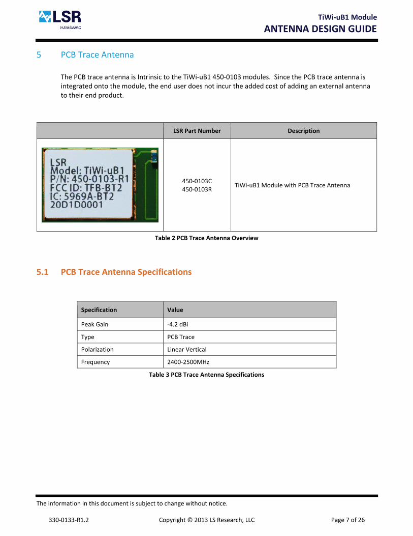
5 PCB Trace Antenna
The PCB trace antenna is Intrinsic to the TiWi-uB1 450-0103 modules. Since the PCB trace antenna is integrated onto the module, the end user does not incur the added cost of adding an external antenna to their end product.
LSR Part Number Description
450-0103C 450-0103R
TiWi-uB1 Module with PCB Trace Antenna
Table 2 PCB Trace Antenna Overview
5.1 PCB Trace Antenna Specifications
Specification Value
Peak Gain -4.2 dBi
Type PCB Trace
Polarization Linear Vertical
Frequency 2400-2500MHz
Table 3 PCB Trace Antenna Specifications

TiWi-uB1 Module
ANTENNA DESIGN GUIDE
The information in this document is subject to change without notice.
330-0133-R1.2 Copyright © 2013 LS Research, LLC Page 8 of 26
6 Dipole Antenna
The LSR 001-0001 Dipole Antenna is used in conjunction with the LSR 080-0001 U.FL to Reverse Polarity SMA Cable, and the Hirose PCB mounted U.FL connector, to provide an externally mounted antenna solution for the TiWi-uB1 450-0106 module.
Part Number Description
450-0106C 450-0106R
TiWi-uB1 Module, RF Castellation
LS Research
001-0001
2.4 GHz Dipole Antenna with Reverse Polarity SMA Connector
LS Research 080-0001
U.FL to Reverse Polarity SMA Bulkhead Cable 105 mm
Hirose U.FL-R-SMT(10)
PCB Mounted U.FL Connector
Table 4 Dipole Antenna Overview

TiWi-uB1 Module
ANTENNA DESIGN GUIDE
The information in this document is subject to change without notice.
330-0133-R1.2 Copyright © 2013 LS Research, LLC Page 9 of 26
6.1 Dipole Antenna Specifications
Specification Value
Gain +2 dBi
Impedance 50 ohms, Nominal
Type Dipole
Polarization Linear Vertical
VSWR ≤2.5:1, Maximum
Frequency 2400-2500MHz
Weight 13g
Size 105×10 mm
Antenna Color Black
Table 5 Dipole Antenna Specifications

TiWi-uB1 Module
ANTENNA DESIGN GUIDE
The information in this document is subject to change without notice.
330-0133-R1.2 Copyright © 2013 LS Research, LLC Page 10 of 26
6.2 Mechanical Dimensions
Figure 1 Dipole Antenna Dimensions

TiWi-uB1 Module
ANTENNA DESIGN GUIDE
The information in this document is subject to change without notice.
330-0133-R1.2 Copyright © 2013 LS Research, LLC Page 11 of 26
7 PCB Layout Requirements
Since this module and its associated set of approved antennas has been certified by the FCC and Industry Canada (IC) as a Modular Radio, the end user is authorized to integrate this module into an end-product, and is solely responsible for the Unintentional Emissions levels produced by the end-product.
In order to preserve the Modular Radio certifications, the integrator of the module must abide by the PCB layout recommendations outlined in the following paragraphs. Any divergence from these recommendations will invalidate the modular radio certifications and require the integrator to re-certify the module and/or end-product.
The module must be used with one of the approved antennas:
1. On module PCB trace antenna.
2. LS Research 001-0001 center-fed 2.4 GHz dipole antenna and 080-0001 U.FL to Reverse Polarity SMA connector cable.
PCB Trace Antenna Implementation When using the PCB Trace Antenna version of the module (Part Number 450-0103), the PCB layout can be removed entirely, as the RF signal does not come out of the module. It is acceptable to keep the U.FL circuitry, and the components J3, C13, C14, and R7 can either be populated or not. 2.4 GHz Dipole Antenna Implementation When using the RF castellation version of the module (Part Number 450-0106), and the certified 2.4 GHz Dipole Antenna and U.FL to RPSMA Cable, the PCB layout shown in Section 7.1 should be followed. Components J3 and R7 should be populated as shown in the schematic in Section 7.2.

TiWi-uB1 Module
ANTENNA DESIGN GUIDE
The information in this document is subject to change without notice.
330-0133-R1.2 Copyright © 2013 LS Research, LLC Page 12 of 26
7.1 Reference Design PCB
Figure 2 Reference Design PCB

TiWi-uB1 Module
ANTENNA DESIGN GUIDE
The information in this document is subject to change without notice.
330-0133-R1.2 Copyright © 2013 LS Research, LLC Page 13 of 26
7.2 Reference Design Schematic
Figure 3 Reference Design Schematic

TiWi-uB1 Module
ANTENNA DESIGN GUIDE
The information in this document is subject to change without notice. 330-0133-R1.2 Copyright © 2013 LS Research, LLC Page 14 of 26
7.3 Reference Design BOM
Qty PCB Ref Pop Option Value Tolerance Manufacturer Mfg Part Number
1 B1 Memory Protection Devices BU2032SM-G
1 C1 NP 100nF +/- 10% Murata GRM155R71C104KA88#
2 C13 C14 NP LSR 000-0000
1 C16 NP 2.4pF +/- 0.1pF Johanson Technology 250R05L2R4BV4T
1 C2 100pF +/- 5% Murata GRM1555C1H101JA01#
2 C3 C6 100nF +/- 10% Murata GRM155R71C104KA88#
2 C5 C7 12pF +/- 5% Murata GRM1555C1H120JA01#
4 C8 C9 C11 C15 2.2uF +/- 20% Kemet C0402C225M9PAC#
2 FB1 FB2 Murata BLM15HG102SN1#
2 J1 J2 Samtec SFM-110-02-L-D-A
1 J3 Hirose U.FL-R-SMT-1#
2 J4 J5 Sullins NRPN121PAEN-RC
1 J6 AMP 640456-2
1 J8 Sullins GRPB052VWQS-RC
1 J9 NP Sullins PRPN021PAEN-RC
3 JMP1 JMP2 JMP3 Sullins SPN02SXCN-RC
3 JP1 JP2 JP3 Sullins NRPN031PAEN-RC
1 L1 2.2uH +/- 30% Murata LQM21PN2R2NGC#
2 L2 L4 5.6nH +/- 0.3nH Johanson Technology L-07C5N6SV6T
1 LED1 Kingbright APTB1612ESGC-F01
1 MOD1 Gigatek 450-0106C
1 PCB1 LSR 750-00490
1 Q4 Fairchild FDN340P
2 R1 R3 10K 5% KOA RK73B1ET#103J
2 R2 R9 270 1% Vishay CRCW0402270RFK#
2 R5 R10 2.7K 1% Vishay CRCW04022K70FK#
1 R7 0 50m Ohm Max KOA RK73Z1ET#
1 R8 NP 10K 5% KOA RK73B1ET#103J
2 S1 S2 Panasonic EVQ-PNF04M
1 U1 Texas Instruments TPS62730DRY#
1 U2 Texas Instruments TMP100NA#
1 X1 ECS ECS-.327-12.5-34B
Notes: # designates mfg material package option.
NP designates a component that is not populated.

TiWi-uB1 Module
ANTENNA DESIGN GUIDE
The information in this document is subject to change without notice. 330-0133-R1.2 Copyright © 2013 LS Research, LLC Page 15 of 26
Table 6 Reference Design EM Board BOM
TiWi-uB1 Module
ANTENNA DESIGN GUIDE
The information in this document is subject to change without notice.
330-0133-R1.2 Copyright © 2013 LS Research, LLC Page 16 of 26
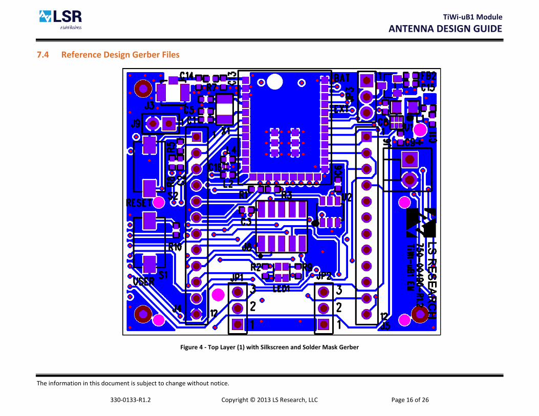
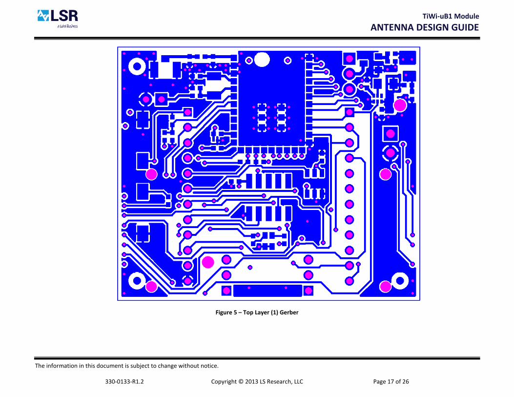
7.4 Reference Design Gerber Files
Figure 4 - Top Layer (1) with Silkscreen and Solder Mask Gerber
TiWi-uB1 Module
ANTENNA DESIGN GUIDE
The information in this document is subject to change without notice.
330-0133-R1.2 Copyright © 2013 LS Research, LLC Page 17 of 26
Figure 5 – Top Layer (1) Gerber

TiWi-uB1 Module
ANTENNA DESIGN GUIDE
The information in this document is subject to change without notice.
330-0133-R1.2 Copyright © 2013 LS Research, LLC Page 18 of 26
Figure 6 - Layer 2 Gerber

TiWi-uB1 Module
ANTENNA DESIGN GUIDE
The information in this document is subject to change without notice.
330-0133-R1.2 Copyright © 2013 LS Research, LLC Page 19 of 26
Figure 7 - Layer 3 Gerber

TiWi-uB1 Module
ANTENNA DESIGN GUIDE
The information in this document is subject to change without notice.
330-0133-R1.2 Copyright © 2013 LS Research, LLC Page 20 of 26
Figure 8 – Bottom Layer (4) Gerber

TiWi-uB1 Module
ANTENNA DESIGN GUIDE
The information in this document is subject to change without notice.
330-0133-R1.2 Copyright © 2013 LS Research, LLC Page 21 of 26
Figure 9 – Bottom Layer (4) with Silkscreen and Solder Mask Gerber

TiWi-uB1 Module
ANTENNA DESIGN GUIDE
The information in this document is subject to change without notice.
330-0133-R1.2 Copyright © 2013 LS Research, LLC Page 22 of 26
7.5 Reference Design - U.FL RF Trace Dimensions
Figure 10 – U.FL RF Trace Details

TiWi-uB1 Module
ANTENNA DESIGN GUIDE
The information in this document is subject to change without notice. 330-0133-R1.2 Copyright © 2013 LS Research, LLC Page 23 of 26
7.6 U.FL Connector Drawing
Figure 11 – U.FL Connector Drawing

TiWi-uB1 Module
ANTENNA DESIGN GUIDE
The information in this document is subject to change without notice.
330-0133-R1.2 Copyright © 2013 LS Research, LLC Page 24 of 26
8 EMC Compliance
8.1 Summary
The TiWi-uB1 module has been tested and approved as a Modular Radio in accordance with the appropriate FCC and IC standards. The supporting test data may be found in the modular test report.
Since this module and its associated set of approved antennas have been certified as a Modular Radio, this allows the end user to integrate this module into an end-product without the requirement of re-certifying the radio module. The module-integrator is responsible for the unintentional conducted and radiated emissions and must verify that the integrated product is compliant with the rules associated with unintentional radiators. The module integrator is also required to maintain an engineering record of the verification testing and declare on the product through proper labeling and marking that the device is compliant with these particular rules. The module integrator is responsible for using the patch file that corresponds to the antenna configuration and region for EMC compliance.
The installed module’s FCC ID and IC numbers need to be clearly marked on the product with the following verbiage “Contains FCC ID: TFB-BT2” and "Contains IC: 5969A-BT2".
The TiWi-uB1 has been certified for use in a portable configuration, which allows a transmitting device to be used with any part of its radiating structure in direct contact with the user’s body or within 20 cm of the body of a user or bystanders under normal operating conditions.
8.2 Module Integration Considerations - Antenna Systems
The module must be used with one of the approved antennas:
1. On module PCB trace antenna.
2. LS Research 001-0001 center-fed 2.4 GHz dipole antenna and LS Research 080-0001 U.FL to Reverse Polarity SMA connector cable.
The antenna should be placed such that it is minimally disturbed by the product’s packaging material. The incorporation of the largest practical free-space clearance around the antenna is important for maximizing overall performance. Further, the antenna must be placed such that at least a 20 cm separation distance is maintained from the antenna to all other radio transmitters.
8.3 Module Integration Considerations - Substitute Antenna Systems
The module’s certification is only valid for the list of approved antennas presented in section 4. However, substitute antennas may be used in place of the approved antenna only if the antennas are of the same type and the peak gain is less than or equal to the peak gain of the similar approved antenna. Also the antennas should have similar in-band and out-of-band characteristics.
8.4 Module Integration Considerations - Circuit Implementation
It is recommended that all connection PCB (printed circuit board) traces to the power supply and digital control terminal be as short as possible. Though not necessarily required in all cases, it is

TiWi-uB1 Module
ANTENNA DESIGN GUIDE
The information in this document is subject to change without notice.
330-0133-R1.2 Copyright © 2013 LS Research, LLC Page 25 of 26
a best practice to provide an optional shunt capacitor placement at the module pin on all active and routed power supply and digital control lines. Further, a series damping resistor placement should be incorporated between the module pin/shunt capacitor node and the source/sink of the digital control signals. This provides for effective bypassing and decoupling of digital lines from the radio module, in the event that the application circuit has longer power supply and digital routing.
8.5 Module Integration Considerations - Top Assembly
In addition to the recommendations given for the antenna systems and the module placement onto a product PCB, it is recommended that all wiring and interconnect systems within the product be not routed anywhere close the module and its associated circuitry on the PCB, doing so could change the emission characteristics of the module.
8.6 Testing Requirements for End-Product
Once the module is integrated and the product realized in a mobile or portable configuration, the product must be tested and follow the verification process for Unintentional Conducted and Radiated Emissions in accordance to the FCC and IC guidelines. The module needs to be powered and placed in the receive mode for this test. The receiver must be tuned to its lowest frequency channel, mid-frequency channel, and highest frequency channel. The supporting test data does not need to be submitted to the FCC or IC.
8.7 SAR Testing Requirements for End-Product
Since the TiWi-uB1 radio module was certified in a portable configuration, the end-product does not require SAR testing assuming it is not located within 20 cm of another transmitter.

TiWi-uB1 Module
ANTENNA DESIGN GUIDE
The information in this document is subject to change without notice.
330-0133-R1.2 Copyright © 2013 LS Research, LLC Page 26 of 26
9 Contacting LS Research
Headquarters LS Research, LLC W66 N220 Commerce Court Cedarburg, WI 53012-2636 USA Tel: 1(262) 375-4400 Fax: 1(262) 375-4248
Website www.lsr.com
Wiki www.lsr.com/products-wiki
Technical Support www.lsr.com/products-forum
Sales Contact [email protected]
The information in this document is provided in connection with LS Research (hereafter referred to as “LSR”) products. No license, express or implied, by estoppel or otherwise, to any intellectual property right is granted by this document or in connection with the sale of LSR products. EXCEPT AS SET FORTH IN LSR’S TERMS AND CONDITIONS OF SALE LOCATED ON LSR’S WEB SITE, LSR ASSUMES NO LIABILITY WHATSOEVER AND DISCLAIMS ANY EXPRESS, IMPLIED OR STATUTORY WARRANTY RELATING TO ITS PRODUCTS INCLUDING, BUT NOT LIMITED TO, THE IMPLIED WARRANTY OF MERCHANTABILITY, FITNESS FOR A PARTICULAR PURPOSE, OR NON-INFRINGEMENT. IN NO EVENT SHALL LSR BE LIABLE FOR ANY DIRECT, INDIRECT, CONSEQUENTIAL, PUNITIVE, SPECIAL OR INCIDENTAL DAMAGES (INCLUDING, WITHOUT LIMITATION, DAMAGES FOR LOSS OF PROFITS, BUSINESS INTERRUPTION, OR LOSS OF INFORMATION) ARISING OUT OF THE USE OR INABILITY TO USE THIS DOCUMENT, EVEN IF LSR HAS BEEN ADVISED OF THE POSSIBILITY OF SUCH DAMAGES. LSR makes no representations or warranties with respect to the accuracy or completeness of the contents of this document and reserves the right to make changes to specifications and product descriptions at any time without notice. LSR does not make any commitment to update the information contained herein. Unless specifically provided otherwise, LSR products are not suitable for, and shall not be used in, automotive applications. LSR’s products are not intended, authorized, or warranted for use as components in applications intended to support or sustain life.