answer optical technology assignment
TRANSCRIPT

8/8/2019 Answer Optical Technology Assignment
http://slidepdf.com/reader/full/answer-optical-technology-assignment 1/25
2010
Amity Institute Of InformationTechnology
Saket Kumar Pathak M.Sc. NT & M
Optical Technology An introductory detail of the topics – subtopics defined as well as designed throughout thesyllabus with possible explanatory diagrams and pictorial representation.

8/8/2019 Answer Optical Technology Assignment
http://slidepdf.com/reader/full/answer-optical-technology-assignment 2/25
Optical Fiber Communication
Q. No. 1. Difference Between LEDs and Lasers
LEDs Lasers
LEDs are semiconductor diode that
converts applied voltage to light and is used
in lamps and digital displays.
Laser diode is formed from a p-n junctionand powered by injected electric current.
LEDs are made from compoundsemiconductor materials such as galliumarsenide (GaAs), gallium phosphide (GaP),gallium arsenide-phosphide (GaAsP).
The former devices are sometimes referredto as Injection Laser Diodes
A LED is basically just a specialized type of
P-N junction diode, made from a thin chipof fairly heavily doped semiconductormaterial.
Laser diodes form a subset of the largerclassification of semiconductor p-n junction diodes.
The color of the light emitted, inthe case is visible light.
The key parameter for a laser diode is thethreshold current, which is the forwardcurrent level where lasing actually begins tooccur.
LEDs are intended to operate only inforward conduction mode, and should not
be subjected to reverse voltage.
Another important parameter is the ratedlight output, which is the highestrecommended light output level for reliablecontinuous operation.
LEDs light output isn’t coherent, it is
comparatively high in noise and hence notsuitable for use as a carrier for datacommunications.
Laser’s light output is coherent; it is very low in noise and also more suitable for useas a carrier for data communications.
The bandwidth also tends to be widerthan Lasers, making them not suitablefor optical systems.
Although most of the laser diodes used inelectronic equipment are capable of causing damage to a human or animal eye,and particularly to its light-sensitive retina.
An LED is often small in area (less than
1 mm2), and integrated optical components
may be used to shape its radiation pattern.
Infra-red (IR) lasers are especially capableof causing eye damage, because their lightis not visible.
LEDs present many advantages as lower
energy consumption, longer lifetime,smaller size, faster switching, and greater
durability and reliability.
A laser diode is a laser where the activemedium is a semiconductor similar to thatfound in a light-emitting diode.
Light-emitting diodes or LEDs are now very widely used in almost every area of electronics, mainly as indicator and display devices in effect, solid state lamps.
A laser diode is formed by doping a very thin layer on the surface of a crystal wafer.
Amity Institute Of Technology Page 2
8/8/2019 Answer Optical Technology Assignment
http://slidepdf.com/reader/full/answer-optical-technology-assignment 3/25
Optical Fiber Communication
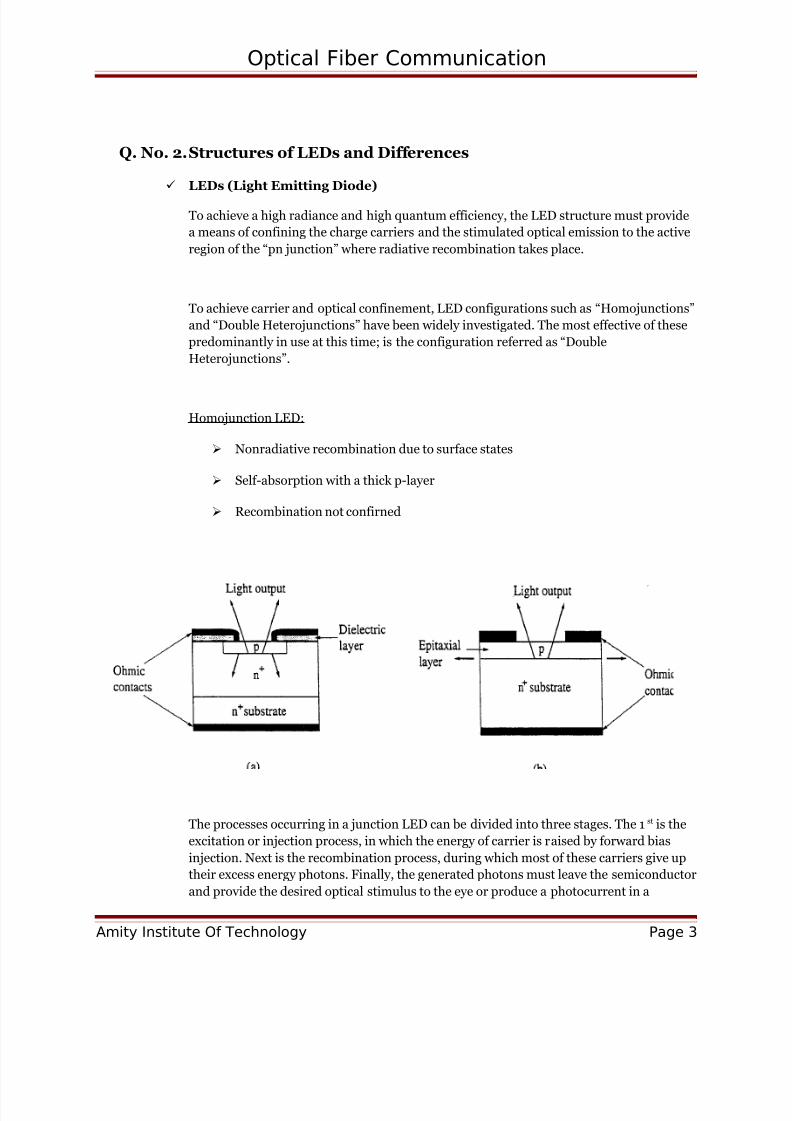
Q. No. 2.Structures of LEDs and Differences
LEDs (Light Emitting Diode)
To achieve a high radiance and high quantum efficiency, the LED structure must provide
a means of confining the charge carriers and the stimulated optical emission to the active
region of the “pn junction” where radiative recombination takes place.
To achieve carrier and optical confinement, LED configurations such as “Homojunctions”
and “Double Heterojunctions” have been widely investigated. The most effective of these
predominantly in use at this time; is the configuration referred as “Double
Heterojunctions”.
Homojunction LED:
Nonradiative recombination due to surface states
Self-absorption with a thick p-layer
Recombination not confirned
The processes occurring in a junction LED can be divided into three stages. The 1st is the
excitation or injection process, in which the energy of carrier is raised by forward bias
injection. Next is the recombination process, during which most of these carriers give up
their excess energy photons. Finally, the generated photons must leave the semiconductor
and provide the desired optical stimulus to the eye or produce a photocurrent in a
Amity Institute Of Technology Page 3

8/8/2019 Answer Optical Technology Assignment
http://slidepdf.com/reader/full/answer-optical-technology-assignment 4/25
Optical Fiber Communication
detector. This is the extraction process. These processes have a characteristics efficiency,
and the over all device efficiency, η(0), may then be expressed as
η (0) = η(in) η(r) η(e)
where;
η(0) is external conversion efficiency,
η(in) is injection,
η(r) is radiative recombination,
η(e) is extraction efficiency.
Double Heterojunctions:
Top n+ -GaAs and bottom p+ -GaAs for ohmic contacts
A well is etched into n+ -GaAs
Back metal contact reflects backward light.
This configuration evolved from earlier studies on laser diodes. By means of this
sandwich structure of differently composed alloy layers, both the carriers and the optical
field are confirmed in the central active layer. The band-gap differences of adjacent layers
confine the charge carriers (fig. b), while the differences in the indices of refraction of
adjoining layer confine the optical field to the central active layer (fig. c). This dully
confinement leads to both high efficiency and high radiance. Other parameter influencing
the device performance includes, optical absorption in the active region (self-absorption),
carrier recombination at the heterostructure interface.
Q. No. 3.Performance of LEDs (Distributed and Fabry-Perote)
Fabry-Perote Resonator:
In laser diode Fabry-Perot resonator, a pair of flat partially reflecting mirrors are directed
toward each other to enclose to cavity. The mirror facets are constructed by making twoparallel cleaves along natural cleavage planes of the semiconductor crystal. The purpose
of these mirrors is to provide strong optical feedback in the longitudinal direction,
thereby converting the device into an oscillator with a gain mechanism that compensates
for optical losses in the cavity. The laser cavity can have many resonant frequencies. The
device will oscillate (by emitting light) at those resonant frequencies for which the gain is
sufficient to overcome the losses. The sides of the cavity are simply formed by roughening
the edge of the device to reduce unwanted emissions in the directions.
Amity Institute Of Technology Page 4

8/8/2019 Answer Optical Technology Assignment
http://slidepdf.com/reader/full/answer-optical-technology-assignment 5/25
Optical Fiber Communication
Fabry-Perote Laser Diode
Distributed Feedback Laser Diode
Distributed Feed-Back:
Another laser diode type, commonly referred to as the distributed-feedback (DFB) laser,
the cleaved facets are not required for optical feedback. The fabrication is obtained from
Bragg reflectors (gratings) or periodic variations of refractive index called distributed-
Feedback corrugations which are incorporated into the multilayer structure along the
length of the diode.
Q. No. 4.Principle of Laser diodes (population inversion)
The term “laser” is an acronym for (L)ight (A)mplification by (S)timulated (E)mission of
(R)adiation. To understand the laser, one needs to understand the meaning of theseterms. The term “light” is generally accepted to be electromagnetic radiation ranging from1 nm to 1000 mm in wavelength. The visible spectrum (what we see) ranges fromapproximately 400 to 700 nm. The wavelength range from 700 nm to 10 mm isconsidered the near infrared (NIR), and anything beyond that is the far infrared (FIR).Conversely, 200 to 400 nm is called ultraviolet (UV); below 200 nm is the deepultraviolet (DUV).
Principles of Laser Diodes:
Amity Institute Of Technology Page 5
8/8/2019 Answer Optical Technology Assignment
http://slidepdf.com/reader/full/answer-optical-technology-assignment 6/25
Optical Fiber Communication
The GaAIAs Laser Diode consists of a double hetero junction formed by a Gal-YAIYAsactive layer surrounded by P-type and N-type Gal-, AlxAs cladding layers, where x y,
when a bias voltage is applied In the forward direction, electrons and holes are Injectedinto the active layer. Since the band gap energy is greater in the cladding layers than in
the active layer, the injected electrons and holes are prevented from diffusing across the junction by the potential barriers formed between the active layer and cladding layers.The electrons and holes confined to the active layer create a state of population Inversion,allowing the amplification of light by stimulated emission. The light amplification gainsacross the hetero action. The high refractive Index of the active layer, as compared to thecladding layers, serves to confine the emitted light to propagation within the active layer.The confinement of the charge carriers and the emitted light are the keys to highly efficient laser diodes.
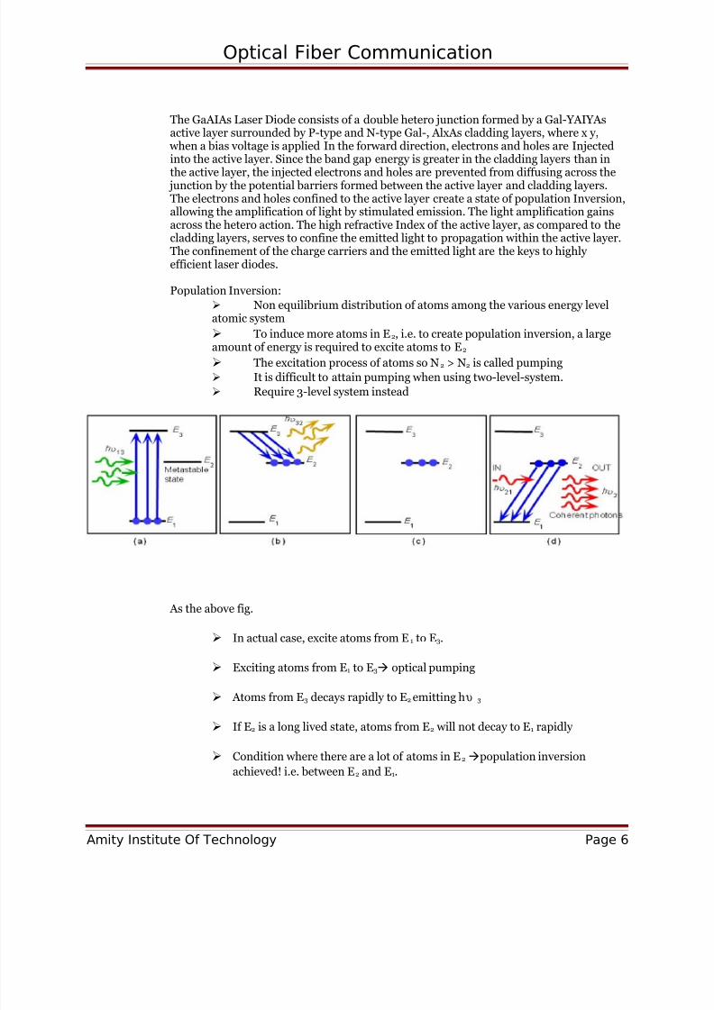
Population Inversion:
Non equilibrium distribution of atoms among the various energy levelatomic system
To induce more atoms in E2, i.e. to create population inversion, a largeamount of energy is required to excite atoms to E2
The excitation process of atoms so N2 > N2 is called pumping
It is difficult to attain pumping when using two-level-system.
Require 3-level system instead
As the above fig.
In actual case, excite atoms from E1 to E3.
Exciting atoms from E1 to E3à optical pumping
Atoms from E3 decays rapidly to E2 emitting hυ 3
If E2 is a long lived state, atoms from E2 will not decay to E1 rapidly
Condition where there are a lot of atoms in E2 àpopulation inversion
achieved! i.e. between E2 and E1.
Amity Institute Of Technology Page 6

8/8/2019 Answer Optical Technology Assignment
http://slidepdf.com/reader/full/answer-optical-technology-assignment 7/25
Optical Fiber Communication
Q. No. 5.Power Launching and Coupling
Launching optical power from a source into a fiber entails considerations such as
numerical aperture, core size, refractive-index profile, and core cladding index difference
of the fiber, plus the size, radiance, and angular power distribution of the optical source.
A measure of the amount of optical power emitted from a source that can be coupled into
a fiber is usually given by the efficiency η defined as:
η =P(F)/P(S)
Here, P(F) is power coupled into fiber and P(S) is the power emitted from the light
source. The launching and coupling efficiency depends on the type of fiber that is
attached to the source and on the coupling process.
In practice, manysource suppliers offer deviceswith a short length optical fiber (1m or
less) already attached in a optimum power coupling configuration. This section of fiber is
generally referred as “Flylead” or “Pigtail”. The effect to be considered in this case
include:
• Types of fiber attached to source.
• Coupling process.
• Fiber misalignment.
• Different core-size.
• Numerical aperture.
• Core refractive-index profile.
In case of numerical aperture difference with the source beam profile,
B(θ) = Bo Cosθ
Where, θ = Direction away from the axis,
Bo = Intensity on the axis.
The power coupled into a step index fiber,
Pf = Ps (NA)² ;if r<a
(a/r)² Ps (NA)² ; if r>a
Amity Institute Of Technology Page 7
8/8/2019 Answer Optical Technology Assignment
http://slidepdf.com/reader/full/answer-optical-technology-assignment 8/25
Optical Fiber Communication
Where, r and a are the source and fiber radial dimensions.
When the size of the source is smaller than that of the fiber and is in close contact with
the fiber and the coupling efficiency becomes,
η =P(F)/P(S) = (NA)²
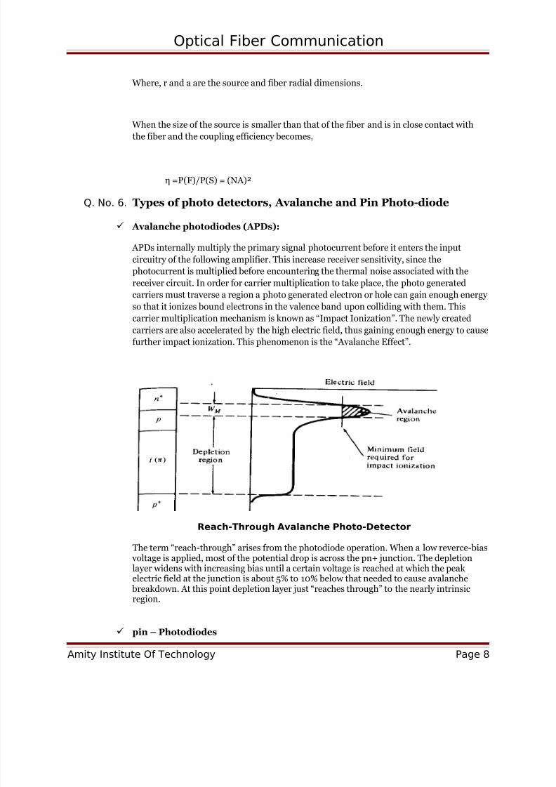
Q. No. 6. Types of photo detectors, Avalanche and Pin Photo-diode
Avalanche photodiodes (APDs):
APDs internally multiply the primary signal photocurrent before it enters the input
circuitry of the following amplifier. This increase receiver sensitivity, since the
photocurrent is multiplied before encountering the thermal noise associated with thereceiver circuit. In order for carrier multiplication to take place, the photo generated
carriers must traverse a region a photo generated electron or hole can gain enough energy
so that it ionizes bound electrons in the valence band upon colliding with them. This
carrier multiplication mechanism is known as “Impact Ionization”. The newly created
carriers are also accelerated by the high electric field, thus gaining enough energy to cause
further impact ionization. This phenomenon is the “Avalanche Effect”.
Reach-Through Avalanche Photo-Detector
The term “reach-through” arises from the photodiode operation. When a low reverce-bias voltage is applied, most of the potential drop is across the pn+ junction. The depletionlayer widens with increasing bias until a certain voltage is reached at which the peak electric field at the junction is about 5% to 10% below that needed to cause avalanche
breakdown. At this point depletion layer just “reaches through” to the nearly intrinsicregion.
pin – Photodiodes
Amity Institute Of Technology Page 8

8/8/2019 Answer Optical Technology Assignment
http://slidepdf.com/reader/full/answer-optical-technology-assignment 9/25
Optical Fiber Communication
The most common semiconductor photo detector is the pin photodiode. The device
structure consists of p and n regions separated by a very lightly n-doped intrinsic (i)
region. In normal operation a sufficiently large reverse-bias voltage is applied across the
device so that the intrinsic region is fully depleted of carriers. That is, the intrinsic n and p
carrier concentration are negligibly small in comparison with the impurity concentration
in this region.
When an incident photon has energy greater than or equal to the band-gap energy of the
semiconductor material, the photon can give up its energy and excite an electron from the
valence band to the conduction band. This process generates photon-carriers. The photo
detector is normally designed so that these carriers are generated mainly in the depletion
region where most of the incident light is absorbed. The high electric field present in the
depletion region causes the carriers to separate and be collected across the reverse-bias
junction. This gives rise to a current flow in an external circuit, with one electron flowing
for every carrier pair generated. This current flow is known as the photocurrent.
Q. No. 7. Optical Receiver (Design and Diagram)
The main component of an optical receiver is a photo detector, which convertslight into electricity using the photoelectric effect. The photo detector is typically
a semiconductor-based photodiode. Several types of photodiodes include p-n
photodiodes, a p-i-n photodiodes, and avalanche photodiodes. Metal-semiconductor-metal (MSM) photo detectors are also used due to their suitability
for circuit integration in regenerators and wavelength-division multiplexers.
Basic Optical Receiver Front-End
Amity Institute Of Technology Page 9

8/8/2019 Answer Optical Technology Assignment
http://slidepdf.com/reader/full/answer-optical-technology-assignment 10/25
Optical Fiber Communication
Requirements
General:
Low-noise electronics for optical to electrical signal conversion
Short to medium haul application
2+ Gbps data rate
Input side:
InGaAs Photodiode with junction capacitance ~ 100 ff’s
Optical powers ranging from -20 to +10 dBm, causing input currents from 10uA to 10mA
Output side:
Drive a capacitive load representing subsequent MOSFET gate
Digital signal RZ-type output
Photo detection is the process of conversion from optical to electrical domain. A block
diagram of the GMRT optical receiver is shown in following fig.. The basic detector is a
reverse biased p-n junction diode. In this bias condition a reverse leakage current (thedark current ) flows. The other important characteristic of a photo-detector is its
responsively . The responsively is a measure of the efficiency with which light is
converted to electrical current and it is related to the width of the depletion region of the
diode and to the spectral response of the receiver. A larger depletion region leads to a
better responsively. PIN diode detectors made of InGaAsP and grown on InP are popular
photo-detectors as they have low dark currents and high responsively.
Amity Institute Of Technology Page 10
8/8/2019 Answer Optical Technology Assignment
http://slidepdf.com/reader/full/answer-optical-technology-assignment 11/25
Optical Fiber Communication
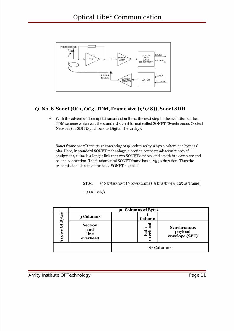
Q. No. 8.Sonet (OC1, OC3, TDM, Frame size (9*9*8)), Sonet SDH
With the advent of fiber optic transmission lines, the next step in the evolution of the
TDM scheme which was the standard signal format called SONET (Synchronous Optical
Network) or SDH (Synchronous Digital Hierarchy).
Sonet frame are 2D structure consisting of 90 columns by 9 bytes, where one byte is 8
bits. Here, in standard SONET technology, a section connects adjacent pieces of
equipment, a line is a longer link that two SONET devices, and a path is a complete end-
to-end connection. The fundamental SONET frame has a 125 µs duration. Thus the
transmission bit rate of the basic SONET signal is;
STS-1 = (90 bytes/row) (9 rows/frame) (8 bits/byte)/(125 µs/frame)
= 51.84 Mb/s
90 Columns of Bytes
9 r o w s O f B y t e s
3 Columns1
Column
Sectionandline
overhead P a t h
o v e r h
e a d
Synchronous
payloadenvelope (SPE)
87 Columns
Amity Institute Of Technology Page 11

8/8/2019 Answer Optical Technology Assignment
http://slidepdf.com/reader/full/answer-optical-technology-assignment 12/25
Optical Fiber Communication
This is called an STS-1 signal, where STS stands for synchronous transport signal. All
other SONET signals are integer multiples of this rate, so that STS-N signal modulate an
optical source, the logical STS-N signal is first scrambled to avoid long string of ones and
zeros and to allow easier clock recovery at the receiver. After under going electrical-to-
optical conversion the resultant physical layer optical-signal is called OC-N, where OC
stands for Optical carrier.
In SDH the basic rate is equivalent to STS-3 or 155.52 mb/s, this is called “Synchronous
transport module – level-1”. Higher rates are designated by STS-M. Values of M
supported by IUT-T as, M = 1, 4, 16, 64. These are equivalent to SONET OC-N signals,
where N = 3M. Analogous to SONET, SDH first scrambles the logical signal. In contrast
to SONET, SDH doesn’t distinguish between a logical electrical signal and a physical
optical signal, so that both signal types are designated by STM-M. Following we have a
list of commonly used values.
SONET level Electrical level Line rate (Mb/s) SDH equivalent
OC-1 STS-1 51.84 -
OC-3 STS-3 155.52 STM-1
OC-12 STS-12 622.08 STM-4
OC-24 STS-24 1244.16 STM-8
OC-48 STS-48 2488.32 STM-16
OC-96 STS-96 4976.64 STM-32
OC-192 STS-192 9953.28 STM-64
Optical Interfaces:
The SONET/SDH specifications provide details for the optical source characteristics, the
receiver sensitivity and transmission distances for various types of fibers. 6 Transmission
ranges are defined as following, with different terminology for SONET/SDH.
Transmission Distance SONET Technology SDH Terminology
≤ 2 km Short – reach Intra-office
15 km Intermediate reach Short – Haul
40 km at 1310 nm Long – reach Long Haul
80 km at 1550 nm
120 km at 1550 nm Very Long – Haul
Amity Institute Of Technology Page 12

8/8/2019 Answer Optical Technology Assignment
http://slidepdf.com/reader/full/answer-optical-technology-assignment 13/25
Optical Fiber Communication
160 km at 1550 nm Ultra long – Haul
The optical fiber generally fall into the following 3 categories and operation windows:
1. Graded – Index multimode in the 1310-nm window.
2. Conventional non-dispersion-shifted single-mode in 1310 nm and 1550 nm
window.
3. Dispersion-Shifted single – mode in the 1550 nm window.
SONET/SDH Networks:
An important SONET/SDH network element is the add/drop multiplexer (ADM). This
piece of equipment is a fully synchronous, byte-oriented multiplexer that is used to add
and drop sub channels within an OC-N signals.
As in the following figure, various OC-12 and OC-3 are multiplexed into an OC-48 stream.
Upon entering an ADM, these sub-channels can be individually dropped by the ADM and
others can be added. One OC-12 and two OC-3 channels enter the left-most ADM as part
of an OC-48 channel. The OC-12 is passed through and two OC-3 are dropped by the first
ADM. Then, two more OC-12 and one OC-3 are multiplexed together with the OC-12
channel that is passing through and the aggregate OC-48 is sent to another ADM node
downstream.
Q. No. 9. WDM, Types of coupling, Operational Principle, 2x2 coupler
(Splitting Ration), Start Coupler, Mach-Zehnder Interferometer
Multiplexers.
Amity Institute Of Technology Page 13

8/8/2019 Answer Optical Technology Assignment
http://slidepdf.com/reader/full/answer-optical-technology-assignment 14/25
Optical Fiber Communication
The technology of combining a number of wavelengths onto the same fiber is known as
“Wave-Length Division Multiplexing” or WDM. Conceptually, the WDM scheme is the
same as FDM used in microwave radio and satellite systems. The key system features of
WDM are as follows:
o Capacity Upgrade: - The classical application of WDM has been to upgrade the
capacity of existing point-to-point fiber optic transmission links that can increase
the capacity of fiber network dramatically.
o Transparency: - An important aspect of WDM is that, each optical channel can
carry any transmission format. Thus, by using different wavelengths, fast or slow
asynchronous or synchronous digital data and analog information can be sent
simultaneously and independently, over the same fiber channel.
o Wavelength routing: - wavelength sensitive optical routing devices using
multiple wavelengths to increase link capacity and flexibility, and treats
wavelength as another dimension in addition to time and space. Wavelength
routed networks use the actual wavelength of a signal as the intermediate or final
address.
o Wavelength Switching: - Wavelength routed networks are based on a rigid
fiber infrastructure, wavelength-switched architectures allow reconfigurations of
optical layers. Key components for implementing these networks include optical
add/drop multiplexer, optical cross connects and add/drop multiplexers.
Operational Principle
In standard point-to-point links a single fiber line has one optical source at itstransmitting end and one photo detector at the receiving end. Signal from different light
sources use separate and uniquely assigned optical fiber. Since an optical source has
narrow line width, these types of transmission make use of narrow portion of the
transmission bandwidth capacity of a fiber.
Amity Institute Of Technology Page 14
8/8/2019 Answer Optical Technology Assignment
http://slidepdf.com/reader/full/answer-optical-technology-assignment 15/25
Optical Fiber Communication
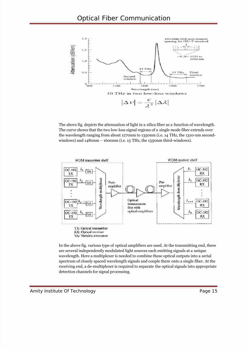
The above fig. depicts the attenuation of light in a silica fiber as a function of wavelength.
The curve shows that the two low-loss signal regions of a single mode fiber extends over
the wavelength ranging from about 1270nm to 1350nm (i.e. 14 THz, the 1310-nm second-
windows) and 1480nm – 1600nm (i.e. 15 THz, the 1550nm third-windows).
In the above fig. various type of optical amplifiers are used. At the transmitting end, thereare several independently modulated light sources each emitting signals at a unique
wavelength. Here a multiplexer is needed to combine these optical outputs into a serial
spectrum of closely spaced wavelength signals and couple them onto a single fiber. At the
receiving end, a de-multiplexer is required to separate the optical signals into appropriate
detection channels for signal processing.
Amity Institute Of Technology Page 15

8/8/2019 Answer Optical Technology Assignment
http://slidepdf.com/reader/full/answer-optical-technology-assignment 16/25
Optical Fiber Communication
The 2X2 fiber couplers
On discussing couplers and splitters, it is to refer in terms of the number of input and
output ports on the device. Hence a device with 2 inputs and 2 outputs would be called as
“2X2 coupler”, similarly N*M coupler has N inputs and M outputs.
In following fig. a common construction is the fused fiber coupler. This is fabricated by
twisting together, melting and pulling two single mode fibers so they get fused together
over a uniform section of length ‘W’. Each input and output fiber has a long tapered
section of length ‘L’, since the transverse dimensions are gradually reduced down to that
of coupling region when the fibers are pulled to fusion process. The total draw length is
L+W. This device is known as fused bi-conical tapered coupler. Here P0 is the input
power, P1 is the throughput power and P2 is the power coupled into the second fiber. The
parameter P3 and P4 are extremely low signal level resulting from backward reflections
and scattering due to bending in and packaging of the device.
Splitting Ratio: To specify the performance of optical coupler one usually indicates the
percentage division of optical power between the output ports by means of ‘splitting
ratio’.
i.e. Splitting Ratio = (P2 / (P1 + P2)) * 100%
Excess Loss: It is defined as the ratio of input power to the total output power.
i.e. Excess Loss = 10 log (P0 / (P1 + P2))
Insertion Loss: It refers to the loss for a particular port-to-port path. If the path of
input has port ‘Pi’ to the path of output has port ‘Pj’, then
Amity Institute Of Technology Page 16

8/8/2019 Answer Optical Technology Assignment
http://slidepdf.com/reader/full/answer-optical-technology-assignment 17/25
Optical Fiber Communication
Insertion Loss = 10 log (Pi / Pj)
Crosstalk: It measures the degree of isolation between the input at one port and the
optical power scattered or reflected back into other the other input port. Hence theoptical power level P3 as;
Crosstalk = 10 log (P3 / P0)
Star Coupler:
The principle role of star coupler is to combine the powers from N inputs and divide them
equally among M output ports. The fiber-fusion technique has been a popular
construction method for N X N star couplers. Following fig. shows, 8 X 8 device formed
by using 12, 2 X 2 couplers. This device could be made from either fused fiber or
integrated optic components. Similarly as to construct 16 X 16 coupler we need 24, 2 X 2interconnected couplers.
Mach-Zehnder Interferometer Multiplexers:
Wavelength-dependent multiplexers can also be made using Mach-Zehnder
interferometer technique. These devices either passive or active. As the following fig. of
passive 2 X 2 MZI consists of three stages: an initial 3Db directional coupler which splitsthe input signals, a central signal where one of the waveguides is longer by ∆L to give a
wavelength dependent phase shift between the two arms, and another 3Db coupler, which
recombines the signal at the output. The function of this arrangement is that, by splitting
the input beam and introducing a phase shift in one of the paths, the recombined signals
with interfere constructively at one output and destructively at the other. The signals then
finally emerge from only one output port.
Amity Institute Of Technology Page 17

8/8/2019 Answer Optical Technology Assignment
http://slidepdf.com/reader/full/answer-optical-technology-assignment 18/25
Optical Fiber Communication
Q. No. 10. Optical Attenuators, Optical Power meter and OTDR
Optical Attenuators:
Whenever a high optical signal level may need to be measured and the level is so high
such that an strong output coming from the amplifier needs to be precisely attenuated
before being measured. This is done to prevent instrument damage and to avoid overload
distortion in measurements.
Optical attenuators allow a user to reduce an optical signal level up to 60 dB in presice
steps at a specified wavelength, which is usually 1310 nm or 1550 nm.
Optical Power meter:
Optical power measurement is the most basic function in fiber optic metrology. Hand-held instruments come in wide variety of types in different levels of capabilities. Multi
wavelength optical power meters that use photo-detectors are the most common
instrument for measuring optical signal power level.
In this versatile instrument various photo-detector heads that have different performance
characteristics are available. As example, GE detector allows a measuring range of + 18
dBm to -60 dBm in 780 nm to 1600 nm wavelength band whereas an InGaAs detector
allows a measuring range of + 3dBm to – 73 dBm in 840 nm to 1650 nm wavelength
band.
Optical Time-Domain Reflectometer (OTDR):
The long term workshop instrument in fiber optic system is the OTDR. In addition to
locating faults, within an optical link, these instrument measures parameter such as
attenuation, length, connector, splice losses and reflectance level. A typical OTDR
consists of optical source and receiver, a data acquisition module, a CPU, an information
Amity Institute Of Technology Page 18

8/8/2019 Answer Optical Technology Assignment
http://slidepdf.com/reader/full/answer-optical-technology-assignment 19/25
Optical Fiber Communication
storage unit for retaining data either in the internal memory or on an external disk and a
display.
An OTDR is fundamentally optical radar. It operates by periodically launching narrow
laser pulses into one end of fiber under test by using either a directional coupler or a
beam splitter. The properties of optical fiber link are then determined by analyzing theamplitude and temporal characteristics of waveform of the back scattering light.
Q. No. 11. Fiber to Fiber joints and types, Fiber end Face
Preparation, Fiber-Related Losses
Significant factor in any fiber optic system installation is the requirement to interconnect
fibers in low – loss manner. A particular technique selected for joining fibers depends on
whether a permanent bond or easily demounted connection is desired. A permanent bond
is generally referred as to as a splice, whereas the demounted joint is known as a
connector. These connections occurs at the following cases of interconnection:
o At the optical source.
o At the photo-detector.
o At the intermediate point within a cable, where two fibers are joined.
o At intermediate point within a link, where two cables are connected.
Every joining technique is subject to a certain conditions which can cause various amount
of optical power loss at the joint. The parameters of these losses are:
o Input power distribution to joint.
o Length of fiber between optical source and joints.
o The geometric and waveguide characteristics of two fiber end at the joints.
o The fiber end faces quality.
Mechanical alignment is a major problem when joining two fibers, owing to their
microscopic size. Radiation losses results from mechanical misalignment, because the
radiation cone of the emitting fiber doesn’t match the acceptance cone of the receiving
Amity Institute Of Technology Page 19

8/8/2019 Answer Optical Technology Assignment
http://slidepdf.com/reader/full/answer-optical-technology-assignment 20/25
Optical Fiber Communication
fiber. The magnitude of the radiation loss depends on the degree of misalignment. The
three fundamental type of misalignment between fiber are:
o Longitudinal separation, when the fibers have same axis and the gaps
between them.
o Angular Alignment, when the two axis forms an angle so that the fiber end
faces are no longer parallel.
o Axial displacement, when the axis of two fibers is separated by a distance. This
is also known as lateral displacement.
Fiber End-Face Preparation:
Before fibers are connected or spliced to each-other, it is necessary to prepare fiber end
faces properly. In order not to have light deflected or scattered at the joint the fiber end
must be flat, perpendicular to fiber axis and smooth. This end-face preparation technique
that have been extensively used, include:
o Sawing
o Gridding and Polishing
o Controlled fracture.
Conventional Gridding and Polishing techniques can produce a very smooth surface that
is perpendicular to the fiber axis. This procedure employed is to use successively finer
abrasives to polish the fiber. Each successive abrasive polish the end face of the fiber,
until the scratches created by previous abrasive material are replaced by finer scratches of
present abrasive. The number of abrasive used depends on the degree of smoothness thatis desired.
Controlled fracture techniques are based on score-and-break methods for cleaving fibers.
As in the following fig. in this operation, the fiber to be cleaved is first scattered to create
stress concentration at the surface. The fiber is then bent over the curve form, while
tension is simultaneously applied. This action is produces a stress distribution across the
Amity Institute Of Technology Page 20

8/8/2019 Answer Optical Technology Assignment
http://slidepdf.com/reader/full/answer-optical-technology-assignment 21/25
Optical Fiber Communication
fiber. The maximum stress occurs at the scratch point so that a crack starts to propagate
through the fiber. If the stress distribution across the crack is not properly controlled, the
fracture propagating across the fiber can fork into several cracks and can produce
following action:
o LIP: This is a sharp protrusion from the edge of cleaved fiber, that prevents thecore from coming in close contact.
o Roll-Off: This rounding off of the edge of a fiber is opposite condition to lipping.
o Chip: A chip is a localized fracture or break at the end of a cleaved fiber.
o Hackle: This serve as irregularities across a fiber end face.
o Mist: This is similar to hackle but much less serve.
o Spiral or step: these are abrupt changes in the end-face surface topology.
o Shattering: This is the result of an uncontrolled fracture and has no definable
cleavage or surface characteristics.
Q. No. 12. Fiber Splicing, Fiber Connectors
Fiber Splicing
A fiber splice is a permanent or semi permanent joints between two fibers. These are
typically used to create long optical links or in situation where frequent connection and
disconnection is not needed. In making and evaluating such splices, one must considerfollowing factors:
o The geometrical distances between two fibers.
o Fiber misalignment at the joint.
o The mechanical strength of the splice.
Amity Institute Of Technology Page 21

8/8/2019 Answer Optical Technology Assignment
http://slidepdf.com/reader/full/answer-optical-technology-assignment 22/25
Optical Fiber Communication
Splicing Techniques include:
o The fusion splice
o The V-Groove mechanical splice.
o The elastic tube splice.
The fusion splice are made by thermal bonding together prepared fiber ends, as in
following fig.. Here the fiber ends are first pre-aligned and butted together, by microscope
and micro-manipulators. The Butt-joint is heated with an electric arc or a laser pulse, so
that a fiber laser are momentarily melted and hence bounded together. This technique
can produce very low splice losses (less than 0.06dB).
The V-Groove mechanical splice technique, the prepared fiber ends are first butted
together in a V-shaped groove, as shown in following fig.. They are then bounded together
by means of a cover plate. The V-shaped channel can be either a grooved silicon, plastic
ceramic or metal sub-striate. The splice loss depends on the fiber size and electricity.
The elastic tube splice is a unique device that automatically performs lateral,
longitudinal, and angular alignment. This mechanism is basically elastic material. The
central hole diameter is slightly smaller than that of fiber to be spliced and is tapered in
each end for easy fiber insertion. When a fiber is inserted, it expands the whole diameterso that the elastic material exerts a symmetrical force on the fiber. This symmetry feature
allows an accurate and automatic alignment of axes of the two fibers to be joined. Thus
the fiber to be spliced does not have to be equal in diameter, since each fiber moves into
position independently and relative to the tube axis.
Amity Institute Of Technology Page 22

8/8/2019 Answer Optical Technology Assignment
http://slidepdf.com/reader/full/answer-optical-technology-assignment 23/25
Optical Fiber Communication
Fiber Connectors
A wide variety of optical fiber connectors has evolved for numerous different applications.
Some of the principle requirements of a good connector design are as:
o Low coupling losses: The connector assembly must maintain stringent
alignment tolerance to assure low mating losses. These low losses may not change
frequently.
o Interchangeability: Connectors of the same type must be from onemanufacturer to another.
o Easy to assembly: A service technician should readily be able to install the
connectors in field environment.
o Low Environmental sensitivity: Conditions such as temperature, dust, and
moisture, should have a small effect on connector loss variation.
o Low cost and reliable connection: the connector must have a precision
suitable to the application, but its cost must not be major factor in the fiber
system.
o Easy to connect: One should be able to connect or disconnect the connectors
simply by hand.
Connector are available in screw–on, bayonet-mount and push pull configuration. The
basic coupling mechanisms used in these connectors belong to either “the butt-joint” or
“the expanded-beam classes”.
Butt-joint connectors employ a metal, ceramic or molded plastic ferrule for each fiber
and precision sleeve into which the ferrule fit. The fiber epoxies into a precision hole which has been drilled into the ferrule. As in the following fig. two popular butt joined
alignment designed in both multimode and single mode fiber systems. These are “straight
sleeve” and “tapered sleeve” mechanism.
o In fig.(a) straight-sleeve connector the length of the sleeve and the guide ring
of the ferrule determine the end separation of the fibers.
Amity Institute Of Technology Page 23

8/8/2019 Answer Optical Technology Assignment
http://slidepdf.com/reader/full/answer-optical-technology-assignment 24/25
Optical Fiber Communication
o The tapered sleeve or bi-conical connector i.e. fig.(b) uses a tapered sleeve
to accept or guide tapered ferrules. Again the sleeve length and the guide rings
maintain a given fiber end separation.
An expanded-beam connector as in the following fig., employs lens on the end of fiber.
These lenses focus the expanded beam onto the core of receiving fiber. The fiber-to-lens
distance is equal to the focal length of the lens. The advantage is that, since the beam
collimated, the separation of fiber ends may take place within the connector.
Q. No. 13. Eye Pattern
Eye Patterns are used to detect and access data handling capacity of digital
transmission system. they are made in time domain and allows the effect of waveform
distortion to be shown immediately on the oscilloscope the key features of eye pattern
including the following opening and width of eye 20 to 80 % rise and all times over shoot
(spike) on logic 1's and 0's under shoot on a logic 0 and jitter in the eye pattern pseudo
random generator means that the signals are generated 1's and 0's at a uniform rate but
in a random manner. This sequence of generated 1's and 0's are repeated randomly for
test purposes.
Width of eye: width of an eye defines the time interval over which the received signal
can be sampled without error
Height of eye: it is the vertical distance between the top of the eye opening and the
maximum signal level. it is because of amplitude distortion.
Amity Institute Of Technology Page 24

8/8/2019 Answer Optical Technology Assignment
http://slidepdf.com/reader/full/answer-optical-technology-assignment 25/25
Optical Fiber Communication
Noise Margin: it is the percentage ratio of the peak signal voltage V1 for the alternative
bit sequence as defined by the height of the eye opening to V2 so V1/V2 X 100%. V2 is the
maximum threshold level time jitter or phase distortion. It arises from noise in the
receiver and pulse distortion in the optical fiber. It is given by
∆T/Tb*100%
Where, the ∆T is the amount of jitter time and Tb time taken by bit signal.
Rise time: defined as the time interval between the 10% of the final amplitude to the
time taken by the pulse to reach 90% of the final amplitude.
Amity Institute Of Technology Page 25