anps0031 half bridge llc resonant converter design using ... › articles › 2016 › ...revision...
TRANSCRIPT

Application Note, V1.0, 12 August 2009
N e v e r s t o p t h i n k i n g .
Power Management & Supply
Appl icat ion Note ANPS0031 - ICE1HS01G H a l f B r i d g e L L C R e s o n a n t C o n v e r t e r D e s i g n u s i n g I C E 1 H S 0 1 G

Published by Infineon Technologies AG 81726 Munich, Germany © 2007 Infineon Technologies AG All Rights Reserved. Legal Disclaimer The information given in this document shall in no event be regarded as a guarantee of conditions or characteristics. With respect to any examples or hints given herein, any typical values stated herein and/or any information regarding the application of the device, Infineon Technologies hereby disclaims any and all warranties and liabilities of any kind, including without limitation, warranties of non-infringement of intellectual property rights of any third party. Information For further information on technology, delivery terms and conditions and prices, please contact the nearest Infineon Technologies Office (www.infineon.com). Warnings Due to technical requirements, components may contain dangerous substances. For information on the types in question, please contact the nearest Infineon Technologies Office. Infineon Technologies components may be used in life-support devices or systems only with the express written approval of Infineon Technologies, if a failure of such components can reasonably be expected to cause the failure of that life-support device or system or to affect the safety or effectiveness of that device or system. Life support devices or systems are intended to be implanted in the human body or to support and/or maintain and sustain and/or protect human life. If they fail, it is reasonable to assume that the health of the user or other persons may be endangered.

Title: ICE1HS01G Application Note ANPS0031 Revision History: 25 MAY 2009 V1.0 Previous Version: none Page Subjects (major changes since last revision) Half Bridge LLC Resonant Converter Design using ICE1HS01G License to Infineon Technologies Asia Pacific Pte Ltd AN-PS0031 Mao Mingping [email protected]
He Yi [email protected]
Jeoh Meng kiat [email protected]
We Listen to Your Comments Any information within this document that you feel is wrong, unclear or missing at all? Your feedback will help us to continuously improve the quality of this document. Please send your proposal (including a reference to this document) to: [email protected]

Half Bridge LLC Resonant Converter Design using ICE1HS01G
Application Note 12 August 2009 4
Table of Contents 1 Introduction..........................................................................................................5
2 Overview of Half Bridge LLC Resonant Converter ..........................................5
3 IC Description ......................................................................................................6 3.1 Main Features .............................................................................................................................6 3.2 Pin Configuration .......................................................................................................................6 3.3 Pin Functions..............................................................................................................................6 4 Application Information ......................................................................................7 4.1 Minimum switching frequency ..................................................................................................7 4.2 IC power supply and soft start ..................................................................................................8 4.3 Over Current Protection.............................................................................................................9 4.4 Feedback...................................................................................................................................10 4.5 Input voltage sense ..................................................................................................................10 4.6 Blanking time in case of over load protection........................................................................11 4.7 Auto restart time in case of over load protection ..................................................................12 5 Design Example.................................................................................................14 5.1 Design Specifications ..............................................................................................................14 5.2 Define System Specifications..................................................................................................14 5.3 Define the Required Voltage Gain of the Resonant Network ................................................14 5.4 Calculate the Transformer Turns Ratio...................................................................................17 5.5 Calculate the Effective Load Resistance ................................................................................17 5.6 Determine the Resonant Network ...........................................................................................17 5.7 Transformer Design..................................................................................................................19 5.8 Primary current, Resonant Cap Voltage and OCP level ........................................................19 5.9 Output Rectifier ........................................................................................................................20 6 Experiment Verification ....................................................................................20 6.1 200W 24V HB LLC Resonant Converter using ICE1HS01G...................................................20 6.2 Schematic of 200W Half Bridge LLC Resonant Converter ....................................................21 6.3 PCB Bottom Layer ....................................................................................................................22 6.4 Transformer Construction .......................................................................................................22 6.5 Test Results ..............................................................................................................................23 7 References .........................................................................................................25

Half Bridge LLC Resonant Converter Design using ICE1HS01G
Application Note 12 August 2009 5
1 Introduction This application note describes how to design half bridge LLC resonant converter using ICE1HS01G, which is an 8-pin LLC controller developed by Infineon Technologies. ICE1HS01G is specially designed for applications of switch mode power supplies used in LCD / PDP TV, AC/DC adapter and Audio system.
In this application note, an overview of half bridge LLC resonant converter will be given at first, followed by the introduction of ICE1HS01G functions and operations. A typical application example, 200W HB LLC resonant converter demoboard using ICE1HS01G, will be given in the last past of this document.
2 Overview of Half Bridge LLC Resonant Converter The increasing requirements of lighter, smaller and more efficient electronic products demand the power supply designers to develop DC/DC converter with high power density and efficiency.
The conventional PWM power converters are widely used in low and medium power applications. However, due to the known limitations exhibited by PWM converters, such as drop in efficiency and deterioration of EMI problem at high-switching frequency and high-input voltage, the efficiency and power density can not be further improved easily. For this reason, the resonant converter is a good alternative because of its soft-switching characteristic. The resonant DC/DC converter can considerably reduce the switching loss and obtain low EMI emission, which has facilitated its adoption in a diverse range of applications [1,2].
A lot of advantages of the LLC resonant converter, such as zero-voltage switching (ZVS) capability of MOSFETs, load insensitive characteristic at normal operation point, output voltage regulation even at zero load condition and low EMI emission, have been investigated and verified in many literatures [3-5]. These features can fully meet the power supply’s demands in many modern applications such as LCD/PDP TV, AC/DC adapter, audio system, etc.
Figure 1 Typical application of 8-pin half bridge LLC controller ICE1HS01G
Figure 1 shows a typical application of ICE1HS01G in half bridge LLC resonant converter. The driver module can be implemented by either a pulse transformer or a high voltage driver IC. The mains input voltage is normally around 380Vdc delivered by the frontend PFC pre-regulator. The MOSFETs Q1 and Q2 are driven complementarily to generate a square waveform at the input of the resonant tank. The elements of the resonant tank are the resonant inductance Lr, the magnetising inductance Lm of the transformer and the resonant capacitor Cs. Lr is often realized with the leakage inductance of the transformer. During operation, the primary MOSFETs Q1 and Q2 are turned-on under ZVS condition, and the secondary rectifier diodes DO1 and DO2 are turned-on and turned-off under ZCS condition. Hence high switching frequency and high power density can be achieved. In addition, MOSFETs Q1 and Q2 and rectifier diodes DO1 and DO2 have low voltage stresses clamped by the input and output voltages, respectively. Hence, the devices with lower voltage rating can be used, and consequently lower conduction loss and lower cost can be further achieved.

Half Bridge LLC Resonant Converter Design using ICE1HS01G
Application Note 12 August 2009 6
3 IC Description ICE1HS01G is an 8-pin controller IC; nevertheless, it includes all necessary protection features for HB LLC resonant converter. ICE1HS01G allows the designer to choose suitable operation frequency range by programming the oscillator with an external resistor. And the programmed soft-start function to limit both the inrush current and the overshoot of output voltage is also provided. In addition, ICE1HS01G performs all necessary protection functions in HB LLC resonant converters. All of these make ICE1HS01G an outstanding product for HB LLC resonant converter in the market.
3.1 Main Features • Maximum 600kHz switching frequency • Adjustable minimum switching frequency with high accuracy • 50% duty cycle • Mains input under voltage protection with adjustable hysteresis • Two levels of overcurrent protection: frequency shift and latch off • Open-loop/over load protection with adjustable blanking time • Built-in digital and nonlinear softstart • Adjustable restart time during over load protection
3.2 Pin Configuration
Figure 2 Pin configuration (top view)
3.3 Pin Functions
FMIN (Minimum Switching Frequency)
An external resistor RFMIN is connected between this pin and the ground. The voltage of this pin is constant during operation and thus the resistance determines the current flowing out of this pin. The minimum switching frequency is determined by this current. The maximum switching frequency during normal operation and the maximum switching frequency during soft start are both related to the current flowing out of FMIN pin.
CS (Current Sense)
The current sense signal is fed to this pin. Inside the IC, two comparators are provided. If the voltage on CS pin is higher than the first threshold (0.8V typically), IC will increase the switching frequency to limit the maximum output power of the converter. If the voltage on this pin exceeds the second threshold(1.6V typically), IC will be latched off immediately.
FB (Feedback)
This pin is connected to the collector of the external optocoupler. Internally, during normal operation, this pin is connected to reference voltage source with a pull-up resistor (RFB). The IC uses the voltage on this pin to adjust the switching frequency within the range of maximum and minimum frequency set by FMIN pin. If FB

Half Bridge LLC Resonant Converter Design using ICE1HS01G
Application Note 12 August 2009 7
voltage is higher than VFBH for a certain internallyn fixed blanking time (20ms), an extended timer will be started. If over load/open loop protection exists longer than the extended blanking time, IC will enter auto-restart mode. Another off timer starts from the instant IC stops switching till IC starts another soft start. This off timer is determined by the resistors and capacitor connected to VINS pin. More details regarding this function are provided in section 4.6 and 4.7.
VINS (Mains Input Voltage Sense)
The mains input voltage is fed to this pin via a resistive voltage divider. If the voltage on VINS pin is higher than the threshold VINSon (1.25V typically), IC will start to operate with softstart when VCC increases beyond turn on threshold (12V typically). During operation, if the voltage on this pin falls below the threshold VINSon, IC will stop switching until the voltage at this pin increases again. When IC goes into over load protection mode, IC will stop switching and try to restart after a period of time. This period is adjustable by the RC network connected between VINS pin and ground. More details regarding this function are provided in section 4.7.
GND (Ground)
IC common ground.
LG (Low Side Gate Drive)
Low side power MOSFET driver.
HG (High Side Gate Drive)
High side power MOSFET driver.
VCC (IC Power Supply)
Supply voltage of this IC, VCC pin should be connected to an external auxiliary supply.
4 Application Information
4.1 Minimum switching frequency
The minimum switching frequency is a very important factor. ICE1HS01G allows the minimum switching frequency easily programmed by connecting an external resistor RFMIN between FMIN pin and ground.
The IC internal circuit provides a regulated 1.5V voltage at FMIN pin. The resistor RFMIN , connected from FMIN pin to GND, determines the current(IFMIN) flowing out from FMIN pin. A certain current proportional to IFMIN is defined as the minimum charging current(Ichg_min), which in turn defines the minimum switching frequency. The maximum switching frequency during normal operation and the switching frequency variation range during soft start and over current protection are all related to this current flowing out of FMIN pin, which will be discussed in the following section.
The relationship between minimum switching frequency and RFMIN is shown in Figure 3.

Half Bridge LLC Resonant Converter Design using ICE1HS01G
Application Note 12 August 2009 8
Figure 3 Minimum switching frequency VS RFMIN
4.2 IC power supply and soft start
The controller ICE1HS01G is targetting at applications with auxiliary power supply. In most cases, a front-end PFC pre-regulator with a PFC controller is used in the same system.
The controller ICE1HS01G starts to operate when the supply voltage VCC reaches the on-threshold, typically 12V. The minimum operating voltage after turn-on, VCCoff, is typically 11V. The maximum supply voltage VCCmax is 18V. It is suggested that IC is supplied with a regulated dc power supply for stable operation. At the same time, a small bypass filter capacitor 100nF is suggested to be put between VCC and GND pins, as closely as possible.
After IC supply voltage is higher than 12V, and if the voltage on VINS pin is higher than 1.25V, IC will start switching with soft start. The soft start function is built inside the IC with a digital manner. During softstart, the switching frequency of the MOSFET is controlled internally by changing the current ISS instead of by the feedback voltage. The charging current ISS during soft start, which determines the switching frequency, is reduced step by step as shown in product datasheet [1]. The maximum duration of softstart is 32ms with 1ms for each step. Figure 4 illustrates the actual switching frequency VS start time when RFMIN=22kohm. During softstart, the frequency starts from 250kHz, and step by step drops to normal operation point.

Half Bridge LLC Resonant Converter Design using ICE1HS01G
Application Note 12 August 2009 9
Figure 4 Switching frequency during softstart @ RFmin=22kohm
050
100150200250300350400450500550600
0 5 10 15 20 25 30 35 40 45 50 55 60 65
RFMIN [kohm] Figure 5 Soft start 1st step switching frequency VS RFmin
The soft start 1st step switching frequency, maximum frequency during softstart, is also closely related to the minimum switching frequency fixed by external RFmin resistance. Figure 5 illustrates the relationship between the 1st step frequency and RFmin.
During this 32ms soft start, the overload protection is disabled.
4.3 Over Current Protection
Current sense pin in ICE1HS01G is only for protection purpose. ICE1HS01G features two-level over current protection. In case of over-load condition, the lower OCP level,0.8V,will be triggerred, the switching frequency will be increased according to the duration and power of the over load. The higher OCP level,1.6V,is used to protect the converter if transformer winding is shorted. When Vcs reaches 1.6V, the IC will be latched immediately.

Half Bridge LLC Resonant Converter Design using ICE1HS01G
Application Note 12 August 2009 10
If Vcs is higher than 0.8V, IC will boost up the switching frequency. If Vcs is lower than 0.75V, IC will resume to normal operation gradually. If Vcs is always higher than 0.8V for 1.5ms, the frequency will rise to its maximum level, and vice versa.
To sum up, ICE1HS01G will increase the switching frequency to limit the resonant current in case of temporary over-load and will also decrease the switching frequency to its normal value after over-load condition goes away.
4.4 Feedback
The output load information is fed into the controller through feedback voltage VFB. Inside the IC, the feedback (FB) pin is connected to the 5V voltage source through a pull-up resistor RFB. Outside the IC, this pin is connected to the collector of opto-coupler. Normally, a ceramic capacitor CFB can be put between this pin and ground for signal smoothing purpose, also CFB is used to determine the extended blanking time for over load protection, which will be discussed in section 4.6
If the output load is increased, and consequently VFB is higher, ICE1HS01G will reduce the switching frequency to regulate the output voltage and vice versa. The regulation of switching frequency is achieved by changing the charging current IFB. The relationship between IFB and VFB can be found in product datasheet [1]. The effective range of feedback voltage VFB is from 0.8V to 3.8V. Figure 6 graphs the relationship between the actual switching frequency and feedback voltage VFB when RFMIN=22kohm.
Figure 6 Switching frequency VS feedback @ RFmin=22kohm
At very light load condition with high input voltage, the designed maximum frequency may not be high enough to regulate the output voltage. In order to avoid this case, the feedback signal VFB is continuously monitored. When VFB drops below VFB_off (typical 0.2V), the switching signal will be disabled after a fixed blanking time TFB (typical 200ns). VFB will then rise as Vout starts to decrease due to no switching signal. Once VFB exceeds the threshold VFB_on (typical 0.3V), IC resumes to normal operation.
4.5 Input voltage sense
The working range of mains input voltage needs to be specified for LLC resonant converter. It is important for the controller to have input voltage sensing function and protection features, which allows the IC to stop switching when the input voltage drops below the specified range and restart with soft start when the input voltage resumes to its normal level. The mains input voltage sensing circuit is shown in product datasheet [1]. Thanks to the internal current source Ihys connected between VINS pin and Ground, an adjustable hysteresis between the on and off threshold of mains input voltage can be created as

Half Bridge LLC Resonant Converter Design using ICE1HS01G
Application Note 12 August 2009 11
hysINShys IRV ⋅= 1
The mains input voltage is divided by RINS1 and RINS2. If the on and off threshold for mains input voltage is Vmainon and Vmainoff, the resistors RINS1 and RINS2 can be selected as
hys
mainoffmainonINS I
VVR
−=1 ,
VINSonmainoff
VINSonINSINS VV
VRR−
⋅= 12
4.6 Blanking time in case of over load protection
In case of output over load or open control loop fault, the FB voltage will increase to its maximum level. If FB voltage is higher than VFBH and this condition last longer than a fixed blanking time of TOLP (20ms), the IC will start the extended blanking timer. The extended blanking timer is realized by charging and discharging the filter capacitor CFB via the internal pull up resistor RFB and switch QFB. The circuit for extended blanking time is shown in Figure 7.
FB
OPTOCFB
I
1.0V
IFB
Vdd
RFB
CFB1
4.5V
TOLP20ms
CFB3
CFB2EnA
EnA
0.5V
S
R
QQFB
CLK OLPUP Reset
TOLP_R1.2ms
S
R
Q
CFB4
EnA
CFB5
EnA
.S
R Q Gate_off
AR
Iref
S
R
Q
AR_R
ICE1HS01G
0.2V0.3V
Figure 7 Circuit connected to FB pin
The FB voltage waveform during an OLP period is shown in Figure 8. After FB voltage has been higher than VFBH (4.5V typically) for the fixed blanking time t1 shown in Figure 8, IC will use internal switch QFB to discharge VFB to VFBL (0.5V typically). After the switch QFB is released, CFB will be charged up by Vdd through RFB. The time needed for CFB being charged from VFBL to VFBH can be calculated as:
FBFBFBLdd
FBHddolpchg CR
VVVVt ⋅⋅
−−
−= ln_
The time needed for CFB being discharged from VFBH to VFBL can be calculated as:
FBQFBFBL
FBHolpdischg CR
VVt ⋅⋅
= ln_
where QFBR is switch QFB‘s on resitance. If CFB is 680pF, olpchgt _ is about 30us, olpdischgt _ is about 1.4us.
Half Bridge LLC Resonant Converter Design using ICE1HS01G
Application Note 12 August 2009 12
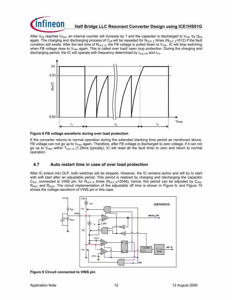
After VFB reaches VFBH, an internal counter will increase by 1 and the capacitor is discharged to VFBL by QFB again. The charging and discharging process of CFB will be repeated for NOLP_E times (NOLP_E=512) if the fault condition still exists. After the last time of NOLP_E, the FB voltage is pulled down to VFBL, IC will stop switching when FB voltage rises to VFBH again. This is called over load/ open loop proteciton. During the charging and discharging period, the IC will operate with frequency determined by Ichg_min and ICS.
Figure 8 FB voltage waveform during over load protection
If the converter returns to normal operation during the extended blanking time period as mentioned above, FB voltage can not go up to VFBH again. Therefore, after FB voltage is discharged to zero voltage, if it can not go up to VFBH within TOLP_R (1.28ms typically), IC will reset all the fault timer to zero and return to normal operation.
4.7 Auto restart time in case of over load protection
After IC enters into OLP, both switches will be stopped. However, the IC remains active and will try to start with soft start after an adjustable period. This period is realized by charging and discharging the capacitor CINS ,connected to VINS pin, for NOLP_R times (NOLP_R=2048), hence, this period can be adjusted by CINS, RINS1 and RINS2. The circuit implementation of the adjustable off time is shown in Figure 9, and Figure 10 shows the voltage waveform of VINS pin in this case.
Figure 9 Circuit connected to VINS pin

Half Bridge LLC Resonant Converter Design using ICE1HS01G
Application Note 12 August 2009 13
Time
VINS_H
t1 t2 t3
VINS_L
Figure 10 VINS voltage waveform during restart time
As shown in Figure 10, the voltage across CINS is discharged to VINS_L (0.5V typically) when IC goes into OLP at time t1. After that, an internal constant current source IINST is turned on to charge CINS. Once the voltage at VINS pin is charged to VINS_H (4.5V typically), the current source will be turned off and CINS is discharged by another switch Q3 to VINS_L again. The charging and discharging of CINS comprise one cycle. This cylce time is also influenced by the bus voltage. The charging and discharging time of CINS can be approximated as
−⋅+⋅
−⋅+⋅⋅⋅−=
INSLeqINSTINS
eqBUS
INSHeqINSTINS
eqBUS
INSeqingch
VRIRR
V
VRIRR
VCRt
1
1arg ln
−⋅
−⋅⋅⋅−=
INSHINS
eqBUS
INSLINS
eqBUS
INSeqingdich
VRR
V
VRR
VCRt
1
2
1
2
2arg ln
where Req is the equivalent resistance for parallelling of RINS1 and RINS2,
21 // INSINSeq RRR =
Req2 is the equivalent resistance for parallelling of RINS1, RINS2 and RQ3 (900ohm typically).
3212 //// QINSINSeq RRRR =
IC will repeat the charging and discharging process for NOLP_R times (NOLP_R=2048). After that, IC will turn off the switches for both charging and discharging. In addition, the current source for hysteresis will be turned on and another blanking time of TBL_VINS, the time between t2 and t3 as shown in Fiugre 10 will be added so that VINS pin fully recovers and represents the bus voltage information. IC will start the soft start after the additional blanking time in case VVINS is higher than the VVINSon.

Half Bridge LLC Resonant Converter Design using ICE1HS01G
Application Note 12 August 2009 14
5 Design Example A 24V 200W LLC demoboard using ICE1HS01G is now available. In order to simplify and speed up this IC’s feature evaluation, no PFC stage is implemented, so 280Vac input is recommended to feed this 200W demboard, thus around 380Vdc across bulk capacitor can be obtained.
5.1 Design Specifications
The LLC stage is usually used to follow a PFC stage, thus the nominal input voltage for LLC stage can be specified as:
Vdc400_ =nominV
Output voltage is specified as 24V: V24=outV
Output current is specified as 8A: A8=outI
The required hold-up time: ms20=hT
The PFC output capacitor: uF220=oC
5.2 Define System Specifications
The estimated efficiency: 93.0=η
The input power will then be: W45.206=⋅
=η
outoutin
IVP
During the hold up time, the input voltage for LLC stage drops gradually to a lower level, and the output voltage of LLC stage is still required to be regulated. The required minimum input DC voltage can be estimated as:
V95.34922_min_ =
⋅⋅−=
o
hinnominin C
TPVV
The resonant frequency is selected as: kHz100=rf
5.3 Define the Required Voltage Gain of the Resonant Network
The integrated magnetic solution is often be used for LLC resonant design. The resonant inductance rL is often combined with the transformer into a single magnetic part. The transfomer’s physical model is shown in Figure 11, where the topological analogy with the inductive part of the LLC resonant tank circuit is apparent.
Figure 11 LLC integrated transformer model
Figure 12 Transformer primary referred model

Half Bridge LLC Resonant Converter Design using ICE1HS01G
Application Note 12 August 2009 15
The transformer’s all primary referred model is shown as Figure 12, where eqn is the equivalent turn ratio. All the elements related to leakage flux are located on the primary side.
If Lp is defined as the primary inductance mearured at primary side with secondary winding open, Lp will be the sum of Lr and Lm. Considering the influence of secondary leakage inductance, the equivalent turn ratio can be estimated as [4]:
1−
=
−
=
mmn
LLLnn
rp
peq
where n is the transformer’s physical turn ratio;
m is the ratio between primary inductance pL and resonant inductance rL : rp LLm =
The equivalent circuit for LLC resonant network is ploted as Figure 13.
Figure 13 Equivalent circuit for LLC resonant network
where rC is the resonant capacitor;
rL is the resonant inductance, which is made by the transformer primary leakage inductance and the reflected secondary leakage inductance;
mL is the magnetizing inductane;
2_effR is the effective load resistance considering the influence of secondary leakage inductance:
out
outeqeff I
VnR ⋅⋅= 222_
8π
The input RMS voltage acinV _ across the resonant network can be calculated as:
dcinacin VV __2π
=
where dcinV _ is the DC input voltage for LLC stage, which is usually powered by frontend PFC stage.
The output RMS voltage acoutV _ across the effective load resistance is:
eqoutacout nVV ⋅=π
22_
Thus the voltage gain can be calculated as:dcin
outeq
acin
acout
VVn
VV
G__
_ 2==
As shown in Figure 13, the resonant network and the load acts as a voltage divider, the expression of the voltage gain can be obtained as:

Half Bridge LLC Resonant Converter Design using ICE1HS01G
Application Note 12 August 2009 16
( )
( )
( )( ) ( ) ( ) 2222222
2
2
2
2
2
2
_ 111
1
111
12
ee
rrp
r
dcin
outeq
QmFFFm
mF
Qmff
ffj
ff
mff
VVn
G−−+−⋅
−=
⋅−⋅
−⋅
+
−
−⋅
==
with the following parameter definitions:
right-side resonant frequency: rr
r CLf
π21
=
left-side resonant frequency: rp
p CLf
π21
=
inductance ratio: r
p
LL
m =
normalized frequency: rffF =
quality factor: out
outeq
r
r
effr
re I
VnCL
RCLQ ⋅⋅⋅=⋅= 2
22_
81π
.
Considering
1−
=
−
=
mmn
LLLnn
rp
peq , another voltage gain G′ directly related to the physical turn ratio
n can be expressed as:
( ) ( ) ( ) ( ) 2222222
2
2
2
2
2
2
_ 111
)1(
111
)1(2
ee
rrp
r
dcin
out
QmFFFm
mmF
Qmff
ffj
ff
mmff
VnVG
−−⋅+−⋅
−⋅=
⋅−⋅
−⋅
+
−
−⋅
==′
For LLC topology, when operating close to the resonant point, the frequency’s load-insensitivity can be achieved, thus the optimal operation point is put close to the resonant frequency point. Hence, the switching frequency is recommended to be put at the resonant point when LLC operates with nominal input voltage:
rnoms ff =_
Based on above G′ expression, the voltage gain at nomsf _ and nominV _ can be given as:
1−=
mmGnom
Hence the gain at nomsf _ is determined by choosing the inductance ratio m .
Too small m means smaller pL and bigger rL , which will result in poor coupling of the transformer and deteriorate the efficiency due to increased circulating current. Typically m is set between 3 to 7.
If the chosen m value is: 5=m

Half Bridge LLC Resonant Converter Design using ICE1HS01G
Application Note 12 August 2009 17
Then the voltage gain at nomsf _ and nominV _ can be calculated as:
12.11=
−=
mmGnom
Accordingly the maximum required voltage gain is at min_inV and can be given as:
28.1min_
_max =⋅= nom
in
nomin GVV
G
5.4 Calculate the Transformer Turns Ratio
Assuming the secondary rectifier diode voltage drop fV is:
V6.0=fV
The transformer turns ratio will be: ( ) 909.92
_ ≈=⋅+⋅
= nomfout
nomin GVV
Vn
5.5 Calculate the Effective Load Resistance
The effective load resistance is: Ω=⋅⋅= 97.1968 22
out
outeff I
VnRπ
If considering the transformer’s secondary leakage inductance, the effective load resistance is:
Ω==⋅⋅= 57.15782
222_
nom
eff
out
outeqeff G
RIVnR
π
5.6 Determine the Resonant Network
The m value is chosen same as mentioned above: 5=m .
The gain equation can be recalculated as:
( ) ( ) ( ) 22
2
22222222
2
18.02015
1
111
)1(2
−⋅⋅+
⋅−
=−−⋅+−⋅
−⋅==′
FFQ
FFQmFFFm
mmFVnVG
eein
out
Then the frequency response of the voltage gain G′ vs F and eQ is plotted as following:

Half Bridge LLC Resonant Converter Design using ICE1HS01G
Application Note 12 August 2009 18
Normalized frequency
0.2 0.4 0.6 0.8 1 1.20.5
0.75
1
1.25
1.5
1.75
2
2.25
2.5
1.4
F
Qe=0.2
Qe=0.3
Qe=0.4
Qe=0.5
Qe=0.6
Qe=0.8
Qe=0.7
Gpk=1.47
Gmax=1.28
Gnom=1.12
Figure 14 Voltage gain vs normalized frequency
As discussed above, the maximum required voltage gain maxG is calculated to meet the hold up time requirement. In addition, in order to ensure stable ZVS operation and meet the output voltage regulation requirement when LLC operates at the lowest allowable input voltage, the peak gain PKG at full load
condition should be somehow higher than maxG .
Considering 15% margin: 47.115.1 max =⋅= GGpk
According to Figure 14, the voltage gain when 5.0=eQ can meet this peak gain requirement.
Accordingly, the resonant capacitor can be selected as:
nF2.202
1
2_
=⋅⋅⋅
=effre
r RfQC
π
Also the resonant inductance will then be: ( )
uH39.1252
12 =⋅⋅
=rr
r CfL
π
The primary inductance is: uH97.626=⋅= rp LmL
When using the integrated magnetic solution, the resonant inductance rL is implemented by the leakage
inductance, hence the value of rL is not easy to control. The resonant network parameters based on above calculation often needs to be changed according to the measured inductance values and the standard capacitance value.

Half Bridge LLC Resonant Converter Design using ICE1HS01G
Application Note 12 August 2009 19
5.7 Transformer Design
The worst case for LLC transformer’s operation is that when LLC operates at minimum switching frequency when input DC voltage drops to the lowest allowable voltage and full load.
The maximum required voltage gain occurs at min_inV and can be given as:
28.1min_
_max =⋅= nom
in
nomin GVV
G
Base on Figure 14, it can be roughly estimated that
28.1=G when 78.0=F and 5.0=eQ
Accordingly the minimum switching frequency can be obtained as:
kHz78min =⋅= rfFf
According to Faraday’s Law, the minimum number of primary turns for LLC transformer can be estimated as:
( ) ( )e
fout
e
fouteqp ABfmm
VVnABfVVn
N⋅∆⋅⋅−
+⋅=
⋅∆⋅
+⋅==
minminmin_ 2)1(2
The transformer core is selected as PC47 EER32, its effective cross sectional area is: 2mm6.79=eA
To avoid saturation, the flux density swing (peak to peak) is chosen as:
T45.0=∆B
The minimum number of primary turns can be calculated as:
( )44.35
mm6.79T45.0kHz78212.1)V6.0V24(9
2)1( 2min
min_ =⋅⋅⋅⋅
+⋅=
⋅∆⋅⋅−
+⋅=
e
foutp ABfmm
VVnN
The actual number of primary turns can be selected as: 36=pN
Accordingly the number of secondary turns is: 4== nNN ps
5.8 Primary current, Resonant Cap Voltage and OCP level
The primary RMS current flowing through resonant capacitor can be obtained as:
( )( ) A3.1
24221
22
_ =
−⋅⋅⋅
++
⋅⋅
⋅=rpr
foutoutrmsr LLMf
VVnn
II πη
Hence, the primary peak current is: A84.12 __ =⋅= rmsrpkr II
The over current protection level is set to about 50% margin of this peak current:
A76.2%)501( _ =⋅+= pkrocp II
The maximum voltage across resonant capacitor occurs at nominal input dc voltage and OCP level:
V36.43622
_max_ =
⋅⋅+=
rr
ocpnominCr Cf
IVV
π

Half Bridge LLC Resonant Converter Design using ICE1HS01G
Application Note 12 August 2009 20
Thus, a 630V film capacitor with low ESR is recommened to be used as resonant capacitor.
5.9 Output Rectifier
For the output winding with center tap, the output diode voltage stress is
( ) V2.492 =⋅+= foutd VVV
The RMS current flowing through the output rectifier diode can be estimated as:
A28.64
=⋅= outd II π
6 Experiment Verification A 200W half bridge LLC resonant converter demoboard with ICE1HS01G is implemented as shown in Figure 15. Also the full load efficiency of LLC stage has reached 94.35% as shown in Figure 22. The detailed schematic circuit is shown in Figure 16 and Figure 17. The specification of this 200W LLC demoboard is listed as following table 1.
Table 1 200W Demoboard Specification Normal Input AC voltage 280Vac
Normal DC bulk voltage 400Vdc
Mains under voltage protection point 300Vdc
Auxiliary power supply for IC VCC 15Vdc
Normal output full load 24V/8A
Switching frequency 100kHz @ 24V/8A and 400Vdc input
6.1 200W 24V HB LLC Resonant Converter using ICE1HS01G
Figure 15 200W half bridge LLC resonant converter demoboard using ICE1HS01G

Half Bridge LLC Resonant Converter Design using ICE1HS01G
Application Note 21 12 August 2009
6.2 Schematic of 200W Half Bridge LLC Resonant Converter
+ C1220u/450V
Q1IPA50R299CP
Q2IPA50R299CP
C222nF/630V
R1424k+1k
D13 VF30100SG
D14 VF30100SG
+C16
1000uF/35V
+C17
1000uF/35V
L2 1.2u/7.5A
+ C19470uF/35V
C7680pF5%
2
1
3
4
IC2SFH615A-2
C9
220pF / 630V
C8 220nF
D91N4148
D101N4148
R16
150
R15
75
24V
GND
R121M
R1322k
R1730k / 1%
R181k1 / 1%
R193k6 / 1%
R23
2k2
R225k6
R211k1
R20 27k
23
1 IC3
TL431
+ C151uF/35V
ZD515V
C10 68nF
C622nF5%
R112M
R102M
VCCHGLGGND
QHGQHSQLGQLS
VCCHGLGGND
QHGQHSQLGQLS
VINS
GNDHG
CS FBFMIN
LGVCC
IC1
ICE1HS01G
FUSE15A/250V
2 3
1 4
L3
3.3m
H/4
.6A
RT1S237/5
CX1
220nF/275Vac
CX2100nF/275Vac
L N1
CY1
2n2/Y1
CY2
2n2/Y1
2
4
3
1
BR1KBU8G (8A / 400V)
3
11
28
1
910
5
6
TR1
ER42/ER35/ER32
R1 N.C.
D11N.C.
D12N.C.
+ C1147uF N.C.
L1 Short
VR1S10k/275
C12100nF
+
C547uF/50V
+ C181000uF/35V
C20 N.C.
R24N.C.R25N.C.R26N.C.
C14 N.C.
C13
N.C.
R27N.C.
R28N.C.
CY3 2n2/Y1
Figure 16 Schematics of 200W half-bridge LLC resonant converter
VCC
HG
LG
GND
QHG
QHS
QLG
QLS
2
1
8
7
6
5
TR2
R2150
R310k
D11N4148
D21N4148 C3
100nF
R4150
R510k
D31N4148
D41N4148 C4
100nF
R610
R710
R810
D51N4148
D61N4148
D71N4148
D81N4148
1
23Q3 BC546
1
23Q6 BC546
23
1Q5
BC557
23
1Q8
BC557
23
1
Q7 BC557
23
1
Q4 BC557
ZD115V
ZD215V
ZD315V
ZD415V
R910
Figure 17 Schematics of driver circuit
The AC line input side comprises the input fuse FUSE1 as overcurrent protection. The X2 Capacitors CX1, CX2 and Choke L3 and Y1 capacitors CY1 and CY2 forms a main filter to minimize the feedback of RFI into the main supply. RT1 is placed in series with input to limit the initial peak inrush current. After the bridge rectifier BR1, together with a smoothing capacitor C1, a voltage of 300VDC to 400 VDC is provided, depending on mains input voltage, to simulate the real operation condition with front end PFC pre_regulator.
As shown in Figure 17, a cost-effective pulse transformer TR2 is used to transmit the driver signal to MOSFETs for isolation purpose. The totem pole driver circuits (optional), including a NPN and a PNP transistor is used to drive the pulse transformer. In the secondary side of the driver circuit, R7, R9, D6, D8, Q5, and Q8 are used to accelerate the turn-off speed of MOSFET. If the sink impedance of the pulse transformer is enough, these circuits can also be saved. In this case, a simplified driver circuit is shown in Figure 18.

Half Bridge LLC Resonant Converter Design using ICE1HS01G
Application Note 22 12 August 2009
HG
LG
QHG
QHS
QLG
QLS
3R3
3R3
1u0
11R
3R3
11R
1N4148
1N4148
15V
15V
15V
15V
3R3
2
1
5
6
7
8
MBR160
MBR160
Figure 18 A simplified driver circuit
6.3 PCB Bottom Layer
Figure 19 Solder side copper – View from component side
6.4 Transformer Construction • Bobbin: Split type EC32, Horizontal version from TDK • Core: PC47 ER32 from TDK • Primary inductance: 616µH±5%, Gapped between Pin 1 and Pin 3 • Leakage inductance: 136µH±5%, measured between Pin 1 and Pin 3 by shorting (Pin 7 & 8) • Measured at frequency of 40kHz

Half Bridge LLC Resonant Converter Design using ICE1HS01G
Application Note 23 12 August 2009
Figure 20 LLC resonant transformer electrical diagram
Figure 21 LLC resonant transformer winding position
Figure 22 LLC resonant transformer complete – top view Table 2 LLC resonant transformer winding characteristics
6.5 Test Results Efficiency Mesurements
Table 3 shows the output voltage measurements at the nominal input bulk voltage 400Vdc, with different load conditions. The bulk voltage 400Vdc is directly supplied from Chroma programmable DC power supply. Hense, there is no current flowing through the bridge rectifier, and the measured efficiency is actually the LLC stage’s efficiency. Table 3 Efficiency measurements @ Vbulk=400Vdc
24Vout [V] 24Vout current [A]
Pinput_main power [W]
Pinput_IC and Driver [W] Poutput [W] Efficiency [%]
23.92 7.980 201.8 15*0.034=0.51 190.882 94.35

Half Bridge LLC Resonant Converter Design using ICE1HS01G
Application Note 24 12 August 2009
23.92 6.977 175.9 15*0.034=0.51 166.890 94.60 23.93 5.989 150.9 15*0.034=0.51 143.317 94.65 23.93 4.986 125.6 15*0.034=0.51 119.315 94.61 23.93 3.984 100.5 15*0.034=0.51 95.337 94.38 23.93 2.996 75.9 15*0.034=0.51 71.694 93.83 23.93 1.993 51.1 15*0.035=0.525 47.692 92.38 23.93 0.990 26.5 15*0.035=0.525 23.691 87.66
Figure 23 LLC stage efficiency The power losses due to IC and driver circuit are both included. In addition, the efficiency values were measured after 30 minutes of warm-up at full load.
Resonant stage operating waveforms
a. full load 8A output b. light load 0.5A output Figure 24 Resonant stage operating waveforms Figure 24 shows the resonant waveforms during steady state operation of this LLC resonant circuit at nominal dc input voltage 400Vdc and full load 8A and light load 0.5A condition. Channel 1 shows the Mosfet drive signal Vgs. The half bridge square voltage, which driving the resonant circuit, is shown in channel 2. It

Half Bridge LLC Resonant Converter Design using ICE1HS01G
Application Note 25 12 August 2009
can be found that the zero voltage switching is achieved. The primary resonant current is shown by channel 4, it is almost sinusoidal because the operating point is close to the resonant frequency rf .
Secondary side operating waveforms
a. full load 8A output b. light load 0.5A output Figure 25 Secondary rectifier diode voltage stress and flowing current Figure 25 shows the voltage across the secondary rectifier diode, the voltage stress equals to 51V. The current flowing through rectifier diode is also shown by channel 4. This current shape is almost a sine wave, and its average value equals to one half the output current.
7 References [1] ICE1HS01G datasheet, Infineon Technologies AG, 2008
[2] RW ERICKSON, D MAKSIMOVIC: ‘Fundamentals of power electronics’ (Kluwer Academic Publishers, 2001), pp. 705–755
[3] B Yang: ‘Topology investigation for front end DC/DC power conversion for distributed power system’, PhD thesis, Virginia Polytechnic Institute and State University, 2003
[4] S.De Simone.: ‘Design-oriented steady state analysis of LLC resonant converters based on FHA’, SPEEDAM 2006, 2006.
[5] Mingping Mao, Dimitar Tchobanov, Dong Li, Martin Maerz, Tobias Gerber, Gerald Deboy, Leo Lorenz.: ‘Analysis and design of a 1MHz LLC Resonant Converter with Coreless transformer driver’. PCIM Conference, Shanghai. 2007
[6] M Mao, D Tchobanov, D Li, M Maerz.: ‘Design optimization of a 1MHz half bridge CLL resonant converter’. IET Power Electronics, 2008, Vol.1, pp. 100-108.