anomalous oscillations with an impatt diode oscillations with an impatt diode p.j.dewaard...
TRANSCRIPT

Philips tech. Rev. 32, 361-369,1971, No. 9/10/11/12 361
Anomalous oscillations with an IMPATT diode
P. J. de Waard
Introduetion
In 1967 it was discovered that an IMPATT-diodeoscillator can have a mode of oscillation entirely differ-ent from the normal transit-time oscillations dealt within the two preceding articles [ll. This "anomalousmode" [2l is remarkable in the first place for itshigh efficiency. Recently anomalous oscillations wereproduced with an efficiency of 75% [3l, whereas notmuch more than 15% can be expected for normaloscillations [4l. Moreover the power,output (more than10W) and current density (a few thousands of Afcm2)
are much higher than are found with normal oscilla-tions.A further characteristic of the anomalous mode is
the frequency, which is lower than that of a transit-timeoscillator and far less affected by the diode used in thecircuit. For example, a diode suitable for transit-timeoscillations of a few GHz can be made to give anom-alous oscillations that can be tuned to any frequencyin the range from about 100MHz to 1 GHz by adjust-ing the circuit.These anomalous oscillations are easy to produce in
circuits that can be tuned to different frequencies at thesame time. Usually, therefore, they are produced andinvestigated in circuits in which the diode is connectedto a coaxial line containing various tuning slugs. Inanomalous oscillation a section of the coaxial linefunctions as a delay line, whose length determines theoscillation frequency. It is generally assumed that nor-mal transit-time oscillations are essential to the excita-tion of the anomalous oscillation. The circuit musttherefore be tuned not only to the required anomalousmode but also to a normal mode which appears in thecircuit as a higher harmonic of the anomalous one.Apart from the transit-time mode and the high-
efficiency anomalous mode, other kinds of oscillationmay occur in IMPATT-diode oscillators, for examplerelaxation oscillations. Because of their low efficiencyand low frequency, however, they are of little interestand ~re regarded more as unwanted side-effects. Al-though they all really come under the term "anomalousoscillations", this term will be confined to the high-efficiency mode in this article.
Oscillations can only occur when there is an elementin the circuit that has a negative resistance at theIr. P. J. de Waard is with Philips Research Laboratories, Eind-hoven.
oscillation frequency. The d.c. or low-frequencycurrent-voltage characteristic of an IMPATT diodealone shows a positive differential resistance at all cur-rent values. At Philips Research Laboratories we havefound however that ifthe d.c. or low-frequency charac-teristic is measured while the diode is actually oscilla-ting in the anomalous mode in a circuit of the typeindicated above, then quite a different shape is ob-tained. This curve includes a large section with nega-tive slope. A characteristic measured in this way is de-scribed as "quasi-static". The diodes investigated wereall "punch-through" diodes, i.e. diodes whose middlesection is so lightly doped that at breakdown the deple-tion layer extends to both contact regions, and the fieldgradient in the middle section is small (see fig. 2a). Ithas been possible to generate anomalous oscillationsonly with diodes of this type in our experimental ar-rangement tsi,As a working hypothesis it was assumed that the
measured quasi-static characteristic forms the basis forthe anomalous oscillations, in other words that it canbe identified with a "true" characteristic valid for in-stantaneous values of current and voltage. Startingfrom this working hypothesis it was possible to makecomputer simulations of the oscillations; these simula-tions consisted of calculations of the current and volt-age variations for an equivalent circuit in which thediode was simply defined by its measured characteristic.This gives useful information about the operation ofthe oscillator as a whole, and in particular made it pos-sible to optimize the circuit by comparison ofthe com-puted results for various values of the circuit param-eters. Computer simulations of this type are widelyused in microwave work, owing to the difficulty ofvarying the parameters in the actual circuit.In these investigations of the anomalous oscillator as
a whole no account has been taken of what happens inthe diode itself. Nevertheless, in the next section we[1) D. de Nobel and M. T. Vlaardingerbroek, IMPATT diodes;
this issue, page 328.K. Mouthaan, IMPATT-diode oscillators; this issue, page345.
[2) H. J. Prager, K. K. N. Chang and S. Weisbrod, Proc. IEEE55, 586, 1967.
[3) D. F. Kostishack, Proc. IEEE 58, 1282, 1970.[4) See the tables on page 336 and page 350 of the two preced-
ing articles in this issue [1).
[5) Anomalous oscillations have been obtained elsewhere withdiodes of a different type.

362 P. J. DE WAARD Philips tech. Rev. 32, No. 9/10/11/12
\
shall consider some ideas concerning the processes inthe diode, and a qualitative explanation for the shapeof the measured characteristic will be given, since theseideas strongly support the working hypothesis. How-ever, the picture of the effects in the diode given thereis no more than speculative, and differs to some extentfrom computer simulations of these effects that havebeen made elsewhere on the basis of the equationsdescribing the fundamental processes in the diode [6].
The other sections will present in turn a discussionof the equivalent circuit used for the computer simula-tions and its use in understanding the operation of theanomalous oscillator, the efficiency predicted by thetheory, the experimental arrangement and some resultsof the measurements and calculations.
The quasi-static diode characteristic
An example of a quasi-static characteristic, measuredon one of our diodes, is given by the solid curve infig. 1.It has already been mentioned that curves of this typeare obtained while the circuit is oscillating. More accur-ately, the circuit is first adjusted to oscillate in theanomalous mode, and from then on, without makingany other adjustment, the average current 10 throughthe diode (the supply current) is changed and theaverage voltage Vo across the diode is measured as afunction of 10; this gives the solid curve. If, however,oscillation is prevented by damping the circuit in someway, the dashed curve is obtained. Of course, for agiven 10 that is not too small, there are various settingsat which anomalous oscillations occur. There is notmuch difference, however, in the characteristics meas-ured. Where differences of any significanee occur, thecharacteristic with the deepest minimum is taken asrepresentative of the diode, for reasons that will laterbecome clear.
By combining some ideas [7] [8] about high-currenteffects in the diode, a qualitative explanation of thisbehaviour can be given. Let us divide the charac-teristic into two parts. The first part can be explainedas an ordinary rectifying effect [9], as follows. Supposethat 10 is slowly increased from zero. At first thevoltage rises rapidly until it reaches the breakdownvalue Vb. When 10 exceeds the starting current, transit-time oscillations begin, so that in addition to the d.c.voltage there is an a.c. voltage across the diode, whoseamplitude increases with the supply current. Ifthe peakvoltage in each period were to become much greaterthan Vb, a very large current pulse would be expectedin each period, owing to the exponential nature of theavalanche effect.The limited average current, however,rules this out. The average voltage therefore adjustsitself differently, so that the peak value is not so far
150V
lil
t 100
....---- 1----- -----.....-~Vt,
<, I
~ e-, ->~ ...................50
2 t.; 3 4A, -Ia
Fig. 1. The quasi-static characteristic (solid curve) of a planarsilicon diode, i.e. the d.c. voltage Vo across the diode as a func-tion of the d.c. current 10 through the diode, measured while thediode is in a circuit adjusted to give anomalous oscillation (unless10 is too Iow). If oscillation is prevented, the dashed curve ismeasured. Vb breakdown voltage. Vm and Im are referred to asvalley voltage and valley current.
above Vb. The average voltage thus falls, and this ex-plains the initial part ofthe faIling section ofthe charac-teristic.This explanation does not apply to the whole of the
falling section, because beyond a certain value of thesupply current the amplitude of the transit-time oscilla-tion rises no further [lOl. The following explanation ofthe second section seems to be the most likely one.
Fig. 2a shows a schematic breakdown field profiletypical of the diodes used in these experiments. As dis-cussed in the previous articles, when the current israised slightly an avalanche region is formed near theposition of maximum field-strength, and to the rightof it, in fig. 2a, a drift region for electrons. On increas-ing the current further two effects arise that can resultin a profile of the type shown in fig. 2b [7]. Sincefigs. 2a and b show the magnitude of the field directedtowards the left a positive charge will result in a nega-tive slope (decreasing from left to right) and a negativecharge will give a positive slope. Consequently, theeffect of the increasing number of electrons is in thefirst place to make the field profile in the drift regionmore and more horizontal, causing the avalanche regionto spread out. Secondly, in the avalanche region thereare large numbers of holes on the left and large num-bers of electrons on the right; the slope is thus negativeon the left and positive on the right, resulting finallyin a dip or "valley" in the field profile. In fig. 2b av-alanching takes place on both sides of the depletionlayer. With a field profile of this type it is reasonableto assume that the characteristic will have a negativeslope, for as the current increases, the sides ofthe valleybecome steeper. Since the depletion layer cannot be-come much wider (if the P+ and the N+ regions are

Philips tech. Rev. 32, No. 9/IOjil/12 ANOMALOUS OSC[LLATJONS 363
doped heavily enough) and the peaks cannot rise farabove the breakdown field, the valley must becomedeeper. The area underneath the curve therefore de-creases, i.e. the voltage drops.
Results of this kind for diodes of this type are obtained quan-titatively if the equations for the field and the hole and electroncurrent are solved numerically [71, starting from analytical ex-pressions for the doping profile and also known expressions [Ill
for the ionization coefficients and drift velocities of electrons andholes in silicon, as functions of the field. Calculations of this typehave been performed at Philips Research Laboratories for oneof the experimental diodes. Results are presented in jig. 3. Thevalley obtained in the field profile when the current reaches acertain value can be seen in fig. 3a. ln fig. 3b it can be seen thatwhen the current is high the hole and electron currents haveabout the same magnitude over a wide region in the middle ofthe diode. In this region there is an almost neutral cloud ofcharge carriers. This is the plasma implicit in the acronymTRA PA TT (trapped plasma avalanche triggered transit), thename often used for diodes oscillating in the anomalous mode.This name, which will not be discussed further here, is based ona somewhat different, more dynamic picture of the processes inthe diode, deduced from the computer simulations of these effectsmentioned earlier ter. In this picture a wave passes through thefield profile during each period. In the picture ouclined herethe field profile simply varies up and down between differentcurves like those illustrated in fig. 3a.
The non-appearance of the negative slope when thediode is not oscillating (fig. 1, dashed curve) can beexplained as follows. If a random fluctuation arises in
O~~~------L_------~--_X
Fig. 2. The field profile assumed in a diode at breakdown (a)and at high current (b). In the diodes used here the depletionlayer extends to the N+ region at breakdown. At low current,avalanching releases holes and electrons in the high-field region(on the left in a); the electrons move through the N region tothe right. At high current, the charge of the holes and electronsgives rise to a profile with a dip or "valley"; A, p, 11 and Dindicate whether the prevailing charge is due to acceptors, holes,electrons or donors, respectively. Avalanching now occurs atboth peaks.
400·r---~-----.------~----~-----'--'kVlcm
a
E
1200~#-~~~~--~
100~--f-----+----+-----+----ll---1
\I'-_
\ bo20 21 22 2] 24jJm
_X
Fig. 3. a) Results of computer calculations of the field E as afunction of x, the distance from the original silicon surface, forvarious values of current density Jo. b) The same for Jvl J«, thefraction of the current carried by holes, for the case whereJo = 2 x 10⁹ A/m2. The calculations were based on the knownvariation [llJ of the ionization coefficients and the drift veloc-ities of holes and electrons in silicon as a function of the field,and on the measured doping profile.
the current distribution in a plane at right angles to thedirection of the current, causing a local increase in cur-rent density, the voltage drop across the depletion layerwill be lower at this position, because of the fallingcharacteristic. Conseq uently more charge carriers aredrawn from the supply regions, and the current densityrises still further. Fluctuations of this kind thus rein-force themselves, and current channels are formed [81.
At the sarne time, however, the current in the supplyregion is also compressed into narrow channels, whoseeffective resistance is thus increased. It is assumed thatthis resistance effect exceeds the negative resistanceeffect in the depletion layer, so that the characteristicof the whole diode nevertheless has a positive slope.The final link in the explanation is the assumption
that it takes so much time for these current channels to
[61 B. C. DeLoach, Jr., and D. L. Scharfetter, JEEE Trans.EO-17, 9, 1970.
17] See H. C. Bowers, I EEE Trans. EO-IS, 343, 1968.[8J A. M. Barnett, IBM J. Res. Devel. 13, 522, 1969.[91 This rectifying effect is discussed in another way in the article
by K. Mouthaan [11; see fig. 13 (page 353).uo: See the article by O. de Nobel and M. T. Vlaardingerbroek [11,
page 338.[11] C. A. Lee, R. A. Logan, R. L. Batdorf, J. J. Kleimack and
W. Wiegmann, Phys. Rev. 134, A 761, 1964.

364 P. J. DE WAARD Philips tech. Rev. 32, No. 9/10/11/12
VD iL. DL
;,! LNCL
lol D
N r-r:
form that the oscillating diode has a falling character-istic: the current then varies so rapidly that the currentchannels have no chance to develop. The tendency forchannels to form increases, however, as the averagecurrent increases, so that above a certain current valuethe voltage increase associated with channel formationbecomes dominant after all. This provides an explana-tion for the rising part of the characteristic (fig. I).
In many respects the IMPATT diode is the dual ofthe Gunn diode [121. The current channels, for instance,correspond to the high-field regions in the Gunn effect.Also, the characteristic of the anomalously oscillatingdiode, if current and voltage are interchanged, is muchlike that of the Gunn diode oscillating in the LSAmode [121.
the diode, which is therefore "half on": vn =tVb;h = 10; i2 = O. Owing to the interaction of theinductance LN with the diode, however, this state iseasily perturbed. Assume, for instance, that a fluctua-tion occurs in the current distribution at the junctionpoint above D, causing h to drop and thus Vn torise accordingly; the 'diode "shuts off" a little. Sincei: + i2 is constant, i2 must rise at the same time. Thisrise induces an emf in LN that opposes iz in thecircuit external to LN. Since VN remains constant atfirst, because the impedance of LN for rapid varia-tions is much greater than that of CN and DL, thereis consequently a further rise of vn. The diodeis thus still further shut off by LN. This processcontinues until the diode is completely shut off. It
Fig. 4. The equivalent circuit for the anomalous oscillator used as the basis for the computersimulations. The diode is defined here as an element with the characteristic of fig. 5. Thecurrent 10 supplied by the current source is divided between the diode D and the rest of thecircuit; 10 = h + is. The network N, in particular the inductance LN, causes the diode toswitch easily from the "switched on" state (h = Im) to the "shut-off" state (h = 0), andvice versa. When the diode shuts off, a voltage and a current front appear at the input ofthedelay line DL (characteristic impedance Zo and delay time r). Part of this signal is reflectedby the low-pass filter F and causes the diode, which had meanwhile switched on again, toshut off once more after a time 2r. Similarly the switching on of the diode causes it toswitch on again after a period 2t: Only the fundamental frequency of the oscillations ispassed by F and arrives via the large bypass capacitor CL in the load RL. The diode and thedelay line should preferably be matched. The coupling network N has an important correctivefunction if there is a mismatch.
Equivalent circuit; operation of the oscillator
The equivalent circuit on which the computer simu-lations were based is shown infig. 4. It is assumed thatthe diode has the characteristic shown infig. 5, whichis a schematic piecewise-linear version of the charac-teristic in fig. 1. In fig. 4 a reverse-biased diode D isconnected to a current source, and there is a delayline DL connected in parallel with D via a couplingnetwork N. The delay line is connected to a matchedload RL through a low-pass filter F. A large bypasscapacitance CL ensures that no d.c. current can flowthrough RL.
This diagram will now be used to explain the opera-tion of the oscillator, assuming for convenience thatthe current h at which vn is equal to Vb (see fig. 5)can be neglected. It is also assumed that the valleyvoltage Vm is zero, and that 10, the value of the sourcecurrent, is half that of the valley current Im.In the steady state the delay line draws no current.
The whole of the supply current 10 then flows through
follows analogously that a fluctuation of the appro-priate sign can easily cause the diode to switch fromthe shut-off to the switched-on state, and vice versa.Once the diode is shut off, iz remains temporarily
constant, the induced emf thus disappears, and VN fol-lows vn. At the same time charge begins to flow intothe delay line. The voltage and current front which thusform at the line input propagate along the line and
-i,Fig. 5. The diode characteristic used in the computer simulations.

Philips tech. Rev. 32, No. 9/10/11/12 ANOMALOUS OSCILLATIONS 365
reach the output after a time r, the delay time. If vand i are the voltage and current at an arbitrary pointof the line, and v - tVb and i are therefore their re-spective deviations from the average steady state, thenthe ratio (v - tVb)/i is equal to Zo, the characteristicimpedance of the line, at any rate as long as there areno reflected signals.It will now be shown that oscillations in which the
diode switches from the switched-on to the shut-off-state and back to the switched-on state again, are self-sustaining. For the time being we shall not be con-cerned with how the oscillation starts, in other words
time ts. + •. The slow component of the voltage andcurrent variation passes the low-pass filter F andvanishes in the matched load. For the fast components,however, F constitutes a short-circuit; these compo-nents are therefore reflected, resulting in a negativevoltage and positive current pulse travelling to the left.The situations just before and just after this reflection- and hence before and after the second reversal,which took place at approximately the same time -can be seen in fig. 6 (t = /2 _:_ ,1 and t = /2 + ,1).The reflected signal reaches the input at the timet = II + 2.. The current pulse arriving there is a
t~ 1 l 1 1 1t, t2 ~+2T' t2+2T' t,+4T' t2+4T'
t
(C: I f;P-=t
t,+l1
Cf) -x -10 __..x
0
I ~ t ti t2-..1
tr 1 tf l t2+..1
~ b A' L A t,+2T'-..1
tt J ~j t, +2T'+..1
Fig. 6. The diode voltage VD as a function of time (above) and voltage and current fronts inthe delay line, each shown a time Ll after a diode reversal and a time zl before the next reversal.The current distribution at the junction point above the diode is shown in the circular insets.
how the first two reversals take place; we shall returnto this point later. We assume that /2 - 1I is smallerthan 2., where II and tz are the times at which thediode first shuts off and then switches on again (fig. 6above). For simplicity let us make /2 roughly equal toII + x, though this is not essential to the argument.Voltage and current distributions in the delay line fol-lowing these reversals are given in fig. 6. Shortly afterthe first reversal (t = II + ,1) there is a front at thebeginning of the line. This reaches the output at- the
"fluctuation" whose sign is such as to shut off thediode again, which had been on since the secondreversal. This is because the current pulse arriving atthe input is a momentary increase of i2 which must beassociated with a decrease of ti, i.e. a variation in the'direction of the shut-off state of the diode. Analogouslythe signal appearing at the output as a result of reflec-tion at time /2 + • causes the diode to switch on again(12) See the article by G. A. Acket, R. Tijburg and P. J. de:
Waard in this issue, page 370.

366 P. J. DE WAARD Philips tech. Rev. 32, No. 9/10/11/12
at time tz + 21".Each event is repeated after a period 21",which is the period of the oscillations.
The question that remains to be answered is how thefirst two reversals come about. For the first reversalthis presents no problem: as we have seen, any arbitraryfluctuation on the initial steady state can cause thediode to switch on or off. The second reversal, after atime of approximately 1",can be attributed to the opera-tion of the coupling network. This forms an LC circuitwhich, excited by the first reversal, reacts like a resona-tor. Here it will be sufficient to note that, if suitablevalues are chosen for the parameters, the computersimulation also shows that oscillations are initiated bya single excitation of the oscillator.
To summarize, the coupling network, driven by thediode plus current source and working into the load Zo,has an inherent tendency to oscillate. The frequency ofthe oscillations, however, is determined by the delayline through the mechanism described above of re-flected signals that initiate diode reversals.
In the ideal case the diode and the delay line arematched (Zo = (Vb - Vm)/Im). In the absence of thecoupling network, the diode reversals can then in prin-ciple take place in any arbitrary way, including instan-taneously. This is w because at each change in VD
(identical with VN if there is no LN) changes can befound in hand iz that correspond to the diode charac-teristic and to the line impedance as well as to the con-ditions that h + iz must be constant. In this caseoscillations can be imagined in which the variation ofvoltage and current is that of a square wave, the voltagevarying between Vm and Vb, the current between L«and approximately zero. If moreover "on" and "off"periods are equally long, then these are the oscillationswith the maximum efficiency. In the event of a mis-match - which cannot always be avoided in practice- currents can arise in the diode that may be largerthan Im. The characteristic then appears to be flatter.The average voltage is greater and the oscillations areno longer "square-wave", two causes of a drop inefficiency.
The coupling network N has an important correctivefunction if there is a mismatch. If Zo is greater than(Vb - Vm)/Im, the delay line responds to a voltagevariation Vb - Vm with a current variation smallerthan Im. This means that with no coupling networkpresent the diode would not switch over completely;the capacitor CN, however, now supplies the missingcurrent variation. Conversely, LN supplies the missingvoltage variation if Zo is too small. Because of theseeffects the waveform of the oscillations is however nolonger purely rectangular.
As noted in the introduction, the practical circuitmust also resonate in a normal transit-time mode, since
the initial part of the characteristic in fig. 1 has a nega-tive slope only because of oscillations in this mode, andanomalous oscillations can only be initiated becauseof this initial part. This feature of the circuit does notappear from the diagram in fig.4, but is implicit in thediode characteristic.
Efficiency
The efficiency of the diode is greatest when it is pro-ducing square-wave oscillations between the peak(10= 0, Vo = Vb) and valley (10 = Im, Vo = Vm) ofthe characteristic, and when the durations of thesestates are equally long. The a.c. current and voltageare in antiphase. The output power of the diode is thenthe product of the square-wave current amplitude ·t/mand the square-wave voltage amplitude -}(Vb - Vm),
i.e. ·Fm(Vb - Vm). The d.c. current required is tIm,at a d.c. voltage of t(Vm + Vb), so that the d.c, powersupplied is tIm(Vm + Vb). Under these conditionsthe efficiency is therefore (Vb - Vm)/(Vb + Vm).
Now only the power WL delivered to the matchedload RL in fig. 4 is useful power; this is the power inthe fundamental component. If la and Va are the cur-rent and voltage amplitudes of this fundamental com-ponent the useful power is tlaVa. From Fourier anal-ysis we know that the amplitude of the fundamentalcomponent of a square wave is 4/n times the square-wave amplitude. The efficiency is thus t X (4/n)2 or0.81 times the value calculated above. The charac-teristic in fig. I, with Vb = 105 V and Vm = 42 V,gives an efficiency of 35 % calculated in this way.The theoretical maximum is reached at Vm = 0and amounts to 81%. As noted in the introduction,oscillations have recently been obtained with anefficiency of 75% [31. If Vm is to have a low value,the two peaks in the field which occur when the cur-rent in the depletion layer is high (see fig. 2b) must benarrow, which implies a steep doping profile.
The experimental arrangement; results
The experimental oscillator is shown in fig. 7. Thelargest item is the coaxial line, which has a charac-teristic impedance of 50 D.. The oscillation frequency isdetermined by the distance between the diode D and thefilter F; the frequency can be adjusted by moving thefilter. For a frequency of 1 GHz - requiring a delaytime 1" of 0.5 ns - the diode/filter spacing must be15 cm (the dielectric is air). The diode is connected tothe power source S through the inner conductor; thesource can supply either d.c. current, or pulses, toprevent thermal overloading of the diode. Since theresistance Rs in the supply line is high (500 Q), the

Philips tech. Rev. 32, No. 9/10/11/12 ANOMALOUS OSCiLLATIONS 367
source is a good approximation to a constant-currentsource. The inductance L« prevents high-frequencyenergy from reaching the supply line. The load RL isa 50 n microwave matched load and is made of atten-uating material. The bypass capacitance CL is a gapin the inner conductor. The low-pass filter F consistsof two metal slugs, which do not make contact withthe inner conductor. Each of these slugs behaves likea capacitor, and the part between them as an induc-tance. The coupling network N consists of two PTFEslugs, which are also used to resonate the circuit in thetransit-time mode.
if the oscillations all occurred on the negative slope ofthe linear part of the true characteristic. In reality,however, both current and voltage go beyond the valleyduring the oscillations, and this means that the averagevalues give an unfavourable picture of the real situa-tion. In the case ofthe Gunn effect, known a.c. voltagesare applied (to avoid the analogue of "current channelformation") and the true characteristic can be calculat-ed from the measured one [12]. In our arrangement,however, the diode is left to oscillate freely; the wave-form and amplitude of the oscillations are unknown,and there is consequently some uncertainty about the
Ls
Fig. 7. The experimental arrangement (schematic). The diode D is mounted at the end of acoaxial line, the length between the diode and the filter F acting as a delay line. The couplingnetwork N and the filter F of fig. 4 are formed by inserting slugs in the line: PTFE slugsfor the coupling network and capacitive metal slugs for the filter. The diode is connected tothe power source S through the inner conductor. Because of the high resistance Rs (500 0)the supply is a good approximation to a constant-current source. Ls inductance, acting ashigh-frequency separation between coaxial line and supply. CL. gap in the inner conductor,acting as a d.c. isolating capacitance. RT" load resistance. G bolometer for power measure-ment. The quasi-static characteristic is deter mined by measuring 10 at A (using a currenttransformer if the supply current is pulsed) and V" at B. The high-frequency diode current i :
is deter mined by measuring the voltage across the disc resistor Rel (I 0), using a samplingoscilloscope at H.
Various types of diode made at Philips ResearchLaboratories were used for exciting oscillations in thisarrangement. The quasi-static 10- Vo characteristic ofeach diode was plotted (10 was measured at A andVo at B), and attempts were made to set the slugs, inparticular N, to the position that gave the lowest pos-sible value of Vm, the valley voltage. According to thetheory, this should yield the highest efficiency. Atypical characteristic of this type was shown in fig. I.The power generated in the anomalous mode was meas-ured with a bolometer in place of the load (at G infig. 7). Some results relating to power and efficiency aregiven in Table I.
The measured efficiency of a planar diode is some-times greater than would be expected from the charac-teristic. The explanation for this is probably as follows.According to our working hypothesis, the quasi-staticcharacteristic measured during oscillations correspondsto the "true" characteristic valid for instantaneousvalues of currents and voltages. This would be correct
Table I. Power and efficiency of the anomalous oscillations ob-tained with various diodes in the arrangement shown in fig. 7.
Diode Supply Frequency Power Efficiency
Si, planar pulsed 0.8-1.5 GHz 30-50 W 40-50%Ge, mesa d.c. I GHz 1.5 W 32%Ge, mesa d.c. 2 GHz 2W 22%
relation between the measured and the true charac-teristic.
[n addition to transit-time oscillations and anomalousoscillations of the type described, unwanted relaxationoscillations can occur in our oscillators. Their frequencyis in general much lower than 1/2r, and they are mainlydetermined by CL, RL, the supply voltage and the diodecharacteristic; the coaxial line has scarcely any effectsince it is only a small fraction ofthe wavelength. Theseoscillations can cause the diode to burn out if CL dis-charges for too long a time, which can happen if CLis large.
368 P. J. DE WAARD Philips tech. Rev. 32, No. 9/10/11/12
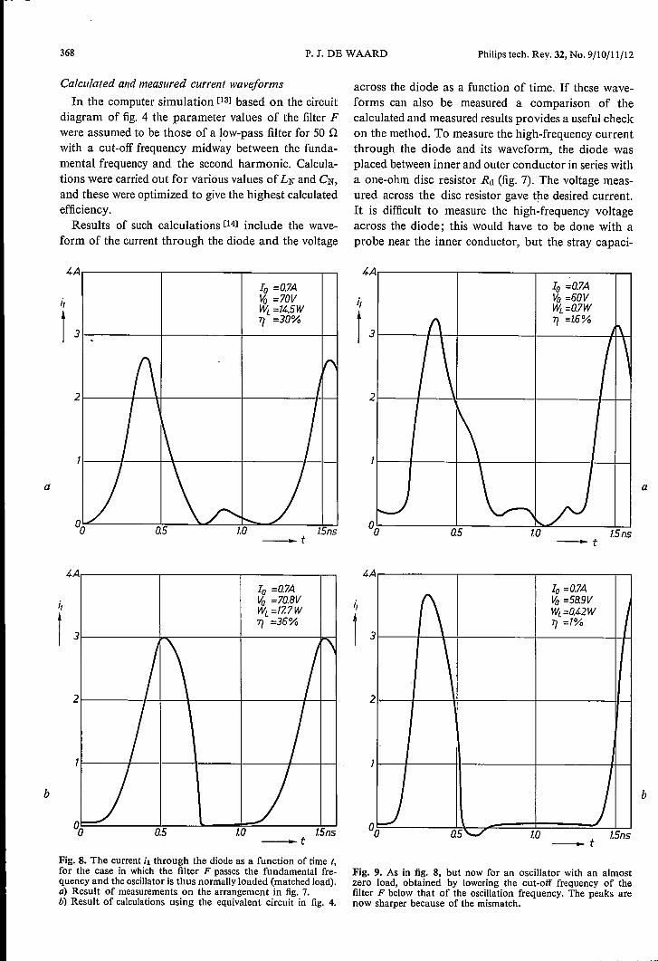
Calculated and measured current waveformsIn the computer simulation [13] based on the circuit
diagram of fig. 4 the parameter values of the filter Fwere assumed to be those of a low-pass filter for 50 Qwith a cut-off frequency midway between the funda-mental frequency and the second harmonic. Calcula-tions were carried out for various values of LN and CN,and these were optimized to give the highest calculatedefficiency.Results of such calculations [14] include the wave-
form of the current through the diode and the voltage
across the diode as a function of time. If these wave-forms can also be measured a comparison of thecalculated and measured results provides a useful checkon the method. To measure the high-frequency currentthrough the diode and its waveform, the diode wasplaced between inner and outer conductor in series witha one-ohm disc resistor Rd (fig. 7). The voltage meas-ured across the disc resistor gave the desired current.It is difficult to measure the high-frequency voltageacross the diode; this would have to be done with aprobe near the inner conductor, but the stray capaci-
4.A 4.A
Ia =0.7A Ia =0.7A
i, L1J =70V i, Va =60V
tWL=14..5W
tWt.=Q7W
1] =30% 1] =1.6%3 3
-t
4.A 4AIa =0.7A
i, L1J =70.8V i,WL =17.7W
1.,., =36%
t 3
a
b
1.0-t
Fig. 8. The current it through the diode as a function of time t,for the case in which the filter F passes the fundamental fre-quency and the oscillator is thus normally loaded (matched load).a) Result of measurements on the arrangement in fig. 7.b) Result of calculations using the equivalent circuit in fig. 4.
a
-t
o
(\Ia =0.7AL1J =5a9VWL=Q42W I1] =1%
\
LJ0 5"-./
b
2
Q 1.0 1.5ns-t
Fig. 9. As in fig. 8, but now for an oscillator with an almostzero load, obtained by lowering the cut-off frequency of thefilter F below that of the oscillation frequency. The peaks arenow sharper because of the mismatch.

Philips tech. Rev. 32, No. 9/10/11/12 ANOMALOUS OSCILLATIONS 369
tance introduced would then make it difficult to tunethe diode to the transit-time frequency. The high-fre-quency measurement was performed with a samplingoscilloscope.To conclude, two examples ofthe results of our meas-
urements and calculations will now be given. Fig. 8shows the r.f. current is. as a function of time for a casewhere the slugs in F were positioned to pass the fun-damental frequency but reflect all higher harmonics.The diode current h is by no means a square wave;this is because, for practical reasons, the coaxial lineand the diode were not matched (Zo = 50 n,(Vb - Vm)flm R! 20 n). Fig.9 gives the results for anoscillator with an almost zero load; this was realizedby setting the slugs in F (and by selecting the param-eters of F in the calculations) in such a way that thefundamental frequency was also almost entirely reflect-ed. This gave a severe mismatch of the coaxialline andits load, and consequently the current peaks throughthe diode were larger and sharper, as can be seen in thefigure. In such a case, of course, the power WL de-livered to the load and the efficiency1] are very small.
[13] These were carried out on the Philips Electrologica ELX-8computer at Philips Research Laboratories.
[14] P. J. de Waard, Proc. 1971 European Microwave Conf.,Stockholm, Vol. 1, paper A 9/1.
Since the measurements and calculations were almostindependent of one another, the agreement between thetwo is highly satisfactory in a qualitative sense (thesharpness of the peaks) as well as in the quantitativesense (the magnitude of the current). Since the modelis really a rather crude one, in particular because of itsidentification of the quasi-static with the true charac-teristic, it is not surprising that there are still distinctdiscrepancies.
Summary. In 1967 it was found that an IMPATT-diode oscillatorcould operate in a mode that differed from the normal transit-time mode. This "anomalous mode" is characterized by a muchlower frequency and a much higher efficiency. The quasi-staticcharacteristic of the IMPATT diodes used here (the relation be-tween d.c. voltage and current while the diode is oscillating) hasa region with negative slope, and the anomalous oscillations areattributed to this. At low currents the negative slope is explainedas a rectifying effect associated with transit-time oscillations. Athigher currents it is explained by the occurrence of a valley in theinternal field profile, as a result of the charge of the holes andelectrons produced. As the current rises, this valley becomesdeeper and the voltage decreases. Because of the formation of"current channels" no negative slope is measured in the staticstate; during oscillation, however, the current channels have notime to develop. Owing to the negative slope the diode is unstableand easily switches from the shut-off to the switched-on state.In an anomalous oscillator each reversal is initiated by signalsreflected from the end of a delay line to which the diode is con-nected. In the oscillator used here the delay line is a coaxial linewith several slugs for tuning and matching. A computer simula-tion of the oscillations has been made, based on an equivalentcircuit in which the diode is defined by the measured quasi-staticcharacteristic. The current and voltage waveforms calculatedfrom this model give a satisfactory agreement with the resultsof the measurements.